CN101276721A - Plasma display panel and manufacturing method thereof - Google Patents
Plasma display panel and manufacturing method thereofDownload PDFInfo
- Publication number
- CN101276721A CN101276721ACNA2008100845197ACN200810084519ACN101276721ACN 101276721 ACN101276721 ACN 101276721ACN A2008100845197 ACNA2008100845197 ACN A2008100845197ACN 200810084519 ACN200810084519 ACN 200810084519ACN 101276721 ACN101276721 ACN 101276721A
- Authority
- CN
- China
- Prior art keywords
- discharge
- display panel
- plasma display
- discharge electrodes
- electrode
- Prior art date
- Legal status (The legal status is an assumption and is not a legal conclusion. Google has not performed a legal analysis and makes no representation as to the accuracy of the status listed.)
- Pending
Links
- 238000004519manufacturing processMethods0.000titleclaimsabstractdescription19
- 239000000758substrateSubstances0.000claimsabstractdescription70
- 229910052751metalInorganic materials0.000claimsabstractdescription30
- 239000002184metalSubstances0.000claimsabstractdescription30
- 239000000463materialSubstances0.000claimsabstractdescription15
- 125000006850spacer groupChemical group0.000claimsabstractdescription3
- 238000002955isolationMethods0.000claimsdescription46
- 238000000034methodMethods0.000claimsdescription30
- 229920002120photoresistant polymerPolymers0.000claimsdescription29
- 229910052782aluminiumInorganic materials0.000claimsdescription23
- XAGFODPZIPBFFR-UHFFFAOYSA-NaluminiumChemical compound[Al]XAGFODPZIPBFFR-UHFFFAOYSA-N0.000claimsdescription23
- 230000003647oxidationEffects0.000claimsdescription23
- 238000007254oxidation reactionMethods0.000claimsdescription23
- 230000008569processEffects0.000claimsdescription19
- 238000005530etchingMethods0.000claimsdescription9
- 239000002904solventSubstances0.000claimsdescription6
- 230000007935neutral effectEffects0.000claimsdescription4
- 239000004254Ammonium phosphateSubstances0.000claimsdescription3
- 229910000148ammonium phosphateInorganic materials0.000claimsdescription3
- 235000019289ammonium phosphatesNutrition0.000claimsdescription3
- NGPGDYLVALNKEG-UHFFFAOYSA-Nazanium;azane;2,3,4-trihydroxy-4-oxobutanoateChemical compound[NH4+].[NH4+].[O-]C(=O)C(O)C(O)C([O-])=ONGPGDYLVALNKEG-UHFFFAOYSA-N0.000claimsdescription3
- MNNHAPBLZZVQHP-UHFFFAOYSA-Ndiammonium hydrogen phosphateChemical compound[NH4+].[NH4+].OP([O-])([O-])=OMNNHAPBLZZVQHP-UHFFFAOYSA-N0.000claimsdescription3
- WYXIGTJNYDDFFH-UHFFFAOYSA-Qtriazanium;borateChemical compound[NH4+].[NH4+].[NH4+].[O-]B([O-])[O-]WYXIGTJNYDDFFH-UHFFFAOYSA-Q0.000claimsdescription3
- 229910044991metal oxideInorganic materials0.000claims2
- 150000004706metal oxidesChemical class0.000claims2
- TWNQGVIAIRXVLR-UHFFFAOYSA-Noxo(oxoalumanyloxy)alumaneChemical compoundO=[Al]O[Al]=OTWNQGVIAIRXVLR-UHFFFAOYSA-N0.000claims1
- 238000002360preparation methodMethods0.000claims1
- 239000010408filmSubstances0.000description58
- 239000010410layerSubstances0.000description51
- 230000004888barrier functionEffects0.000description15
- 238000002048anodisation reactionMethods0.000description10
- 239000007789gasSubstances0.000description10
- OAICVXFJPJFONN-UHFFFAOYSA-NPhosphorusChemical compound[P]OAICVXFJPJFONN-UHFFFAOYSA-N0.000description9
- 238000007743anodisingMethods0.000description9
- 239000011521glassSubstances0.000description6
- 230000001590oxidative effectEffects0.000description6
- 238000012545processingMethods0.000description6
- 230000005684electric fieldEffects0.000description5
- 239000002994raw materialSubstances0.000description5
- QVGXLLKOCUKJST-UHFFFAOYSA-Natomic oxygenChemical compound[O]QVGXLLKOCUKJST-UHFFFAOYSA-N0.000description4
- 229910052760oxygenInorganic materials0.000description4
- 239000001301oxygenSubstances0.000description4
- 238000005498polishingMethods0.000description4
- 239000000126substanceSubstances0.000description4
- 229910018072Al 2 O 3Inorganic materials0.000description3
- MUBZPKHOEPUJKR-UHFFFAOYSA-NOxalic acidChemical compoundOC(=O)C(O)=OMUBZPKHOEPUJKR-UHFFFAOYSA-N0.000description3
- 239000000853adhesiveSubstances0.000description3
- 230000001070adhesive effectEffects0.000description3
- 239000002245particleSubstances0.000description3
- 238000002834transmittanceMethods0.000description3
- QAOWNCQODCNURD-UHFFFAOYSA-NSulfuric acidChemical compoundOS(O)(=O)=OQAOWNCQODCNURD-UHFFFAOYSA-N0.000description2
- 238000005452bendingMethods0.000description2
- 230000008901benefitEffects0.000description2
- 239000003086colorantSubstances0.000description2
- 230000008878couplingEffects0.000description2
- 238000010168coupling processMethods0.000description2
- 238000005859coupling reactionMethods0.000description2
- 238000005520cutting processMethods0.000description2
- 238000010586diagramMethods0.000description2
- 238000000227grindingMethods0.000description2
- 230000005283ground stateEffects0.000description2
- 230000001771impaired effectEffects0.000description2
- 230000005596ionic collisionsEffects0.000description2
- 150000002500ionsChemical class0.000description2
- 238000012986modificationMethods0.000description2
- 230000004048modificationEffects0.000description2
- 238000004080punchingMethods0.000description2
- 238000000926separation methodMethods0.000description2
- OKTJSMMVPCPJKN-UHFFFAOYSA-NCarbonChemical compound[C]OKTJSMMVPCPJKN-UHFFFAOYSA-N0.000description1
- 240000006829Ficus sundaicaSpecies0.000description1
- 238000010521absorption reactionMethods0.000description1
- 239000012790adhesive layerSubstances0.000description1
- PNEYBMLMFCGWSK-UHFFFAOYSA-Naluminium oxideInorganic materials[O-2].[O-2].[O-2].[Al+3].[Al+3]PNEYBMLMFCGWSK-UHFFFAOYSA-N0.000description1
- 230000015572biosynthetic processEffects0.000description1
- 229910052799carbonInorganic materials0.000description1
- 239000003054catalystSubstances0.000description1
- 229910010293ceramic materialInorganic materials0.000description1
- 244000145845chatteringSpecies0.000description1
- 229910052593corundumInorganic materials0.000description1
- 230000006866deteriorationEffects0.000description1
- 238000011161developmentMethods0.000description1
- 239000003989dielectric materialSubstances0.000description1
- 238000003487electrochemical reactionMethods0.000description1
- 239000003792electrolyteSubstances0.000description1
- 238000000635electron micrographMethods0.000description1
- 230000005281excited stateEffects0.000description1
- 230000002349favourable effectEffects0.000description1
- 230000006872improvementEffects0.000description1
- 239000012535impuritySubstances0.000description1
- 238000009413insulationMethods0.000description1
- 229910052745leadInorganic materials0.000description1
- 239000011159matrix materialSubstances0.000description1
- 239000007769metal materialSubstances0.000description1
- 229910052759nickelInorganic materials0.000description1
- 235000006408oxalic acidNutrition0.000description1
- 230000001681protective effectEffects0.000description1
- 230000009467reductionEffects0.000description1
- 238000011160researchMethods0.000description1
- 239000011347resinSubstances0.000description1
- 229920005989resinPolymers0.000description1
- 239000003566sealing materialSubstances0.000description1
- 239000010409thin filmSubstances0.000description1
- 230000003313weakening effectEffects0.000description1
- 238000003466weldingMethods0.000description1
- 229910001845yogo sapphireInorganic materials0.000description1
Images


Classifications
- H—ELECTRICITY
- H01—ELECTRIC ELEMENTS
- H01J—ELECTRIC DISCHARGE TUBES OR DISCHARGE LAMPS
- H01J11/00—Gas-filled discharge tubes with alternating current induction of the discharge, e.g. alternating current plasma display panels [AC-PDP]; Gas-filled discharge tubes without any main electrode inside the vessel; Gas-filled discharge tubes with at least one main electrode outside the vessel
- H01J11/20—Constructional details
- H01J11/22—Electrodes, e.g. special shape, material or configuration
- H—ELECTRICITY
- H01—ELECTRIC ELEMENTS
- H01J—ELECTRIC DISCHARGE TUBES OR DISCHARGE LAMPS
- H01J9/00—Apparatus or processes specially adapted for the manufacture, installation, removal, maintenance of electric discharge tubes, discharge lamps, or parts thereof; Recovery of material from discharge tubes or lamps
- H01J9/24—Manufacture or joining of vessels, leading-in conductors or bases
- H01J9/241—Manufacture or joining of vessels, leading-in conductors or bases the vessel being for a flat panel display
- H01J9/242—Spacers between faceplate and backplate
- H—ELECTRICITY
- H01—ELECTRIC ELEMENTS
- H01J—ELECTRIC DISCHARGE TUBES OR DISCHARGE LAMPS
- H01J11/00—Gas-filled discharge tubes with alternating current induction of the discharge, e.g. alternating current plasma display panels [AC-PDP]; Gas-filled discharge tubes without any main electrode inside the vessel; Gas-filled discharge tubes with at least one main electrode outside the vessel
- H01J11/10—AC-PDPs with at least one main electrode being out of contact with the plasma
- H01J11/16—AC-PDPs with at least one main electrode being out of contact with the plasma with main electrodes provided inside or on the side face of the spacers
- H—ELECTRICITY
- H01—ELECTRIC ELEMENTS
- H01J—ELECTRIC DISCHARGE TUBES OR DISCHARGE LAMPS
- H01J11/00—Gas-filled discharge tubes with alternating current induction of the discharge, e.g. alternating current plasma display panels [AC-PDP]; Gas-filled discharge tubes without any main electrode inside the vessel; Gas-filled discharge tubes with at least one main electrode outside the vessel
- H01J11/20—Constructional details
- H01J11/22—Electrodes, e.g. special shape, material or configuration
- H01J11/24—Sustain electrodes or scan electrodes
- H—ELECTRICITY
- H01—ELECTRIC ELEMENTS
- H01J—ELECTRIC DISCHARGE TUBES OR DISCHARGE LAMPS
- H01J11/00—Gas-filled discharge tubes with alternating current induction of the discharge, e.g. alternating current plasma display panels [AC-PDP]; Gas-filled discharge tubes without any main electrode inside the vessel; Gas-filled discharge tubes with at least one main electrode outside the vessel
- H01J11/20—Constructional details
- H01J11/22—Electrodes, e.g. special shape, material or configuration
- H01J11/32—Disposition of the electrodes
- H—ELECTRICITY
- H01—ELECTRIC ELEMENTS
- H01J—ELECTRIC DISCHARGE TUBES OR DISCHARGE LAMPS
- H01J11/00—Gas-filled discharge tubes with alternating current induction of the discharge, e.g. alternating current plasma display panels [AC-PDP]; Gas-filled discharge tubes without any main electrode inside the vessel; Gas-filled discharge tubes with at least one main electrode outside the vessel
- H01J11/20—Constructional details
- H01J11/34—Vessels, containers or parts thereof, e.g. substrates
- H01J11/36—Spacers, barriers, ribs, partitions or the like
- H—ELECTRICITY
- H01—ELECTRIC ELEMENTS
- H01J—ELECTRIC DISCHARGE TUBES OR DISCHARGE LAMPS
- H01J9/00—Apparatus or processes specially adapted for the manufacture, installation, removal, maintenance of electric discharge tubes, discharge lamps, or parts thereof; Recovery of material from discharge tubes or lamps
- H01J9/02—Manufacture of electrodes or electrode systems
- H01J9/18—Assembling together the component parts of electrode systems
- H01J9/185—Assembling together the component parts of electrode systems of flat panel display devices, e.g. by using spacers
- H—ELECTRICITY
- H01—ELECTRIC ELEMENTS
- H01J—ELECTRIC DISCHARGE TUBES OR DISCHARGE LAMPS
- H01J2211/00—Plasma display panels with alternate current induction of the discharge, e.g. AC-PDPs
- H01J2211/20—Constructional details
- H01J2211/22—Electrodes
- H01J2211/24—Sustain electrodes or scan electrodes
- H01J2211/245—Shape, e.g. cross section or pattern
- H—ELECTRICITY
- H01—ELECTRIC ELEMENTS
- H01J—ELECTRIC DISCHARGE TUBES OR DISCHARGE LAMPS
- H01J2211/00—Plasma display panels with alternate current induction of the discharge, e.g. AC-PDPs
- H01J2211/20—Constructional details
- H01J2211/22—Electrodes
- H01J2211/32—Disposition of the electrodes
- H01J2211/326—Disposition of electrodes with respect to cell parameters, e.g. electrodes within the ribs
- H—ELECTRICITY
- H01—ELECTRIC ELEMENTS
- H01J—ELECTRIC DISCHARGE TUBES OR DISCHARGE LAMPS
- H01J2211/00—Plasma display panels with alternate current induction of the discharge, e.g. AC-PDPs
- H01J2211/20—Constructional details
- H01J2211/34—Vessels, containers or parts thereof, e.g. substrates
- H01J2211/36—Spacers, barriers, ribs, partitions or the like
- H01J2211/361—Spacers, barriers, ribs, partitions or the like characterized by the shape
- H01J2211/363—Cross section of the spacers
Landscapes
- Engineering & Computer Science (AREA)
- Physics & Mathematics (AREA)
- Plasma & Fusion (AREA)
- Manufacturing & Machinery (AREA)
- Chemical & Material Sciences (AREA)
- Materials Engineering (AREA)
- Gas-Filled Discharge Tubes (AREA)
Abstract
Translated fromChinese
Description
Translated fromChinese相关申请的交叉引用Cross References to Related Applications
本申请要求2007年3月21日提交于韩国知识产权局的韩国专利申请No.10-2007-0027819的权益,该申请的全部内容通过引用被并入本文。This application claims the benefit of Korean Patent Application No. 10-2007-0027819 filed with the Korean Intellectual Property Office on March 21, 2007, the entire contents of which are hereby incorporated by reference.
技术领域technical field
本发明涉及利用气体放电显示图像的等离子体显示面板和制造等离子体显示面板的方法,更具体地,涉及一种具有高发光效率和改进结构并适于批量生产的等离子体显示面板和制造这种等离子体显示面板的方法。The present invention relates to a plasma display panel for displaying images using gas discharge and a method for manufacturing the plasma display panel, and more particularly, to a plasma display panel having high luminous efficiency and an improved structure suitable for mass production and manufacturing the same A method for a plasma display panel.
背景技术Background technique
采用等离子体显示面板的平板显示设备具有优良的特性,例如,其具有高图像质量,超薄,重量轻,具有可以宽视角观看的大屏幕,还可利用简单的制造方法容易地制造成大尺寸。因此,平板显示设备被视为下一代大平板显示设备。Flat panel display devices using plasma display panels have excellent characteristics such as high image quality, ultra-thin, light weight, large screens that can be viewed from a wide viewing angle, and can be easily manufactured in large sizes using simple manufacturing methods . Therefore, the flat panel display device is regarded as a next-generation large flat panel display device.
等离子体显示面板根据其驱动方法可分为直流(DC)型、交流(AC)型、和混合型。另外,等离子体显示面板根据放电结构可分为对向放电型和表面放电型。最近,主要使用三电极表面放电的等离子体显示面板。The plasma display panel can be classified into a direct current (DC) type, an alternating current (AC) type, and a hybrid type according to its driving method. In addition, plasma display panels can be classified into a facing discharge type and a surface discharge type according to a discharge structure. Recently, three-electrode surface discharge plasma display panels are mainly used.
为了解决三电极表面放电结构的问题,例如,荧光物材料的恶化,可见光透过率的下降,和发光效率的下降,对具有新结构的等离子体显示面板的研究正在积极进行。In order to solve the problems of the three-electrode surface discharge structure, such as deterioration of phosphor materials, decrease in visible light transmittance, and decrease in luminous efficiency, research on plasma display panels with new structures is actively being conducted.
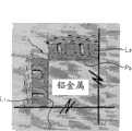
图1是在韩国专利公开No.2005-0104003中公布的等离子体显示面板的分解立体图。等离子体显示面板包括相互面对并在其间具有预定的距离的前基板10和后基板20,和沿相互垂直的方向设置用于限定基板10与20之间放电空间(S)的前阻隔肋31和后阻隔肋24。在前阻隔肋31中,第一放电电极35和第二放电电极45被埋置并且相互分离,从而在放电空间(S)中形成显示放电。前阻隔肋31完全覆盖放电电极34和45,以防止电极由于离子碰撞而损坏,并提供对放电有利的环境,并且,前阻隔肋31由电介质材料形成。荧光物材料25应用在由后阻隔肋限定的区域中。另外,沿着与放电电极35和45交叉的方向延伸的寻址电极22设置在后基板20上,其中埋置有寻址电极22的电介质层21设置在后基板20与后阻隔肋24之间。FIG. 1 is an exploded perspective view of a plasma display panel disclosed in Korean Patent Laid-Open No. 2005-0104003. The plasma display panel includes a front substrate 10 and a
在图1的等离子体显示面板中,放电通过限定放电空间(S)的侧壁产生,因此,应用在后基板20上的荧光物材料25不会由于离子碰撞而劣化。另外,在前基板10侧上的不透明电极被去除,因而改善可见光的向上透过率。此外,放电可通过放电空间(S)的所有侧壁产生,等离子体可集中在放电空间(S)的中心部分上,因此,可显著增加紫外线的产生。In the plasma display panel of FIG. 1, the discharge is generated through the sidewalls defining the discharge space (S), and thus, the phosphor material 25 applied on the
然而,由于等离子体显示面板的结构,其中放电电极35和45埋在阻隔肋31中,因此,使用传统制造方法批量生产等离子体显示面板存在局限性,并且,等离子体显示面板由于制造过程中的问题而不能商业化。However, due to the structure of the plasma display panel in which the discharge electrodes 35 and 45 are buried in the barrier ribs 31, there is a limitation in mass-producing the plasma display panel using the conventional manufacturing method, and the plasma display panel is problem and cannot be commercialized.
发明内容Contents of the invention
本发明提供具有新结构并允许高发光效率且适于批量生产的等离子体显示面板及其制造方法。The present invention provides a plasma display panel having a new structure and allowing high luminous efficiency and suitable for mass production and a method of manufacturing the same.
本发明还提供具有改进放电稳定性和改进耐久性的等离子体显示面板及其制造方法。The present invention also provides a plasma display panel having improved discharge stability and improved durability and a method of manufacturing the same.
根据本发明的一方面,提供一种等离子体显示面板,包括:相互分离的前基板和后基板;在所述前基板与所述后基板之间相互面对的两个或更多个电极板,所述两个或更多个电极板通过包括在每个板中的相应开口图样一起形成放电空间,其中,所述两个或更多个电极板中的每一个包括:多个放电电极,其延伸并围绕所述放电空间的至少一部分,并在接触所述放电空间或邻近所述放电空间的拐角处具有圆形弯曲部分;和隔离元件,其在所述放电电极之间整体形成,用于支撑所述放电电极和使所述放电电极相互隔离,并由用于形成所述放电电极的金属的氧化物材料形成。According to an aspect of the present invention, there is provided a plasma display panel comprising: a front substrate and a rear substrate separated from each other; two or more electrode plates facing each other between the front substrate and the rear substrate , the two or more electrode plates together form a discharge space through a corresponding opening pattern included in each plate, wherein each of the two or more electrode plates includes: a plurality of discharge electrodes, extending and surrounding at least a part of the discharge space, and having a rounded bent portion at a corner contacting the discharge space or adjacent to the discharge space; and a spacer member integrally formed between the discharge electrodes, with for supporting the discharge electrodes and isolating the discharge electrodes from each other, and is formed of an oxide material of the metal used to form the discharge electrodes.
根据本发明的另一方面,提供一种等离子体显示面板,包括:相互分离的前基板和后基板;和在所述前基板与所述后基板之间相互面对的第一电极板和第二电极板,所述第一电极板和第二电极板通过包括在每个板中的对应的开口图样一起形成放电空间;其中,所述第一和第二电极板中的每一个包括:多个放电电极,其延伸并围绕所述放电空间的至少一部分,并在接触所述放电空间或邻近所述放电空间的拐角处具有圆形弯曲部分;和隔离层,其与所述放电电极形成竖直台阶,支撑所述放电电极和使所述放电电极相互隔离,并由用于形成所述放电电极的金属的氧化物材料形成。According to another aspect of the present invention, there is provided a plasma display panel, comprising: a front substrate and a rear substrate separated from each other; and a first electrode plate and a second electrode plate facing each other between the front substrate and the rear substrate. Two electrode plates, the first electrode plate and the second electrode plate together form a discharge space through a corresponding opening pattern included in each plate; wherein each of the first and second electrode plates includes: a plurality of a discharge electrode extending and surrounding at least a part of the discharge space, and having a rounded curved portion at a corner contacting the discharge space or adjacent to the discharge space; and an isolation layer vertically formed with the discharge electrode The straight steps support and isolate the discharge electrodes from each other and are formed of an oxide material of the metal used to form the discharge electrodes.
根据本发明的另一方面,提供一种等离子体显示面板,包括:相互分离的前基板和后基板;和在所述前基板和所述后基板之间相互面对的第一电极板和第二电极板,所述第一电极板和所述第二电极板通过包括在每个板中的相应开口图样一起形成放电空间,其中,所述第一和第二电极板中的每一个包括:放电电极,其包括放电部分和将所述放电部分相互电连接的导电部分,其中每个放电部分包括围绕所述放电空间的放电表面和在接触所述放电表面的拐角上的圆形弯曲部分;和至少一个桥,其整体形成在相邻放电电极之间,以支撑所述放电电极并使所述放电电极相互隔离。According to another aspect of the present invention, there is provided a plasma display panel, comprising: a front substrate and a rear substrate separated from each other; and a first electrode plate and a second electrode plate facing each other between the front substrate and the rear substrate. Two electrode plates, the first electrode plate and the second electrode plate together form a discharge space through a corresponding opening pattern included in each plate, wherein each of the first and second electrode plates includes: a discharge electrode comprising a discharge portion and a conductive portion electrically connecting the discharge portions to each other, wherein each discharge portion includes a discharge surface surrounding the discharge space and a circular bent portion at a corner contacting the discharge surface; and at least one bridge integrally formed between adjacent discharge electrodes to support the discharge electrodes and isolate the discharge electrodes from each other.
根据本发明的另一方面,提供一种制造等离子体显示面板的方法,所述等离子体显示面板包括阵列设置的多个放电空间,延伸并围绕所述放电空间的多个放电电极,和连接所述放电电极并互相电绝缘的隔离层,所述方法包括:制备原材料金属板;形成第一光刻胶(PR)掩模,其覆盖所述放电电极形成在所述金属板的一表面上的部分;形成第二PR掩模,其覆盖所述放电电极形成在所述金属板的另一表面上的部分;选择性地蚀刻所述金属板的被所述第一PR掩模暴露的表面;选择性地蚀刻所述金属板的被所述第二PR掩模暴露的另一表面;去除所述第一PR掩模和所述第二PR掩模;在中性电解溶剂中进行阳极化处理,用于氧化所述金属板以在所述放电电极的表面上形成氧化物膜,并且用于隔离在所述放电电极之间的部分以形成隔离元件;重复所述处理以制造至少两个金属板;堆叠所述金属板以相互面对,并且,将所述金属板设置为相互垂直;并且,将前基板和后基板相互联结,同时利用熔接密封材料插入所述堆叠的金属板。According to another aspect of the present invention, there is provided a method of manufacturing a plasma display panel including a plurality of discharge spaces arranged in an array, a plurality of discharge electrodes extending and surrounding the discharge spaces, and connecting the discharge spaces. The discharge electrodes and the isolation layer electrically insulated from each other, the method includes: preparing a raw material metal plate; forming a first photoresist (PR) mask, which covers the discharge electrode formed on one surface of the metal plate forming a second PR mask covering a portion where the discharge electrode is formed on the other surface of the metal plate; selectively etching a surface of the metal plate exposed by the first PR mask; selectively etching the other surface of the metal plate exposed by the second PR mask; removing the first PR mask and the second PR mask; anodizing in a neutral electrolytic solvent , for oxidizing the metal plate to form an oxide film on the surface of the discharge electrode, and for isolating a portion between the discharge electrodes to form an isolation element; repeating the process to produce at least two metal stacking the metal plates to face each other, and arranging the metal plates to be perpendicular to each other; and coupling the front substrate and the rear substrate to each other while inserting the stacked metal plates with a welding sealing material.
附图说明Description of drawings
本发明的上述和其他特征及有利之处,通过参照附图详细描述其示例性实施例将变得更显而易见,其中:The above and other features and advantages of the present invention will become more apparent from the detailed description of exemplary embodiments thereof with reference to the accompanying drawings, in which:
图1是在韩国专利No.2005-0104003中公开的等离子体显示面板的分解立体图;1 is an exploded perspective view of a plasma display panel disclosed in Korean Patent No. 2005-0104003;
图2是根据本发明实施例的等离子体显示面板的分解立体图;2 is an exploded perspective view of a plasma display panel according to an embodiment of the present invention;
图3是图2中的等离子体显示面板沿线III-III和III′-III′的横截面图;3 is a cross-sectional view of the plasma display panel in FIG. 2 along lines III-III and III'-III';
图4是显示图2中的等离子体显示面板中的电极布置的立体图;4 is a perspective view showing an arrangement of electrodes in the plasma display panel in FIG. 2;
图5和6分别是显示通过对铝产品进行氧化处理而获得的具有尖拐角和圆拐角的氧化物膜的横截面图;5 and 6 are cross-sectional views showing oxide films having sharp corners and rounded corners, respectively, obtained by oxidation treatment of an aluminum product;
图7是在通过施加预定电压而损坏的孔周围的氧化物膜的照片;7 is a photograph of an oxide film around a hole damaged by applying a predetermined voltage;
图8是根据本发明另一实施例的等离子体显示面板的分解立体图;8 is an exploded perspective view of a plasma display panel according to another embodiment of the present invention;
图9是图8中的等离子体显示面板沿线VII-VII和VII′-VII′的横截面图;9 is a cross-sectional view of the plasma display panel in FIG. 8 along lines VII-VII and VII'-VII';
图10是图8中所示电极板的放大立体图;Figure 10 is an enlarged perspective view of the electrode plate shown in Figure 8;
图11A至11I是图示根据本发明另一实施例的制造等离子体显示面板的方法的横截面图;11A to 11I are cross-sectional views illustrating a method of manufacturing a plasma display panel according to another embodiment of the present invention;
图12是图示本发明的阳极化处理的处理示意图;Figure 12 is a process schematic diagram illustrating the anodizing process of the present invention;
图13是显示氧化物膜结构的剖切立体图;13 is a cutaway perspective view showing the structure of an oxide film;
图14是显示了根据本发明实施例制造的氧化物膜结构的照片。FIG. 14 is a photograph showing the structure of an oxide film manufactured according to an embodiment of the present invention.
具体实施方式Detailed ways
根据本发明实施例的等离子体显示面板将参照附图进行详细的描述。A plasma display panel according to an embodiment of the present invention will be described in detail with reference to the accompanying drawings.
第一实施例first embodiment
图2是根据本发明的实施例的等离子体显示面板的分解立体图,图3是图2中的等离子体显示面板沿线III-III和III′-III′的横截面图。为了说明方便,图3的横截面显示了沿图2的线III′-III′的第二电极板140。另外,图4是在图2中所示放电电极135和145的放大立体图。2 is an exploded perspective view of a plasma display panel according to an embodiment of the present invention, and FIG. 3 is a cross-sectional view of the plasma display panel in FIG. 2 along lines III-III and III'-III'. For convenience of illustration, the cross-section of FIG. 3 shows the
等离子体显示面板包括相互面对的前基板110和后基板120,和在前基板110与后基板120之间相互面对而形成多个放电空间S的第一电极板130和第二电极板140。前基板110变为显示图像的表面,因此,前基板110可以是具有优良透光率的玻璃基板。The plasma display panel includes a
第一电极板130和第二电极板140为通过下述方式形成的集成板,即,通过在原材料金属板上形成预定的电极图样,然后氧化金属板以隔离金属板的一部分。在下文中,第一和第二电极板130和140的结构将进行更详细的描述。沿纵向和水平方向设置的多个开口形成在第一和第二电极板130和140中的每一个中,多个放电空间S通过形成在相应位置的开口的组合形成。在此,放电空间S为这样的空间,其中,形成用于产生显示放电的预定电场并填充以通过放电被激发的放电气体。在本实施例中,由于第一和第二电极板130和140被设置为相互面对并一起形成放电空间S,因而由第一和第二电极板130和140形成的上、下部变为放电空间S的一部分。在本申请文件中,为了说明方便,由板130或140形成的部分可被称为放电空间S,然而,由板130和140形成的部分实际上仅形成放电空间S的一部分。The
由于圆形开口图样形成在第一和第二电极板130和140中,因此,每个放电空间S形成为柱状。然而,当多边形开口图样形成在第一和第二电极板130和140中时,每个放电空间S可形成为包括六面体形状在内的各种多面体形状。另外,放电空间S的形状不限于此,只要放电气体可填充在放电空间S中即可。Since a circular opening pattern is formed in the first and
沿一方向(X方向)延伸同时围绕放电空间S的多个第一放电电极135形成在第一电极板130中。第一放电电极135可由具有高电导率的金属材料形成,从而使由于其自身阻抗所致的热损失最小化,例如,第一放电电极135可由铝材料形成。每个第一放电电极135包括:围绕放电空间S并参与放电操作的放电部分135a,和将放电部分135a相互电连接并向放电部分135a提供驱动功率的导电部分135b。放电部分135a限定对应于放电部分135a的形状的放电空间S,因此,放电部分135a的形状可根据实施例改变,以形成不同类型的放电空间。圆形弯曲部分R1沿放电空间135a的限定放电空间的内表面形成。圆形弯曲部分R1沿放电部分135a的上、下拐角形成为环。圆形弯曲部分R1将随后进行更详细的描述。A plurality of
同时,放电部分135a在附图中被形成为完全围绕放电空间S,然而,放电部分135a可仅围绕放电空间S的一部分,只要其形成的电场足够大以在放电空间中产生放电即可。这可有助于限制放电电流。在这里,放电空间135a的一部分可开口,开口部分可以是相对于放电空间135a形成竖直台阶的隔离层131。Meanwhile, the
另一方面,氧化物膜135t利用例如阳极化的氧化处理形成在第一放电电极135的外表面上而至预定厚度(To)。第一放电电极135的被氧化物膜135t覆盖的内部未被氧化,并保留为保持导电性的核心部135c。第一放电电极135可使用氧化物膜135t被电绝缘。例如,氧化物膜135t可由通过使铝(AL)氧化而形成的Al2O3形成。在接触放电空间S的表面上所形成的氧化物膜135t防止放电电极135和145相互直接电连接,并防止放电电极135由于带电粒子的碰撞而损坏,即,实现传统电介质层的功能。On the other hand, the
考虑到耐受电压特性,保护放电电极135的氧化物膜135t可以形成为具有足够的厚度,氧化物膜135的厚度(To)可通过控制处理条件(例如,氧化处理中的施加电流,电解质的选择,和处理时间)而最优化。由于第一放电电极135的表面被氧化物膜135t覆盖,因此,可防止第一和第二放电电极135和145之间的电短路。The
相对于氧化物膜135t的形成,圆形弯曲部R1沿放电部分135a的接触放电空间S的边缘形成。通常,由于放电空间S通过冲压电极板130形成,因而接触放电空间S的表面是冲压处理中的切制表面,而尖边缘可能会形成在切制表面的拐角上。另一方面,由于氧化物材料从例如阳极化处理的氧化处理中的产品的外露表面长大,因此,难以在通过切制处理形成的尖边缘上形成具有致密结构的氧化物材料。因此,在当前实施例中形成圆形弯曲部分R1以去除尖边缘,从而防止氧化物膜135t的生长基底由于所述边缘而变弱,并在包括拐角的整个表面连续形成氧化物膜135t。With respect to the formation of the
同时,与第一放电电极135整体形成的隔离层131形成在第一放电电极135之间。第一放电电极135通过隔离层131在结构上相互支持,因此,可防止第一电极板130的颤动或第一电极板130的弯曲,并且易于在制造过程中搬运第一电极板130。如图所示,隔离层131形成第一电极板130的整个区域,但第一放电电极135的部分除外。开口可形成在隔离层131的一部分上,以促进由于阳极化处理特性的氧化处理,也就是说,氧化通过表面发生。在这里,氧化可通过开口的侧表面进行。Meanwhile, the
隔离层131在结构上支撑第一放电电极135并在第一放电电极135之间隔离。例如,当对应于隔离层131的部分通过将其上形成有电极图样的铝板氧化被隔离时,隔离层131可由Al的氧化材料Al2O3形成。The
隔离层131相对于第一放电电极135形成竖直台阶,并形成至相对较薄的厚度(Ti)。例如,隔离层131在其上、下部上相对于第一放电电极135形成台阶d1和d2,并且,隔离层131的厚度Ti较小。隔离层131的厚度Ti可通过阳极化处理中的处理条件确定。在通过阳极化处理而自表面向内的氧化处理过程中,隔离层131的厚度可能足够低以完全氧化对应于隔离层131的部分。如果隔离层131形成为厚于厚度Ti,则隔离层131的连接第一放电电极135的内部未氧化,并保持导电性。因此,第一放电电极135通过隔离层131电短路,隔离层131包括处理余量在内的厚度必须形成得足够薄。为了形成具有相互不同厚度的第一放电电极135和隔离层131的结构,隔离层131的部分从作为原材料的铝板的两侧蚀刻,以与第一放电电极135形成台阶结构。在这里,如果在隔离层131与第一放电电极135之间的台阶d1和d2被设定为彼此相同,则从两侧进行的蚀刻处理可对称进行,因此,可改善操作的方便。The
另一方面,只要隔离层131形成得较薄而使得隔离层131的内部可通过氧化处理完全氧化,则台阶的d1和d2可形成在第一放电电极135的两表面上,否则,可相对于第一放电电极135的一表面形成深台阶,并且可在第一放电电极135的另一表面的相同高度处形成平坦表面。On the other hand, as long as the
另一方面,在第一放电电极135与隔离层131之间的竖直台阶d1和d2被设定为具有相互不同的深度,使得第一放电电极135保持导电性,并且,隔离层131可在相同的氧化条件下完全隔离。然而,形成在隔离层131的上、下部上的台阶空间(g)可设置为,当在放电空间S中的混杂气体被排放和放电气体填充在放电空间S中时的气体排放路径和引入路径。因此,可减少用于排放-填充处理的时间,并且,可保持放电气体的不纯度较高而在放电空间S中没有任何混杂气体,从而改善放电操作的稳定性。On the other hand, the vertical steps d1 and d2 between the
面对第一电极板130的第二电极板140设置在第一电极板130下。第二电极板140可具有类似于第一电极板130的结构。更具体地,多个放电空间S设置在第二电极板140上,并且,沿y方向延伸并围绕放电空间S的多个第二放电电极145形成在第二电极板140中。每个第二放电电极145包括:围绕放电空间S并参与放电操作的放电部分145a,和将放电部分145a相互电连接并向放电部分145a提供驱动功率的导电部分145b。圆形弯曲部R2沿放电部分145a的接触放电空间S的边缘形成。The
第二放电电极145可沿y方向延伸,与沿x方向延伸的第一放电电极135交叉,因此,一个放电电极可作为寻址电极,另一放电电极可作为扫描电极,从而通过无源矩阵(PM)驱动方法允许选择其中将发生显示放电的放电空间S。例如,第一放电电极135可作为扫描电极,第二放电电极145可作为寻址电极。然而,本发明的技术范围不限于上述电极结构,并且,本发明可应用于下述结构,其中,第一和第二放电电极相互平行设置,且形成沿与放电电极交叉的方向延伸的另外的寻址电极(未示出)。在这里,第一和第二放电电极之一可作为扫描电极以产生寻址放电,用于和寻址电极一起选择放电空间。The
第二放电电极145通过在第二放电电极145之间的隔离层141填充区域被支撑并相互隔离。另外,隔离层141形成较小的厚度(Ti),同时与第二放电电极145一起形成台阶d1和d2。更具体地,隔离层141可与第二放电电极145的上、下表面形成具有较低厚度Ti的台阶d1和d2。另一方面,尽管第一和第二电极板130和140在图中未显示,但其可利用例如在其间不导电的电介质粘合层相互联结。The
面对前基板110的后基板120可为玻璃形成的玻璃基板。槽120′形成在后基板120的内表面上以对应于放电空间S,荧光物125沿槽120′应用。槽120′限定荧光物125的应用区域,并增大荧光物125的应用区域。为了实现全色显示,荧光物125应用为不同的颜色。例如,在彩色图像利用三基色显示的情况下,红、绿和蓝的荧光物125在槽120′中交替地应用。另外,根据所应用的荧光物125的种类,例如红、绿或蓝光的单色光从每个放电空间S发出,因此,彩色图像利用单色光显示。The
在下文中,将描述等离子体显示面板的操作。当交流(AC)电压应用于第一和第二放电电极135和145时,预定电场形成在放电空间S中以形成放电,因此,从寻址放电获得的壁电荷和由放电气体的电离形成的带电粒子沿放电电极135与145之间的放电路径移动,以产生显示放电。显示放电通过放电电极135和145的限定放电空间S的侧表面沿竖直方向形成为闭合环。因此,放电电极135和145的侧表面变为放电表面。填充在放电空间S中的放电气体通过与沿放电路径移动的带电粒子的碰撞被激发,并然后稳定至基态,从而产生对应于激发态与基态之间的能量差的紫外线。紫外线125通过荧光物125转变为可见光,然后,可见光朝前基板110投射,从而显示被用户识别的预定图像。Hereinafter, the operation of the plasma display panel will be described. When an alternating current (AC) voltage is applied to the first and
在下文中,将描述形成在放电电极135和145中的弯曲部分R1和R2的操作。如上所述,圆形弯曲部分R1和R2形成在第一和第二电极135和145的接触放电空间S的拐角上。邻近弯曲部分R1和R2的放电表面对应于切制表面,此切制表面当原材料板被穿孔以形成用于形成放电空间的开口时形成。因此,尖边缘通常沿邻近放电表面的拐角形成。在本实施例中,磨光操作沿放电表面的拐角进行以去除尖边缘,因此,磨光操作之后形成了弯曲部分R1和R2。在这里,磨光操作可以是用于精切削操作的抛光操作,例如,利用化学机械抛光(CMP)设备的抛光垫的化学机械抛光,或利用砂纸的手工操作,从而去除尖边缘。Hereinafter, operations of the bent portions R1 and R2 formed in the
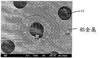
图5是显示通过对具有尖边缘的铝产品进行氧化处理获得的氧化物膜的横截面图,而图6是显示通过对在其拐角部分上具有弯曲部分R的铝产品进行氧化处理获得的氧化物膜的横截面图。外部氧在例如阳极化处理的氧化处理中通过产品表面渗入产品中,而产品的铝组分通过产品表面向外扩散,然后,氧和铝相互反应以形成氧化物膜。氧化物膜具有沿垂直于产品表面的方向生长的趋势,因此,如图5所示,当第一表面P1和第二表面P2相接的拐角急剧弯转时,不存在氧化物膜的裂缝(C)易于形成在从第一表面P1生长的第一氧化物膜(L1)与从第二表面P2生长的第二氧化物膜(L2)之间。否则,裂缝C由于具体的氧化条件(例如处理时间或应用电流)而可能不形成在氧化物膜之间,然而,形成在拐角部分上的氧化物膜由于稀疏的内结构不能提供充分的绝缘性能,并可由于较低耐受电压而易于损坏。5 is a cross-sectional view showing an oxide film obtained by oxidation treatment of an aluminum product having sharp edges, and FIG. 6 is a cross-sectional view showing an oxide film obtained by oxidation treatment of an aluminum product having a curved portion R on its corner portion Cross-sectional view of the film. External oxygen penetrates into the product through the surface of the product in an oxidation process such as anodizing, and the aluminum component of the product diffuses outward through the surface of the product, and then oxygen and aluminum react with each other to form an oxide film. The oxide film has a tendency to grow in a direction perpendicular to the surface of the product. Therefore, as shown in FIG. C) Easily formed between the first oxide film (L1) grown from the first surface P1 and the second oxide film (L2) grown from the second surface P2. Otherwise, the crack C may not be formed between the oxide films due to specific oxidation conditions such as processing time or applied current, however, the oxide film formed on the corner portion cannot provide sufficient insulating properties due to the sparse inner structure , and can be easily damaged due to lower withstand voltage.
如上所示,形成在第一和第二放电电极135和145的表面上的氧化物膜135t和145t防止第一和第二放电电极135和145直接相互电连接,并像传统电介质层一样保护第一和第二放电电极135和145不受离子冲击。因此,如果氧化物膜135t和145t没有均匀地覆盖在第一和第二放电电极135和145的接触放电空间S的内表面上,并在氧化物膜135t和145t中存在裂缝C,则耐受电压被极大地降低。特别地,电场集中在裂缝C可能形成的拐角上,因此,绝缘性能受到损害,并在第一和第二放电电极135和145之间可能产生直接短路。As shown above, the
图7显示了当氧化物膜形成在铝板上时开口(H)附近的受损氧化物膜,其中,多个开口H形成在铝板上,并在铝板上施加预定放电电压。当具有致密结构的氧化物膜由于氧化处理中的上述限制不能形成在通过将开口H穿孔而形成的尖拐角上时,绝缘性能受损,电场集中,并产生拱起。FIG. 7 shows a damaged oxide film near openings (H) when the oxide film is formed on an aluminum plate, wherein a plurality of openings H are formed on the aluminum plate, and a predetermined discharge voltage is applied to the aluminum plate. When an oxide film having a dense structure cannot be formed on the sharp corner formed by perforating the opening H due to the above-mentioned limitation in the oxidation treatment, the insulating performance is impaired, the electric field is concentrated, and doming occurs.
另一方面,如图6所示,当圆形弯曲部R形成在产品拐角上时,圆形氧化物膜Lr从弯曲部R与第一和第二氧化物膜L1和L2一起生长,因此,氧化物膜可沿产品的表面均匀地形成。圆形弯曲部R提供了用于生长氧化物膜的基底,并因此增大耐受电压和改善显示面板的耐久性。On the other hand, as shown in FIG. 6, when the circular bent portion R is formed on the corner of the product, the circular oxide film Lr grows from the bent portion R together with the first and second oxide films L1 and L2, and therefore, An oxide film can be uniformly formed along the surface of the product. The rounded portion R provides a base for growing an oxide film, and thus increases the withstand voltage and improves the durability of the display panel.
第二实施例second embodiment
图8是根据本发明另一实施例的等离子体显示面板的分解立体图,图9是图8中的等离子体显示面板沿线IX-IX的横截面图。为了说明方便,第二电极板240的横截面沿图8中的线IX-IX。另外,图10是图8中所示电极板230和240的一部分的分解立体图。等离子体显示面板包括相互面对的前基板210和后基板220,和在前基板210与后基板220之间相互面对以形成放电空间S的第一电极板230和第二电极板240。第一和第二电极板230和240为通过下述方式形成的集成板,即,在金属板上形成放电电极235和245及连接放电电极235和245的桥231和241,并利用氧化处理隔离桥231和241。考虑到由于放电电极的阻抗所致的电力损失和易于通过氧化处理隔离,金属板可以是具有高导电率的铝板。8 is an exploded perspective view of a plasma display panel according to another embodiment of the present invention, and FIG. 9 is a cross-sectional view of the plasma display panel in FIG. 8 along line IX-IX. For the convenience of illustration, the cross-section of the
更详细地,第一电极板230包括围绕放电空间S并沿x方向延伸的多个第一放电电极235。每个第一放电电极235包括围绕放电空间S的放电部分235a和电连接放电部分235a的导电部分235b。放电部分235a围绕放电空间S以将放电空间S限定为独立的发光区域。另外,放电部分235a与另一放电部分245a一起在相应的放电空间S中形成显示放电。圆形弯曲部分R1形成在放电部分235a接触放电空间S的拐角上。因此,通过圆形部分R1可提供基表面,其中氧化物膜235t可从该基表面生长,因此,氧化物膜235t可均匀地形成在接触放电空间S的放电表面上。In more detail, the
导电部分235b使相互分离以预定距离的各放电部分235a沿x方向相互电导,并且,阵列设置的放电部分235a共享相同的驱动信号,以形成一个放电电极235。导电部分235b必须具有导电性,因此当电极板230的某些部分利用阳极化处理被隔离时,导电部分235b可具有充分的宽度W3,使得即使导电部分235b的表面被氧化,在内核235c上也可维持电导性。也就是说,导电部分235b的宽度W3应形成为较宽以保持维持电导性的核心部235c,并且氧气不能沿宽度方向渗入核心部235c,直至氧化处理完成。作为氧化处理的结果,氧化物膜235t沿第一放电电极235的表面形成而至预定厚度To。形成在放电电极235的围绕放电空间S的表面上的氧化物膜235t防止放电电极234和245直接相互电连接,并保护放电电极235免于由放电而产生的离子冲击。沿竖直方向设置的第一和第二放电电极235和245可通过氧化物膜235t相互电绝缘。The
相邻的第一放电电极235通过将各第一放电电极235相互连接的桥231而在结构上相互支撑。桥231将各第一放电电极235相互连接,以防止第一电极板230的颤动或弯曲。桥231沿与放电电极235设置方向交叉的y方向延伸。另一方面,考虑到电极板230所需的支撑强度,一个或多个桥231可相互平行地形成。Adjacent
桥231由隔离氧化物材料形成,以使相邻的放电电极235相互隔离,并防止输入有不同驱动信号的放电电极235被电短路。围绕放电空间S的放电部分235a通过导电部分235b沿x方向相互电导,并且通过桥231沿y方向相互隔离。桥231可形成在相邻放电部分235a之间。然而,如果桥231可隔离并支撑相邻的放电电极235,则桥231可形成在导电部分235b之间。The
桥231的宽度W10和W20可形成为足够窄,使得整个桥231可通过从桥231的表面进行的氧化处理被隔离。由于导电部分235b包括维持电导性的核心部235c,并且桥231必须在相同的氧化条件下完全隔离,因此,导电部分235的宽度W30与桥231的宽度W10和W20的关系可如下所示:Widths W10 and W20 of the
W30>W10,W20W30>W10, W20
沿竖直方向与第一电极板230一起设置的第二电极板240,具有类似于第一电极板230的结构。也就是说,电极板240包括沿横向和纵向设置的多个放电空间S,并且,围绕放电空间S并沿一方向延伸的多个第二放电电极245设置在第二电极板240中。第二放电电极245可沿与第一放电电极235的延伸方向交叉的y方向延伸。其中发生显示放电的放电空间S可通过相互交叉的第一和第二放电电极234和245选择。The
第二放电电极245包括限定放电空间S并参与放电操作的放电部分245a,和电连接放电部分245a的导电部分245b。圆形弯曲部分R2形成在放电部分245a接触放电空间S的拐角上。弯曲部分R2提供了基表面,其中具有致密结构的氧化物膜245t从所述基表面上生长。另一方面,第二放电电极245在结构上通过连接第二放电电极245的桥241支撑,并相互电绝缘。围绕放电空间S的放电部分245a通过导电部分245b沿y方向相互电连接,并通过桥241沿x方向相互电绝缘。The
前基板210和后基板220可以是由玻璃形成的玻璃基板。另外,多个槽220′可形成在后基板220的内表面上并具有预定间隔,以对应于放电空间S。荧光物225应用在槽220′中。荧光物225尽管在图中未显示,但其可应用于前基板210上,因此,用于限定荧光物225的应用区域的槽可形成在前基板210上。The
第三实施例third embodiment
在下文中,将描述根据本发明的另一实施例的制造等离子体显示面板的方法。根据当前的实施例,氧化物膜的内结构通过控制阳极化处理中的处理条件而改变,因此,可提供具有改善的耐受电压的等离子体显示面板。Hereinafter, a method of manufacturing a plasma display panel according to another embodiment of the present invention will be described. According to the present embodiment, the internal structure of the oxide film is changed by controlling the treatment conditions in the anodization treatment, and thus, a plasma display panel having an improved withstand voltage may be provided.
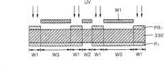
图11A至11I图示了根据本发明的当前实施例的制造等离子体显示面板的方法。如图11A所示,制备第一电极板的原材料金属板,例如,可制备具有高电导率和高化学吸氧性的铝板330′。下一步,如图11B所示,第一光刻胶P1和第二光刻胶P2涂覆在铝板330′的上、下表面上。第一和第二光刻胶P1和P2可由光敏树脂材料形成,光敏树脂材料当暴露于例如紫外(UV)线的辐射光时固化。11A to 11I illustrate a method of manufacturing a plasma display panel according to the current embodiment of the present invention. As shown in FIG. 11A , to prepare the raw material metal plate of the first electrode plate, for example, an
随后,进行曝光处理,其中利用曝光掩膜M1对第一光刻胶P1选择性地照射UV线,并进行显影处理,然后,具有预定图样的第一PR掩膜(PR1)如图11C所示地形成。第一PR掩膜PR1具有对应于放电电极的W1部分的图样,并覆盖相应的W1部分。随后,利用曝光掩膜M2对第二光刻胶P2进行曝光和显影处理,然后,具有预定图样的第二PR掩膜(PR2)如图11D所示地形成。第二PR掩膜PR2具有对应于放电电极的W1部分的图样,并覆盖W1部分。形成在铝板330′上、下表面上的第一PR掩膜PR1和第二PR掩膜PR2可相互竖向对齐设置。在后文中进行描述的蚀刻处理中,利用第一和第二PR掩膜PR1和PR2从两表面蚀刻铝板330′以形成放电空间。此时,如果由于第一和第二PR掩膜PR1和PR2的不准确设置而产生对准偏差,则放电空间不一致,并且面板的显示功能可能恶化。Subsequently, an exposure process is performed in which the first photoresist P1 is selectively irradiated with UV rays using the exposure mask M1, and a development process is performed, and then the first PR mask (PR1) having a predetermined pattern is shown in FIG. 11C formed. The first PR mask PR1 has a pattern corresponding to the W1 portion of the discharge electrode and covers the corresponding W1 portion. Subsequently, the second photoresist P2 is exposed and developed using the exposure mask M2, and then, a second PR mask (PR2) having a predetermined pattern is formed as shown in FIG. 11D. The second PR mask PR2 has a pattern corresponding to the W1 portion of the discharge electrode, and covers the W1 portion. The first PR mask PR1 and the second PR mask PR2 formed on the upper and lower surfaces of the aluminum plate 330' may be vertically aligned with each other. In an etching process described later, the aluminum plate 330' is etched from both surfaces using first and second PR masks PR1 and PR2 to form discharge spaces. At this time, if an alignment deviation occurs due to inaccurate placement of the first and second PR masks PR1 and PR2, the discharge spaces are inconsistent, and the display function of the panel may be deteriorated.
如图11E和11F所示,铝板330′的上表面利用第一PR掩膜PR1作为阻蚀层进行蚀刻。放电空间的W3部分和在放电电极之间的W2部分被选择性地蚀刻。在这里,放电空间的W3部分全蚀刻,而在放电电极之间的W2部分半蚀刻。As shown in FIGS. 11E and 11F, the upper surface of the aluminum plate 330' is etched using the first PR mask PR1 as a resist. Portions W3 of the discharge space and portions W2 between the discharge electrodes are selectively etched. Here, part W3 of the discharge space is fully etched, and part W2 between the discharge electrodes is half etched.
另外,如图11E和11F所示,铝板330′的下表面利用第二PR掩膜PR2作为阻蚀层进行蚀刻。通过此蚀刻处理,放电空间的W3部分和在放电电极之间的W2部分被选择性地蚀刻。在这里,放电空间的W3部分全蚀刻,直至放电空间S被完全穿透,而放电电极之间的W2部分被半蚀刻,从而保持预定厚度。In addition, as shown in FIGS. 11E and 11F, the lower surface of the aluminum plate 330' is etched using the second PR mask PR2 as a resist. Through this etching process, the W3 portion of the discharge space and the W2 portion between the discharge electrodes are selectively etched. Here, the W3 portion of the discharge space is fully etched until the discharge space S is completely penetrated, and the W2 portion between the discharge electrodes is half-etched so as to maintain a predetermined thickness.
随后,将第一和第二掩膜PR1和PR2去除,然后,获得具有图11G的结构的电极板330。在上述蚀刻处理后保留的某些部分335′形成放电电极,其他部分331′在放电电极之间形成隔离层。Subsequently, the first and second masks PR1 and PR2 are removed, and then, the
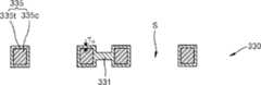
另外,如图11H所示,进行阳极化处理,用于在电极板330的表面上形成氧化物膜335t。沿电极板330的表面形成的氧化物膜335t由具有绝缘性能的陶瓷材料Al2O3形成。在这里,被形成为相对厚的放电电极335包括未被氧化以保留电导性能的核心部335c,并且,在放电电极之间形成为相对薄的部分被完全氧化并隔离,从而形成支撑放电电极335并将放电电极335相互隔离的隔离层331。阳极化处理是本发明的特征,并将在以后进行更详细的描述。In addition, as shown in FIG. 11H , anodization treatment is performed for forming an
另一方面,如图11I所示,具有与电极板330的结构大致相同的结构的另一电极板340可通过重复上述处理而获得。电极板340包括放电电极345之间的隔离层341,并且被氧化物膜345覆盖的每个放电电极345包括保持电导性能的核心部345c。随后,电极板330和340被相互对称设置,并利用隔离粘合剂365相互联结。然而,即使电极板330和340不利用粘合剂365直接相互联结,电极板330和340的堆叠结构也可通过前基板310与后基板320之间的联结力而保持,因此,粘合剂365不是必要特征。On the other hand, as shown in FIG. 11I , another
随后,制备将设置在电极板330和340的上、下表面上的前基板310和后基板320。前、后基板310和320可以是玻璃基板。另外,槽320′形成在后基板320上并在其间具有恒定间隔,荧光物325应用在槽320′上。槽320′对应于形成在电极板330和340中的放电空间S。然后,前、后基板310和320被相互垂直设置,同时将电极板330和340插于其间,然后,前、后基板310和320利用应用在基板310与320之间的熔接(frit)密封材料315相互联结。Subsequently, the
在下文中,本发明的阳极化处理将更详细地描述。图12示意性图示了阳极化处理。在本发明的阳极化处理中,在例如硼酸铵、磷酸铵或酒石酸铵的电解溶剂中,铝板(Al)为阳极(+),而例如Pb、碳、Ni和作为催化剂的Pb的材料为阴极。在这些条件下,提供DC电流以发生电-化学反应,用于沿Al板表面形成氧化物膜Al2O3。氧化物膜的厚度通过调整例如处理时间或DC电流量的处理条件而可最佳地控制在例如1μm至50μm的范围内。Hereinafter, the anodizing treatment of the present invention will be described in more detail. Figure 12 schematically illustrates anodization. In the anodizing process of the present invention, in an electrolytic solvent such as ammonium borate, ammonium phosphate or ammonium tartrate, an aluminum plate (Al) is an anode (+), and a material such as Pb, carbon, Ni, and Pb as a catalyst is a cathode . Under these conditions, a DC current was supplied to cause an electrochemical reaction for forming an oxide film Al2 O3 along the surface of the Al plate. The thickness of the oxide film can be optimally controlled within a range of, for example, 1 μm to 50 μm by adjusting treatment conditions such as treatment time or amount of DC current.
图13是显示氧化物膜的竖直横截面的示意图。氧化物膜通常包括具有相互不同膜特性的两个薄膜。多孔层包括具有几nm至100nm直径的纳米孔,并形成在氧化物膜的外表面部分上。因此,多孔层具有相对低的电绝缘性能。阻隔层形成在多孔层与在多孔层下的Al金属之间,并且阻隔层具有无孔的致密结构,从而有助于改善耐受电压。整个氧化物膜的耐受电压取决于阻隔层的厚度,然而,在利用硫磺酸或草酸作为电解溶剂的传统阳极化处理中,阻隔层的最大厚度为大约0.1μm。FIG. 13 is a schematic diagram showing a vertical cross-section of an oxide film. An oxide film generally includes two thin films having mutually different film properties. The porous layer includes nanopores having a diameter of several nm to 100 nm, and is formed on the outer surface portion of the oxide film. Therefore, the porous layer has relatively low electrical insulating properties. The barrier layer is formed between the porous layer and the Al metal under the porous layer, and the barrier layer has a non-porous dense structure, thereby contributing to an improvement in withstand voltage. The withstand voltage of the entire oxide film depends on the thickness of the barrier layer, however, in conventional anodization using sulfuric acid or oxalic acid as an electrolytic solvent, the maximum thickness of the barrier layer is about 0.1 μm.
在本发明中,使用例如硼酸铵、磷酸铵、或酒石酸铵的中性电解溶剂,因此,可形成厚的阻隔层。当在阳极化处理中应用700V的电压时,可形成具有1μm厚度的阻隔层。图14的电子显微照片显示了通过本发明的阳极化处理获得的氧化物膜的竖直横截面。如图14所示,阻隔层的厚度增大,并且,通过本发明的阳极化处理可形成最大厚度为1μm的阻隔层。In the present invention, a neutral electrolytic solvent such as ammonium borate, ammonium phosphate, or ammonium tartrate is used, and thus, a thick barrier layer can be formed. When a voltage of 700V was applied in anodizing, a barrier layer having a thickness of 1 μm could be formed. FIG. 14 is an electron micrograph showing a vertical cross-section of an oxide film obtained by anodization of the present invention. As shown in FIG. 14, the thickness of the barrier layer was increased, and a barrier layer with a maximum thickness of 1 μm could be formed by the anodization treatment of the present invention.
根据本发明,作为电介质层的氧化物膜通过使其上形成有放电电极图样的金属板氧化而形成在放电电极的表面上,因此,不需要另外的处理以形成电介质层。具体地,提供具有新结构并适于批量生产的等离子体显示面板,其中,电极延伸并同时围绕放电空间,因此,可克服传统的高效显示面板的限制,并可使显示面板商业化。According to the present invention, an oxide film as a dielectric layer is formed on the surface of the discharge electrode by oxidizing the metal plate on which the discharge electrode pattern is formed, and therefore, no additional treatment is required to form the dielectric layer. In particular, a plasma display panel having a new structure suitable for mass production is provided, in which electrodes extend while surrounding a discharge space, and thus, limitations of conventional high-efficiency display panels can be overcome and the display panel can be commercialized.
另外,电连接部分和隔离部分的厚度或宽度被设置为相互不同,因此,可以进行相同的氧化处理,而不需要用于进行选择性氧化处理的另外的图样处理,以形成导电部分和隔离部分。因此,制造过程可最小化。In addition, the thickness or width of the electrical connection portion and the isolation portion are set to be different from each other, therefore, the same oxidation treatment can be performed without additional pattern processing for performing selective oxidation treatment to form the conductive portion and the isolation portion . Therefore, the manufacturing process can be minimized.
具体地,根据本发明,圆形弯曲部分形成在放电电极的接触放电空间的拐角上,以防止氧化物膜的生长基底变弱,并在放电电极的包括拐角的整个表面上均匀形成氧化物膜。因此,可预先防止由于氧化物膜中的裂缝或具有稀疏结构的氧化物膜所致的放电稳定性和耐久性的降低。Specifically, according to the present invention, a circular curved portion is formed on the corner of the discharge electrode contacting the discharge space to prevent the growth substrate of the oxide film from weakening and to uniformly form the oxide film on the entire surface of the discharge electrode including the corner . Therefore, reduction in discharge stability and durability due to cracks in the oxide film or an oxide film having a sparse structure can be prevented in advance.
虽然本发明参照其示例性实施例进行了详细的显示和描述,然而本领域普通技术人员应理解的是,在不脱离由所附权利要求所限定的本发明的精神和范围的情况下,可在形式上和细节上进行各种修改。While the present invention has been shown and described in detail with reference to exemplary embodiments thereof, it will be understood by those of ordinary skill in the art that other modifications may be made without departing from the spirit and scope of the invention as defined by the appended claims. Various modifications have been made in form and detail.
Claims (29)
Translated fromChineseApplications Claiming Priority (2)
| Application Number | Priority Date | Filing Date | Title |
|---|---|---|---|
| KR1020070027819AKR100838083B1 (en) | 2007-03-21 | 2007-03-21 | Manufacturing method of plasma display panel and plasma display panel |
| KR10-2007-0027819 | 2007-03-21 |
Publications (1)
| Publication Number | Publication Date |
|---|---|
| CN101276721Atrue CN101276721A (en) | 2008-10-01 |
Family
ID=39591149
Family Applications (1)
| Application Number | Title | Priority Date | Filing Date |
|---|---|---|---|
| CNA2008100845197APendingCN101276721A (en) | 2007-03-21 | 2008-03-21 | Plasma display panel and manufacturing method thereof |
Country Status (5)
| Country | Link |
|---|---|
| US (1) | US20080231187A1 (en) |
| EP (1) | EP1973137A3 (en) |
| JP (1) | JP2008235274A (en) |
| KR (1) | KR100838083B1 (en) |
| CN (1) | CN101276721A (en) |
Families Citing this family (3)
| Publication number | Priority date | Publication date | Assignee | Title |
|---|---|---|---|---|
| KR100836428B1 (en)* | 2007-04-06 | 2008-06-09 | 삼성에스디아이 주식회사 | Electrode sheet for plasma display panel and plasma display panel using same |
| WO2008153663A1 (en)* | 2007-05-16 | 2008-12-18 | The Board Of Trustees Of The University Of Illinois | Arrays of microcavity plasma devices and electrodes with reduced mechanical stress |
| US8547004B2 (en)* | 2010-07-27 | 2013-10-01 | The Board Of Trustees Of The University Of Illinois | Encapsulated metal microtip microplasma devices, arrays and fabrication methods |
Family Cites Families (11)
| Publication number | Priority date | Publication date | Assignee | Title |
|---|---|---|---|---|
| DE1764261B2 (en)* | 1967-06-01 | 1976-05-26 | N.V. Philips' Gloeilampenfabrieken, Eindhoven (Niederlande) | GAS DISCHARGE DEVICE WITH TWO PARALLEL SYSTEMS OF LONG ELECTRODES THAT CROSS VERTICAL |
| DE2412869C3 (en)* | 1974-03-18 | 1980-10-30 | Siemens Ag, 1000 Berlin Und 8000 Muenchen | Display device with a gas discharge space as electron source, with an electron post-acceleration space and with a luminescent screen and method for operating this display device |
| JPH0770289B2 (en)* | 1991-11-29 | 1995-07-31 | 株式会社ティーティーティー | Display discharge tube |
| JP3891811B2 (en)* | 2001-10-02 | 2007-03-14 | 株式会社ノリタケカンパニーリミテド | AC type gas discharge display device and manufacturing method thereof |
| KR100922745B1 (en) | 2004-04-27 | 2009-10-22 | 삼성에스디아이 주식회사 | Plasma display panel |
| KR100768188B1 (en)* | 2005-07-04 | 2007-10-18 | 삼성에스디아이 주식회사 | Plasma display panel |
| KR100768222B1 (en)* | 2006-04-11 | 2007-10-18 | 삼성에스디아이 주식회사 | Plasma Display Panel And Method Of Manufacturing The Same |
| KR20080032443A (en)* | 2006-10-09 | 2008-04-15 | 삼성에스디아이 주식회사 | Plasma Display Panel And Method Of Manufacturing The Same |
| KR100829747B1 (en)* | 2006-11-01 | 2008-05-15 | 삼성에스디아이 주식회사 | Plasma display panel |
| KR100829746B1 (en)* | 2006-11-01 | 2008-05-19 | 삼성에스디아이 주식회사 | Plasma display device and manufacturing method thereof |
| KR100857070B1 (en)* | 2007-03-13 | 2008-09-05 | 엘지전자 주식회사 | Plasma display panel |
- 2007
- 2007-03-21KRKR1020070027819Apatent/KR100838083B1/ennot_activeExpired - Fee Related
- 2008
- 2008-03-19USUS12/077,867patent/US20080231187A1/ennot_activeAbandoned
- 2008-03-19JPJP2008072123Apatent/JP2008235274A/ennot_activeWithdrawn
- 2008-03-20EPEP08102806Apatent/EP1973137A3/ennot_activeWithdrawn
- 2008-03-21CNCNA2008100845197Apatent/CN101276721A/enactivePending
Also Published As
| Publication number | Publication date |
|---|---|
| KR100838083B1 (en) | 2008-06-16 |
| EP1973137A3 (en) | 2010-03-03 |
| JP2008235274A (en) | 2008-10-02 |
| EP1973137A2 (en) | 2008-09-24 |
| US20080231187A1 (en) | 2008-09-25 |
Similar Documents
| Publication | Publication Date | Title |
|---|---|---|
| US20080084154A1 (en) | Plasma display panel and method of manufacturing the same | |
| CN101276721A (en) | Plasma display panel and manufacturing method thereof | |
| KR100626001B1 (en) | Plasma Display Panel And Method Of Manufacturing The Same | |
| CN100520869C (en) | Plasma display module and method of manufacturing the same | |
| JP2006032341A (en) | Plasma display panel, plasma display panel manufacturing method, flat lamp, flat lamp manufacturing method | |
| JPH01115033A (en) | Gas discharge display device | |
| KR100829747B1 (en) | Plasma display panel | |
| EP1918961B1 (en) | Plasma display apparatus and manufacturing method of the same | |
| US20090091236A1 (en) | Plasma display panel having alignment structures and method of fabricating the same | |
| KR100578863B1 (en) | Plasma Display Panel with Improved Bus Electrode | |
| KR20010014721A (en) | Flat display device and fabricating method of the same | |
| KR100763392B1 (en) | Plasma display panel and manufacturing method thereof | |
| US20060220517A1 (en) | Display device | |
| KR100634710B1 (en) | Manufacturing Method of Plasma Display Panel | |
| US20070046206A1 (en) | Direct current plasma panel (DC-PDP) and method of manufacturing the same | |
| CN100378895C (en) | Method for manufacturing asymmetric barrier wall structure of plasma display | |
| CN101807503A (en) | plasma display panel | |
| JP4179345B2 (en) | Method for manufacturing plasma display panel | |
| KR100674870B1 (en) | Electrode Formation Method of Plasma Display Panel | |
| JP3539078B2 (en) | Method for manufacturing rear substrate for plasma display panel | |
| EP1840927A2 (en) | Plasma display panel and manufacturing method thereof | |
| KR100703093B1 (en) | Plasma display panel having an electrode inside the partition wall and a method of manufacturing the partition wall | |
| US20090153017A1 (en) | Plasma display panel and method of manufacturing the same | |
| KR100649202B1 (en) | Plasma display panel | |
| CN1838363A (en) | Plasma display panel and manufacturing method thereof |
Legal Events
| Date | Code | Title | Description |
|---|---|---|---|
| C06 | Publication | ||
| PB01 | Publication | ||
| C10 | Entry into substantive examination | ||
| SE01 | Entry into force of request for substantive examination | ||
| C02 | Deemed withdrawal of patent application after publication (patent law 2001) | ||
| WD01 | Invention patent application deemed withdrawn after publication | Open date:20081001 |