CN101276639B - Memory and how it works - Google Patents
Memory and how it worksDownload PDFInfo
- Publication number
- CN101276639B CN101276639BCN200710090629XACN200710090629ACN101276639BCN 101276639 BCN101276639 BCN 101276639BCN 200710090629X ACN200710090629X ACN 200710090629XACN 200710090629 ACN200710090629 ACN 200710090629ACN 101276639 BCN101276639 BCN 101276639B
- Authority
- CN
- China
- Prior art keywords
- memory
- interval time
- group
- memory group
- row
- Prior art date
- Legal status (The legal status is an assumption and is not a legal conclusion. Google has not performed a legal analysis and makes no representation as to the accuracy of the status listed.)
- Active
Links
- 238000000034methodMethods0.000claimsabstractdescription16
- 239000002699waste materialSubstances0.000abstractdescription4
- 230000005055memory storageEffects0.000description33
- 102100026620E3 ubiquitin ligase TRAF3IP2Human genes0.000description11
- 101710140859E3 ubiquitin ligase TRAF3IP2Proteins0.000description11
- 238000010586diagramMethods0.000description10
- 101000908384Bos taurus Dipeptidyl peptidase 4Proteins0.000description4
- HEFNNWSXXWATRW-UHFFFAOYSA-NIbuprofenChemical compoundCC(C)CC1=CC=C(C(C)C(O)=O)C=C1HEFNNWSXXWATRW-UHFFFAOYSA-N0.000description4
- 238000011017operating methodMethods0.000description4
- 230000008569processEffects0.000description3
- 230000001960triggered effectEffects0.000description3
- 101150024393ACT5 geneProteins0.000description2
- 101100492334Saccharomyces cerevisiae (strain ATCC 204508 / S288c) ARP1 geneProteins0.000description2
- 101150079344ACT4 geneProteins0.000description1
- 101100498818Arabidopsis thaliana DDR4 geneProteins0.000description1
- 101100056774Saccharomyces cerevisiae (strain ATCC 204508 / S288c) ARP3 geneProteins0.000description1
- 238000012986modificationMethods0.000description1
- 230000004048modificationEffects0.000description1
- 230000004044responseEffects0.000description1
- 238000010187selection methodMethods0.000description1
- 239000004065semiconductorSubstances0.000description1
Images


Landscapes
- Dram (AREA)
Abstract
Description
Translated fromChinese技术领域technical field
本发明是关于一种记忆体,且特别是关于一种具有不同行对行延迟时间(row to row delay,以下简称tRRD时间)的动态随机选择记忆体(Dynamicrandom access memory,DRAM)与其操作方法。The present invention relates to a memory, and in particular to a dynamic random access memory (DRAM) with different row-to-row delay times (tRRD time for short) and its operating method.
背景技术Background technique
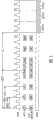
现有习知的半导体记忆元件通常包括多个记忆储存库(bank),其中每个记忆储存库具有相同的容量(也就是记忆胞的数目相同)及相同的储存容量。特别是,现在一般用于动态随机选择记忆体(dynamic random accessmemory,简称DRAM)的标准记忆体架构,通常包括多个相等容量的记忆储存库(bank)。如图1所示,图1为根据现有习知技术的DRAM架构图。记忆体100包括记忆单元110与驱动电源120,其中记忆单元110包括记忆储存库101~108,当系统选择记忆体100中的行(Row)时,则由驱动电源120提供电压来驱动相对应的电路。Conventional semiconductor memory devices generally include a plurality of memory banks, wherein each memory bank has the same capacity (that is, the same number of memory cells) and the same storage capacity. In particular, the standard memory architecture generally used for dynamic random access memory (DRAM) generally includes a plurality of memory storage banks (banks) of equal capacity. As shown in FIG. 1 , FIG. 1 is a DRAM architecture diagram according to the prior art. The memory 100 includes a memory unit 110 and a driving power supply 120, wherein the memory unit 110 includes memory storage banks 101-108. When the system selects a row (Row) in the memory 100, the driving power supply 120 provides a voltage to drive the corresponding circuit.
当记忆体100接收到有效命令信号(Active)时,位址缓冲器(Addressbuffer)接收系统所输入的位址,然后经由行位址产生器产生行位址(Rowaddress)。记忆体100便根据行位址至相对应的记忆储存库101~108中读取资料。由于DRAM的操作频率很快,单一驱动电源120的驱动能力无法马上提供操作下一行所需的电流。所以系统需要间隔一段时间才能再输出下一个有效命令信号,让驱动电源120有恢复驱动电压的时间,这也就是一般DRAM规格上的tRRD时间。而在现有习知技术中,不论是在同一个记忆储存库101~108或是在不同记忆储存库101~108(例如由记忆储存库101转换到记忆储存库102)的操作过程,其tRRD时间都是固定的。因此,当tRRD>tCCD(资料读取的间隔时间)时,记忆体100便无法连续读取资料,而造成资料空隙。When the memory 100 receives an active command signal (Active), the address buffer (Addressbuffer) receives the address input by the system, and then generates a row address (Rowaddress) through the row address generator. The memory 100 reads data from the corresponding memory storage banks 101 - 108 according to the row address. Since the operating frequency of the DRAM is very fast, the driving capability of the single driving power supply 120 cannot immediately provide the current required to operate the next row. Therefore, the system needs a period of time before outputting the next effective command signal, so that the driving power supply 120 has time to restore the driving voltage, which is the tRRD time in the general DRAM specification. However, in the prior art, whether it is in the same memory storage bank 101-108 or in the operation process of different memory storage banks 101-108 (for example, switching from the
图2为根据现有习知技术的时钟波形图。以下说明请同时参考图1。有效命令信号ACT1、ACT2分别对应于记忆储存库101、102,而有效命令信号ACT1与ACT2之间的间隔时间为tRRD时间(图2中为4个时钟周期)。以记忆储存库101为例,有效命令信号ACT1与读取命令Read1之间需要间隔行对列延迟时间tRCD(RAS to CAS delay,以下简称tRCD时间)(图2中为7个时钟周期),从接收读取命令Read1到输出所读取的资料至汇流排需要延迟时间CL(7个时钟周期)。记忆储存库102的读取流程亦相同,在此不加累述。FIG. 2 is a clock waveform diagram according to the prior art. Please also refer to Figure 1 for the following description. The active command signals ACT1 and ACT2 correspond to the
由于有效命令信号ACT1、ACT2之间需要相差4个时钟周期(tRRD的时间长度),因此读取命令Read1、Read2输出的时间也会相差4个时钟。同理,记忆体110不论在同一个记忆储存库101~108或是不同记忆储存库101~108之中读取资料,皆会因为行对行延迟时间tRRD大于tCCD而产生资料空隙BUBBLE,造成读取效率下降,浪费系统资源。Since the effective command signals ACT1 and ACT2 need to differ by 4 clock cycles (the time length of tRRD), the output time of the read commands Read1 and Read2 will also differ by 4 clock cycles. Similarly, no matter whether the memory 110 reads data from the same memory storage bank 101-108 or different memory storage banks 101-108, there will be a data gap BUBBLE because the row-to-row delay time tRRD is greater than tCCD, resulting in a read Fetch efficiency drops and system resources are wasted.
发明内容Contents of the invention
本发明提出一种记忆体,利用不同的tRRD时间,让记忆体可利用较短的时间间隔,选取位于不同的记忆组中的行,以增加资料选择的效率。The present invention proposes a memory that utilizes different tRRD times to allow the memory to select rows located in different memory groups at shorter time intervals, so as to increase the efficiency of data selection.
本发明提出一种记忆体,将记忆储存库分为不同记忆组,每一记忆组设置独立的驱动电源,以降低记忆组之间的tRRD时间,使资料的选择更快速。The present invention proposes a memory, which divides the memory bank into different memory groups, and each memory group is provided with an independent driving power supply, so as to reduce the tRRD time between the memory groups and make data selection faster.
本发明提出一种记忆体的操作方法,利用不同的tRRD时间,让记忆体可以利用较短的tRRD时间,选择不同的记忆组中的行以读取资料,进而减少资料空隙的产生。The present invention proposes a method for operating a memory, using different tRRD times, so that the memory can use a shorter tRRD time to select rows in different memory groups to read data, thereby reducing the generation of data gaps.
本发明提出一种记忆体,包括第一记忆组、第二记忆组,其中第一记忆组具有多个第一记忆储存库,第二记忆组具有多个第二记忆储存库。其中,记忆体选择第一记忆组与第二记忆组中的行的最小间隔时间为一外部间隔时间,而选择第一记忆组的一行至选择第一记忆组中的另一行或选择第二记忆组中的一行至选择第二记忆组中的另一行的最小间隔时间为一内部间隔时间,其中外部间隔时间小于内部间隔时间。The present invention proposes a memory including a first memory group and a second memory group, wherein the first memory group has a plurality of first memory banks, and the second memory group has a plurality of second memory banks. Wherein, the memory selects the minimum interval time between the rows in the first memory group and the second memory group as an external interval time, and selects one row in the first memory group to selects another row in the first memory group or selects the second memory group. The minimum interval time between one row in the group and selecting another row in the second memory group is an internal interval time, wherein the external interval time is smaller than the internal interval time.
在本发明另一实施例中,上述记忆体根据第一有效命令信号,选择第一记忆组中的第一记忆储存库中的一行,以及根据第二有效命令信号,选择第二记忆组中的第二记忆储存库中的一行,其中第一有效命令信号与第二有效命令信号的最小间隔时间等于外部间隔时间。且若记忆体选择第一记忆组的一行,则在间隔外部间隔时间后,可选择第二记忆组的另一行。In another embodiment of the present invention, the above-mentioned memory selects a row in the first memory bank in the first memory group according to the first valid command signal, and selects a row in the second memory bank according to the second valid command signal. A row in the second memory bank, wherein the minimum interval time between the first valid command signal and the second valid command signal is equal to the external interval time. And if the memory selects one row of the first memory group, another row of the second memory group can be selected after an external interval time.
在本发明另一实施例中,记忆体更包括第一驱动电源以及第二驱动电源,其中第一驱动电源提供第一操作电压至第一记忆组;以及第二驱动电源提供第二操作电压至第二记忆组。In another embodiment of the present invention, the memory further includes a first driving power supply and a second driving power supply, wherein the first driving power supply provides a first operating voltage to the first memory group; and the second driving power supply provides a second operating voltage to Second memory group.
从另一个观点来看,本发明提出一种记忆体的操作方法,包括下列步骤:首先,根据第一有效命令信号,选择第一记忆组中的一行,以及根据第二有效命令信号,选择第二记忆组中的一行,其中第二有效命令信号与第一有效命令信号的输出时间最小相距一外部间隔时间。然后,根据第三有效命令信号,选择第一记忆组中的另一行,其中第三有效命令信号与第一有效命令信号的输出时间最小相距一内部间隔时间,而其外部间隔时间小于内部间隔时间。From another point of view, the present invention proposes a method for operating a memory, which includes the following steps: first, select a row in the first memory group according to the first valid command signal, and select a row in the first memory group according to the second valid command signal. One row in the two memory groups, wherein the output time of the second valid command signal and the first valid command signal is at least an external interval time apart. Then, select another row in the first memory group according to the third valid command signal, wherein the output time of the third valid command signal and the first valid command signal is at least one internal interval time apart, and its external interval time is less than the internal interval time .
在本发明一实施例中,上述第一记忆组包括多个第一记忆储存库,第二记忆组包括多个第二记忆储存库。且本发明的记忆体的操作方法,更包括下列步骤:首先,设置第一驱动电源,用以提供第一操作电压至第一记忆组;以及设置第二驱动电源,用以提供第二操作电压至第二记忆组。In an embodiment of the present invention, the first memory group includes a plurality of first memory banks, and the second memory group includes a plurality of second memory banks. And the operation method of the memory of the present invention further includes the following steps: first, setting the first driving power supply to provide the first operating voltage to the first memory group; and setting the second driving power supply to provide the second operating voltage to the second memory group.
综合上述,本发明利用不同的tRRD时间,提高记忆体的资料读取速度以及减少资料空隙的产生。另外,本发明将记忆储存库分为不同的记忆组,分别设置不同的驱动电源,用来提高记忆体的反应速度以降低tRRD时间的长度。利用本发明的记忆体架构与选择方法,可提升记忆体的资料读取速度,降低资料空隙的产生,避免系统资料的浪费。Based on the above, the present invention uses different tRRD times to increase the data reading speed of the memory and reduce the occurrence of data gaps. In addition, the present invention divides the memory storage bank into different memory groups, and sets different driving power sources respectively, so as to increase the response speed of the memory and reduce the length of tRRD time. By using the memory structure and selection method of the present invention, the data reading speed of the memory can be increased, the generation of data gaps can be reduced, and the waste of system data can be avoided.
为让本发明的上述和其他目的、特征和优点能更明显易懂,下文特举本发明的较佳实施例,并配合所附图式,作详细说明如下。In order to make the above and other objects, features and advantages of the present invention more comprehensible, preferred embodiments of the present invention will be described in detail below together with the accompanying drawings.
附图说明Description of drawings
图1为根据现有习知技术的DRAM架构图。FIG. 1 is a structure diagram of a DRAM according to the prior art.
图2为根据现有习知技术的时钟波形图。FIG. 2 is a clock waveform diagram according to the prior art.
图3为根据本发明一实施例的记忆体架构图。FIG. 3 is a memory architecture diagram according to an embodiment of the invention.
图4为根据本发明另一实施例的记忆体架构图。FIG. 4 is a memory architecture diagram according to another embodiment of the present invention.
图5为根据本发明另一实施例的时钟波形图。FIG. 5 is a clock waveform diagram according to another embodiment of the present invention.
图6为根据本发明另一实施例的记忆体的操作方法的流程图。FIG. 6 is a flowchart of a memory operating method according to another embodiment of the invention.
100、300、400:记忆体 110:记忆单元100, 300, 400: memory 110: memory unit
120、330、340、415、425、435、445:驱动电源120, 330, 340, 415, 425, 435, 445: drive power
101~108、A301~A304:记忆储存库101~108, A301~A304: memory storage
B301~304、A401~A404:记忆储存库B301~304, A401~A404: memory storage
B401~B404、C401~C404:记忆储存库B401~B404, C401~C404: memory storage
D401~D404:记忆储存库D401~D404: Memory repository
310、320、410~440:记忆组310, 320, 410~440: memory group
ACT1~ACT5:有效命令信号ACT1~ACT5: valid command signal
tRRD:行对行延迟时间 tRCD:行对列延迟时间tRRD: row-to-row delay time tRCD: row-to-column delay time
tRRD-inter:外部间隔时间 tRRD-intra:内部间隔时间tRRD-inter: external interval time tRRD-intra: internal interval time
Read1~Read4:读取命令 BUBBLE:资料空隙Read1~Read4: Read command BUBBLE: Data gap
CL:延迟时间 S610~S630:步骤CL: delay time S610~S630: steps
具体实施方式Detailed ways
图3为根据本发明一实施例的记忆体架构图,记忆体300包括驱动电源330、340、记忆组310、320,其中驱动电源330耦接于记忆组310,而驱动电源340耦接于记忆组320。记忆组310包括记忆储存库A301~A304,而记忆组320包括记忆储存库B301~B304。换言之,记忆体300将记忆储存库A301~A304、B301~304分为两组,分别配置不同的驱动电源330、340以即时提供记忆体300所需操作电压。驱动电源330、340为独立的电压源,但其电源线可以相连或是独立。当记忆体300需要读取记忆储存库A301~A304中的资料时,由驱动电源330提供操作电压至相对应的记忆储存库A301~A304中的记忆胞(memory cell)以进行选择与存取(Active、Read/Write)的动作。3 is a memory architecture diagram according to an embodiment of the present invention. The
记忆体300可由多个行(ROW)与多个列(Column)的位址来划分各个记忆胞的位置,藉由选择不同位址的行与列,即可读取不同记忆胞的资料。而在本实施例中,记忆体300选择记忆组310的一行到记忆组320中的行的最小间隔时间为外部间隔时间(tRRD-inter),而选择位于同一记忆组中的一行到同一记忆组中的下一行(如310或320)中的行的最小间隔时间为一内部间隔时间(tRRD-intra),其中外部间隔时间小于内部间隔时间。换言之,有效命令信号的输出间隔分为两种间隔时间,分别为外部间隔时间与内部间隔时间。内部间隔时间为重复在同一记忆组中打开(或是选择)行的最小间隔时间,而外部间隔时间则表示在不同记忆组之间打开(或是选择)不同行的最小间隔时间。The
举例来说,若记忆体300根据第一有效命令信号,选择记忆组310中的记忆储存库A301~A304中的一行,然后根据第二有效命令信号,选择记忆组320中的记忆储存库B301~B304中的一行,则第一有效命令信号与第二有效命令信号的最小间隔时间等于外部间隔时间。而当记忆体300根据第三有效命令信号,再度读取记忆组310中的记忆储存库A301~A304其中的一行时,则第三有效命令信号与第一有效命令的最小间隔时间为内部间隔时间。For example, if the
由于记忆体300是依照所接收的有效命令信号来进行资料的读取,因此每一个有效命令信号都会对应于记忆体组310或320中的一行。为避免资料输出产生空档,也就是资料空隙的产生。记忆体300利用间隔读出的方式来读取资料,记忆体300先从记忆组310中的记忆组储存库A301~A304中读取资料,然后,转换至记忆组320中的记忆组储存库B301~B304中读取下笔资料。由于外部间隔时间小于内部间隔时间,因此,藉由转换不同记忆组310、320来读取资料会比在同一组记忆组310或320中连续读取两笔资料的速度较快。Since the
换言之,在本实施例中,记忆体300若先由记忆组310读取资料,则下一笔资料会经由记忆组310以外的记忆组(也就是记忆组320)来读取。以有效命令信号的角度来看,则若第一个有效命令信号对应于记忆组310中的记忆储存库A301~A304,则下一个有效命令信号则对应于记忆组310以外的记忆组(也就是记忆组320)。In other words, in this embodiment, if the
在现有习知的记忆体架构中,并没有记忆储存库分组的概念,且受限于驱动电源的驱动能力与速度,所以行对行的间隔时间均为固定,资料读出的时候容易产生资料空隙,造成系统运算资源的浪费。在本实施例中,记忆体300具有两个驱动电源330、340,分别负责提供操作电压至记忆组310、320。由于驱动电源330、340互为独立,不受前一次驱动的影响,所以外部间隔时间可以小于内部间隔时间。比较现有习知单一驱动电源的系统架构,独立的驱动电源330、340可以让操作电压的提供速度更快。In the existing conventional memory architecture, there is no concept of memory bank grouping, and it is limited by the driving capability and speed of the driving power supply, so the row-to-row interval is fixed, and it is easy to generate data when reading data. Data gaps cause waste of system computing resources. In this embodiment, the
在本发明另一实施例中,本发明也可以将记忆储存库分为多组,如图4所示,图4为根据本发明另一实施例的记忆体架构图。记忆体400包括记忆组410~440、驱动电源415、425、435、445,其中记忆组410包括记忆储存库A401~A404,记忆组420包括记忆储存库B401~B404,记忆组430包括记忆储存库C401~C404,记忆组430包括记忆储存库D401~D404。记忆体400选择记忆组410~440中任两组中的行到另一组中的行的最小间隔时间为外部间隔时间,而选择记忆组410~440任一组中的记忆储存库的行至同一记忆组的另一行的时间间隔为内部间隔时间。若记忆体400根据有效命令信号ACT1(请参照图5)选择记忆组410中的记忆储存库A401~A404,则可根据下一个有效命令信号,选择记忆组420、430、440其中一个。然后,记忆体400可回到记忆组410再选择另一行。换言之,记忆体400可切换记忆组410~440来增加记忆储存库选择与资料读出的速度,以避免资料空隙的产生。图4实施例中其余操作细节请参照上述图3的说明,在此不加累述。In another embodiment of the present invention, the present invention can also divide the memory storage into multiple groups, as shown in FIG. 4 , which is a memory architecture diagram according to another embodiment of the present invention.
图5为根据本发明另一实施例的时钟波形图,以下说明请同时参照图3。有效命令信号ACT1(位于第0个时钟)对应于记忆组310中的记忆储存库A301,有效命令信号ACT2(位于第2个时钟)对应于记忆组320中的记忆储存库B301,其中有效命令信号ACT1与有效命令信号ACT2间隔一外部间隔时间tRRD-inter(本实施例中为2个时钟周期)。有效命令信号ACT3(位于第4个时钟)则对应于记忆组310中的记忆储存库A302,其中有效命令信号ACT3与有效命令信号ACT1间隔4个时钟周期(本实施例中的内部间隔时间tRRD-intra为4个时钟周期,表示记忆体310选择同一记忆组的行到下一行的最小间隔时间大于4个时钟周期即可),这是因为记忆储存库A301、A302均属于同一个记忆组310之间的关系。FIG. 5 is a clock waveform diagram according to another embodiment of the present invention. Please refer to FIG. 3 for the following description. Effective command signal ACT1 (located at the 0th clock) corresponds to the memory storage bank A301 in the
在记忆体300接收有效命令信号后ACT1、ACT2或ACT3后经过tRCD时间(本实施例中为7个时钟周期)后,记忆体300可接受读取命令(Read)或是写入命令(Write),到对应的记忆储存库中读取或写入资料。因此,记忆体300根据有效命令信号ACT1,在第7个时钟触发时,可接受读取命令Read1至记忆储存库A301中读取资料;根据有效命令信号ACT2,在第9个时钟触发时,可接受另一读取命令Read2至记忆储存库B301读取资料;根据第三个有效命令信号ACT3在第11个时钟触发时,可接受读取命令Read3,然后至记忆体储存库A302中读取资料。而在读取命令之間的空档,记忆体300可再处理其余的有效命令信号(如ACT4、ACT5),使资料读出更有效率。利用本发明的选择与读取方法,可以让资料的输出更为紧凑,避免时钟的浪费。在本实施例中,由于外部间隔时间tRRD-inter仅需要2个时钟周期,因此,有效命令信号的最小间隔时间即可设为2个时钟周期,表示记忆体300每次读取资料的间隔最多只会有2个时钟周期。当然,在本发明另一实施例中,外部间隔时间tRRD-inter并不限制于上述2个时钟周期,亦可设计为单一时钟周期,只要配置适当的驱动电源即可。另外,记忆体的读取与储存的操作方式相似,本发明亦可应用于资料的写入。After the
当记忆体310接受对应的记忆储存库(如A301)的读取命令后,再经过延迟时间CL(本实施例中为7个时钟周期)后会输出所读取的资料至汇流排。如图5中的资料列所示,资料DATA1~DATA3会依序输出,且其中不会产生资料空隙,与现有习知的图2相比,即可明显看出其资料输出效率较高。此外,本发明可应用于DDR(double-data-rate)1~DDR4规格的动态随机选择记忆体(DRAM),因此,上述关于tRCD、tRRD、CL等时间规格不限定于上述实施例所提及的范围,在本技术领域具有通常知识者,经由本发明的揭露应可轻易推知其余应用的方式,在此不加累述。After the
图6为根据本发明另一实施例的记忆体的操作方法的流程图。以下说明请配合图3,首先,步骤S610根据第一有效命令信号,选择第一记忆组(例如记忆组310)中的行。然后,步骤S620根据第二有效命令信号,选择第二记忆组(例如记忆组320)中的行,其中第二有效命令信号与第一有效命令信号的输出时间最小相距一外部间隔时间。接下来,步骤S630根据第三有效命令信号,选择第一记忆组中的另一行,其中第三有效命令信号与第一有效命令信号的输出时间最小相距一内部间隔时间,其中外部间隔时间小于内部间隔时间。FIG. 6 is a flowchart of a memory operating method according to another embodiment of the invention. Please refer to FIG. 3 for the following description. First, step S610 selects a row in the first memory group (for example, the memory group 310 ) according to the first valid command signal. Then, step S620 selects a row in the second memory group (such as the memory group 320 ) according to the second valid command signal, wherein the output time of the second valid command signal and the first valid command signal are at least an external interval time apart. Next, step S630 selects another row in the first memory group according to the third valid command signal, wherein the output time of the third valid command signal and the output time of the first valid command signal is at least an internal interval time, wherein the external interval time is less than the internal interval time Intervals.
其中,接收有效命令信号的顺序,依序为第一有效命令信号、第二有效命令信号以及第三有效命令信号。且在本发明另一实施例中,上述的操作方法更包括下列步骤:设置第一驱动电源,用以提供操作电压至第一记忆组;以及设置第二驱动电源,用以提供操作电压至第二记忆组。上述记忆体的操作方法的其余操作细节请参照上述图3~图5的说明,在此不加累述。Wherein, the sequence of receiving the valid command signals is the first valid command signal, the second valid command signal and the third valid command signal. And in another embodiment of the present invention, the above-mentioned operating method further includes the following steps: setting a first driving power supply for providing an operating voltage to the first memory bank; and setting a second driving power supply for providing an operating voltage to the first memory bank Two memory groups. For the rest of the operation details of the operation method of the memory, please refer to the description of FIGS. 3 to 5 above, and will not be repeated here.
本发明将记忆储存库分为不同的记忆组,使其适用于不同的tRRD时间,加快记忆体在不同记忆组的间选择行与读取资料的速度以减少资料空隙的产生。The invention divides the memory storage bank into different memory groups, making it suitable for different tRRD times, and speeding up the speed of selecting rows and reading data between different memory groups to reduce the generation of data gaps.
虽然本发明已以较佳实施例揭露如上,然其并非用以限定本发明,任何所属技术领域具有通常知识者,在不脱离本发明的精神和范围内,当可作些许的更动与润饰,因此本发明的保护范围当视后附的申请专利范围所界定者为准。Although the present invention has been disclosed above with preferred embodiments, it is not intended to limit the present invention. Anyone with ordinary knowledge in the technical field may make some changes and modifications without departing from the spirit and scope of the present invention. Therefore, the scope of protection of the present invention should be defined by the scope of the appended patent application.
Claims (11)
Priority Applications (1)
| Application Number | Priority Date | Filing Date | Title |
|---|---|---|---|
| CN200710090629XACN101276639B (en) | 2007-03-30 | 2007-03-30 | Memory and how it works |
Applications Claiming Priority (1)
| Application Number | Priority Date | Filing Date | Title |
|---|---|---|---|
| CN200710090629XACN101276639B (en) | 2007-03-30 | 2007-03-30 | Memory and how it works |
Publications (2)
| Publication Number | Publication Date |
|---|---|
| CN101276639A CN101276639A (en) | 2008-10-01 |
| CN101276639Btrue CN101276639B (en) | 2010-10-27 |
Family
ID=39995956
Family Applications (1)
| Application Number | Title | Priority Date | Filing Date |
|---|---|---|---|
| CN200710090629XAActiveCN101276639B (en) | 2007-03-30 | 2007-03-30 | Memory and how it works |
Country Status (1)
| Country | Link |
|---|---|
| CN (1) | CN101276639B (en) |
Families Citing this family (2)
| Publication number | Priority date | Publication date | Assignee | Title |
|---|---|---|---|---|
| KR101092997B1 (en)* | 2009-12-14 | 2011-12-12 | 주식회사 하이닉스반도체 | Device for generating internal negative voltage |
| CN104821179B (en)* | 2015-04-16 | 2017-09-26 | 江苏时代全芯存储科技有限公司 | Memory body drive circuit |
Citations (1)
| Publication number | Priority date | Publication date | Assignee | Title |
|---|---|---|---|---|
| US6772352B1 (en)* | 2000-09-29 | 2004-08-03 | Intel Corporation | Method and apparatus for reducing the rate of commands being issued if the rate exceeds a threshold which is based upon a temperature curve |
- 2007
- 2007-03-30CNCN200710090629XApatent/CN101276639B/enactiveActive
Patent Citations (1)
| Publication number | Priority date | Publication date | Assignee | Title |
|---|---|---|---|---|
| US6772352B1 (en)* | 2000-09-29 | 2004-08-03 | Intel Corporation | Method and apparatus for reducing the rate of commands being issued if the rate exceeds a threshold which is based upon a temperature curve |
Also Published As
| Publication number | Publication date |
|---|---|
| CN101276639A (en) | 2008-10-01 |
Similar Documents
| Publication | Publication Date | Title |
|---|---|---|
| US9281047B2 (en) | Dynamic random access memory with fully independent partial array refresh function | |
| US8233347B2 (en) | Semiconductor memory, semiconductor device, and system | |
| US7301843B2 (en) | Semiconductor memory device having complete hidden refresh function | |
| US8325551B2 (en) | Semiconductor memory device using internal high power supply voltage in self-refresh operation mode and related method of operation | |
| CN1677562A (en) | semiconductor storage device | |
| JP2010170596A (en) | Semiconductor memory device | |
| US20030081492A1 (en) | Memory device operable in either a high-power, full-page size mode or a low-power, reduced-page size mode | |
| CN113140243A (en) | Word line driver circuit for memory device and method of operating the same | |
| TW200532687A (en) | Ripple refresh circuit and method for sequentially refreshing a semiconductor memory system | |
| JPH07130168A (en) | Semiconductor memory device | |
| JPH05266657A (en) | Dynamic semiconductor memory | |
| JP5710947B2 (en) | Semiconductor device and control method thereof | |
| KR20060027665A (en) | Semiconductor memory device having stack bank structure and word line driving method thereof | |
| JP2000156079A (en) | Semiconductor memory device having a multi-bank structure | |
| CN113016034A (en) | System and method for improving power efficiency in refreshing a memory bank | |
| US5875132A (en) | Semiconductor memory device for storing data comprising of plural bits and method for operating the same | |
| US6456563B1 (en) | Semiconductor memory device that operates in sychronization with a clock signal | |
| CN101276639B (en) | Memory and how it works | |
| US5517454A (en) | Semiconductor memory device having refresh circuits | |
| JP2006059490A (en) | Semiconductor memory device | |
| US7447102B2 (en) | Memory and operation method thereof | |
| CN116072169B (en) | Memory read-write circuit, memory control method and electronic equipment | |
| JP2009016004A (en) | Semiconductor device and control method of semiconductor device | |
| US7885126B2 (en) | Apparatus for controlling activation of semiconductor integrated circuit | |
| JP2012018711A (en) | Semiconductor device and control method thereof |
Legal Events
| Date | Code | Title | Description |
|---|---|---|---|
| C06 | Publication | ||
| PB01 | Publication | ||
| C10 | Entry into substantive examination | ||
| SE01 | Entry into force of request for substantive examination | ||
| C14 | Grant of patent or utility model | ||
| GR01 | Patent grant |