CN101273154A - Substrate processing method and recording medium - Google Patents
Substrate processing method and recording mediumDownload PDFInfo
- Publication number
- CN101273154A CN101273154ACNA2006800354936ACN200680035493ACN101273154ACN 101273154 ACN101273154 ACN 101273154ACN A2006800354936 ACNA2006800354936 ACN A2006800354936ACN 200680035493 ACN200680035493 ACN 200680035493ACN 101273154 ACN101273154 ACN 101273154A
- Authority
- CN
- China
- Prior art keywords
- film
- processing method
- substrate
- film formation
- temperature
- Prior art date
- Legal status (The legal status is an assumption and is not a legal conclusion. Google has not performed a legal analysis and makes no representation as to the accuracy of the status listed.)
- Pending
Links
Images


Classifications
- C—CHEMISTRY; METALLURGY
- C23—COATING METALLIC MATERIAL; COATING MATERIAL WITH METALLIC MATERIAL; CHEMICAL SURFACE TREATMENT; DIFFUSION TREATMENT OF METALLIC MATERIAL; COATING BY VACUUM EVAPORATION, BY SPUTTERING, BY ION IMPLANTATION OR BY CHEMICAL VAPOUR DEPOSITION, IN GENERAL; INHIBITING CORROSION OF METALLIC MATERIAL OR INCRUSTATION IN GENERAL
- C23C—COATING METALLIC MATERIAL; COATING MATERIAL WITH METALLIC MATERIAL; SURFACE TREATMENT OF METALLIC MATERIAL BY DIFFUSION INTO THE SURFACE, BY CHEMICAL CONVERSION OR SUBSTITUTION; COATING BY VACUUM EVAPORATION, BY SPUTTERING, BY ION IMPLANTATION OR BY CHEMICAL VAPOUR DEPOSITION, IN GENERAL
- C23C16/00—Chemical coating by decomposition of gaseous compounds, without leaving reaction products of surface material in the coating, i.e. chemical vapour deposition [CVD] processes
- C23C16/02—Pretreatment of the material to be coated
- C23C16/0227—Pretreatment of the material to be coated by cleaning or etching
- C—CHEMISTRY; METALLURGY
- C23—COATING METALLIC MATERIAL; COATING MATERIAL WITH METALLIC MATERIAL; CHEMICAL SURFACE TREATMENT; DIFFUSION TREATMENT OF METALLIC MATERIAL; COATING BY VACUUM EVAPORATION, BY SPUTTERING, BY ION IMPLANTATION OR BY CHEMICAL VAPOUR DEPOSITION, IN GENERAL; INHIBITING CORROSION OF METALLIC MATERIAL OR INCRUSTATION IN GENERAL
- C23C—COATING METALLIC MATERIAL; COATING MATERIAL WITH METALLIC MATERIAL; SURFACE TREATMENT OF METALLIC MATERIAL BY DIFFUSION INTO THE SURFACE, BY CHEMICAL CONVERSION OR SUBSTITUTION; COATING BY VACUUM EVAPORATION, BY SPUTTERING, BY ION IMPLANTATION OR BY CHEMICAL VAPOUR DEPOSITION, IN GENERAL
- C23C16/00—Chemical coating by decomposition of gaseous compounds, without leaving reaction products of surface material in the coating, i.e. chemical vapour deposition [CVD] processes
- C23C16/06—Chemical coating by decomposition of gaseous compounds, without leaving reaction products of surface material in the coating, i.e. chemical vapour deposition [CVD] processes characterised by the deposition of metallic material
- C23C16/16—Chemical coating by decomposition of gaseous compounds, without leaving reaction products of surface material in the coating, i.e. chemical vapour deposition [CVD] processes characterised by the deposition of metallic material from metal carbonyl compounds
- C—CHEMISTRY; METALLURGY
- C23—COATING METALLIC MATERIAL; COATING MATERIAL WITH METALLIC MATERIAL; CHEMICAL SURFACE TREATMENT; DIFFUSION TREATMENT OF METALLIC MATERIAL; COATING BY VACUUM EVAPORATION, BY SPUTTERING, BY ION IMPLANTATION OR BY CHEMICAL VAPOUR DEPOSITION, IN GENERAL; INHIBITING CORROSION OF METALLIC MATERIAL OR INCRUSTATION IN GENERAL
- C23C—COATING METALLIC MATERIAL; COATING MATERIAL WITH METALLIC MATERIAL; SURFACE TREATMENT OF METALLIC MATERIAL BY DIFFUSION INTO THE SURFACE, BY CHEMICAL CONVERSION OR SUBSTITUTION; COATING BY VACUUM EVAPORATION, BY SPUTTERING, BY ION IMPLANTATION OR BY CHEMICAL VAPOUR DEPOSITION, IN GENERAL
- C23C16/00—Chemical coating by decomposition of gaseous compounds, without leaving reaction products of surface material in the coating, i.e. chemical vapour deposition [CVD] processes
- C23C16/22—Chemical coating by decomposition of gaseous compounds, without leaving reaction products of surface material in the coating, i.e. chemical vapour deposition [CVD] processes characterised by the deposition of inorganic material, other than metallic material
- C23C16/30—Deposition of compounds, mixtures or solid solutions, e.g. borides, carbides, nitrides
- C23C16/34—Nitrides
- C—CHEMISTRY; METALLURGY
- C23—COATING METALLIC MATERIAL; COATING MATERIAL WITH METALLIC MATERIAL; CHEMICAL SURFACE TREATMENT; DIFFUSION TREATMENT OF METALLIC MATERIAL; COATING BY VACUUM EVAPORATION, BY SPUTTERING, BY ION IMPLANTATION OR BY CHEMICAL VAPOUR DEPOSITION, IN GENERAL; INHIBITING CORROSION OF METALLIC MATERIAL OR INCRUSTATION IN GENERAL
- C23C—COATING METALLIC MATERIAL; COATING MATERIAL WITH METALLIC MATERIAL; SURFACE TREATMENT OF METALLIC MATERIAL BY DIFFUSION INTO THE SURFACE, BY CHEMICAL CONVERSION OR SUBSTITUTION; COATING BY VACUUM EVAPORATION, BY SPUTTERING, BY ION IMPLANTATION OR BY CHEMICAL VAPOUR DEPOSITION, IN GENERAL
- C23C16/00—Chemical coating by decomposition of gaseous compounds, without leaving reaction products of surface material in the coating, i.e. chemical vapour deposition [CVD] processes
- C23C16/44—Chemical coating by decomposition of gaseous compounds, without leaving reaction products of surface material in the coating, i.e. chemical vapour deposition [CVD] processes characterised by the method of coating
- C23C16/4401—Means for minimising impurities, e.g. dust, moisture or residual gas, in the reaction chamber
- C23C16/4405—Cleaning of reactor or parts inside the reactor by using reactive gases
- H—ELECTRICITY
- H01—ELECTRIC ELEMENTS
- H01L—SEMICONDUCTOR DEVICES NOT COVERED BY CLASS H10
- H01L21/00—Processes or apparatus adapted for the manufacture or treatment of semiconductor or solid state devices or of parts thereof
- H01L21/02—Manufacture or treatment of semiconductor devices or of parts thereof
- H01L21/04—Manufacture or treatment of semiconductor devices or of parts thereof the devices having potential barriers, e.g. a PN junction, depletion layer or carrier concentration layer
- H01L21/18—Manufacture or treatment of semiconductor devices or of parts thereof the devices having potential barriers, e.g. a PN junction, depletion layer or carrier concentration layer the devices having semiconductor bodies comprising elements of Group IV of the Periodic Table or AIIIBV compounds with or without impurities, e.g. doping materials
- H01L21/30—Treatment of semiconductor bodies using processes or apparatus not provided for in groups H01L21/20 - H01L21/26
- H01L21/302—Treatment of semiconductor bodies using processes or apparatus not provided for in groups H01L21/20 - H01L21/26 to change their surface-physical characteristics or shape, e.g. etching, polishing, cutting
- H01L21/304—Mechanical treatment, e.g. grinding, polishing, cutting
Landscapes
- Chemical & Material Sciences (AREA)
- Engineering & Computer Science (AREA)
- General Chemical & Material Sciences (AREA)
- Chemical Kinetics & Catalysis (AREA)
- Materials Engineering (AREA)
- Mechanical Engineering (AREA)
- Metallurgy (AREA)
- Organic Chemistry (AREA)
- Inorganic Chemistry (AREA)
- Physics & Mathematics (AREA)
- Condensed Matter Physics & Semiconductors (AREA)
- General Physics & Mathematics (AREA)
- Manufacturing & Machinery (AREA)
- Computer Hardware Design (AREA)
- Microelectronics & Electronic Packaging (AREA)
- Power Engineering (AREA)
- Chemical Vapour Deposition (AREA)
- Drying Of Semiconductors (AREA)
- Cleaning Or Drying Semiconductors (AREA)
Abstract
Description
Translated fromChinese技术领域technical field
本发明涉及在被处理基板上进行成膜的成膜装置的基板处理方法和存储有在计算机中运行该基板处理方法的程序的记录介质。The present invention relates to a substrate processing method of a film forming apparatus for forming a film on a substrate to be processed, and a recording medium storing a program for executing the substrate processing method in a computer.
背景技术Background technique
在被处理基板上进行成膜的成膜装置,例如CVD(化学气相沉积)装置等中,在处理容器内载置被处理基板并进行规定的成膜。通过这样的成膜处理在被处理基板上形成期望的薄膜,但是该处理容器的内壁、或基板保持台等被处理基板以外的部件也会附着有成膜处理所产生的薄膜,成为堆积物。这样附着的上述堆积物随着反复利用成膜装置进行成膜而膜厚增大,最终剥离并成为产生颗粒的原因。In a film forming apparatus for forming a film on a substrate to be processed, for example, a CVD (Chemical Vapor Deposition) apparatus, the substrate to be processed is placed in a processing chamber and a predetermined film is formed. A desired thin film is formed on the substrate to be processed by such a film formation process, but the thin film produced by the film formation process also adheres to components other than the substrate to be processed such as the inner wall of the processing container or the substrate holding table, forming deposits. The deposited deposits thus attached increase in film thickness as film formation is repeated using a film forming apparatus, and eventually peel off to cause generation of particles.
因此,为了除去处理容器内的堆积物,提出使用远程等离子体的清洁方法。例如,在远程等离子体清洁方法中,在基板处理容器之外设置有用于生成氟自由基的远程等离子体产生部,通过激励等离子体,利用例如NF3等清洁气体生成氟自由基。因此,通过将该氟自由基导入基板处理容器,使堆积物气化并向该基板处理容器外排出。Therefore, in order to remove the deposits in the processing container, a cleaning method using remote plasma has been proposed. For example, in the remote plasma cleaning method, a remote plasma generator for generating fluorine radicals is provided outside the substrate processing container, and fluorine radicals are generated using a cleaning gas such as NF3 by energizing plasma. Therefore, by introducing the fluorine radicals into the substrate processing container, the deposit is vaporized and discharged to the outside of the substrate processing container.
专利文献1:日本特开平10-149989号公报Patent Document 1: Japanese Patent Application Laid-Open No. 10-149989
发明内容Contents of the invention
但是,在上述利用远程等离子体的清洁方法中,因为在用于清洁的反应种中主要使用氟自由基,所以例如在基板处理容器内部具有石英部件等的情况下,存在该石英部件被蚀刻的问题。而且,在该基板处理容器内部使用AlN、Al2O3等陶瓷部件的情况下,虽然相比于上述石英部件的情况,蚀刻量较小,但是因为向该基板处理容器内大量导入该氟自由基,所以该陶瓷部件通过该氟自由基被蚀刻,形成例如铝的化合物等,并残留在该基板处理容器内,担心其混入在成膜工序中形成的薄膜中,作为膜中污染导致该薄膜的膜质下降。However, in the above-mentioned cleaning method using remote plasma, since fluorine radicals are mainly used as reactive species for cleaning, for example, if there are quartz components inside the substrate processing container, the quartz components may be etched. question. Moreover, in the case of using ceramic parts such as AlNandAl2O3 inside the substrate processing container, although the amount of etching is small compared with the case of the above-mentioned quartz parts, since a large amount of fluorine is freely introduced into the substrate processing container Radical, so the ceramic component is etched by the fluorine radicals, forming, for example, aluminum compounds, etc., and remains in the substrate processing container, fearing that it will be mixed into the thin film formed in the film forming process, causing the thin film as contamination in the film membrane quality decreased.
因此,在本发明中,为了解决上述问题,总的目的在于提供一种新型且有用的基板处理方法和存储有在计算机中运行该基板处理方法的程序的记录介质。Therefore, in the present invention, in order to solve the above-mentioned problems, a general object is to provide a novel and useful substrate processing method and a recording medium storing a program for executing the substrate processing method in a computer.
本发明具体的课题是,提供一种能够高效地保持成膜装置的处理容器内的清洁并且生产率良好的基板处理方法,和存储有在计算机中运行该基板处理方法的程序的记录介质。A specific object of the present invention is to provide a substrate processing method capable of efficiently keeping the inside of a processing chamber of a film forming apparatus clean and having high productivity, and a recording medium storing a program for executing the substrate processing method on a computer.
在本发明第一观点中,通过下述方法解决上述问题,该方法是成膜装置的基板处理方法,该成膜装置包括保持被处理基板并具有加热单元的保持台、和在内部配置有上述保持台的处理容器,上述基板处理方法的特征在于,包括:向上述处理容器供给成膜气体,在上述被处理基板上进行成膜的成膜工序;在上述成膜工序之后,向上述处理容器供给已进行等离子体激励的清洁气体,进行上述处理容器内的清洁的清洁工序;和在上述清洁工序之后,在上述处理容器内进行涂敷成膜的涂敷工序,在上述清洁工序中,包括控制上述处理容器内的压力,使得利用已进行等离子体激励的上述清洁气体中的自由基再结合而成的分子进行的清洁起支配作用的高压工序,在上述涂敷工序中,包括相比上述成膜工序的对上述被处理基板进行成膜的情况,使上述保持台的温度降低并进行上述涂敷成膜的低温成膜工序。In the first aspect of the present invention, the above-mentioned problems are solved by a method of substrate processing of a film forming apparatus including a holding table holding a substrate to be processed and having a heating unit, and the above-mentioned The processing container of the holding table, the above-mentioned substrate processing method is characterized in that it includes: a film forming step of supplying a film-forming gas to the above-mentioned processing container to form a film on the above-mentioned substrate to be processed; A cleaning step of supplying plasma-excited cleaning gas to clean the inside of the processing container; and a coating step of coating and forming a film in the processing container after the cleaning step, wherein the cleaning step includes: The high-pressure process of controlling the pressure in the above-mentioned processing container so that the cleaning by molecules formed by the recombination of free radicals in the above-mentioned cleaning gas that has been excited by plasma plays a dominant role, in the above-mentioned coating process, including In the case of forming a film on the substrate to be processed in the film forming step, a low temperature film forming step of lowering the temperature of the holding table and performing the above coating film formation is performed.
此外,在本发明第二观点中,通过下述记录介质解决上述问题,该记录介质存储有在计算机中运行成膜装置的基板处理方法的程序,该成膜装置包括:用于保持被处理基板并且具有加热单元的保持台、和在内部配置有上述保持台的处理容器,该记录介质的特征在于:上述基板处理方法包括:向上述处理容器供给成膜气体,在上述被处理基板上进行成膜的成膜工序;在上述成膜工序之后,向上述处理容器供给已进行等离子体激励的清洁气体,进行上述处理容器内的清洁的清洁工序;和在上述清洁工序之后,在上述处理容器内进行涂敷成膜的涂敷工序,在上述清洁工序中,包括控制上述处理容器内的压力,使得利用已进行等离子体激励的上述清洁气体中的自由基再结合而成的分子进行的清洁起支配作用的高压工序,在上述涂敷工序中,包括相比上述成膜工序的对上述被处理基板进行成膜的情况,使上述保持台的温度降低的低温成膜工序。Furthermore, in the second aspect of the present invention, the above-mentioned problems are solved by a recording medium storing a program for running a substrate processing method of a film forming apparatus including: a device for holding a substrate to be processed Furthermore, there is a holding table with a heating unit, and a processing container in which the holding table is arranged, and the recording medium is characterized in that the substrate processing method includes: supplying a film-forming gas to the processing container, and forming a film on the substrate to be processed. A film forming step of a film; a cleaning step of supplying plasma-excited cleaning gas to the above-mentioned processing container after the above-mentioned film-forming step, and performing cleaning in the above-mentioned processing container; and after the above-mentioned cleaning step, The coating process for coating and film formation includes controlling the pressure in the processing container so that the molecules formed by the recombination of free radicals in the cleaning gas that have been excited by plasma are used in the cleaning process. The dominant high-pressure process includes, in the coating process, a low-temperature film-forming process in which the temperature of the holding table is lowered compared to the case of forming a film on the substrate to be processed in the film-forming process.
根据本发明,能够提供一种高效地保持成膜装置的处理容器内的清洁并且生产率良好的基板处理方法,和存储有在计算机中运行该基板处理方法的程序的记录介质。According to the present invention, it is possible to provide a substrate processing method that efficiently keeps the inside of a processing chamber of a film forming apparatus clean and has high productivity, and a recording medium storing a program for executing the substrate processing method on a computer.
附图说明Description of drawings
图1是实施实施例1的基板处理方法的成膜装置的一个例子。FIG. 1 is an example of a film forming apparatus for carrying out the substrate processing method of the first embodiment.
图2A是表示实施例1的基板处理方法的图(之一)。FIG. 2A is a diagram (part 1) showing a substrate processing method in Example 1. FIG.
图2B是表示实施例1的基板处理方法的图(之二)。FIG. 2B is a diagram (part 2) showing the substrate processing method of the first embodiment.
图2C是表示实施例1的基板处理方法的图(之三)。Fig. 2C is a diagram (part 3) showing the substrate processing method of the first embodiment.
图3是比较W膜和热氧化膜的蚀刻速率的图。FIG. 3 is a graph comparing etching rates of a W film and a thermally oxidized film.
图4是表示压力和W膜的蚀刻的活化能(activation energy)的关系的图。FIG. 4 is a graph showing the relationship between pressure and activation energy of etching of a W film.
图5是表示W膜和热氧化膜的蚀刻速率的比的图(之一)。FIG. 5 is a graph (Part 1) showing the ratio of the etching rates of the W film and the thermal oxide film.
图6是表示W膜和热氧化膜的蚀刻速率的比的图(之二)。FIG. 6 is a graph (part 2 ) showing the ratio of the etching rates of the W film and the thermally oxidized film.
图7是表示变更压力和保持台的温度时的W膜的蚀刻速率的图。FIG. 7 is a graph showing the etching rate of the W film when the pressure and the temperature of the holding stage are changed.
图8是表示变更压力和保持台的温度时的热氧化膜的蚀刻速率的图。Fig. 8 is a graph showing the etching rate of the thermal oxide film when the pressure and the temperature of the holding table are changed.
图9是表示膜中的污染物质的检测结果的图。Fig. 9 is a graph showing detection results of contaminant substances in the membrane.
图10是表示Al的氟化物的蒸气压和膜中的Al污染的检测结果的图。FIG. 10 is a graph showing the vapor pressure of Al fluoride and detection results of Al contamination in the film.
图11是表示颗粒测定的结果的图(之一)。Fig. 11 is a diagram (part 1) showing the results of particle measurement.
图12是表示颗粒测定的结果的图(之二)。Fig. 12 is a graph (part 2) showing the results of particle measurement.
101、102处理容器;103排气口;103A压力调整单元;104基板保持台;105保持台盖;106销设置台;107顶起(突き上げ)销;108开口部;109喷淋头部;109A扩散区域;109B供给口;110气体孔;111沟槽;112冷却剂供给源;113电源;114排气装置;115可动装置;116闸阀;120、130、121、140、142、143气体管线;130C原料供给器;122、131吹扫管线;120A、120C、121A、121C、122A、122C、130B、130D、130E、131A、131C、142A、142C、143A、143C阀;120B、121B、131B、130B质量流量控制器;130A流量计;120D、121D原料气体供给源;122D、131D吹扫气体供给源;142D清洁气体供给源;143D稀释气体供给源101, 102 processing container; 103 exhaust port; 103A pressure adjustment unit; 104 substrate holding table; 105 holding table cover; 106 pin setting table; Diffusion area; 109B supply port; 110 gas hole; 111 groove; 112 coolant supply source; 113 power supply; 114 exhaust device; 115 movable device; 116 gate valve; ; 130C raw material supply device; 122, 131 purge pipeline; 130B mass flow controller; 130A flowmeter; 120D, 121D raw gas supply source; 122D, 131D purge gas supply source; 142D clean gas supply source; 143D dilution gas supply source
具体实施方式Detailed ways
本发明的基板处理方法是使用成膜装置连续实施成膜处理、清洁处理、和清洁处理后的涂敷处理时的方法。The substrate processing method of the present invention is a method in which a film forming process, a cleaning process, and a coating process after the cleaning process are continuously performed using a film forming apparatus.
在本发明中,通过适当地控制清洁时的成膜装置的处理容器内的压力,实施高效且减少处理容器内的损伤的清洁,进而通过采用合适的涂敷处理的温度,能够保持处理容器内洁净,能够改善清洁和清洁后的处理,提高成膜装置的生产率。In the present invention, by appropriately controlling the pressure in the processing container of the film forming device during cleaning, efficient cleaning that reduces damage in the processing container is implemented, and by adopting an appropriate temperature for coating treatment, it is possible to maintain the pressure in the processing container. Clean, which can improve cleaning and post-cleaning handling, and increase the productivity of film forming equipment.
接着,下面对能够实施上述基板处理方法的成膜装置的一个例子进行说明。Next, an example of a film forming apparatus capable of carrying out the above substrate processing method will be described below.
实施例1Example 1
图1是示意性地表示实施后述的本发明的实施例1的基板处理方法的成膜装置的一个例子的图。参照图1,本实施例的成膜装置100具有在底部具有开口部的框体形状的处理容器101,和与该开口部嵌合设置并且具有向下凸出的圆筒部的处理容器102,具有由该处理容器101、102构成的内部空间101A。上述处理容器101、102例如由铝或铝合金等含铝的金属材料构成。FIG. 1 is a diagram schematically showing an example of a film forming apparatus for implementing a substrate processing method according to Example 1 of the present invention described later. Referring to FIG. 1 , the
上述内部空间101A采用能够通过设置在上述处理容器102上的排气口103,例如利用真空泵等排气装置114进行排气并成为减压状态的结构。此外,上述排气口103上设置有用于控制上述内部空间101A的压力的压力调整阀103A,上述内部空间101A的压力被控制。The
此外,在上述处理容器102的底部直立设置有圆柱状的支承部117,在该支承部117上设置有大致圆板状的基板保持台104。上述基板保持台104例如由AlN或Al2O3等含铝的陶瓷材料构成,该保持台104内置有与电源113连接的加热器104A,能够对保持在该基板保持台104上的被处理基板W进行加热。In addition, a
在上述被处理机板W的周围,在上述保持台104上设置有例如由石英构成的大致环状(doughnut)的保持台盖105。上述保持台盖105具有保护上述保持台104并且调整上述被处理基板W的周围的高度的功能,还具有使上述被处理基板W的周围与上述被处理基板W的表面成为相同高度,使被处理基板W的成膜均匀性良好的功能。Around the target plate W, a substantially annular (doughnut)
此外,通过使上述保持台盖105为规定厚度,在该保持台盖105的背面(保持台104侧)和表面(上述喷淋头部109侧)之间产生温度差,即成为热缓冲部件,使得高温的部分不会曝露在原料气体、清洁气体中。In addition, by making the above-mentioned holding table cover 105 a predetermined thickness, a temperature difference is generated between the back surface (holding table 104 side) and the surface (the above-mentioned
如上述保持台盖105那样设置在进行成膜的被处理基板附近的结构物,优选是不含有会成为成膜的污染源的金属、有机物等的材料,此外,优选加工精度良好、具有耐热性(500℃~600℃左右)、并且具有加热时的脱气量少等特性。因此,上述保持台盖105由满足上述条件的石英材料形成。The structure installed near the substrate to be processed where film formation is performed like the
此外,保持在上述保持台104上的被处理基板W采用利用贯通上述保持台104设置的顶起销107能够升起的结构。上述顶起销107被设置在圆板状的销设置台106上,该销设置台106通过可动装置115上下移动,实施上述顶起销107的上下移动的操作。In addition, the substrate W to be processed held on the holding table 104 is configured to be able to be lifted by the
例如,在将上述被处理基板W搬出至上述处理容器101的外部时,或者将从外部搬入的上述被处理基板W设置在上述基板保持台104上时,进行上述顶起销107的上下移动的操作。For example, when the substrate W to be processed is carried out to the outside of the
此外,在上述处理容器101的侧壁部形成有安装有闸阀116的开口部108。因此,能够开放上述闸阀116,使用例如搬送机械臂实施被处理基板W的搬入、搬出。In addition, an
此外,在上述处理容器101的与上述基板保持台104相对的一侧设置有向上述内部空间101A供给用于在被处理基板W上进行成膜的原料气体的喷淋头部109。此外,从上述喷淋头部109还能够供给用于清洁上述内部空间101A的清洁气体。Further, a
上述喷淋头部109具有从后述的气体管线供给原料气体、清洁气体等的供给口109B,用于扩散该原料气体、清洁气体的扩散区域109A,和向上述内部空间101A供给该原料气体、清洁气体的气体孔110。The
此外,在上述喷淋头部109上形成有流动用于冷却该喷淋头部109的冷却剂的沟槽111,从冷却剂供给源112向该沟槽111供给冷却剂。Further, a
此外,上述供给口109B上分别连接有气体管线120、130、140,能够向上述喷淋头部109供给用于成膜的多个原料气体和已由远程等离子体产生装置(后述)进行等离子体激励的清洁气体。In addition,
首先,在上述气体管线120上通过阀120A、120C和质量流量控制器120B设置有用于供给例如SiH4等原料气体的原料气体供给源120D。通过开放上述阀120A、120C,能够由上述质量流量控制器120B控制流量,向上述内部空间101A供给气体原料。First, a source
此外,气体管线121与上述气体管线120连接。上述气体管线121上通过阀121A、121C和质量流量控制器121B设置有用于供给例如NH3等原料气体的原料气体供给源121D。通过开放上述阀121A、121C,能够由上述质量流量控制器121B控制流量,向上述内部空间101A供给原料气体。In addition, the
此外,吹扫管线122与上述气体管线120连接。上述吹扫管线122上通过阀122A、122C和质量流量控制器122B设置有吹扫气体供给源122D。通过开放上述阀122A、122C,能够由上述质量流量控制器122B控制流量,向上述内部空间101A供给吹扫气体。In addition, a
此外,在上述气体管线130上通过流量计130A、阀130B连接有在内部保持有固体原料S的原料供给装置130C。该原料供给装置130C上安装有加热器130H,能够加热上述固体原料气体S,将升华的原料气体与后述的载气一起供给至上述内部空间101A。Furthermore, a raw
此外,在上述原料供给装置130C上通过阀130D、质量流量控制器130E、阀130F连接有载气供给源130G。通过开放上述阀130D、130F,能够由上述质量流量控制器130E控制流量,向上述原料供给装置130C供给载气。In addition, a carrier
此外,吹扫管线131与上述气体管线130连接。在上述吹扫管线131上通过阀131A、131C和质量流量控制器131B设置有吹扫气体供给源131D。通过开放上述阀131A、131C,能够由质量流量控制器131B控制流量,向上述内部空间101A供给吹扫气体。In addition, the
此外,远程等离子体产生装置141与上述气体管线140连接。上述远程等离子体装置141具有使用例如频率为400kHz的高频电力,对供给的清洁气体进行等离子体激励的结构。此外,上述高频并不局限于400kHz,例如也可以在400kHz~3GHz的高频~微波的区域中进行等离子体激励。In addition, a remote
气体管线142与上述远程等离子体产生装置141连接。在上述气体管线142上通过阀142A、142C和质量流量控制器142B设置有用于供给例如NF3等清洁气体的清洁气体供给源142D。通过开放上述阀142A、142C,能够由上述质量流量控制器142B控制流量,向上述远程等离子体产生装置141供给清洁气体。The gas line 142 is connected to the above-mentioned remote
此外,气体管线143与上述气体管线142连接。在上述气体管线143上通过阀143A、143C和质量流量控制器143B设置有用于供给例如Ar等稀释气体的稀释气体供给源143D。通过开放上述阀143A、143C,能够由上述质量流量控制器143B控制流量,向上述远程等离子体产生装置141供给稀释气体。In addition, the
在上述远程等离子体产生装置141中,被供给的清洁气体例如NF3气体与稀释气体一起进行等离子体激励,形成作为起清洁作用的反应种的氟自由基。由此,从上述远程等离子体产生装置141通过上述喷淋头部109向上述内部空间101A供给主要为氟自由基的起清洁作用的反应种。In the
此外,在上述成膜装置100中,与成膜、清洁相关的处理,例如上述阀的开闭、流量控制、基板保持台的加热器的控制、压力调整阀的控制、顶起销的上下移动、真空排气等的动作,基于例如被称为方案的程序进行动作。在该情况下,这些动作由具有CPU100a的控制装置100A控制。图示中省略它们的连接配线。In addition, in the above-mentioned film-forming
上述控制装置100A具有CPU100a、存储有上述程序的记录介质100b、键盘等输入单元100c、显示单元100d、用于连接网络的连接单元100e、和存储器100f。The
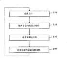
接着,对使用上述成膜装置100的实施例1的成膜方法进行说明。图2A是表示本发明的实施例1的基板处理方法的概要的流程图。参照图2A,首先,在步骤10(图中以S10表示,以下相同)中,从上述气体管线120和/或上述气体管线130向由上述处理容器101、102构成的上述内部空间101A供给原料气体,在被处理基板上进行成膜(例如进行W膜的成膜)。Next, the film forming method of Example 1 using the
此外,并不限于对一个被处理基板进行成膜处理,也可以连续对多个被处理基板进行成膜。In addition, the film formation process is not limited to one substrate to be processed, and film formation may be continuously performed on a plurality of substrates to be processed.
接着,在步骤20中,向上述内部空间101A供给已进行等离子体激励的清洁气体(例如NF3等氟化合物气体),对堆积在处理容器内的堆积物进行清洁。以该情况下,现有技术中主要使用由上述远程等离子体产生装置141生成的清洁气体的自由基,对堆积物进行蚀刻。Next, in
但是,在本实施例的清洁中,因为使处理容器内(上述内部空间101A)的压力为规定压力以上,所以在上述内部空间101A中,利用自由基再结合而成的分子对堆积物进行的蚀刻起支配作用。However, in the cleaning of this embodiment, since the pressure in the processing container (the above-mentioned
因此,清洁的对象膜(例如W膜)的蚀刻速率被维持在较高水平,并且能够抑制对处理容器内的部件(例如构成上述保持台盖105的石英等)造成的损伤。对于这些压力和蚀刻速率在以后进行详细说明。Therefore, the etching rate of the film to be cleaned (for example, the W film) is maintained at a high level, and damage to components in the processing container (for example, quartz constituting the above-mentioned holding table cover 105 ) can be suppressed. These pressures and etching rates will be described in detail later.
接着,在步骤30中,从上述气体管线120和/或上述气体管线130供给例如Ar等惰性气体,从而对上述内部空间101A进行吹扫。本步骤也能够省略,但是,通过设置本步骤的处理,能够抑制处理容器内颗粒的产生。Next, in
接着,在清洁后,为了抑制例如Al的氟化物(AlF)等污染、颗粒的产生源向处理容器内扩散,对上述内部空间101A内的上述例如处理容器101的内壁、上述保持台104等进行涂膜(coating film)的成膜。该涂膜只要形成为与例如步骤10中在被处理基板上形成的膜相同的膜即可。Next, after cleaning, in order to prevent contamination such as Al fluoride (AlF) and the like from spreading into the processing container, the inner wall of the
在现有技术中,即使在形成有这种涂膜的情况下,根据涂膜的成膜条件的不同,Al的氟化物可能会在处理容器内扩散,难以利用涂膜抑制颗粒、污染的产生。In the prior art, even when such a coating film is formed, Al fluoride may diffuse in the processing container depending on the film-forming conditions of the coating film, and it is difficult to suppress the generation of particles and contamination by the coating film .
例如,在进行涂膜的成膜时,如果上述保持台104为与通常的成膜处理时相同的高温(在包括W膜等的金属的CVD法的情况下,例如为500℃~600℃左右),会产生在形成涂膜之前,AlF(主要从上述保持台104)向上述内部空间101A蒸发扩散的问题。For example, when forming a coating film, if the above-mentioned holding table 104 is at the same high temperature as the normal film forming process (in the case of a metal CVD method including a W film, for example, about 500° C. to 600° C. ), there will be a problem that AlF (mainly from the above-mentioned holding table 104) evaporates and diffuses into the above-mentioned
因此,在本实施例中,使涂膜的成膜时的保持台的温度比先前说明的步骤10的通常的成膜处理时的温度低。由此,在AlF的蒸气压较低的状态下对保持台表面、处理容器等进行涂敷。结果,能够抑制AlF的产生,抑制颗粒、污染的产生。这些涂膜形成时的保持台104的温度与AlF的产生的关系在后面进行叙述。Therefore, in the present embodiment, the temperature of the holding table during the film formation of the coating film is lower than the temperature during the normal film formation process in
此外,这样在低温下进行涂膜的成膜从而抑制AlF的产生的效果,通过与对处理容器内的部件的损伤小、步骤20的在高压力下进行的清洁相组合,能够更为显著。即,在现有技术的主要使用自由基的清洁中,不仅会对处理容器内的石英等部件造成损伤,而且虽然蚀刻量较小,但也会对AlN、Al2O3等构成保持台的材料造成损伤。因此,进行能够抑制对AlN、Al2O3等的损伤(与F反应)的、以分子为主体的蚀刻(清洁),并进一步通过在低温下形成涂膜,能够使抑制AlF扩散的效果更加显著。In addition, the effect of suppressing the generation of AlF by forming a coating film at a low temperature in this way can be more remarkable in combination with the cleaning under high pressure in
在上述涂敷成膜之后,上述内部空间101A保持洁净,能够再次实施成膜,能够使处理返回到步骤10。After the above coating and film formation, the
这样,在本实施例的基板处理方法中,作为清洁对象的堆积物的蚀刻速率变高,另一方面,能够抑制处理容器、处理容器内的部件的损伤,并进一步抑制AlF等的产生。因此,能够高效地保持成膜装置的处理容器内的清洁,使生产率良好。In this way, in the substrate processing method of this embodiment, the etching rate of the deposit to be cleaned is increased, and damage to the processing chamber and parts in the processing chamber can be suppressed, and generation of AlF and the like can be further suppressed. Therefore, it is possible to efficiently keep the inside of the processing container of the film forming apparatus clean and improve productivity.
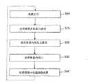
此外,上述图2A所示的基板处理方法也可以变更为图2B所示的方法。其中,对图中已经说明的部分标注相同的参照符号并省略说明。In addition, the substrate processing method shown in FIG. 2A may be changed to the method shown in FIG. 2B . However, the same reference numerals are assigned to the parts already explained in the drawings, and description thereof will be omitted.
参照图2B,在本图所示的方法中,在步骤10和步骤20之间追加有步骤15的处理。在步骤15中,上述内部空间101A的压力比步骤20的情况下的上述内部空间101A的压力低,以尽可能不消减已进行等离子体激励的清洁气体的自由基的方式进行使用自由基的清洁。Referring to FIG. 2B , in the method shown in this figure, the processing of
该方法是,例如在上述内部空间101A中,在结构上存在有温度不能上升的位置,例如处理容器的角落等的情况下,用于使清洁对象(例如W膜)和处理容器内的部件(例如SiO2)的蚀刻的选择比良好的方法。这些内容将在后面进行详细说明。This method is, for example, in the above-mentioned
此外,上述图2B所示的基板处理方法也可以变更为图2C所示的方法。其中,对图中已经说明的部分标注相同的参照符号并省略说明。In addition, the substrate processing method shown in FIG. 2B may be changed to the method shown in FIG. 2C . However, the same reference numerals are assigned to the parts already explained in the drawings, and description thereof will be omitted.
参照图2C,在本图所示的方法中,在步骤40之后追加有步骤45。与步骤40的上述保持台104的温度相比,使步骤45中的上述保持台104的温度升高,并进行涂敷成膜。通过设置本步骤,能够形成膜质更加良好的涂膜,能够达到使涂膜的密接性良好的效果。Referring to FIG. 2C , in the method shown in this figure, step 45 is added after
接着,下面基于使用上述成膜装置100进行的实验结果,对上述所示的基板处理方法的效果进行说明。以下表示的数据和图表是本发明的发明人使用上述成膜装置100得到的结果。Next, the effects of the above-described substrate processing method will be described below based on the results of experiments performed using the above-described
图3是表示使用通过上述远程等离子体产生装置141进行等离子体激励的清洁气体,在上述成膜装置100的上述内部空间101A(上述保持台104上)进行的蚀刻速率的测定结果的图。在图3中,分别表示在使上述内部空间101A的压力变化的情况下的W膜的蚀刻速率(图中以◆表示W)和热氧化膜的蚀刻速率(图中以■表示T-Ox)。在该情况下,清洁气体(NF3)的流量为210sccm,稀释气体(Ar)的流量为3000sccm,保持台的温度为500℃。3 is a graph showing the measurement results of the etching rate in the
参照图3,随着上述内部空间101A的压力增大,热氧化膜的蚀刻速率迅速降低。另一方面,W膜的蚀刻速率随着上述内部空间101A的压力的上升而缓慢上升。Referring to FIG. 3, as the pressure of the above-mentioned
这被认为是因为随着上述内部空间101A的压力的增大,NF3进行等离子体激励而生成的F自由基消减并再结合,生成F分子(F2),主要是F分子的蚀刻起支配作用。因此,认为尤其是热氧化膜的蚀刻速率迅速降低。This is considered to be because as the pressure of the
在该情况下,考虑到热氧化膜的蚀刻量与构成上述保持台盖105的石英材料(SiO2)的蚀刻量之间相互关联,可知通过增大上述内部空间101A的压力能够抑制石英材料的损伤量(蚀刻量)。此外,同样的,认为也能够降低构成保持台的AlN或Al2O3的损伤量。In this case, considering the correlation between the etching amount of the thermally oxidized film and the etching amount of the quartz material (SiO2 ) constituting the above-mentioned
另一方面,W膜的蚀刻速率随着上述内部空间101A的压力的增大而变大。On the other hand, the etching rate of the W film becomes larger as the pressure of the above-mentioned
图4表示的是在上述情况下,上述内部空间101A的压力与W膜的蚀刻的活化能的关系。参照图4可知,该活化能在上述内部空间101A的压力为20Torr(2666Pa)以上的区域中尤为迅速地增大。即,可知上述内部空间101A的压力优选为20Torr(2666Pa)以上。在该情况下,能够在较高地维持堆积在处理容器内的堆积物(W膜)的蚀刻速率的同时,抑制处理容器内的部件(石英等)的损伤。FIG. 4 shows the relationship between the pressure of the
此外,图5是表示在上述实验中,变更上述保持台104的温度(250℃、350℃、500℃)的情况下的上述内部空间101A的压力与热氧化膜和W膜的蚀刻速率的比的关系的图。在该情况下,蚀刻速率的比是W膜的蚀刻速率相对热氧化膜的蚀刻速率的比(W膜的蚀刻速率/热氧化膜的蚀刻速率,下文中称为蚀刻速率比)。图中,■表示保持台的温度为250℃时的结果,口表示保持台的温度为350℃时的结果,△表示保持台的温度为500℃时的结果。5 shows the ratio of the pressure in the
参照图5可知,在上述保持台104的温度为350℃和500℃的情况下,随着上述内部空间101A的压力的增大,上述蚀刻速率比增大,能够在抑制处理容器内的部件的损伤的同时高效地对清洁的对象膜进行蚀刻。Referring to FIG. 5, it can be seen that when the temperature of the above-mentioned holding table 104 is 350° C. and 500° C., as the pressure of the above-mentioned
另一方面,在上述保持台104的温度为250℃的情况下,相反的,随着上述内部空间101A的压力的增大,蚀刻速率比有稍微减小的倾向。因此,在使上述内部空间101A的压力为20Torr以上并进行高压力清洁的情况下,优选上述保持台104的温度为350℃以上。即,在上述图2A所示的步骤20中,优选上述内部空间101A的压力为20Torr(2666Pa)以上,在该情况下优选上述保持台104的温度为350度以上。On the other hand, when the temperature of the holding table 104 is 250° C., on the contrary, the etching rate ratio tends to slightly decrease as the pressure of the
图6是表示在上述图5所示的情况下,设置在上述内部空间101A中的部件(例如上述保持台盖105)的更换周期的图。其中,对图中先前已说明的部分标注相同的参照符号并省略说明。此外,在本图中省略上述保持台104的温度为250℃的情况的记载。FIG. 6 is a diagram showing replacement cycles of components (for example, the holding table cover 105 ) installed in the
如上所述,因为上述保持台盖105利用厚度实现其功能,所以如果变薄10%左右则有必要进行更换。在图6中记载有根据蚀刻速率计算出的在月产1000个的处理的情况下,其更换的周期。As described above, since the holding
参照图6,在上述保持台104的温度为350℃和500℃的情况下显示大致相同的结果,在上述内部空间101A的压力为15Torr(2000Pa)以上时,更换周期为3个月以上,在该压力为30Torr(4000Pa)以上时,更换周期约为12个月以上。于是可知,通过增大上述内部空间101A的压力并进行清洁,能够降低该内部空间101A的部件的损伤,能够延长部件的更换周期,进行生产率高的基板处理。Referring to FIG. 6 , substantially the same results are shown when the temperature of the above-mentioned holding table 104 is 350° C. and 500° C. When the pressure of the above-mentioned
另一方面,如图5所示,在上述保持台104的温度为250℃的情况下,相反的,随着上述内部空间101A的压力的增大,蚀刻速率比有减少的倾向,而低压侧的蚀刻速率比变得较高。On the other hand, as shown in FIG. 5, when the temperature of the above-mentioned holding table 104 is 250°C, on the contrary, as the pressure of the above-mentioned
因此,在上述内部空间101A中存在温度难以上升的位置的情况下,或者在上述内部空间101A中产生温度不均,存在部分温度较低的状态(以下称为低温位置)的情况下,为了蚀刻该低温位置的堆积物,优选使上述内部空间101A的压力较低。在该情况下,为了也能够在上述保持台104侧防止对部件的损伤,优选使温度降低。Therefore, in the case where there is a position where the temperature is difficult to rise in the
即,在对包括该低温位置的处理容器内进行清洁的情况下,优选设置步骤,如先前在图2B中说明的基板处理方法的上述步骤15那样,使上述内部空间101A的压力比上述步骤20的情况下的压力低,并使上述保持台104的温度比上述步骤20的情况下的温度低,进行上述低温位置的清洁。That is, in the case of cleaning the inside of the processing container including this low-temperature position, it is preferable to provide a step of making the pressure of the
此外,在该步骤15中,根据图5所示的结果,上述内部空间101A的压力为10Torr(1330Pa)以下,更优选为5Torr(665Pa)以下,优选上述保持台104的温度为300℃以下。In addition, in this
此外,在图7和图8中分别表示在变更上述内部空间101A的压力和上述保持台104的温度的情况下,W膜的蚀刻速率(图7)和热氧化膜的蚀刻速率(图8)。在图中,横轴表示上述保持台104的温度,纵轴表示蚀刻速率。In addition, FIG. 7 and FIG. 8 respectively show the etching rate of the W film ( FIG. 7 ) and the etching rate of the thermal oxide film ( FIG. 8 ) when the pressure of the
此外,在图7和图8中,◆表示上述内部空间101A的压力为1Torr(133Pa)、NF3的流量为210sccm的情况(图中记作◆1T 210),以下同样的,口表示上述内部空间101A的压力为40Torr(5332Pa)、NF3的流量为210sccm的情况(图中记作口40T 210),▲表示上述内部空间101A的压力为1Torr、NF3的流量为310sccm的情况(图中记作▲1T 310),○表示上述内部空间101A的压力为20Torr(2666Pa)、NF3的流量为280sccm的情况(图中记作○20T 280)。In addition, in FIG. 7 and FIG. 8, ◆ represents the case where the pressure of the above-mentioned
首先,参照图7可知,在蚀刻W膜时,在上述内部空间101A的压力较高(20Pa以上)的情况下,上述保持台104的温度增大时,蚀刻量增大。另一方面,在上述内部空间101A的压力较低(1Torr以下)的情况下,蚀刻速率由压力引起的变化较小。此外,在保持台为低温(250℃以下)时,在压力较高的情况下(20Pa以上)蚀刻速率极度变小,在压力较低的情况下(1Torr以下)蚀刻速率较高,倾向是反转的。First, referring to FIG. 7 , when the W film is etched, when the pressure of the
另一方面,参照图8可知,在蚀刻热氧化膜时,虽然整体上压力较低的一方蚀刻速率较大,但是在压力较低(1Torr以下)的情况下,随着温度的降低,蚀刻速率有迅速下降的倾向。因此,上述蚀刻速率比如图5中已说明的那样,在保持台的温度为250℃时,低压力(1Torr以下)的一方蚀刻速率比较高,产生与保持台的温度为高温的情况相反的现象。On the other hand, referring to FIG. 8, it can be seen that when etching a thermal oxide film, although the overall etching rate is higher at a lower pressure, when the pressure is lower (below 1 Torr), the etching rate decreases as the temperature decreases. have a tendency to decline rapidly. Therefore, the above-mentioned etching rate is as described in FIG. 5. When the temperature of the holding table is 250° C., the etching rate is relatively high at a low pressure (1 Torr or less), and the opposite phenomenon occurs when the temperature of the holding table is at a high temperature. .
鉴于上述观点,为了使上述蚀刻速率比变高,优选升高上述保持台104的温度(例如上述已经说明的350℃以上),使上述内部空间101A的压力变高(例如上述已经说明的20Torr以上,进一步优选为30Torr以上)。但是,另一方面,当存在蚀刻对象膜的温度较低(250℃以下)的位置的情况下,优选使上述内部空间101A的压力降低(1Torr以下)。在该情况下,为了降低对该保持台104、上述保持台盖105的损伤,上述保持台104的温度优选为250℃以下。这些低温、低压的清洁与图2B所示的步骤15的处理相对应。In view of the above viewpoint, in order to increase the above-mentioned etching rate ratio, it is preferable to increase the temperature of the above-mentioned holding table 104 (for example, 350° C. or higher as described above), and to increase the pressure of the
接着,对图2A~图2C的步骤40的该涂敷处理的抑制污染的效果进行说明。Next, the contamination suppression effect of the coating process in
如上述说明的那样,在清洁后,通过对上述处理容器101、102的内壁而、上述保持台104、上述保持台盖105、上述喷淋头部109(与内部空间101A相对的对象)等进行涂敷成膜,能够抑制例如AlF的扩散,防止颗粒、污染的扩散。As described above, after cleaning, cleaning is performed on the inner walls of the
但是,在现有技术中进行这样的涂敷成膜时,在清洁气体中使用含有F的气体时,其与处理容器、处理容器内的Al反应,生成AlF,由于AlF的扩散而成为颗粒、污染的产生原因。However, when performing such coating and film formation in the prior art, when a gas containing F is used as the cleaning gas, it reacts with the processing container and Al in the processing container to generate AlF, which becomes particles, The cause of pollution.
因此,在本实施例中,抑制涂敷成膜时的上述保持台104的温度,使其比通常在被处理基板上进行成膜时的温度低,抑制AlF的扩散并实施涂敷成膜,之后,使保持台升温至通常进行成膜所必需的温度。Therefore, in this embodiment, the temperature of the above-mentioned holding table 104 during coating and film formation is suppressed to be lower than the temperature when a film is usually formed on a substrate to be processed, and the diffusion of AlF is suppressed to perform coating and film formation. Thereafter, the temperature of the holding table is raised to a temperature generally required for film formation.
例如,在利用CVD法(MOCVD法)形成金属膜、金属氮化膜(也包括添加有Si的情况)等的情况下,上述保持台104(被处理基板)的温度优选为500℃~600℃,或者这以上的温度。作为这样的例子,列举使用W(CO)6、SiH4、NH3作为原料形成W膜、WN膜、WSi膜、SiN膜的情况,或者使用Ta(Nt-Am)(NMe2)3、NH3、SiH4作为原料形成TaSiN膜的情况等。For example, when forming a metal film, a metal nitride film (including the case where Si is added) or the like by CVD (MOCVD), the temperature of the holding table 104 (substrate to be processed) is preferably 500°C to 600°C. , or temperatures above this. Examples of this include the case where W(CO)6 , SiH4 , and NH3 are used as raw materials to form a W film, WN film, WSi film, and SiN film, or Ta(Nt-Am)(NMe2 )3 , NH 33. The case where SiH4 is used as a raw material to form a TaSiN film, etc.
在现有技术中,在进行涂敷成膜时,不改变通常的向被处理基板进行成膜时的任何条件。因此,在清洁中形成的Al的氟化物,例如因上述保持台104的温度增大而升华并扩散,成为成膜时的污染的原因,此外产生在处理容器内凝固,成为颗粒产生的原因的情况。In the prior art, when forming a film by coating, the general conditions for forming a film on a substrate to be processed are not changed at all. Therefore, the Al fluoride formed during cleaning, for example, sublimates and diffuses due to an increase in the temperature of the above-mentioned holding table 104, causing contamination during film formation, and solidifies in the processing container to cause particle generation. Condition.
因此,在本实施例中,例如在图2A~图2C所示的步骤40中,使上述保持台104的温度比步骤10的情况下的温度低,并进行涂敷成膜,在AlF扩散之前以低温形成涂膜,从而抑制污染、颗粒的产生。Therefore, in this embodiment, for example, in
接着,说明对涂敷成膜时的保持台104的温度与其后的成膜工序中形成的膜的污染的关系进行调查的结果。图9表示在涂敷成膜时上述保持台104的温度为400℃和450℃的情况下,在涂敷成膜后,分别对在被处理基板上成膜的膜的杂质进行调查的结果。对保持台的温度为400℃的情况下的三个被处理基板(晶片)、保持台的温度为450℃的情况下的两个被处理基板,调查所形成的膜。图中左端的编号表示任意的晶片ID编号。此外,各元素的检测结果的单位为1010atoms/cm3。Next, the results of investigation of the relationship between the temperature of the holding table 104 during coating film formation and the contamination of the film formed in the subsequent film formation process will be described. 9 shows the results of investigations of impurities in films formed on the substrate to be processed after coating and film formation when the temperature of the holding table 104 was 400°C and 450°C during coating and film formation. Films formed on three substrates (wafers) to be processed when the temperature of the holding table was 400°C and two substrates to be processed when the temperature of the holding table was 450°C were examined. The numbers at the left end in the figure represent arbitrary wafer ID numbers. In addition, the unit of the detection result of each element is 1010 atoms/cm3 .
参照图9,在保持台的温度为450℃的情况下,与保持台的温度为400℃的情况相比,尤其是Al的污染量变大,如已经说明的那样,认为原因是保持台的温度上升引起的AlF的扩散。此外,还检测出Cr、Fe等重金属。这被认为是因为例如处理容器、保持台中所含有的重金属的析出。因此,上述步骤40中的上述保持台104的温度(涂敷成膜时的保持台的温度)优选为430℃以下,使得Al污染量在作为允许值的5×10¹⁰atoms/cm3以下,当为400℃以下时能够进一步减少污染物质的含有量,因此更加优选。Referring to Fig. 9, when the temperature of the holding table is 450°C, the amount of Al contamination in particular becomes larger than when the temperature of the holding table is 400°C. As already explained, the cause is considered to be the temperature of the holding table. rise caused by the diffusion of AlF. In addition, heavy metals such as Cr and Fe were also detected. This is considered to be due to, for example, precipitation of heavy metals contained in the processing container and the holding stand. Therefore, the temperature of the above-mentioned holding table 104 in the above-mentioned step 40 (the temperature of the holding table during coating and film formation) is preferably 430° C. or lower, so that the amount of Al contamination is below the allowable value of 5×10¹⁰ atoms/cm3 , When it is 400° C. or lower, the content of pollutants can be further reduced, so it is more preferable.
图10以一个图总括地表示温度和AlF的蒸气压的关系,以及涂敷成膜时的上述保持台104的温度和涂敷成膜后在被处理基板上成膜的膜的Al杂质的检测结果的关系。在该情况下,作为图的纵轴的AlF的蒸气压表示为以400℃的AlF的蒸气压为1时的AlF的蒸气压的比。此外,Al的检测结果中以●表示平均值,以I表示最小值和最大值的间隔。FIG. 10 shows in one graph the relationship between temperature and the vapor pressure of AlF, and the temperature of the above-mentioned holding table 104 during coating and film formation, and the detection of Al impurities in the film formed on the substrate to be processed after coating and film formation. result relationship. In this case, the vapor pressure of AlF on the vertical axis of the graph represents the ratio of the vapor pressure of AlF when the vapor pressure of AlF at 400° C. is 1. In addition, in the detection results of Al, ● represents the average value, and I represents the interval between the minimum value and the maximum value.
参照图10,AlF的蒸气压在400℃时为450℃时的大致100分之1,与此相对应,Al污染量也成为大致100分之1左右。即,能够确认AlF的蒸气压的减少和成膜时的Al污染量的相关关系,因此可知,通过在涂敷成膜时使保持台为低温,能够抑制Al的污染量。Referring to FIG. 10 , the vapor pressure of AlF at 400° C. is approximately 1/100 of that at 450° C., and accordingly, the amount of Al contamination is also approximately 1/100. That is, since the correlation between the reduction of the vapor pressure of AlF and the amount of Al contamination during film formation was confirmed, it was found that the amount of Al contamination can be suppressed by keeping the holding table at a low temperature during coating and film formation.
接着,对在图2A~图2C中已经说明的、上述步骤30的对处理容器内的吹扫的减少颗粒的效果进行说明。步骤30所示的对上述内部空间101A的吹扫是指,反复进行向上述内部空间101A供给例如Ar等惰性气体和从该内部空间101A排出该惰性气体的处理,将微粒、污染物质等向该内部空间101A之外排出的处理。Next, the particle reduction effect of purging the inside of the processing container in
图11表示在图2A所示的基板处理方法中,在实施与不实施步骤30(吹扫)的情况下,各自的被处理基板的表面的微粒的密度(/m2)。图中,■表示不实施吹扫的情况下的0.2μm以上的颗粒的密度,口表示不实施吹扫的情况下的0.1μm以上的颗粒的密度,●表示实施吹扫的情况下的0.2μm以上的颗粒的密度,○表示实施吹扫的情况下的0.1μm以上的颗粒的密度。FIG. 11 shows the particle density (/m2 ) on the surface of the substrate to be processed in the substrate processing method shown in FIG. 2A , with and without step 30 (purging). In the figure, ■ indicates the density of particles larger than 0.2 μm without purging, 口 indicates the density of particles larger than 0.1 μm in the case of not purging, ● indicates the density of particles of 0.2 μm in the case of purging For the density of the particles above, ◯ represents the density of particles of 0.1 μm or more when purging is performed.
此外,图12表示在图2A所示的基板处理方法中,在实施与不实施步骤30(吹扫)的情况下,各自的被处理基板的背面的微粒的密度(/m2)。图中,■表示不实施吹扫的情况下的0.12μm以上的颗粒的密度,●表示实施吹扫的情况下的0.12μm以上的颗粒的密度。In addition, FIG. 12 shows the particle density (/m2 ) on the back surface of each substrate to be processed under the conditions of implementing and not implementing step 30 (purge) in the substrate processing method shown in FIG. 2A . In the figure, ■ represents the density of particles with a diameter of 0.12 μm or more when no purging is performed, and ● represents the density of particles with a diameter of 0.12 μm or greater when purging is performed.
参照图11、图12能够确认,在进行吹扫处理的情况下,被处理基板的表面和背面的颗粒的密度均减少,通过进行吹扫处理,能够达到减少颗粒的效果。Referring to FIG. 11 and FIG. 12 , it can be confirmed that when the purge treatment is performed, the particle densities on both the surface and the back surface of the substrate to be processed are reduced, and the effect of particle reduction can be achieved by performing the purge treatment.
实施例2Example 2
接着,基于上述基板处理方法,对使用上述成膜装置100实施基板处理方法的例子进行说明。在以下的例子中,基于图2A所示的基板处理方法进行基板处理。Next, based on the substrate processing method described above, an example in which the substrate processing method is implemented using the
首先,如下上述进行步骤10的处理。使上述保持台104的温度为672℃,使用例如搬送机械手等将被处理基板(300mm晶片)搬入上述内部空间101A。First, the processing of
接着,使保持在上述原料供给装置130C中的W(CO)6升华成为原料气体,与作为载气的Ar90sccm和作为稀释气体(吹扫气体)的Ar700sccm一起,通过上述气体管线130从上述喷淋头部109供给上述内部空间101A。在该情况下,上述内部空间101A的压力为20Pa(0.15Torr)。结果,原料气体在被处理基板上分解,在被处理基板上形成W膜。成膜时间为150秒,形成厚度约为20nm的W膜。对250个被处理基板实施该处理。Next, the W(CO)6 held in the raw
接着,以下述方式实施步骤20的处理。首先使上述保持台104的温度下降至400℃。接着向上述远程等离子体产生装置141供给230sccm的NF3、3000sccm的Ar,并施加2.7kW的高频电力进行等离子体激励,生成含有F自由基的活性种。Next, the process of
由上述远程等离子体产生装置141进行等离子体激励的清洁气体(包括稀释气体)通过上述气体管线140从上述喷淋头部109供给上述内部空间101A。在该情况下,上述内部空间101A的压力为5320Pa(39.9Torr)。该清洁处理实施30分钟。The cleaning gas (including diluent gas) plasma-excited by the
接着,为了确认清洁,打开上述处理容器101,确认处理容器内部的状态,确认已除去堆积在处理容器内壁、喷淋头部、保持台、保持台盖等上的W膜,并且没有对这些部件造成损伤。Next, in order to confirm the cleanliness, the above-mentioned
此外,之后实施步骤30、步骤40,进而使处理返回步骤10,由此能够连续地进行基板处理。In addition,
例如,在步骤30中,反复进行向上述内部空间101A供给例如Ar等惰性气体,和从该内部空间101A排出该惰性气体的处理,即实施循环吹扫即可。For example, in
此外,在步骤40中,除保持台的温度以外与步骤10的成膜工序为相同的条件,将上述保持台104的温度变更为例如400℃,并进行涂敷成膜即可。In addition, in
实施例3Example 3
接着,基于图2B所示的基板处理方法,对进行基板处理的例子进行说明。Next, an example of performing substrate processing based on the substrate processing method shown in FIG. 2B will be described.
首先,如下所述进行步骤10的处理。使上述保持台104的温度为600℃,使用例如搬送机械手等将被处理基板(300mm晶片)搬入上述内部空间101A。First, the processing of
接着,使在上述原料供给装置中保持在46℃的Ta(Nt-Am)(NMe2)3升华成为原料气体,与作为载气的Ar40sccm一起通过上述气体管线130从上述喷淋头部109供给上述内部空间101A。在该情况下,同样的,将作为稀释气体(吹扫气体)的40sccm的Ar、500sccm的SiH4、200sccm的NH3同时通过上述气体管线120从上述喷淋头部109供给上述内部空间101A。Next, Ta(Nt-Am)(NMe2 )3 kept at 46°C in the above-mentioned raw material supply device was sublimated into a raw material gas, and supplied from the
在该情况下,上述内部空间101A的压力为40Pa(0.3Torr)。结果,原料气体在被处理基板上分解,在被处理基板上形成TaSiN膜。成膜时间为150秒,形成厚度约为20nm的TaSiN膜。对250个被处理基板实施该处理。In this case, the pressure of the
接着,如下所述实施步骤15的处理。首先使上述保持台104的温度下降至250℃。接着向上述远程等离子体产生装置141供给230sccm的NF3、3000sccm的Ar,并施加1.2kW的高频电力进行等离子体激励,生成含有F自由基的活性种。Next, the processing of
由上述远程等离子体产生装置141进行等离子体激励的清洁气体(包括稀释气体)通过上述气体管线140从上述喷淋头部109供给上述内部空间101A。在该情况下,上述内部空间101A的压力为133Pa(1Torr)。该清洁处理实施10分钟。The cleaning gas (including diluent gas) plasma-excited by the
接着,如下所述实施步骤20的处理。首先使上述保持台104的温度上升至400℃。接着向上述远程等离子体产生装置141供给230sccm的NF3、3000sccm的Ar,并施加2.7kW的高频电力进行等离子体激励,生成含有F自由基的活性种。Next, the processing of
由上述远程等离子体产生装置141进行等离子体激励的清洁气体(包括稀释气体)通过上述气体管线140从上述喷淋头部109供给上述内部空间101A。在该情况下,上述内部空间101A的压力为5320Pa(39.9Torr)。该清洁处理实施30分钟。The cleaning gas (including diluent gas) plasma-excited by the
接着,作为步骤30的处理,使用Ar作为吹扫气体,反复进行Ar的供给和供给的停止,即实施所谓的循环吹扫。即,实施反复使ArlTorr(133Pa)1000sccm或Ar0.5Torr(66.5Pa)800sccm保持20sec、其后抽真空10sec的循环吹扫。Next, as the process of
接着,作为步骤40,除保持台的温度以外与该步骤10的成膜工序为相同的条件,将上述保持台104的温度变更为例如400℃,并进行涂敷成膜。Next, as
之后,使处理再次返回步骤10并进行成膜,确认微粒和膜中的Al的污染减少。Thereafter, the process was returned to step 10 again to form a film, and it was confirmed that contamination of fine particles and Al in the film was reduced.
此外,在实施图2C所示的基板处理方法时,在该步骤40中以400℃进行涂敷成膜后,与步骤45的处理相对应,将保持台的温度变更为例如与步骤10相同的600℃,并同样实施涂敷成膜即可。在该情况下,涂膜的膜质良好,涂膜的密接性良好。In addition, when implementing the substrate processing method shown in FIG. 2C , after coating and film formation at 400° C. in this
此外,上述实施例对在被处理基板上形成含有W、Ta的膜的情况进行了说明,但是本发明并不局限于此,能够使用金属羰基气体(metalcarbonyl gas)等各种原料气体进行各种成膜。此外,以使用NF3作为清洁气体的情况为例进行了说明,但是并不限定与此,例如能够使用氟烃(fluorocarbon)类等具有F的各种清洁气体。In addition, the above-mentioned examples have described the case where a film containing W and Ta is formed on the substrate to be processed, but the present invention is not limited thereto, and various raw material gases such as metal carbonyl gas can be used for various processes. film forming. In addition, the case of using NF3 as the cleaning gas has been described as an example, but it is not limited to this, and various cleaning gases having F such as fluorocarbons can be used, for example.
产业上的可利用性Industrial availability
根据本发明,能够提供高效地保持成膜装置的处理容器内的清洁并且生产率良好的基板处理方法,和存储有在计算机中运行该基板处理方法的程序的记录介质。According to the present invention, it is possible to provide a substrate processing method that efficiently keeps the inside of a processing container of a film forming apparatus clean and has good productivity, and a recording medium storing a program for executing the substrate processing method on a computer.
本国际申请主张基于2005年9月26日提出申请的日本专利申请2005-278367号的优选权,在本国际申请中引用2005-278367号的全部内容。This international application claims priority based on Japanese Patent Application No. 2005-278367 filed on September 26, 2005, and the entire content of Japanese Patent Application No. 2005-278367 is cited in this international application.
Claims (14)
Applications Claiming Priority (2)
| Application Number | Priority Date | Filing Date | Title |
|---|---|---|---|
| JP2005278367AJP4823628B2 (en) | 2005-09-26 | 2005-09-26 | Substrate processing method and recording medium |
| JP278367/2005 | 2005-09-26 |
Publications (1)
| Publication Number | Publication Date |
|---|---|
| CN101273154Atrue CN101273154A (en) | 2008-09-24 |
Family
ID=37888679
Family Applications (1)
| Application Number | Title | Priority Date | Filing Date |
|---|---|---|---|
| CNA2006800354936APendingCN101273154A (en) | 2005-09-26 | 2006-07-25 | Substrate processing method and recording medium |
Country Status (5)
| Country | Link |
|---|---|
| US (1) | US20090117270A1 (en) |
| JP (1) | JP4823628B2 (en) |
| KR (1) | KR101012959B1 (en) |
| CN (1) | CN101273154A (en) |
| WO (1) | WO2007034624A1 (en) |
Cited By (4)
| Publication number | Priority date | Publication date | Assignee | Title |
|---|---|---|---|---|
| CN111101114A (en)* | 2018-10-29 | 2020-05-05 | 三星电子株式会社 | Cleaning method of film deposition chamber |
| CN112166491A (en)* | 2018-06-15 | 2021-01-01 | 应用材料公司 | Techniques for implementing high temperature cleaning for rapid wafer processing |
| CN113161224A (en)* | 2020-01-23 | 2021-07-23 | 东京毅力科创株式会社 | Film forming method and film forming apparatus |
| CN114530404A (en)* | 2020-11-05 | 2022-05-24 | 东京毅力科创株式会社 | Substrate holder, substrate transfer device, and method for manufacturing substrate holder |
Families Citing this family (93)
| Publication number | Priority date | Publication date | Assignee | Title |
|---|---|---|---|---|
| JP4885025B2 (en)* | 2007-03-26 | 2012-02-29 | 三菱重工業株式会社 | Vacuum processing apparatus and operating method of vacuum processing apparatus |
| WO2009034610A1 (en)* | 2007-09-11 | 2009-03-19 | Canon Anelva Corporation | Method of preventing detachment of deposited film on substrate retention tool in thin-film forming apparatus and thin-film forming apparatus |
| EP2290124A1 (en) | 2008-06-27 | 2011-03-02 | Mitsubishi Heavy Industries, Ltd. | Vacuum processing apparatus and method for operating vacuum processing apparatus |
| US10283321B2 (en) | 2011-01-18 | 2019-05-07 | Applied Materials, Inc. | Semiconductor processing system and methods using capacitively coupled plasma |
| JP6101113B2 (en) | 2012-03-30 | 2017-03-22 | 株式会社日立国際電気 | Semiconductor device manufacturing method, cleaning method, substrate processing apparatus, and program |
| JP5729351B2 (en)* | 2012-05-18 | 2015-06-03 | 信越半導体株式会社 | Semiconductor wafer cleaning method |
| US9373517B2 (en) | 2012-08-02 | 2016-06-21 | Applied Materials, Inc. | Semiconductor processing with DC assisted RF power for improved control |
| US9132436B2 (en) | 2012-09-21 | 2015-09-15 | Applied Materials, Inc. | Chemical control features in wafer process equipment |
| US10256079B2 (en) | 2013-02-08 | 2019-04-09 | Applied Materials, Inc. | Semiconductor processing systems having multiple plasma configurations |
| JP6063293B2 (en)* | 2013-02-22 | 2017-01-18 | 大陽日酸株式会社 | Vapor growth method |
| US9362130B2 (en) | 2013-03-01 | 2016-06-07 | Applied Materials, Inc. | Enhanced etching processes using remote plasma sources |
| JP2015183260A (en)* | 2014-03-25 | 2015-10-22 | 株式会社日立国際電気 | Cleaning method, substrate processing apparatus, and program |
| US9309598B2 (en) | 2014-05-28 | 2016-04-12 | Applied Materials, Inc. | Oxide and metal removal |
| US9368364B2 (en)* | 2014-09-24 | 2016-06-14 | Applied Materials, Inc. | Silicon etch process with tunable selectivity to SiO2 and other materials |
| US9355922B2 (en) | 2014-10-14 | 2016-05-31 | Applied Materials, Inc. | Systems and methods for internal surface conditioning in plasma processing equipment |
| US9966240B2 (en) | 2014-10-14 | 2018-05-08 | Applied Materials, Inc. | Systems and methods for internal surface conditioning assessment in plasma processing equipment |
| US11637002B2 (en) | 2014-11-26 | 2023-04-25 | Applied Materials, Inc. | Methods and systems to enhance process uniformity |
| US10224210B2 (en) | 2014-12-09 | 2019-03-05 | Applied Materials, Inc. | Plasma processing system with direct outlet toroidal plasma source |
| US10573496B2 (en) | 2014-12-09 | 2020-02-25 | Applied Materials, Inc. | Direct outlet toroidal plasma source |
| US11257693B2 (en) | 2015-01-09 | 2022-02-22 | Applied Materials, Inc. | Methods and systems to improve pedestal temperature control |
| US20160225652A1 (en) | 2015-02-03 | 2016-08-04 | Applied Materials, Inc. | Low temperature chuck for plasma processing systems |
| US9728437B2 (en) | 2015-02-03 | 2017-08-08 | Applied Materials, Inc. | High temperature chuck for plasma processing systems |
| US12281385B2 (en)* | 2015-06-15 | 2025-04-22 | Taiwan Semiconductor Manufacturing Co., Ltd. | Gas dispenser and deposition apparatus using the same |
| US9691645B2 (en) | 2015-08-06 | 2017-06-27 | Applied Materials, Inc. | Bolted wafer chuck thermal management systems and methods for wafer processing systems |
| US9741593B2 (en) | 2015-08-06 | 2017-08-22 | Applied Materials, Inc. | Thermal management systems and methods for wafer processing systems |
| US9349605B1 (en) | 2015-08-07 | 2016-05-24 | Applied Materials, Inc. | Oxide etch selectivity systems and methods |
| US10504700B2 (en) | 2015-08-27 | 2019-12-10 | Applied Materials, Inc. | Plasma etching systems and methods with secondary plasma injection |
| US10522371B2 (en) | 2016-05-19 | 2019-12-31 | Applied Materials, Inc. | Systems and methods for improved semiconductor etching and component protection |
| US10504754B2 (en) | 2016-05-19 | 2019-12-10 | Applied Materials, Inc. | Systems and methods for improved semiconductor etching and component protection |
| US9865484B1 (en) | 2016-06-29 | 2018-01-09 | Applied Materials, Inc. | Selective etch using material modification and RF pulsing |
| US10629473B2 (en) | 2016-09-09 | 2020-04-21 | Applied Materials, Inc. | Footing removal for nitride spacer |
| US10062575B2 (en) | 2016-09-09 | 2018-08-28 | Applied Materials, Inc. | Poly directional etch by oxidation |
| US10546729B2 (en) | 2016-10-04 | 2020-01-28 | Applied Materials, Inc. | Dual-channel showerhead with improved profile |
| US10062585B2 (en) | 2016-10-04 | 2018-08-28 | Applied Materials, Inc. | Oxygen compatible plasma source |
| US9934942B1 (en) | 2016-10-04 | 2018-04-03 | Applied Materials, Inc. | Chamber with flow-through source |
| US10062579B2 (en) | 2016-10-07 | 2018-08-28 | Applied Materials, Inc. | Selective SiN lateral recess |
| US10163696B2 (en) | 2016-11-11 | 2018-12-25 | Applied Materials, Inc. | Selective cobalt removal for bottom up gapfill |
| US9768034B1 (en) | 2016-11-11 | 2017-09-19 | Applied Materials, Inc. | Removal methods for high aspect ratio structures |
| US10026621B2 (en) | 2016-11-14 | 2018-07-17 | Applied Materials, Inc. | SiN spacer profile patterning |
| US10242908B2 (en) | 2016-11-14 | 2019-03-26 | Applied Materials, Inc. | Airgap formation with damage-free copper |
| US10566206B2 (en) | 2016-12-27 | 2020-02-18 | Applied Materials, Inc. | Systems and methods for anisotropic material breakthrough |
| US10431429B2 (en) | 2017-02-03 | 2019-10-01 | Applied Materials, Inc. | Systems and methods for radial and azimuthal control of plasma uniformity |
| US10403507B2 (en) | 2017-02-03 | 2019-09-03 | Applied Materials, Inc. | Shaped etch profile with oxidation |
| US10043684B1 (en) | 2017-02-06 | 2018-08-07 | Applied Materials, Inc. | Self-limiting atomic thermal etching systems and methods |
| US10319739B2 (en) | 2017-02-08 | 2019-06-11 | Applied Materials, Inc. | Accommodating imperfectly aligned memory holes |
| WO2018148062A1 (en)* | 2017-02-09 | 2018-08-16 | Applied Materials, Inc. | Plasma abatement technology utilizing water vapor and oxygen reagent |
| US10943834B2 (en) | 2017-03-13 | 2021-03-09 | Applied Materials, Inc. | Replacement contact process |
| US10319649B2 (en) | 2017-04-11 | 2019-06-11 | Applied Materials, Inc. | Optical emission spectroscopy (OES) for remote plasma monitoring |
| US11276559B2 (en) | 2017-05-17 | 2022-03-15 | Applied Materials, Inc. | Semiconductor processing chamber for multiple precursor flow |
| US11276590B2 (en) | 2017-05-17 | 2022-03-15 | Applied Materials, Inc. | Multi-zone semiconductor substrate supports |
| JP7176860B6 (en) | 2017-05-17 | 2022-12-16 | アプライド マテリアルズ インコーポレイテッド | Semiconductor processing chamber to improve precursor flow |
| US10497579B2 (en) | 2017-05-31 | 2019-12-03 | Applied Materials, Inc. | Water-free etching methods |
| US10049891B1 (en) | 2017-05-31 | 2018-08-14 | Applied Materials, Inc. | Selective in situ cobalt residue removal |
| US10920320B2 (en) | 2017-06-16 | 2021-02-16 | Applied Materials, Inc. | Plasma health determination in semiconductor substrate processing reactors |
| US10541246B2 (en) | 2017-06-26 | 2020-01-21 | Applied Materials, Inc. | 3D flash memory cells which discourage cross-cell electrical tunneling |
| US10727080B2 (en) | 2017-07-07 | 2020-07-28 | Applied Materials, Inc. | Tantalum-containing material removal |
| US10541184B2 (en) | 2017-07-11 | 2020-01-21 | Applied Materials, Inc. | Optical emission spectroscopic techniques for monitoring etching |
| US10354889B2 (en) | 2017-07-17 | 2019-07-16 | Applied Materials, Inc. | Non-halogen etching of silicon-containing materials |
| US10170336B1 (en) | 2017-08-04 | 2019-01-01 | Applied Materials, Inc. | Methods for anisotropic control of selective silicon removal |
| US10043674B1 (en) | 2017-08-04 | 2018-08-07 | Applied Materials, Inc. | Germanium etching systems and methods |
| US10297458B2 (en) | 2017-08-07 | 2019-05-21 | Applied Materials, Inc. | Process window widening using coated parts in plasma etch processes |
| US10128086B1 (en) | 2017-10-24 | 2018-11-13 | Applied Materials, Inc. | Silicon pretreatment for nitride removal |
| US10283324B1 (en) | 2017-10-24 | 2019-05-07 | Applied Materials, Inc. | Oxygen treatment for nitride etching |
| US10424487B2 (en) | 2017-10-24 | 2019-09-24 | Applied Materials, Inc. | Atomic layer etching processes |
| US10256112B1 (en) | 2017-12-08 | 2019-04-09 | Applied Materials, Inc. | Selective tungsten removal |
| US10903054B2 (en) | 2017-12-19 | 2021-01-26 | Applied Materials, Inc. | Multi-zone gas distribution systems and methods |
| US11328909B2 (en) | 2017-12-22 | 2022-05-10 | Applied Materials, Inc. | Chamber conditioning and removal processes |
| US10854426B2 (en) | 2018-01-08 | 2020-12-01 | Applied Materials, Inc. | Metal recess for semiconductor structures |
| US10964512B2 (en) | 2018-02-15 | 2021-03-30 | Applied Materials, Inc. | Semiconductor processing chamber multistage mixing apparatus and methods |
| US10679870B2 (en) | 2018-02-15 | 2020-06-09 | Applied Materials, Inc. | Semiconductor processing chamber multistage mixing apparatus |
| TWI766433B (en) | 2018-02-28 | 2022-06-01 | 美商應用材料股份有限公司 | Systems and methods to form airgaps |
| US10593560B2 (en) | 2018-03-01 | 2020-03-17 | Applied Materials, Inc. | Magnetic induction plasma source for semiconductor processes and equipment |
| US10319600B1 (en) | 2018-03-12 | 2019-06-11 | Applied Materials, Inc. | Thermal silicon etch |
| US10497573B2 (en) | 2018-03-13 | 2019-12-03 | Applied Materials, Inc. | Selective atomic layer etching of semiconductor materials |
| US10573527B2 (en) | 2018-04-06 | 2020-02-25 | Applied Materials, Inc. | Gas-phase selective etching systems and methods |
| US10490406B2 (en) | 2018-04-10 | 2019-11-26 | Appled Materials, Inc. | Systems and methods for material breakthrough |
| US10699879B2 (en) | 2018-04-17 | 2020-06-30 | Applied Materials, Inc. | Two piece electrode assembly with gap for plasma control |
| US10886137B2 (en) | 2018-04-30 | 2021-01-05 | Applied Materials, Inc. | Selective nitride removal |
| US10755941B2 (en) | 2018-07-06 | 2020-08-25 | Applied Materials, Inc. | Self-limiting selective etching systems and methods |
| US10872778B2 (en) | 2018-07-06 | 2020-12-22 | Applied Materials, Inc. | Systems and methods utilizing solid-phase etchants |
| US10672642B2 (en) | 2018-07-24 | 2020-06-02 | Applied Materials, Inc. | Systems and methods for pedestal configuration |
| US10892198B2 (en) | 2018-09-14 | 2021-01-12 | Applied Materials, Inc. | Systems and methods for improved performance in semiconductor processing |
| US11049755B2 (en) | 2018-09-14 | 2021-06-29 | Applied Materials, Inc. | Semiconductor substrate supports with embedded RF shield |
| US11062887B2 (en) | 2018-09-17 | 2021-07-13 | Applied Materials, Inc. | High temperature RF heater pedestals |
| US11417534B2 (en) | 2018-09-21 | 2022-08-16 | Applied Materials, Inc. | Selective material removal |
| US11682560B2 (en) | 2018-10-11 | 2023-06-20 | Applied Materials, Inc. | Systems and methods for hafnium-containing film removal |
| US11121002B2 (en) | 2018-10-24 | 2021-09-14 | Applied Materials, Inc. | Systems and methods for etching metals and metal derivatives |
| US11437242B2 (en) | 2018-11-27 | 2022-09-06 | Applied Materials, Inc. | Selective removal of silicon-containing materials |
| US11721527B2 (en) | 2019-01-07 | 2023-08-08 | Applied Materials, Inc. | Processing chamber mixing systems |
| US10920319B2 (en) | 2019-01-11 | 2021-02-16 | Applied Materials, Inc. | Ceramic showerheads with conductive electrodes |
| JP7113041B2 (en)* | 2020-03-04 | 2022-08-04 | 株式会社Kokusai Electric | Cleaning method, semiconductor device manufacturing method, substrate processing apparatus and program |
| JP7641788B2 (en)* | 2021-03-26 | 2025-03-07 | 東京エレクトロン株式会社 | Cleaning method and plasma processing apparatus |
| JP7713830B2 (en)* | 2021-08-30 | 2025-07-28 | 東京エレクトロン株式会社 | Film forming method and film forming apparatus |
Family Cites Families (11)
| Publication number | Priority date | Publication date | Assignee | Title |
|---|---|---|---|---|
| US5788778A (en)* | 1996-09-16 | 1998-08-04 | Applied Komatsu Technology, Inc. | Deposition chamber cleaning technique using a high power remote excitation source |
| US5824375A (en)* | 1996-10-24 | 1998-10-20 | Applied Materials, Inc. | Decontamination of a plasma reactor using a plasma after a chamber clean |
| JP3476638B2 (en)* | 1996-12-20 | 2003-12-10 | 東京エレクトロン株式会社 | CVD film forming method |
| JP3624628B2 (en)* | 1997-05-20 | 2005-03-02 | 東京エレクトロン株式会社 | Film forming method and film forming apparatus |
| JP2000003907A (en)* | 1998-06-13 | 2000-01-07 | Tokyo Electron Ltd | Cleaning method and cleaning gas producer |
| JP4547744B2 (en)* | 1999-11-17 | 2010-09-22 | 東京エレクトロン株式会社 | Precoat film forming method, film forming apparatus idling method, mounting table structure, and film forming apparatus |
| JP4713759B2 (en)* | 2001-05-01 | 2011-06-29 | 東芝モバイルディスプレイ株式会社 | Manufacturing method of semiconductor device |
| JP3854157B2 (en)* | 2002-01-15 | 2006-12-06 | 株式会社日立国際電気 | Semiconductor manufacturing apparatus and cleaning method thereof |
| JP2004179426A (en)* | 2002-11-27 | 2004-06-24 | Tokyo Electron Ltd | Cleaning method of substrate processing apparatus |
| KR100680863B1 (en)* | 2003-02-04 | 2007-02-09 | 동경 엘렉트론 주식회사 | Treatment system and operation method of this treatment system |
| JP4131677B2 (en)* | 2003-03-24 | 2008-08-13 | 株式会社日立国際電気 | Semiconductor device manufacturing method and substrate processing apparatus |
- 2005
- 2005-09-26JPJP2005278367Apatent/JP4823628B2/ennot_activeExpired - Fee Related
- 2006
- 2006-07-25KRKR1020087007208Apatent/KR101012959B1/ennot_activeExpired - Fee Related
- 2006-07-25CNCNA2006800354936Apatent/CN101273154A/enactivePending
- 2006-07-25USUS12/088,153patent/US20090117270A1/ennot_activeAbandoned
- 2006-07-25WOPCT/JP2006/314612patent/WO2007034624A1/enactiveApplication Filing
Cited By (5)
| Publication number | Priority date | Publication date | Assignee | Title |
|---|---|---|---|---|
| CN112166491A (en)* | 2018-06-15 | 2021-01-01 | 应用材料公司 | Techniques for implementing high temperature cleaning for rapid wafer processing |
| CN111101114A (en)* | 2018-10-29 | 2020-05-05 | 三星电子株式会社 | Cleaning method of film deposition chamber |
| CN113161224A (en)* | 2020-01-23 | 2021-07-23 | 东京毅力科创株式会社 | Film forming method and film forming apparatus |
| CN113161224B (en)* | 2020-01-23 | 2024-03-22 | 东京毅力科创株式会社 | Film forming method and film forming apparatus |
| CN114530404A (en)* | 2020-11-05 | 2022-05-24 | 东京毅力科创株式会社 | Substrate holder, substrate transfer device, and method for manufacturing substrate holder |
Also Published As
| Publication number | Publication date |
|---|---|
| US20090117270A1 (en) | 2009-05-07 |
| KR101012959B1 (en) | 2011-02-08 |
| JP2007084908A (en) | 2007-04-05 |
| KR20080039514A (en) | 2008-05-07 |
| WO2007034624A1 (en) | 2007-03-29 |
| JP4823628B2 (en) | 2011-11-24 |
Similar Documents
| Publication | Publication Date | Title |
|---|---|---|
| CN101273154A (en) | Substrate processing method and recording medium | |
| US8021717B2 (en) | Film formation method, cleaning method and film formation apparatus | |
| KR102158307B1 (en) | Plasma treatment process to improve in-situ chamber cleaning efficiency in plasma processing chamber | |
| JP5941491B2 (en) | Substrate processing apparatus, semiconductor device manufacturing method, and program | |
| KR100447284B1 (en) | Method of cleaning chemical vapor deposition chamber | |
| US9856560B2 (en) | Method for manufacturing semiconductor device and substrate processing apparatus | |
| JP2021507513A (en) | Exciting coating of chamber components for semiconductor processing | |
| TWI403607B (en) | The Ti-based film deposition method and storage medium | |
| JP5208756B2 (en) | Ti-based film forming method and storage medium | |
| WO2019229785A1 (en) | Semiconductor device production method, substrate processing device, and program | |
| US9502233B2 (en) | Method for manufacturing semiconductor device, method for processing substrate, substrate processing device and recording medium | |
| WO2020016914A1 (en) | Method for manufacturing semiconductor device, substrate treatment device and program | |
| JP5761067B2 (en) | Gas supply device and heat treatment device | |
| KR100989028B1 (en) | Method of manufacturing semiconductor device and substrate processing apparatus | |
| JP2006319041A (en) | Plasma cleaning method and method for forming film | |
| JP7118099B2 (en) | Semiconductor device manufacturing method, substrate processing apparatus, and program | |
| JP7110468B2 (en) | Semiconductor device manufacturing method, substrate processing apparatus, program, and substrate processing method. | |
| US20240191349A1 (en) | Precoat method for substrate processing apparatus and substrate processing apparatus | |
| JP2024104938A (en) | Film formation method | |
| JP2002203833A (en) | Method for manufacturing semiconductor device | |
| JP2002285337A (en) | Method for manufacturing semiconductor device |
Legal Events
| Date | Code | Title | Description |
|---|---|---|---|
| C06 | Publication | ||
| PB01 | Publication | ||
| C10 | Entry into substantive examination | ||
| SE01 | Entry into force of request for substantive examination | ||
| AD01 | Patent right deemed abandoned | Effective date of abandoning:20080924 | |
| C20 | Patent right or utility model deemed to be abandoned or is abandoned |