CN101266954A - Semiconductor device and manufacturing method thereof - Google Patents
Semiconductor device and manufacturing method thereofDownload PDFInfo
- Publication number
- CN101266954A CN101266954ACNA2008100864215ACN200810086421ACN101266954ACN 101266954 ACN101266954 ACN 101266954ACN A2008100864215 ACNA2008100864215 ACN A2008100864215ACN 200810086421 ACN200810086421 ACN 200810086421ACN 101266954 ACN101266954 ACN 101266954A
- Authority
- CN
- China
- Prior art keywords
- substrate
- semiconductor device
- resin
- fiber body
- semiconductor
- Prior art date
- Legal status (The legal status is an assumption and is not a legal conclusion. Google has not performed a legal analysis and makes no representation as to the accuracy of the status listed.)
- Granted
Links
- 239000004065semiconductorSubstances0.000titleclaimsabstractdescription281
- 238000004519manufacturing processMethods0.000titleclaimsabstractdescription40
- 239000000758substrateSubstances0.000claimsabstractdescription278
- 239000000835fiberSubstances0.000claimsabstractdescription121
- 229920005989resinPolymers0.000claimsabstractdescription115
- 239000011347resinSubstances0.000claimsabstractdescription115
- 239000013078crystalSubstances0.000claimsabstractdescription37
- 238000007789sealingMethods0.000claimsdescription74
- 238000000034methodMethods0.000claimsdescription50
- 238000010438heat treatmentMethods0.000claimsdescription19
- 238000003860storageMethods0.000claimsdescription13
- 239000002759woven fabricSubstances0.000claimsdescription10
- 229920005992thermoplastic resinPolymers0.000claimsdescription9
- 229920001187thermosetting polymerPolymers0.000claimsdescription9
- 229920001721polyimidePolymers0.000claimsdescription8
- 239000003822epoxy resinSubstances0.000claimsdescription7
- 229920000647polyepoxidePolymers0.000claimsdescription7
- 239000004697PolyetherimideSubstances0.000claimsdescription6
- 239000004745nonwoven fabricSubstances0.000claimsdescription6
- 229920001601polyetherimidePolymers0.000claimsdescription6
- 239000009719polyimide resinSubstances0.000claimsdescription5
- JYEUMXHLPRZUAT-UHFFFAOYSA-N1,2,3-triazineChemical compoundC1=CN=NN=C1JYEUMXHLPRZUAT-UHFFFAOYSA-N0.000claimsdescription4
- XLJMAIOERFSOGZ-UHFFFAOYSA-McyanateChemical compound[O-]C#NXLJMAIOERFSOGZ-UHFFFAOYSA-M0.000claimsdescription4
- 229920001955polyphenylene etherPolymers0.000claimsdescription4
- 229920006337unsaturated polyester resinPolymers0.000claimsdescription4
- XQUPVDVFXZDTLT-UHFFFAOYSA-N1-[4-[[4-(2,5-dioxopyrrol-1-yl)phenyl]methyl]phenyl]pyrrole-2,5-dioneChemical compoundO=C1C=CC(=O)N1C(C=C1)=CC=C1CC1=CC=C(N2C(C=CC2=O)=O)C=C1XQUPVDVFXZDTLT-UHFFFAOYSA-N0.000claims3
- 229920003192poly(bis maleimide)Polymers0.000claims3
- 239000000565sealantSubstances0.000claims1
- 150000002484inorganic compoundsChemical class0.000abstractdescription13
- 229910010272inorganic materialInorganic materials0.000abstractdescription13
- 150000002894organic compoundsChemical class0.000abstractdescription13
- 239000010410layerSubstances0.000description154
- 239000010408filmSubstances0.000description54
- 239000000463materialSubstances0.000description23
- 230000001681protective effectEffects0.000description19
- 230000002829reductive effectEffects0.000description18
- 230000006870functionEffects0.000description16
- 230000008569processEffects0.000description16
- PXHVJJICTQNCMI-UHFFFAOYSA-NNickelChemical compound[Ni]PXHVJJICTQNCMI-UHFFFAOYSA-N0.000description15
- 239000012535impuritySubstances0.000description14
- 239000010936titaniumSubstances0.000description14
- BASFCYQUMIYNBI-UHFFFAOYSA-NplatinumChemical compound[Pt]BASFCYQUMIYNBI-UHFFFAOYSA-N0.000description13
- VYPSYNLAJGMNEJ-UHFFFAOYSA-NSilicium dioxideChemical compoundO=[Si]=OVYPSYNLAJGMNEJ-UHFFFAOYSA-N0.000description12
- XUIMIQQOPSSXEZ-UHFFFAOYSA-NSiliconChemical compound[Si]XUIMIQQOPSSXEZ-UHFFFAOYSA-N0.000description12
- 229910052710siliconInorganic materials0.000description12
- 239000010703siliconSubstances0.000description12
- 239000002245particleSubstances0.000description11
- 229910052814silicon oxideInorganic materials0.000description11
- KDLHZDBZIXYQEI-UHFFFAOYSA-NPalladiumChemical compound[Pd]KDLHZDBZIXYQEI-UHFFFAOYSA-N0.000description10
- RTAQQCXQSZGOHL-UHFFFAOYSA-NTitaniumChemical compound[Ti]RTAQQCXQSZGOHL-UHFFFAOYSA-N0.000description10
- 239000010949copperSubstances0.000description10
- -1oxygen ionsChemical class0.000description10
- 229910052581Si3N4Inorganic materials0.000description9
- 239000000853adhesiveSubstances0.000description9
- 230000001070adhesive effectEffects0.000description9
- 229910052782aluminiumInorganic materials0.000description9
- XAGFODPZIPBFFR-UHFFFAOYSA-NaluminiumChemical compound[Al]XAGFODPZIPBFFR-UHFFFAOYSA-N0.000description9
- 239000010931goldSubstances0.000description9
- HQVNEWCFYHHQES-UHFFFAOYSA-Nsilicon nitrideChemical compoundN12[Si]34N5[Si]62N3[Si]51N64HQVNEWCFYHHQES-UHFFFAOYSA-N0.000description9
- 229910052709silverInorganic materials0.000description9
- 239000004332silverSubstances0.000description9
- 229910052719titaniumInorganic materials0.000description9
- 238000004891communicationMethods0.000description8
- 229910052751metalInorganic materials0.000description8
- 239000002184metalSubstances0.000description8
- 238000003825pressingMethods0.000description8
- 238000012545processingMethods0.000description8
- RYGMFSIKBFXOCR-UHFFFAOYSA-NCopperChemical compound[Cu]RYGMFSIKBFXOCR-UHFFFAOYSA-N0.000description7
- BQCADISMDOOEFD-UHFFFAOYSA-NSilverChemical compound[Ag]BQCADISMDOOEFD-UHFFFAOYSA-N0.000description7
- 230000004888barrier functionEffects0.000description7
- 229910052802copperInorganic materials0.000description7
- 239000010409thin filmSubstances0.000description7
- OKTJSMMVPCPJKN-UHFFFAOYSA-NCarbonChemical compound[C]OKTJSMMVPCPJKN-UHFFFAOYSA-N0.000description6
- ZOKXTWBITQBERF-UHFFFAOYSA-NMolybdenumChemical compound[Mo]ZOKXTWBITQBERF-UHFFFAOYSA-N0.000description6
- PCHJSUWPFVWCPO-UHFFFAOYSA-NgoldChemical compound[Au]PCHJSUWPFVWCPO-UHFFFAOYSA-N0.000description6
- 229910052737goldInorganic materials0.000description6
- 229910052750molybdenumInorganic materials0.000description6
- 239000011733molybdenumSubstances0.000description6
- 229910052759nickelInorganic materials0.000description6
- 229910052799carbonInorganic materials0.000description5
- 238000010586diagramMethods0.000description5
- 238000007865dilutingMethods0.000description5
- 230000000694effectsEffects0.000description5
- 238000007667floatingMethods0.000description5
- 239000002923metal particleSubstances0.000description5
- 239000000203mixtureSubstances0.000description5
- 239000003960organic solventSubstances0.000description5
- 230000036961partial effectEffects0.000description5
- 229910052697platinumInorganic materials0.000description5
- IJGRMHOSHXDMSA-UHFFFAOYSA-NAtomic nitrogenChemical compoundN#NIJGRMHOSHXDMSA-UHFFFAOYSA-N0.000description4
- 239000000956alloySubstances0.000description4
- CSDREXVUYHZDNP-UHFFFAOYSA-NalumanylidynesiliconChemical compound[Al].[Si]CSDREXVUYHZDNP-UHFFFAOYSA-N0.000description4
- 239000003990capacitorSubstances0.000description4
- 239000012792core layerSubstances0.000description4
- 238000012937correctionMethods0.000description4
- 208000028659dischargeDiseases0.000description4
- 238000001035dryingMethods0.000description4
- 238000010304firingMethods0.000description4
- 239000011521glassSubstances0.000description4
- 150000004767nitridesChemical class0.000description4
- 239000001301oxygenSubstances0.000description4
- 229910052760oxygenInorganic materials0.000description4
- 229910052763palladiumInorganic materials0.000description4
- 238000000206photolithographyMethods0.000description4
- 238000005268plasma chemical vapour depositionMethods0.000description4
- 238000005498polishingMethods0.000description4
- 239000002356single layerSubstances0.000description4
- 238000004544sputter depositionMethods0.000description4
- 229910052715tantalumInorganic materials0.000description4
- GUVRBAGPIYLISA-UHFFFAOYSA-Ntantalum atomChemical compound[Ta]GUVRBAGPIYLISA-UHFFFAOYSA-N0.000description4
- 238000009941weavingMethods0.000description4
- QTBSBXVTEAMEQO-UHFFFAOYSA-NAcetic acidChemical compoundCC(O)=OQTBSBXVTEAMEQO-UHFFFAOYSA-N0.000description3
- 239000004642PolyimideSubstances0.000description3
- KWYUFKZDYYNOTN-UHFFFAOYSA-MPotassium hydroxideChemical compound[OH-].[K+]KWYUFKZDYYNOTN-UHFFFAOYSA-M0.000description3
- NRTOMJZYCJJWKI-UHFFFAOYSA-NTitanium nitrideChemical compound[Ti]#NNRTOMJZYCJJWKI-UHFFFAOYSA-N0.000description3
- QVGXLLKOCUKJST-UHFFFAOYSA-Natomic oxygenChemical compound[O]QVGXLLKOCUKJST-UHFFFAOYSA-N0.000description3
- 238000005229chemical vapour depositionMethods0.000description3
- 238000000576coating methodMethods0.000description3
- 150000001875compoundsChemical class0.000description3
- 239000011231conductive fillerSubstances0.000description3
- 239000003365glass fiberSubstances0.000description3
- 239000011159matrix materialSubstances0.000description3
- 238000009832plasma treatmentMethods0.000description3
- 229920003023plasticPolymers0.000description3
- 239000004033plasticSubstances0.000description3
- 238000007650screen-printingMethods0.000description3
- 239000000126substanceSubstances0.000description3
- 229910052721tungstenInorganic materials0.000description3
- 239000010937tungstenSubstances0.000description3
- ZOXJGFHDIHLPTG-UHFFFAOYSA-NBoronChemical compound[B]ZOXJGFHDIHLPTG-UHFFFAOYSA-N0.000description2
- KRHYYFGTRYWZRS-UHFFFAOYSA-NFluoraneChemical compoundFKRHYYFGTRYWZRS-UHFFFAOYSA-N0.000description2
- OAICVXFJPJFONN-UHFFFAOYSA-NPhosphorusChemical compound[P]OAICVXFJPJFONN-UHFFFAOYSA-N0.000description2
- 239000004696Poly ether ether ketoneSubstances0.000description2
- 239000004952PolyamideSubstances0.000description2
- 239000004372Polyvinyl alcoholSubstances0.000description2
- 239000004760aramidSubstances0.000description2
- GPBUGPUPKAGMDK-UHFFFAOYSA-NazanylidynemolybdenumChemical compound[Mo]#NGPBUGPUPKAGMDK-UHFFFAOYSA-N0.000description2
- 238000005452bendingMethods0.000description2
- 230000005540biological transmissionEffects0.000description2
- 230000015572biosynthetic processEffects0.000description2
- 229910052796boronInorganic materials0.000description2
- 239000002041carbon nanotubeSubstances0.000description2
- 230000015556catabolic processEffects0.000description2
- 239000011651chromiumSubstances0.000description2
- 239000004020conductorSubstances0.000description2
- 238000001816coolingMethods0.000description2
- 239000007822coupling agentSubstances0.000description2
- 238000005520cutting processMethods0.000description2
- 125000004122cyclic groupChemical group0.000description2
- 238000001312dry etchingMethods0.000description2
- 230000005674electromagnetic inductionEffects0.000description2
- 238000005530etchingMethods0.000description2
- 229910000449hafnium oxideInorganic materials0.000description2
- WIHZLLGSGQNAGK-UHFFFAOYSA-Nhafnium(4+);oxygen(2-)Chemical compound[O-2].[O-2].[Hf+4]WIHZLLGSGQNAGK-UHFFFAOYSA-N0.000description2
- 230000010354integrationEffects0.000description2
- 239000011229interlayerSubstances0.000description2
- MRELNEQAGSRDBK-UHFFFAOYSA-Nlanthanum(3+);oxygen(2-)Chemical compound[O-2].[O-2].[O-2].[La+3].[La+3]MRELNEQAGSRDBK-UHFFFAOYSA-N0.000description2
- 239000011572manganeseSubstances0.000description2
- 239000002105nanoparticleSubstances0.000description2
- 239000010955niobiumSubstances0.000description2
- 238000005121nitridingMethods0.000description2
- 229910052757nitrogenInorganic materials0.000description2
- JMANVNJQNLATNU-UHFFFAOYSA-NoxalonitrileChemical compoundN#CC#NJMANVNJQNLATNU-UHFFFAOYSA-N0.000description2
- 230000003647oxidationEffects0.000description2
- 238000007254oxidation reactionMethods0.000description2
- TWNQGVIAIRXVLR-UHFFFAOYSA-Noxo(oxoalumanyloxy)alumaneChemical compoundO=[Al]O[Al]=OTWNQGVIAIRXVLR-UHFFFAOYSA-N0.000description2
- 230000000149penetrating effectEffects0.000description2
- 230000002093peripheral effectEffects0.000description2
- 229910052698phosphorusInorganic materials0.000description2
- 239000011574phosphorusSubstances0.000description2
- 229920002492poly(sulfone)Polymers0.000description2
- 229920002647polyamidePolymers0.000description2
- 229920001230polyarylatePolymers0.000description2
- 229920001707polybutylene terephthalatePolymers0.000description2
- 229910021420polycrystalline siliconInorganic materials0.000description2
- 229920000728polyesterPolymers0.000description2
- 229920002530polyetherether ketonePolymers0.000description2
- 229920000139polyethylene terephthalatePolymers0.000description2
- 239000005020polyethylene terephthalateSubstances0.000description2
- 229920005591polysiliconPolymers0.000description2
- 229920001296polysiloxanePolymers0.000description2
- 229920002451polyvinyl alcoholPolymers0.000description2
- 238000007639printingMethods0.000description2
- 239000011241protective layerSubstances0.000description2
- 239000002994raw materialSubstances0.000description2
- 230000002441reversible effectEffects0.000description2
- 230000008054signal transmissionEffects0.000description2
- 229920002050silicone resinPolymers0.000description2
- 125000006850spacer groupChemical group0.000description2
- 238000004381surface treatmentMethods0.000description2
- 239000012815thermoplastic materialSubstances0.000description2
- 238000012546transferMethods0.000description2
- 238000011282treatmentMethods0.000description2
- WFKWXMTUELFFGS-UHFFFAOYSA-NtungstenChemical compound[W]WFKWXMTUELFFGS-UHFFFAOYSA-N0.000description2
- KXGFMDJXCMQABM-UHFFFAOYSA-N2-methoxy-6-methylphenolChemical compound[CH]OC1=CC=CC([CH])=C1OKXGFMDJXCMQABM-UHFFFAOYSA-N0.000description1
- 229910052582BNInorganic materials0.000description1
- PZNSFCLAULLKQX-UHFFFAOYSA-NBoron nitrideChemical compoundN#BPZNSFCLAULLKQX-UHFFFAOYSA-N0.000description1
- 229920000049Carbon (fiber)Polymers0.000description1
- VYZAMTAEIAYCRO-UHFFFAOYSA-NChromiumChemical compound[Cr]VYZAMTAEIAYCRO-UHFFFAOYSA-N0.000description1
- 239000004593EpoxySubstances0.000description1
- 229910001218Gallium arsenideInorganic materials0.000description1
- JMASRVWKEDWRBT-UHFFFAOYSA-NGallium nitrideChemical compound[Ga]#NJMASRVWKEDWRBT-UHFFFAOYSA-N0.000description1
- PWHULOQIROXLJO-UHFFFAOYSA-NManganeseChemical compound[Mn]PWHULOQIROXLJO-UHFFFAOYSA-N0.000description1
- 229910052779NeodymiumInorganic materials0.000description1
- GRYLNZFGIOXLOG-UHFFFAOYSA-NNitric acidChemical compoundO[N+]([O-])=OGRYLNZFGIOXLOG-UHFFFAOYSA-N0.000description1
- 239000004677NylonSubstances0.000description1
- BPQQTUXANYXVAA-UHFFFAOYSA-NOrthosilicateChemical compound[O-][Si]([O-])([O-])[O-]BPQQTUXANYXVAA-UHFFFAOYSA-N0.000description1
- 240000007594Oryza sativaSpecies0.000description1
- 235000007164Oryza sativaNutrition0.000description1
- 229920012266Poly(ether sulfone) PESPolymers0.000description1
- 229920001665Poly-4-vinylphenolPolymers0.000description1
- 239000004698PolyethyleneSubstances0.000description1
- 229910020177SiOFInorganic materials0.000description1
- GWEVSGVZZGPLCZ-UHFFFAOYSA-NTitan oxideChemical compoundO=[Ti]=OGWEVSGVZZGPLCZ-UHFFFAOYSA-N0.000description1
- NIXOWILDQLNWCW-UHFFFAOYSA-Nacrylic acid groupChemical groupC(C=C)(=O)ONIXOWILDQLNWCW-UHFFFAOYSA-N0.000description1
- 230000003213activating effectEffects0.000description1
- 239000004840adhesive resinSubstances0.000description1
- 229920006223adhesive resinPolymers0.000description1
- PNEYBMLMFCGWSK-UHFFFAOYSA-Naluminium oxideInorganic materials[O-2].[O-2].[O-2].[Al+3].[Al+3]PNEYBMLMFCGWSK-UHFFFAOYSA-N0.000description1
- 238000000137annealingMethods0.000description1
- 239000007864aqueous solutionSubstances0.000description1
- 229920006231aramid fiberPolymers0.000description1
- 229920003235aromatic polyamidePolymers0.000description1
- 229910052785arsenicInorganic materials0.000description1
- RQNWIZPPADIBDY-UHFFFAOYSA-Narsenic atomChemical compound[As]RQNWIZPPADIBDY-UHFFFAOYSA-N0.000description1
- 235000013405beerNutrition0.000description1
- UMIVXZPTRXBADB-UHFFFAOYSA-NbenzocyclobuteneChemical compoundC1=CC=C2CCC2=C1UMIVXZPTRXBADB-UHFFFAOYSA-N0.000description1
- 239000011230binding agentSubstances0.000description1
- 238000004364calculation methodMethods0.000description1
- 239000004917carbon fiberSubstances0.000description1
- 229910021393carbon nanotubeInorganic materials0.000description1
- 229910052804chromiumInorganic materials0.000description1
- 239000011248coating agentSubstances0.000description1
- PMHQVHHXPFUNSP-UHFFFAOYSA-Mcopper(1+);methylsulfanylmethane;bromideChemical compoundBr[Cu].CSCPMHQVHHXPFUNSP-UHFFFAOYSA-M0.000description1
- 238000003851corona treatmentMethods0.000description1
- 238000010168coupling processMethods0.000description1
- 238000002788crimpingMethods0.000description1
- 230000007423decreaseEffects0.000description1
- 230000007547defectEffects0.000description1
- 238000006731degradation reactionMethods0.000description1
- 230000006866deteriorationEffects0.000description1
- 239000002270dispersing agentSubstances0.000description1
- 238000009826distributionMethods0.000description1
- 230000005684electric fieldEffects0.000description1
- 238000005516engineering processMethods0.000description1
- 239000005007epoxy-phenolic resinSubstances0.000description1
- 239000000945fillerSubstances0.000description1
- 239000010419fine particleSubstances0.000description1
- 235000013305foodNutrition0.000description1
- 239000007789gasSubstances0.000description1
- BIXHRBFZLLFBFL-UHFFFAOYSA-Ngermanium nitrideChemical compoundN#[Ge]N([Ge]#N)[Ge]#NBIXHRBFZLLFBFL-UHFFFAOYSA-N0.000description1
- 230000009477glass transitionEffects0.000description1
- 238000007646gravure printingMethods0.000description1
- 238000000227grindingMethods0.000description1
- LNEPOXFFQSENCJ-UHFFFAOYSA-NhaloperidolChemical compoundC1CC(O)(C=2C=CC(Cl)=CC=2)CCN1CCCC(=O)C1=CC=C(F)C=C1LNEPOXFFQSENCJ-UHFFFAOYSA-N0.000description1
- 238000005338heat storageMethods0.000description1
- 239000001257hydrogenSubstances0.000description1
- 229910052739hydrogenInorganic materials0.000description1
- 150000003949imidesChemical class0.000description1
- 230000008595infiltrationEffects0.000description1
- 238000001764infiltrationMethods0.000description1
- 238000011900installation processMethods0.000description1
- 239000011810insulating materialSubstances0.000description1
- 238000002955isolationMethods0.000description1
- 238000003698laser cuttingMethods0.000description1
- 239000007788liquidSubstances0.000description1
- 229910052748manganeseInorganic materials0.000description1
- 229910044991metal oxideInorganic materials0.000description1
- 150000004706metal oxidesChemical class0.000description1
- VNWKTOKETHGBQD-UHFFFAOYSA-NmethaneChemical compoundCVNWKTOKETHGBQD-UHFFFAOYSA-N0.000description1
- 239000011259mixed solutionSubstances0.000description1
- 229910021421monocrystalline siliconInorganic materials0.000description1
- QEFYFXOXNSNQGX-UHFFFAOYSA-Nneodymium atomChemical compound[Nd]QEFYFXOXNSNQGX-UHFFFAOYSA-N0.000description1
- 229910052758niobiumInorganic materials0.000description1
- GUCVJGMIXFAOAE-UHFFFAOYSA-Nniobium atomChemical compound[Nb]GUCVJGMIXFAOAE-UHFFFAOYSA-N0.000description1
- 229910017604nitric acidInorganic materials0.000description1
- 229920001778nylonPolymers0.000description1
- 239000011368organic materialSubstances0.000description1
- 230000010355oscillationEffects0.000description1
- 230000001590oxidative effectEffects0.000description1
- BPUBBGLMJRNUCC-UHFFFAOYSA-Noxygen(2-);tantalum(5+)Chemical compound[O-2].[O-2].[O-2].[O-2].[O-2].[Ta+5].[Ta+5]BPUBBGLMJRNUCC-UHFFFAOYSA-N0.000description1
- RVTZCBVAJQQJTK-UHFFFAOYSA-Noxygen(2-);zirconium(4+)Chemical compound[O-2].[O-2].[Zr+4]RVTZCBVAJQQJTK-UHFFFAOYSA-N0.000description1
- 238000004806packaging method and processMethods0.000description1
- 230000035515penetrationEffects0.000description1
- 229920001568phenolic resinPolymers0.000description1
- 238000007747platingMethods0.000description1
- 229920003217poly(methylsilsesquioxane)Polymers0.000description1
- 229920000515polycarbonatePolymers0.000description1
- 239000004417polycarbonateSubstances0.000description1
- 229920001225polyester resinPolymers0.000description1
- 229920000573polyethylenePolymers0.000description1
- 229920005678polyethylene based resinPolymers0.000description1
- 239000011112polyethylene naphthalateSubstances0.000description1
- 229910021426porous siliconInorganic materials0.000description1
- 230000002265preventionEffects0.000description1
- 229910001404rare earth metal oxideInorganic materials0.000description1
- 235000009566riceNutrition0.000description1
- 239000010980sapphireSubstances0.000description1
- 229910052594sapphireInorganic materials0.000description1
- SBIBMFFZSBJNJF-UHFFFAOYSA-Nselenium;zincChemical compound[Se]=[Zn]SBIBMFFZSBJNJF-UHFFFAOYSA-N0.000description1
- 239000000377silicon dioxideSubstances0.000description1
- 235000012239silicon dioxideNutrition0.000description1
- 239000002904solventSubstances0.000description1
- 230000003068static effectEffects0.000description1
- 239000002344surface layerSubstances0.000description1
- 229910001936tantalum oxideInorganic materials0.000description1
- OGIDPMRJRNCKJF-UHFFFAOYSA-Ntitanium oxideInorganic materials[Ti]=OOGIDPMRJRNCKJF-UHFFFAOYSA-N0.000description1
- XLYOFNOQVPJJNP-UHFFFAOYSA-NwaterSubstancesOXLYOFNOQVPJJNP-UHFFFAOYSA-N0.000description1
- 229910001928zirconium oxideInorganic materials0.000description1
Images


Classifications
- H—ELECTRICITY
- H10—SEMICONDUCTOR DEVICES; ELECTRIC SOLID-STATE DEVICES NOT OTHERWISE PROVIDED FOR
- H10D—INORGANIC ELECTRIC SEMICONDUCTOR DEVICES
- H10D86/00—Integrated devices formed in or on insulating or conducting substrates, e.g. formed in silicon-on-insulator [SOI] substrates or on stainless steel or glass substrates
- H10D86/01—Manufacture or treatment
- H10D86/021—Manufacture or treatment of multiple TFTs
- H10D86/0214—Manufacture or treatment of multiple TFTs using temporary substrates
- H—ELECTRICITY
- H01—ELECTRIC ELEMENTS
- H01L—SEMICONDUCTOR DEVICES NOT COVERED BY CLASS H10
- H01L23/00—Details of semiconductor or other solid state devices
- H01L23/12—Mountings, e.g. non-detachable insulating substrates
- H01L23/14—Mountings, e.g. non-detachable insulating substrates characterised by the material or its electrical properties
- H01L23/145—Organic substrates, e.g. plastic
- H—ELECTRICITY
- H01—ELECTRIC ELEMENTS
- H01L—SEMICONDUCTOR DEVICES NOT COVERED BY CLASS H10
- H01L23/00—Details of semiconductor or other solid state devices
- H01L23/48—Arrangements for conducting electric current to or from the solid state body in operation, e.g. leads, terminal arrangements ; Selection of materials therefor
- H01L23/488—Arrangements for conducting electric current to or from the solid state body in operation, e.g. leads, terminal arrangements ; Selection of materials therefor consisting of soldered or bonded constructions
- H01L23/498—Leads, i.e. metallisations or lead-frames on insulating substrates, e.g. chip carriers
- H01L23/49855—Leads, i.e. metallisations or lead-frames on insulating substrates, e.g. chip carriers for flat-cards, e.g. credit cards
- H—ELECTRICITY
- H01—ELECTRIC ELEMENTS
- H01Q—ANTENNAS, i.e. RADIO AERIALS
- H01Q1/00—Details of, or arrangements associated with, antennas
- H01Q1/12—Supports; Mounting means
- H01Q1/22—Supports; Mounting means by structural association with other equipment or articles
- H01Q1/2208—Supports; Mounting means by structural association with other equipment or articles associated with components used in interrogation type services, i.e. in systems for information exchange between an interrogator/reader and a tag/transponder, e.g. in Radio Frequency Identification [RFID] systems
- H01Q1/2225—Supports; Mounting means by structural association with other equipment or articles associated with components used in interrogation type services, i.e. in systems for information exchange between an interrogator/reader and a tag/transponder, e.g. in Radio Frequency Identification [RFID] systems used in active tags, i.e. provided with its own power source or in passive tags, i.e. deriving power from RF signal
- H—ELECTRICITY
- H01—ELECTRIC ELEMENTS
- H01Q—ANTENNAS, i.e. RADIO AERIALS
- H01Q1/00—Details of, or arrangements associated with, antennas
- H01Q1/12—Supports; Mounting means
- H01Q1/22—Supports; Mounting means by structural association with other equipment or articles
- H01Q1/2283—Supports; Mounting means by structural association with other equipment or articles mounted in or on the surface of a semiconductor substrate as a chip-type antenna or integrated with other components into an IC package
- H—ELECTRICITY
- H10—SEMICONDUCTOR DEVICES; ELECTRIC SOLID-STATE DEVICES NOT OTHERWISE PROVIDED FOR
- H10B—ELECTRONIC MEMORY DEVICES
- H10B69/00—Erasable-and-programmable ROM [EPROM] devices not provided for in groups H10B41/00 - H10B63/00, e.g. ultraviolet erasable-and-programmable ROM [UVEPROM] devices
- H—ELECTRICITY
- H10—SEMICONDUCTOR DEVICES; ELECTRIC SOLID-STATE DEVICES NOT OTHERWISE PROVIDED FOR
- H10D—INORGANIC ELECTRIC SEMICONDUCTOR DEVICES
- H10D86/00—Integrated devices formed in or on insulating or conducting substrates, e.g. formed in silicon-on-insulator [SOI] substrates or on stainless steel or glass substrates
- H10D86/40—Integrated devices formed in or on insulating or conducting substrates, e.g. formed in silicon-on-insulator [SOI] substrates or on stainless steel or glass substrates characterised by multiple TFTs
- H10D86/451—Integrated devices formed in or on insulating or conducting substrates, e.g. formed in silicon-on-insulator [SOI] substrates or on stainless steel or glass substrates characterised by multiple TFTs characterised by the compositions or shapes of the interlayer dielectrics
- H—ELECTRICITY
- H10—SEMICONDUCTOR DEVICES; ELECTRIC SOLID-STATE DEVICES NOT OTHERWISE PROVIDED FOR
- H10D—INORGANIC ELECTRIC SEMICONDUCTOR DEVICES
- H10D86/00—Integrated devices formed in or on insulating or conducting substrates, e.g. formed in silicon-on-insulator [SOI] substrates or on stainless steel or glass substrates
- H10D86/40—Integrated devices formed in or on insulating or conducting substrates, e.g. formed in silicon-on-insulator [SOI] substrates or on stainless steel or glass substrates characterised by multiple TFTs
- H10D86/60—Integrated devices formed in or on insulating or conducting substrates, e.g. formed in silicon-on-insulator [SOI] substrates or on stainless steel or glass substrates characterised by multiple TFTs wherein the TFTs are in active matrices
- H—ELECTRICITY
- H10—SEMICONDUCTOR DEVICES; ELECTRIC SOLID-STATE DEVICES NOT OTHERWISE PROVIDED FOR
- H10D—INORGANIC ELECTRIC SEMICONDUCTOR DEVICES
- H10D86/00—Integrated devices formed in or on insulating or conducting substrates, e.g. formed in silicon-on-insulator [SOI] substrates or on stainless steel or glass substrates
- H10D86/80—Integrated devices formed in or on insulating or conducting substrates, e.g. formed in silicon-on-insulator [SOI] substrates or on stainless steel or glass substrates characterised by multiple passive components, e.g. resistors, capacitors or inductors
- H—ELECTRICITY
- H10—SEMICONDUCTOR DEVICES; ELECTRIC SOLID-STATE DEVICES NOT OTHERWISE PROVIDED FOR
- H10K—ORGANIC ELECTRIC SOLID-STATE DEVICES
- H10K19/00—Integrated devices, or assemblies of multiple devices, comprising at least one organic element specially adapted for rectifying, amplifying, oscillating or switching, covered by group H10K10/00
- H—ELECTRICITY
- H01—ELECTRIC ELEMENTS
- H01L—SEMICONDUCTOR DEVICES NOT COVERED BY CLASS H10
- H01L2223/00—Details relating to semiconductor or other solid state devices covered by the group H01L23/00
- H01L2223/58—Structural electrical arrangements for semiconductor devices not otherwise provided for
- H01L2223/64—Impedance arrangements
- H01L2223/66—High-frequency adaptations
- H01L2223/6661—High-frequency adaptations for passive devices
- H01L2223/6677—High-frequency adaptations for passive devices for antenna, e.g. antenna included within housing of semiconductor device
- H—ELECTRICITY
- H01—ELECTRIC ELEMENTS
- H01L—SEMICONDUCTOR DEVICES NOT COVERED BY CLASS H10
- H01L2224/00—Indexing scheme for arrangements for connecting or disconnecting semiconductor or solid-state bodies and methods related thereto as covered by H01L24/00
- H01L2224/01—Means for bonding being attached to, or being formed on, the surface to be connected, e.g. chip-to-package, die-attach, "first-level" interconnects; Manufacturing methods related thereto
- H01L2224/10—Bump connectors; Manufacturing methods related thereto
- H01L2224/15—Structure, shape, material or disposition of the bump connectors after the connecting process
- H01L2224/16—Structure, shape, material or disposition of the bump connectors after the connecting process of an individual bump connector
- H01L2224/161—Disposition
- H01L2224/16151—Disposition the bump connector connecting between a semiconductor or solid-state body and an item not being a semiconductor or solid-state body, e.g. chip-to-substrate, chip-to-passive
- H01L2224/16221—Disposition the bump connector connecting between a semiconductor or solid-state body and an item not being a semiconductor or solid-state body, e.g. chip-to-substrate, chip-to-passive the body and the item being stacked
- H01L2224/16225—Disposition the bump connector connecting between a semiconductor or solid-state body and an item not being a semiconductor or solid-state body, e.g. chip-to-substrate, chip-to-passive the body and the item being stacked the item being non-metallic, e.g. insulating substrate with or without metallisation
- H—ELECTRICITY
- H01—ELECTRIC ELEMENTS
- H01L—SEMICONDUCTOR DEVICES NOT COVERED BY CLASS H10
- H01L2924/00—Indexing scheme for arrangements or methods for connecting or disconnecting semiconductor or solid-state bodies as covered by H01L24/00
- H01L2924/06—Polymers
- H01L2924/078—Adhesive characteristics other than chemical
- H01L2924/0781—Adhesive characteristics other than chemical being an ohmic electrical conductor
- H01L2924/07811—Extrinsic, i.e. with electrical conductive fillers
- H—ELECTRICITY
- H01—ELECTRIC ELEMENTS
- H01L—SEMICONDUCTOR DEVICES NOT COVERED BY CLASS H10
- H01L2924/00—Indexing scheme for arrangements or methods for connecting or disconnecting semiconductor or solid-state bodies as covered by H01L24/00
- H01L2924/10—Details of semiconductor or other solid state devices to be connected
- H01L2924/11—Device type
- H01L2924/12—Passive devices, e.g. 2 terminal devices
- H01L2924/1203—Rectifying Diode
- H01L2924/12032—Schottky diode
- H—ELECTRICITY
- H01—ELECTRIC ELEMENTS
- H01L—SEMICONDUCTOR DEVICES NOT COVERED BY CLASS H10
- H01L2924/00—Indexing scheme for arrangements or methods for connecting or disconnecting semiconductor or solid-state bodies as covered by H01L24/00
- H01L2924/10—Details of semiconductor or other solid state devices to be connected
- H01L2924/11—Device type
- H01L2924/12—Passive devices, e.g. 2 terminal devices
- H01L2924/1204—Optical Diode
- H01L2924/12044—OLED
- H—ELECTRICITY
- H01—ELECTRIC ELEMENTS
- H01L—SEMICONDUCTOR DEVICES NOT COVERED BY CLASS H10
- H01L2924/00—Indexing scheme for arrangements or methods for connecting or disconnecting semiconductor or solid-state bodies as covered by H01L24/00
- H01L2924/10—Details of semiconductor or other solid state devices to be connected
- H01L2924/11—Device type
- H01L2924/13—Discrete devices, e.g. 3 terminal devices
- H01L2924/1304—Transistor
- H01L2924/1306—Field-effect transistor [FET]
- H01L2924/13091—Metal-Oxide-Semiconductor Field-Effect Transistor [MOSFET]
- H—ELECTRICITY
- H10—SEMICONDUCTOR DEVICES; ELECTRIC SOLID-STATE DEVICES NOT OTHERWISE PROVIDED FOR
- H10D—INORGANIC ELECTRIC SEMICONDUCTOR DEVICES
- H10D30/00—Field-effect transistors [FET]
- H10D30/60—Insulated-gate field-effect transistors [IGFET]
- H10D30/67—Thin-film transistors [TFT]
- H10D30/6758—Thin-film transistors [TFT] characterised by the insulating substrates
Landscapes
- Engineering & Computer Science (AREA)
- Microelectronics & Electronic Packaging (AREA)
- Power Engineering (AREA)
- Condensed Matter Physics & Semiconductors (AREA)
- General Physics & Mathematics (AREA)
- Computer Hardware Design (AREA)
- Physics & Mathematics (AREA)
- Thin Film Transistor (AREA)
- Structures Or Materials For Encapsulating Or Coating Semiconductor Devices Or Solid State Devices (AREA)
- Semiconductor Integrated Circuits (AREA)
- Metal-Oxide And Bipolar Metal-Oxide Semiconductor Integrated Circuits (AREA)
- Semiconductor Memories (AREA)
- Non-Volatile Memory (AREA)
Abstract
Translated fromChinese
Description
Translated fromChinese技术领域technical field
本发明涉及一种包括使用单晶半导体衬底或SOI衬底所形成的半导体元件的半导体装置及其制造方法。The present invention relates to a semiconductor device including a semiconductor element formed using a single crystal semiconductor substrate or an SOI substrate and a method of manufacturing the same.
背景技术Background technique
近年来,在成品小型化领域中,无线芯片、传感器等各种装置的薄型化成为重要的要素,并且其技术和应用范围急速地发展着。由于这些薄型化了的各种装置在某种程度上具有柔性,所以可以设置在弯曲物体上来使用。In recent years, in the field of product miniaturization, the thinning of various devices such as wireless chips and sensors has become an important factor, and its technology and application range have been rapidly developed. Since these thinned various devices are flexible to some extent, they can be installed on curved objects and used.
另外,在专利文献1中揭示了将尺寸为0.5mm以下的半导体芯片嵌入纸或薄膜状介质中,从而改善了弯曲性和集中载荷的半导体装置。In addition,
[专利文献1]日本专利特开2004-78991号公报[Patent Document 1] Japanese Patent Laid-Open No. 2004-78991
然而,将天线安装在芯片(片装化)的半导体装置具有如下问题,即如果芯片的尺寸较小,则天线的尺寸变小而使通信距离变短。另外,当将设置在纸或薄膜介质中的天线与芯片连接以制造半导体装置的情况时,如果芯片的尺寸较小,则产生连接不良,成品率下降。However, a semiconductor device in which an antenna is mounted on a chip (chip packaging) has a problem that if the size of the chip is small, the size of the antenna becomes small and the communication distance becomes short. Also, when manufacturing a semiconductor device by connecting an antenna provided on a paper or film medium to a chip, if the size of the chip is small, poor connection occurs and yield decreases.
发明内容Contents of the invention
于是,本发明提供一种即使局部受到来自外部的压力也不容易损坏的半导体装置。另外,提供一种高成品率地制造即使局部受到来自外部的推压也不损坏的可靠性高的半导体装置的方法。Therefore, the present invention provides a semiconductor device that is not easily damaged even if it is partially subjected to external pressure. In addition, there is provided a method of manufacturing a highly reliable semiconductor device that is not damaged even if it is partially pushed from the outside with a high yield.
本发明的特征在于:在具有使用单晶半导体衬底或SOI衬底而形成的半导体元件的元件衬底上,设置在将有机树脂浸渗在有机化合物或无机化合物的纤维体中而构成的结构体,并且通过进行加热压接,从而制造一种半导体装置,在该半导体装置中固定有将有机树脂浸渗在有机化合物或无机化合物的纤维体中而构成的结构体、以及元件衬底。The present invention is characterized in that an element substrate having a semiconductor element formed using a single crystal semiconductor substrate or an SOI substrate is provided with a structure in which an organic resin is impregnated into a fiber body of an organic compound or an inorganic compound. body, and by thermocompression bonding, a semiconductor device in which a structure formed by impregnating a fiber body of an organic compound or an inorganic compound with an organic resin and an element substrate are fixed is manufactured.
另外,本发明的特征在于:形成具有使用单晶半导体衬底或SOI衬底所形成的半导体元件的元件衬底,在元件衬底上设置将有机树脂浸渗在有机化合物或无机化合物的纤维体中而构成的结构体,并且通过进行加热压接,从而在元件衬底上形成将有机树脂浸渗在有机化合物或无机化合物的纤维体中而构成的密封层,从剥离层剥离元件衬底以制造半导体装置。In addition, the present invention is characterized in that an element substrate having a semiconductor element formed using a single crystal semiconductor substrate or an SOI substrate is formed, and a fiber body in which an organic compound or an inorganic compound is impregnated with an organic resin is provided on the element substrate. A structure formed in a medium, and by performing thermocompression bonding, a sealing layer composed of an organic resin impregnated in a fiber body of an organic compound or an inorganic compound is formed on the element substrate, and the element substrate is peeled off from the peeling layer. Manufacture of semiconductor devices.
另外,本发明的半导体装置是包括:具有使用单晶半导体衬底或SOI衬底所形成的半导体元件的元件衬底,以及与元件衬底接触且使局部推压缓和的密封层的半导体装置。另外,有机树脂固定元件衬底和纤维体,并且浸渗在纤维体中。Also, the semiconductor device of the present invention is a semiconductor device including an element substrate having a semiconductor element formed using a single crystal semiconductor substrate or an SOI substrate, and a sealing layer that is in contact with the element substrate and relieves local pressure. In addition, the organic resin fixes the element substrate and the fiber body, and is impregnated in the fiber body.
另外,本发明的半导体装置是包括:具有使用单晶半导体衬底或SOI衬底所形成的半导体元件的元件衬底,有机化合物或无机化合物的纤维体,以及固定元件衬底和纤维体的有机树脂的半导体装置。另外,有机树脂固定元件衬底和纤维体,并且浸渗在纤维体中。In addition, the semiconductor device of the present invention includes: an element substrate having a semiconductor element formed using a single crystal semiconductor substrate or an SOI substrate, a fiber body of an organic compound or an inorganic compound, and an organic compound fixing the element substrate and the fiber body. Resin semiconductor device. In addition, the organic resin fixes the element substrate and the fiber body, and is impregnated in the fiber body.
另外,本发明的半导体装置是包括:具有使用单晶半导体衬底或SOI衬底所形成的半导体元件的元件衬底,以及包含有机化合物或无机化合物的纤维体和浸渗在纤维体中的有机树脂的密封层的半导体装置。In addition, the semiconductor device of the present invention includes: an element substrate having a semiconductor element formed using a single crystal semiconductor substrate or an SOI substrate; a fiber body containing an organic compound or an inorganic compound; A resin sealing layer for semiconductor devices.
元件衬底的厚度一般选为1μm以上且80μm以下,选为1μm以上且50μm以下较好,选为1μm以上且20μm以下更好,选为1μm以上且10μm以下更好,选为1μm以上且5μm以下最好。另外,密封层的厚度最好选为10μm以上且100μm以下。通过采用这种厚度,可以制造能够弯曲的半导体装置。The thickness of the element substrate is generally selected from 1 μm to 80 μm, preferably from 1 μm to 50 μm, more preferably from 1 μm to 20 μm, more preferably from 1 μm to 10 μm, and from 1 μm to 5 μm The following are the best. In addition, the thickness of the sealing layer is preferably selected to be not less than 10 μm and not more than 100 μm. By adopting such a thickness, a bendable semiconductor device can be manufactured.
作为纤维体,是使用有机化合物或无机化合物的高强度纤维而构成的织造布或无纺布。作为高强度纤维,具体为拉伸弹性模量高的纤维。或者是杨氏模量高的纤维。The fibrous body is a woven or nonwoven fabric composed of high-strength fibers of organic compounds or inorganic compounds. Specifically, the high-strength fiber is a fiber with a high tensile modulus. Or a fiber with a high Young's modulus.
另外,作为有机树脂,可以使用热可塑性树脂或热固化树脂。In addition, as the organic resin, a thermoplastic resin or a thermosetting resin can be used.
通过采用高强度纤维来作为纤维体,即使在对半导体装置局部地施加推压时,该压力会分散到纤维体整体上,从而可以防止半导体装置的一部分延伸。换而言之,可以防止伴随部分延伸而产生的布线、半导体元件等的损坏。By using high-strength fibers as the fiber body, even when a semiconductor device is partially pressed, the pressure is distributed over the entire fiber body, thereby preventing a part of the semiconductor device from extending. In other words, it is possible to prevent damage to wiring, semiconductor elements, and the like that is caused by partial extension.
通过本发明,可以制造一种即使局部受到来自外部的压力也不容易损坏、且可靠性高、成品率高的半导体装置。According to the present invention, it is possible to manufacture a semiconductor device that is not easily damaged even if it is partially subjected to external pressure, and has high reliability and high yield.
附图说明Description of drawings
图1是说明本发明的半导体装置的截面图。FIG. 1 is a cross-sectional view illustrating a semiconductor device of the present invention.
图2是说明本发明的半导体装置的制造方法的截面图。2 is a cross-sectional view illustrating a method of manufacturing a semiconductor device of the present invention.
图3是说明本发明的半导体装置的制造方法的截面图。3 is a cross-sectional view illustrating a method of manufacturing a semiconductor device of the present invention.
图4是说明本发明的半导体装置的制造方法的截面图。4 is a cross-sectional view illustrating a method of manufacturing a semiconductor device of the present invention.
图5是说明本发明的半导体装置的制造方法的截面图。5 is a cross-sectional view illustrating a method of manufacturing a semiconductor device of the present invention.
图6是说明本发明的半导体装置的制造方法的截面图。6 is a cross-sectional view illustrating a method of manufacturing a semiconductor device of the present invention.
图7是说明本发明的半导体装置的制造方法的截面图。7 is a cross-sectional view illustrating a method of manufacturing a semiconductor device of the present invention.
图8是说明能够应用到本发明中的纤维体的俯视图。Fig. 8 is a plan view illustrating a fiber body applicable to the present invention.
图9是说明能够应用到本发明中的天线的俯视图。Fig. 9 is a plan view illustrating an antenna applicable to the present invention.
图10是说明本发明的半导体装置的立体图以及截面图。10 is a perspective view and a cross-sectional view illustrating a semiconductor device of the present invention.
图11是说明本发明的半导体装置的图。FIG. 11 is a diagram illustrating a semiconductor device of the present invention.
图12是说明本发明的半导体装置的应用例子的立体图。FIG. 12 is a perspective view illustrating an application example of the semiconductor device of the present invention.
图13是说明本发明的半导体装置的图。FIG. 13 is a diagram illustrating a semiconductor device of the present invention.
图14是说明能够应用本发明的半导体装置的电子设备的图。FIG. 14 is a diagram illustrating electronic equipment to which the semiconductor device of the present invention can be applied.
具体实施方式Detailed ways
下面,将参照附图来说明本发明的实施形态。但是,本发明可以通过多种不同的形态来实施,所属领域的普通技术人员可以很容易地理解一个事实就是其形态和详细内容在不脱离本发明的宗旨及其范围下可以进行各种变更。因此,本发明不应该被解释为仅限定于本实施形态所记载的内容。另外,在用于说明实施方式的所有附图中,在相同部分或具有相同功能的部分上标有相同符号,并且省略其重复说明。Hereinafter, embodiments of the present invention will be described with reference to the drawings. However, the present invention can be implemented in various forms, and those skilled in the art can easily understand that various changes can be made in the forms and details without departing from the spirit and scope of the present invention. Therefore, the present invention should not be interpreted as being limited only to the contents described in this embodiment. In addition, in all the drawings for explaining the embodiments, the same parts or parts having the same functions are assigned the same symbols, and repeated description thereof will be omitted.
(实施形态1)(Embodiment 1)
在本实施形态中,使用图1、图8以及图9来表示即使局部受到推压(点压、线压等)也不容易损坏、且可靠性高的半导体装置。In this embodiment, a semiconductor device that is not easily damaged and has high reliability even if it is locally pushed (point pressure, line pressure, etc.) is shown using FIGS. 1 , 8 and 9 .
本实施形态的半导体装置的特征在于:在包括使用单晶半导体衬底或SOI衬底所形成的半导体元件的元件衬底上,形成包含有机化合物或无机化合物的纤维体、以及浸渗在纤维体中的有机树脂的密封层。The semiconductor device of this embodiment is characterized in that a fiber body containing an organic compound or an inorganic compound is formed on an element substrate including a semiconductor element formed using a single crystal semiconductor substrate or an SOI substrate, and the fiber body is impregnated with Sealing layer of organic resin.
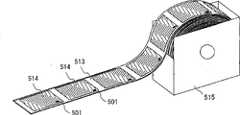
作为包含在元件衬底中的使用单晶半导体衬底或SOI衬底所形成的半导体元件的典型例子,有MOS晶体管、二极管、非易失性存储元件等的有源元件;以及电阻元件、电容元件等的无源元件。另外,作为晶体半导体衬底,最好有代表性地使用具有n型或p型导电类型的单晶硅衬底(硅片)、化合物半导体衬底(GaAs衬底、InP衬底、GaN衬底、SiC衬底、蓝宝石衬底、ZnSe衬底等)。另外,作为SOI衬底,可以使用所谓的SIMOX(注入氧隔离)衬底、或者使用智能剥离(Smart-Cut)法或ELTRAN法(Epitaxial Layer Transfer:佳能公司的注册商标)等所形成的SOI衬底。所述SIMOX衬底是通过在向镜面抛光片注入氧离子之后进行高温退火,从而从表面开始形成有一定深度的氧化层,同时消除在表面层所产生的缺陷而形成的。所述智能剥离法是利用通过注入氢离子而形成的微小空隙经过热处理而生长,从而劈开Si衬底而形成的。作为元件衬底的厚度,一般选为1μm以上且80μm以下,选为1μm以上且50μm以下较好,选为1μm以上且20μm以下更好,选为1μm以上且10μm以下更好,最好选为1μm以上且5μm以下。通过设定这种厚度,可以制造能够弯曲的半导体装置。另外,半导体装置的俯视面面积选为4mm2以上较好,最好选为9mm2以上。As typical examples of semiconductor elements formed using a single crystal semiconductor substrate or SOI substrate included in an element substrate, there are active elements such as MOS transistors, diodes, and nonvolatile memory elements; and resistive elements, capacitors passive components such as components. In addition, as a crystalline semiconductor substrate, it is preferable to typically use a single crystal silicon substrate (silicon wafer), a compound semiconductor substrate (GaAs substrate, InP substrate, GaN substrate) having an n-type or p-type conductivity type. , SiC substrate, sapphire substrate, ZnSe substrate, etc.). In addition, as the SOI substrate, a so-called SIMOX (implanted oxygen isolation) substrate, or an SOI substrate formed by using the Smart-Cut method or the ELTRAN method (Epitaxial Layer Transfer: a registered trademark of Canon Inc.) can be used. end. The SIMOX substrate is formed by high-temperature annealing after implanting oxygen ions into the mirror-polished sheet, thereby forming an oxide layer with a certain depth from the surface, and simultaneously eliminating defects generated in the surface layer. The smart lift-off method is formed by utilizing tiny voids formed by implanting hydrogen ions to grow through heat treatment, thereby cleaving the Si substrate. The thickness of the element substrate is generally 1 μm to 80 μm, preferably 1 μm to 50 μm, more preferably 1 μm to 20 μm, more preferably 1 μm to 10 μm, and most preferably 1 μm to 10 μm. 1 μm or more and 5 μm or less. By setting such a thickness, a bendable semiconductor device can be manufactured. In addition, the plan view surface area of the semiconductor device is preferably selected to be 4 mm2 or more, most preferably 9 mm2 or more.
图1表示本实施形态的半导体装置的截面图。FIG. 1 shows a cross-sectional view of a semiconductor device according to this embodiment.
在图1(A)所示的半导体装置1050中,纤维体113利用有机树脂114固定在包括MOS晶体管1060a、1060b的元件衬底1051的一个表面上。另外,设置密封层120以使其覆盖形成在元件衬底上的半导体元件。在此,将固定在元件衬底1051上的纤维体113及有机树脂114表示为密封层120。作为这种半导体装置1050的典型例子,有控制其他装置、或对数据进行计算及加工的微处理器(MPU)。MPU包括CPU、主存储器、控制器、接口、I/O端口等,并且它们可以由MOS晶体管、电阻元件、电容元件、布线等来构成。In
另外,元件衬底1051也可以具有光电二极管。典型地,在半导体衬底上形成如PN二极管、PIN二极管、雪崩二极管、肖特基二极管等的光电二极管。作为这种半导体装置的典型例子,有图像传感器。In addition, the
另外,在图1(B)所示的半导体装置1070中,纤维体113利用有机树脂114固定在包括存储元件1072以及MOS晶体管1060a、1060b的元件衬底1071的一个表面上。作为存储元件,包括:具有浮动栅或电荷存储层的非易失性存储元件、MOS晶体管以及与其连接的电容元件、包括MOS晶体管以及与其连接的铁电体层的电容元件、有机化合物层夹在一对电极之间的有机存储元件等。另外,作为包括这种存储元件的半导体装置,有如DRAM(动态随机存取存储器)、SRAM(静态随机存取存储器)、FeRAM(铁电随机存取存储器)、掩模ROM(只读存储器)、EPROM(电可编程只读存储器)、EEPROM(电可擦可编程只读存储器)、闪存等的存储装置。在此,作为存储元件1072,表示包括浮动栅极1073的非易失性存储元件。Further, in
另外,在图1(C)所示的半导体装置1080中,纤维体113利用有机树脂114固定在包括MOS晶体管1060a、1060b的元件衬底1081,以及与MOS晶体管1060a或1060b电连接的天线83的一个表面上。作为这种半导体装置的典型例子,有能够以无线方式收发信息的ID标签、IC标签、RF(射频)标签、无线标签、电子标签、RFID(射频识别)标签、IC卡、ID卡等(以下称为RFID)。另外,本发明的半导体装置包括:密封由MOS晶体管等构成的集成电路部和天线的嵌入体(inlet),以及将该嵌入体加工成封条状或卡片状后的该嵌体。另外,由于通过将半导体装置1080的俯视面面积设定为4mm2以上,最好设定为9mm2以上,从而可以将天线的面积形成得较大,因而可以获得与通信器的通信距离较长的RFID。In addition, in the
另外,元件衬底1051、1071、1081最好通过除去反面部的一部分而将其薄膜化。典型地说,一般元件衬底1051、1071、1081的厚度选为1μm以上且80μm以下,选为1μm以上且50μm以下较好,选为1μm以上且20μm以下更好,选为1μm至10μm更好,最好选为1μm以上且5μm以下。或者,也可以通过剥离半导体衬底的一部分来将元件衬底1051、1071、1081薄膜化。In addition, the
再者,除了在图1(A)至1(C)所示的元件衬底的一个表面上以外,还可以在另一个表面上利用有机树脂固定有纤维体113。换而言之,在元件衬底的两个表面上具有密封层,并且设置相互对向的一对密封层以从两面覆盖形成在元件衬底上的半导体元件。在图1(D)所示的半导体装置1090中,在图1(A)所示的半导体装置的元件衬底1051的一个表面上具有密封层120a,而在元件衬底1051的另一个表面上具有密封层120b。此时,虽然为了减少弯曲,密封层120a、120b最好选择由相同材质的纤维体及有机树脂来形成,但是在作为判别正面和反面而使用的用途时,未必是相同的材质。因为通过像这样固定浸渗在纤维体中的有机树脂,并且利用纤维体来支撑元件衬底的两面,因而可以减少半导体装置的弯曲,并且容易将该半导体装置安装到后述的层压膜或封条等上。Furthermore, besides one surface of the element substrate shown in FIGS. 1(A) to 1(C), the
设置在元件衬底的一个表面或两个面上的纤维体113是采用有机化合物或无机化合物的高强度纤维而够成的织造布或无纺布,并且完全覆盖整个元件衬底。作为高强度纤维,典型的是拉伸弹性模量高的纤维。或者是杨氏模量高的纤维。作为高强度纤维的典型例子,有聚乙烯醇类纤维、聚酯类纤维、聚酰胺类纤维、聚乙烯类纤维、芳族聚酰胺类纤维、聚对亚苯基苯并双噁唑纤维、玻璃纤维、或碳素纤维。作为玻璃纤维可以采用使用了E玻璃、S玻璃、D玻璃、Q玻璃等的玻璃纤维。另外,纤维体113也可以由一种上述高强度纤维来形成。另外,还可以由多种上述高强度纤维来形成。The
另外,纤维体113还可以由织造布或无纺布构成,该织造布是在经线及纬线使用纤维(单股线)束(以下称为线束)而编织构成的,该无纺布是使多种纤维的线束在任意或一个方向上堆积而构成的。若是织造布,可以适当地使用平纹织布、斜纹织布、缎纹织布等。In addition, the
线束的截面可以是圆形的,也可以是椭圆形的。作为线束,还可以采用通过高压水流、以液体为介质的高频振荡、连续超声波振动、以及利用滚筒的推压等而经过开纤加工后的线束。经过开纤加工后的线束变宽,并且可以减少在厚度方向上的单股线数目,而使线束的截面成为椭圆形或平板状。另外,因为使用弱捻纱线作为线束,所以容易将线束扁平化,而使线束的截面形状成为椭圆形或平板状。像这样,通过使用其截面是椭圆形或平板状的线束,可以使纤维体113的厚度变薄。因此,可以使密封层120的厚度变薄,从而可以制造薄型的半导体装置。当线束宽度为4μm以上且400μm以下,甚至为4μm以上且200μm以下的条件下确认了本发明的效果,并且在原理上可以进一步减小宽度。另外,当线束厚度为4μm以上且20μm以下的条件下确认了本发明的效果,并且在原理上可以进一步减小厚度,这些取决于纤维的材料。The cross-section of the wire harness can be circular or oval. As the wire harness, it is also possible to use a wire harness that has been subjected to fiber opening processing by high-pressure water flow, high-frequency vibration using a liquid as a medium, continuous ultrasonic vibration, and pressing with a roller. After fiber opening, the wire bundle becomes wider, and the number of single strands in the thickness direction can be reduced, so that the cross section of the wire bundle becomes oval or flat. In addition, since the weakly twisted yarn is used as the wire harness, it is easy to flatten the wire bundle, and the cross-sectional shape of the wire bundle becomes an ellipse or a flat plate. In this way, the thickness of the
在本说明书的附图中,表示纤维体113是使用截面为椭圆形的线束经过平纹编织后的织造布。另外,虽然MOS晶体管1060a、1060b比纤维体113的线束要大,但是也有MOS晶体管的大小比纤维体113的线束小的情况。In the drawings of this specification, it is shown that the
图8表示织造布的俯视图,该织造布是在经线及纬线上使用线束来编织纤维体113而构成的织物。FIG. 8 shows a plan view of a woven fabric formed by weaving
如图8(A)所示,纤维体113是编织隔开一定距离的经线113a以及隔开一定距离的纬线113b而构成的。在这种纤维体中具有不存在经线113a及纬线113b的区域(称为篮孔(basket hole)113c)。当使用这种纤维体113时,能够提高有机树脂浸渗在纤维体中的比例,从而可以提高纤维体113及元件衬底的紧密性。As shown in FIG. 8(A) , the
另外,如图8(B)所示,纤维体113也可以是经线113a及纬线113b的密度较高、且篮孔113c的比例较低的织造布。典型地,篮孔113c的大小最好小于局部推压的面积。典型地,最好是一边长为0.01mm以上且0.2mm以下的矩形。若纤维体113的篮孔113c的面积这样小,则即使在利用前端很细的构件(典型的为笔或铅笔等的书写工具)进行推压时,也可以用纤维体113整体吸收该压力。In addition, as shown in FIG. 8(B), the
另外,为了提高有机树脂向线束内部渗透的比例,还可以对线束进行表面处理。例如有为了使线束表面活性化的电晕放电处理、等离子体放电处理等。另外,还有使用了硅氧烷耦合剂、钛酸盐耦合剂的表面处理。In addition, in order to increase the rate of penetration of the organic resin into the interior of the wire harness, surface treatment may also be performed on the wire harness. For example, there are corona discharge treatment and plasma discharge treatment for activating the surface of the wire harness. In addition, there are surface treatments using silicone coupling agents and titanate coupling agents.
作为浸渗在纤维体113中、且密封元件衬底表面的有机树脂114,可以使用热固化树脂,该热固化树脂诸如环氧树脂、不饱和聚酯树脂、聚酰亚胺树脂、双马来酰亚胺三嗪树脂或氰酸酯树脂等。或者,还可以使用热可塑性树脂,该热可塑性树脂诸如聚苯醚树脂、聚醚酰亚胺树脂或氟树脂等。另外,也可以使用上述热可塑性树脂及上述热固化树脂中的多种。通过使用上述有机树脂,可以利用热处理将纤维体固定在元件衬底上。另外,有机树脂114的玻璃转移温度越高,越不容易由于受到局部推压而损坏,因而比较好。As the
另外,密封层120的厚度为10μm以上且100μm以下较好,最好为10μm以上且30μm以下。通过使用具有这种厚度的密封层,可以制造薄型且能够弯曲的半导体装置。In addition, the thickness of the
也可以使高导热填料在有机树脂114或线束中分散。作为高导热填料有氮化铝、氮化硼、氮化硅、矾土等。另外,作为高导热填料有如银、铜等的金属粒子。由于在有机树脂或线束中包含导电填料,而容易将在元件衬底中产生的热向外部放出,所以可以抑制半导体装置的蓄热,并且可以降低半导体装置的损坏。It is also possible to disperse highly thermally conductive fillers in the
另外,在图1(D)中,形成在元件衬底1051上的密封层120a的纤维体的经线或纬线的方向、与密封层120b的纤维体的经线或纬线的方向可以偏差在30度以上且60度以下,最好偏差在40度以上且50度以下。在这种情况下,由于设置在元件衬底正反面上的纤维体的拉伸方向在正反面上是不同的,所以当受到局部推压时的拉伸方向是各向同性的。因此,可以进一步地减少由于局部推压而引起的损坏。In addition, in FIG. 1(D), the direction of the warp or weft of the fiber body of the
在此,使用图2来表示本实施形态所示的半导体装置所具有的效果。Here, the effect of the semiconductor device shown in this embodiment is shown using FIG. 2 .
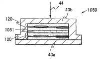
如图2(A)所示,在现有的半导体装置40中,使用粘接剂42a、42b并由薄膜43a、43b来密封包括利用单晶半导体衬底或SOI衬底所形成的半导体元件的元件衬底41。向这种半导体装置施加局部推压44。As shown in FIG. 2(A), in a conventional semiconductor device 40,
结果,如图2(B)所示,构成元件衬底41的层、粘接剂42a、42b、薄膜43a、43b分别延伸,在推压部上产生曲率半径较小的弯曲。结果,构成元件衬底41的半导体元件、布线等发生龟裂,从而导致半导体装置损坏。As a result, as shown in FIG. 2(B), the layers constituting the
然而,如图2(C)所示,在本实施形态所示的半导体装置1050中,在元件衬底1051的一个表面或两个表面上设置由包含有机树脂的纤维体所构成的密封层。形成纤维体的纤维的拉伸弹性模量高或杨氏模量高。因此,即使受到点压或线压等局部推压44,纤维也不会延伸,所推压的力会分散到纤维体整体,因而半导体装置整体弯曲。结果,即使受到局部推压,半导体装置中所产生的弯曲会成为比曲率半径大的弯曲,则构成元件衬底1051的半导体元件、布线等不会发生龟裂,并且能够减少半导体装置的损坏。However, as shown in FIG. 2(C), in the
另外,通过将元件衬底1051的厚度变薄,可以使半导体装置弯曲。由此,可以增大元件衬底1051的面积,并且使制造半导体装置的工序变得容易。另外,当该半导体装置是内部安装有天线的RFID的情况时,可以增加天线的大小。因此,可以制造通信距离较长的RFID。In addition, the semiconductor device can be bent by reducing the thickness of the
接着,下面来表示使用单晶半导体衬底或SOI衬底所形成的半导体元件的结构。Next, the structure of a semiconductor element formed using a single crystal semiconductor substrate or an SOI substrate is shown below.
图1(A)所示的MOS晶体管1060a由半导体衬底1052、栅极绝缘层1055a、栅极1056a构成。另外,MOS晶体管1060b由p井区1053、栅极绝缘层1055b、栅电极1056b构成。当半导体衬底1052是n型的情况时,形成注入了p型杂质的p井区1053。作为p型杂质,例如使用硼,并且以5×1015cm-3至1×1016cm-3左右的浓度来添加。通过形成p井区1053,可以在该区域中形成n沟道型晶体管。另外,添加在p井区1053中的p型杂质具有控制MOS晶体管的阈值电压的作用。形成在半导体衬底1052及p井区1053上的沟道形成区是在与栅电极1056a、1056b大致一致的区域中形成的,并且位于半导体衬底1052、形成在p井区1053中的低浓度杂质区1054d、1054e、或者一对杂质区域1054a、1054b之间。另外,可以使用p型半导体衬底来形成半导体衬底1052,并且将p井区1053作为添加了n型杂质的n井区。The
一对杂质区1054a、1054b是在MOS晶体管中作为源极及漏极来起作用的区域。通过大约以1×10¹⁹原子/cm3至1×1021原子/cm3的浓度分别添加n型杂质即磷或砷、以及p型杂质的硼来形成一对杂质区1054a、1054b。The pair of
在栅极1056a1056b的侧壁上形成间隔物1057a、1057b,从而获得在其端部防止漏电流的效果。另外,利用该间隔物1057a、1057b,能够在栅极1056a、1056b的沟道长度方向上的两端的下方形成低浓度杂质区1054d、1054e。该低浓度杂质区1054d、1054e作为低浓度漏极(LDD)来起作用。虽然低浓度杂质区1054d、1054e不是必需要的结构,但是,通过设置该区域,可以缓和漏极端部的电场,并且可以抑制MOS晶体管的恶化。
可以通过进行热处理使半导体衬底1052的表面氧化并利用氧化硅膜来形成栅极绝缘层1055a、1055b。另外,在通过热氧化法形成氧化硅膜之后,通过进行氮化处理使氧化硅膜的表面氮化,通过这样,能够利用氧化硅膜以及含有氧和氮的膜(氧氮化硅膜)的叠层结构形成栅极绝缘层1055a、1055b。栅极绝缘层1055a、1055b由厚度为5nm至50nm的氧化硅及氧氮化硅等的无机绝缘物来形成。另外,作为栅极绝缘层1055a、1055b,可以形成高介电常数物质(也称为high-k材料)即钽氧化物、氧化铪、氧化铪硅酸盐、氧化锆、氧化铝、氧化钛等的金属氧化物,或者氧化镧等的稀土氧化物。The
栅极1056a、1056b最好由从钽(Ta)、钨(W)、钛(Ti)、钼(Mo)、铬(Cr)、铌(Nb)等之中所选择的金属,或者以这些金属为主要成分的合金材料或化合物材料来形成。另外,还可以采用添加了磷等杂质元素的多晶硅。另外,也可以利用由一层或多层的金属氮化物层和上述金属层构成的叠层结构来形成该栅极。作为金属氮化物,可以使用氮化钨、氮化钼、或氮化钛。通过设置金属氮化物层,可以提高形成在金属氮化物层上的金属层的紧密性,并且防止金属层的剥离。The
绝缘层1059起到使MOS晶体管和作为布线的导电层绝缘的层间绝缘层的作用。通过CVD法或溅射法等,能够以:包含如氧化硅膜、氮化硅膜、氧氮化硅膜、氮氧化硅膜等的氧或氮的绝缘层;包含如DLC(类金刚石碳)等的碳层;由环氧、聚酰亚胺、聚酰胺、聚乙烯苯酚、苯并环丁烯、丙烯酸等的有机材料或者硅氧烷树脂等的硅氧烷材料所构成的单层或层叠结构,从而形成绝缘层1059。The insulating
导电层1061、1062作为布线、电线插头等起作用。通过CVD法或溅射法等,使用从铝(Al)、钨(W)、钛(Ti)、钽(Ta)、钼(Mo)、镍(Ni)、铂(Pt)、铜(Cu)、金(Au)、银(Ag)、锰(Mn)、钕(Nd)、碳(C)、硅(Si)之中所选的元素、或者以这些元素为主要成分的合金材料或化合物,并以单层或叠层的方式来形成导电层1061、1062。以铝为主要成分的合金材料相当于例如以铝为主要成分且含有镍的材料、或者以铝为主要成分且含有碳和硅中的一方或双方的合金材料。作为导电层1061、1062,例如可以采用阻挡膜、铝硅膜和阻挡膜的叠层结构、或者阻挡膜、铝硅膜、氮化钛膜和阻挡膜的叠层结构。另外,阻挡膜相当于由钛、钛的氮化物、钼或钼的氮化物所组成的薄膜。因为铝或者铝硅具有电阻置较低、并且价格低廉的特性,所以作为形成导电层1061、1062的材料是最合适的。此外,当在上层和下层设置阻挡膜时,可以防止铝或铝硅的小丘的产生。此外,当形成由高还原性的元素即钛所构成的阻挡膜时,即使可以在半导体衬底上得到较薄的自然氧化膜,通过还原该自然氧化膜,可以获得与半导体衬底的良好接触。The
另外,也可以在导电层1062、绝缘层1059上形成作为保护薄膜起作用的绝缘层1063。绝缘层1063是由氮化硅、氮氧化硅、氮化碳、DLC等来形成的。通过设置作为保护薄膜起作用的绝缘层1063,可以抑制水分从外部浸入MOS晶体管中,并且可以提高MOS晶体管以及半导体装置的电特性的可靠性。In addition, an insulating
另外,也可以在绝缘层1063上形成一组或多组的导电层以及与该导电层绝缘的绝缘层,从而作为多层结构。通过采用多层结构,可以实现高集成化。在这种情况下,作为与导电层绝缘的绝缘层,最好使用SiOF、SiOC、DLC、多孔二氧化硅等的介电常数大约为4以下的低介电常数材料来形成。另外,介电常数为4以下的低介电常数材料也被称为low-k材料,并且使用low-k材料所制成的薄膜也被称为low-k膜。这样,通过使用low-k材料来形成绝缘层,可以降低布线之间的电容,并且可以降低耗电量。In addition, one or more sets of conductive layers and insulating layers insulated from the conductive layers may be formed on the insulating
图1(B)所示的存储元件1072是由p井区1053、沟道氧化层1055c、浮动栅极1073、控制绝缘层1074、控制栅极1056c而构成的非易失性存储元件。The
作为沟道氧化层1055c,可以通过减压CVD法、等离子体CVD法、热氧化法等形成1nm至10nm厚、最好为1nm至5nm厚的氧化硅的单层或氧化硅和氮化硅的叠层结构。另外,可以通过利用等离子体处理使半导体层氧化或氮化,从而形成沟道氧化层。而且,还可以通过等离子体处理将利用等离子体CVD法所形成的氧化硅氧化或氮化。通过进行该等离子体处理所形成的绝缘层很细致且绝缘耐压高,并且可靠性很高。As the
浮动栅极1073可以由导电层、聚硅层、硅点等来形成。另外,还可以使用由氮化硅、氮化锗等所形成的电荷存储层来替代浮动栅极。The floating
作为控制栅极1074,通过减压CVD法或等离子体CVD法等形成氧化硅、氮化硅、氧氮化硅、氧化铝等的一层或多层。以1nm至20nm的厚度,最好以5nm至10nm的厚度来形成第二绝缘层22。As the
通过使用液滴喷射法(喷墨法、分配器法等)喷射含有诸如银(Ag)、金(Au)、铜(Cu)、镍(Ni)、铂(Pt)、钯(Pd)、钽(Ta)、钼(Mo)、以及钛(Ti)等之中的任一种及多种的金属粒子的液滴或糊剂并进行干燥和焙烧来形成图1(C)所示的天线83。通过使用液滴喷射法形成天线,可以减少工序数目,从而可以减少成本。By using a droplet discharge method (inkjet method, dispenser method, etc.) (Ta), molybdenum (Mo), and titanium (Ti) etc. in any one or a paste of metal particles and drying and firing to form the
另外,还可以使用丝网印刷法来形成天线83。在使用丝网印刷法的情况下,作为天线83的材料选择性地印刷将颗粒直径为几nm至几十μm的导电粒子溶解或分散在有机树脂中而形成的导电糊剂。作为导电粒子,可以使用从银(Ag)、金(Au)、铜(Cu)、镍(Ni)、铂(Pt)、钯(Pd)、钽(Ta)、钼(Mo)和钛(Ti)等之中选择的任一种及多种的金属粒子、卤化银的微粒,或分散性的纳米粒子。此外,作为包含在导电糊剂中的有机树脂,可以使用从作为金属粒子的结合剂、溶剂、分散剂或涂敷材起作用的有机树脂中的一种或多种。典型地,可以举出如环氧树脂和硅酮树脂等的有机树脂。此外,当形成导电层时,最好在挤出导电糊剂之后再进行焙烧。In addition, the
另外,天线83除了丝网印刷法以外,还可以使用凹版印刷等来形成,并且可以使用电镀法、溅射法等并由导电性材料来形成。In addition, the
另外,应用电磁耦合方式或者电磁感应方式(例如,13.56MHz频带)作为RFID的信号的传送方式。在利用由于磁场密度的变化而引起的电磁感应的情况下,可以将天线的俯视形状形成为环形(例如,环形天线)或者螺旋形(例如,螺旋天线)。In addition, an electromagnetic coupling method or an electromagnetic induction method (eg, 13.56 MHz band) is applied as a transmission method of RFID signals. In the case of utilizing electromagnetic induction due to changes in magnetic field density, the top view shape of the antenna may be formed into a loop (for example, a loop antenna) or a helical shape (for example, a helical antenna).
此外,也可以应用微波方式(例如UHF频带(860MHz至960MHz频带)、2.45GHz频带等)作为RFID的信号传送方式。在这种情况下,可以考虑用于信号传送的电磁波的波长,从而适当地设定天线的形状如长度等。In addition, a microwave method (for example, UHF frequency band (860 MHz to 960 MHz frequency band), 2.45 GHz frequency band, etc.) can also be applied as the signal transmission method of RFID. In this case, the shape of the antenna such as the length and the like can be appropriately set in consideration of the wavelength of the electromagnetic wave used for signal transmission.
图9(A)至9(D)表示能够应用微波方式的RFID的天线83的一个例子。例如,可以将天线的俯视形状形成为直线形(例如,偶极天线(参照图9A))、平坦的形状(例如贴片天线(参照图9B))、或者条带形(参照图9C、9D)等。此外,作为天线起作用的导电层的形状并不仅限于直线形,考虑到电磁波的波长,还可以以曲线形状、蛇行形状或者其组合的形状设置。9(A) to 9(D) show an example of an
在以下实施形态中,以RFID作为半导体装置的一个例子来举例说明本实施形态中所表示的半导体装置的制造方法。In the following embodiments, a method of manufacturing a semiconductor device shown in this embodiment will be described by taking RFID as an example of a semiconductor device.
(实施方式2)(Embodiment 2)
在本实施形态中,使用图3来表示高成品率地制造半导体装置的方法,其中该半导体装置即使受到来自外部的局部性压力也不容易损坏。In this embodiment, FIG. 3 is used to illustrate a method of manufacturing a semiconductor device that is not easily damaged even if it is subjected to local pressure from the outside with high yield.
如图3(A)所示,形成包括使用单晶半导体衬底或SOI衬底所形成的半导体元件的元件衬底1102及天线112。接着,在元件衬底1102及天线112上设置将有机树脂浸渗在纤维体中而构成的结构体115。另外,作为元件衬底1102的厚度,一般为1μm以上且80μm以下,为1μm以上且50μm以下较好,为1μm以上且20μm以下更好,为1μm以上且10μm以下更好,最好为1μm以上且5μm以下。通过设定这种厚度,可以制造能够弯曲的半导体装置。As shown in FIG. 3(A), an
在此,作为使用单晶半导体衬底或SOI衬底所形成的半导体元件的典型例子,表示实施方式1中所示的使用单晶半导体衬底而形成的MOS晶体管1060a、1060b。Here, the
另外,作为包括使用单晶半导体衬底或SOI衬底所形成的半导体元件的元件衬底1102,表示MOS晶体管1060a、1060b;覆盖MOS晶体管1060a、1060b的绝缘层106;通过绝缘层106与MOS晶体管1060a的半导体衬底及MOS晶体管1060b的p井区1053的源区和漏区连接的布线108、109;覆盖布线108、109以及绝缘层106的绝缘层111。另外,在元件衬底1102上形成通过绝缘层111与布线109连接的天线112。In addition, as an
绝缘层106作为使MOS晶体管和布线绝缘的层间绝缘层起作用。绝缘层106是通过溅射法、等离子体CVD法、涂敷法、印刷法等并且使用无机化合物以单层或多层形式而形成的。作为无机化合物的典型例子,有氧化硅、氮化硅、氧氮化硅、氮氧化硅等。另外,虽然这里采用了绝缘层106的单层结构,但可以采用叠层形式。这里,作为绝缘层106,通过涂敷法涂敷用有机溶剂稀释环氧树脂后而得到的组合物、再进行干燥和焙烧来形成绝缘层106。The insulating
布线108、109可以与实施形态1所示的导电层1061、1062同样地来形成。在此,按顺序层叠形成钛层、铝层、以及钛层,然后使用通过光刻工序所形成的抗蚀剂掩模而选择性地进行刻蚀,从而形成布线108、109。The
也可以在布线108、109上设置氮化硅、氮氧化硅、类金刚石碳、氮化碳等的保护层。通过设置保护层,可以抑制水分从外部进入MOS晶体管中,并且可以提高MOS晶体管及半导体装置的电特性的可靠性。A protective layer of silicon nitride, silicon oxynitride, diamond-like carbon, carbon nitride, or the like may be provided on the
绝缘层111通过采用与绝缘层106相同的形成方法及材料来形成。另外,绝缘层111是之后形成的天线的基底层。因此,绝缘层111的表面最好是平坦的。因此,绝缘层111最好是通过涂敷用有机溶剂稀释有机树脂后而得到的组合物、再进行干燥和焙烧来形成。另外,通过采用稀释感光树脂而得到的组合物来形成绝缘层111,由于工序数目比采用通过现有的光刻工序所形成的抗蚀剂掩模来进行刻蚀的工序要少,因此提高了成品率。在此,涂敷用有机溶剂稀释感光聚酰亚胺树脂而得到的组合物、并使它干燥,使用光掩模进行曝光,然后去除未固化部分并进行焙烧,从而形成绝缘层111。The insulating
天线112是采用与实施形态1所示的天线83相同的形成方法及材料来形成的。在此,在通过溅射法形成铝层之后,使用通过光刻工序所形成的抗蚀剂掩模且选择性地进行刻蚀,从而形成天线112。The
另外,元件衬底1102最好是通过除去反面部的一部分而被薄膜化的。作为部分地除去反面部的方法,有物理研磨及化学除去。物理研磨是当在半导体衬底的表面(形成半导体元件的一侧)贴合保护胶带之后,机械磨削半导体衬底的反面,并且通过化学机械研磨来研磨反面的方法。另外,化学除去包括:使用SF6、CF4等的气体的干刻蚀;使用氟酸·硝酸·醋酸混合液或氢氧化钾水溶液的干刻蚀。典型地,元件衬底1102的厚度一般为1μm以上且80μm以下,为1μm以上且50μm以下较好,为1μm以上且20μm以下更好,为1μm以上且10μm以下更好,最好为1μm以上且5μm以下。或者,也可以剥离半导体衬底的一部分而将其薄膜化,从而形成元件衬底1102。In addition, the
接着,在天线112上设置将有机树脂114浸渗在纤维体113中而构成的结构体115。这种结构体115也被称为预浸渍体。具体地说预浸渍体是:在将用有机溶剂稀释矩阵树脂而得到的组合物浸渗在纤维体中之后,通过进行干燥使有机溶剂挥发,从而使矩阵树脂半固化而构成的。结构体115的厚度为10μm以上且100μm以下较好,最好为10μm以上且30μm以下。通过使用这种厚度的结构体,可以制造薄型且能够弯曲的半导体装置。Next, the
接着,加热并压接结构体115,并使结构体115的有机树脂114可塑化或固化。另外,在有机树脂114是可塑性有机树脂的情况下,通过此后冷却至室温来使可塑化后的有机树脂固化。Next, the
通过加热及压合,有机树脂114均匀地遍布元件衬底1102及天线112的表面并使其固化。结果,如图3(B)所示,有机树脂114成为浸渗在纤维体113中并且固定在元件衬底1102和天线112的一个表面上的有机树脂121。另外,固定在元件衬底1102和天线112的一个表面上的有机树脂121,以及纤维体113与实施形态1同样地表示密封层120。在大气压下或减压下进行压接结构体115的工序。By heating and pressing, the
如上所示,可以制造半导体装置。另外,还可以在半导体衬底101一侧也形成密封层。在这种情况下,与图1(A)同样地在半导体衬底101上设置结构体,加热并压接结构体,从而使结构体的有机树脂可塑化或固化。在有机树脂具有可塑性的情况下,通过此后冷却至室温也使可塑化后的有机树脂固化。结果,如图3(C)所示,可以形成由纤维体113和浸渗在纤维体113中的有机树脂121所构成的密封层125。换而言之,可以制造在元件衬底1102的两面上设置有密封层120、125的半导体装置。As described above, a semiconductor device can be manufactured. In addition, a sealing layer may also be formed on the
另外,在元件衬底1102中包括多个半导体装置的情况下,还可以将元件衬底1102和密封层断开,从而切出多个半导体装置。通过进行这种工序可以制造多个半导体装置。当进行断开时,可以通过切割、划线、使用具有如剪刀或小刀等刃具的裁切机,或者激光切割法等选择性地进行断开。In addition, when a plurality of semiconductor devices are included in the
在本实施形态所示的半导体装置中,用有机树脂将包括使用单晶半导体衬底或SOI衬底所形成的半导体元件的元件衬底、以及纤维体固定在一起。由于纤维体将局部推压所产生的压力分散在整个纤维上,所以不容易受到局部性的压力。因此,构成半导体装置的布线和半导体元件不会延伸,而且半导体装置不容易损坏。另外,因为在元件衬底上固定由高强度纤维构成的纤维体,所以元件衬底在剥离工序中也不容易延伸。换而言之,可以抑制形成在元件衬底上的半导体元件和布线等延伸。因此,可以提高成品率。In the semiconductor device shown in this embodiment, an element substrate including a semiconductor element formed using a single crystal semiconductor substrate or an SOI substrate, and a fiber body are fixed together with an organic resin. Since the fiber body distributes the pressure generated by local pushing on the entire fiber, it is not easy to be subjected to local pressure. Therefore, wiring and semiconductor elements constituting the semiconductor device do not extend, and the semiconductor device is not easily damaged. In addition, since the fiber body made of high-strength fibers is fixed on the element substrate, the element substrate is not easily stretched in the peeling process. In other words, it is possible to suppress extension of semiconductor elements, wiring, and the like formed on the element substrate. Therefore, yield can be improved.
另外,通过将元件衬底的厚度变薄,可以使半导体装置弯曲。因此,可以增大元件衬底的面积。由此,制造半导体装置的工序变得容易。另外,在该半导体装置是内部安装有天线的RFID的情况下,可以增大天线的尺寸。因此,可以制造通信距离较长的RFID。In addition, the semiconductor device can be bent by reducing the thickness of the element substrate. Therefore, the area of the element substrate can be increased. Thereby, the process of manufacturing a semiconductor device becomes easy. In addition, when the semiconductor device is an RFID with an antenna mounted therein, the size of the antenna can be increased. Therefore, an RFID with a long communication distance can be manufactured.
(实施方式3)(Embodiment 3)
在本实施形态中,使用图4来说明比实施形态2更不容易损坏的半导体装置的制造方法。In this embodiment, a method of manufacturing a semiconductor device that is less prone to damage than in Embodiment 2 will be described using FIG. 4 .
如图4(A)所示,与实施形态1一样,形成包括使用单晶半导体衬底或SOI衬底所形成的半导体元件的元件衬底1102及天线112。接着,在元件衬底1102及天线112上设置结构体115,并且在结构体115上设置保护薄膜131。As shown in FIG. 4(A), as in the first embodiment, an
保护薄膜131最好由高强度材料来形成。作为高强度材料的典型例子,有聚乙烯醇类树脂、聚酯类树脂、聚酰亚胺类树脂、聚乙烯类树脂、芳族聚酰胺类树脂、聚对亚苯基苯并双噁唑树脂、玻璃树脂等。The
通过用高强度材料来形成保护薄膜131,与实施形态2相比,可以进一步抑制由于受到局部推压而导致的损坏。具体而言,当结构体115的纤维体113中没有分布经线及纬线的篮孔的面积大于受到局部压力的面积时,若对篮孔局部地施加负荷,则不能用结构体115的纤维体113来吸收该压力,从而导致直接地施加在元件衬底1102及天线112上。结果,元件衬底1102及天线112发生延伸,并且半导体元件或布线发生损坏。By forming the
然而,通过在结构体115上设置由高强度材料所形成的保护薄膜131,由于保护薄膜131整体吸收局部性的负荷,所以成为由于受到局部推压而导致的损坏较少的半导体装置。However, by providing the
接着,如图4(B)所示,与实施形态2一样,加热并压接结构体115来形成密封层120。另外,有机树脂121将保护薄膜131固定在元件衬底1102及天线112上。换而言之,密封层120将纤维体113及保护薄膜131固定在元件衬底1102及天线112上。另外,将包含在密封层120中的有机树脂121浸渗在纤维体113中。Next, as shown in FIG. 4(B), as in the second embodiment, the
然后,如图4(C)所示,在元件衬底1102的半导体衬底101上设置结构体,在结构体上设置保护薄膜,进行加热并压接,从而利用密封层125将保护薄膜141固定在元件衬底1102上。Then, as shown in FIG. 4(C), a structure is provided on the
另外,在图4(A)中,在保护薄膜131是热可塑性材料的情况下,也可以在元件衬底1102及天线112与结构体115之间设置保护薄膜薄131,并进行加热和压接。另外,在图4(C)中,在保护薄膜141是热可塑性材料的情况下,也可以在半导体衬底101和密封层125之间设置保护薄膜141,并进行加热和压接。在该结构中,也可以利用保护薄膜及密封层的纤维体来分散因受到局部推压而承受的负荷,从而能够减少损坏。In addition, in FIG. 4(A), in the case where the
另外,当元件衬底1102包括多个半导体装置时,还可以将元件衬底1102及密封层断开,从而切出多个半导体装置。通过进行这种工序可以制造多个半导体装置。In addition, when the
如上所述,可以制造由于受到局部推压而导致的损坏较少的半导体装置。As described above, it is possible to manufacture a semiconductor device that is less damaged due to partial pressing.
(实施方式4)(Embodiment 4)
在本实施形态中,使用图5及图6来说明一种半导体装置的制造方法,其中在该半导体装置中,在元件衬底不形成天线,并且将设置在其它的衬底上的天线与元件衬底连接。In this embodiment, a method of manufacturing a semiconductor device in which an antenna is not formed on an element substrate and an antenna and an element disposed on another substrate are combined is described using FIG. 5 and FIG. substrate connection.
如图5(A)所示,与实施形态2相同,形成包括使用单晶半导体衬底或SOI衬底所形成的半导体元件的元件衬底1151。接着在元件衬底1151上设置将有机树脂114浸渗在纤维体113中而得到的结构体。As shown in FIG. 5(A), as in the second embodiment, an
在此,作为元件衬底1151,如实施形态1所示,在半导体衬底101上形成MOS晶体管1060a、1060b。在MOS晶体管1060a、1060b上形成绝缘层106,并且形成通过绝缘层106与MOS晶体管的源区和漏区连接的布线108、109。在布线108、布线109和绝缘层106上形成绝缘层111,并且形成通过绝缘层111与布线109连接的电极盘152。Here, as
接着,与实施形态1相同,对设置在元件衬底1151上的结构体进行加热并压接,从而在元件衬底1151的一个表面上形成由有机树脂121和纤维体113所构成的密封层120。Next, as in the first embodiment, the structure provided on the
接着,除去密封层120的一部分,使电极盘152的一部分露出。在此,如图5(A)中的箭头所示那样,激光束从密封层120一侧向电极盘152照射以除去密封层120的一部分。另外,除了该方法以外,还可以使用一般的光刻工序除去密封层120的一部分以使电极盘152的一部分露出。Next, a part of the
接着,如图5(B)所示,在密封层120的开口部上形成连接端子161。连接端子161能够通过印刷法、液滴喷射法等来形成。作为连接端子161的材料,可以使用银(Ag)、金(Au)、铜(Cu)、镍(Ni)、铂(Pt)、钯(Pd)、钽(Ta)、钼(Mo)、以及钛(Ti)等中的任一种及多种的金属粒子;卤化银的微粒子;或分散纳米粒子。Next, as shown in FIG. 5(B),
然后,如图5(C)所示,使用粘接剂174将固定在元件衬底1151上的密封层120和形成有天线172的衬底171粘接在一起。此时,使用各向异性导电粘接剂173将形成在元件衬底1151上的连接端子161和天线172电连接起来。Then, as shown in FIG. 5(C), the
作为各向异性导电粘接剂173,是包含分散了的导电粒子(颗粒直径为几nm至几十μm)的粘接树脂,可以举出环氧树脂、酚醛树脂等。另外,导电粒子由从金、银、铜、钯、镍、碳、和铂中所选的一种元素或多种元素来形成。另外,也可以是具有这些元素的多层结构的粒子。而且,还可以采用在由树脂形成的粒子的表面上,形成有由从金、银、铜、钯、镍和铂中所选的一种元素或多种元素所形成的薄膜的导电粒子。再者,还可以使用CNT(碳纳米管)作为导电粒子。The anisotropic
作为天线172,可以适当地采用与实施形态1所示的天线83相同的材料及形成方法。As the
作为形成有天线172的衬底171,可以使用薄膜状的塑料衬底,例如聚对苯二甲酸乙二醇酯(PET)、聚醚砜(PES)、聚萘二甲酸乙二醇酯(PEN)、聚碳酸酯(PC)、尼龙、聚醚醚酮(PEEK)、聚砜(PSF)、聚醚酰亚胺(PEI)、聚芳酯(PAR)、聚对苯二甲酸丁二醇酯(PBT)等。As the
接着,如图6(A)所示,与实施形态1相同,在半导体衬底101的表面上设置结构体,加热并压接以在半导体衬底101上形成密封层125。Next, as shown in FIG. 6(A), similarly to the first embodiment, a structure is provided on the surface of the
接着,如图6(B)所示,也可以设置薄膜175,从而将形成有天线172的衬底171、密封层120、元件衬底1151、以及密封层125密封起来。作为薄膜,可以使用与形成有天线172的衬底171相同的薄膜。Next, as shown in FIG. 6(B), a
虽然在上述形态中表示了具有天线172的衬底171仅与元件衬底1151的一个表面粘接的半导体装置,但是也可以在元件衬底1151的两个面上分别粘接形成有天线的衬底。下面使用图7来说明其形态。Although the semiconductor device in which the
作为元件衬底1181,如实施形态1所示,在半导体衬底101上形成MOS晶体管1060a、1060b。在MOS晶体管1060a、1060b上形成绝缘层106,并且形成通过绝缘层106与MOS晶体管的源区和漏区连接的布线108、109。在布线108、109和绝缘层106上形成绝缘层111,并且形成通过绝缘层111与布线109连接的电极盘152及导电层153。As
接着,在半导体衬底101、绝缘层106、绝缘层111上形成贯通孔,并且在贯通孔的表面上形成贯通电极183。另外,贯通电极183与导电层153接触。另外,利用绝缘层184使贯通电极183和半导体衬底101绝缘。Next, through-holes are formed in the
然后,在该元件衬底1181的一个表面上,通过与图5(A)及(B)相同的工序来形成连接端子161。接着,通过与图5(C)相同的工序,并利用粘接剂174将形成有天线172的衬底171和设置在元件衬底1181的一个表面上的密封层120粘接起来。此时,使用各向异性导电粘接剂173将形成在元件衬底1181上的连接端子161和天线172电连接起来。另外,在元件衬底1181的另一个表面上设置密封层125。Then, on one surface of the
接着,当在元件衬底1181的半导体衬底101上设置结构体之后,进行加热和压接以形成密封层125。然后,为了形成与贯通电极183连接的连接端子,在密封层125的一部分上形成开口部。在此,从密封层125一侧向贯通电极183照射激光束185来形成开口部,从而使贯通电极183的一部分露出。Next, after the structural body is provided on the
接着,如图7(B)所示,形成连接端子186,以填充开口部。连接端子186可以用与连接端子161同样的方式来形成。Next, as shown in FIG. 7(B),
接着,如图7(C)所示,使用粘接剂194将密封层125和形成有天线192的衬底191粘接在一起,并且使用各向异性导电粘接剂193将连接端子186和天线192电连接起来。Next, as shown in FIG. 7(C), the
通过上述工序,可以制造在元件衬底的两面设置有天线的半导体装置。当将这种结构可以接收UHF频带的电波的RFID那样应用于具有对称结构的天线的半导体装置中时,因为可以减少半导体装置的大小,所以比较好。Through the above steps, it is possible to manufacture a semiconductor device in which antennas are provided on both surfaces of an element substrate. When such a structure is applied to a semiconductor device having an antenna having a symmetrical structure like RFID which can receive radio waves in the UHF band, it is preferable because the size of the semiconductor device can be reduced.
另外,当在元件衬底1151、1181中包括多个半导体装置时,还可以将元件衬底1151、1181、以及密封层断开,从而切出多个半导体装置。通过这种工序可以制造多个半导体装置。In addition, when a plurality of semiconductor devices are included in the
在本实施形态所示的半导体装置中,用有机树脂将包括使用单晶半导体衬底或SOI衬底所形成的半导体元件的元件衬底、以及纤维体固定在一起。由于纤维体将由于局部推压所产生的压力分散到纤维整体上,所以不容易受到局部性的压力。因此,构成半导体装置的布线和半导体元件不会延伸,而且半导体装置不容易损坏。另外,由于在元件衬底上固定有由高强度纤维所构成的纤维体,所以元件衬底在剥离工序中也不容易延伸。换而言之,可以抑制形成在元件衬底中的半导体元件和布线等发生延伸。因此,可以提高成品率。In the semiconductor device shown in this embodiment, an element substrate including a semiconductor element formed using a single crystal semiconductor substrate or an SOI substrate, and a fiber body are fixed together with an organic resin. Since the fiber body distributes the pressure generated by local pressing to the entire fiber, it is less likely to receive local pressure. Therefore, wiring and semiconductor elements constituting the semiconductor device do not extend, and the semiconductor device is not easily damaged. In addition, since the fiber body made of high-strength fibers is fixed on the element substrate, the element substrate is not easily stretched in the peeling process. In other words, it is possible to suppress extension of semiconductor elements, wirings, and the like formed in the element substrate. Therefore, yield can be improved.
另外,通过将元件衬底的厚度变薄,可以使半导体装置弯曲。因此,可以增大元件衬底的面积。因此,当将外部天线与元件衬底连接时,可以增大连接面积,并且可以容易进行制造半导体装置的工序。另外,当该半导体装置是内部安装有天线的RFID时,可以增加天线的大小。因此,可以制造通信距离较长的RFID。In addition, the semiconductor device can be bent by reducing the thickness of the element substrate. Therefore, the area of the element substrate can be increased. Therefore, when connecting the external antenna to the element substrate, the connection area can be increased, and the process of manufacturing the semiconductor device can be easily performed. In addition, when the semiconductor device is an RFID in which an antenna is mounted, the size of the antenna can be increased. Therefore, an RFID with a long communication distance can be manufactured.
(实施方式5)(Embodiment 5)
在本实施形态中,用图10来说明一种半导体装置,在该半导体装置中,实施方式1至4所示的包括使用单晶半导体衬底或SOI衬底所形成的半导体元件的元件衬底与印刷衬底连接。In this embodiment, a semiconductor device is described using FIG. connected to the printed substrate.
图10(A)表示本实施形态的半导体装置250的立体图。在半导体装置250中,在柔性印刷衬底上设置有实施方式1至4中所示的包括使用单晶半导体衬底或SOI衬底所形成的半导体元件的元件衬底。例如,在由聚酯、聚酰亚胺等形成的基极膜251上,设置有由铜、金、银、铝等形成的布线252。另外,在布线252上通过绝缘层来设置实施方式1至4中所示的包括使用单晶半导体衬底或SOI衬底所形成的半导体元件的元件衬底,以及密封层的叠层体253a、253b。另外,布线252及叠层体253a、253b通过形成在密封层的接触孔中的连接端子来连接。用保护薄膜254来覆盖基极薄膜251、布线252、以及叠层体253a、253b。另外,在半导体装置250的端部,切除保护薄膜254的一部分,从而使连接器等的外部电路和布线252露出。FIG. 10(A) shows a perspective view of a
通过密封层将元件衬底设置在布线上并且进行加热和压接,通过这样可以将元件衬底固定在布线及基极薄膜上。The element substrate can be fixed on the wiring and the base film by placing the element substrate on the wiring through the sealing layer, heating and pressure-bonding.
另外,虽然在这里表示了具有一层布线252的半导体装置,但还可以替代一层而采用多层布线结构。另外,也可以使用多个布线来夹住叠层体253a、253b。通过将布线设置为多层,可以提高安装密度。In addition, although a semiconductor device having one layer of
图10(B)表示本实施形态的半导体装置260的截面图。在半导体装置260中,在印刷衬底上设置有实施方式1至4中所示的包括使用单晶半导体衬底或SOI衬底所形成的半导体元件的元件衬底。例如,在核心层261的一个表面上设置有实施方式1至4中所示的包括使用单晶半导体衬底或SOI衬底形成的半导体元件的元件衬底262。另外,用贯通密封层263的通路孔264将核心层261,和实施方式1至4中所示的在包括使用单晶半导体衬底或SOI衬底所形成的半导体元件的元件衬底262上所具有的半导体元件或布线连接起来。FIG. 10(B) shows a cross-sectional view of a
另外,在元件衬底262上设置组合层265。形成在核心层261、元件衬底262中的半导体元件及布线等,通过形成在组合层265的有机树脂层266中的通路孔267,与形成在半导体装置260表面上的导体图形268连接。In addition, a build-
另外,在核心层261的另一个表面上设置有组合层269。In addition, a build-
另外,也可以使用导电糊剂或引线等安装构件272将电容器、线圈、电阻器、二极管等的芯片271安装在半导体装置260上。In addition,
在本实施方式的半导体装置中,在印刷衬底上具有:包括使用单晶半导体衬底或SOI衬底所形成的半导体元件的层。另外,利用使用了纤维体而构成的预浸渍体来将元件衬底设置在印刷衬底中。因此,因为用纤维体来分散压力,所以即使受到局部推压(点压、线压等)也可以减少由于安装工序和弯曲而导致的损坏。另外,可以实现高集成化。In the semiconductor device of the present embodiment, a layer including a semiconductor element formed using a single crystal semiconductor substrate or an SOI substrate is provided on the printed substrate. In addition, the element substrate is provided on the printed substrate using a prepreg formed using a fiber body. Therefore, since the fibrous body is used to disperse the pressure, damage due to the installation process and bending can be reduced even if it is locally pushed (point pressure, line pressure, etc.). In addition, high integration can be realized.
(实施方式6)(Embodiment 6)
在本实施形态中表示本发明的半导体装置的结构以及应用例子。在此,作为半导体装置的典型例子,对于RFID及存储装置进行说明。In this embodiment, the configuration and application examples of the semiconductor device of the present invention are shown. Here, an RFID and a storage device will be described as typical examples of semiconductor devices.
首先,对于本发明的半导体装置中的一种即RFID 501的电路结构例进行说明。图11表示RFID 501的方框电路图。First, a circuit configuration example of the
图11的RFID 501的规格以国际标准规格的ISO 15693为基准,是附近型RFID,且其通信信号频率为13.56MHz。另外,接收只对应于读取数据的指令,而发送的数据传送速率大约为13kHz,并且数据编码形式为曼彻斯特代码。The specification of
RFID 501的电路部412大致是由电源部460和信号处理部461构成的。电源部460具有整流电路462和保持电容器463。另外,还可以在电源部460中设置当从天线411接收到的功率过多时用于保护内部电路的保护电路部(也称为限制电路部),和用来控制是否使保护电路部工作的保护电路控制电路部。通过设置该电路部,可以防止在RFID与通信器之间的通信距离极短等的情况下、由于RFID接收大功率而产生的不良情况,而且可以提高RFID的可靠性。换而言之,可以使RFID正常地工作,而不导致RFID内部的元件退化以及RFID本身的损坏。The
另外,在此,最好具有利用无线通信方式使通信器与RFID进行信息收发的单元,例如举出读取信息的读取器、具有读取功能及写入功能的读取/写入器等。另外,还包括具有读取功能和写入功能中的一种或两种的手机或计算机等。In addition, here, it is preferable to have a unit for transmitting and receiving information between a communicator and an RFID using a wireless communication method, for example, a reader for reading information, a reader/writer with a reading function and a writing function, etc. . In addition, a mobile phone or a computer having one or both of a read function and a write function is also included.
整流电路462对用天线411所接收到的载波进行整流,从而产生直流电压。保持电容器463使由整流电路462所产生的直流电压平滑。将在电源部460中所产生的直流电压作为电源电压,并且提供给信号处理部461的各电路。The
信号处理部461具有:解调电路464、时钟产生/校正电路465、识别/判断电路466、存储控制器467、掩模ROM 468、编码电路469、以及调制电路470。The
解调电路464是对天线所接收到的信号进行解调的电路。将解调电路464所解调的接收信号输入到时钟产生/校正电路465和识别/判断电路466中。The
时钟产生/校正电路465具有:产生信号处理部461的工作所需的时钟信号、并对该时钟信号进行校正的功能。例如,时钟产生/校正电路465具有电压控制振荡电路(以下称为VCO(电压控制振荡器)电路),将VCO电路的输出作为反馈信号并与所提供的信号的相位进行比较,并利用负反馈来调节输出信号,从而使所提供的信号和反馈信号成为一定的相位。The clock generation/
识别/判断电路466识别并判断命令码。识别/判断电路466所识别并判断的命令码是帧结束信号(EOF、帧结束)、帧开始信号(SOF、帧开始)、标记、指令码、掩模长度(mask length)、掩模值(mask value)等。另外,识别/判断电路466还具有识别发送错误的循环冗余校验(CRC、cyclic redundancy check)的功能。The recognition/
存储控制器467根据用识别/判断电路466所处理的信号,从掩模ROM 468中读取数据。另外,掩模ROM468存储有ID等。通过安装掩模ROM 468,构成不能复制和窜改的读取专用的RFID501。可以通过将这种读取专用的RFID 501抄入纸中,从而能够提供防止伪造的纸。The
编码电路469对存储控制器467从掩模ROM 468中所读取的数据进行编码。编码后的数据用调制电路470进行调制。将用调制电路470所调制的数据作为载波从天线411发送出去。The
接着,表示RFID的使用例子。本发明的RFID可以用于任何纸介质以及薄膜介质中。特别地,本发明的RFID可以用于要求防止伪造的任何纸介质中。例如为纸币、户籍副本、居民卡、护照、驾驶执照、身份证、会员证、鉴定书、诊察券、月票、票据、支票、货票、提单、仓库证券、股票、债券、商品券、券、抵押证券等。Next, an example of use of RFID will be shown. The RFID of the present invention can be used in any paper medium as well as film medium. In particular, the RFID of the present invention can be used in any paper medium where counterfeiting prevention is required. For example, banknotes, household registration copies, resident cards, passports, driver's licenses, ID cards, membership cards, certificates, medical certificates, monthly tickets, bills, checks, bills of lading, warehouse securities, stocks, bonds, commodity certificates, coupons, mortgages securities, etc.
另外,由于通过实施本发明可以使纸介质及薄膜介质具有纸介质上视觉所示的信息以外的很多信息,因此,通过将本发明的RFID应用到商品签条等中,可以实现商品管理的电子系统化或者防止商品的盗窃。以下,使用图12来说明与本发明相关的纸的使用例子。In addition, since the paper medium and the film medium can have a lot of information other than the information visually shown on the paper medium by implementing the present invention, by applying the RFID of the present invention to commodity labels and the like, electronic control of commodity management can be realized. Systematize or prevent theft of goods. Hereinafter, an example of use of paper related to the present invention will be described using FIG. 12 .
图12(A)是使用了抄有本发明的RFID 501的纸的无记名债券类511的一个例子。虽然无记名债券类511包括邮票、票、券、入场券、商品券、书籍券、文具券、啤酒券、米券、各种礼物券、各种服务券等,然而当然不局限于这些。另外,图12(B)是使用了抄有与本发明相关的RFID501的纸的证书类512(例如,居民卡或户籍副本)的一个例子。Fig. 12 (A) has used an example of the
图12(C)是将本发明的RFID应用到签条的一个例子。在签条衬纸(剥离纸)513上,用抄有RFID501的纸来形成签条(ID封条)514。签条514被收纳在容器515内。在签条514上印刷有与该商品或服务相关的信息(商品名、牌子、商标、商标权人、销售人、制造人等)。而且,由于在RFID501中存储有该商品(或商品的种类)所固有ID号码,因此可以容易地发现伪造、侵犯知识产权如商标权及专利权等、不正当竞争等的违法行为。可以预先向RFID501内输入在商品的容器或标签上记不完的大量信息,例如,商品的产地、销售地、品质、原材料、功能、用途、数量、形状、价格、生产方法、使用方法、生产日期、使用日期、食品保质期限、使用指南、与商品相关的知识产权信息等。因此,客商和消费者可以使用简单的通信器来获取这些信息。另外,其结构是:生产者可以容易地重写及擦除等,而客商和消费者不能重写及消除等的结构。Fig. 12(C) is an example of applying the RFID of the present invention to a label. A label (ID seal) 514 is formed on the label backing paper (release paper) 513 with paper on which the
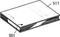
图12(D)表示由抄有RFID501的纸或薄膜所构成的标签516。通过使用抄有RFID501的纸或薄膜所制造的标签516,可以制造比使用了塑料框体的现有的ID标签更低廉的标签。图12(E)是将本发明的RFID用于封面的书籍517,其封面上抄有RFID501。FIG. 12(D) shows a
在商品上附加安装有本发明的半导体装置的一个例子即RFID的签条514或标签516,通过这样可以容易地管理商品。例如,在商品被盗窃时,可以通过跟踪商品的路径而迅速找出犯人。如此,通过将本发明的RFID作为ID标签,可以进行商品的履历管理或跟踪查询,例如履历管理包括该商品的原材料和原产地、制造及加工、流通、出售等。换而言之,可以实现商品可追溯性(traceability)。另外,通过使用本发明,可以以比传统更低的成本来实现商品的可追溯性管理系统。An
另外,本发明的半导体装置的一个例子即RFID不容易由于受到局部推压而损坏。因此,当对具有本发明的半导体装置的一个例子即RFID的纸介质及薄膜介质进行贴合和设置等处理时,可以使其弯曲,从而提高处理效率。另外,由于可以用书写工具在具有本发明的半导体装置的一个例子即RFID的纸介质及薄膜介质上写入信息,所以其用途很广泛。In addition, RFID, which is an example of the semiconductor device of the present invention, is less likely to be damaged by local pressure. Therefore, it is possible to bend paper media and film media having RFID, which is an example of the semiconductor device of the present invention, and to improve processing efficiency. In addition, since information can be written on paper media and film media having RFID, which is an example of the semiconductor device of the present invention, using a writing instrument, it is widely used.
接着,下面表示本发明的半导体装置的一个形态即存储装置的结构。在此,使用非易失性存储装置来作为存储装置的典型例子进行描述。Next, the structure of a memory device which is one form of the semiconductor device of the present invention is shown below. Here, description will be made using a nonvolatile memory device as a typical example of the memory device.
图13表示非易失性半导体存储装置的电路框图的一个例子。在非易失性半导体存储装置中,在相同的元件衬底上形成存储器单元阵列552和外围电路554。存储器单元阵列552具有如实施形态1所示的非易失性存储元件。外围电路554的结构如下所述。FIG. 13 shows an example of a circuit block diagram of a nonvolatile semiconductor memory device. In the nonvolatile semiconductor memory device, the
在存储器单元阵列552的周围设置:用于选择字线的行译码器562,和用于选择位线的列译码器564。地址通过地址缓冲器556传送到控制电路558中,并且内部行地址信号及内部列地址信号分别转送到行译码器562及列译码器564中。Around the
当进行数据的写入以及擦除时,使用使电源电位升压后的电位。因此,设置利用控制电路558并根据工作模式而进行控制的升压电路560。升压电路560的输出通过行译码器562或列译码器564提供到字线或位线中。从列译码器564中所输出的数据输入到读出放大器566中。由读出放大器566所读取的数据保存在数据缓冲器568中,然后利用来自控制电路558的控制对数据进行随机存取,并且通过数据输入/输出缓冲器570进行输出。写入数据通过数据输入/输出缓冲器570暂时保存在数据缓冲器568中,而且利用控制电路558的控制,将其转送到列译码器564中。When writing and erasing data, a potential obtained by boosting the power supply potential is used. Therefore, a
(实施方式7)(Embodiment 7)
在本实施形态中,下面表示使用了本发明的半导体装置后的电子设备。In this embodiment, electronic equipment using the semiconductor device of the present invention is shown below.
作为应用本发明的半导体装置的电子设备,可以举出摄像机或数字照相机等影像拍摄装置、护目镜型显示器(头戴显示器)、导航系统、音频再现装置(汽车立体声、音响组件等)、计算机、游戏机、便携式信息终端(移动计算机、手机、便携式游戏机或电子书籍等)、具有记录媒质的图像再现装置(具体地说,能够播放记录媒质比如DVD(数字通用光盘)等并且具有能够显示其图像的显示器的装置)等。在图14中表示这些电子设备的具体例子。Examples of electronic equipment to which the semiconductor device of the present invention is applied include video capture devices such as video cameras and digital cameras, goggle-type displays (head-mounted displays), navigation systems, audio reproduction devices (car stereos, audio components, etc.), computers, Game machines, portable information terminals (mobile computers, mobile phones, portable game machines, or electronic books, etc.), image reproduction devices with recording media (specifically, capable of playing recording media such as DVD (Digital Versatile Disc) etc. image display device), etc. Specific examples of these electronic devices are shown in FIG. 14 .
图14(A)和(B)表示一种数码相机。图14(B)为表示图14(A)的背面的图。该数字照相机包括框体2111、显示部2112、镜头2113、操作键2114、以及快门按钮2115等。在框体2111内部安装有:具有存储装置、MPU、图像传感器等的功能的本发明的半导体装置2116。14(A) and (B) show a digital camera. Fig. 14(B) is a view showing the back side of Fig. 14(A). This digital camera includes a housing 2111, a
此外,图14(C)表示一种手机,它是移动终端的一个典型例子。该手机包括框体2121、显示部2122、以及操作键2123等。另外,在该手机的内部还安装有:具有存储装置、MPU、图像传感器等的功能的本发明的半导体装置2125。In addition, FIG. 14(C) shows a mobile phone, which is a typical example of a mobile terminal. The mobile phone includes a housing 2121, a display unit 2122, operation keys 2123, and the like. In addition, the semiconductor device 2125 of the present invention having functions such as a storage device, an MPU, and an image sensor is mounted inside the mobile phone.
此外,图14(D)表示一种数字音响设备,它是音频装置的一个典型例子。图14(D)所示的数字音响设备包括:主体2130;显示部2131;具有存储装置、MPU、图像传感器等的功能的本发明的半导体装置2132;操作部2133;以及耳机2134等。In addition, Fig. 14(D) shows a digital audio equipment, which is a typical example of audio equipment. The digital audio equipment shown in FIG. 14(D) includes: a
另外,图14(E)表示电子书籍(也称为电子纸)。该电子书籍包括:主体2141;显示部2142;操作键2143;以及具有存储装置、MPU、图像传感器等的功能的本发明的半导体装置2144。另外,可以在主体2141的内部安装调制解调器,也可以构成能够以无线方式收发信息的结构。In addition, FIG. 14(E) shows an electronic book (also referred to as electronic paper). This electronic book includes: a
如上所述,本发明的半导体装置的应用范围很广泛,可以应用于其他电子设备中。As described above, the semiconductor device of the present invention has a wide range of applications and can be applied to other electronic devices.
Claims (34)
Translated fromChineseApplications Claiming Priority (2)
| Application Number | Priority Date | Filing Date | Title |
|---|---|---|---|
| JP2007-064052 | 2007-03-13 | ||
| JP2007064052 | 2007-03-13 |
Publications (2)
| Publication Number | Publication Date |
|---|---|
| CN101266954Atrue CN101266954A (en) | 2008-09-17 |
| CN101266954B CN101266954B (en) | 2013-03-06 |
Family
ID=39643902
Family Applications (1)
| Application Number | Title | Priority Date | Filing Date |
|---|---|---|---|
| CN2008100864215AExpired - Fee RelatedCN101266954B (en) | 2007-03-13 | 2008-03-12 | Semiconductor device and manufacturing method thereof |
Country Status (6)
| Country | Link |
|---|---|
| US (2) | US7808098B2 (en) |
| EP (2) | EP2372756A1 (en) |
| JP (1) | JP2008262547A (en) |
| KR (1) | KR101493295B1 (en) |
| CN (1) | CN101266954B (en) |
| TW (1) | TWI475748B (en) |
Cited By (3)
| Publication number | Priority date | Publication date | Assignee | Title |
|---|---|---|---|---|
| CN102214642A (en)* | 2011-06-03 | 2011-10-12 | 安徽省祁门县黄山电器有限责任公司 | Combined type high-power semiconductor chip |
| CN104716136A (en)* | 2013-12-17 | 2015-06-17 | 中芯国际集成电路制造(上海)有限公司 | Integrated circuit and manufacturing method thereof |
| CN104723640A (en)* | 2013-12-20 | 2015-06-24 | 英特尔公司 | Electronic fabric with incorporated chip and interconnect |
Families Citing this family (55)
| Publication number | Priority date | Publication date | Assignee | Title |
|---|---|---|---|---|
| EP1976000A3 (en)* | 2007-03-26 | 2009-05-13 | Semiconductor Energy Laboratory Co., Ltd. | Method for manufacturing semiconductor device |
| EP1976001A3 (en)* | 2007-03-26 | 2012-08-22 | Semiconductor Energy Laboratory Co., Ltd. | Method for manufacturing semiconductor device |
| TWI423519B (en)* | 2007-09-04 | 2014-01-11 | Mitsubishi Electric Corp | Radio frequency identification tag |
| WO2009031482A1 (en) | 2007-09-07 | 2009-03-12 | Semiconductor Energy Laboratory Co., Ltd. | Semiconductor device and method for manufacturing the same |
| JP5376961B2 (en)* | 2008-02-01 | 2013-12-25 | 株式会社半導体エネルギー研究所 | Semiconductor device |
| US8049292B2 (en)* | 2008-03-27 | 2011-11-01 | Semiconductor Energy Laboratory Co., Ltd. | Semiconductor device and method for manufacturing semiconductor device |
| WO2009139282A1 (en) | 2008-05-12 | 2009-11-19 | Semiconductor Energy Laboratory Co., Ltd. | Semiconductor device and method for manufacturing semiconductor device |
| WO2009142310A1 (en)* | 2008-05-23 | 2009-11-26 | Semiconductor Energy Laboratory Co., Ltd. | Semiconductor device and method for manufacturing the same |
| JP5473413B2 (en) | 2008-06-20 | 2014-04-16 | 株式会社半導体エネルギー研究所 | Wiring substrate manufacturing method, antenna manufacturing method, and semiconductor device manufacturing method |
| JP2010041045A (en)* | 2008-07-09 | 2010-02-18 | Semiconductor Energy Lab Co Ltd | Semiconductor device and method for producing the same |
| KR101588576B1 (en) | 2008-07-10 | 2016-01-26 | 가부시키가이샤 한도오따이 에네루기 켄큐쇼 | Light emitting device and electronic device |
| JP2010041040A (en)* | 2008-07-10 | 2010-02-18 | Semiconductor Energy Lab Co Ltd | Photoelectric conversion device and method for manufacturing photoelectric conversion device |
| JP5358324B2 (en)* | 2008-07-10 | 2013-12-04 | 株式会社半導体エネルギー研究所 | Electronic paper |
| JP5216716B2 (en) | 2008-08-20 | 2013-06-19 | 株式会社半導体エネルギー研究所 | Light emitting device and manufacturing method thereof |
| WO2010032602A1 (en) | 2008-09-18 | 2010-03-25 | Semiconductor Energy Laboratory Co., Ltd. | Semiconductor device |
| WO2010032611A1 (en)* | 2008-09-19 | 2010-03-25 | Semiconductor Energy Laboratory Co., Ltd. | Semiconductor device and method for manufacturing the same |
| WO2010035627A1 (en) | 2008-09-25 | 2010-04-01 | Semiconductor Energy Laboratory Co., Ltd. | Semiconductor device |
| KR101611643B1 (en) | 2008-10-01 | 2016-04-11 | 가부시키가이샤 한도오따이 에네루기 켄큐쇼 | Semiconductor device |
| JP5583951B2 (en)* | 2008-11-11 | 2014-09-03 | 株式会社半導体エネルギー研究所 | Method for manufacturing semiconductor device |
| CN102017099A (en)* | 2008-12-17 | 2011-04-13 | 松下电器产业株式会社 | Method for forming through electrode, and semiconductor device |
| KR101075753B1 (en)* | 2008-12-22 | 2011-10-24 | 삼성전자주식회사 | Antenna device and method for fabricating the same |
| JP5470054B2 (en)* | 2009-01-22 | 2014-04-16 | 株式会社半導体エネルギー研究所 | Semiconductor device |
| CN102460721B (en)* | 2009-06-05 | 2015-07-01 | 株式会社半导体能源研究所 | Photoelectric conversion device and method for manufacturing the same |
| CN102460722B (en)* | 2009-06-05 | 2015-04-01 | 株式会社半导体能源研究所 | Photoelectric conversion device and manufacturing method thereof |
| KR101732397B1 (en)* | 2009-06-05 | 2017-05-04 | 가부시키가이샤 한도오따이 에네루기 켄큐쇼 | Photoelectric conversion device and manufacturing method thereof |
| TWI474447B (en)* | 2009-06-29 | 2015-02-21 | Advanced Semiconductor Eng | Semiconductor package structure and enveloping method thereof |
| TWI517268B (en)* | 2009-08-07 | 2016-01-11 | 半導體能源研究所股份有限公司 | Method for manufacturing terminal structure and method for manufacturing electronic device |
| US9136286B2 (en) | 2009-08-07 | 2015-09-15 | Semiconductor Energy Laboratory Co., Ltd. | Display panel and electronic book |
| US8345435B2 (en)* | 2009-08-07 | 2013-01-01 | Semiconductor Energy Laboratory Co., Ltd. | Terminal structure and manufacturing method thereof, and electronic device and manufacturing method thereof |
| SG178061A1 (en) | 2009-08-25 | 2012-03-29 | Semiconductor Energy Lab | Method for reprocessing semiconductor substrate, method for manufacturing reprocessed semiconductor substrate, and method for manufacturing soi substrate |
| US8318588B2 (en) | 2009-08-25 | 2012-11-27 | Semiconductor Energy Laboratory Co., Ltd. | Method for reprocessing semiconductor substrate, method for manufacturing reprocessed semiconductor substrate, and method for manufacturing SOI substrate |
| KR101731809B1 (en) | 2009-10-09 | 2017-05-02 | 가부시키가이샤 한도오따이 에네루기 켄큐쇼 | Reprocessing method of semiconductor substrate, manufacturing method of reprocessed semiconductor substrate, and manufacturing method of soi substrate |
| JP5719560B2 (en)* | 2009-10-21 | 2015-05-20 | 株式会社半導体エネルギー研究所 | Manufacturing method of terminal structure |
| US8561909B2 (en)* | 2010-03-09 | 2013-10-22 | Skyworks Solutions, Inc. | RFID device having low-loss barium-based ceramic oxide |
| WO2011113278A1 (en)* | 2010-03-19 | 2011-09-22 | 上海集成电路研发中心有限公司 | Multi-system and multi-band radio frequency identification (rfid) antenna |
| US20120262660A1 (en)* | 2010-04-09 | 2012-10-18 | Sharp Kabushiki Kaisha | Display device |
| US8519509B2 (en) | 2010-04-16 | 2013-08-27 | Semiconductor Energy Laboratory Co., Ltd. | Semiconductor device and manufacturing method thereof |
| KR101679657B1 (en)* | 2010-09-29 | 2016-11-25 | 삼성전자주식회사 | Method for wafer level mold and wafer structure formed by the same |
| JP5715835B2 (en)* | 2011-01-25 | 2015-05-13 | 新光電気工業株式会社 | Semiconductor package and manufacturing method thereof |
| US9123529B2 (en) | 2011-06-21 | 2015-09-01 | Semiconductor Energy Laboratory Co., Ltd. | Method for reprocessing semiconductor substrate, method for manufacturing reprocessed semiconductor substrate, and method for manufacturing SOI substrate |
| JP2014135422A (en)* | 2013-01-11 | 2014-07-24 | Toyota Motor Corp | Semiconductor device manufacturing method |
| US10170315B2 (en) | 2013-07-17 | 2019-01-01 | Globalfoundries Inc. | Semiconductor device having local buried oxide |
| SG2013055348A (en)* | 2013-07-19 | 2015-02-27 | Kok Ann Wong | A contactless smart chip for biometric tracking |
| US9252272B2 (en) | 2013-11-18 | 2016-02-02 | Globalfoundries Inc. | FinFET semiconductor device having local buried oxide |
| JP2015216072A (en) | 2014-05-13 | 2015-12-03 | 株式会社ジャパンディスプレイ | Organic EL device and manufacturing method thereof |
| WO2016018585A1 (en)* | 2014-07-31 | 2016-02-04 | 3M Innovative Properties Company | Rfid tag on stretchable substrate |
| WO2016018777A2 (en) | 2014-07-31 | 2016-02-04 | 3M Innovative Properties Company | Rfid tag on flexible substrate |
| US20160379943A1 (en)* | 2015-06-25 | 2016-12-29 | Skyworks Solutions, Inc. | Method and apparatus for high performance passive-active circuit integration |
| US10615352B2 (en)* | 2016-01-25 | 2020-04-07 | Toray Industries, Inc. | n-Type semiconductor element, complementary type semiconductor device and method for manufacturing same, and wireless communication device in which same is used |
| US10581177B2 (en) | 2016-12-15 | 2020-03-03 | Raytheon Company | High frequency polymer on metal radiator |
| US11088467B2 (en) | 2016-12-15 | 2021-08-10 | Raytheon Company | Printed wiring board with radiator and feed circuit |
| US10541461B2 (en) | 2016-12-16 | 2020-01-21 | Ratheon Company | Tile for an active electronically scanned array (AESA) |
| US10361485B2 (en) | 2017-08-04 | 2019-07-23 | Raytheon Company | Tripole current loop radiating element with integrated circularly polarized feed |
| CN112585812B (en)* | 2018-08-24 | 2023-07-25 | 京瓷株式会社 | Resonant structure, antenna, wireless communication module, and wireless communication device |
| CN114023781B (en)* | 2021-10-08 | 2023-06-16 | 业成科技(成都)有限公司 | Curved surface electronic device and manufacturing method thereof |
Family Cites Families (70)
| Publication number | Priority date | Publication date | Assignee | Title |
|---|---|---|---|---|
| DE69032210D1 (en) | 1989-01-25 | 1998-05-07 | Asahi Chemical Ind | PRE-IMPREGNATED COMPOSITE MOLDS AND PRODUCTION OF A COMPOSITE MOLD |
| DE3907757A1 (en) | 1989-03-10 | 1990-09-13 | Mtu Muenchen Gmbh | PROTECTIVE FILM |
| JPH03125411A (en) | 1989-10-09 | 1991-05-28 | Asmo Co Ltd | Magnetizer |
| US5888609A (en)* | 1990-12-18 | 1999-03-30 | Valtion Teknillinen Tutkimuskeskus | Planar porous composite structure and method for its manufacture |
| JPH05190582A (en) | 1992-01-08 | 1993-07-30 | Oki Electric Ind Co Ltd | Resin sealed semiconductor device and manufacture thereof |
| JP3125411B2 (en) | 1992-02-21 | 2001-01-15 | 株式会社日立製作所 | Liquid crystal display |
| JP3578466B2 (en) | 1992-04-14 | 2004-10-20 | ユニチカ株式会社 | Inorganic fiber woven fabric for reinforcement and multilayer printed wiring board using the same |
| JPH077246A (en)* | 1993-06-17 | 1995-01-10 | Kobe Steel Ltd | Manufacture of in-molded product containing electronic component constituting material |
| DE69504336T2 (en) | 1994-05-27 | 1999-01-21 | Ake Chatel-St-Denis Gustafson | METHOD FOR PRODUCING AN ELECTRONIC MODULE AND MODULE PRODUCED BY THIS METHOD |
| TW371285B (en) | 1994-09-19 | 1999-10-01 | Amp Akzo Linlam Vof | Foiled UD-prepreg and PWB laminate prepared therefrom |
| JP3364081B2 (en) | 1995-02-16 | 2003-01-08 | 株式会社半導体エネルギー研究所 | Method for manufacturing semiconductor device |
| JP3406727B2 (en) | 1995-03-10 | 2003-05-12 | 株式会社半導体エネルギー研究所 | Display device |
| US5757456A (en) | 1995-03-10 | 1998-05-26 | Semiconductor Energy Laboratory Co., Ltd. | Display device and method of fabricating involving peeling circuits from one substrate and mounting on other |
| JPH08321679A (en)* | 1995-05-24 | 1996-12-03 | Nec Corp | Multilayer printed wiring board |
| JPH10129165A (en) | 1996-03-15 | 1998-05-19 | Hitachi Maxell Ltd | Information carrier and method of manufacturing the same |
| US6482495B1 (en) | 1996-09-04 | 2002-11-19 | Hitachi Maxwell, Ltd. | Information carrier and process for production thereof |
| JPH1092980A (en)* | 1996-09-13 | 1998-04-10 | Toshiba Corp | Wireless card and method of manufacturing the same |
| JPH10209340A (en)* | 1997-01-16 | 1998-08-07 | Toray Ind Inc | Ic sealing frame and its manufacture |
| JP3322256B2 (en)* | 1997-01-31 | 2002-09-09 | 株式会社デンソー | IC card manufacturing method |
| JP3193344B2 (en)* | 1998-05-25 | 2001-07-30 | 東レ・デュポン株式会社 | Surface treatment agent for aramid fiber, surface-treated aramid fiber, surface treatment method for aramid fiber, and fiber-reinforced composite material |
| JP2004078991A (en) | 1998-12-17 | 2004-03-11 | Hitachi Ltd | Semiconductor device and method of manufacturing the same |
| TW484101B (en) | 1998-12-17 | 2002-04-21 | Hitachi Ltd | Semiconductor device and its manufacturing method |
| US6224965B1 (en)* | 1999-06-25 | 2001-05-01 | Honeywell International Inc. | Microfiber dielectrics which facilitate laser via drilling |
| JP4423779B2 (en) | 1999-10-13 | 2010-03-03 | 味の素株式会社 | Epoxy resin composition, adhesive film and prepreg using the composition, multilayer printed wiring board using the same, and method for producing the same |
| US6370013B1 (en)* | 1999-11-30 | 2002-04-09 | Kyocera Corporation | Electric element incorporating wiring board |
| JP3675688B2 (en) | 2000-01-27 | 2005-07-27 | 寛治 大塚 | Wiring board and manufacturing method thereof |
| JP4884592B2 (en) | 2000-03-15 | 2012-02-29 | 株式会社半導体エネルギー研究所 | Method for manufacturing light emitting device and method for manufacturing display device |
| JP2002198658A (en)* | 2000-12-26 | 2002-07-12 | Kyocera Corp | Prepreg, method of manufacturing the same, and method of manufacturing wiring board using the same |
| JP4027740B2 (en) | 2001-07-16 | 2007-12-26 | 株式会社半導体エネルギー研究所 | Method for manufacturing semiconductor device |
| TW564471B (en) | 2001-07-16 | 2003-12-01 | Semiconductor Energy Lab | Semiconductor device and peeling off method and method of manufacturing semiconductor device |
| JP2003049388A (en) | 2001-08-08 | 2003-02-21 | Du Pont Toray Co Ltd | Cloth made of flattened aramid fiber |
| CN100380673C (en) | 2001-11-09 | 2008-04-09 | 株式会社半导体能源研究所 | Light emitting device and manufacturing method thereof |
| KR100430001B1 (en) | 2001-12-18 | 2004-05-03 | 엘지전자 주식회사 | Manufacturing method of multi-layer pcb, pad fabricating method of multi-layer pcb, semiconductor pkg manufacturing method using multi-layer pcb |
| EP1514307A1 (en)* | 2002-06-19 | 2005-03-16 | Sten Bjorsell | Electronics circuit manufacture |
| US7485489B2 (en) | 2002-06-19 | 2009-02-03 | Bjoersell Sten | Electronics circuit manufacture |
| DE10234246A1 (en)* | 2002-07-27 | 2004-02-05 | Tesa Ag | Pressure-sensitive adhesive material for bonding transparent substrates, e.g. in liquid crystal displays and other optical applications, comprises block copolymers with blocks of different refractive index |
| JP2004140267A (en) | 2002-10-18 | 2004-05-13 | Semiconductor Energy Lab Co Ltd | Semiconductor device and manufacturing method thereof |
| JP2004356569A (en)* | 2003-05-30 | 2004-12-16 | Shinko Electric Ind Co Ltd | Package for semiconductor device |
| JP4828088B2 (en) | 2003-06-05 | 2011-11-30 | 凸版印刷株式会社 | IC tag |
| JP4540359B2 (en) | 2004-02-10 | 2010-09-08 | シャープ株式会社 | Semiconductor device and manufacturing method thereof |
| JP4424044B2 (en)* | 2004-04-09 | 2010-03-03 | 住友ベークライト株式会社 | Transparent composite sheet and display element using the same |
| EP1589797A3 (en)* | 2004-04-19 | 2008-07-30 | Matsushita Electric Industrial Co., Ltd. | Manufacturing method of laminated substrate, and manufacturing apparatus of semiconductor device for module and laminated substrate for use therein |
| KR20060045208A (en) | 2004-11-12 | 2006-05-17 | 삼성테크윈 주식회사 | Circuit board for semiconductor package and manufacturing method thereof |
| JP5072217B2 (en) | 2004-11-22 | 2012-11-14 | 株式会社半導体エネルギー研究所 | Method for manufacturing semiconductor device |
| US7736964B2 (en) | 2004-11-22 | 2010-06-15 | Semiconductor Energy Laboratory Co., Ltd. | Semiconductor device, and method for manufacturing the same |
| JP2006192745A (en)* | 2005-01-14 | 2006-07-27 | Toray Ind Inc | Reinforcing fiber base material, preform, fiber reinforced resin molded product and its manufacturing method |
| JP4467449B2 (en)* | 2005-02-25 | 2010-05-26 | 旭化成イーマテリアルズ株式会社 | Substrate reinforcing fiber fabric, prepreg using the reinforcing fiber fabric, and printed wiring board substrate |
| US7566633B2 (en)* | 2005-02-25 | 2009-07-28 | Semiconductor Energy Laboratory Co., Ltd. | Semiconductor device and method for manufacturing the same |
| US20060202269A1 (en)* | 2005-03-08 | 2006-09-14 | Semiconductor Energy Laboratory Co., Ltd. | Wireless chip and electronic appliance having the same |
| JP5127161B2 (en)* | 2005-05-30 | 2013-01-23 | 株式会社半導体エネルギー研究所 | Semiconductor device |
| CN101228630B (en) | 2005-05-30 | 2011-10-05 | 株式会社半导体能源研究所 | Semiconductor device |
| JP4827618B2 (en)* | 2005-05-31 | 2011-11-30 | 株式会社半導体エネルギー研究所 | Method for manufacturing antenna, method for manufacturing semiconductor device |
| US7465674B2 (en) | 2005-05-31 | 2008-12-16 | Semiconductor Energy Laboratory Co., Ltd. | Manufacturing method of semiconductor device |
| WO2006129817A1 (en) | 2005-05-31 | 2006-12-07 | Semiconductor Energy Laboratory Co., Ltd. | Semiconductor device, manufacturing method thereof, and manufacturing method of antenna |
| JP4704959B2 (en)* | 2005-05-31 | 2011-06-22 | 株式会社半導体エネルギー研究所 | Product management method and dangerous goods management method |
| KR101216125B1 (en) | 2005-05-31 | 2012-12-27 | 가부시키가이샤 한도오따이 에네루기 켄큐쇼 | semiconductor device |
| JP5057703B2 (en) | 2005-05-31 | 2012-10-24 | 株式会社半導体エネルギー研究所 | Method for manufacturing semiconductor device |
| JP2007036216A (en)* | 2005-06-24 | 2007-02-08 | Semiconductor Energy Lab Co Ltd | Semiconductor device and wireless communication system |
| WO2006137573A1 (en) | 2005-06-24 | 2006-12-28 | Semiconductor Energy Laboratory Co., Ltd. | Semiconductor device and wireless communication system |
| US7727859B2 (en) | 2005-06-30 | 2010-06-01 | Semiconductor Energy Laboratory Co., Ltd | Semiconductor device and manufacturing method thereof |
| US7685706B2 (en)* | 2005-07-08 | 2010-03-30 | Semiconductor Energy Laboratory Co., Ltd | Method of manufacturing a semiconductor device |
| JP2007064052A (en) | 2005-08-30 | 2007-03-15 | Sanden Corp | Hybrid compressor |
| US7700463B2 (en) | 2005-09-02 | 2010-04-20 | Semiconductor Energy Laboratory Co., Ltd. | Method for manufacturing semiconductor device |
| TWI431726B (en) | 2006-06-01 | 2014-03-21 | Semiconductor Energy Lab | Non-volatile semiconductor memory device |
| EP2038818B1 (en) | 2006-06-26 | 2014-10-15 | Semiconductor Energy Laboratory Co., Ltd. | Paper including semiconductor device and manufacturing method thereof |
| EP1970951A3 (en) | 2007-03-13 | 2009-05-06 | Semiconductor Energy Laboratory Co., Ltd. | Semiconductor device and manufacturing method thereof |
| EP1976000A3 (en) | 2007-03-26 | 2009-05-13 | Semiconductor Energy Laboratory Co., Ltd. | Method for manufacturing semiconductor device |
| EP1976001A3 (en) | 2007-03-26 | 2012-08-22 | Semiconductor Energy Laboratory Co., Ltd. | Method for manufacturing semiconductor device |
| JP5248240B2 (en) | 2007-08-30 | 2013-07-31 | 株式会社半導体エネルギー研究所 | Semiconductor device |
| WO2009031482A1 (en) | 2007-09-07 | 2009-03-12 | Semiconductor Energy Laboratory Co., Ltd. | Semiconductor device and method for manufacturing the same |
- 2008
- 2008-03-03EPEP11005367Apatent/EP2372756A1/ennot_activeWithdrawn
- 2008-03-03EPEP20080003900patent/EP1970952A3/ennot_activeWithdrawn
- 2008-03-07USUS12/073,613patent/US7808098B2/ennot_activeExpired - Fee Related
- 2008-03-10TWTW097108347Apatent/TWI475748B/ennot_activeIP Right Cessation
- 2008-03-12CNCN2008100864215Apatent/CN101266954B/ennot_activeExpired - Fee Related
- 2008-03-12JPJP2008062133Apatent/JP2008262547A/ennot_activeWithdrawn
- 2008-03-13KRKR20080023223Apatent/KR101493295B1/ennot_activeExpired - Fee Related
- 2010
- 2010-09-29USUS12/892,961patent/US8558370B2/ennot_activeExpired - Fee Related
Cited By (7)
| Publication number | Priority date | Publication date | Assignee | Title |
|---|---|---|---|---|
| CN102214642A (en)* | 2011-06-03 | 2011-10-12 | 安徽省祁门县黄山电器有限责任公司 | Combined type high-power semiconductor chip |
| CN102214642B (en)* | 2011-06-03 | 2012-10-10 | 安徽省祁门县黄山电器有限责任公司 | Combined type high-power semiconductor chip |
| CN104716136A (en)* | 2013-12-17 | 2015-06-17 | 中芯国际集成电路制造(上海)有限公司 | Integrated circuit and manufacturing method thereof |
| CN104716136B (en)* | 2013-12-17 | 2018-02-06 | 中芯国际集成电路制造(上海)有限公司 | A kind of integrated circuit and its manufacture method |
| CN104723640A (en)* | 2013-12-20 | 2015-06-24 | 英特尔公司 | Electronic fabric with incorporated chip and interconnect |
| US9736936B2 (en) | 2013-12-20 | 2017-08-15 | Intel Corporation | Electronic fabric with incorporated chip and interconnect |
| US10201081B2 (en) | 2013-12-20 | 2019-02-05 | Intel Corporation | Electronic fabric with incorporated chip and interconnect |
Also Published As
| Publication number | Publication date |
|---|---|
| KR20080084666A (en) | 2008-09-19 |
| TWI475748B (en) | 2015-03-01 |
| TW200903898A (en) | 2009-01-16 |
| US20110024853A1 (en) | 2011-02-03 |
| KR101493295B1 (en) | 2015-02-16 |
| CN101266954B (en) | 2013-03-06 |
| US8558370B2 (en) | 2013-10-15 |
| EP2372756A1 (en) | 2011-10-05 |
| JP2008262547A (en) | 2008-10-30 |
| US20080224940A1 (en) | 2008-09-18 |
| EP1970952A2 (en) | 2008-09-17 |
| EP1970952A3 (en) | 2009-05-06 |
| US7808098B2 (en) | 2010-10-05 |
Similar Documents
| Publication | Publication Date | Title |
|---|---|---|
| CN101266954A (en) | Semiconductor device and manufacturing method thereof | |
| TWI442513B (en) | Semiconductor device manufacturing method | |
| CN103258800B (en) | Semiconductor device and manufacturing method thereof | |
| CN101276743B (en) | Method for manufacturing semiconductor device | |
| CN101803008B (en) | Semiconductor device and method for manufacturing the same | |
| JP2010021351A (en) | Semiconductor apparatus |
Legal Events
| Date | Code | Title | Description |
|---|---|---|---|
| C06 | Publication | ||
| PB01 | Publication | ||
| C10 | Entry into substantive examination | ||
| SE01 | Entry into force of request for substantive examination | ||
| C14 | Grant of patent or utility model | ||
| GR01 | Patent grant | ||
| CF01 | Termination of patent right due to non-payment of annual fee | Granted publication date:20130306 Termination date:20210312 | |
| CF01 | Termination of patent right due to non-payment of annual fee |