CN101261984A - Semiconductor assembly packaging structure and method thereof - Google Patents
Semiconductor assembly packaging structure and method thereofDownload PDFInfo
- Publication number
- CN101261984A CN101261984ACNA200810083485XACN200810083485ACN101261984ACN 101261984 ACN101261984 ACN 101261984ACN A200810083485X ACNA200810083485X ACN A200810083485XACN 200810083485 ACN200810083485 ACN 200810083485ACN 101261984 ACN101261984 ACN 101261984A
- Authority
- CN
- China
- Prior art keywords
- die
- substrate
- layer
- redistribution layer
- dielectric layer
- Prior art date
- Legal status (The legal status is an assumption and is not a legal conclusion. Google has not performed a legal analysis and makes no representation as to the accuracy of the status listed.)
- Pending
Links
Images


Classifications
- H—ELECTRICITY
- H01—ELECTRIC ELEMENTS
- H01L—SEMICONDUCTOR DEVICES NOT COVERED BY CLASS H10
- H01L25/00—Assemblies consisting of a plurality of semiconductor or other solid state devices
- H01L25/50—Multistep manufacturing processes of assemblies consisting of devices, the devices being individual devices of subclass H10D or integrated devices of class H10
- H—ELECTRICITY
- H01—ELECTRIC ELEMENTS
- H01L—SEMICONDUCTOR DEVICES NOT COVERED BY CLASS H10
- H01L23/00—Details of semiconductor or other solid state devices
- H01L23/48—Arrangements for conducting electric current to or from the solid state body in operation, e.g. leads, terminal arrangements ; Selection of materials therefor
- H—ELECTRICITY
- H01—ELECTRIC ELEMENTS
- H01L—SEMICONDUCTOR DEVICES NOT COVERED BY CLASS H10
- H01L24/00—Arrangements for connecting or disconnecting semiconductor or solid-state bodies; Methods or apparatus related thereto
- H01L24/01—Means for bonding being attached to, or being formed on, the surface to be connected, e.g. chip-to-package, die-attach, "first-level" interconnects; Manufacturing methods related thereto
- H01L24/18—High density interconnect [HDI] connectors; Manufacturing methods related thereto
- H01L24/19—Manufacturing methods of high density interconnect preforms
- H—ELECTRICITY
- H01—ELECTRIC ELEMENTS
- H01L—SEMICONDUCTOR DEVICES NOT COVERED BY CLASS H10
- H01L24/00—Arrangements for connecting or disconnecting semiconductor or solid-state bodies; Methods or apparatus related thereto
- H01L24/01—Means for bonding being attached to, or being formed on, the surface to be connected, e.g. chip-to-package, die-attach, "first-level" interconnects; Manufacturing methods related thereto
- H01L24/18—High density interconnect [HDI] connectors; Manufacturing methods related thereto
- H01L24/23—Structure, shape, material or disposition of the high density interconnect connectors after the connecting process
- H01L24/24—Structure, shape, material or disposition of the high density interconnect connectors after the connecting process of an individual high density interconnect connector
- H—ELECTRICITY
- H01—ELECTRIC ELEMENTS
- H01L—SEMICONDUCTOR DEVICES NOT COVERED BY CLASS H10
- H01L24/00—Arrangements for connecting or disconnecting semiconductor or solid-state bodies; Methods or apparatus related thereto
- H01L24/80—Methods for connecting semiconductor or other solid state bodies using means for bonding being attached to, or being formed on, the surface to be connected
- H01L24/82—Methods for connecting semiconductor or other solid state bodies using means for bonding being attached to, or being formed on, the surface to be connected by forming build-up interconnects at chip-level, e.g. for high density interconnects [HDI]
- H—ELECTRICITY
- H01—ELECTRIC ELEMENTS
- H01L—SEMICONDUCTOR DEVICES NOT COVERED BY CLASS H10
- H01L24/00—Arrangements for connecting or disconnecting semiconductor or solid-state bodies; Methods or apparatus related thereto
- H01L24/93—Batch processes
- H01L24/95—Batch processes at chip-level, i.e. with connecting carried out on a plurality of singulated devices, i.e. on diced chips
- H01L24/97—Batch processes at chip-level, i.e. with connecting carried out on a plurality of singulated devices, i.e. on diced chips the devices being connected to a common substrate, e.g. interposer, said common substrate being separable into individual assemblies after connecting
- H—ELECTRICITY
- H01—ELECTRIC ELEMENTS
- H01L—SEMICONDUCTOR DEVICES NOT COVERED BY CLASS H10
- H01L25/00—Assemblies consisting of a plurality of semiconductor or other solid state devices
- H01L25/03—Assemblies consisting of a plurality of semiconductor or other solid state devices all the devices being of a type provided for in a single subclass of subclasses H10B, H10D, H10F, H10H, H10K or H10N, e.g. assemblies of rectifier diodes
- H01L25/04—Assemblies consisting of a plurality of semiconductor or other solid state devices all the devices being of a type provided for in a single subclass of subclasses H10B, H10D, H10F, H10H, H10K or H10N, e.g. assemblies of rectifier diodes the devices not having separate containers
- H01L25/065—Assemblies consisting of a plurality of semiconductor or other solid state devices all the devices being of a type provided for in a single subclass of subclasses H10B, H10D, H10F, H10H, H10K or H10N, e.g. assemblies of rectifier diodes the devices not having separate containers the devices being of a type provided for in group H10D89/00
- H01L25/0652—Assemblies consisting of a plurality of semiconductor or other solid state devices all the devices being of a type provided for in a single subclass of subclasses H10B, H10D, H10F, H10H, H10K or H10N, e.g. assemblies of rectifier diodes the devices not having separate containers the devices being of a type provided for in group H10D89/00 the devices being arranged next and on each other, i.e. mixed assemblies
- H—ELECTRICITY
- H01—ELECTRIC ELEMENTS
- H01L—SEMICONDUCTOR DEVICES NOT COVERED BY CLASS H10
- H01L25/00—Assemblies consisting of a plurality of semiconductor or other solid state devices
- H01L25/03—Assemblies consisting of a plurality of semiconductor or other solid state devices all the devices being of a type provided for in a single subclass of subclasses H10B, H10D, H10F, H10H, H10K or H10N, e.g. assemblies of rectifier diodes
- H01L25/04—Assemblies consisting of a plurality of semiconductor or other solid state devices all the devices being of a type provided for in a single subclass of subclasses H10B, H10D, H10F, H10H, H10K or H10N, e.g. assemblies of rectifier diodes the devices not having separate containers
- H01L25/065—Assemblies consisting of a plurality of semiconductor or other solid state devices all the devices being of a type provided for in a single subclass of subclasses H10B, H10D, H10F, H10H, H10K or H10N, e.g. assemblies of rectifier diodes the devices not having separate containers the devices being of a type provided for in group H10D89/00
- H01L25/0655—Assemblies consisting of a plurality of semiconductor or other solid state devices all the devices being of a type provided for in a single subclass of subclasses H10B, H10D, H10F, H10H, H10K or H10N, e.g. assemblies of rectifier diodes the devices not having separate containers the devices being of a type provided for in group H10D89/00 the devices being arranged next to each other
- H—ELECTRICITY
- H01—ELECTRIC ELEMENTS
- H01L—SEMICONDUCTOR DEVICES NOT COVERED BY CLASS H10
- H01L25/00—Assemblies consisting of a plurality of semiconductor or other solid state devices
- H01L25/03—Assemblies consisting of a plurality of semiconductor or other solid state devices all the devices being of a type provided for in a single subclass of subclasses H10B, H10D, H10F, H10H, H10K or H10N, e.g. assemblies of rectifier diodes
- H01L25/04—Assemblies consisting of a plurality of semiconductor or other solid state devices all the devices being of a type provided for in a single subclass of subclasses H10B, H10D, H10F, H10H, H10K or H10N, e.g. assemblies of rectifier diodes the devices not having separate containers
- H01L25/065—Assemblies consisting of a plurality of semiconductor or other solid state devices all the devices being of a type provided for in a single subclass of subclasses H10B, H10D, H10F, H10H, H10K or H10N, e.g. assemblies of rectifier diodes the devices not having separate containers the devices being of a type provided for in group H10D89/00
- H01L25/0657—Stacked arrangements of devices
- H—ELECTRICITY
- H01—ELECTRIC ELEMENTS
- H01L—SEMICONDUCTOR DEVICES NOT COVERED BY CLASS H10
- H01L2224/00—Indexing scheme for arrangements for connecting or disconnecting semiconductor or solid-state bodies and methods related thereto as covered by H01L24/00
- H01L2224/01—Means for bonding being attached to, or being formed on, the surface to be connected, e.g. chip-to-package, die-attach, "first-level" interconnects; Manufacturing methods related thereto
- H01L2224/02—Bonding areas; Manufacturing methods related thereto
- H01L2224/023—Redistribution layers [RDL] for bonding areas
- H01L2224/0237—Disposition of the redistribution layers
- H01L2224/02379—Fan-out arrangement
- H—ELECTRICITY
- H01—ELECTRIC ELEMENTS
- H01L—SEMICONDUCTOR DEVICES NOT COVERED BY CLASS H10
- H01L2224/00—Indexing scheme for arrangements for connecting or disconnecting semiconductor or solid-state bodies and methods related thereto as covered by H01L24/00
- H01L2224/01—Means for bonding being attached to, or being formed on, the surface to be connected, e.g. chip-to-package, die-attach, "first-level" interconnects; Manufacturing methods related thereto
- H01L2224/02—Bonding areas; Manufacturing methods related thereto
- H01L2224/04—Structure, shape, material or disposition of the bonding areas prior to the connecting process
- H01L2224/05—Structure, shape, material or disposition of the bonding areas prior to the connecting process of an individual bonding area
- H01L2224/05001—Internal layers
- H01L2224/0502—Disposition
- H01L2224/05026—Disposition the internal layer being disposed in a recess of the surface
- H—ELECTRICITY
- H01—ELECTRIC ELEMENTS
- H01L—SEMICONDUCTOR DEVICES NOT COVERED BY CLASS H10
- H01L2224/00—Indexing scheme for arrangements for connecting or disconnecting semiconductor or solid-state bodies and methods related thereto as covered by H01L24/00
- H01L2224/01—Means for bonding being attached to, or being formed on, the surface to be connected, e.g. chip-to-package, die-attach, "first-level" interconnects; Manufacturing methods related thereto
- H01L2224/02—Bonding areas; Manufacturing methods related thereto
- H01L2224/04—Structure, shape, material or disposition of the bonding areas prior to the connecting process
- H01L2224/05—Structure, shape, material or disposition of the bonding areas prior to the connecting process of an individual bonding area
- H01L2224/0554—External layer
- H01L2224/05541—Structure
- H01L2224/05548—Bonding area integrally formed with a redistribution layer on the semiconductor or solid-state body
- H—ELECTRICITY
- H01—ELECTRIC ELEMENTS
- H01L—SEMICONDUCTOR DEVICES NOT COVERED BY CLASS H10
- H01L2224/00—Indexing scheme for arrangements for connecting or disconnecting semiconductor or solid-state bodies and methods related thereto as covered by H01L24/00
- H01L2224/01—Means for bonding being attached to, or being formed on, the surface to be connected, e.g. chip-to-package, die-attach, "first-level" interconnects; Manufacturing methods related thereto
- H01L2224/10—Bump connectors; Manufacturing methods related thereto
- H01L2224/12—Structure, shape, material or disposition of the bump connectors prior to the connecting process
- H01L2224/12105—Bump connectors formed on an encapsulation of the semiconductor or solid-state body, e.g. bumps on chip-scale packages
- H—ELECTRICITY
- H01—ELECTRIC ELEMENTS
- H01L—SEMICONDUCTOR DEVICES NOT COVERED BY CLASS H10
- H01L2224/00—Indexing scheme for arrangements for connecting or disconnecting semiconductor or solid-state bodies and methods related thereto as covered by H01L24/00
- H01L2224/01—Means for bonding being attached to, or being formed on, the surface to be connected, e.g. chip-to-package, die-attach, "first-level" interconnects; Manufacturing methods related thereto
- H01L2224/18—High density interconnect [HDI] connectors; Manufacturing methods related thereto
- H01L2224/23—Structure, shape, material or disposition of the high density interconnect connectors after the connecting process
- H01L2224/24—Structure, shape, material or disposition of the high density interconnect connectors after the connecting process of an individual high density interconnect connector
- H01L2224/241—Disposition
- H01L2224/24135—Connecting between different semiconductor or solid-state bodies, i.e. chip-to-chip
- H01L2224/24137—Connecting between different semiconductor or solid-state bodies, i.e. chip-to-chip the bodies being arranged next to each other, e.g. on a common substrate
- H—ELECTRICITY
- H01—ELECTRIC ELEMENTS
- H01L—SEMICONDUCTOR DEVICES NOT COVERED BY CLASS H10
- H01L2224/00—Indexing scheme for arrangements for connecting or disconnecting semiconductor or solid-state bodies and methods related thereto as covered by H01L24/00
- H01L2224/01—Means for bonding being attached to, or being formed on, the surface to be connected, e.g. chip-to-package, die-attach, "first-level" interconnects; Manufacturing methods related thereto
- H01L2224/18—High density interconnect [HDI] connectors; Manufacturing methods related thereto
- H01L2224/23—Structure, shape, material or disposition of the high density interconnect connectors after the connecting process
- H01L2224/24—Structure, shape, material or disposition of the high density interconnect connectors after the connecting process of an individual high density interconnect connector
- H01L2224/241—Disposition
- H01L2224/24151—Connecting between a semiconductor or solid-state body and an item not being a semiconductor or solid-state body, e.g. chip-to-substrate, chip-to-passive
- H01L2224/24221—Connecting between a semiconductor or solid-state body and an item not being a semiconductor or solid-state body, e.g. chip-to-substrate, chip-to-passive the body and the item being stacked
- H01L2224/24225—Connecting between a semiconductor or solid-state body and an item not being a semiconductor or solid-state body, e.g. chip-to-substrate, chip-to-passive the body and the item being stacked the item being non-metallic, e.g. insulating substrate with or without metallisation
- H01L2224/24227—Connecting between a semiconductor or solid-state body and an item not being a semiconductor or solid-state body, e.g. chip-to-substrate, chip-to-passive the body and the item being stacked the item being non-metallic, e.g. insulating substrate with or without metallisation the HDI interconnect not connecting to the same level of the item at which the semiconductor or solid-state body is mounted, e.g. the semiconductor or solid-state body being mounted in a cavity or on a protrusion of the item
- H—ELECTRICITY
- H01—ELECTRIC ELEMENTS
- H01L—SEMICONDUCTOR DEVICES NOT COVERED BY CLASS H10
- H01L2224/00—Indexing scheme for arrangements for connecting or disconnecting semiconductor or solid-state bodies and methods related thereto as covered by H01L24/00
- H01L2224/01—Means for bonding being attached to, or being formed on, the surface to be connected, e.g. chip-to-package, die-attach, "first-level" interconnects; Manufacturing methods related thereto
- H01L2224/26—Layer connectors, e.g. plate connectors, solder or adhesive layers; Manufacturing methods related thereto
- H01L2224/31—Structure, shape, material or disposition of the layer connectors after the connecting process
- H01L2224/32—Structure, shape, material or disposition of the layer connectors after the connecting process of an individual layer connector
- H01L2224/321—Disposition
- H01L2224/32151—Disposition the layer connector connecting between a semiconductor or solid-state body and an item not being a semiconductor or solid-state body, e.g. chip-to-substrate, chip-to-passive
- H01L2224/32221—Disposition the layer connector connecting between a semiconductor or solid-state body and an item not being a semiconductor or solid-state body, e.g. chip-to-substrate, chip-to-passive the body and the item being stacked
- H01L2224/32225—Disposition the layer connector connecting between a semiconductor or solid-state body and an item not being a semiconductor or solid-state body, e.g. chip-to-substrate, chip-to-passive the body and the item being stacked the item being non-metallic, e.g. insulating substrate with or without metallisation
- H—ELECTRICITY
- H01—ELECTRIC ELEMENTS
- H01L—SEMICONDUCTOR DEVICES NOT COVERED BY CLASS H10
- H01L2224/00—Indexing scheme for arrangements for connecting or disconnecting semiconductor or solid-state bodies and methods related thereto as covered by H01L24/00
- H01L2224/01—Means for bonding being attached to, or being formed on, the surface to be connected, e.g. chip-to-package, die-attach, "first-level" interconnects; Manufacturing methods related thereto
- H01L2224/26—Layer connectors, e.g. plate connectors, solder or adhesive layers; Manufacturing methods related thereto
- H01L2224/31—Structure, shape, material or disposition of the layer connectors after the connecting process
- H01L2224/32—Structure, shape, material or disposition of the layer connectors after the connecting process of an individual layer connector
- H01L2224/321—Disposition
- H01L2224/32151—Disposition the layer connector connecting between a semiconductor or solid-state body and an item not being a semiconductor or solid-state body, e.g. chip-to-substrate, chip-to-passive
- H01L2224/32221—Disposition the layer connector connecting between a semiconductor or solid-state body and an item not being a semiconductor or solid-state body, e.g. chip-to-substrate, chip-to-passive the body and the item being stacked
- H01L2224/32245—Disposition the layer connector connecting between a semiconductor or solid-state body and an item not being a semiconductor or solid-state body, e.g. chip-to-substrate, chip-to-passive the body and the item being stacked the item being metallic
- H—ELECTRICITY
- H01—ELECTRIC ELEMENTS
- H01L—SEMICONDUCTOR DEVICES NOT COVERED BY CLASS H10
- H01L2224/00—Indexing scheme for arrangements for connecting or disconnecting semiconductor or solid-state bodies and methods related thereto as covered by H01L24/00
- H01L2224/73—Means for bonding being of different types provided for in two or more of groups H01L2224/10, H01L2224/18, H01L2224/26, H01L2224/34, H01L2224/42, H01L2224/50, H01L2224/63, H01L2224/71
- H01L2224/732—Location after the connecting process
- H01L2224/73251—Location after the connecting process on different surfaces
- H01L2224/73267—Layer and HDI connectors
- H—ELECTRICITY
- H01—ELECTRIC ELEMENTS
- H01L—SEMICONDUCTOR DEVICES NOT COVERED BY CLASS H10
- H01L2224/00—Indexing scheme for arrangements for connecting or disconnecting semiconductor or solid-state bodies and methods related thereto as covered by H01L24/00
- H01L2224/93—Batch processes
- H01L2224/95—Batch processes at chip-level, i.e. with connecting carried out on a plurality of singulated devices, i.e. on diced chips
- H01L2224/97—Batch processes at chip-level, i.e. with connecting carried out on a plurality of singulated devices, i.e. on diced chips the devices being connected to a common substrate, e.g. interposer, said common substrate being separable into individual assemblies after connecting
- H—ELECTRICITY
- H01—ELECTRIC ELEMENTS
- H01L—SEMICONDUCTOR DEVICES NOT COVERED BY CLASS H10
- H01L2225/00—Details relating to assemblies covered by the group H01L25/00 but not provided for in its subgroups
- H01L2225/03—All the devices being of a type provided for in the same main group of the same subclass of class H10, e.g. assemblies of rectifier diodes
- H01L2225/04—All the devices being of a type provided for in the same main group of the same subclass of class H10, e.g. assemblies of rectifier diodes the devices not having separate containers
- H01L2225/065—All the devices being of a type provided for in the same main group of the same subclass of class H10
- H01L2225/06503—Stacked arrangements of devices
- H01L2225/06524—Electrical connections formed on device or on substrate, e.g. a deposited or grown layer
- H—ELECTRICITY
- H01—ELECTRIC ELEMENTS
- H01L—SEMICONDUCTOR DEVICES NOT COVERED BY CLASS H10
- H01L23/00—Details of semiconductor or other solid state devices
- H01L23/52—Arrangements for conducting electric current within the device in operation from one component to another, i.e. interconnections, e.g. wires, lead frames
- H01L23/538—Arrangements for conducting electric current within the device in operation from one component to another, i.e. interconnections, e.g. wires, lead frames the interconnection structure between a plurality of semiconductor chips being formed on, or in, insulating substrates
- H01L23/5389—Arrangements for conducting electric current within the device in operation from one component to another, i.e. interconnections, e.g. wires, lead frames the interconnection structure between a plurality of semiconductor chips being formed on, or in, insulating substrates the chips being integrally enclosed by the interconnect and support structures
- H—ELECTRICITY
- H01—ELECTRIC ELEMENTS
- H01L—SEMICONDUCTOR DEVICES NOT COVERED BY CLASS H10
- H01L2924/00—Indexing scheme for arrangements or methods for connecting or disconnecting semiconductor or solid-state bodies as covered by H01L24/00
- H01L2924/0001—Technical content checked by a classifier
- H01L2924/00014—Technical content checked by a classifier the subject-matter covered by the group, the symbol of which is combined with the symbol of this group, being disclosed without further technical details
- H—ELECTRICITY
- H01—ELECTRIC ELEMENTS
- H01L—SEMICONDUCTOR DEVICES NOT COVERED BY CLASS H10
- H01L2924/00—Indexing scheme for arrangements or methods for connecting or disconnecting semiconductor or solid-state bodies as covered by H01L24/00
- H01L2924/01—Chemical elements
- H01L2924/01005—Boron [B]
- H—ELECTRICITY
- H01—ELECTRIC ELEMENTS
- H01L—SEMICONDUCTOR DEVICES NOT COVERED BY CLASS H10
- H01L2924/00—Indexing scheme for arrangements or methods for connecting or disconnecting semiconductor or solid-state bodies as covered by H01L24/00
- H01L2924/01—Chemical elements
- H01L2924/01006—Carbon [C]
- H—ELECTRICITY
- H01—ELECTRIC ELEMENTS
- H01L—SEMICONDUCTOR DEVICES NOT COVERED BY CLASS H10
- H01L2924/00—Indexing scheme for arrangements or methods for connecting or disconnecting semiconductor or solid-state bodies as covered by H01L24/00
- H01L2924/01—Chemical elements
- H01L2924/01013—Aluminum [Al]
- H—ELECTRICITY
- H01—ELECTRIC ELEMENTS
- H01L—SEMICONDUCTOR DEVICES NOT COVERED BY CLASS H10
- H01L2924/00—Indexing scheme for arrangements or methods for connecting or disconnecting semiconductor or solid-state bodies as covered by H01L24/00
- H01L2924/01—Chemical elements
- H01L2924/01015—Phosphorus [P]
- H—ELECTRICITY
- H01—ELECTRIC ELEMENTS
- H01L—SEMICONDUCTOR DEVICES NOT COVERED BY CLASS H10
- H01L2924/00—Indexing scheme for arrangements or methods for connecting or disconnecting semiconductor or solid-state bodies as covered by H01L24/00
- H01L2924/01—Chemical elements
- H01L2924/01027—Cobalt [Co]
- H—ELECTRICITY
- H01—ELECTRIC ELEMENTS
- H01L—SEMICONDUCTOR DEVICES NOT COVERED BY CLASS H10
- H01L2924/00—Indexing scheme for arrangements or methods for connecting or disconnecting semiconductor or solid-state bodies as covered by H01L24/00
- H01L2924/01—Chemical elements
- H01L2924/01029—Copper [Cu]
- H—ELECTRICITY
- H01—ELECTRIC ELEMENTS
- H01L—SEMICONDUCTOR DEVICES NOT COVERED BY CLASS H10
- H01L2924/00—Indexing scheme for arrangements or methods for connecting or disconnecting semiconductor or solid-state bodies as covered by H01L24/00
- H01L2924/01—Chemical elements
- H01L2924/01033—Arsenic [As]
- H—ELECTRICITY
- H01—ELECTRIC ELEMENTS
- H01L—SEMICONDUCTOR DEVICES NOT COVERED BY CLASS H10
- H01L2924/00—Indexing scheme for arrangements or methods for connecting or disconnecting semiconductor or solid-state bodies as covered by H01L24/00
- H01L2924/01—Chemical elements
- H01L2924/01047—Silver [Ag]
- H—ELECTRICITY
- H01—ELECTRIC ELEMENTS
- H01L—SEMICONDUCTOR DEVICES NOT COVERED BY CLASS H10
- H01L2924/00—Indexing scheme for arrangements or methods for connecting or disconnecting semiconductor or solid-state bodies as covered by H01L24/00
- H01L2924/01—Chemical elements
- H01L2924/01059—Praseodymium [Pr]
- H—ELECTRICITY
- H01—ELECTRIC ELEMENTS
- H01L—SEMICONDUCTOR DEVICES NOT COVERED BY CLASS H10
- H01L2924/00—Indexing scheme for arrangements or methods for connecting or disconnecting semiconductor or solid-state bodies as covered by H01L24/00
- H01L2924/01—Chemical elements
- H01L2924/01068—Erbium [Er]
- H—ELECTRICITY
- H01—ELECTRIC ELEMENTS
- H01L—SEMICONDUCTOR DEVICES NOT COVERED BY CLASS H10
- H01L2924/00—Indexing scheme for arrangements or methods for connecting or disconnecting semiconductor or solid-state bodies as covered by H01L24/00
- H01L2924/01—Chemical elements
- H01L2924/01075—Rhenium [Re]
- H—ELECTRICITY
- H01—ELECTRIC ELEMENTS
- H01L—SEMICONDUCTOR DEVICES NOT COVERED BY CLASS H10
- H01L2924/00—Indexing scheme for arrangements or methods for connecting or disconnecting semiconductor or solid-state bodies as covered by H01L24/00
- H01L2924/01—Chemical elements
- H01L2924/01078—Platinum [Pt]
- H—ELECTRICITY
- H01—ELECTRIC ELEMENTS
- H01L—SEMICONDUCTOR DEVICES NOT COVERED BY CLASS H10
- H01L2924/00—Indexing scheme for arrangements or methods for connecting or disconnecting semiconductor or solid-state bodies as covered by H01L24/00
- H01L2924/01—Chemical elements
- H01L2924/01079—Gold [Au]
- H—ELECTRICITY
- H01—ELECTRIC ELEMENTS
- H01L—SEMICONDUCTOR DEVICES NOT COVERED BY CLASS H10
- H01L2924/00—Indexing scheme for arrangements or methods for connecting or disconnecting semiconductor or solid-state bodies as covered by H01L24/00
- H01L2924/01—Chemical elements
- H01L2924/01082—Lead [Pb]
- H—ELECTRICITY
- H01—ELECTRIC ELEMENTS
- H01L—SEMICONDUCTOR DEVICES NOT COVERED BY CLASS H10
- H01L2924/00—Indexing scheme for arrangements or methods for connecting or disconnecting semiconductor or solid-state bodies as covered by H01L24/00
- H01L2924/01—Chemical elements
- H01L2924/01087—Francium [Fr]
- H—ELECTRICITY
- H01—ELECTRIC ELEMENTS
- H01L—SEMICONDUCTOR DEVICES NOT COVERED BY CLASS H10
- H01L2924/00—Indexing scheme for arrangements or methods for connecting or disconnecting semiconductor or solid-state bodies as covered by H01L24/00
- H01L2924/013—Alloys
- H01L2924/014—Solder alloys
- H—ELECTRICITY
- H01—ELECTRIC ELEMENTS
- H01L—SEMICONDUCTOR DEVICES NOT COVERED BY CLASS H10
- H01L2924/00—Indexing scheme for arrangements or methods for connecting or disconnecting semiconductor or solid-state bodies as covered by H01L24/00
- H01L2924/095—Indexing scheme for arrangements or methods for connecting or disconnecting semiconductor or solid-state bodies as covered by H01L24/00 with a principal constituent of the material being a combination of two or more materials provided in the groups H01L2924/013 - H01L2924/0715
- H01L2924/097—Glass-ceramics, e.g. devitrified glass
- H01L2924/09701—Low temperature co-fired ceramic [LTCC]
- H—ELECTRICITY
- H01—ELECTRIC ELEMENTS
- H01L—SEMICONDUCTOR DEVICES NOT COVERED BY CLASS H10
- H01L2924/00—Indexing scheme for arrangements or methods for connecting or disconnecting semiconductor or solid-state bodies as covered by H01L24/00
- H01L2924/10—Details of semiconductor or other solid state devices to be connected
- H01L2924/102—Material of the semiconductor or solid state bodies
- H01L2924/1025—Semiconducting materials
- H01L2924/10251—Elemental semiconductors, i.e. Group IV
- H01L2924/10253—Silicon [Si]
- H—ELECTRICITY
- H01—ELECTRIC ELEMENTS
- H01L—SEMICONDUCTOR DEVICES NOT COVERED BY CLASS H10
- H01L2924/00—Indexing scheme for arrangements or methods for connecting or disconnecting semiconductor or solid-state bodies as covered by H01L24/00
- H01L2924/10—Details of semiconductor or other solid state devices to be connected
- H01L2924/11—Device type
- H01L2924/12—Passive devices, e.g. 2 terminal devices
- H01L2924/1204—Optical Diode
- H01L2924/12041—LED
- H—ELECTRICITY
- H01—ELECTRIC ELEMENTS
- H01L—SEMICONDUCTOR DEVICES NOT COVERED BY CLASS H10
- H01L2924/00—Indexing scheme for arrangements or methods for connecting or disconnecting semiconductor or solid-state bodies as covered by H01L24/00
- H01L2924/10—Details of semiconductor or other solid state devices to be connected
- H01L2924/11—Device type
- H01L2924/14—Integrated circuits
- H—ELECTRICITY
- H01—ELECTRIC ELEMENTS
- H01L—SEMICONDUCTOR DEVICES NOT COVERED BY CLASS H10
- H01L2924/00—Indexing scheme for arrangements or methods for connecting or disconnecting semiconductor or solid-state bodies as covered by H01L24/00
- H01L2924/15—Details of package parts other than the semiconductor or other solid state devices to be connected
- H01L2924/151—Die mounting substrate
- H01L2924/1515—Shape
- H01L2924/15153—Shape the die mounting substrate comprising a recess for hosting the device
- H—ELECTRICITY
- H01—ELECTRIC ELEMENTS
- H01L—SEMICONDUCTOR DEVICES NOT COVERED BY CLASS H10
- H01L2924/00—Indexing scheme for arrangements or methods for connecting or disconnecting semiconductor or solid-state bodies as covered by H01L24/00
- H01L2924/15—Details of package parts other than the semiconductor or other solid state devices to be connected
- H01L2924/151—Die mounting substrate
- H01L2924/15165—Monolayer substrate
- H—ELECTRICITY
- H01—ELECTRIC ELEMENTS
- H01L—SEMICONDUCTOR DEVICES NOT COVERED BY CLASS H10
- H01L2924/00—Indexing scheme for arrangements or methods for connecting or disconnecting semiconductor or solid-state bodies as covered by H01L24/00
- H01L2924/15—Details of package parts other than the semiconductor or other solid state devices to be connected
- H01L2924/151—Die mounting substrate
- H01L2924/153—Connection portion
- H01L2924/1531—Connection portion the connection portion being formed only on the surface of the substrate opposite to the die mounting surface
- H01L2924/15311—Connection portion the connection portion being formed only on the surface of the substrate opposite to the die mounting surface being a ball array, e.g. BGA
- H—ELECTRICITY
- H01—ELECTRIC ELEMENTS
- H01L—SEMICONDUCTOR DEVICES NOT COVERED BY CLASS H10
- H01L2924/00—Indexing scheme for arrangements or methods for connecting or disconnecting semiconductor or solid-state bodies as covered by H01L24/00
- H01L2924/15—Details of package parts other than the semiconductor or other solid state devices to be connected
- H01L2924/151—Die mounting substrate
- H01L2924/156—Material
- H01L2924/157—Material with a principal constituent of the material being a metal or a metalloid, e.g. boron [B], silicon [Si], germanium [Ge], arsenic [As], antimony [Sb], tellurium [Te] and polonium [Po], and alloys thereof
- H—ELECTRICITY
- H01—ELECTRIC ELEMENTS
- H01L—SEMICONDUCTOR DEVICES NOT COVERED BY CLASS H10
- H01L2924/00—Indexing scheme for arrangements or methods for connecting or disconnecting semiconductor or solid-state bodies as covered by H01L24/00
- H01L2924/15—Details of package parts other than the semiconductor or other solid state devices to be connected
- H01L2924/151—Die mounting substrate
- H01L2924/156—Material
- H01L2924/15786—Material with a principal constituent of the material being a non metallic, non metalloid inorganic material
- H01L2924/15787—Ceramics, e.g. crystalline carbides, nitrides or oxides
- H—ELECTRICITY
- H01—ELECTRIC ELEMENTS
- H01L—SEMICONDUCTOR DEVICES NOT COVERED BY CLASS H10
- H01L2924/00—Indexing scheme for arrangements or methods for connecting or disconnecting semiconductor or solid-state bodies as covered by H01L24/00
- H01L2924/15—Details of package parts other than the semiconductor or other solid state devices to be connected
- H01L2924/151—Die mounting substrate
- H01L2924/156—Material
- H01L2924/15786—Material with a principal constituent of the material being a non metallic, non metalloid inorganic material
- H01L2924/15788—Glasses, e.g. amorphous oxides, nitrides or fluorides
- H—ELECTRICITY
- H01—ELECTRIC ELEMENTS
- H01L—SEMICONDUCTOR DEVICES NOT COVERED BY CLASS H10
- H01L2924/00—Indexing scheme for arrangements or methods for connecting or disconnecting semiconductor or solid-state bodies as covered by H01L24/00
- H01L2924/15—Details of package parts other than the semiconductor or other solid state devices to be connected
- H01L2924/181—Encapsulation
- H—ELECTRICITY
- H01—ELECTRIC ELEMENTS
- H01L—SEMICONDUCTOR DEVICES NOT COVERED BY CLASS H10
- H01L2924/00—Indexing scheme for arrangements or methods for connecting or disconnecting semiconductor or solid-state bodies as covered by H01L24/00
- H01L2924/19—Details of hybrid assemblies other than the semiconductor or other solid state devices to be connected
- H01L2924/1901—Structure
- H01L2924/1904—Component type
- H01L2924/19043—Component type being a resistor
- H—ELECTRICITY
- H01—ELECTRIC ELEMENTS
- H01L—SEMICONDUCTOR DEVICES NOT COVERED BY CLASS H10
- H01L2924/00—Indexing scheme for arrangements or methods for connecting or disconnecting semiconductor or solid-state bodies as covered by H01L24/00
- H01L2924/30—Technical effects
- H01L2924/301—Electrical effects
- H01L2924/30105—Capacitance
- H—ELECTRICITY
- H01—ELECTRIC ELEMENTS
- H01L—SEMICONDUCTOR DEVICES NOT COVERED BY CLASS H10
- H01L2924/00—Indexing scheme for arrangements or methods for connecting or disconnecting semiconductor or solid-state bodies as covered by H01L24/00
- H01L2924/30—Technical effects
- H01L2924/301—Electrical effects
- H01L2924/30107—Inductance
- H—ELECTRICITY
- H01—ELECTRIC ELEMENTS
- H01L—SEMICONDUCTOR DEVICES NOT COVERED BY CLASS H10
- H01L2924/00—Indexing scheme for arrangements or methods for connecting or disconnecting semiconductor or solid-state bodies as covered by H01L24/00
- H01L2924/30—Technical effects
- H01L2924/35—Mechanical effects
- H01L2924/351—Thermal stress
Landscapes
- Engineering & Computer Science (AREA)
- Microelectronics & Electronic Packaging (AREA)
- Power Engineering (AREA)
- Computer Hardware Design (AREA)
- Physics & Mathematics (AREA)
- Condensed Matter Physics & Semiconductors (AREA)
- General Physics & Mathematics (AREA)
- Manufacturing & Machinery (AREA)
- Wire Bonding (AREA)
- Production Of Multi-Layered Print Wiring Board (AREA)
- Structures Or Materials For Encapsulating Or Coating Semiconductor Devices Or Solid State Devices (AREA)
- Semiconductor Integrated Circuits (AREA)
Abstract
Description
Translated fromChinese技术领域technical field
本发明是关于一种半导体组件封装结构,特别是关于一种具有良好热膨胀系数匹配(good CTE matching)的半导体组件多晶封装结构及其方法,此多晶封装结构可避免于制程期间产生的晶粒移位以及翘曲问题进而简化制程。The present invention relates to a packaging structure of a semiconductor component, in particular to a polycrystalline packaging structure of a semiconductor component with good CTE matching and a method thereof. Die shifting and warpage problems to simplify the process.
背景技术Background technique
近年来,高科技电子制造工业推出了更多丰富功能及人性化的电子产品。半导体科技的高速发展引导了众多的进展,如半导体封装尺寸的缩减、多针脚(multi-pin)的采用、微间距(fine pitch)的采用以及电子组件的小型化(minimization)等。晶圆级封装(Wafer Level Package,WLP)的目的以及优点包含了减少制造成本、降低由较短导线径(conductive line path)所产生的寄生电容(parasitic capacitance)及寄生电感(parasitic inductance)效应、及取得较佳的信号噪声比(Signal to Noise Ratio,SNR)。In recent years, the high-tech electronics manufacturing industry has introduced more functional and user-friendly electronic products. The rapid development of semiconductor technology has led to many advances, such as the reduction of semiconductor package size, the adoption of multi-pin, the adoption of fine pitch, and the miniaturization of electronic components. The purpose and advantages of Wafer Level Package (WLP) include reducing manufacturing costs, reducing the parasitic capacitance (parasitic capacitance) and parasitic inductance (parasitic inductance) effects generated by shorter conductive line paths, And get a better signal-to-noise ratio (Signal to Noise Ratio, SNR).
在半导体组件的领域中,组件的密度是不断的增加而组件的尺寸则持续缩小。为了符合上述情形,高密度组件的封装技术或连接技术的需求也持续增长。一般来说,在覆晶连接方法(flip chip attachment method)中,焊锡凸块(solder bump)的阵列是形成于晶粒的表面上。焊锡凸块的排列可利用一焊锡混合材料(solder composite material)通过一锡球掩膜(solder mask)来形成一由焊锡凸块所排列成的所需图案。芯片封装的功能包含电源分配(power distribution)、信号分配(signaldistribution)、散热(heat dissipation)、保护及支撑等。由于半导体结构趋向复杂化,而一般传统技术,例如导线架封装(lead framepackage)、软性封装(flex package)、刚性封装(rigid package)技术,已无法达成于晶粒上产生具有高密度组件的小型晶粒。In the field of semiconductor devices, the density of devices is continuously increasing while the size of devices is continuously shrinking. In order to comply with the above situation, the demand for packaging technology or connection technology of high-density components is also continuously increasing. Generally, in a flip chip attachment method, an array of solder bumps is formed on the surface of a die. The arrangement of the solder bumps can use a solder composite material through a solder mask to form a desired pattern of the solder bumps. The functions of the chip package include power distribution, signal distribution, heat dissipation, protection and support, etc. Due to the complexity of the semiconductor structure, general traditional technologies, such as lead frame package (lead frame package), flexible package (flex package), rigid package (rigid package) technology, have been unable to produce high-density components on the die. Small grains.
在制造方法中,晶圆级封装技术是为进阶的封装技术,其中晶粒是于晶圆上制造及测试,并且进行分割(dicing)成为个别晶粒(singulated),以利于在表面粘着线(surface-mount line)内组装。由于一般封装技术必须先将晶圆上的晶粒分割为个别晶粒,再将晶粒分别封装,因此上述技术的制程十分费时。因为晶粒封装技术与集成电路的发展有密切关联,因此当电子组件的尺寸要求越来越高时,封装技术的要求也越来越高。基于上述的理由,现今的封装技术已逐渐趋向采用球门阵列封装(ball gridarray,BGA)、覆晶球门阵列封装(flip chip ball grid array,FC-BGA)、芯片尺寸封装(chip scale package,CSP)、晶圆级封装的技术。应可理解“晶圆级封装”指晶圆上所有封装及交互连接结构,并包含于切割(singulation)为个别晶粒前所进行的其它制程步骤。一般而言,在完成所有装配制程(assembling processes)或封装制程(packagingprocesses)之后,个别半导体封装是由具有多个半导体晶粒的晶圆中所分离出来的。上述晶圆级封装具有极小的尺寸及良好的电性。In the manufacturing method, wafer-level packaging technology is an advanced packaging technology, in which the die is fabricated and tested on the wafer, and dicing is performed into individual dies (singulated) to facilitate wire bonding on the surface (surface-mount line) assembly. Since the general packaging technology must first divide the die on the wafer into individual dies, and then package the dies separately, the process of the above-mentioned technology is very time-consuming. Because die packaging technology is closely related to the development of integrated circuits, when the size requirements of electronic components are getting higher and higher, the requirements for packaging technology are also getting higher and higher. Based on the above reasons, today's packaging technology has gradually tended to adopt ball grid array package (ball grid array, BGA), flip chip ball grid array package (flip chip ball grid array, FC-BGA), chip scale package (chip scale package, CSP) , Wafer-level packaging technology. It should be understood that "wafer-level packaging" refers to all packaging and interconnection structures on a wafer, including other process steps before singulation into individual dies. Generally, individual semiconductor packages are separated from a wafer having a plurality of semiconductor dies after completing all assembling processes or packaging processes. The aforementioned wafer-level package has extremely small size and good electrical properties.
晶圆级封装技术是为进阶的封装技术,其中晶粒是于晶圆上制造及测试,并且进行分割成为个别晶粒,以利于在表面粘着线内组装。由于晶圆级封装技术是利用整个晶圆为主体,而非利用单一芯片(chip)或晶粒(die),因此进行分割制程之前,须先完成封装与测试。再者,晶圆级封装是为进阶技术,因此可忽略金线接合(wire bonding)、晶粒粘着及底部填充。利用晶圆级封装技术,可降低成本及制造时间,并且晶圆级封装的最终结构可与晶粒相当,因此上述技术可符合将电子组件微型化(miniaturization)的需求。Wafer-level packaging technology is an advanced packaging technology in which dies are manufactured and tested on a wafer, and are divided into individual dies for assembly in a surface mount line. Since the wafer-level packaging technology uses the entire wafer as the main body instead of using a single chip (chip) or die (die), the packaging and testing must be completed before the segmentation process. Furthermore, WLP is an advanced technology, so wire bonding, die attach, and underfill can be ignored. The cost and manufacturing time can be reduced by using the WLP technology, and the final structure of the WLP can be equivalent to the die, so the above-mentioned technology can meet the requirement of miniaturization of electronic components.
虽然晶圆级封装技术具有上述的优点,仍有一些待克服的问题影响了晶圆级封装技术的接受度。举例来说,晶圆级封装结构材料间的热膨胀系数不匹配(CTE mismatching)是为造成结构机械不稳定(mechanicalinstability)的另一关键因素。美国专利2005/0124093号揭露了一种具有热膨胀系数不匹配问题的封装结构。其是因为上述先前技术使用封胶包覆硅晶粒。如众所周知,硅材料的热膨胀系数(CTE)为2.3,但封胶的热膨胀系数是介于20至180之间。由于化合物以及介电层的材料的固化温度较高,上述排列将使芯片于制程中移位,而互连垫(inter-connecting pads)也将移位,进而引起产能以及性能上的问题。于温度循环(temperature cycling)中返回原本的位置具有相当的难度(当固化温度接近或高于玻璃转移温度(Glass Transition Temperature,Tg)时,其是由环氧树脂的属性所引起)。因此,先前技术的封装结构无法于大尺寸上加工,并具有较高的制造成本。Although WLP technology has the above-mentioned advantages, there are still some problems to be overcome that affect the acceptance of WLP technology. For example, CTE mismatching between WLP structural materials is another key factor causing structural mechanical instability. US Patent No. 2005/0124093 discloses a packaging structure with thermal expansion coefficient mismatch problem. This is because the above-mentioned prior art uses encapsulant to coat the silicon die. As is well known, the coefficient of thermal expansion (CTE) of the silicon material is 2.3, but the coefficient of thermal expansion of the encapsulant is between 20 and 180. Due to the high curing temperature of the compound and the material of the dielectric layer, the above arrangement will displace the chip during the manufacturing process, and the inter-connecting pads will also be displaced, thereby causing problems in production capacity and performance. It is quite difficult to return to the original position during temperature cycling (when the curing temperature is close to or higher than the glass transition temperature (Glass Transition Temperature, Tg), it is caused by the properties of epoxy resin). Therefore, the packaging structure of the prior art cannot be processed in a large size, and has high manufacturing cost.
再者,一些技术上的问题包含了直接形成于衬底的上表面的晶粒的处理。如众所周知,半导体晶粒垫是于包含一重布层(RDL)的重新分配过程中重新分配为一区域阵列式的多个金属垫。上述增层(build up layer)将增加封装的尺寸。因此,封装的厚度也增加了。上述情形可能与减少芯片尺寸的需求产生冲突。Furthermore, several technical issues involve the handling of grains formed directly on the upper surface of the substrate. As is well known, semiconductor die pads are redistributed into an area array of metal pads in a redistribution process involving a redistribution layer (RDL). The build up layer described above will increase the size of the package. Therefore, the thickness of the package is also increased. The above situation may conflict with the need to reduce the chip size.
另外,上述先前技术具有为了形成面板式封装(panel type package)而采用复杂制程的缺点。其需要铸模工具(mold tool)包覆以及灌入(injection)封胶材料。由于化合物热固化后的翘曲,故晶粒以及化合物的表面将不太可能控制于同等程度,可能需要化学机械研磨(chemicalmechanical polishing,CMP)制程来处理表面不平处。因而增加了成本。In addition, the above-mentioned prior art has the disadvantage of adopting a complicated process for forming a panel type package. It requires mold tool covering and injection of sealing material. Due to the warping of the compound after thermal curing, it is unlikely that the grain and the surface of the compound will be controlled to the same extent, and a chemical mechanical polishing (CMP) process may be required to deal with the surface unevenness. Thus, the cost is increased.
鉴于上述提及的观点,本发明提供了一种具有良好热膨胀系数性能以及缩小尺寸的半导体组件封装结构以克服上述问题并于温度循环中提供更佳的基板层级可靠度测试(board level reliability test)。In view of the above-mentioned viewpoints, the present invention provides a semiconductor device package structure with good thermal expansion coefficient performance and reduced size to overcome the above-mentioned problems and provide better board level reliability test (board level reliability test) in temperature cycle .
发明内容Contents of the invention
在此,本发明将详细的叙述一些较佳实施例。然而,值得注意的是除了这些明确的叙述外,本发明可以实施在其它广泛范围的实施例中。本发明的范围不受限于上述实施例,其当视本发明的权利要求范围而定。Here, the present invention will describe some preferred embodiments in detail. It should be noted, however, that the invention may be practiced in a wide variety of embodiments other than those explicitly described. The scope of the present invention is not limited to the above-mentioned embodiments, which should be determined by the scope of the claims of the present invention.
本发明的一目的是在于提供一种半导体组件多晶封装结构及其方法,可简化制程,并可方便控制组件表面的粗糙度(roughness)以及晶粒粘着材料的厚度。An object of the present invention is to provide a semiconductor component polycrystalline package structure and method thereof, which can simplify the manufacturing process and facilitate the control of the roughness of the component surface and the thickness of the die attach material.
本发明的另一目的是在于提供一种半导体组件多晶封装结构及其方法,可于制程中避免晶粒移位的问题。Another object of the present invention is to provide a semiconductor device polycrystalline packaging structure and method thereof, which can avoid the problem of crystal grain displacement during the manufacturing process.
本发明的再一目的是在于提供一种半导体组件多晶封装结构及其方法,可于制程中免除灌胶模具(injection mold tool)的需求。Another object of the present invention is to provide a semiconductor device polycrystalline packaging structure and method thereof, which can eliminate the need for injection mold tools during the manufacturing process.
本发明的又一目的是在于提供一种半导体组件多晶封装结构及其方法,可于制程中避免翘曲的问题。Another object of the present invention is to provide a semiconductor device polycrystalline packaging structure and method thereof, which can avoid the problem of warping during the manufacturing process.
本发明的再一目的是在于提供一种半导体组件多晶封装结构及其方法,可免除化学机械研磨(CMP)制程处理组件表面的必要性。Another object of the present invention is to provide a semiconductor device polycrystalline packaging structure and method thereof, which can avoid the necessity of chemical mechanical polishing (CMP) process to treat the surface of the device.
本发明提供一种半导体组件多晶封装结构,包含一上表面内具有至少一预形成的晶粒容纳凹槽以及端点金属接垫的衬底;至少一第一晶粒粘着配置于上述晶粒容纳凹槽之内;一第一介电层形成于第一晶粒与衬底之上并填满于第一晶粒以及衬底的晶粒容纳凹槽的侧壁间的间隙,用以吸收其中的热机械应力(thermal mechanical stress);一第一重布层形成于第一介电层之上并耦合至第一晶粒;一第二介电层形成于第一重布层之上;一第二晶粒配置于第二介电层之上,并由上方具有通孔的粘合膏(corepastes)环绕于其周围;一第二重布层形成于上述粘合膏之上以填满上述通孔并耦合至第二晶粒;及一第三介电层形成于第二重布层之上;其中第一晶粒及第二晶粒分别具有多个接垫耦合至第一重布层及第二重布层以由通孔而互相达成电性连接。The invention provides a polycrystalline packaging structure of a semiconductor component, comprising a substrate having at least one pre-formed die receiving groove and terminal metal pads in the upper surface; at least one first die is adhered and disposed on the die receiving Inside the groove; a first dielectric layer is formed on the first crystal grain and the substrate and fills the gap between the first crystal grain and the sidewall of the substrate’s crystal grain containing groove to absorb the thermal mechanical stress; a first redistribution layer is formed on the first dielectric layer and coupled to the first grain; a second dielectric layer is formed on the first redistribution layer; a The second crystal grain is disposed on the second dielectric layer, and is surrounded by adhesive paste (corepastes) with through holes above; a second redistribution layer is formed on the above-mentioned adhesive paste to fill the above-mentioned via holes and coupled to the second die; and a third dielectric layer formed on the second redistribution layer; wherein the first die and the second die respectively have a plurality of pads coupled to the first redistribution layer and the second redistribution layer to achieve electrical connection with each other through via holes.
其中还包含由该第一重布层及第二重布层耦合至该第一晶粒及该第二晶粒的连接金属。It also includes connection metal coupled to the first crystal grain and the second crystal grain by the first redistribution layer and the second redistribution layer.
其中还包含一覆盖层形成于该衬底的下表面上。It also includes a covering layer formed on the lower surface of the substrate.
其中还包含多个焊锡凸块形成于该连接金属上。It also includes a plurality of solder bumps formed on the connection metal.
其中还包含一第一晶粒粘着材料形成于该第一晶粒及该衬底之间。It also includes a first die attach material formed between the first die and the substrate.
其中该第一晶粒粘着材料的材质包含弹性材料。Wherein the material of the first die attach material includes elastic material.
其中还包含一第二晶粒粘着材料形成于该第二晶粒及该第二介电层之间。It also includes a second die attach material formed between the second die and the second dielectric layer.
其中该第二晶粒粘着材料的材质包含弹性材料。Wherein the material of the second die attach material includes elastic material.
其中还包含一晶种金属层溅镀于该第一重布层及该第二重布层中。It also includes a seed metal layer sputtered in the first redistribution layer and the second redistribution layer.
本发明提供了一种形成一半导体组件多晶封装的方法,包含提供一上表面内具有一预形成的晶粒容纳凹槽以及端点金属接垫的衬底;利用一拣选配置精细对准系统(pick and place fine alignment system)重新分布好的晶粒(即通过测试的晶粒)于一具有所需间距的晶粒重布工具(dieredistribution tool)上,其中上述晶粒重布工具包含对准图形(alignment pattern),位于其上的图形胶(pattern glues),及粘贴于图形胶上的第一晶粒的主动面(active surface);粘贴一第一晶粒粘着材料于晶粒的背面;连接衬底于晶粒的背面上并固化;之后,将粘着材料印刷于载具(carrier tool)的周围区域以粘接上述衬底;接着,将上述载具与衬底分开;于第一晶粒及衬底上涂布一第一介电层,并由真空程序(vacuum procedure)填满第一晶粒及晶粒容纳凹槽侧壁间的间隙;于第一晶粒的输入/输出垫(I/O pads)及衬底上表面的接触垫上形成开口(opening);形成一第一重布层于第一介电层之上并耦合至第一晶粒;形成一第二介电层用以覆盖第一重布层;粘贴一第二晶粒于第二介电层之上,并由具有通孔的粘合膏覆盖于其上;形成一第二重布层以耦合至第二晶粒并填满通孔以与第一重布层形成电性连接;并形成一第三介电层于第二重布层之上;其中第一晶粒及第二晶粒分别具有多个接垫耦合至第一重布层及第二重布层以由通孔而互相达成电性连接。The present invention provides a method of forming a semiconductor device polycrystalline package, comprising providing a substrate with a pre-formed die receiving groove and terminal metal pads in the upper surface; using a pick and place fine alignment system ( pick and place fine alignment system) redistributed die (that is, the die that passed the test) on a die redistribution tool (diered distribution tool) with the required pitch, wherein the die redistribution tool includes an alignment pattern (alignment pattern), the pattern glue (pattern glues) on it, and the active surface (active surface) of the first crystal grain pasted on the pattern glue; paste a first crystal grain adhesive material on the back side of the crystal grain; connect The substrate is placed on the back side of the die and solidified; after that, an adhesive material is printed on the surrounding area of the carrier tool to bond the above substrate; then, the above-mentioned carrier is separated from the substrate; on the first die and coating a first dielectric layer on the substrate, and filling the gap between the first die and the sidewall of the die receiving groove by a vacuum procedure; on the input/output pad of the first die ( I/O pads) and contact pads on the upper surface of the substrate form openings (opening); form a first redistribution layer on the first dielectric layer and couple to the first crystal grain; form a second dielectric layer for to cover the first redistribution layer; paste a second die on the second dielectric layer and cover it with an adhesive paste with through holes; form a second redistribution layer to be coupled to the second die and fill the via holes to form electrical connection with the first redistribution layer; and form a third dielectric layer on the second redistribution layer; wherein the first crystal grain and the second crystal grain respectively have a plurality of contacts The pads are coupled to the first redistribution layer and the second redistribution layer to be electrically connected to each other through via holes.
在下列叙述中,各式特定细节是用以提供本发明实施例的通盘了解。本发明将配合其较佳实施例与后附的附图详述于下,应理解的是本发明中所有较佳实施例仅为例示之用,并非用以限制本发明。熟的该项技术者亦应理解,本发明的实施不须一或多特定细节,或其它特定方法、组件或材料等。In the following description, numerous specific details are included to provide a thorough understanding of embodiments of the invention. The present invention will be described in detail below in conjunction with its preferred embodiments and the accompanying drawings. It should be understood that all the preferred embodiments in the present invention are for illustrative purposes only, and are not intended to limit the present invention. Those skilled in the art will also understand that the present invention does not require one or more of the specific details, or other specific methods, components, or materials, to be practiced.
附图说明Description of drawings
由参考下列详细叙述,将可以更快地了解上述观点以及本发明的优点,并且由下面的描述以及附图,可以更容易了解本发明的精神。其中:By referring to the following detailed description, the above viewpoints and advantages of the present invention can be understood more quickly, and the spirit of the present invention can be more easily understood from the following description and accompanying drawings. in:
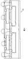
图1是为根据本发明的具有堆栈芯片的半导体组件封装的剖面图;1 is a cross-sectional view of a semiconductor package with stacked chips according to the present invention;
图2是为根据本发明的具有堆栈芯片以及多个锡球的半导体组件封装的剖面图;2 is a cross-sectional view of a semiconductor component package with stacked chips and a plurality of solder balls according to the present invention;
图3是为根据本发明的一实施例的具有并排结构的半导体组件封装的剖面图;3 is a cross-sectional view of a semiconductor device package with a side-by-side structure according to an embodiment of the present invention;
图4是为根据本发明的另一实施例的具有并排以及堆栈结构的半导体组件封装的剖面图;4 is a cross-sectional view of semiconductor device packages with side-by-side and stacked structures according to another embodiment of the present invention;
图5(a)是为根据本发明的半导体组件多晶封装的一实施例的剖面图;FIG. 5(a) is a cross-sectional view of an embodiment of a semiconductor component polycrystalline package according to the present invention;
图5(b)是为根据本发明的具有一预形成的晶粒容纳凹槽的衬底的半导体组件多晶封装的剖面图;FIG. 5( b) is a cross-sectional view of a semiconductor device polycrystalline package with a substrate having a pre-formed die receiving groove according to the present invention;
图6(a)至图6(c)是为根据本发明的衬底以及工具的组合的剖面图;Fig. 6 (a) to Fig. 6 (c) are the cross-sectional views for the combination of substrate and tool according to the present invention;
图7是为根据本发明的衬底以及工具的组合的俯视图;Figure 7 is a top view of a combination of a substrate and a tool according to the present invention;
图8是为根据本发明的粘贴于印刷电路板或母板的多晶封装的组合的剖面图。8 is a cross-sectional view of an assembly of polycrystalline packages attached to a printed circuit board or motherboard according to the present invention.
主要组件符号说明Explanation of main component symbols
100:半导体组件封装100: Semiconductor component packaging
102:衬底102: Substrate
104:第一晶粒104: First Die
105:晶粒容纳凹槽105: Die receiving groove
106:第一晶粒粘着材料106: First Die Attach Material
108:输入/输出垫108: Input/Output Pad
110:第一介电层110: first dielectric layer
112:端点金属接垫112: Terminal metal pad
114:第一重布层114: First redistribution layer
116:第二介电层116: second dielectric layer
118:第二晶粒粘着材料118: Second Die Adhesive Material
120:第二晶粒120: second grain
122:连接垫122: connection pad
124:粘合膏124: adhesive paste
126:通孔126: Through hole
128:第二重布层128: Second redistribution layer
130:第三介电层130: third dielectric layer
132:端点垫132: Endpoint Pad
134:覆盖层134: Overlay
136:切割道136: Cutting Road
138:焊锡凸块138: Solder bump
300:并排结构300: side-by-side structure
400:堆栈结构400: stack structure
600:周围区域600: surrounding area
602:玻璃载具602: Glass Vehicle
604:粘着材料604: Adhesive material
800:印刷电路板封装800: Printed Circuit Board Package
804:硅晶粒804: silicon grain
810:介电层810: dielectric layer
814:重布层金属814: Redistributed layer metal
824:间隙824: gap
832:球下金属层832: metal layer under the ball
838:晶粒垫838: Die Pad
840:印刷电路板840: Printed Circuit Board
842:金属垫842: metal pad
具体实施方式Detailed ways
本发明揭露了一种半导体组件封装结构,此组件利用了一具有业已定义端点金属接垫形成于其上的衬底且此衬底中具有一预设的凹槽。一晶粒是由粘着而配置于晶粒容纳凹槽之内。一感光材料(photosensitivematerial)是涂布于上述晶粒以及预形成的衬底上。较佳的情况下,上述感光材料是由弹性材料所形成。The invention discloses a packaging structure of a semiconductor component. The component utilizes a substrate with defined terminal metal pads formed thereon and a predetermined groove in the substrate. A die is disposed in the die receiving groove by adhesion. A photosensitive material is coated on the die and the preformed substrate. Preferably, the photosensitive material is made of elastic material.
参考图1,其是为根据本发明的半导体组件封装的剖面图。此半导体组件封装100包含:一衬底102;一第一晶粒104;一第二晶粒120;一晶粒容纳凹槽105;一第一晶粒粘着材料106;一第二晶粒粘着材料118;一第一介电层110、一第二介电层116及一第三介电层130;粘合膏124;一通孔126;一第一重布层114;一第二重布层128;一覆盖层134;端点垫132;及多个锡球138。Referring to FIG. 1 , it is a cross-sectional view of a semiconductor device package according to the present invention. The
在图1中,衬底102具有一预形成于衬底102的上表面内的晶粒容纳凹槽105,用以配置一第一晶粒104。一覆盖层134是形成于衬底102的下表面上,以便于制作激光标记(laser mark)或加以保护。覆盖层134的材料包含了环氧化物。In FIG. 1 , the
第一晶粒104是配置于衬底102上的晶粒容纳凹槽105内,并由第一晶粒粘着材料106(弹性材料为较佳)而固定。如了解,多个连接垫108是形成于第一晶粒104的上表面内。一第一介电层110是形成于第一晶粒104之上并填满于第一晶粒104以及晶粒容纳凹槽105的侧壁间的间隙。多个开口是由光刻制程(lithography process)或曝光与显影步骤(exposure and develop procedure)形成于第一介电层110之内。上述多个开口是分别与连接垫或输入/输出垫108以及端点金属接垫112对准的。The
第一重布层114,亦称为导电布线(conductive trace)114,是由选择性的移除形成于第一介电层110上的所特定的部分金属层(晶种层,seed layer)而形成于第一介电层110之上,其中第一重布层114是通过输入/输出垫108以及端点金属接垫112而与第一晶粒104保持电性连接。第一重布层114的部分材料将填满第一介电层110内的开口。接着,第二介电层116是形成于第一介电层110以及第一重布层114之上,换言之,第二介电层116是填入第一重布层114间的空间。The
在将一第二晶粒粘着层118约略对准第一晶粒104并粘贴至第二介电层116之上后,一第二晶粒120是配置于第二介电层116之上,上述晶粒粘着层118以及第二介电层116可为相同材料。如了解,多个连接垫122是形成于第二晶粒120的上表面内。粘合膏124是形成于第二晶粒120之上并填入第二晶粒120下表面下除第二晶粒粘着材料118以外的间隙。多个开口是由光刻制程或曝光与显影步骤或激光钻孔制程(laser drill process)形成并对准连接垫或输入/输出垫122。需注意的是,粘合膏124另外具有一通孔126形成于其上,可用与第一重布层114保持连接。一第二重布层128是形成于粘合膏124之上并填入通孔126之内以耦合至第一重布层114。换句话说,第一重布层114以及第二重布层128可由第二重布层128而填满通孔126并与对方保持电性连接。第一重布层114以及第二重布层128是分别耦合至第一晶粒104以及第二晶粒120,而第一晶粒104以及第二晶粒120是由通孔126与第一重布层114以及第二重布层128保持连接。After approximately aligning a second die attach
一第三介电层130是形成于第二重布层128以及粘合膏124之上,并有多个开口形成于第二重布层128之上。端点垫132是位于第三介电层130之上且连接至第二重布层128,并连接至第一重布层114以及衬底102的端点金属接垫112。每封装单元100间会定义为一切割道(scribe line)136,以便于每个单元的切割。A
在一实施例中,第一介电层110、第二介电层116以及第三介电层130包含一弹性介电层、一感光层(photosensitive layer)、一硅介电层、一硅氧烷聚合物(SINR)层、一聚亚酰胺(polyimide,PI)层或硅树脂(silicone resin)层。较佳的材料为包含硅氧烷聚合物(SINR)、Dow Corning WL 5000是列及其合成物的硅介电材料所做成的弹性介电材料。在另一实施例中,第一介电层110、第二介电层116及第三介电层130是由包含聚亚酰胺(PI)或硅树脂的材料所做成的。在较佳的情况下,其是一感光层以利于制程的简化。In one embodiment, the
在一实施例中,第一重布层114及第二重布层128的材料是为一包含钛/铜/金合金(Ti/Cu/Au alloy)或钛/铜/镍/金合金(Ti/Cu/Ni/Aualloy)的合金。另外,一晶种金属层(seed metal layer)(未显示于图中)是溅镀于第一重布层114及第二重布层128中(形成重布层的一部分)。In one embodiment, the material of the
第一介电层110是形成于第一晶粒104以及衬底102之上并填满环绕于第一晶粒周围的空间;由于第一介电层具有弹性特质,故可作为缓冲区以吸收于温度循环中介于第一晶粒104及衬底102间的热机械应力。前述的堆栈结构构成基板栅格阵列(Land Grid Array,LGA)型的封装。图2显示出另一可行的实施例,导电球体或焊锡凸块138是形成于端点垫132上。此方式是为球门阵列型(Ball Grid Array,BGA)的封装。由于其它部分与图1相似,因此省略详细叙述。在球门阵列(BGA)结构下,端点垫132是作为焊锡凸块138下的球下金属层(under ballmetal,UBM)。多个端点导电接垫132是形成于第二重布层128之上。The
较佳的情况下,衬底102的材料是为有机衬底例如FR4、FR5、BT(Bismaleimide triazine)、具有已定义凹槽(defined cavity)的印刷电路板(PCB)或具有预蚀刻电路(pre etching circuit)的Alloy 42。较佳的情况下,具有高玻璃转移温度的有机衬底是为环氧化物型的FR 5或BT型衬底。衬底102的材料也可为金属、合金、玻璃、硅、陶瓷。Alloy42是由42%镍以及58%铁所组成。也可使用Kovar,其成分为29%镍、17%钴以及54%铁。玻璃、陶瓷、硅亦可做为衬底。须注意的是,上述材料仅为描述本发明而非用以限制本发明。Preferably, the material of the
环氧化物型有机衬底(FR 5/BT)的热膨胀系数(X/Y方向)约为16而采用玻璃材料所制成的晶粒重布工具(die redistribution tool)则约为5至8。但是,当采用FR 5/BT材料所制成的晶粒重布工具时,由于衬底与晶粒重布工具的热膨胀系数为一致的,故不需要考虑晶粒移位的问题。由于晶圆级封装制程需经历数个高温制程,而FR 5/BT型衬底无法于温度循环后(接近玻璃转移温度)回归其原始位置,故会造成面板型(panelform)衬底上晶粒的移位。举例来说,当使用玻璃材料所制成的重布工具时,在形成介电层、热固晶粒粘着材料等步骤后必须确保有机衬底可保持在原始位置并确认制程中没有产生任何翘曲的问题。The thermal expansion coefficient (X/Y direction) of the epoxy-type organic substrate (
请参考图3,其是根据本发明的一实施例的具有并排结构(side-by-side structure)的半导体组件封装的剖面图。本发明进一歩提供了一具有多个个并排晶粒的并排结构300。Please refer to FIG. 3 , which is a cross-sectional view of a semiconductor device package with a side-by-side structure according to an embodiment of the present invention. The present invention further provides a side-by-
参照图4,其是根据本发明的另一实施例的具有并排以及堆栈结构的半导体组件封装的剖面图。本发明也提供了一具有多个个并排且互相堆栈的晶粒的并排及堆栈结构400。Referring to FIG. 4 , it is a cross-sectional view of semiconductor device packages with side-by-side and stacked structures according to another embodiment of the present invention. The present invention also provides a side-by-side and stack
如图5(a)所示,衬底102可为圆型(round type),例如晶圆型(wafer type),其直径(diameter)可为200、300mm或更高。也可以采用矩型(rectangular type),例如面板型。图5(a)为面板型衬底102于制程结束后,未切割为个别晶粒前的图示。如图所示,衬底102及位于其上的晶粒容纳凹槽105是预形成的。在图5(a)中,图1的封装单元是排列成矩阵型(matrix form)。参照图5(b),其显示出一具有一预形成的晶粒容纳凹槽105的衬底102的半导体组件封装,而覆盖层134是形成于衬底102的下表面上。As shown in FIG. 5( a ), the
请参照图6(a),由图中可看出衬底102的周围(边缘)区域600未有任何晶粒容纳凹槽形成。一晶粒重布工具602,例如玻璃载具,具有粘着材料(较佳的为UV固化型)604形成于玻璃工具602的周围区域600,用以在晶圆级封装制程中处理(粘贴)有机衬底102,如图6(b)所示。图6(c)为真空连接(vacuum bonding)及UV固化后,玻璃载具602以及衬底102的组合。Referring to FIG. 6( a ), it can be seen from the figure that no die receiving grooves are formed in the peripheral (edge)
参照图7,其显示出衬底102的边缘区域不包含晶粒容纳凹槽105,而在晶圆级封装制程中,周围区域600将用以粘贴玻璃载具602(其中载具的材料可为玻璃、硅、陶瓷、印刷电路板及Alloy 42等与晶粒重布工具的热膨胀系数相符的材料,为了克服由高温固化所产生的晶粒移位问题,衬底以及晶粒重布工具的材料是以相同材料为佳)。衬底102将与玻璃载具602粘接,并将于制程中固定及托住衬底102。在晶圆级封装制程结束后,由虚线所显示出的区域600将由玻璃载具602切除,而由虚线所定义的内部区域将执行切割制程(sawing process),以便于封装切割(package singulation)。Referring to FIG. 7, it shows that the edge region of the
在本发明的一实施例中,上述弹性介电层是为一种热膨胀系数大于100(ppm/℃)、延伸速率(elongation rate)约40%(较佳的为30%至50%)及硬度(hardness)介于塑料与橡胶间的材料。弹性介电层的厚度是依照温度循环试验(temperature cycling test)期间重布层/介电层界面中所累积的应力(stress)而决定。In one embodiment of the present invention, the above-mentioned elastic dielectric layer is a material with a thermal expansion coefficient greater than 100 (ppm/°C), an elongation rate (elongation rate) of about 40% (preferably 30% to 50%), and a hardness (Hardness) A material between plastic and rubber. The thickness of the elastic dielectric layer is determined according to the stress accumulated in the RDL/dielectric layer interface during a temperature cycling test.
图8显示出粘贴于印刷电路板或母板840的封装800的组合的剖面图。在图8中,其显示出与热膨胀系数问题相关的主要部分。硅晶粒804(热膨胀系数为2.3)是封装于一封装结构的中。衬底802是采用FR 5或BT有机环氧型材料(热膨胀系数约为16),而其热膨胀系数是与印刷电路板或母版840相同。晶粒804以及衬底802的间隙824是填满弹性材料,用以吸收(介于晶粒以及FR 5/BT衬底间)热膨胀系数不相符时所产生的热机械应力。另外,介电层810包含用以吸收晶粒垫838以及印刷电路板840间的应力的弹性材料。重布层金属814是铜/金的材料,而其热膨胀系数是与印刷电路板840以及有机衬底802相同,皆约为16,而接触凸块(contact bump)的球下金属层832是位于衬底802的端点金属接垫上。印刷电路板的金属垫842是由铜所制成,而其热膨胀系数是与印刷电路板840相同,皆大约为16。由上述叙述可发现,本发明可提供解决扩散式晶圆级封装(Fan-out WLP)的热膨胀系数问题的方案。FIG. 8 shows a cross-sectional view of the assembly of the
显然的,本发明的结构可解决堆栈增层(built-up layers)(印刷电路板以及衬底)下的热膨胀系数相符的问题,并提供更加的可靠度(板上不会产生X/Y方向的热应力),以及采用弹性介电层来吸收Z方向的应力。切割步骤中只需考虑到衬底材料(环氧化物型)的影响。芯片边缘以及凹槽侧壁的间隙824可填满弹性介电材料用以吸收机械/热应力。Obviously, the structure of the present invention can solve the problem that the thermal expansion coefficients under the stacked built-up layers (printed circuit board and substrate) are consistent, and provide more reliability (X/Y direction will not be generated on the board) thermal stress), and an elastic dielectric layer is used to absorb the stress in the Z direction. Only the influence of the substrate material (epoxy type) needs to be considered in the dicing step. The
在一实施例中,第一重布层114以及第二重布层128的厚度是介于2μm以及15μm之间。钛/铜合金(Ti/Cu alloy)是利用溅镀(sputtering)技术所形成,例如晶种金属层,而铜/金或铜/镍/金合金(Cu/Ni/Au alloy)是由电镀(electroplating)技术所形成,利用电镀制程形成第一重布层114及第二重布层128可使第一114及第二重布层128具有足够的厚度以容忍温度循环期间的热膨胀系数不相符。金属垫可为铝或铜或其组合。如果半导体组件的结构是利用硅氧烷聚合物(SINR)为弹性介电层而铜为重布层,则根据未显示于本说明书的应力分析,累积于重布层/介电层界面中的应力是降低了。In one embodiment, the thickness of the
如图1至图5(a)所示,第一重布层114以及第二重布层128是分别由第一晶粒104以及第二晶粒120扇出(fans out)(扩散),并由通孔126互相耦合以与端点垫132连接。其不同于先前技术之处在于,上述第一晶粒104是配置于衬底102的预形成的凹槽105内,从而减低封装的厚度。上述先前技术违反了减低晶粒封装厚度的原则。本发明的封装将较先前技术为薄。再者,衬底102是于封装前预先制备,且晶粒容纳凹槽105是于封装前预先形成。因此,产能(throughput)可较以往更为增进。本发明揭露一种具有低厚度以及良好热膨胀系数效能(good CTE performance)的扩散式晶圆级封装技术。As shown in FIG. 1 to FIG. 5(a), the
根据本发明的观点,本发明进一歩提供了一种形成一半导体组件多晶封装的方法。其所需的步骤是如下所述。According to the viewpoint of the present invention, the present invention further provides a method for forming a polycrystalline package of a semiconductor device. The steps required for this are described below.
本发明是提供一衬底102,衬底102具有一预形成于其上表面内的晶粒容纳凹槽105以及端点接垫112。接着,利用一拣选配置精细对准系统重新分布至少第一晶粒104于一具有所需间距的晶粒重布工具(未显示)上(上述晶粒重布工具具有对准图形以及用以粘贴第一晶粒104的主动面的图形胶)。载具602包含了位于载具602周围区域600的粘着材料604,用以粘接衬底102。接着,印刷粘着材料106于第一晶粒104的背面。具有载具602的衬底102是连接于第一晶粒104的背面上并真空固化(vacuum cured),而后,将晶粒重布工具由具有第一晶粒104以及载具602的衬底102分离。一第一介电层110是涂布于第一晶粒104以及衬底102上,并于后实行真空程序。一第一重布层114是形成于第一介电层110之上并耦合至第一晶粒104。而一第二介电层116则形成于其上,用以覆盖第一重布层114以及第一介电层110。The present invention provides a
接下来,至少第二晶粒120是配置于第二介电层116之上并由具有通孔126的粘合膏124覆盖于其上。形成一第二重布层128以耦合至第二晶粒120并填满通孔126以与第一重布层114形成电性连接。一第三介电层130是形成于第二重布层128之上。第一晶粒104以及第二晶粒120分别具有多个接垫108以及多个接垫122耦合至第一重布层114以及第二重布层128以由通孔126而互相达成电性连接。之后,多个锡球(soldering balls)138是焊接于第二重布层128之上。Next, at least the
在形成第一重布层114之前,一晶种金属层(未显示)是溅镀于第一介电层110、金属接垫112以及连接垫108的表面上。同样的,在形成第二重布层128之前,一晶种金属层也是溅镀于通孔126的内表面以及粘合膏124与连接垫122的表面上。上述晶种金属层的材料包含钛/铜。接着,于晶种金属层上涂布光阻层(photo resist layer)(未显示),并于光阻层盖上掩膜(photo masking),以形成第一重布层114以及第二重布层128。一铜/金或铜/镍/金薄膜(film)是电镀于封装的表面上。然后,剥离上述光阻层并由一种湿式蚀刻法(wet etchingmethod)移除上述晶种金属层,以形成封装表面上的重布层。Before forming the
须注意的是,上述所提及的结构的材料以及排列仅为描述而非用以限定本发明。根据不同导电的需求,上述结构的材料以及排列可依需求而加以更动。It should be noted that the materials and arrangement of the structures mentioned above are only for description but not for limiting the present invention. According to different conduction requirements, the materials and arrangements of the above structures can be changed according to requirements.
本发明的制程包含了提供一具有对准图形形成于其上的晶粒重布工具。接着,在印刷图形胶于上述工具上×用以粘贴晶粒的表面)后,利用具有覆晶功能×flip chip function)的拣选配置精细对准系统重新分布已知的好晶粒×即通过测试的晶粒)于一具有所需间距的晶粒重布工具上。晶粒将由上述图形胶粘贴于工具上。接下来,第一晶粒粘着材料是印刷于第一晶粒的背面×以弹性材料为佳)。之后,利用面板连接器×panelbonder)连接上述衬底于晶粒的背面;除了晶粒配置凹槽之外,衬底的上表面是粘贴于图形胶上,接着进行真空固化并将面板晶圆(panel wafer)以及上述工具分离。The process of the present invention involves providing a die redistribution tool having alignment patterns formed thereon. Then, after printing graphic glue on the above tool (for pasting the surface of the die), use the picking configuration fine alignment system with flip chip function (flip chip function) to redistribute the known good die (that is, pass the test die) on a die redistribution tool with the desired pitch. The die will be attached to the tool by the above graphic glue. Next, the first die attach material is printed on the backside of the first die (preferably elastic material). After that, use the panel connector × panelbonder) to connect the above substrate to the back of the die; except for the die configuration groove, the upper surface of the substrate is pasted on the pattern glue, and then vacuum-cured and the panel wafer ( panel wafer) and the separation of the above tools.
另一可行的方法是采用具有精细对准的晶粒连接机(die bondermachine),分配第一晶粒粘着材料于衬底102的晶粒容纳凹槽105上方或者具有粘贴胶带(tape)于其背面的第一晶粒104。第一晶粒104是配置于衬底102的晶粒容纳凹槽105之上。第一晶粒粘着材料106是经由热固化(thermally cured)来确保第一晶粒104是粘贴于衬底102之上。Another possible method is to use a die bonder machine with fine alignment, dispense the first die attach material over the
在将晶粒重新分布于衬底之上后,接着执行由湿式(wet)及/或干式清洗(dry clean)而清理晶粒表面的清理步骤。下一歩是将第一介电材料涂布于面板上,接着执行真空步骤以确保面板内没有气泡产生。接下来,执行光刻蚀刻制程以形成连接通孔部位(via)(金属接垫)、铝连接垫及/或切割道(选择性),或者也可实行激光钻孔制程。接着实行电桨清理步骤(plasma clean step),以清理铝连接垫及连接通孔的表面。下一步骤是溅镀钛/铜以作为晶种金属层,并将光阻涂布于介电层及晶种金属层之上,以利于形成重布金属层(RDL)的图案。接着,进行电镀制程形成铜/金或铜/镍/金以作为重布层金属,之后,剥离上述光阻并由湿式蚀刻步骤形成重布层金属布线(RDL metal trace)。而后,下一步骤是以涂布或印刷方式制作项介电层(top dielectric layer)并在其上形成接触凸块通孔(contact bump via)以产生球下金属层及/或形成切割线(选择性)。After redistribution of the die on the substrate, a cleaning step of cleaning the surface of the die by wet and/or dry clean is performed. The next step is to apply the first dielectric material on the panel, followed by a vacuum step to ensure that no air bubbles are generated inside the panel. Next, a photolithographic etching process is performed to form connection vias (metal pads), aluminum connection pads and/or dicing lines (optional), or a laser drilling process can also be performed. A plasma clean step is then performed to clean the surfaces of the aluminum connection pads and connection vias. The next step is to sputter Ti/Cu as a seed metal layer, and apply photoresist on top of the dielectric layer and the seed metal layer to facilitate patterning of the redistributed metal layer (RDL). Next, an electroplating process is performed to form copper/gold or copper/nickel/gold as the redistribution layer metal, and then the photoresist is stripped off and the RDL metal trace is formed by a wet etching step. Then, the next step is to make a top dielectric layer by coating or printing and form a contact bump via on it to produce an under-ball metal layer and/or form a dicing line ( optional).
在锡球配置或焊锡粘胶印刷之后,进行热回流制程(heat re-flowprocedure)以回流至衬底侧边(BGA型)。进行测试。面板晶圆级的最后测试是利用垂直式探针卡(vertical probe card)执行。在测试之后,衬底是经由切割以将上述封装分割成为个别单元。接着,将上述封装分别拣选及配置于托盘(tray)或胶膜(tape)及卷带(reel)等传输装置上。After solder ball placement or solder paste printing, a heat re-flow procedure is performed to reflow to the side of the substrate (BGA type). carry out testing. The final test at the wafer level of the panel is performed using a vertical probe card. After testing, the substrate is diced to separate the packages into individual units. Next, the above-mentioned packages are sorted and placed on transport devices such as trays, tapes, and reels, respectively.
根据本发明的观点,本发明的优点是如下所述。本发明的制程是为形成面板晶圆的简易方法,且容易在晶圆级制程中控制面板表面的粗糙度。在制程中,面板(晶粒附于其上)的厚度可容易控制且不会产生晶粒移位的问题。可免除注射模具的需求并可避免翘曲以及化学机械研磨制程(CMPprocess)。另外,具有预形成的晶粒容纳凹槽以及端点金属接垫(有机衬底)的衬底是预先制备的;晶粒容纳凹槽的尺寸等于晶粒的尺寸再于晶粒每一边加上大约50μm至100μm。其可填入弹性介电材料藉以吸收由硅晶粒与衬底(FR 5/BT)间的热膨胀系数不相符所产生的热应力,以作为应力缓冲释放区域。由于将简易增层应用于晶粒的上表面,故可增加封装产率(减少制造周期的时间)。端点垫是形成于晶粒主动面的同一表面上。From the viewpoint of the present invention, the advantages of the present invention are as follows. The manufacturing process of the present invention is a simple method for forming a panel wafer, and it is easy to control the roughness of the panel surface in the wafer-level manufacturing process. During the process, the thickness of the panel (on which the die is attached) can be easily controlled without the problem of die displacement. The need for injection molds can be eliminated and warpage and chemical mechanical polishing process (CMP process) can be avoided. In addition, the substrate with pre-formed die-receiving grooves and terminal metal pads (organic substrate) is pre-prepared; the size of the die-receiving groove is equal to the size of the die plus approximately 50μm to 100μm. It can be filled with elastic dielectric material to absorb the thermal stress caused by the thermal expansion coefficient mismatch between the silicon grain and the substrate (
此外,上述晶粒配置制程是与目前的制程相同。本发明不需要填入任何粘合膏(树脂、环氧化合物、硅橡胶等)。热膨胀系数不相符的问题是于面板形成制程中克服,而晶粒及衬底FR 4中间的深度只有约20μm至50μm(作为晶粒配置后的厚度),当晶粒配置于衬底的晶粒容纳凹槽之后,晶粒以及衬底的表面层级(surface level)将会是相同的。仅有硅介电材料(以硅材料的硅氧烷聚合物(SINR)为佳)是涂布于主动面以及衬底(以FR 5或BT为佳)的表面上。由于介电层(硅氧烷聚合物(SINR))是以感光层而形成接触开口(contacting open),故接垫是利用掩膜制程(photo mask process)而形成。为了避免于填满晶粒以及衬底的凹槽侧壁的间隙时产生气泡,涂布介电材料(硅氧烷聚合物(SINR)时是采用真空制程。在衬底与晶粒(芯片)连接之前,晶粒粘着材料是印刷于晶粒的背面。封装与基板层级的可靠度是较已知技术为佳,特别是在基板层级温度循环试验,由于衬底与印刷电路板母板的热膨胀系数完全相同,因此并无热机械应力提供至焊锡凸块/球;而基板测试的温度循环期间所造成的先前失效模式(previous failure mode)(如锡球碎裂(solder ballcrack))便较不易发生。因此可降低成本及简化制程。亦易于形成多重晶粒的封装。In addition, the above-mentioned die allocation process is the same as the current process. The present invention does not require any adhesive paste (resin, epoxy, silicone rubber, etc.) to be filled. The problem of inconsistent thermal expansion coefficients is overcome in the panel formation process, and the depth between the die and the substrate FR 4 is only about 20 μm to 50 μm (as the thickness after the die is arranged), when the die is arranged on the die of the substrate After accommodating the grooves, the surface level of the die and substrate will be the same. Only the silicon dielectric material (preferably siloxane polymer of silicon material (SINR)) is coated on the active surface and the surface of the substrate (preferably
根据上述,本发明所揭露的半导体组件多晶封装结构及其方法可提供先前技术所无法预期的效果,并解决先前技术的问题。需注意的是,本发明可应用于晶圆或面板(LCD显示器,印刷电路板/衬底)产业,并可修改及应用于其它方面上。According to the above, the semiconductor device polycrystalline packaging structure and method disclosed in the present invention can provide unexpected effects and solve the problems of the prior art. It should be noted that the present invention can be applied to the wafer or panel (LCD display, printed circuit board/substrate) industry, and can be modified and applied to other aspects.
本发明以较佳实施例说明如上,然其并非用以限定本发明所主张的专利权利范围。其专利保护范围当视本发明所附的权利要求范围及其等同领域而定。凡熟悉此领域的技术者,在不脱离本专利精神或范围内,所作的更动或润饰,均属于本发明所揭示精神下所完成的等效改变或设计,且应包含在本发明的权利要求范围内。The present invention is described above with preferred embodiments, but it is not intended to limit the scope of patent rights claimed by the present invention. The scope of its patent protection shall be determined by the scope of the appended claims of the present invention and their equivalent fields. Any changes or modifications made by those skilled in the art without departing from the spirit or scope of this patent belong to the equivalent changes or designs completed under the spirit disclosed by the present invention, and shall be included in the rights of the present invention. within the required range.
Claims (10)
Translated fromChineseApplications Claiming Priority (2)
| Application Number | Priority Date | Filing Date | Title |
|---|---|---|---|
| US11/715,358US20080217761A1 (en) | 2007-03-08 | 2007-03-08 | Structure of semiconductor device package and method of the same |
| US11/715,358 | 2007-03-08 |
Publications (1)
| Publication Number | Publication Date |
|---|---|
| CN101261984Atrue CN101261984A (en) | 2008-09-10 |
Family
ID=39740819
Family Applications (1)
| Application Number | Title | Priority Date | Filing Date |
|---|---|---|---|
| CNA200810083485XAPendingCN101261984A (en) | 2007-03-08 | 2008-03-07 | Semiconductor assembly packaging structure and method thereof |
Country Status (7)
| Country | Link |
|---|---|
| US (1) | US20080217761A1 (en) |
| JP (1) | JP2008252087A (en) |
| KR (1) | KR20080082545A (en) |
| CN (1) | CN101261984A (en) |
| DE (1) | DE102008013180A1 (en) |
| SG (1) | SG145683A1 (en) |
| TW (1) | TW200908249A (en) |
Cited By (33)
| Publication number | Priority date | Publication date | Assignee | Title |
|---|---|---|---|---|
| CN101924041A (en)* | 2009-06-16 | 2010-12-22 | 飞思卡尔半导体公司 | Method for assembling stackable semiconductor packaging |
| CN102439719A (en)* | 2009-05-14 | 2012-05-02 | 米辑电子股份有限公司 | System-in packages |
| CN102709200A (en)* | 2011-01-21 | 2012-10-03 | 新科金朋有限公司 | Semiconductor device and method of forming insulating layer disposed over the semiconductor die for stress relief |
| CN103545288A (en)* | 2012-07-13 | 2014-01-29 | 英特尔移动通信有限责任公司 | Stacked fan-out semiconductor chips |
| CN103646881A (en)* | 2013-09-30 | 2014-03-19 | 南通富士通微电子股份有限公司 | Wafer packaging method |
| CN103985650A (en)* | 2014-06-03 | 2014-08-13 | 杭州大立微电子有限公司 | Encapsulation mold and encapsulation method |
| CN104051365A (en)* | 2013-03-14 | 2014-09-17 | 英特尔移动通信有限责任公司 | Chip arrangement and method for manufacturing chip arrangement |
| CN104795380A (en)* | 2015-03-27 | 2015-07-22 | 江阴长电先进封装有限公司 | Three-dimensional packaging structure |
| CN105261627A (en)* | 2015-10-19 | 2016-01-20 | 格科微电子(上海)有限公司 | CSP method and part of image sensor chip |
| US9252066B2 (en) | 2007-12-14 | 2016-02-02 | Stats Chippac, Ltd. | Semiconductor device and method of forming interconnect structure for encapsulated die having pre-applied protective layer |
| US9318441B2 (en) | 2007-12-14 | 2016-04-19 | Stats Chippac, Ltd. | Semiconductor device and method of forming sacrificial adhesive over contact pads of semiconductor die |
| US9472452B2 (en) | 2010-03-15 | 2016-10-18 | STATS ChipPAC Pte. Ltd. | Semiconductor device and method of forming repassivation layer with reduced opening to contact pad of semiconductor die |
| CN106057768A (en)* | 2015-04-17 | 2016-10-26 | 台湾积体电路制造股份有限公司 | Fan-out POP structure with inconsecutive polymer layer |
| US9536285B2 (en) | 2012-07-11 | 2017-01-03 | Tencent Technology (Shenzhen) Company Limited | Image processing method, client, and image processing system |
| US9558958B2 (en) | 2010-03-12 | 2017-01-31 | STATS ChipPAC Pte. Ltd. | Semiconductor device and method of forming sacrificial protective layer to protect semiconductor die edge during singulation |
| CN106653619A (en)* | 2015-10-30 | 2017-05-10 | 英飞凌科技股份有限公司 | Method for producing power semiconductor module |
| US9666500B2 (en) | 2007-12-14 | 2017-05-30 | STATS ChipPAC Pte. Ltd. | Semiconductor device and method of forming insulating layer disposed over the semiconductor die for stress relief |
| US9754867B2 (en) | 2010-03-15 | 2017-09-05 | STATS ChipPAC Pte. Ltd. | Semiconductor device and method of forming repassivation layer for robust low cost fan-out semiconductor package |
| CN107393836A (en)* | 2017-06-19 | 2017-11-24 | 矽力杰半导体技术(杭州)有限公司 | Chip packaging method and encapsulating structure |
| CN107564893A (en)* | 2016-06-30 | 2018-01-09 | 台湾积体电路制造股份有限公司 | Semiconductor structure and manufacturing method thereof |
| CN108400119A (en)* | 2017-02-08 | 2018-08-14 | 美光科技公司 | Semiconductor packages and its manufacturing method |
| CN109425810A (en)* | 2017-08-18 | 2019-03-05 | 台湾积体电路制造股份有限公司 | Semiconductor test apparatus, semiconductor test system, and semiconductor test method |
| CN109559998A (en)* | 2017-09-26 | 2019-04-02 | 新加坡商格罗方德半导体私人有限公司 | Magnetic screen encapsulating structure and its manufacturing method for MRAM device |
| CN109786348A (en)* | 2017-11-15 | 2019-05-21 | 台湾积体电路制造股份有限公司 | It is formed and has reeded metal joined article |
| CN109786362A (en)* | 2017-11-14 | 2019-05-21 | 旺宏电子股份有限公司 | Without weld pad exterior wing crystal grain laminated construction and preparation method thereof |
| CN110010479A (en)* | 2018-10-10 | 2019-07-12 | 浙江集迈科微电子有限公司 | A kind of Fan-out packaging technology of radio frequency chip |
| TWI675449B (en)* | 2017-11-30 | 2019-10-21 | 南韓商三星電子股份有限公司 | Semiconductor package |
| CN110828496A (en)* | 2019-11-15 | 2020-02-21 | 华天科技(昆山)电子有限公司 | Semiconductor device and method for manufacturing the same |
| CN111958078A (en)* | 2020-09-27 | 2020-11-20 | 淄博晨启电子有限公司 | Welding process of high-reliability high-surge impact capability semiconductor protection device |
| CN113078149A (en)* | 2021-03-12 | 2021-07-06 | 上海易卜半导体有限公司 | Semiconductor packaging structure, method, device and electronic product |
| CN113782509A (en)* | 2021-11-12 | 2021-12-10 | 深圳市时代速信科技有限公司 | Semiconductor device and preparation method thereof |
| CN116692765A (en)* | 2016-01-13 | 2023-09-05 | 德克萨斯仪器股份有限公司 | Structure and method for packaging stress sensitive MEMS |
| CN118070749A (en)* | 2024-04-17 | 2024-05-24 | 淄博芯材集成电路有限责任公司 | Substrate shrinkage method |
Families Citing this family (64)
| Publication number | Priority date | Publication date | Assignee | Title |
|---|---|---|---|---|
| US20080157398A1 (en)* | 2007-01-03 | 2008-07-03 | Advanced Chip Engineering Technology Inc. | Semiconductor device package having pseudo chips |
| US8049323B2 (en)* | 2007-02-16 | 2011-11-01 | Taiwan Semiconductor Manufacturing Co., Ltd. | Chip holder with wafer level redistribution layer |
| US7994622B2 (en) | 2007-04-16 | 2011-08-09 | Tessera, Inc. | Microelectronic packages having cavities for receiving microelectric elements |
| US8536692B2 (en)* | 2007-12-12 | 2013-09-17 | Stats Chippac Ltd. | Mountable integrated circuit package system with mountable integrated circuit die |
| US20090243069A1 (en)* | 2008-03-26 | 2009-10-01 | Zigmund Ramirez Camacho | Integrated circuit package system with redistribution |
| US9293385B2 (en)* | 2008-07-30 | 2016-03-22 | Stats Chippac Ltd. | RDL patterning with package on package system |
| US8350377B2 (en)* | 2008-09-25 | 2013-01-08 | Wen-Kun Yang | Semiconductor device package structure and method for the same |
| US8232633B2 (en)* | 2008-09-25 | 2012-07-31 | King Dragon International Inc. | Image sensor package with dual substrates and the method of the same |
| KR101003678B1 (en)* | 2008-12-03 | 2010-12-23 | 삼성전기주식회사 | wafer level package and method of manufacturing the same and method for reusing chip |
| TWM362572U (en)* | 2009-04-13 | 2009-08-01 | Phytrex Technology Corp | Signal convertor |
| TWI455215B (en)* | 2009-06-11 | 2014-10-01 | Advanced Semiconductor Eng | Semiconductor package and manufacturing method thereof |
| US8518749B2 (en) | 2009-06-22 | 2013-08-27 | Stats Chippac, Ltd. | Semiconductor device and method of forming prefabricated heat spreader frame with embedded semiconductor die |
| TWI421992B (en)* | 2009-08-05 | 2014-01-01 | Unimicron Technology Corp | Package substrate and fabrication method thereof |
| TWI528514B (en)* | 2009-08-20 | 2016-04-01 | 精材科技股份有限公司 | Chip package and fabrication method thereof |
| US8476750B2 (en)* | 2009-12-10 | 2013-07-02 | Qualcomm Incorporated | Printed circuit board having embedded dies and method of forming same |
| US20110147910A1 (en)* | 2009-12-21 | 2011-06-23 | Micron Technology, Inc. | Method for stacking die in thin, small-outline package |
| FR2960095A1 (en)* | 2010-05-17 | 2011-11-18 | St Microelectronics Grenoble 2 | METHOD FOR MANUFACTURING SEMICONDUCTOR DEVICES AND SEMICONDUCTOR DEVICE COMPRISING A THROUGH VIAS CHIP |
| US8528827B2 (en)* | 2010-06-18 | 2013-09-10 | Semiconductor Energy Laboratory Co., Ltd. | Antenna, semiconductor device, and method of manufacturing antenna |
| US8492911B2 (en)* | 2010-07-20 | 2013-07-23 | Lsi Corporation | Stacked interconnect heat sink |
| JP5703010B2 (en) | 2010-12-16 | 2015-04-15 | 新光電気工業株式会社 | Semiconductor package and manufacturing method thereof |
| US8736065B2 (en)* | 2010-12-22 | 2014-05-27 | Intel Corporation | Multi-chip package having a substrate with a plurality of vertically embedded die and a process of forming the same |
| US8647796B2 (en)* | 2011-07-27 | 2014-02-11 | Taiwan Semiconductor Manufacturing Company, Ltd. | Photoactive compound gradient photoresist |
| KR102020001B1 (en) | 2011-10-21 | 2019-09-09 | 루미리즈 홀딩 비.브이. | Low warpage wafer bonding through use of slotted substrates |
| US9508674B2 (en)* | 2012-11-14 | 2016-11-29 | Taiwan Semiconductor Manufacturing Company, Ltd. | Warpage control of semiconductor die package |
| TWI540768B (en)* | 2012-12-21 | 2016-07-01 | 鴻海精密工業股份有限公司 | Light-emitting chip combination and manufacturing method thereof |
| US9236368B2 (en)* | 2013-01-28 | 2016-01-12 | Sandisk Information Technology (Shanghai) Co., Ltd. | Semiconductor device including embedded controller die and method of making same |
| US8912663B1 (en)* | 2013-06-28 | 2014-12-16 | Delta Electronics, Inc. | Embedded package structure and method for manufacturing thereof |
| KR102088531B1 (en)* | 2013-11-25 | 2020-03-12 | 에스케이하이닉스 주식회사 | Thin embedded package and method of fabricating the same |
| EP2947692B1 (en)* | 2013-12-20 | 2020-09-23 | Analog Devices, Inc. | Integrated device die and package with stress reduction features |
| CN104793026B (en)* | 2014-01-20 | 2018-09-28 | 旺矽科技股份有限公司 | Supporting structure applied to probe testing device and manufacturing method thereof |
| KR20150144416A (en)* | 2014-06-16 | 2015-12-28 | 한국전자통신연구원 | Stack module package and method for manufacturing of the same |
| DE102014008838B4 (en) | 2014-06-20 | 2021-09-30 | Kunststoff-Zentrum In Leipzig Gemeinnützige Gmbh | Stress-reducing flexible connecting element for a microelectronic system |
| DE102014008839B4 (en) | 2014-06-20 | 2021-09-30 | Kunststoff-Zentrum In Leipzig Gemeinnützige Gmbh | Expansion-compensating connecting element for a microelectronic system |
| US9589915B2 (en)* | 2014-07-17 | 2017-03-07 | Taiwan Semiconductor Manufacturing Company Ltd. | Semiconductor device and manufacturing method thereof |
| TWI581387B (en) | 2014-09-11 | 2017-05-01 | 矽品精密工業股份有限公司 | Package structure and method of manufacture |
| US20160240457A1 (en)* | 2015-02-18 | 2016-08-18 | Altera Corporation | Integrated circuit packages with dual-sided stacking structure |
| US10287161B2 (en) | 2015-07-23 | 2019-05-14 | Analog Devices, Inc. | Stress isolation features for stacked dies |
| TWI634629B (en)* | 2015-08-20 | 2018-09-01 | 矽品精密工業股份有限公司 | Electronic package and method of manufacture thereof |
| KR102549402B1 (en) | 2016-08-04 | 2023-06-28 | 삼성전자주식회사 | Semiconductor package and method for fabricating the same |
| US20180166419A1 (en)* | 2016-12-12 | 2018-06-14 | Nanya Technology Corporation | Semiconductor package |
| US10529671B2 (en) | 2016-12-13 | 2020-01-07 | Taiwan Semiconductor Manufacturing Co., Ltd. | Package structure and method for forming the same |
| US20180166356A1 (en)* | 2016-12-13 | 2018-06-14 | Globalfoundries Inc. | Fan-out circuit packaging with integrated lid |
| US20180374717A1 (en)* | 2017-06-23 | 2018-12-27 | Powertech Technology Inc. | Semiconductor package and method of forming the same |
| US10665522B2 (en) | 2017-12-22 | 2020-05-26 | Intel IP Corporation | Package including an integrated routing layer and a molded routing layer |
| US11127716B2 (en) | 2018-04-12 | 2021-09-21 | Analog Devices International Unlimited Company | Mounting structures for integrated device packages |
| KR102081088B1 (en)* | 2018-08-29 | 2020-02-25 | 삼성전자주식회사 | Semiconductor package |
| EP3916770A4 (en) | 2019-03-07 | 2022-11-02 | Absolics Inc. | PACKAGING SUBSTRATE AND SEMICONDUCTOR DEVICE WITH IT |
| JP7293360B2 (en) | 2019-03-07 | 2023-06-19 | アブソリックス インコーポレイテッド | Packaging substrate and semiconductor device including the same |
| CN113261093B (en) | 2019-03-12 | 2024-04-16 | 爱玻索立克公司 | Semiconductor packaging substrate and method for preparing the same, and semiconductor device |
| KR102537005B1 (en) | 2019-03-12 | 2023-05-26 | 앱솔릭스 인코포레이티드 | Loading cassette for substrates containing glass and method for loading substrates using the same |
| WO2020185021A1 (en) | 2019-03-12 | 2020-09-17 | 에스케이씨 주식회사 | Packaging substrate, and semiconductor device comprising same |
| CN115440697B (en) | 2019-03-12 | 2025-08-15 | 爱玻索立克公司 | Package substrate and semiconductor device including the same |
| KR102515304B1 (en) | 2019-03-29 | 2023-03-29 | 앱솔릭스 인코포레이티드 | Packaging glass substrate for semiconductor, packaging substrate for semiconductor, and semiconductor device |
| US11380620B2 (en) | 2019-06-14 | 2022-07-05 | Taiwan Semiconductor Manufacturing Company, Ltd. | Semiconductor package including cavity-mounted device |
| KR102798702B1 (en)* | 2019-07-22 | 2025-04-23 | 삼성전자주식회사 | Semiconductor package |
| KR102413117B1 (en) | 2019-08-23 | 2022-06-24 | 앱솔릭스 인코포레이티드 | Packaging substrate and semiconductor device including same |
| US11462509B2 (en)* | 2019-10-29 | 2022-10-04 | Taiwan Semiconductor Manufacturing Co., Ltd. | Package structure with electronic device in cavity substrate and method for forming the same |
| DE102020200817B3 (en)* | 2020-01-23 | 2021-06-17 | Lpkf Laser & Electronics Aktiengesellschaft | Mounting method for an integrated semiconductor wafer device and mounting device usable therefor |
| TWI747261B (en)* | 2020-04-29 | 2021-11-21 | 典琦科技股份有限公司 | Method for manufacturing die package |
| US11664340B2 (en) | 2020-07-13 | 2023-05-30 | Analog Devices, Inc. | Negative fillet for mounting an integrated device die to a carrier |
| TWI756000B (en)* | 2020-12-28 | 2022-02-21 | 欣興電子股份有限公司 | Chip package structure and manufacturing method thereof |
| CN113471160A (en)* | 2021-06-29 | 2021-10-01 | 矽磐微电子(重庆)有限公司 | Chip packaging structure and manufacturing method thereof |
| DE102021119190A1 (en)* | 2021-07-23 | 2023-01-26 | Infineon Technologies Ag | Method for producing a document structure and document structure |
| US11810895B2 (en)* | 2021-10-14 | 2023-11-07 | Honeywell Federal Manufacturing & Technologies, Llc | Electrical interconnect structure using metal bridges to interconnect die |
Family Cites Families (1)
| Publication number | Priority date | Publication date | Assignee | Title |
|---|---|---|---|---|
| US7459781B2 (en) | 2003-12-03 | 2008-12-02 | Wen-Kun Yang | Fan out type wafer level package structure and method of the same |
- 2007
- 2007-03-08USUS11/715,358patent/US20080217761A1/ennot_activeAbandoned
- 2008
- 2008-03-06TWTW097107959Apatent/TW200908249A/enunknown
- 2008-03-07JPJP2008058397Apatent/JP2008252087A/ennot_activeWithdrawn
- 2008-03-07SGSG200801921-8Apatent/SG145683A1/enunknown
- 2008-03-07DEDE102008013180Apatent/DE102008013180A1/ennot_activeWithdrawn
- 2008-03-07CNCNA200810083485XApatent/CN101261984A/enactivePending
- 2008-03-10KRKR1020080021787Apatent/KR20080082545A/ennot_activeCeased
Cited By (52)
| Publication number | Priority date | Publication date | Assignee | Title |
|---|---|---|---|---|
| US9318441B2 (en) | 2007-12-14 | 2016-04-19 | Stats Chippac, Ltd. | Semiconductor device and method of forming sacrificial adhesive over contact pads of semiconductor die |
| US9252066B2 (en) | 2007-12-14 | 2016-02-02 | Stats Chippac, Ltd. | Semiconductor device and method of forming interconnect structure for encapsulated die having pre-applied protective layer |
| US9559029B2 (en) | 2007-12-14 | 2017-01-31 | STATS ChipPAC Pte. Ltd. | Semiconductor device and method of forming interconnect structure for encapsulated die having pre-applied protective layer |
| US10998248B2 (en) | 2007-12-14 | 2021-05-04 | JCET Semiconductor (Shaoxing) Co. Ltd. | Semiconductor device and method of forming sacrificial adhesive over contact pads of semiconductor die |
| US9666500B2 (en) | 2007-12-14 | 2017-05-30 | STATS ChipPAC Pte. Ltd. | Semiconductor device and method of forming insulating layer disposed over the semiconductor die for stress relief |
| CN102439719B (en)* | 2009-05-14 | 2015-06-24 | 高通股份有限公司 | System-in packages |
| CN102439719A (en)* | 2009-05-14 | 2012-05-02 | 米辑电子股份有限公司 | System-in packages |
| CN101924041A (en)* | 2009-06-16 | 2010-12-22 | 飞思卡尔半导体公司 | Method for assembling stackable semiconductor packaging |
| US9558958B2 (en) | 2010-03-12 | 2017-01-31 | STATS ChipPAC Pte. Ltd. | Semiconductor device and method of forming sacrificial protective layer to protect semiconductor die edge during singulation |
| US10204866B2 (en) | 2010-03-12 | 2019-02-12 | STATS ChipPAC Pte. Ltd. | Semiconductor device and method of forming sacrificial protective layer to protect semiconductor die edge during singulation |
| US9754867B2 (en) | 2010-03-15 | 2017-09-05 | STATS ChipPAC Pte. Ltd. | Semiconductor device and method of forming repassivation layer for robust low cost fan-out semiconductor package |
| US9472452B2 (en) | 2010-03-15 | 2016-10-18 | STATS ChipPAC Pte. Ltd. | Semiconductor device and method of forming repassivation layer with reduced opening to contact pad of semiconductor die |
| CN102709200A (en)* | 2011-01-21 | 2012-10-03 | 新科金朋有限公司 | Semiconductor device and method of forming insulating layer disposed over the semiconductor die for stress relief |
| CN102709200B (en)* | 2011-01-21 | 2016-08-03 | 新科金朋有限公司 | Semiconductor device and the method forming setting insulating barrier on a semiconductor die |
| US9536285B2 (en) | 2012-07-11 | 2017-01-03 | Tencent Technology (Shenzhen) Company Limited | Image processing method, client, and image processing system |
| CN103545288A (en)* | 2012-07-13 | 2014-01-29 | 英特尔移动通信有限责任公司 | Stacked fan-out semiconductor chips |
| CN104051365A (en)* | 2013-03-14 | 2014-09-17 | 英特尔移动通信有限责任公司 | Chip arrangement and method for manufacturing chip arrangement |
| CN103646881A (en)* | 2013-09-30 | 2014-03-19 | 南通富士通微电子股份有限公司 | Wafer packaging method |
| CN103985650B (en)* | 2014-06-03 | 2017-01-11 | 杭州大立微电子有限公司 | Encapsulation mold and encapsulation method |
| CN103985650A (en)* | 2014-06-03 | 2014-08-13 | 杭州大立微电子有限公司 | Encapsulation mold and encapsulation method |
| CN104795380A (en)* | 2015-03-27 | 2015-07-22 | 江阴长电先进封装有限公司 | Three-dimensional packaging structure |
| CN106057768A (en)* | 2015-04-17 | 2016-10-26 | 台湾积体电路制造股份有限公司 | Fan-out POP structure with inconsecutive polymer layer |
| CN106057768B (en)* | 2015-04-17 | 2019-06-11 | 台湾积体电路制造股份有限公司 | POP structure is fanned out to discontinuous polymeric layer |
| CN105261627A (en)* | 2015-10-19 | 2016-01-20 | 格科微电子(上海)有限公司 | CSP method and part of image sensor chip |
| CN106653619A (en)* | 2015-10-30 | 2017-05-10 | 英飞凌科技股份有限公司 | Method for producing power semiconductor module |
| CN116692765A (en)* | 2016-01-13 | 2023-09-05 | 德克萨斯仪器股份有限公司 | Structure and method for packaging stress sensitive MEMS |
| CN107564893A (en)* | 2016-06-30 | 2018-01-09 | 台湾积体电路制造股份有限公司 | Semiconductor structure and manufacturing method thereof |
| CN108400119A (en)* | 2017-02-08 | 2018-08-14 | 美光科技公司 | Semiconductor packages and its manufacturing method |
| CN108400119B (en)* | 2017-02-08 | 2020-07-31 | 美光科技公司 | Semiconductor package and method of manufacturing the same |
| US10629522B2 (en) | 2017-02-08 | 2020-04-21 | Micron Technology, Inc. | Semiconductor package and method for fabricating the same |
| CN107393836A (en)* | 2017-06-19 | 2017-11-24 | 矽力杰半导体技术(杭州)有限公司 | Chip packaging method and encapsulating structure |
| CN107393836B (en)* | 2017-06-19 | 2020-04-10 | 矽力杰半导体技术(杭州)有限公司 | Chip packaging method and packaging structure |
| CN109425810A (en)* | 2017-08-18 | 2019-03-05 | 台湾积体电路制造股份有限公司 | Semiconductor test apparatus, semiconductor test system, and semiconductor test method |
| CN109425810B (en)* | 2017-08-18 | 2021-08-24 | 台湾积体电路制造股份有限公司 | Semiconductor testing apparatus, semiconductor testing system, and semiconductor testing method |
| CN109559998A (en)* | 2017-09-26 | 2019-04-02 | 新加坡商格罗方德半导体私人有限公司 | Magnetic screen encapsulating structure and its manufacturing method for MRAM device |
| CN109559998B (en)* | 2017-09-26 | 2022-06-24 | 新加坡商格罗方德半导体私人有限公司 | Magnetic shielding package structure for MRAM device and method of manufacturing the same |
| CN109786362A (en)* | 2017-11-14 | 2019-05-21 | 旺宏电子股份有限公司 | Without weld pad exterior wing crystal grain laminated construction and preparation method thereof |
| CN109786348A (en)* | 2017-11-15 | 2019-05-21 | 台湾积体电路制造股份有限公司 | It is formed and has reeded metal joined article |
| US10685935B2 (en) | 2017-11-15 | 2020-06-16 | Taiwan Semiconductor Manufacturing Company, Ltd. | Forming metal bonds with recesses |
| US10854574B2 (en) | 2017-11-15 | 2020-12-01 | Taiwan Semiconductor Manufacturing Company, Ltd. | Forming metal bonds with recesses |
| CN109786348B (en)* | 2017-11-15 | 2021-03-16 | 台湾积体电路制造股份有限公司 | Metal joint with groove |
| TWI675449B (en)* | 2017-11-30 | 2019-10-21 | 南韓商三星電子股份有限公司 | Semiconductor package |
| CN110010479B (en)* | 2018-10-10 | 2021-04-06 | 浙江集迈科微电子有限公司 | Fan-out packaging process of radio frequency chip |
| CN110010479A (en)* | 2018-10-10 | 2019-07-12 | 浙江集迈科微电子有限公司 | A kind of Fan-out packaging technology of radio frequency chip |
| CN110828496A (en)* | 2019-11-15 | 2020-02-21 | 华天科技(昆山)电子有限公司 | Semiconductor device and method for manufacturing the same |
| CN111958078B (en)* | 2020-09-27 | 2021-08-27 | 淄博晨启电子有限公司 | Welding process of high-reliability high-surge impact capability semiconductor protection device |
| CN111958078A (en)* | 2020-09-27 | 2020-11-20 | 淄博晨启电子有限公司 | Welding process of high-reliability high-surge impact capability semiconductor protection device |
| CN113078149A (en)* | 2021-03-12 | 2021-07-06 | 上海易卜半导体有限公司 | Semiconductor packaging structure, method, device and electronic product |
| CN113078149B (en)* | 2021-03-12 | 2023-11-10 | 上海易卜半导体有限公司 | Semiconductor packaging structure, method, device and electronic product |
| CN113782509A (en)* | 2021-11-12 | 2021-12-10 | 深圳市时代速信科技有限公司 | Semiconductor device and preparation method thereof |
| CN113782509B (en)* | 2021-11-12 | 2022-02-15 | 深圳市时代速信科技有限公司 | Semiconductor device and preparation method thereof |
| CN118070749A (en)* | 2024-04-17 | 2024-05-24 | 淄博芯材集成电路有限责任公司 | Substrate shrinkage method |
Also Published As
| Publication number | Publication date |
|---|---|
| KR20080082545A (en) | 2008-09-11 |
| TW200908249A (en) | 2009-02-16 |
| JP2008252087A (en) | 2008-10-16 |
| DE102008013180A1 (en) | 2008-12-24 |
| SG145683A1 (en) | 2008-09-29 |
| US20080217761A1 (en) | 2008-09-11 |
Similar Documents
| Publication | Publication Date | Title |
|---|---|---|
| CN101261984A (en) | Semiconductor assembly packaging structure and method thereof | |
| US7655501B2 (en) | Wafer level package with good CTE performance | |
| US8350377B2 (en) | Semiconductor device package structure and method for the same | |
| TWI533412B (en) | Semiconductor device package structure and forming method of the same | |
| US8178964B2 (en) | Semiconductor device package with die receiving through-hole and dual build-up layers over both side-surfaces for WLP and method of the same | |
| US8237257B2 (en) | Substrate structure with die embedded inside and dual build-up layers over both side surfaces and method of the same | |
| US7812434B2 (en) | Wafer level package with die receiving through-hole and method of the same | |
| US7459729B2 (en) | Semiconductor image device package with die receiving through-hole and method of the same | |
| US7763494B2 (en) | Semiconductor device package with multi-chips and method of the same | |
| US20080116564A1 (en) | Wafer level package with die receiving cavity and method of the same | |
| US20080237828A1 (en) | Semiconductor device package with die receiving through-hole and dual build-up layers over both side-surfaces for wlp and method of the same | |
| US20080136002A1 (en) | Multi-chips package and method of forming the same | |
| US7525185B2 (en) | Semiconductor device package having multi-chips with side-by-side configuration and method of the same | |
| US20080157358A1 (en) | Wafer level package with die receiving through-hole and method of the same | |
| JP2008211213A (en) | Multichip package having reduced structure and method for forming the same | |
| CN101221936A (en) | Wafer level package with die-in-via and method thereof | |
| US20080197478A1 (en) | Semiconductor device package with die receiving through-hole and connecting through-hole and method of the same | |
| US20080251908A1 (en) | Semiconductor device package having multi-chips with side-by-side configuration and method of the same | |
| US20080197480A1 (en) | Semiconductor device package with multi-chips and method of the same |
Legal Events
| Date | Code | Title | Description |
|---|---|---|---|
| C06 | Publication | ||
| PB01 | Publication | ||
| C10 | Entry into substantive examination | ||
| SE01 | Entry into force of request for substantive examination | ||
| C02 | Deemed withdrawal of patent application after publication (patent law 2001) | ||
| WD01 | Invention patent application deemed withdrawn after publication | Open date:20080910 |