CN101261318B - High dynamic state spread-spectrum precise distance measurement receiving machine - Google Patents
High dynamic state spread-spectrum precise distance measurement receiving machineDownload PDFInfo
- Publication number
- CN101261318B CN101261318BCN2008101033736ACN200810103373ACN101261318BCN 101261318 BCN101261318 BCN 101261318BCN 2008101033736 ACN2008101033736 ACN 2008101033736ACN 200810103373 ACN200810103373 ACN 200810103373ACN 101261318 BCN101261318 BCN 101261318B
- Authority
- CN
- China
- Prior art keywords
- carrier
- signal
- frequency
- module
- output
- Prior art date
- Legal status (The legal status is an assumption and is not a legal conclusion. Google has not performed a legal analysis and makes no representation as to the accuracy of the status listed.)
- Expired - Fee Related
Links
Images


Landscapes
- Synchronisation In Digital Transmission Systems (AREA)
Abstract
Translated fromChineseDescription
Translated fromChinese(一)技术领域:(1) Technical field:
本发明涉及一种高动态扩频精密测距接收机,属于航天测控通信技术领域。The invention relates to a high dynamic spread spectrum precision ranging receiver, which belongs to the technical field of aerospace measurement and control communication.
(二)背景技术:(two) background technology:
基于扩频技术的航天测控通信系统的核心是将伪码扩频、伪码测距、码分多址等数字通信技术引入到测控系统中,实现对卫星的遥测、遥控、测距、测速、跟踪、测角、数传等功能,完成测控任务,靠码分多址实现多目标测控通信。The core of the aerospace measurement and control communication system based on spread spectrum technology is to introduce digital communication technologies such as pseudo-code spread spectrum, pseudo-code ranging, and code division multiple access into the measurement and control system to realize satellite telemetry, remote control, ranging, speed measurement, Tracking, angle measurement, data transmission and other functions to complete measurement and control tasks, and realize multi-target measurement and control communication by code division multiple access.
无线电测距原理是测量无线电波的传输时延。首先发射无线电波,然后测量返回信号相对于发射信号的时延τ,从而计算出目标距离R。R与τ的关系为:R=τc/2,其中,c为无线电传播速度(光速)。因此,测距就是测传播时延τ。The principle of radio ranging is to measure the transmission delay of radio waves. First transmit radio waves, and then measure the time delay τ of the return signal relative to the transmitted signal, so as to calculate the target distance R. The relationship between R and τ is: R=τc/2, where c is the radio propagation speed (light speed). Therefore, ranging is to measure the propagation delay τ.
伪码测距是根据伪码可复制且其自相关函数为冲击函数这一特点,来测定电波传播时延τ的。接收机在本机产生与发射信号相同的测距伪码,不断改变其相位,与带有噪声的接收信号进行相关计算,当相关函数出现尖锐的相关峰时,本地伪码就可完全替代接收信号,此时测量收发测距伪码之间的时延,就是电波传播时延τ。Pseudo-code ranging is based on the fact that the pseudo-code can be copied and its autocorrelation function is an impulse function to measure the propagation time delay τ of radio waves. The receiver generates the same ranging pseudo code as the transmitted signal on the local machine, constantly changes its phase, and performs correlation calculation with the received signal with noise. When the correlation function has a sharp correlation peak, the local pseudo code can completely replace the receiving signal. Signal, at this time, the time delay between sending and receiving ranging pseudo codes is measured, which is the radio wave propagation time delay τ.
相关的关键技术如下:The relevant key technologies are as follows:
测距模式(方法):收发端的时钟存在时间和频率差,必须首先获得和(或)消除这一误差,才能得到正确的电波传播时延τ。通过采取选择不同的时差/频差处理方法,可以得到基于扩频技术的不同测距模式(方法),并显示出各自的优缺点。Ranging mode (method): There is a time and frequency difference between the clocks at the transceiver end, and this error must be obtained and (or) eliminated first in order to obtain the correct radio wave propagation delay τ. By adopting different time difference/frequency difference processing methods, different ranging modes (methods) based on spread spectrum technology can be obtained, and their respective advantages and disadvantages are shown.
扩频信号的同步和电波传播时延的测定:接收机需要在本机产生与发射信号相同的本地载波和本地伪码,并进一步从本地复现伪码的相位值中提取时延信息。可以利用锁频环、科斯塔斯环、延迟锁定环等方法实现扩频信号的同步。接收机在本地历元时刻采样本地复现伪码的码相位值,可以得到本机接收信号时刻相对于对方信号发射时刻的伪时延值,进一步处理后得到真正的传播时延。Synchronization of spread spectrum signals and measurement of radio wave propagation delay: The receiver needs to generate the same local carrier and local pseudocode as the transmitted signal locally, and further extract delay information from the phase value of the local reproduced pseudocode. The synchronization of spread spectrum signals can be realized by means of frequency-locked loop, Costas loop, delay-locked loop and other methods. The receiver samples the code phase value of the local reproduced pseudo-code at the local epoch time, and can obtain the pseudo-delay value of the time when the local machine receives the signal relative to the time when the other party's signal is transmitted, and obtains the real propagation delay after further processing.
测距精度误差及其测试:测量设备钟差及其变化、测量设备距离变化、测量设备固有的电波传播和信号处理时延、天线相位中心误差、以及接收机热噪声和动态应力等因素都会给最终的距离测量精度带来误差,在这些误差因素中,前4项属于系统误差,后一项属于随机误差。由于误差因素较多,很难一一分析,对于各种误差因素给距离测量带来的总误差的评估,可以利用相应的方法和检定设备进行测试,以确定该测量设备的测距精度等指标。Ranging accuracy error and its test: factors such as the clock error of the measuring equipment and its variation, the distance variation of the measuring equipment, the inherent radio wave propagation and signal processing delay of the measuring equipment, the phase center error of the antenna, and the thermal noise and dynamic stress of the receiver will give The final distance measurement accuracy brings errors. Among these error factors, the first four items belong to systematic errors, and the latter items belong to random errors. Due to the large number of error factors, it is difficult to analyze them one by one. For the evaluation of the total error brought by various error factors to distance measurement, corresponding methods and verification equipment can be used for testing to determine the distance measurement accuracy and other indicators of the measurement equipment. .
而在航天测控通信领域中,航天器的动态程度大,要求通信中抗干扰能力高,测控要求精确,因此研制一款高动态扩频精密测距接收装置亟待解决。In the field of aerospace measurement and control communication, the dynamic degree of spacecraft is large, which requires high anti-interference ability in communication and precise measurement and control requirements. Therefore, it is urgent to develop a high dynamic spread spectrum precision ranging receiver device.
(三)发明内容:(3) Contents of the invention:
本发明的目的在于提供一种高动态扩频精密测距接收机,以解决现有技术中的不足满足,以满足航天测控通信领域中,航天器的动态程度大,要求通信中抗干扰能力高,测控要求精确的要求。The purpose of the present invention is to provide a high dynamic spread spectrum precision ranging receiver to solve the deficiencies in the prior art, to meet the requirements of high anti-interference ability in communication in the field of aerospace measurement and control communication, where the dynamic degree of spacecraft is large , Measurement and control requires precise requirements.
本发明一种高动态扩频精密测距接收机,采用灵活的现场可编程门阵列+数字信号处理(即FPGA+DSP)的结构,实现全数字化操作。其主要包括FPGA及DSP两大模块。The present invention is a highly dynamic spread spectrum precision ranging receiver, which adopts the structure of flexible field programmable gate array + digital signal processing (namely FPGA + DSP) to realize full digital operation. It mainly includes two modules of FPGA and DSP.
1.FPGA硬件模块设计1. FPGA hardware module design
FPGA模块采用自顶向下的设计方法,按照外部接口——内部功能模块的信息流设计,主要由FPGA外部接口、FPGA接收模块构成。The FPGA module adopts a top-down design method, and is designed according to the information flow of the external interface-internal functional module, and is mainly composed of the FPGA external interface and the FPGA receiving module.
(1)FPGA外部接口模块设计,包括:(1) FPGA external interface module design, including:
FPGA与DSP接口:完成与DSP-EMIF之间数据总线、地址总线、控制总线连接,其中控制总线中含有片选、读写控制、输出使能、系统复位等信号线;DSP可以通过数据总线对FPGA内部寄存器、存储空间进行读写操作;DSP通过地址总线进行地址译码对FPGA内部进行寻址操作。FPGA and DSP interface: complete the data bus, address bus, and control bus connection with DSP-EMIF, in which the control bus contains signal lines such as chip selection, read and write control, output enable, and system reset; DSP can communicate with the DSP through the data bus. The FPGA internal registers and storage space perform read and write operations; the DSP performs address decoding through the address bus to perform addressing operations within the FPGA.
FPGA与射频前端接口:射频前端信号通过ADC采样后,得到数字信号,在FPGA内部进行数字信号锁存后,进行数字信号处理。FPGA and RF front-end interface: After the RF front-end signal is sampled by the ADC, a digital signal is obtained, and after the digital signal is latched inside the FPGA, the digital signal is processed.
FPGA载波、伪码模拟信号接口:输出含有载波多谱勒的数字信号,通过DAC与带通滤波器BPF后,进行电平调节,送给射频前端;FPGA carrier, pseudo-code analog signal interface: output digital signal containing carrier Doppler, after passing through DAC and band-pass filter BPF, adjust the level and send it to the RF front end;
系统工作时钟接口:接收射频前端输出的系统工作时钟;System working clock interface: receive the system working clock output by the RF front end;
1PPS时钟基准输出接口:输出本地1PPS秒脉冲时间基准;1PPS clock reference output interface: output local 1PPS second pulse time reference;
1PPS可调时间输出接口:输出本地调整1PPS秒脉冲时间;1PPS adjustable time output interface: output local adjustment of 1PPS second pulse time;
1PPM可调时间输出接口:输出本地调整1PPM分秒冲时间;1PPM adjustable time output interface: output local adjustment of 1PPM minute and second rush time;
(2)FPGA接收模块设计(2) FPGA receiving module design
FPGA接收模块主要构成单元包括:The main components of the FPGA receiving module include:


其中,伪码快捕单元:接收AD转换电路输出的数字中频信号,产生再生载波对数字中频信号进行下变频,完成载波剥离;采用FFT方法实现相关运算;对相关结果进行检测判决,并计算信噪比;在捕获完成时获得扩频信号的伪码相位和载波多普勒频移的粗略估计,将其与捕获状态(是否检测到信号)一起输出给载波和码跟踪电路。由于采用基2-FFT运算要求数据点数为2的次幂,故在相关运算前需要对下变频结果进行内差和抽取操作。Among them, the pseudo-code quick capture unit: receives the digital intermediate frequency signal output by the AD conversion circuit, generates a regenerated carrier to down-convert the digital intermediate frequency signal, and completes the carrier stripping; uses the FFT method to achieve correlation operations; detects and judges the correlation results, and calculates the signal Noise ratio; obtain the pseudo-code phase of the spread spectrum signal and a rough estimate of the carrier Doppler frequency shift when the acquisition is completed, and output it to the carrier and code tracking circuit together with the acquisition status (whether the signal is detected or not). Since the radix-2-FFT operation requires the number of data points to be a power of 2, it is necessary to perform interpolation and extraction operations on the down-conversion results before the correlation operation.
伪码快捕单元的性能要求:The performance requirements of the pseudocode quick capture unit:
动态范围:载波频率变化范围≤±6kHz(C/N0≥48dB/Hz);频率变化速率≤±450Hz/s(C/N0≥48dB/Hz);码速率偏差≤±5HzDynamic range: carrier frequency range ≤±6kHz (C/N0 ≥48dB/Hz); frequency change rate ≤±450Hz/s (C/N0 ≥48dB/Hz); code rate deviation ≤±5Hz
捕获时间:≤±5s(C/N0≥48dB/Hz)Capture time: ≤±5s (C/N0 ≥48dB/Hz)
电平变化范围:30dBLevel change range: 30dB
抗干扰能力:单频干扰,干信比10dB,性能不恶化Anti-interference ability: single-frequency interference, interference-to-signal ratio 10dB, performance does not deteriorate
伪码快捕单元的接口要求:The interface requirements of the pseudo code quick capture unit:
接口信号列表如下面表1所示:The interface signal list is shown in Table 1 below:

表1Table 1
伪码快捕单元接口信号的统一约定:The unified agreement of the interface signal of the pseudo-code quick capture unit:
(a)伪码快捕单元与外部模块的接口信号,以及内部的FFT相关器和信号检测模块之间的接口信号,见下面的图“伪码快捕单元的划分及其接口信号”所示,图中同时标明了各信号的方向及位宽。(a) The interface signal between the pseudo-code fast capture unit and the external module, as well as the interface signal between the internal FFT correlator and the signal detection module, see the following figure "Division of the pseudo-code fast capture unit and its interface signals" , and the direction and bit width of each signal are marked in the figure.
(b)在上述信号中,复位信号为低有效,并采用同步复位。(b) Among the above signals, the reset signal is active low and adopts synchronous reset.
(c)下面的信号均为高有效,且仅持续一个62MHz时钟周期:(c) The following signals are all active high and only last for one 62MHz clock cycle:


捕获完成时输出的0.2ms同步信号 0.2ms sync signal output when capture is complete


(d)捕获状态(是否检测到信号)指示信号为高时,指示检测到信号,输出结果有效,并一直持续到下一次复位伪码快捕单元。(d) When the capture state (whether the signal is detected) indicates that the signal is high, it indicates that the signal is detected, and the output result is valid, and continues until the next reset of the pseudo-code quick capture unit.
(e)预置伪码的写使能为高有效。(e) The write enable of the preset pseudocode is active high.
整个伪码快捕单元可划分为FFT相关器模块和信号检测模块两个模块:The entire pseudocode quick capture unit can be divided into two modules: FFT correlator module and signal detection module:
其中,FFT相关器模块的设计如下:Among them, the design of the FFT correlator module is as follows:
FFT相关器模块包括下变频和抽取模块,以及FFT/IFFT计算模块两部分组成。The FFT correlator module consists of two parts: the down-conversion and extraction module, and the FFT/IFFT calculation module.
(a)下变频和抽取模块,包括:(a) Down-conversion and extraction modules, including:
●伪码预置完毕信号●Pseudo code preset complete signal
●启动捕获信号● Start capture signal
●捕获计算完成信号●Catch calculation completion signal
●捕获完成时输出的0.2ms同步信号●0.2ms synchronous signal output when the capture is completed
●FFT相关器模块和信号检测模块之间的0.2ms基准0.2ms reference between FFT correlator block and signal detection block
●启动FFT相关器计算信号● Start the FFT correlator to calculate the signal
●IFFT计算完毕信号●IFFT calculation completed signal
(b)FFT/IFFT计算模块(b) FFT/IFFT calculation module
本模块在伪码预置完毕,收到启动捕获的信号后,启动码NCO,寻址伪码RAM产生本地伪码,对本地伪码进行FFT,将FFT结果缓存到RAM。After the pseudo code is preset, the module starts the code NCO after receiving the signal to start the capture, addresses the pseudo code RAM to generate the local pseudo code, performs FFT on the local pseudo code, and caches the FFT result in RAM.
然后,模块在收到来自抽取模块的开始缓存的信号后,根据抽取模块送来的数据(抽取后的信号的实部和虚部)、地址和写使能,存储抽取后的信号。在缓存完毕后,读取这些缓存的信号,然后计算FFT,并把FFT结果写回同一块RAM。Then, the module stores the extracted signal according to the data (real part and imaginary part of the extracted signal), address and write enable sent by the extraction module after receiving the signal of starting buffering from the extraction module. After buffering, read these buffered signals, then calculate the FFT, and write the FFT result back to the same RAM.
最后,模块读取信号FFT和伪码FFT的缓存结果,共轭相乘,并计算IFFT,最后输出IFFT结果和索引值。Finally, the module reads the cached results of the signal FFT and pseudocode FFT, performs conjugate multiplication, calculates IFFT, and finally outputs the IFFT result and index value.
其中,信号检测模块的设计如下:Among them, the design of the signal detection module is as follows:
信号检测模块包括非相干积累模块,以及捕获控制(检测判决)模块两部分组成。The signal detection module consists of two parts: a non-coherent accumulation module and a capture control (detection decision) module.
(a)非相干积累模块(a) Non-coherent accumulation module
非相干积累模块收到启动信号后,继续等待首次收到IFFT结果准备好信号后,此时,锁存IFFT结果的指数项到register a,同时,分别对IFFT结果的实部和虚部求绝对值,计算其平方和,并根据IFFT结果的索引值产生写地址,将平方和值存入RAM中。After the non-coherent accumulation module receives the start signal, it continues to wait for the IFFT result to be ready for the first time. At this time, the index item of the IFFT result is latched to register a, and at the same time, the real and imaginary parts of the IFFT result are absolute value, calculate its sum of squares, and generate a write address according to the index value of the IFFT result, and store the sum of squares in RAM.
然后,该模块在第N(N≥2)次收到IFFT结果准备好信号后,计算锁存的IFFT结果的指数项register a与本次IFFT结果的指数项之差,将IFFT结果的实部和虚部取绝对值,按照这一指数项之差进行移位后,计算移位后的实部和虚部的平方和。同时,根据IFFT结果的索引值产生读地址,读取RAM中存储的数据,与计算的平方和对应累加后,再根据IFFT结果的索引值产生写地址,将累加值存入RAM中。Then, after the module receives the IFFT result ready signal for the Nth (N≥2) time, it calculates the difference between the index term register a of the latched IFFT result and the exponent term of this IFFT result, and converts the real part of the IFFT result The sum of the squares of the shifted real and imaginary parts is calculated after shifting according to the difference between the exponent terms. At the same time, generate a read address according to the index value of the IFFT result, read the data stored in the RAM, and accumulate it corresponding to the calculated sum of squares, then generate a write address according to the index value of the IFFT result, and store the accumulated value in the RAM.
在进行最后一次累加时,同时要对写入RAM的累加值进行峰值检测,找到峰值及其对应的地址,并且把峰值对应的地址加上16作为起始地址,对RAM进行寻址,计算出峰值附近2048个点的累加值之和,将其除以2048后,作为噪声功率的估计。最后将峰值、峰值对应的地址以及噪声功率的估计值锁存到register b和register c。When performing the last accumulation, at the same time, it is necessary to perform peak detection on the accumulated value written in RAM, find the peak value and its corresponding address, and add 16 to the address corresponding to the peak value as the starting address, address the RAM, and calculate The sum of the accumulated values of 2048 points near the peak, after dividing it by 2048, is used as an estimate of the noise power. Finally, the peak value, the address corresponding to the peak value, and the estimated value of the noise power are latched into register b and register c.
(b)捕获控制(检测判决)模块(b) capture control (detection judgment) module
检测判决的步骤如下:The steps of detection judgment are as follows:
●设定计数器K,初始化为K0●Set counter K, initialized to K0
●若非相干累加后的峰值大于门限,计数器K加1;反之,计数器K减1●If the peak value after non-coherent accumulation is greater than the threshold, add 1 to the counter K; otherwise, subtract 1 to the counter K
●K=K1,判决检测到信号;K=0,判决未检测到信号;否则,开始新的非相干累加频率细搜的流程见上面的图“频率细搜的流程”。● K=K1, it is determined that the signal is detected; K=0, it is determined that the signal is not detected; otherwise, start a new non-coherent accumulation frequency fine search process, see the above figure "Frequency Fine Search Process".
2.FPGA模块软件设计2.FPGA module software design
FPGA专用数字信号处理器的设计将分为顶层设计和模块级设计。顶层设计用于描述各模块间的关系,模块级设计用于实现各模块的功能。顶层设计成DSP数据控制接口模块、前向测距通道处理模块和前向遥测通道处理模块三个部分。The design of FPGA-specific digital signal processor will be divided into top-level design and module-level design. The top-level design is used to describe the relationship between modules, and the module-level design is used to realize the functions of each module. The top layer is designed into three parts: DSP data control interface module, forward ranging channel processing module and forward telemetry channel processing module.
前向测距通道处理模块和前向遥测通道处理模块包括积分清除计算单元、载波锁频环处理单元、载波锁相环处理单元、再生伪码发生器单元、位同步处理单元、帧同步处理单元。The forward ranging channel processing module and the forward telemetry channel processing module include an integral clearing calculation unit, a carrier frequency-locked loop processing unit, a carrier phase-locked loop processing unit, a regenerative pseudocode generator unit, a bit synchronization processing unit, and a frame synchronization processing unit .
下面的表2给出了整个FPGA专用数字信号处理器包含的各个模块和功能单元以及它们的标识符。Table 2 below shows the various modules and functional units included in the entire FPGA-specific digital signal processor and their identifiers.

表2Table 2
【1】积分清除计算单元:【1】Integral clear calculation unit:
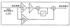
由数字混频器、数字相关器等组成;数字混频器的作用是将GPS射频前端输出的数字中频信号变换成I、Q两路数字零中频信号,便于后面进行基带信号解扩。It is composed of a digital mixer, a digital correlator, etc.; the function of the digital mixer is to convert the digital intermediate frequency signal output by the GPS RF front end into I and Q digital zero intermediate frequency signals, which is convenient for despreading the baseband signal later.
其中,数字混频器用乘法器实现。载波NCO的I、Q输出与输入信号在乘法器中进行数字下变频,于是去除输入信号载频而保留了用于基带相关的码。Among them, the digital mixer is realized with a multiplier. The I, Q output of the carrier NCO and the input signal are digitally down-converted in the multiplier, so the carrier frequency of the input signal is removed and the code used for baseband correlation is reserved.
其中,数字相关器由数字乘法器和积分-清除器构成;积分-清除器用一个双向(加法和减法)累加器实现,利用它对数字混频后输入信号与本地码相乘的每一个结果进行累加,经过0.2ms的积分累加后,输出一次相关累加值。积分-清除器的输入信号是数字下变频后的数据。再生伪码来自再生伪码发生器,当再生伪码为高电平时,则做加法运算;当再生伪码为低电平时,则做减法运算。在62MHz的上升沿进行累加运算,并在再生5K为高电平时,利用62MHz下降沿锁存输出一次0.2ms的累加结果,同时利用62MHz的上升沿进行同步置数。Among them, the digital correlator is composed of a digital multiplier and an integral-clearer; the integral-clearer is implemented with a two-way (addition and subtraction) accumulator, which is used to perform each result of multiplying the input signal and the local code after digital mixing. Accumulation, after 0.2ms integral accumulation, output a related accumulation value. The input signal to the integrator-scavenger is the digitally down-converted data. The regeneration pseudo-code comes from the regeneration pseudo-code generator. When the regeneration pseudo-code is high level, the addition operation is performed; when the regeneration pseudo-code is low level, the subtraction operation is performed. The accumulation operation is carried out on the rising edge of 62MHz, and when the regeneration 5K is high level, the 0.2ms accumulation result is latched and output once by the falling edge of 62MHz, and the number is set synchronously by using the rising edge of 62MHz.
下面对数字相关器的功能叙述如下:The function of the digital correlator is described as follows:
1)将锁频环载波NCO查找表输出的本地复制I,Q两路载波信号与数字中频信号幅度转换后的结果相乘,实现中频数字信号的下变频。1) Multiply the local copy I of the frequency-locked loop carrier NCO lookup table output, the Q two-way carrier signal and the result after the digital intermediate frequency signal amplitude conversion, and realize the down-conversion of the intermediate frequency digital signal.
2)下变频的结果利用码环的再生伪码发生器产生的各路再生伪码进行解扩,每0.2ms得到的积分清除结果输出(注意即时再生码积分清除20K结果的输出时间为每0.05ms输出一次),作为之后的锁频环鉴别器以及相位旋转模块的输入。2) The result of down-conversion is despread by using the regenerative pseudo-codes generated by the regenerative pseudo-code generator of the code ring, and the integral clearing result is output every 0.2ms (note that the output time of the instant regenerative code integral clearing 20K result is every 0.05 output once in ms), as the input of the subsequent frequency-locked loop discriminator and phase rotation module.
数字相关器的算法描述如下:The algorithm of the digital correlator is described as follows:
1)将锁频环载波NCO的输出Nco和幅度转换后的结果Adc下变频,就是将二者进行乘法运算,得到二进制表示的补码结果。硬件实现中调用了FPGA芯片中集成的硬件乘法器。1) Down-converting the output Nco of the frequency-locked loop carrier NCO and the result Adc after amplitude conversion is to perform multiplication of the two to obtain the complement result of binary representation. The hardware multiplier integrated in the FPGA chip is called in the hardware implementation.
2)积分清除的原理就是用一个累加器对数字下变频后输入信号与再生伪码相乘的每一位结果在系统时钟Clk62的上升沿进行累加,(伪码为‘1’乘以1,伪码为‘0’乘以-1,)经过0.2ms的积分累积后,在再生5KHz为高电平时,利用Clk62时钟的下降沿锁存积分清除结果并输出,同时利用62MHz的上升沿进行同步置数。2) The principle of integral clearing is to use an accumulator to accumulate each bit of the multiplication result of the input signal after digital down-conversion and the reproduced pseudo code on the rising edge of the system clock Clk62, (the pseudo code is '1' multiplied by 1, Pseudo-code is '0' multiplied by -1,) after 0.2ms of integral accumulation, when the regenerated 5KHz is high level, use the falling edge of the Clk62 clock to latch and clear the integration result and output it, and at the same time use the rising edge of 62MHz to synchronize set number.
数字相关器的接口描述如下:The interface description of the digital correlator is as follows:
模块内部接口:Module internal interface:
以下是积分清除模块的内部接口信号,包括复位信号,62MHz系统时钟以及数字中频幅度信号,另外还有锁频环NCO产生的载波正余弦幅度信号和再生伪码发生器产生的各路伪码。The following are the internal interface signals of the integration and clearing module, including reset signal, 62MHz system clock and digital intermediate frequency amplitude signal, as well as carrier sine and cosine amplitude signals generated by the frequency-locked loop NCO and various pseudocodes generated by the regenerative pseudocode generator.


模块外部接口:Module external interface:
以下是积分清除模块的外部接口信号,包括再生伪码发生器产生的再生5KHz时钟以及各路积分清除的结果。The following are the external interface signals of the integral clearing module, including the regenerated 5KHz clock generated by the regenerative pseudo code generator and the results of the integral clearing of each channel.

【2】载波锁频环处理单元【2】Carrier frequency locked loop processing unit
该单元包括载波相位累积器(carrier_phase_acc)和载波锁频环NCO查找表(fll_looker_nco)子单元。This unit includes a carrier phase accumulator (carrier_phase_acc) and a carrier frequency locked loop NCO lookup table (fll_looker_nco) subunit.
A.载波相位累积器(fll_phase_accum)模块设计A. Carrier phase accumulator (fll_phase_accum) module design
载波相位累积器硬件包括:预置寄存器、更新寄存器、累加器、累加结果寄存器、整周计数器组成。The hardware of the carrier phase accumulator includes: a preset register, an update register, an accumulator, an accumulative result register, and an entire cycle counter.
载波相位累积器功能描述:Carrier phase accumulator function description:
1)累加锁频环环路频率字与中频频率字,累加的结果作为锁频环载波NCO正余弦查找表的输入。1) The loop frequency word and the intermediate frequency frequency word of the frequency-locked loop are accumulated, and the accumulated result is used as the input of the frequency-locked loop carrier NCO sine-cosine lookup table.
2)累加锁频环环路频率字,输出锁频环多普勒载波累加器计数值。2) Accumulate the loop frequency word of the frequency-locked loop, and output the count value of the frequency-locked loop Doppler carrier accumulator.
载波相位累积器功能描述算法描述:Carrier Phase Accumulator Functional Description Algorithm Description:
1)在伪码再生5KHz同步时钟超前四个时钟周期的ReClk5K_E_4prd的高电平更新频率字。1) The frequency word is updated at the high level of ReClk5K_E_4prd which is four clock cycles ahead of the 5KHz synchronous clock reproduced in the pseudo code.
2)用系统时钟Clk62的上升沿对新的频率字和中频频率字进行累加,并取NCO累加结果的高12位作为查找表的输入;2) accumulate the new frequency word and the intermediate frequency frequency word with the rising edge of the system clock Clk62, and get the high 12 bits of the NCO accumulation result as the input of the look-up table;
3)用系统时钟Clk62的上升沿对新的频率字进行单独累加,取49位累加结果作为锁频环多普勒载波累加器计数值。3) Accumulate the new frequency word separately with the rising edge of the system clock Clk62, and take the 49-bit accumulation result as the frequency-locked loop Doppler carrier accumulator count value.
载波相位累积器接口描述Carrier Phase Accumulator Interface Description


B.载波锁频环NCO查找表(FLL_look_nco)模块设计B. Carrier frequency locked loop NCO lookup table (FLL_look_nco) module design
载波锁频环NCO查找表设置有频率控制字输入接口,载波环路通过不断调整载波锁频环NCO查找表的频率字来保持对接收信号载波频率和相位的跟踪。The NCO look-up table of the carrier frequency-locked loop is provided with a frequency control word input interface, and the carrier loop keeps track of the carrier frequency and phase of the received signal by continuously adjusting the frequency word of the NCO look-up table of the carrier frequency-locked loop.
载波锁频环NCO查找表要有足够的频率分辨率,保证能够高精度测量载波多普勒频率,这就要求载波锁频环NCO查找表要有足够的相位累加器字长,来满足频率分辨率的要求。载波锁频环NCO查找表的基准频率fs=62MHz。当载波锁频环NCO查找表的相位累加器字长为32位时,频率分辨率为δf=fclk/232=0.014Hz,可满足上面载波频率调整的需要。设频率控制字为W,则输出频率为The carrier frequency-locked loop NCO lookup table must have sufficient frequency resolution to ensure high-precision measurement of the carrier Doppler frequency, which requires the carrier frequency-locked loop NCO lookup table to have sufficient phase accumulator word length to meet the frequency resolution rate requirements. The reference frequency fs of the carrier frequency locked loop NCO look-up table is 62MHz. When the word length of the phase accumulator of the NCO lookup table of the carrier frequency locked loop is 32 bits, the frequency resolution is δf=fclk /232 =0.014Hz, which can meet the above carrier frequency adjustment needs. If the frequency control word is W, then the output frequency is
由于前面的相位累加的功能已经在载波相位累积器模块里面实现了,因此本部分只实现查找表的功能。Since the previous phase accumulation function has been implemented in the carrier phase accumulator module, this part only implements the look-up table function.
载波锁频环NCO查找表功能描述:Carrier frequency locked loop NCO lookup table function description:
根据载波相位累积器的输出,产生本地复制载波信号。Based on the output of the carrier phase accumulator, a local replica carrier signal is generated.
载波锁频环NCO查找表算法描述:Carrier frequency locked loop NCO lookup table algorithm description:
将载波相位累积器累加结果的高12位送入正余弦查找表(由ISE7.1生成的IP核)当中,输出的8位查表值在62MHz系统时钟的上升沿进行锁存。Send the upper 12 bits of the accumulated result of the carrier phase accumulator into the sine-cosine lookup table (IP core generated by ISE7.1), and the output 8-bit lookup table value is latched on the rising edge of the 62MHz system clock.
载波锁频环NCO查找表的接口描述:Interface description of carrier frequency locked loop NCO lookup table:


接口名称 方向 功能Interface Name Direction Function
Fll_Nco_Cos OUT 锁频环路NCO余弦输出Fll_Nco_Cos OUT frequency locked loop NCO cosine output
Fll_Nco_Sin OUT 锁频环路NCO正弦输出Fll_Nco_Sin OUT Frequency-locked loop NCO sine output
【3】载波锁相环(pll_loop_unit)处理单元[3] Carrier phase-locked loop (pll_loop_unit) processing unit
载波锁相环处理单元主要完成以下功能:The carrier phase-locked loop processing unit mainly completes the following functions:
1)接收外部复位控制信号(Reset),对自身进行复位,即返回至起始状态;1) Receive an external reset control signal (Reset), reset itself, that is, return to the initial state;
2)对输入的数字中频信号进行下变频、解扩以及积分清除,并提取0.2ms时刻的即时通道,超前滞后1/2、1/4通道的积分清除器结果给主信号处理器;2) Perform down-conversion, despreading and integral clearing on the input digital intermediate frequency signal, and extract the real-time channel at 0.2ms, and send the integral clearer results of the 1/2 and 1/4 channels leading and lagging to the main signal processor;
3)提取0.2ms时刻的载波整数、小数周相位,NCO累加结果寄存器的值给主信号处理器。3) Extract the integer and fractional cycle phase of the carrier at the time of 0.2ms, and send the value of the NCO accumulation result register to the main signal processor.
4)进行接收数据的解调,输出串行解调数据和帧同步信号。4) Demodulate the received data, and output serial demodulated data and frame synchronization signals.
该单元包括载波相位累积器(pll_phase_accum)与载波NCO查找表(pll_looker_nco)单元。This unit includes a carrier phase accumulator (pll_phase_accum) and a carrier NCO lookup table (pll_looker_nco) unit.
A载波相位累积器A carrier phase accumulator
载波相位累积器的功能描述Functional description of the carrier phase accumulator
累加锁相环环路频率字,输出锁相环多普勒载波累加器计数值,累加的结果的(31 downto20)共12位作为锁相环载波NCO正余弦查找表的输入。Accumulate the phase-locked loop loop frequency word, output the count value of the phase-locked loop Doppler carrier accumulator, and the total 12 bits of the accumulated result (31 downto20) are used as the input of the phase-locked loop carrier NCO sine-cosine lookup table.
载波相位累积器的算法描述Algorithm Description of Carrier Phase Accumulator
1)在伪码再生5KHz同步时钟超前四个时钟周期的ReClk5K_E_4prd的高电平更新频率字。1) The frequency word is updated at the high level of ReClk5K_E_4prd which is four clock cycles ahead of the 5KHz synchronous clock reproduced in the pseudo code.
2)用系统时钟Clk62的上升沿对新的频率字进行累加,取49位累加结果作为锁相环多普勒载波累加器计数值,并取NCO累加结果的(31 downto 20)共12位作为查找表的输入。2) Accumulate the new frequency word with the rising edge of the system clock Clk62, take the 49-bit accumulation result as the count value of the phase-locked loop Doppler carrier accumulator, and take the total 12 bits of the NCO accumulation result (31 downto 20) as Input to the lookup table.
载波相位累积器的接口描述Interface Description of Carrier Phase Accumulator


接口名称 方向 功能Interface Name Direction Function
ReClk5K_E_4prd IN 再生5K同步时钟超前4个时钟的置数时钟ReClk5K_E_4prd IN regenerates the 5K synchronous clock ahead of the set clock by 4 clocks
Pll_Pha_Int_dec OUT 锁相环整周、小数周计数值Pll_Pha_Int_dec OUT PLL full cycle, fractional cycle count value
B.载波锁相环NCO查找表(PLL_look_nco)模块设计B. Carrier phase-locked loop NCO lookup table (PLL_look_nco) module design
由于前面的相位累加的功能已经在载波相位累积器模块里面实现了,因此本部分只实现查找表的功能。Since the previous phase accumulation function has been implemented in the carrier phase accumulator module, this part only implements the look-up table function.
载波锁相环NCO查找表功能描述:Carrier phase locked loop NCO lookup table function description:
根据载波PLL相位累积器的输出,产生本地复制载波信号。Based on the output of the carrier PLL phase accumulator, a local replica carrier signal is generated.
载波锁相环NCO查找表:算法描述Carrier Phase Locked Loop NCO Lookup Table: Algorithm Description
将载波相位累积器累加结果的(31 downto 20)共12位送入正余弦查找表(生成的IP核)当中,输出的8位查表值在62MHz系统时钟的上升沿进行锁存。A total of 12 bits (31 down to 20) of the cumulative result of the carrier phase accumulator are sent to the sine-cosine lookup table (generated IP core), and the output 8-bit lookup table value is latched on the rising edge of the 62MHz system clock.
载波锁相环NCO查找表接口描述:Carrier phase-locked loop NCO lookup table interface description:


【4】再生伪码发生器单元模块设计【4】Regenerated Pseudocode Generator Unit Module Design
(1)功能(1) Function
再生伪码发生器单元是为伪码跟踪环路提供多路伪码的单元,它接收捕获电路部分给出的FFT快捕码片数,在时钟的推动下产生即时及超前、滞后分别为

再生伪码发生器的功能是:The functions of the regenerative pseudocode generator are:
1)接收外部复位控制信号(Reset),对自身进行复位,即返回至起始状态;1) Receive an external reset control signal (Reset), reset itself, that is, return to the initial state;
2)接收由码速率频率字、码环滤波器输出的频率字及载波辅助量频率字三部分组成的码频率控制字,用累加器计数,推动再生伪码的产生,通过查表得到伪码序列。2) Receive the code frequency control word composed of the code rate frequency word, the frequency word output by the code loop filter and the auxiliary frequency word of the carrier, count with the accumulator, promote the generation of the regenerated pseudo code, and obtain the pseudo code by looking up the table sequence.
3)用移位寄存器对再生伪码进行移位,得到所需的即时、超前、滞后伪码。3) Use the shift register to shift the reproduced pseudocode to obtain the required immediate, advanced and lagged pseudocodes.
4)输出即时码片计数及即时码相位。4) Output real-time chip count and real-time code phase.
(2)算法描述(2) Algorithm description
伪码的选择输出通过一个42位累加器模1023×1023来实现,高10位顺序对应1023个伪码码片,事先按相应顺序存储伪码组成码表,用高十位作为地址去查找码表,输出相应的伪码。The selection and output of the pseudo code is realized through a 42-bit accumulator modulo 1023×1023 , and the order of the upper 10 bits corresponds to 1023 pseudo code chips. Code table, output the corresponding pseudo-code.
(3)接口关系(3) Interface relationship


【5】位同步处理单元(Bit_sync_unit)【5】Bit synchronization processing unit (Bit_sync_unit)
(1)功能描述(1) Function description
测距信号的信息位和伪码周期是同步的。信息位速率是1kbps,每一位数据中包含1个伪码周期。数据位时钟对应伪码周期的起始位置。The information bits and pseudocode periods of the ranging signal are synchronized. The information bit rate is 1kbps, and each bit of data contains 1 pseudo-code period. The data bit clock corresponds to the start position of the pseudo code cycle.
(2)算法描述(2) Algorithm description
测距通道在跟踪环路锁定时,用作环路积分清除的再生5kHz时钟的上升沿对应伪码周期的起始位置。When the ranging channel is locked in the tracking loop, the rising edge of the regenerated 5kHz clock used for loop integral clearing corresponds to the initial position of the pseudo code period.
位同步模块由数字锁相环组成。数字锁相环根据本地估算的位同步时钟的相位误差,对本地估算出的位同步时钟相位进行连续不断的反馈调节,从而达到使本地估算的位同步时钟相位跟踪测距信号位同步时钟相位的目的。The bit synchronization module consists of a digital phase-locked loop. According to the phase error of the locally estimated bit synchronous clock, the digital phase-locked loop continuously feedbacks and adjusts the locally estimated bit synchronous clock phase, so as to make the locally estimated bit synchronous clock phase track the bit synchronous clock phase of the ranging signal Purpose.
I_Circum_sign为输入的数据流,对其进行符号判决,得到+1或者-1作为位同步数字锁相环的输入信号。I_Circum_sign is the input data stream, and its symbol is judged, and +1 or -1 is obtained as the input signal of the bit synchronous digital phase-locked loop.
(3)接口描述(3) Interface description

【6】帧同步处理单元(Frame_sync_unit)[6] Frame synchronization processing unit (Frame_sync_unit)
(1)功能描述(1) Function description
位同步结束后,需要进行数据解调。对位时钟内的10点数据累加,判断累加结果的符号,大于0此位判定为‘1’,小于0此位判定为‘0’。After the bit synchronization is completed, data demodulation is required. Accumulate the 10-point data in the bit clock, and judge the sign of the accumulation result. If it is greater than 0, it will be judged as '1', and if it is less than 0, it will be judged as '0'.
数据解调之后,同步数据帧的传输还需要实现帧同步,即要确定一帧数据传输开始的时刻。通过连续不断的检测帧同步字“EDE20”来确定数据帧的开始时刻。After data demodulation, the transmission of the synchronous data frame also needs to achieve frame synchronization, that is, to determine the moment when a frame of data transmission starts. The start moment of the data frame is determined by continuously detecting the frame synchronization word "EDE20".
(2)算法描述(2) Algorithm description
串行数据在位同步逻辑恢复出的位时钟的作用下,依次移入移位寄存器。将移位寄存器的内容与预知的固定帧同步字进行比较,如果两者相同,则输出高电平,否则保持低电平,这样,比较逻辑输出的高电平脉冲即为检测出来的帧同步脉冲。但是这样的结果不能直接输出,因为在数据帧的数据段中有可能出现伪帧同步字,从而导致输出虚假的帧同步脉冲,影响数据的正确接收。比较逻辑输出的高电平脉冲需要输入帧保护模块,消除虚假脉冲。The serial data is sequentially shifted into the shift register under the action of the bit clock recovered by the bit synchronization logic. Compare the content of the shift register with the predicted fixed frame synchronization word, if the two are the same, output a high level, otherwise keep a low level, so that the high level pulse output by the comparison logic is the detected frame synchronization pulse. But such a result cannot be output directly, because there may be a false frame synchronization word in the data segment of the data frame, which will lead to the output of a false frame synchronization pulse and affect the correct reception of data. The high-level pulse output by the comparison logic needs to be input to the frame protection module to eliminate false pulses.
帧保护模块在内部设立有一个帧同步状态标志,在初始时刻,该标志指示尚未得到真正的帧同步脉冲,即尚未实现帧同步。在接收到来自比较逻辑的第一个高脉冲(可能为帧同步脉冲)后,由于没有先验知识判定该脉冲是否为真正的帧同步脉冲,为了防止该帧数据丢失,假定它为真正的帧同步脉冲,将它输出。根据数据帧出现的规律,经过一段确知的时间后(1000个数据位),应该在确定的时刻能够检测到帧同步脉冲的出现。如果没能检测到高脉冲,则说明比较逻辑前次输出的高脉冲不是真正的帧同步脉冲,上述过程继续。如果连续3次都能在指定位置检测到帧同步脉冲,则认为已经完成帧同步任务,使帧同步状态标志指示已经实现帧同步。以后就只在预测的位置让比较逻辑产生的帧同步脉冲通过。The frame protection module has a frame synchronization status flag inside. At the initial moment, the flag indicates that the real frame synchronization pulse has not been obtained, that is, the frame synchronization has not been realized yet. After receiving the first high pulse (possibly a frame sync pulse) from the comparison logic, since there is no prior knowledge to determine whether the pulse is a true frame sync pulse, in order to prevent data loss for this frame, it is assumed to be a true frame Synchronization pulse, it is output. According to the law of data frame appearance, after a certain period of time (1000 data bits), the appearance of the frame synchronization pulse should be detected at a certain moment. If no high pulse is detected, it means that the high pulse output by the comparison logic last time is not a real frame synchronization pulse, and the above process continues. If the frame synchronization pulse can be detected at the specified position for 3 consecutive times, it is considered that the frame synchronization task has been completed, and the frame synchronization status flag indicates that the frame synchronization has been realized. The frame sync pulse generated by the comparison logic is then passed only at the predicted position.
在实现帧同步以后,仍旧在预测的时刻检测比较逻辑输出的高脉冲,如果连续3没能检测到预期的帧同步高脉冲,则认为失去帧同步,需要重启帧同步过程。After the frame synchronization is realized, the high pulse of the comparison logic output is still detected at the predicted time. If the expected frame synchronization high pulse cannot be detected for 3 consecutive times, the frame synchronization is considered to be lost, and the frame synchronization process needs to be restarted.
(3)接口描述(3) Interface description

3.DSP模块详细设计3. Detailed design of DSP module
其中,DSP模块的功能描述:Among them, the functional description of the DSP module:
(1)DSP程序加载完成后控制FPGA复位;(1) After the DSP program is loaded, the FPGA is reset;
(2)完成一路下行遥测和一路测距信号的环路处理:(2) Complete the loop processing of one downlink telemetry and one ranging signal:

从通道FPGA读取积分-清除器的0.2ms积分累加结果、相位旋转结果;Read the 0.2ms integral accumulation result and phase rotation result of the integral-clearer from the channel FPGA;

实现通道的载波锁频环、载波锁相环和码跟踪算法,控制载波锁频环、载波锁相环和码环跟踪锁定;Realize the carrier frequency locked loop, carrier phase locked loop and code tracking algorithm of the channel, and control the carrier frequency locked loop, carrier phase locked loop and code loop tracking and locking;
输出通道的锁频环NCO频率字、锁相环NCO频率字和码NCO频率字至前端通道FPGA;Output the frequency lock loop NCO frequency word, phase lock loop NCO frequency word and code NCO frequency word of the channel to the front-end channel FPGA;
(3)读取FFT快捕及测距通道前向处理FPGA内部存储器中的遥测数据、下获取下行测量信号的载波多普勒频率、数据位计数、伪码周期数、伪码相位、伪码CHIP相位、载波的整数周、载波相位、下行测量信号的信噪比以及下行测量帧数据;(3) Read the telemetry data in the FFT fast capture and ranging channel forward processing FPGA internal memory, obtain the carrier Doppler frequency of the downlink measurement signal, data bit count, pseudo code cycle number, pseudo code phase, pseudo code CHIP phase, integer cycle of carrier, carrier phase, signal-to-noise ratio of downlink measurement signal and downlink measurement frame data;
(4)处理控制命令:(4) Processing control commands:


其中,DSP信号处理器接口定义,如下表3所示:Among them, the DSP signal processor interface definition is shown in Table 3 below:

表3table 3
DSP信号处理器程序流程包括主程序、中断服务程序和环路处理程序三个组成部分,其中主程序包括初始化,中断控制,仲裁等。将载波和伪码的跟踪锁定过程放在10kHz中断程序内,只要有新数据来就立即进行环路跟踪。The program flow of DSP signal processor includes three components: main program, interrupt service program and loop processing program, among which the main program includes initialization, interrupt control, arbitration and so on. Put the tracking and locking process of the carrier and pseudo-code in the 10kHz interrupt program, and perform loop tracking immediately as long as new data comes.
下面对DSP模块的三部分组成详细说明如下:The following is a detailed description of the three parts of the DSP module:
DSP主程序流程说明(main)DSP main program flow description (main)
①程序描述①Program description
主程序是DSP后向通道处理软件程序中的主要部分,对DSP的外部存储器和中断的设置,完成对整个DSP软件程序的控制处理。The main program is the main part of the DSP back channel processing software program. It sets the external memory and interrupt of the DSP and completes the control and processing of the entire DSP software program.
②功能② function
主程序的主要功能是完成初始化工作和环路处理程序的循环控制,初始化工作包括CSL库的初始化,全局变量初始化。另外,主程序中还完成了中断的映射与设置。The main function of the main program is to complete the initialization work and the cycle control of the loop processing program. The initialization work includes the initialization of the CSL library and the initialization of global variables. In addition, the interrupt mapping and setting are also completed in the main program.
③输入项③Input items
FFT_Acqui_Flag:捕获状态标志FFT_Acqui_Flag: capture status flag
名称 类型 描述Name Type Description
FFT_Acqui_Flag int(整型) 0:未捕获FFT_Acqui_Flag int (integer) 0: not captured
1:捕获1: capture
INTR_0_2ms_Flag:软件中断标志INTR_0_2ms_Flag: Software interrupt flag
名称 类型 描述Name Type Description
INTR_0_2ms_Flag char(字符型) TRUE:中断发生INTR_0_2ms_Flag char (character type) TRUE: interrupt occurs
FALSE:中断清除FALSE: interrupt clear
④流程逻辑④ Process logic
首先进行开机初始化,包括CSL库函数的初始化,以及程序中所需要的全局变量的初始化;之后对环境变量进行设置,配置EMIF外部空间寄存器;再者,对外部中断进行设置,包括中断映射,复位,清除和使能。以上所有过程处理完之后,等待中断标志到来,然后判断中断所属的通道,再进行所属通道的环路处理,处理完后清除中断标志,再继续等待下一次中断的到来。First, start the boot initialization, including the initialization of the CSL library function, and the initialization of the global variables required in the program; then set the environment variables, configure the EMIF external space register; and then set the external interrupt, including interrupt mapping, reset , clear and enable. After all the above processes are processed, wait for the interrupt flag to arrive, then determine the channel to which the interrupt belongs, and then perform loop processing of the channel to which it belongs, clear the interrupt flag after processing, and continue to wait for the next interrupt to arrive.
DSP 0.2ms中断服务程序说明(FFT_0_2ms_Intr_ISR)DSP 0.2ms Interrupt Service Routine Description (FFT_0_2ms_Intr_ISR)
①程序描述①Program description
0.2ms中断服务程序是DSP对外部硬件中断的响应之后,读取所需外部接口数据而设计的。The 0.2ms interrupt service routine is designed after DSP responds to external hardware interrupts and reads the required external interface data.
②功能② function
中断服务程序的主要功能是通过开关中断的过程中完成外部数据的读入,另外,每开一次中断读取完数据后,将该通道软件中断标志置高,以备主程序进行环路处理的程序控制。The main function of the interrupt service program is to complete the reading of external data during the process of switching interrupts. In addition, after each interrupt is opened and the data is read, the software interrupt flag of the channel is set high to prepare for the loop processing of the main program. program control.
③性能③ performance
a)精度要求a) Accuracy requirements
积分清除结果寄存器取32位数据 Integral clear result register takes 32-bit data
相位旋转结果寄存器取32位数据 The phase rotation result register takes 32-bit data
其中,FPGA前向通道处理器输出的相位旋转结果位宽为36bit,DSP外部数据读取位宽只有32bit,一个数据要进行两次外部数据线读取再进行整合,在程序中相位旋转数据仍要保持36bit位宽。Among them, the bit width of the phase rotation result output by the FPGA to the channel processor is 36 bits, and the bit width of the DSP external data read is only 32 bits. One data needs to be read twice from the external data line and then integrated. In the program, the phase rotation data is still To keep 36bit bit width.
④输入项④Input items

前向通道处理FPGA 0.2ms积分清除结果寄存器Forward channel processing FPGA 0.2ms integral clear result register
I_PM_5K_ACCUM_ADDR(r)I_PM_5K_ACCUM_ADDR(r)
Q_PM_5K_ACCUM_ADDR(r)Q_PM_5K_ACCUM_ADDR(r)
格式:Format:
前向通道处理FPGA相位旋转结果寄存器Forward channel processing FPGA phase rotation result register
I_PM_5K_ROTATE_ADDR(r)I_PM_5K_ROTATE_ADDR(r)
Q_PM_5K_ROTATE_ADDR(r)Q_PM_5K_ROTATE_ADDR(r)
I_WE_5K_ROTATE_ADDR(r)I_WE_5K_ROTATE_ADDR(r)
Q_WE_5K_ROTATE_ADDR(r)Q_WE_5K_ROTATE_ADDR(r)
I_WL_5K_ROTATE_ADDR(r)I_WL_5K_ROTATE_ADDR(r)
Q_WL_5K_ROTATE_ADDR(r)Q_WL_5K_ROTATE_ADDR(r)
格式:Format:
前向通道处理FPGA FFT快捕结果寄存器Forward channel processing FPGA FFT quick capture result register
FFT_ACQUI_STATE_ADDR(r)FFT_ACQUI_STATE_ADDR(r)
格式:Format:
FFT_ACQUI_DOPP_ADDR(r)FFT_ACQUI_DOPP_ADDR(r)
格式:Format:
其中,r=1代表测距通道,r=0代表遥测通道Among them, r=1 represents the ranging channel, and r=0 represents the telemetry channel
⑤输出项⑤Output item

I_pm_5k_Accum_past[r]I_pm_5k_Accum_past[r]
Q_pm_5k_Accum_past[r]Q_pm_5k_Accum_past[r]
I_pm_5k_Accum_curr[r]I_pm_5k_Accum_curr[r]
Q_pm_5k_Accum_curr[r]Q_pm_5k_Accum_curr[r]
相位旋转结果 Phase rotation result
I_pm_5k_Rotate[r]I_pm_5k_Rotate[r]
Q_pm_5k_Rotate[r]Q_pm_5k_Rotate[r]
I_we_5k_Rotate[r]I_we_5k_Rotate[r]
Q_we_5k_Rotate[r]Q_we_5k_Rotate[r]
I_wl_5k_Rotate[r]I_wl_5k_Rotate[r]
Q_wl_5k_Rotate[r]Q_wl_5k_Rotate[r]

FFT_Acqui_State[r]FFT_Acqui_State[r]
FFT_Acqui_Dopp_Word[r]FFT_Acqui_Dopp_Word[r]
0.2ms中断发生标志 0.2ms interrupt occurrence flag
Irq_01ms_Flag[r]Irq_01ms_Flag[r]
其中,r=1代表测距通道,r=0代表遥测通道Among them, r=1 represents the ranging channel, and r=0 represents the telemetry channel
⑥流程逻辑⑥Process logic
进入中断服务程序后,首先将外部中断关闭后清除即保护现场,然后保存前一次通道积分清除结果,读取当前通道积分清除结果、相位旋转结果,并将中断标志变量置为有效,最后打开中断,恢复现场后退出中断。DSP后向通道处理的软件程序设计中,对于0.2ms的中断服务程序的设计分为测距通道0.2ms中断服务程序和遥测通道0.2ms中断服务程序。After entering the interrupt service routine, first close the external interrupt and clear it to protect the site, then save the previous channel integral clearing result, read the current channel integral clearing result and phase rotation result, and set the interrupt flag variable to be valid, and finally open the interrupt , to resume the scene after exiting the interrupt. In the software program design of DSP back channel processing, the design of 0.2ms interrupt service program is divided into ranging channel 0.2ms interrupt service program and telemetry channel 0.2ms interrupt service program.
⑦接口⑦Interface
中断服务程序与主程序之间的接口:软件中断标志、捕获状态标志;The interface between the interrupt service routine and the main program: software interrupt flag, capture status flag;
中断服务程序与环路处理程序的接口:积分清除数据、相位旋转数据、捕获多普勒频率字。Interfacing of Interrupt Service Routine to Loop Handler: Integrate Clear Data, Phase Rotate Data, Capture Doppler Frequency Word.
DSP通道环路处理流程说明(LOOP_TRACK_FUNC)DSP channel loop processing flow description (LOOP_TRACK_FUNC)
环路处理开始后,首先对环路状态进行确定,如果处于锁定或跟踪状态,则进行下一步的处理;After the loop processing starts, first determine the loop state, if it is in the locked or tracking state, proceed to the next step;
环路计数器控制整个环路的处理进程,为单向计数,每进入一次环路处理,也即每来一次中断读取新数据后对环路计数器加1。The loop counter controls the processing process of the entire loop, which is one-way counting, and adds 1 to the loop counter every time it enters the loop processing, that is, every time an interrupt comes to read new data.
FLL处理中,由FLL门限切换标志控制FLL鉴频器采用10K积分清除数据还是20K积分清除数据,接着对鉴频结果进行环路滤波,输出FLLNCO控制字;In FLL processing, the FLL discriminator is controlled by the FLL threshold switching flag to use 10K integrals to clear data or 20K integrals to clear data, and then perform loop filtering on the frequency discrimination results, and output the FLLNCO control word;
PLL处理中,鉴相器采用二象限鉴相,鉴相结果通过环路滤波器输出PLLNCO控制字;In PLL processing, the phase detector adopts two-quadrant phase detection, and the phase detection result outputs the PLLNCO control word through the loop filter;
DDLL处理中,对于码相位的鉴别中要有一步归整的处理,即鉴别结果超前2个码片则归为+2,滞后2个码片则归为-2;鉴别结果通过环路滤波再由载波辅助的处理后输出DDLLNCO控制字;In DDLL processing, there must be a one-step rounding process in the identification of the code phase, that is, the identification result is classified as +2 if it is ahead of 2 chips, and it is classified as -2 if it is 2 chips behind; Output DDLLNCO control word after carrier-assisted processing;
①程序描述①Program description
环路处理程序为DSP后向处理的核心部分,实现数据鉴别算法,环路滤波算法,处理完后得到的数据要向FPGA前向通道处理器输出,以完成整个跟踪过程。The loop processing program is the core part of the DSP backward processing, which realizes the data identification algorithm and the loop filtering algorithm. After processing, the data obtained will be output to the FPGA forward channel processor to complete the entire tracking process.
②功能② function
环路处理程序在捕获模块的伪码相位预测值和多普勒频率预测值的基础之上,进行伪码相位的跟踪和载波相位的锁定跟踪,主要完成FLL鉴别算法,FLL环路滤波算法,PLL鉴别算法,PLL环路滤波算法,DDLL鉴别算法,DDLL环路滤波算法,FLL锁定判决,PLL锁定判决,DDLL锁定判决。The loop processing program performs the tracking of the pseudo-code phase and the locking and tracking of the carrier phase on the basis of the predicted value of the pseudo-code phase and the predicted value of the Doppler frequency of the capture module. It mainly completes the FLL identification algorithm, the FLL loop filter algorithm, PLL discrimination algorithm, PLL loop filter algorithm, DDLL discrimination algorithm, DDLL loop filter algorithm, FLL lock judgment, PLL lock judgment, DDLL lock judgment.
③性能③ performance


其中,r=1代表测距通道,r=0代表遥测通道Among them, r=1 represents the ranging channel, and r=0 represents the telemetry channel
④输入项④Input item

I_pm_5k_Accum_past[r]I_pm_5k_Accum_past[r]
Q_pm_5k_Accum_past[r]Q_pm_5k_Accum_past[r]
I_pm_5k_Accum_curr[r]I_pm_5k_Accum_curr[r]
Q_pm_5k_Accum_curr[r]Q_pm_5k_Accum_curr[r]
格式:Format:

I_pm_5k_Rotate[r]I_pm_5k_Rotate[r]
Q_pm_5k_Rotate[r]Q_pm_5k_Rotate[r]
I_we_5k_Rotate[r]I_we_5k_Rotate[r]
Q_we_5k_Rotate[r]Q_we_5k_Rotate[r]
I_wl_5k_Rotate[r]I_wl_5k_Rotate[r]
Q_wl_5k_Rotate[r]Q_wl_5k_Rotate[r]
格式:Format:

FFT_Acqui_Dopp_Word[r]FFT_Acqui_Dopp_Word[r]
格式:Format:
其中,r=1代表测距通道,r=0代表遥测通道Among them, r=1 represents the ranging channel, and r=0 represents the telemetry channel
⑤输出项⑤Output item

FLL_NCO_WORD_ADDR(r)FLL_NCO_WORD_ADDR(r)
格式:Format:


PLL_NCO_WORD_ADDR(r)PLL_NCO_WORD_ADDR(r)
格式:Format:

DDLL_NCO_WORD_ADDR(r)DDLL_NCO_WORD_ADDR(r)
格式:Format:
状态寄存器 status register
STATE_REGISTER_ADDR(r)STATE_REGISTER_ADDR(r)
格式:Format:
其中,r=1代表测距通道,r=0代表遥测通道Among them, r=1 represents the ranging channel, and r=0 represents the telemetry channel
⑥锁频环跟踪模块(FLL_TRACK_FUNC)⑥ Frequency-locked loop tracking module (FLL_TRACK_FUNC)
该模块中实现的功能:FLL鉴别算法,FLL环路滤波算法。Functions implemented in this module: FLL identification algorithm, FLL loop filtering algorithm.
⑦输入项⑦Input items

I_pm_5k_Accum_past[r]I_pm_5k_Accum_past[r]
Q_pm_5k_Accum_past[r]Q_pm_5k_Accum_past[r]
I_pm_5k_Accum_curr[r]I_pm_5k_Accum_curr[r]
Q_pm_5k_Accum_curr[r]Q_pm_5k_Accum_curr[r]
格式:Format:

FFT_Acqui_Dopp_Word[r]FFT_Acqui_Dopp_Word[r]
格式:Format:
其中,r=1代表测距通道,r=0代表遥测通道Among them, r=1 represents the ranging channel, and r=0 represents the telemetry channel
⑧输出项⑧Output item

FLL_NCO_WORD(r)FLL_NCO_WORD(r)
格式:Format:
其中,r=1代表测距通道,r=0代表遥测通道Among them, r=1 represents the ranging channel, and r=0 represents the telemetry channel
另外,锁频环算法:锁频环鉴别器采用点交叉鉴频算法,公式如下:In addition, the frequency-locked loop algorithm: the frequency-locked loop discriminator adopts the point cross-discrimination algorithm, and the formula is as follows:
为了获得更大的鉴频范围,锁频环先采用20K鉴频,而后采用10K鉴频。对于20K鉴频,反正切采用四象限算法;对于10K鉴频,反正切采用二象限算法。根据式(24)(25),忽略噪声后,代入(2)式,得:In order to obtain a larger frequency discrimination range, the frequency locked loop adopts 20K frequency discrimination first, and then adopts 10K frequency discrimination. For 20K frequency discrimination, arctangent adopts four-quadrant algorithm; for 10K frequency discrimination, arctangent adopts two-quadrant algorithm. According to formulas (24) and (25), after ignoring the noise, substituting into formula (2), we get:
根据三角和差公式,得:According to the trigonometric sum and difference formula, we get:
再由θ(k)-θ(k-1)=2πTΔfd,T为积分清除时间,采用20K时,T=0.05ms;采用10K时,T=0.2ms。所以锁频环鉴别算法的结果为efk=Δfd,其中,即信号实际多普勒频率与本地估计多普勒频率的差值。Then θ(k)-θ(k-1)=2πTΔfd , T is the integral clearing time, when 20K is used, T=0.05ms; when 10K is used, T=0.2ms. Therefore, the result of the frequency-locked loop identification algorithm is efk =Δfd , where, That is, the difference between the actual Doppler frequency of the signal and the locally estimated Doppler frequency.
锁频环路滤波算法Frequency Locked Loop Filtering Algorithm
对于相同阶数的跟踪环路,相对锁相环和码环中采用的滤波器,锁频环的滤波器需要增加一个积分器。For tracking loops of the same order, compared to the filters used in phase-locked loops and code loops, the filter of the frequency-locked loop needs to add an integrator.
锁频环相对于锁相环,对动态的应力较好。为应对同样的动态,锁频环的阶数可以比锁相环的阶数低一阶。所以载波跟踪锁频环采用二阶环路,一阶滤波器实现。Frequency-locked loops are better for dynamic stress than phase-locked loops. To cope with the same dynamics, the frequency-locked loop can be one order lower than the phase-locked loop. Therefore, the carrier tracking frequency-locked loop adopts a second-order loop and a first-order filter.
一阶最优环路滤波器为:The first-order optimal loop filter is:
其中,Kd=1,为频率鉴别器的增益,
相应的载波环的滤波器为:The corresponding carrier loop filter is:
采用数字矩形积分映像方式,其映射关系为:
二阶载波环路滤波器的离散传递函数为:The discrete transfer function of the second-order carrier loop filter is:
其实域对应表达式为:In fact, the corresponding expression of the field is:
其中,T-为滤波器输入采样时间间隔,T=0.1ms;Among them, T- is the filter input sampling time interval, T=0.1ms;
ωn-为环路的自然频率,ωn=1.89BLF,BLF为环路的带宽。ωn - is the natural frequency of the loop, ωn =1.89BLF , and BLF is the bandwidth of the loop.
①输入项①Input items
相位旋转结果 Phase rotation result
I_pm_10k_Rotate[r]I_pm_10k_Rotate[r]
Q_pm_10k_Rotate[r]Q_pm_10k_Rotate[r]
格式:Format:
其中,r=1代表测距通道,r=0代表遥测通道Among them, r=1 represents the ranging channel, and r=0 represents the telemetry channel
②输出项② output items

PLL_NCO_WORD(r)PLL_NCO_WORD(r)
格式:Format:
其中,r=1代表测距通道,r=0代表遥测通道Among them, r=1 represents the ranging channel, and r=0 represents the telemetry channel
锁相环算法:PLL algorithm:
对经过解调、解扩后的信号进行积分清除,经过相位旋转,采用锁相环进一步消除频差和相位差,相位旋转如下实现:The signal after demodulation and despreading is integrated and cleared, and after phase rotation, the phase-locked loop is used to further eliminate the frequency difference and phase difference. The phase rotation is realized as follows:
选择
锁相环环路滤波算法采用二阶环路滤波器,即三阶跟踪环路,其最优环路滤波器为:The phase-locked loop loop filtering algorithm uses a second-order loop filter, that is, a third-order tracking loop, and its optimal loop filter is:
其中,ωnp为环路的自然频率;Kd为鉴相器增益(Kd=1);Kv为NCO增益其中
采用数字矩形积分映像方式,其映射关系为:
环路滤波器的离散传递函数为:The discrete transfer function of the loop filter is:
其时域对应表达式为:Its corresponding expression in the time domain is:
其中,ωnP=1.2BLF,BLF为跟踪环路带宽,T是环路滤波器采样时间间隔(等于环路更新时间)。Wherein, ωnP =1.2BLF , BLF is the bandwidth of the tracking loop, and T is the sampling time interval of the loop filter (equal to the update time of the loop).
码环跟踪模块(DDLL_TRACK_FUNC)Code ring tracking module (DDLL_TRACK_FUNC)
该模块完成的功能有:DDLL鉴别算法,DDLL环路滤波算法。The functions completed by this module are: DDLL identification algorithm, DDLL loop filtering algorithm.
①输入项①Input item

I_pm_5k_Rotate[r]I_pm_5k_Rotate[r]
Q_pm_5k_Rotate[r]Q_pm_5k_Rotate[r]
I_we_5k_Rotate[r]I_we_5k_Rotate[r]
Q_we 5k_Rotate[r]Q_we 5k_Rotate[r]
I_wl_5k_Rotate[r]I_wl_5k_Rotate[r]
Q_wl_5k_Rotate[r]Q_wl_5k_Rotate[r]
格式:Format:
锁频环NCO频率字 Frequency locked loop NCO frequency word
FLL_NCO_WORD(r)FLL_NCO_WORD(r)
格式:Format:
锁相环NCO频率字 PLL NCO frequency word
PLL_NCO_WORD(r)PLL_NCO_WORD(r)
格式:Format:
其中,r=1代表测距通道,r=0代表遥测通道Among them, r=1 represents the ranging channel, and r=0 represents the telemetry channel
②输出项② output items

DDLL_NCO_WORD(r)DDLL_NCO_WORD(r)
格式:Format:
其中,r=1代表测距通道,r=0代表遥测通道Among them, r=1 represents the ranging channel, and r=0 represents the telemetry channel
伪码跟踪环算法:Pseudo-code tracking loop algorithm:
该码跟踪环鉴别算法采用点积鉴别算法,采用“归一化”操作,这样做的好处是能有效减少幅度敏感性,同时在适当信噪比条件下提供不变的鉴别器增益,有助于确定跟踪环路的增益。The code tracking loop identification algorithm adopts the dot product identification algorithm and adopts the "normalization" operation. The advantage of this is that it can effectively reduce the amplitude sensitivity, and at the same time provide a constant discriminator gain under the condition of an appropriate signal-to-noise ratio, which is helpful. to determine the gain of the tracking loop.
归一化的点积鉴别器算法如下:The normalized dot product discriminator algorithm is as follows:
式中,Ies(k)、Ips(k)、Ils(k)分别为输入同相数字信号与超前码、实时码及滞后码在数字相关积累后的输出,Qes(k)、Qps(k)、Qls(k)分别为输入正交数字信号与超前码、实时码、滞后码在数字相关积累后的输出。In the formula, Ies (k), Ips (k), Ils (k) are the outputs of the input in-phase digital signal and the lead code, real-time code and lag code after digital correlation accumulation, Qes (k), Qps (k), Qls (k) are the outputs of the input quadrature digital signal and the lead code, real-time code, and lag code after digital correlation accumulation respectively.
码环路滤波器code loop filter
伪码跟踪环路采用二阶环路,参考GPS系统的设计,其最优环路传递函数为:The pseudo-code tracking loop adopts a second-order loop. Referring to the design of the GPS system, the optimal loop transfer function is:
二阶环路对应的一阶滤波器为:The first-order filter corresponding to the second-order loop is:
采用数字矩形积分映像方式,其映射关系为:
二阶DDLL环路的一阶数字滤波器的离散传递函数为:The discrete transfer function of the first-order digital filter for the second-order DDLL loop is:
时域对应表达式为:The corresponding expression in the time domain is:
其中,ωn-为环路滤波器的自然角频率,ωn=1.89BLF,BLF=2为环路带宽;T-为环路滤波器输入采样时间间隔(等于环路更新时间);Wherein, ωn -is the natural angular frequency of the loop filter, ωn =1.89BLF , BLF =2 is the loop bandwidth; T-is the loop filter input sampling time interval (equal to the loop update time);
K=KdKv为环路滤波器增益。Kd=2为鉴相器增益,

本发明一种高动态扩频精密测距接收机,其优点及功效在于:本发明测距精度高,误差小,通信中抗干扰能力高,测控精确。The invention provides a highly dynamic spread spectrum precision ranging receiver, and its advantages and effects are: the invention has high ranging precision, small error, high anti-interference ability in communication, and accurate measurement and control.
(四)附图说明:(4) Description of drawings:
图1所示为送出IFFT结果的时序Figure 1 shows the timing of sending IFFT results
图2所示为频率细搜的流程Figure 2 shows the process of frequency fine search
图3所示为伪码快捕单元的划分及其接口信号Figure 3 shows the division of the pseudo-code quick capture unit and its interface signals
图4所示为载波相位累积器的硬件实现Figure 4 shows the hardware implementation of the carrier phase accumulator
图5所示为再生伪码发生器硬件实现Figure 5 shows the hardware implementation of the regenerative pseudocode generator
图6所示为帧同步实现结构Figure 6 shows the frame synchronization implementation structure
图7所示为DSP信号处理器主程序流程Figure 7 shows the main program flow of the DSP signal processor
图8所示为0.2ms中断服务程序Figure 8 shows the 0.2ms interrupt service routine
图9所示为中断服务程序接口示意图Figure 9 shows a schematic diagram of the interrupt service program interface
图10所示为通道跟踪处理流程Figure 10 shows the channel tracking process flow
图11所示为二阶载波环路的滤波器模拟实现Figure 11 shows a simulated implementation of a filter for a second-order carrier loop
图12所示为二阶FLL的环路滤波器数字实现Figure 12 shows a digital implementation of a loop filter for a second-order FLL
图13所示为三阶PLL跟踪环路中的滤波器模拟实现Figure 13 shows the simulated implementation of the filter in the third-order PLL tracking loop
图14所示为一阶滤波器模拟实现Figure 14 shows the analog implementation of a first-order filter
图15所示为一阶滤波器数字实现Figure 15 shows a digital implementation of a first-order filter
图16所示为环路处理流程图Figure 16 shows the loop processing flow chart
图17所示为环路处理程序接口示意图Figure 17 shows a schematic diagram of the loop handler interface
(五)具体实施方式:(5) Specific implementation methods:
本发明一种高动态扩频精密测距接收机,采用灵活的现场可编程门阵列+数字信号处理(即FPGA+DSP)的结构,实现全数字化操作。其主要包括FPGA及DSP两大模块。The present invention is a highly dynamic spread spectrum precision ranging receiver, which adopts the structure of flexible field programmable gate array + digital signal processing (namely FPGA + DSP) to realize full digital operation. It mainly includes two modules of FPGA and DSP.
1.FPGA硬件模块设计1. FPGA hardware module design
FPGA模块采用自顶向下的设计方法,按照外部接口——内部功能模块的信息流设计,主要由FPGA外部接口、FPGA接收模块构成。The FPGA module adopts a top-down design method, and is designed according to the information flow of the external interface-internal functional module, and is mainly composed of the FPGA external interface and the FPGA receiving module.
(1)FPGA外部接口模块设计,包括:(1) FPGA external interface module design, including:
FPGA与DSP接口:完成与DSP-EMIF之间数据总线、地址总线、控制总线连接,其中控制总线中含有片选、读写控制、输出使能、系统复位等信号线;DSP可以通过数据总线对FPGA内部寄存器、存储空间进行读写操作;DSP通过地址总线进行地址译码对FPGA内部进行寻址操作。FPGA and DSP interface: complete the data bus, address bus, and control bus connection with DSP-EMIF, in which the control bus contains signal lines such as chip selection, read and write control, output enable, and system reset; DSP can communicate with the DSP through the data bus. The FPGA internal registers and storage space perform read and write operations; the DSP performs address decoding through the address bus to perform addressing operations within the FPGA.
FPGA与射频前端接口:射频前端信号通过ADC采样后,得到数字信号,在FPGA内部进行数字信号锁存后,进行数字信号处理。FPGA and RF front-end interface: After the RF front-end signal is sampled by the ADC, a digital signal is obtained, and after the digital signal is latched inside the FPGA, the digital signal is processed.
FPGA载波、伪码模拟信号接口:输出含有载波多谱勒的数字信号,通过DAC与带通滤波器BPF后,进行电平调节,送给射频前端;FPGA carrier, pseudo-code analog signal interface: output digital signal containing carrier Doppler, after passing through DAC and band-pass filter BPF, adjust the level and send it to the RF front end;
系统工作时钟接口:接收射频前端输出的系统工作时钟;System working clock interface: receive the system working clock output by the RF front end;
1PPS时钟基准输出接口:输出本地1PPS秒脉冲时间基准;1PPS clock reference output interface: output local 1PPS second pulse time reference;
1PPS可调时间输出接口:输出本地调整1PPS秒脉冲时间;1PPS adjustable time output interface: output local adjustment of 1PPS second pulse time;
1PPM可调时间输出接口:输出本地调整1PPM分秒冲时间;1PPM adjustable time output interface: output local adjustment of 1PPM minute and second rush time;
(2)FPGA接收模块设计(2) FPGA receiving module design
①模块功能:该模块主要完成扩频信号的捕获、跟踪与解扩解调,进行伪距提取、通信数据再生恢复、与纠错重组。①Module function: This module mainly completes the acquisition, tracking, despreading and demodulation of spread spectrum signals, and performs pseudorange extraction, communication data regeneration and recovery, and error correction and reorganization.
②模块输入信号:数字中频信号、系统工作时钟、积分清零信号、系统复位信号等;② Module input signal: digital intermediate frequency signal, system working clock, integral reset signal, system reset signal, etc.;
③模块输出信号:系统载波与伪码捕获跟踪状态、再生通信数据、伪距测量结果与再生帧同步脉冲等。③ Module output signal: system carrier and pseudocode capture tracking status, regenerated communication data, pseudorange measurement results and regenerated frame synchronization pulse, etc.
④FPGA接收模块主要构成单元包括:④ The main components of the FPGA receiving module include:
伪码快捕单元 Pseudo code quick capture unit


其中,伪码快捕单元:接收AD转换电路输出的数字中频信号,产生再生载波对数字中频信号进行下变频,完成载波剥离;采用FFT方法实现相关运算;对相关结果进行检测判决,并计算信噪比;在捕获完成时获得扩频信号的伪码相位和载波多普勒频移的粗略估计,将其与捕获状态(是否检测到信号)一起输出给载波和码跟踪电路。由于采用基2-FFT运算要求数据点数为2的次幂,故在相关运算前需要对下变频结果进行内差和抽取操作。Among them, the pseudo-code quick capture unit: receives the digital intermediate frequency signal output by the AD conversion circuit, generates a regenerated carrier to down-convert the digital intermediate frequency signal, and completes the carrier stripping; uses the FFT method to achieve correlation operations; detects and judges the correlation results, and calculates the signal Noise ratio; obtain the pseudo-code phase of the spread spectrum signal and a rough estimate of the carrier Doppler frequency shift when the acquisition is completed, and output it to the carrier and code tracking circuit together with the acquisition status (whether the signal is detected or not). Since the radix-2-FFT operation requires the number of data points to be a power of 2, it is necessary to perform interpolation and extraction operations on the down-conversion results before the correlation operation.
伪码快捕单元的性能要求:The performance requirements of the pseudocode quick capture unit:
动态范围:载波频率变化范围≤±6kHz(C/N0≥48dB/Hz);频率变化速率≤±450Hz/s(C/N0≥48dB/Hz);码速率偏差≤±5HzDynamic range: carrier frequency range ≤±6kHz (C/N0 ≥48dB/Hz); frequency change rate ≤±450Hz/s (C/N0 ≥48dB/Hz); code rate deviation ≤±5Hz
捕获时间:≤±5s(C/N0≥48dB/Hz)Capture time: ≤±5s (C/N0 ≥48dB/Hz)
电平变化范围:30dBLevel change range: 30dB
抗干扰能力:单频干扰,干信比10dB,性能不恶化Anti-interference ability: single-frequency interference, interference-to-signal ratio 10dB, performance does not deteriorate
伪码快捕单元的接口要求:The interface requirements of the pseudo code quick capture unit:
接口信号列表如下面表1所示:The interface signal list is shown in Table 1 below:

表1Table 1
伪码快捕单元接口信号的统一约定:The unified agreement of the interface signal of the pseudo-code quick capture unit:
(a)伪码快捕单元与外部模块的接口信号,以及内部的FFT相关器和信号检测模块之间的接口信号,见下面的图“伪码快捕单元的划分及其接口信号”所示,图中同时标明了各信号的方向及位宽。(a) The interface signal between the pseudo-code fast capture unit and the external module, as well as the interface signal between the internal FFT correlator and the signal detection module, see the following figure "Division of the pseudo-code fast capture unit and its interface signals" , and the direction and bit width of each signal are marked in the figure.
(b)在上述信号中,复位信号为低有效,并采用同步复位。(b) Among the above signals, the reset signal is active low and adopts synchronous reset.
(c)下面的信号均为高有效,且仅持续一个62MHz时钟周期:(c) The following signals are all active high and only last for one 62MHz clock cycle:


(d)捕获状态(是否检测到信号)指示信号为高时,指示检测到信号,输出结果有效,并一直持续到下一次复位伪码快捕单元。(d) When the capture state (whether the signal is detected) indicates that the signal is high, it indicates that the signal is detected, and the output result is valid, and continues until the next reset of the pseudo-code quick capture unit.
(e)预置伪码的写使能为高有效。(e) The write enable of the preset pseudocode is active high.
其中,整个伪码快捕单元的工作流程如下:Among them, the workflow of the entire pseudo-code fast-catching unit is as follows:
(a)复位整个FFT捕获模块,然后信号检测模块始终送出要搜索载频值上的本地载波给FFT相关器模块。(a) Reset the entire FFT acquisition module, and then the signal detection module always sends the local carrier on the carrier frequency value to be searched to the FFT correlator module.
(b)将预置伪码的写使能置高,并根据预置伪码的写地址将预置伪码逐一写入,然后给出伪码预置完毕信号;FFT相关器模块在码NCO的推动下,将伪码读出,并进行FFT运算,将FFT结果缓存。(b) Set the write enable of the preset pseudo-code high, and write the preset pseudo-code one by one according to the write address of the preset pseudo-code, and then give the pseudo-code preset completion signal; the FFT correlator module is in the code NCO Under the impetus of , the pseudo code is read out, and the FFT operation is performed, and the FFT result is cached.
(c)信号检测模块在收到启动捕获的命令后,每隔0.2ms产生一个时间基准信号给FFT相关器模块,并送出启动FFT相关器计算的信号。FFT相关器模块在收到启动信号后,等待下一个0.2ms基准信号到来时,开始对AD采样信号进行下变频、内插和缓存,然后计算其FFT,并将本地伪码FFT结果和接收信号FFT结果共轭相乘,再进行IFFT。IFFT计算完毕后,送出IFFT计算完成信号和IFFT结果的指数项,在接下来的时钟周期内逐一送出4096点IFFT结果的尾数项(包括实部和虚部)和对应的索引值(取值为0~4095)。送出IFFT结果的时序如图1所示。之后,FFT相关器模块就可以接收下一次启动FFT相关器计算的信号了。(c) After receiving the command to start capture, the signal detection module generates a time reference signal every 0.2ms to the FFT correlator module, and sends a signal to start the calculation of the FFT correlator. After the FFT correlator module receives the start signal and waits for the next 0.2ms reference signal to arrive, it starts to down-convert, interpolate and buffer the AD sampling signal, then calculates its FFT, and compares the local pseudocode FFT result with the received signal The FFT results are conjugate multiplied, and then IFFT is performed. After the IFFT calculation is completed, send the IFFT calculation completion signal and the exponent item of the IFFT result, and send the mantissa item (including the real part and the imaginary part) of the 4096-point IFFT result one by one in the next clock cycle and the corresponding index value (the value is 0~4095). The sequence of sending IFFT results is shown in Figure 1. After that, the FFT correlator module can receive the signal for starting the calculation of the FFT correlator next time.
(d)从上到下各波形依次为IFFT计算完成信号、IFFT结果的实部尾数项、IFFT结果的虚部尾数项、IFFT结果对应的索引值。信号检测模块在收到IFFT结果后,进行求模和积累。在进行最后一次积累时,还要进行峰值检测;在积累完毕后,再进行噪声功率估计,最后将峰值、峰值对应的位置和噪声功率估计值送给唐检测器。如果唐检测器在预定相位区间内未检测到信号,则改变载频值重复步骤③和④;如果当搜索完所有频点时,仍未检测到信号,则将0.2ms基准信号滞后0.02ms,再重复步骤③和④来搜索所有频点;如果在各个延迟值的0.2ms基准信号和所有载频值上都搜索完毕后,仍未捕获到信号,则宣告未捕获到信号,退出捕获过程,同时给出状态指示(捕获计算完毕但未检测到信号)。如果唐检测器检测到信号,则转入(e)进行频率细搜(d) The waveforms from top to bottom are the IFFT calculation completion signal, the real mantissa item of the IFFT result, the imaginary mantissa item of the IFFT result, and the corresponding index value of the IFFT result. After receiving the IFFT result, the signal detection module performs modulo calculation and accumulation. During the last accumulation, peak detection is also performed; after the accumulation is completed, noise power estimation is performed, and finally the peak value, the position corresponding to the peak value and the estimated value of noise power are sent to the Tang detector. If the Tang detector does not detect a signal within the predetermined phase interval, change the carrier frequency value and repeat steps ③ and ④; if no signal is detected when all frequency points are searched, then delay the 0.2ms reference signal by 0.02ms, Repeat steps ③ and ④ to search all frequency points; if the signal is still not captured after searching the 0.2ms reference signal of each delay value and all carrier frequency values, declare that no signal has been captured, and exit the capture process. At the same time, a status indication is given (acquisition calculation is completed but no signal is detected). If the Tang detector detects a signal, then go to (e) for frequency fine search
(e)频率细搜,流程如图2所示(e) Frequency fine search, the process is shown in Figure 2
整个伪码快捕单元可划分为FFT相关器模块和信号检测模块两个模块,如图3所示:The entire pseudocode quick capture unit can be divided into two modules, the FFT correlator module and the signal detection module, as shown in Figure 3:
其中,FFT相关器完成对接收信号的内插和缓存;对内插后的接收信号进行FFT计算;产生本地伪码并对C码进行FFT计算;将信号FFT的结果和伪码FFT的结果共轭相乘;对共轭相乘的结果做IFFT并输出。信号检测模块对接收到的IFFT结果进行求模、积累、选大,并估计噪声功率;进行唐检测判决;在检测到信号后完成频率细搜。Among them, the FFT correlator completes the interpolation and buffering of the received signal; performs FFT calculation on the received signal after interpolation; generates the local pseudo code and performs FFT calculation on the C code; Conjugate multiplication; perform IFFT on the result of conjugate multiplication and output. The signal detection module calculates, accumulates, and selects the received IFFT results, and estimates the noise power; performs Tang detection and judgment; completes the frequency search after the signal is detected.
其中,FFT相关器模块的设计如下:Among them, the design of the FFT correlator module is as follows:
FFT相关器模块包括下变频和抽取模块,以及FFT/IFFT计算模块两部分组成。The FFT correlator module consists of two parts: the down-conversion and extraction module, and the FFT/IFFT calculation module.
(a)下变频和抽取模块,包括:(a) Down-conversion and extraction modules, including:
●伪码预置完毕信号●Pseudo code preset complete signal
●启动捕获信号● Start capture signal
●捕获计算完成信号●Catch calculation completion signal
●捕获完成时输出的0.2ms同步信号●0.2ms synchronous signal output when the capture is completed
●FFT相关器模块和信号检测模块之间的0.2ms基准0.2ms reference between FFT correlator block and signal detection block
●启动FFT相关器计算信号● Start the FFT correlator to calculate the signal
●IFFT计算完毕信号●IFFT calculation completed signal
ADC对中心频率为15MHz的扩频信号以62MSPS采样,经过数字下变频后,同相和正交支路的信号分别送入一个系数时变的8阶FIR滤波器,完成滤波和抽取,得到等效采样率为20.48MSPS的信号,最后送入下一级的RAM中缓存。The ADC samples the spread-spectrum signal with a center frequency of 15MHz at 62MSPS. After digital down-conversion, the signals of the in-phase and quadrature branches are respectively sent to an 8th-order FIR filter with time-varying coefficients to complete the filtering and extraction to obtain an equivalent The signal with a sampling rate of 20.48MSPS is finally sent to the next level of RAM for buffering.
滤波器的理想传递函数为The ideal transfer function of the filter is

因此输入x(nTs),在抽取后的输出
具体实现时,事先计算出
(b)FFT/IFFT计算模块(b) FFT/IFFT calculation module
本模块在伪码预置完毕,收到启动捕获的信号后,启动码NCO,寻址伪码RAM产生本地伪码,对本地伪码进行FFT,将FFT结果缓存到RAM。After the pseudo code is preset, the module starts the code NCO after receiving the signal to start the capture, addresses the pseudo code RAM to generate the local pseudo code, performs FFT on the local pseudo code, and caches the FFT result in RAM.
然后,模块在收到来自抽取模块的开始缓存的信号后,根据抽取模块送来的数据(抽取后的信号的实部和虚部)、地址和写使能,存储抽取后的信号。在缓存完毕后,读取这些缓存的信号,然后计算FFT,并把FFT结果写回同一块RAM。Then, the module stores the extracted signal according to the data (real part and imaginary part of the extracted signal), address and write enable sent by the extraction module after receiving the signal of starting buffering from the extraction module. After buffering, read these buffered signals, then calculate the FFT, and write the FFT result back to the same RAM.
最后,模块读取信号FFT和伪码FFT的缓存结果,共轭相乘,并计算IFFT,最后输出IFFT结果和索引值。Finally, the module reads the cached results of the signal FFT and pseudocode FFT, performs conjugate multiplication, calculates IFFT, and finally outputs the IFFT result and index value.
其中,信号检测模块的设计如下:Among them, the design of the signal detection module is as follows:
信号检测模块包括非相干积累模块,以及捕获控制(检测判决)模块两部分组成。The signal detection module consists of two parts: a non-coherent accumulation module and a capture control (detection decision) module.
(c)非相干积累模块(c) Non-coherent accumulation module
非相干积累模块收到启动信号后,继续等待首次收到IFFT结果准备好信号后,此时,锁存IFFT结果的指数项到register a,同时,分别对IFFT结果的实部和虚部求绝对值,计算其平方和,并根据IFFT结果的索引值产生写地址,将平方和值存入RAM中。After the non-coherent accumulation module receives the start signal, it continues to wait for the IFFT result to be ready for the first time. At this time, the index item of the IFFT result is latched to register a, and at the same time, the real and imaginary parts of the IFFT result are absolute value, calculate its sum of squares, and generate a write address according to the index value of the IFFT result, and store the sum of squares in RAM.
然后,该模块在第N(N≥2)次收到IFFT结果准备好信号后,计算锁存的IFFT结果的指数项register a与本次IFFT结果的指数项之差,将IFFT结果的实部和虚部取绝对值,按照这一指数项之差进行移位后,计算移位后的实部和虚部的平方和。同时,根据IFFT结果的索引值产生读地址,读取RAM中存储的数据,与计算的平方和对应累加后,再根据IFFT结果的索引值产生写地址,将累加值存入RAM中。Then, after the module receives the IFFT result ready signal for the Nth (N≥2) time, it calculates the difference between the index term register a of the latched IFFT result and the exponent term of this IFFT result, and converts the real part of the IFFT result The sum of the squares of the shifted real and imaginary parts is calculated after shifting according to the difference between the exponent terms. At the same time, generate a read address according to the index value of the IFFT result, read the data stored in the RAM, and accumulate it corresponding to the calculated sum of squares, then generate a write address according to the index value of the IFFT result, and store the accumulated value in the RAM.
在进行最后一次累加时,同时要对写入RAM的累加值进行峰值检测,找到峰值及其对应的地址,并且把峰值对应的地址加上16作为起始地址,对RAM进行寻址,计算出峰值附近2048个点的累加值之和,将其除以2048后,作为噪声功率的估计。最后将峰值、峰值对应的地址以及噪声功率的估计值锁存到register b和register c。When performing the last accumulation, at the same time, it is necessary to perform peak detection on the accumulated value written in RAM, find the peak value and its corresponding address, and add 16 to the address corresponding to the peak value as the starting address, address the RAM, and calculate The sum of the accumulated values of 2048 points near the peak, after dividing it by 2048, is used as an estimate of the noise power. Finally, the peak value, the address corresponding to the peak value, and the estimated value of the noise power are latched into register b and register c.
(d)捕获控制(检测判决)模块(d) capture control (detection judgment) module
检测判决的步骤如下:The steps of detection judgment are as follows:
●设定计数器K,初始化为K0●Set counter K, initialized to K0
●若非相干累加后的峰值大于门限,计数器K加1;反之,计数器K减1●If the peak value after non-coherent accumulation is greater than the threshold, add 1 to the counter K; otherwise, subtract 1 to the counter K
●K=K1,判决检测到信号;K=0,判决未检测到信号;否则,开始新的非相干累加频率细搜的流程见上面的图“频率细搜的流程”。● K=K1, it is determined that the signal is detected; K=0, it is determined that the signal is not detected; otherwise, start a new non-coherent accumulation frequency fine search process, see the above figure "Frequency Fine Search Process".
其中,捕获时间估计如下:Among them, the capture time is estimated as follows:
单次处理所需的时钟周期如下表4所示The clock cycles required for a single transaction are shown in Table 4 below
处理过程 内插 FFT(IP) 复乘和IFFT(IP) 求模选大 门限计算 合计Process Interpolation FFT(IP) Multiplication and IFFT(IP) Modulo Selection Threshold Calculation Total
时钟周期 12400 约15000 约15000 4096 2048 48544Clock cycle 12400 about 15000 about 15000 4096 2048 48544
表4Table 4
考虑到处理中其他的等待时间,设余量为100个时钟周期,当处理使用62MHz的时钟并且非相干累加次数为2时,单次处理所需时间为Td≈1.6ms。因为多普勒频率范围为±6kHz,考虑到晶振的频漂约为±1kHz,因此共需N=(7kHz*2)/2kHz=7个频点,故快捕模块搜索完所有通道所用时间约为Considering other waiting times in the processing, the margin is set to 100 clock cycles. When the processing uses a 62MHz clock and the number of non-coherent accumulation is 2, the time required for a single processing is Td ≈ 1.6ms. Because the Doppler frequency range is ±6kHz, considering that the frequency drift of the crystal oscillator is about ±1kHz, a total of N=(7kHz*2)/2kHz=7 frequency points are required, so the time it takes for the fast capture module to search all channels is about for
因此,本方法满足单通道5s的捕获时间的要求。Therefore, this method meets the requirement of a capture time of 5s for a single channel.
2.FPGA模块软件设计2.FPGA module software design
按照自顶向下的设计思路,对前向通道FPGA专用数字信号处理器进行详细设计,FPGA专用数字信号处理器的设计将分为顶层设计和模块级设计。顶层设计用于描述各模块间的关系,模块级设计用于实现各模块的功能。顶层设计成DSP数据控制接口模块、前向测距通道处理模块和前向遥测通道处理模块三个部分。According to the top-down design idea, the detailed design of the forward channel FPGA-specific digital signal processor will be divided into top-level design and module-level design. The top-level design is used to describe the relationship between modules, and the module-level design is used to realize the functions of each module. The top layer is designed into three parts: DSP data control interface module, forward ranging channel processing module and forward telemetry channel processing module.
前向测距通道处理模块和前向遥测通道处理模块包括积分清除计算单元、载波锁频环处理单元、载波锁相环处理单元、再生伪码发生器单元、位同步处理单元、帧同步处理单元。The forward ranging channel processing module and the forward telemetry channel processing module include an integral clearing calculation unit, a carrier frequency-locked loop processing unit, a carrier phase-locked loop processing unit, a regenerative pseudocode generator unit, a bit synchronization processing unit, and a frame synchronization processing unit .
下面的表2给出了整个FPGA专用数字信号处理器包含的各个模块和功能单元以及它们的标识符。Table 2 below shows the various modules and functional units included in the entire FPGA-specific digital signal processor and their identifiers.
表2Table 2
【1】积分清除计算单元:【1】Integral clear calculation unit:
由数字混频器、数字相关器等组成;数字混频器的作用是将GPS射频前端输出的数字中频信号变换成I、Q两路数字零中频信号,便于后面进行基带信号解扩。It is composed of a digital mixer, a digital correlator, etc.; the function of the digital mixer is to convert the digital intermediate frequency signal output by the GPS RF front end into I and Q digital zero intermediate frequency signals, which is convenient for despreading the baseband signal later.
其中,数字混频器用乘法器实现。载波NCO的I、Q输出与输入信号在乘法器中进行数字下变频,于是去除输入信号载频而保留了用于基带相关的码。Among them, the digital mixer is realized with a multiplier. The I, Q output of the carrier NCO and the input signal are digitally down-converted in the multiplier, so the carrier frequency of the input signal is removed and the code used for baseband correlation is reserved.
其中,数字相关器由数字乘法器和积分-清除器构成;积分-清除器有两个作用:(1)低通滤波器:积分-清除器相当于一个低通滤波器,滤除混频后的和频成分。(2)降采样率:地面站的输入中频信号的采样率为62MHz,积分清除器每累加5808点输出一次结果,即数据采样率降为5KHz,一个伪码周期的长度。因为在位同步之前,如果积分时间超过一个伪码周期的长度,那么积分时间段内可能跨越数据位的跳变,这种情况下得到的I、Q两路积分清除结果就是错误的。所以选择积分清除时间为0.2ms。积分-清除器用一个双向(加法和减法)累加器实现,利用它对数字混频后输入信号与本地码相乘的每一个结果进行累加,经过0.2ms的积分累加后,输出一次相关累加值。积分-清除器的输入信号是数字下变频后的数据。再生伪码来自再生伪码发生器,当再生伪码为高电平时,则做加法运算;当再生伪码为低电平时,则做减法运算。在62MHz的上升沿进行累加运算,并在再生5K为高电平时,利用62MHz下降沿锁存输出一次0.2ms的累加结果,同时利用62MHz的上升沿进行同步置数。Among them, the digital correlator is composed of a digital multiplier and an integral-scavenger; the integral-scavenger has two functions: (1) Low-pass filter: the integral-scavenger is equivalent to a low-pass filter, which filters out the and frequency components of . (2) Downsampling rate: The sampling rate of the input intermediate frequency signal of the ground station is 62MHz, and the integral clearer outputs a result every time 5808 points are accumulated, that is, the data sampling rate is reduced to 5KHz, which is the length of a pseudocode period. Because before the bit synchronization, if the integration time exceeds the length of a pseudo-code cycle, the data bit may jump across the integration time period. In this case, the I and Q two-way integration and clearing results are wrong. So choose integral clearing time as 0.2ms. The integral-clearer is implemented with a two-way (addition and subtraction) accumulator, which is used to accumulate each result of the multiplication of the input signal after digital mixing and the local code, and output a relevant accumulated value after 0.2ms integral accumulation. The input signal to the integrator-scavenger is the digitally down-converted data. The regeneration pseudo-code comes from the regeneration pseudo-code generator. When the regeneration pseudo-code is high level, the addition operation is performed; when the regeneration pseudo-code is low level, the subtraction operation is performed. The accumulation operation is carried out on the rising edge of 62MHz, and when the regeneration 5K is high level, the 0.2ms accumulation result is latched and output once by the falling edge of 62MHz, and the number is set synchronously by using the rising edge of 62MHz.
下面对数字相关器的功能叙述如下:The function of the digital correlator is described as follows:
1)将锁频环载波NCO查找表输出的本地复制I,Q两路载波信号与数字中频信号幅度转换后的结果相乘,实现中频数字信号的下变频。1) Multiply the local copy I of the frequency-locked loop carrier NCO lookup table output, the Q two-way carrier signal and the result after the digital intermediate frequency signal amplitude conversion, and realize the down-conversion of the intermediate frequency digital signal.
2)下变频的结果利用码环的再生伪码发生器产生的各路再生伪码进行解扩,每0.2ms得到的积分清除结果输出(注意即时再生码积分清除20K结果的输出时间为每0.05ms输出一次),作为之后的锁频环鉴别器以及相位旋转模块的输入。2) The result of down-conversion is despread by using the regenerative pseudo-codes generated by the regenerative pseudo-code generator of the code ring, and the integral clearing result is output every 0.2ms (note that the output time of the instant regenerative code integral clearing 20K result is every 0.05 output once in ms), as the input of the subsequent frequency-locked loop discriminator and phase rotation module.
数字相关器的算法描述如下:The algorithm of the digital correlator is described as follows:
2)将锁频环载波NCO的输出Nco和幅度转换后的结果Adc下变频,就是将二者进行乘法运算,得到二进制表示的补码结果。硬件实现中调用了FPGA芯片中集成的硬件乘法器。2) Down-converting the output Nco of the frequency-locked loop carrier NCO and the result Adc after amplitude conversion is to perform multiplication operation on the two to obtain the result of complement code expressed in binary. The hardware multiplier integrated in the FPGA chip is called in the hardware implementation.
2)积分清除的原理就是用一个累加器对数字下变频后输入信号与再生伪码相乘的每一位结果在系统时钟Clk62的上升沿进行累加,(伪码为‘1’乘以1,伪码为‘0’乘以-1,)经过0.2ms的积分累积后,在再生5KHz为高电平时,利用Clk62时钟的下降沿锁存积分清除结果并输出,同时利用62MHz的上升沿进行同步置数。2) The principle of integral clearing is to use an accumulator to accumulate each bit of the multiplication result of the input signal after digital down-conversion and the reproduced pseudo code on the rising edge of the system clock Clk62, (the pseudo code is '1' multiplied by 1, Pseudo-code is '0' multiplied by -1,) after 0.2ms of integral accumulation, when the regenerated 5KHz is high level, use the falling edge of the Clk62 clock to latch and clear the integration result and output it, and at the same time use the rising edge of 62MHz to synchronize set number.
接口描述interface description
数字相关器的接口描述如下:The interface description of the digital correlator is as follows:
模块内部接口:Module internal interface:
以下是积分清除模块的内部接口信号,包括复位信号,62MHz系统时钟以及数字中频幅度信号,另外还有锁频环NCO产生的载波正余弦幅度信号和再生伪码发生器产生的各路伪码。The following are the internal interface signals of the integration and clearing module, including reset signal, 62MHz system clock and digital intermediate frequency amplitude signal, as well as carrier sine and cosine amplitude signals generated by the frequency-locked loop NCO and various pseudocodes generated by the regenerative pseudocode generator.


模块外部接口:Module external interface:
以下是积分清除模块的外部接口信号,包括再生伪码发生器产生的再生5KHz时钟以及各路积分清除的结果。The following are the external interface signals of the integral clearing module, including the regenerated 5KHz clock generated by the regenerative pseudo code generator and the results of the integral clearing of each channel.

【2】载波锁频环处理单元【2】Carrier frequency locked loop processing unit
本单元是为载波跟踪算法提供数据的单元,在每一个伪码周期,它都向后向通道DSP信号处理器提供一次积分清除的结果,作为载波跟踪算法的依据,完成对中频输入数据的载波频率的跟踪。This unit is the unit that provides data for the carrier tracking algorithm. In each pseudo-code period, it provides the result of integral clearing to the DSP signal processor of the backward channel as the basis of the carrier tracking algorithm, and completes the carrier of the intermediate frequency input data. frequency tracking.
该单元包括载波相位累积器(carrier_phase_acc)和载波锁频环NCO查找表(fll_looker_nco)子单元。This unit includes a carrier phase accumulator (carrier_phase_acc) and a carrier frequency locked loop NCO lookup table (fll_looker_nco) subunit.
A.载波相位累积器(fll_phase_accum)模块设计A. Carrier phase accumulator (fll_phase_accum) module design
载波相位累积器的作用是从载波跟踪环路第一次闭合开始记录载波相位的整周数和小数周数,该计数用于计算差分距离值。The role of the carrier phase accumulator is to record the full cycle number and fractional cycle number of the carrier phase from the first closing of the carrier tracking loop, and the count is used to calculate the differential distance value.
载波相位累积器可以用硬件实现,需要注意以下两种情况:(1)整周计数器计数值超过计数容量(整周上溢出);(2)在多普勒频率出现负频率时,整周计数器将有可能一直作减计数到零值以下造成下溢出,以致计数器翻转。上述情况将使载波相位累积器提取的差分测量值是错误的。The carrier phase accumulator can be realized by hardware, and the following two situations need to be paid attention to: (1) the count value of the full cycle counter exceeds the counting capacity (full cycle overflow); (2) when the Doppler frequency appears negative frequency, the full cycle counter It will be possible to keep counting down until the value below zero causes an underflow, causing the counter to roll over. The above situation will make the difference measurement value extracted by the carrier phase accumulator be wrong.
载波相位累积器硬件包括:预置寄存器、更新寄存器、累加器、累加结果寄存器、整周计数器组成,实现方法如图4所示。The hardware of the carrier phase accumulator includes: a preset register, an update register, an accumulator, an accumulative result register, and a full-cycle counter. The implementation method is shown in Figure 4.
其中,差分测量组之间时间间隔为0.5s(每秒两个下行测量帧),载波相位累积器的累加器字长为32位。多普勒频率在±6kHz的情况下,累加器在0.5s内将最多有45000次(0.5s×6kHz=3000)溢出。取整周计数器为20位,最大计数值(计数容量)1,048,576,至少在23秒内不会有整周计数器的上溢出。所以选择20位的整周计数器,可以保证从载波累积器提取的任何两组差分测量值之间发生计数器翻转的次数不超过一次,那么差分测量便是准确的。Wherein, the time interval between the differential measurement groups is 0.5s (two downlink measurement frames per second), and the accumulator word length of the carrier phase accumulator is 32 bits. When the Doppler frequency is ±6kHz, the accumulator will overflow up to 45,000 times (0.5s×6kHz=3000) within 0.5s. The whole week counter is taken as 20 bits, and the maximum count value (counting capacity) is 1,048,576, at least there will be no overflow of the whole week counter within 23 seconds. Therefore, choosing a 20-bit full-cycle counter can ensure that the number of counter flips between any two sets of differential measurement values extracted from the carrier accumulator does not exceed one time, and the differential measurement is accurate.
载波相位累积器功能描述:Carrier phase accumulator function description:
1)累加锁频环环路频率字与中频频率字,累加的结果作为锁频环载波NCO正余弦查找表的输入。1) The loop frequency word and the intermediate frequency frequency word of the frequency-locked loop are accumulated, and the accumulated result is used as the input of the frequency-locked loop carrier NCO sine-cosine lookup table.
2)累加锁频环环路频率字,输出锁频环多普勒载波累加器计数值。2) Accumulate the loop frequency word of the frequency-locked loop, and output the count value of the frequency-locked loop Doppler carrier accumulator.
载波相位累积器功能描述算法描述:Carrier Phase Accumulator Functional Description Algorithm Description:
4)在伪码再生5KHz同步时钟超前四个时钟周期的ReClk5K_E_4prd的高电平更新频率字。4) The frequency word is updated at the high level of ReClk5K_E_4prd which is four clock cycles ahead of the 5KHz synchronous clock reproduced in the pseudocode.
5)用系统时钟Clk62的上升沿对新的频率字和中频频率字进行累加,并取NCO累加结果的高12位作为查找表的输入;5) accumulate the new frequency word and the intermediate frequency frequency word with the rising edge of the system clock Clk62, and get the high 12 bits of the NCO accumulation result as the input of the look-up table;
6)用系统时钟Clk62的上升沿对新的频率字进行单独累加,取49位累加结果作为锁频环多普勒载波累加器计数值。6) Use the rising edge of the system clock Clk62 to separately accumulate the new frequency word, and take the 49-bit accumulation result as the count value of the frequency-locked loop Doppler carrier accumulator.
载波相位累积器接口描述Carrier Phase Accumulator Interface Description


B.载波锁频环NCO查找表(FLL_look_nco)模块设计B. Carrier frequency locked loop NCO lookup table (FLL_look_nco) module design
载波锁频环NCO查找表是载波跟踪环的重要组成部分,它的主要功能是产生本地复制载波信号。载波锁频环NCO查找表的另一个重要任务是要测量出接收信号多普勒频移和接收信号的载波相位。The carrier frequency-locked loop NCO look-up table is an important part of the carrier tracking loop, and its main function is to generate a local copy of the carrier signal. Another important task of the carrier frequency-locked loop NCO lookup table is to measure the Doppler frequency shift of the received signal and the carrier phase of the received signal.
载波锁频环NCO查找表设置有频率控制字输入接口,载波环路通过不断调整载波锁频环NCO查找表的频率字来保持对接收信号载波频率和相位的跟踪。The NCO look-up table of the carrier frequency-locked loop is provided with a frequency control word input interface, and the carrier loop keeps track of the carrier frequency and phase of the received signal by continuously adjusting the frequency word of the NCO look-up table of the carrier frequency-locked loop.
载波锁频环NCO查找表要有足够的频率分辨率,保证能够高精度测量载波多普勒频率,这就要求载波锁频环NCO查找表要有足够的相位累加器字长,来满足频率分辨率的要求。载波锁频环NCO查找表的基准频率fs=62MHz。当载波锁频环NCO查找表的相位累加器字长为32位时,频率分辨率为δf=fclk/232=0.014Hz,可满足上面载波频率调整的需要。设频率控制字为W,则输出频率为The carrier frequency-locked loop NCO lookup table must have sufficient frequency resolution to ensure high-precision measurement of the carrier Doppler frequency, which requires the carrier frequency-locked loop NCO lookup table to have sufficient phase accumulator word length to meet the frequency resolution rate requirements. The reference frequency fs of the carrier frequency locked loop NCO look-up table is 62MHz. When the word length of the phase accumulator of the NCO lookup table of the carrier frequency locked loop is 32 bits, the frequency resolution is δf=fclk /232 =0.014Hz, which can meet the above carrier frequency adjustment needs. If the frequency control word is W, then the output frequency is
由于前面的相位累加的功能已经在载波相位累积器模块里面实现了,因此本部分只实现查找表的功能。Since the previous phase accumulation function has been implemented in the carrier phase accumulator module, this part only implements the look-up table function.
载波锁频环NCO查找表功能描述:Carrier frequency locked loop NCO lookup table function description:
根据载波相位累积器的输出,产生本地复制载波信号。Based on the output of the carrier phase accumulator, a local replica carrier signal is generated.
载波锁频环NCO查找表算法描述:Carrier frequency locked loop NCO lookup table algorithm description:
将载波相位累积器累加结果的高12位送入正余弦查找表(由ISE7.1生成的IP核)当中,输出的8位查表值在62MHz系统时钟的上升沿进行锁存。Send the upper 12 bits of the accumulated result of the carrier phase accumulator into the sine-cosine lookup table (IP core generated by ISE7.1), and the output 8-bit lookup table value is latched on the rising edge of the 62MHz system clock.
载波锁频环NCO查找表的接口描述:Interface description of carrier frequency locked loop NCO lookup table:
模块内部接口 Module internal interface

接口名称 方向 功能Interface Name Direction Function
Clk62 IN 62MHz系统时钟Clk62 IN 62MHz system clock
Fll_Nco_Pha(31 downto IN 载波NCO 0.2ms相位累加值高12位Fll_Nco_Pha(31 downto IN carrier NCO 0.2ms phase accumulation value high 12 bits
20)20)

接口名称 方向 功能Interface Name Direction Function
Fll_Nco_Cos OUT 锁频环路NCO余弦输出Fll_Nco_Cos OUT Frequency locked loop NCO cosine output
Fll_Nco_Sin OUT 锁频环路NCO正弦输出Fll_Nco_Sin OUT Frequency-locked loop NCO sine output
【3】载波锁相环(pll_loop_unit)处理单元[3] Carrier phase-locked loop (pll_loop_unit) processing unit
载波锁相环处理单元主要完成以下功能:The carrier phase-locked loop processing unit mainly completes the following functions:
3)接收外部复位控制信号(Reset),对自身进行复位,即返回至起始状态;3) Receive an external reset control signal (Reset), reset itself, that is, return to the initial state;
4)对输入的数字中频信号进行下变频、解扩以及积分清除,并提取0.2ms时刻的即时通道,超前滞后1/2、1/4通道的积分清除器结果给主信号处理器;4) Down-convert, despread, and integral clear the input digital intermediate frequency signal, and extract the real-time channel at 0.2ms, and send the integral clearer results of the 1/2 and 1/4 channels leading and lagging to the main signal processor;
3)提取0.2ms时刻的载波整数、小数周相位,NCO累加结果寄存器的值给主信号处理器。3) Extract the integer and fractional cycle phase of the carrier at the time of 0.2ms, and send the value of the NCO accumulation result register to the main signal processor.
4)进行接收数据的解调,输出串行解调数据和帧同步信号。4) Demodulate the received data, and output serial demodulated data and frame synchronization signals.
该单元包括载波相位累积器(pll_phase_accum)与载波NCO查找表(pll_looker_nco)单元。This unit includes a carrier phase accumulator (pll_phase_accum) and a carrier NCO lookup table (pll_looker_nco) unit.
A载波相位累积器A carrier phase accumulator
载波相位累积器的功能描述Functional description of the carrier phase accumulator
累加锁相环环路频率字,输出锁相环多普勒载波累加器计数值,累加的结果的(31 downto 20)共12位作为锁相环载波NCO正余弦查找表的输入。Accumulate the phase-locked loop loop frequency word, output the count value of the phase-locked loop Doppler carrier accumulator, and the accumulated result (31 downto 20) has a total of 12 bits as the input of the phase-locked loop carrier NCO sine-cosine lookup table.
载波相位累积器的算法描述Algorithm Description of Carrier Phase Accumulator
1)在伪码再生5KHz同步时钟超前四个时钟周期的ReClk5K_E_4prd的高电平更新频率字。1) The frequency word is updated at the high level of ReClk5K_E_4prd which is four clock cycles ahead of the 5KHz synchronous clock reproduced in the pseudo code.
2)用系统时钟Clk62的上升沿对新的频率字进行累加,取49位累加结果作为锁相环多普勒载波累加器计数值,并取NCO累加结果的(31 downto 20)共12位作为查找表的输入。载波相位累积器的接口描述2) Accumulate the new frequency word with the rising edge of the system clock Clk62, take the 49-bit accumulation result as the count value of the phase-locked loop Doppler carrier accumulator, and take the total 12 bits of the NCO accumulation result (31 downto 20) as Input to the lookup table. Interface Description of Carrier Phase Accumulator


接口名称 方向 功能Interface Name Direction Function
ReClk5K_E_4prd IN 再生5K同步时钟超前4个时钟的置数时钟ReClk5K_E_4prd IN regenerates the 5K synchronous clock ahead of the set clock by 4 clocks
Pll_Pha_Int_dec OUT 锁相环整周、小数周计数值Pll_Pha_Int_dec OUT Phase-locked loop full cycle, fractional cycle count value
B.载波锁相环NCO查找表(PLL_look_nco)模块设计B. Carrier phase-locked loop NCO lookup table (PLL_look_nco) module design
由于前面的相位累加的功能已经在载波相位累积器模块里面实现了,因此本部分只实现查找表的功能。Since the previous phase accumulation function has been implemented in the carrier phase accumulator module, this part only implements the look-up table function.
载波锁相环NCO查找表功能描述:Carrier phase locked loop NCO lookup table function description:
根据载波PLL相位累积器的输出,产生本地复制载波信号。Based on the output of the carrier PLL phase accumulator, a local replica carrier signal is generated.
载波锁相环NCO查找表:算法描述Carrier Phase Locked Loop NCO Lookup Table: Algorithm Description
将载波相位累积器累加结果的(31 downto 20)共12位送入正余弦查找表(生成的IP核)当中,输出的8位查表值在62MHz系统时钟的上升沿进行锁存。A total of 12 bits (31 down to 20) of the cumulative result of the carrier phase accumulator are sent to the sine-cosine lookup table (generated IP core), and the output 8-bit lookup table value is latched on the rising edge of the 62MHz system clock.
载波锁相环NCO查找表接口描述:Carrier phase-locked loop NCO lookup table interface description:


【4】再生伪码发生器单元模块设计【4】Regenerated Pseudocode Generator Unit Module Design
(1)功能(1) Function
再生伪码发生器单元是为伪码跟踪环路提供多路伪码的单元,它接收捕获电路部分给出的FFT快捕码片数,在时钟的推动下产生即时及超前、滞后分别为

再生伪码发生器的功能是:The functions of the regenerative pseudocode generator are:
5)接收外部复位控制信号(Reset),对自身进行复位,即返回至起始状态;5) Receive an external reset control signal (Reset), reset itself, that is, return to the initial state;
6)接收由码速率频率字、码环滤波器输出的频率字及载波辅助量频率字三部分组成的码频率控制字,用累加器计数,推动再生伪码的产生,通过查表得到伪码序列。6) Receive the code frequency control word composed of the code rate frequency word, the frequency word output by the code loop filter and the auxiliary frequency word of the carrier, count with the accumulator, promote the generation of the regenerated pseudo code, and obtain the pseudo code by looking up the table sequence.
7)用移位寄存器对再生伪码进行移位,得到所需的即时、超前、滞后伪码。7) Use a shift register to shift the reproduced pseudo-code to obtain the required immediate, advanced and lagged pseudo-code.
8)输出即时码片计数及即时码相位。8) Output real-time chip count and real-time code phase.
(2)算法描述(2) Algorithm description
再生伪码发生器的结构如图5所示,伪码的选择输出通过一个42位累加器模1023×1023来实现,高10位顺序对应1023个伪码码片,事先按相应顺序存储伪码组成码表,用高十位作为地址去查找码表,输出相应的伪码。The structure of the regenerated pseudo code generator is shown in Figure 5. The selection and output of the pseudo code is realized through a 42-bit accumulator modulo 1023×1023 . The order of the upper 10 bits corresponds to 1023 pseudo code chips. The code forms a code table, uses the high ten bits as an address to look up the code table, and outputs the corresponding pseudo-code.
(3)接口关系(3) Interface relationship

【5】位同步处理单元(Bit_sync_unit)【5】Bit synchronization processing unit (Bit_sync_unit)
(1)功能描述(1) Function description
测距信号的信息位和伪码周期是同步的。信息位速率是1kbps,每一位数据中包含1个伪码周期。数据位时钟对应伪码周期的起始位置。The information bits and pseudocode periods of the ranging signal are synchronized. The information bit rate is 1kbps, and each bit of data contains 1 pseudo-code period. The data bit clock corresponds to the start position of the pseudo code period.
(2)算法描述(2) Algorithm description
测距通道在跟踪环路锁定时,用作环路积分清除的再生5kHz时钟的上升沿对应伪码周期的起始位置。When the ranging channel is locked in the tracking loop, the rising edge of the regenerated 5kHz clock used for loop integral clearing corresponds to the initial position of the pseudo code period.
位同步模块由数字锁相环组成。数字锁相环根据本地估算的位同步时钟的相位误差,对本地估算出的位同步时钟相位进行连续不断的反馈调节,从而达到使本地估算的位同步时钟相位跟踪测距信号位同步时钟相位的目的。The bit synchronization module consists of a digital phase-locked loop. According to the phase error of the locally estimated bit synchronous clock, the digital phase-locked loop continuously feedbacks and adjusts the locally estimated bit synchronous clock phase, so as to make the locally estimated bit synchronous clock phase track the bit synchronous clock phase of the ranging signal Purpose.
I_Circum_sign为输入的数据流,对其进行符号判决,得到+1或者-1作为位同步数字锁相环的输入信号。I_Circum_sign is the input data stream, and its symbol is judged, and +1 or -1 is obtained as the input signal of the bit synchronous digital phase-locked loop.
(3)接口描述(3) Interface description

【6】帧同步处理单元(Frame_sync_unit)[6] Frame synchronization processing unit (Frame_sync_unit)
(1)功能描述(1) Function description
位同步结束后,需要进行数据解调。对位时钟内的10点数据累加,判断累加结果的符号,大于0此位判定为‘1’,小于0此位判定为‘0’。After the bit synchronization is completed, data demodulation is required. Accumulate the 10-point data in the bit clock, and judge the sign of the accumulation result. If it is greater than 0, it will be judged as '1', and if it is less than 0, it will be judged as '0'.
数据解调之后,同步数据帧的传输还需要实现帧同步,即要确定一帧数据传输开始的时刻。通过连续不断的检测帧同步字“EDE20”来确定数据帧的开始时刻。After data demodulation, the transmission of the synchronous data frame also needs to achieve frame synchronization, that is, to determine the moment when a frame of data transmission starts. The start moment of the data frame is determined by continuously detecting the frame synchronization word "EDE20".
(2)算法描述(2) Algorithm description
实现帧同步逻辑的原理如图6所示。串行数据在位同步逻辑恢复出的位时钟的作用下,依次移入移位寄存器。将移位寄存器的内容与预知的固定帧同步字进行比较,如果两者相同,则输出高电平,否则保持低电平,这样,比较逻辑输出的高电平脉冲即为检测出来的帧同步脉冲。但是这样的结果不能直接输出,因为在数据帧的数据段中有可能出现伪帧同步字,从而导致输出虚假的帧同步脉冲,影响数据的正确接收。比较逻辑输出的高电平脉冲需要输入帧保护模块,消除虚假脉冲。The principle of implementing frame synchronization logic is shown in Figure 6. The serial data is sequentially shifted into the shift register under the action of the bit clock recovered by the bit synchronization logic. Compare the content of the shift register with the predicted fixed frame synchronization word, if the two are the same, output a high level, otherwise keep a low level, so that the high level pulse output by the comparison logic is the detected frame synchronization pulse. But such a result cannot be output directly, because there may be a false frame synchronization word in the data segment of the data frame, which will lead to the output of a false frame synchronization pulse and affect the correct reception of data. The high-level pulse output by the comparison logic needs to be input to the frame protection module to eliminate false pulses.
帧保护模块在内部设立有一个帧同步状态标志,在初始时刻,该标志指示尚未得到真正的帧同步脉冲,即尚未实现帧同步。在接收到来自比较逻辑的第一个高脉冲(可能为帧同步脉冲)后,由于没有先验知识判定该脉冲是否为真正的帧同步脉冲,为了防止该帧数据丢失,假定它为真正的帧同步脉冲,将它输出。根据数据帧出现的规律,经过一段确知的时间后(1000个数据位),应该在确定的时刻能够检测到帧同步脉冲的出现。如果没能检测到高脉冲,则说明比较逻辑前次输出的高脉冲不是真正的帧同步脉冲,上述过程继续。如果连续3次都能在指定位置检测到帧同步脉冲,则认为已经完成帧同步任务,使帧同步状态标志指示已经实现帧同步。以后就只在预测的位置让比较逻辑产生的帧同步脉冲通过。The frame protection module has a frame synchronization status flag inside. At the initial moment, the flag indicates that the real frame synchronization pulse has not been obtained, that is, the frame synchronization has not been realized yet. After receiving the first high pulse (possibly a frame sync pulse) from the comparison logic, since there is no prior knowledge to determine whether the pulse is a true frame sync pulse, in order to prevent data loss for this frame, it is assumed to be a true frame Synchronization pulse, it is output. According to the law of the appearance of the data frame, after a certain period of time (1000 data bits), the appearance of the frame synchronization pulse should be detected at a certain moment. If no high pulse is detected, it means that the high pulse output by the comparison logic last time is not a real frame synchronization pulse, and the above process continues. If the frame synchronization pulse can be detected at the specified position for 3 consecutive times, it is considered that the frame synchronization task has been completed, and the frame synchronization status flag indicates that the frame synchronization has been realized. The frame sync pulse generated by the comparison logic is then passed only at the predicted position.
在实现帧同步以后,仍旧在预测的时刻检测比较逻辑输出的高脉冲,如果连续3没能检测到预期的帧同步高脉冲,则认为失去帧同步,需要重启帧同步过程。After the frame synchronization is realized, the high pulse of the comparison logic output is still detected at the predicted time. If the expected frame synchronization high pulse cannot be detected for 3 consecutive times, the frame synchronization is considered to be lost, and the frame synchronization process needs to be restarted.
(3)接口描述(3) Interface description


3.DSP模块详细设计3. Detailed design of DSP module
其中,DSP模块的功能描述:Among them, the functional description of the DSP module:
(1)DSP程序加载完成后控制FPGA复位;(1) Control the FPGA reset after the DSP program is loaded;
(2)完成一路下行遥测和一路测距信号的环路处理:(2) Complete the loop processing of one downlink telemetry and one ranging signal:

从通道FPGA读取积分-清除器的0.2ms积分累加结果、相位旋转结果;Read the 0.2ms integral accumulation result and phase rotation result of the integral-clearer from the channel FPGA;

实现通道的载波锁频环、载波锁相环和码跟踪算法,控制载波锁频环、载波锁相环和码环跟踪锁定;Realize the carrier frequency locked loop, carrier phase locked loop and code tracking algorithm of the channel, and control the carrier frequency locked loop, carrier phase locked loop and code loop tracking and locking;
输出通道的锁频环NCO频率字、锁相环NCO频率字和码NCO频率字至前端通道FPGA;Output the frequency lock loop NCO frequency word, phase lock loop NCO frequency word and code NCO frequency word of the channel to the front-end channel FPGA;
(3)读取FFT快捕及测距通道前向处理FPGA内部存储器中的遥测数据、下获取下行测量信号的载波多普勒频率、数据位计数、伪码周期数、伪码相位、伪码CHIP相位、载波的整数周、载波相位、下行测量信号的信噪比以及下行测量帧数据;(3) Read the telemetry data in the FFT fast capture and ranging channel forward processing FPGA internal memory, obtain the carrier Doppler frequency of the downlink measurement signal, data bit count, pseudo code cycle number, pseudo code phase, pseudo code CHIP phase, integer cycle of carrier, carrier phase, signal-to-noise ratio of downlink measurement signal and downlink measurement frame data;
(4)处理控制命令:(4) Processing control commands:
接收遥控命令、测量信号的功率比例因子、伪码码型、载波多普勒频率、码多普勒频率、载波加速度/加加速度和射频参考信号频率; Receive remote control commands, measure signal power scale factor, pseudo code pattern, carrier Doppler frequency, code Doppler frequency, carrier acceleration/jerk and RF reference signal frequency;

其中,DSP信号处理器接口定义,如下表3所示:Among them, the DSP signal processor interface definition is shown in Table 3 below:

表3table 3
其中,DSP信号处理器程序流程包括主程序、中断服务程序和环路处理程序三个组成部分,其中主程序包括初始化,中断控制,仲裁等。将载波和伪码的跟踪锁定过程放在10kHz中断程序内,只要有新数据来就立即进行环路跟踪。Among them, the program flow of DSP signal processor includes three components: main program, interrupt service program and loop processing program, among which the main program includes initialization, interrupt control, arbitration and so on. Put the tracking and locking process of the carrier and pseudo-code in the 10kHz interrupt program, and perform loop tracking immediately as long as new data comes.
流程中所用到的标志变量含义说明如下:The meanings of the flag variables used in the process are explained as follows:

主信号处理DSP的输出结果,用于FFT快捕及前向通道处理FPGA的功能进行控制与编程,完成载波周期计数,伪码周期计数,以及载波剥离,调整再生伪码发生器等功能。The output of the main signal processing DSP is used for FFT fast capture and forward channel processing FPGA functions to control and program, to complete carrier cycle counting, pseudo code cycle counting, and carrier stripping, and to adjust the regeneration pseudo code generator and other functions.
(1)FLL_NCO_WORD_ADDR(r)(1) FLL_NCO_WORD_ADDR(r)
格式:Format:
(2)PLL_NCO_WORD_ADDR(r)(2)PLL_NCO_WORD_ADDR(r)
格式:Format:
(3)DDLL_NCO_WORD_ADDR(r)(3)DDLL_NCO_WORD_ADDR(r)
格式:Format:
其中,r=1代表测距通道,r=0代表遥测通道。Among them, r=1 represents the ranging channel, and r=0 represents the telemetry channel.

(4)前向通道处理FPGA 0.1ms积分清除结果寄存器(4) Forward channel processing FPGA 0.1ms integration clears the result register
I_PM_20K_ACCUM_FRONT_ADDR(r)I_PM_20K_ACCUM_FRONT_ADDR(r)
Q_PM_20K_ACCUM_FRONT_ADDR(r)Q_PM_20K_ACCUM_FRONT_ADDR(r)
I_PM_20K_ACCUM_BACK_ADDR(r)I_PM_20K_ACCUM_BACK_ADDR(r)
Q_PM_20K_ACCUM_BACK_ADDR(r)Q_PM_20K_ACCUM_BACK_ADDR(r)
I_PM_10K_ACCUM_ADDR(r)I_PM_10K_ACCUM_ADDR(r)
Q_PM_10K_ACCUM_ADDR(r)Q_PM_10K_ACCUM_ADDR(r)
格式:Format:
(5)前向通道处理FPGA相位旋转结果寄存器(5) Forward channel processing FPGA phase rotation result register
I_PM_10K_ROTATE_ADDR(r)I_PM_10K_ROTATE_ADDR(r)
Q_PM_10K_ROTATE_ADDR(r)Q_PM_10K_ROTATE_ADDR(r)
I_WE_10K_ROTATE_ADDR(r)I_WE_10K_ROTATE_ADDR(r)
Q_WE_10K_ROTATE_ADDR(r)Q_WE_10K_ROTATE_ADDR(r)
I_WL_10K_ROTATE_ADDR(r)I_WL_10K_ROTATE_ADDR(r)
Q_WL_10K_ROTATE_ADDR(r)Q_WL_10K_ROTATE_ADDR(r)
格式:Format:

(6)前向通道处理FPGAFFT快捕结果寄存器(6) Forward channel processing FPGAFFT fast capture result register
FFT_ACQUI_STATE_ADDR(r)FFT_ACQUI_STATE_ADDR(r)
FFT_ACQUI_DOPP_ADDR(r)FFT_ACQUI_DOPP_ADDR(r)
其中,r=1代表测距通道,r=0代表遥测通道Among them, r=1 represents the ranging channel, and r=0 represents the telemetry channel
下面对DSP模块的三部分组成详细说明如下:The following is a detailed description of the three parts of the DSP module:
DSP主程序流程说明(main)DSP main program flow description (main)
①程序描述①Program description
主程序是DSP后向通道处理软件程序中的主要部分,对DSP的外部存储器和中断的设置,完成对整个DSP软件程序的控制处理。The main program is the main part of the DSP back channel processing software program. It sets the external memory and interrupt of the DSP and completes the control and processing of the entire DSP software program.
②功能② function
主程序的主要功能是完成初始化工作和环路处理程序的循环控制,初始化工作包括CSL库的初始化,全局变量初始化。另外,主程序中还完成了中断的映射与设置。The main function of the main program is to complete the initialization work and the loop control of the loop processing program. The initialization work includes the initialization of the CSL library and the initialization of global variables. In addition, the interrupt mapping and setting are also completed in the main program.
③输入项③Input items
FFT_Acqui_Flag:捕获状态标志FFT_Acqui_Flag: capture status flag
名称 类型 描述Name Type Description
FFT_Acqui_Flag int(整型) 0:未捕获FFT_Acqui_Flag int (integer) 0: not captured
1:捕获1: capture
INTR_0_2ms_Flag:软件中断标志INTR_0_2ms_Flag: Software interrupt flag
名称 类型 描述Name Type Description
INTR_0_2ms_Flag char(字符型) TRUE:中断发生INTR_0_2ms_Flag char(character type) TRUE: interrupt occurs
FALSE:中断清除FALSE: interrupt clear
④流程逻辑④ Process logic
如图7所示,首先进行开机初始化,包括CSL库函数的初始化,以及程序中所需要的全局变量的初始化;之后对环境变量进行设置,配置EMIF外部空间寄存器;再者,对外部中断进行设置,包括中断映射,复位,清除和使能。以上所有过程处理完之后,等待中断标志到来,然后判断中断所属的通道,再进行所属通道的环路处理,处理完后清除中断标志,再继续等待下一次中断的到来。As shown in Figure 7, first perform boot initialization, including the initialization of CSL library functions, and the initialization of global variables required in the program; then set the environment variables and configure the EMIF external space register; thirdly, set the external interrupt , including interrupt mapping, reset, clear and enable. After all the above processes are processed, wait for the interrupt flag to arrive, then determine the channel to which the interrupt belongs, and then perform loop processing of the channel to which it belongs, clear the interrupt flag after processing, and continue to wait for the next interrupt to arrive.
DSP 0.2ms中断服务程序说明(FFT_0_2ms_Intr_ISR)DSP 0.2ms Interrupt Service Routine Description (FFT_0_2ms_Intr_ISR)
①程序描述①Program description
0.2ms中断服务程序是DSP对外部硬件中断的响应之后,读取所需外部接口数据而设计的。The 0.2ms interrupt service routine is designed after DSP responds to external hardware interrupts and reads the required external interface data.
②功能② function
中断服务程序的主要功能是通过开关中断的过程中完成外部数据的读入,另外,每开一次中断读取完数据后,将该通道软件中断标志置高,以备主程序进行环路处理的程序控制。The main function of the interrupt service program is to complete the reading of external data during the process of switching interrupts. In addition, after each interrupt is opened and the data is read, the software interrupt flag of the channel is set high to prepare for the loop processing of the main program. program control.
③性能③ performance
a)精度要求a) Accuracy requirements


其中,FPGA前向通道处理器输出的相位旋转结果位宽为36bit,DSP外部数据读取位宽只有32bit,一个数据要进行两次外部数据线读取再进行整合,在程序中相位旋转数据仍要保持36bit位宽。Among them, the bit width of the phase rotation result output by the FPGA to the channel processor is 36 bits, and the bit width of the DSP external data read is only 32 bits. One data needs to be read twice from the external data line and then integrated. In the program, the phase rotation data is still To keep 36bit bit width.
④输入项④Input items
前向通道处理FPGA输出(DSP输入)数据寄存器 Forward channel processing FPGA output (DSP input) data register
前向通道处理FPGA 0.2ms积分清除结果寄存器Forward channel processing FPGA 0.2ms integral clear result register
I_PM_5K_ACCUM_ADDR(r)I_PM_5K_ACCUM_ADDR(r)
Q_PM_5K_ACCUM_ADDR(r)Q_PM_5K_ACCUM_ADDR(r)
格式:Format:
前向通道处理FPGA相位旋转结果寄存器Forward channel processing FPGA phase rotation result register
I_PM_5K_ROTATE_ADDR(r)I_PM_5K_ROTATE_ADDR(r)
Q_PM_5K_ROTATE_ADDR(r)Q_PM_5K_ROTATE_ADDR(r)
I_WE_5K_ROTATE_ADDR(r)I_WE_5K_ROTATE_ADDR(r)
Q_WE_5K_ROTATE_ADDR(r)Q_WE_5K_ROTATE_ADDR(r)
I_WL_5K_ROTATE_ADDR(r)I_WL_5K_ROTATE_ADDR(r)
Q_WL_5K_ROTATE_ADDR(r)Q_WL_5K_ROTATE_ADDR(r)
格式:Format:
前向通道处理FPGA FFT快捕结果寄存器Forward channel processing FPGA FFT quick capture result register
FFT_ACQUI_STATE_ADDR(r)FFT_ACQUI_STATE_ADDR(r)
格式:Format:
FFT_ACQUI_DOPP_ADDR(r)FFT_ACQUI_DOPP_ADDR(r)
格式:Format:
其中,r=1代表测距通道,r=0代表遥测通道Among them, r=1 represents the ranging channel, and r=0 represents the telemetry channel
⑤输出项⑤Output item

I_pm_5k_Accum_past[r]I_pm_5k_Accum_past[r]
Q_pm_5k_Accum_past[r]Q_pm_5k_Accum_past[r]
I_pm_5k_Accum_curr[r]I_pm_5k_Accum_curr[r]
Q_pm_5k_Accum_curr[r]Q_pm_5k_Accum_curr[r]

I_pm_5k_Rotate[r]I_pm_5k_Rotate[r]
Q_pm_5k_Rotate[r]Q_pm_5k_Rotate[r]
I_we_5k_Rotate[r]I_we_5k_Rotate[r]
Q_we_5k_Rotate[r]Q_we_5k_Rotate[r]
I_wl_5k_Rotate[r]I_wl_5k_Rotate[r]
Q_wl_5k_Rotate[r]Q_wl_5k_Rotate[r]

FFT_Acqui_State[r]FFT_Acqui_State[r]
FFT_Acqui_Dopp_Word[r]FFT_Acqui_Dopp_Word[r]

Irq_01ms_Flag[r]Irq_01ms_Flag[r]
其中,r=1代表测距通道,r=0代表遥测通道Among them, r=1 represents the ranging channel, and r=0 represents the telemetry channel
⑥流程逻辑⑥Process logic
如图8所示,进入中断服务程序后,首先将外部中断关闭后清除即保护现场,然后保存前一次通道积分清除结果,读取当前通道积分清除结果、相位旋转结果,并将中断标志变量置为有效,最后打开中断,恢复现场后退出中断。DSP后向通道处理的软件程序设计中,对于0.2ms的中断服务程序的设计分为测距通道0.2ms中断服务程序和遥测通道0.2ms中断服务程序。As shown in Figure 8, after entering the interrupt service routine, firstly close the external interrupt and clear it to protect the site, then save the previous channel integral clearing result, read the current channel integral clearing result and phase rotation result, and set the interrupt flag variable to To be effective, open the interrupt at last, and exit the interrupt after restoring the scene. In the software program design of DSP back channel processing, the design of 0.2ms interrupt service program is divided into ranging channel 0.2ms interrupt service program and telemetry channel 0.2ms interrupt service program.
⑦接口如图9所示⑦The interface is shown in Figure 9
中断服务程序与主程序之间的接口:软件中断标志、捕获状态标志;The interface between the interrupt service routine and the main program: software interrupt flag, capture status flag;
中断服务程序与环路处理程序的接口:积分清除数据、相位旋转数据、捕获多普勒频率字。Interfacing of Interrupt Service Routine to Loop Handler: Integrate Clear Data, Phase Rotate Data, Capture Doppler Frequency Word.
DSP通道环路处理流程说明(LOOP_TRACK_FUNC)DSP channel loop processing flow description (LOOP_TRACK_FUNC)
如图10所示,环路处理开始后,首先对环路状态进行确定,如果处于锁定或跟踪状态,则进行下一步的处理;As shown in Figure 10, after the loop processing starts, the loop state is first determined, if it is in the locked or tracking state, then the next step is processed;
环路计数器控制整个环路的处理进程,为单向计数,每进入一次环路处理,也即每来一次中断读取新数据后对环路计数器加1。The loop counter controls the processing process of the entire loop, which is one-way counting, and adds 1 to the loop counter every time it enters the loop processing, that is, every time an interrupt comes to read new data.
FLL处理中,由FLL门限切换标志控制FLL鉴频器采用10K积分清除数据还是20K积分清除数据,接着对鉴频结果进行环路滤波,输出FLLNCO控制字;In FLL processing, the FLL discriminator is controlled by the FLL threshold switching flag to use 10K integrals to clear data or 20K integrals to clear data, and then perform loop filtering on the frequency discrimination results, and output the FLLNCO control word;
PLL处理中,鉴相器采用二象限鉴相,鉴相结果通过环路滤波器输出PLLNCO控制字;In PLL processing, the phase detector adopts two-quadrant phase detection, and the phase detection result outputs the PLLNCO control word through the loop filter;
DDLL处理中,对于码相位的鉴别中要有一步归整的处理,即鉴别结果超前2个码片则归为+2,滞后2个码片则归为-2;鉴别结果通过环路滤波再由载波辅助的处理后输出DDLLNCO控制字;In DDLL processing, there must be a one-step rounding process in the identification of the code phase, that is, the identification result is classified as +2 if it is ahead of 2 chips, and it is classified as -2 if it is behind 2 chips; Output DDLLNCO control word after carrier-assisted processing;
①程序描述①Program description
环路处理程序为DSP后向处理的核心部分,实现数据鉴别算法,环路滤波算法,处理完后得到的数据要向FPGA前向通道处理器输出,以完成整个跟踪过程。The loop processing program is the core part of the DSP backward processing, which realizes the data identification algorithm and the loop filtering algorithm. After processing, the data obtained will be output to the FPGA forward channel processor to complete the entire tracking process.
②功能② function
环路处理程序在捕获模块的伪码相位预测值和多普勒频率预测值的基础之上,进行伪码相位的跟踪和载波相位的锁定跟踪,主要完成FLL鉴别算法,FLL环路滤波算法,PLL鉴别算法,PLL环路滤波算法,DDLL鉴别算法,DDLL环路滤波算法,FLL锁定判决,PLL锁定判决,DDLL锁定判决。The loop processing program performs the tracking of the pseudo-code phase and the locking and tracking of the carrier phase on the basis of the predicted value of the pseudo-code phase and the predicted value of the Doppler frequency of the capture module. It mainly completes the FLL identification algorithm, the FLL loop filter algorithm, PLL discrimination algorithm, PLL loop filter algorithm, DDLL discrimination algorithm, DDLL loop filter algorithm, FLL lock judgment, PLL lock judgment, DDLL lock judgment.
③性能③ performance


其中,r=1代表测距通道,r=0代表遥测通道Among them, r=1 represents the ranging channel, and r=0 represents the telemetry channel
④输入项④Input item

I_pm_5k_Accum_past[r]I_pm_5k_Accum_past[r]
Q_pm_5k_Accum_past[r]Q_pm_5k_Accum_past[r]
I_pm_5k_Accum_curr[r]I_pm_5k_Accum_curr[r]
Q_pm_5k_Accum_curr[r]Q_pm_5k_Accum_curr[r]
格式:Format:

I_pm_5k_Rotate[r]I_pm_5k_Rotate[r]
Q_pm_5k_Rotate[r]Q_pm_5k_Rotate[r]
I_we_5k_Rotate[r]I_we_5k_Rotate[r]
Q_we_5k_Rotate[r]Q_we_5k_Rotate[r]
I_wl_5k_Rotate[r]I_wl_5k_Rotate[r]
Q_wl_5k_Rotate[r]Q_wl_5k_Rotate[r]
格式:Format:

FFT_Acqui_Dopp_Word[r]FFT_Acqui_Dopp_Word[r]
格式:Format:
其中,r=1代表测距通道,r=0代表遥测通道Among them, r=1 represents the ranging channel, and r=0 represents the telemetry channel
⑤输出项⑤Output item

FLL_NCO_WORD_ADDR(r)FLL_NCO_WORD_ADDR(r)
格式:Format:


PLL_NCO_WORD_ADDR(r)PLL_NCO_WORD_ADDR(r)
格式:Format:

DDLL_NCO_WORD_ADDR(r)DDLL_NCO_WORD_ADDR(r)
格式:Format:

STATE_REGISTER_ADDR(r)STATE_REGISTER_ADDR(r)
格式:Format:
其中,r=1代表测距通道,r=0代表遥测通道Among them, r=1 represents the ranging channel, and r=0 represents the telemetry channel
⑥锁频环跟踪模块(FLL_TRACK_FUNC)⑥ Frequency-locked loop tracking module (FLL_TRACK_FUNC)
该模块中实现的功能:FLL鉴别算法,FLL环路滤波算法。Functions implemented in this module: FLL identification algorithm, FLL loop filtering algorithm.
⑦输入项⑦Input items

I_pm_5k_Accum_past[r]I_pm_5k_Accum_past[r]
Q_pm_5k_Accum_past[r]Q_pm_5k_Accum_past[r]
I_pm_5k_Accum_curr[r]I_pm_5k_Accum_curr[r]
Q_pm_5k_Accum_curr[r]Q_pm_5k_Accum_curr[r]
格式:Format:
FFT捕获寄存器 FFT capture register
FFT_Acqui_Dopp_Word[r]FFT_Acqui_Dopp_Word[r]
格式:Format:
其中,r=1代表测距通道,r=0代表遥测通道Among them, r=1 represents the ranging channel, and r=0 represents the telemetry channel
⑧输出项⑧Output item

FLL_NCO_WORD(r)FLL_NCO_WORD(r)
格式:Format:
其中,r=1代表测距通道,r=0代表遥测通道Among them, r=1 represents the ranging channel, and r=0 represents the telemetry channel
另外,锁频环算法:锁频环鉴别器采用点交叉鉴频算法,公式如下:In addition, the frequency-locked loop algorithm: the frequency-locked loop discriminator adopts the point cross-discrimination algorithm, and the formula is as follows:
为了获得更大的鉴频范围,锁频环先采用20K鉴频,而后采用10K鉴频。对于20K鉴频,反正切采用四象限算法;对于10K鉴频,反正切采用二象限算法。根据式(24)(25),忽略噪声后,代入(2)式,得:In order to obtain a larger frequency discrimination range, the frequency locked loop adopts 20K frequency discrimination first, and then adopts 10K frequency discrimination. For 20K frequency discrimination, arctangent adopts four-quadrant algorithm; for 10K frequency discrimination, arctangent adopts two-quadrant algorithm. According to formulas (24) and (25), after ignoring the noise, substituting into formula (2), we get:
根据三角和差公式,得:According to the trigonometric sum and difference formula, we get:
再由θ(k)-θ(k-1)=2πTΔfd,T为积分清除时间,采用20K时,T=0.05ms;采用10K时,T=0.2ms。所以锁频环鉴别算法的结果为efk=Δfd,其中,
锁频环路滤波算法Frequency Locked Loop Filtering Algorithm
对于相同阶数的跟踪环路,相对锁相环和码环中采用的滤波器,锁频环的滤波器需要增加一个积分器。For tracking loops of the same order, compared to the filters used in phase-locked loops and code loops, the filter of the frequency-locked loop needs to add an integrator.
锁频环相对于锁相环,对动态的应力较好。为应对同样的动态,锁频环的阶数可以比锁相环的阶数低一阶。所以载波跟踪锁频环采用二阶环路,一阶滤波器实现。Frequency-locked loops are better for dynamic stress than phase-locked loops. To cope with the same dynamics, the frequency-locked loop can be one order lower than the phase-locked loop. Therefore, the carrier tracking frequency-locked loop adopts a second-order loop and a first-order filter.
一阶最优环路滤波器为:The first-order optimal loop filter is:
其中,Kd=1,为频率鉴别器的增益,
相应的载波环的滤波器为:The corresponding carrier loop filter is:
二阶载波环路的滤波器如图11、12所示。The filter of the second-order carrier loop is shown in Figures 11 and 12.
采用数字矩形积分映像方式,其映射关系为:
二阶载波环路滤波器的离散传递函数为:The discrete transfer function of the second-order carrier loop filter is:
其实域对应表达式为:In fact, the corresponding expression of the field is:
其中,T-为滤波器输入采样时间间隔,T=0.1ms;Among them, T- is the filter input sampling time interval, T=0.1ms;
ωn-为环路的自然频率,ωn=1.89BLF,BLF为环路的带宽。ωn - is the natural frequency of the loop, ωn =1.89BLF , and BLF is the bandwidth of the loop.
①输入项①Input items

I_pm_10k_Rotate[r]I_pm_10k_Rotate[r]
Q_pm_10k_Rotate[r]Q_pm_10k_Rotate[r]
格式:Format:
其中,r=1代表测距通道,r=0代表遥测通道Among them, r=1 represents the ranging channel, and r=0 represents the telemetry channel
②输出项② output item

PLL_NCO_WORD(r)PLL_NCO_WORD(r)
格式:Format:
其中,r=1代表测距通道,r=0代表遥测通道Among them, r=1 represents the ranging channel, and r=0 represents the telemetry channel
锁相环算法:PLL algorithm:
对经过解调、解扩后的信号进行积分清除,经过相位旋转,采用锁相环进一步消除频差和相位差,相位旋转如下实现:The signal after demodulation and despreading is integrated and cleared, and after phase rotation, the phase-locked loop is used to further eliminate the frequency difference and phase difference. The phase rotation is realized as follows:
选择
锁相环环路滤波算法采用二阶环路滤波器,即三阶跟踪环路,其最优环路滤波器为:The phase-locked loop loop filtering algorithm uses a second-order loop filter, that is, a third-order tracking loop, and its optimal loop filter is:
其中,ωnp为环路的自然频率;Kd为鉴相器增益(Kd=1);Kv为NCO增益

该环路滤波器的模拟实现形式如图13所示。图中,K=KdKv为环路增益。An analog implementation of the loop filter is shown in Figure 13. In the figure, K=Kd Kv is the loop gain.
采用数字矩形积分映像方式,其映射关系为:
环路滤波器的离散传递函数为:The discrete transfer function of the loop filter is:
其时域对应表达式为:Its corresponding expression in the time domain is:
其中,ωnP=1.2BLF,BLF为跟踪环路带宽,T是环路滤波器采样时间间隔(等于环路更新时间)。Wherein, ωnP =1.2BLF , BLF is the bandwidth of the tracking loop, and T is the sampling time interval of the loop filter (equal to the update time of the loop).
码环跟踪模块(DDLL_TRACK_FUNC)Code ring tracking module (DDLL_TRACK_FUNC)
该模块完成的功能有:DDLL鉴别算法,DDLL环路滤波算法。The functions completed by this module are: DDLL identification algorithm, DDLL loop filtering algorithm.
①输入项①Input items

I_pm_5k_Rotate[r]I_pm_5k_Rotate[r]
Q_pm_5k_Rotate[r]Q_pm_5k_Rotate[r]
I_we_5k_Rotate[r]I_we_5k_Rotate[r]
Q_we_5k_Rotate[r]Q_we_5k_Rotate[r]
I_wl_5k_Rotate[r]I_wl_5k_Rotate[r]
Q_wl_5k_Rotate[r]Q_wl_5k_Rotate[r]
格式:Format:

FLL_NCO_WORD(r)FLL_NCO_WORD(r)
格式:Format:

PLL_NCO_WORD(r)PLL_NCO_WORD(r)
格式:Format:
其中,r=1代表测距通道,r=0代表遥测通道Among them, r=1 represents the ranging channel, and r=0 represents the telemetry channel
②输出项② output item

DDLL_NCO_WORD(r)DDLL_NCO_WORD(r)
格式:Format:
其中,r=1代表测距通道,r=0代表遥测通道Among them, r=1 represents the ranging channel, and r=0 represents the telemetry channel
伪码跟踪环算法:Pseudo-code tracking loop algorithm:
该码跟踪环鉴别算法采用点积鉴别算法,采用“归一化”操作,这样做的好处是能有效减少幅度敏感性,同时在适当信噪比条件下提供不变的鉴别器增益,有助于确定跟踪环路的增益。The code tracking loop identification algorithm adopts the dot product identification algorithm and adopts the "normalization" operation. The advantage of this is that it can effectively reduce the amplitude sensitivity, and at the same time provide a constant discriminator gain under the condition of an appropriate signal-to-noise ratio, which is helpful. to determine the gain of the tracking loop.
归一化的点积鉴别器算法如下:The normalized dot product discriminator algorithm is as follows:
式中,Ies(k)、Ips(k)、Ils(k)分别为输入同相数字信号与超前码、实时码及滞后码在数字相关积累后的输出,Qes(k)、Qps(k)、Qls(k)分别为输入正交数字信号与超前码、实时码、滞后码在数字相关积累后的输出。In the formula, Ies (k), Ips (k), Ils (k) are the outputs of the input in-phase digital signal and the lead code, real-time code and lag code after digital correlation accumulation, Qes (k), Qps (k), Qls (k) are the outputs of the input quadrature digital signal and the lead code, real-time code, and lag code after digital correlation accumulation respectively.
码环路滤波器code loop filter
伪码跟踪环路采用二阶环路,参考GPS系统的设计,其最优环路传递函数为:The pseudo-code tracking loop adopts a second-order loop. Referring to the design of the GPS system, the optimal loop transfer function is:
二阶环路对应的一阶滤波器为:The first-order filter corresponding to the second-order loop is:
因此,一阶滤波器的模拟实现如图14:Therefore, the analog implementation of the first-order filter is shown in Figure 14:
采用数字矩形积分映像方式,其映射关系为:其中T为环路滤波器的输入采样频率,也就是积分清除器的时间间隔。环路滤波器数字实现框图如图15:Using the digital rectangular integral mapping method, the mapping relationship is: Where T is the input sampling frequency of the loop filter, that is, the time interval of the integral cleaner. The block diagram of the digital implementation of the loop filter is shown in Figure 15:
二阶DDLL环路的一阶数字滤波器的离散传递函数为:The discrete transfer function of the first-order digital filter for the second-order DDLL loop is:
时域对应表达式为:The corresponding expression in the time domain is:
其中,ωn-为环路滤波器的自然角频率,ωn=1.89BLF,BLF=2为环路带宽;T-为环路滤波器输入采样时间间隔(等于环路更新时间);Wherein, ωn -is the natural angular frequency of the loop filter, ωn =1.89BLF , BLF =2 is the loop bandwidth; T-is the loop filter input sampling time interval (equal to the loop update time);
K=KdKv为环路滤波器增益。Kd=2为鉴相器增益,

载波辅助设计:Carrier Aided Design:
载波跟踪环在跟踪载波变化的同时向码环提供一个载波辅助用以校正由于多普勒效应引起的码率变化。伪码码率为fc,应答机接收下行载波频率为fdown,则由于动态运动而带来的伪码码率变化量为为:


载波频率由两个部分组成,(1)载波跟踪锁频环估计的频率


码环的频率

载波辅助模块输入的是载波跟踪锁频环和载波跟踪锁相环的频率字增量,输出的是码跟踪环的频率字增量,所以用频率字表示频率带入
化简得:Simplified:
将式中的

CLKFLL=CLKPLL=CLKDDLL=62MHz。CLKFLL = CLKPLL = CLKDDLL = 62 MHz.
锁定判别模块(LOOP_LOCK_FUNC)Lock Discrimination Module (LOOP_LOCK_FUNC)
锁定判别模块主要功能是完成FLL锁定判决,PLL锁定判决,DDLL锁定判决,并依据PLL锁定状态完成环路状态的锁定判决。The main function of the lock judgment module is to complete the FLL lock judgment, PLL lock judgment, DDLL lock judgment, and complete the loop state lock judgment according to the PLL lock state.
FLL,PLL,DDLL的锁定判决中,都是利用其鉴别算法得到的鉴别结果进行平滑滤波之后,再进行门限比较来判定各自的锁定状态。In the locking judgment of FLL, PLL, and DDLL, the identification results obtained by their identification algorithms are used for smooth filtering, and then threshold comparison is performed to determine their respective locking states.
环路处理流程逻辑如图16所示。The loop processing flow logic is shown in Figure 16.
接口描述,如图17:Interface description, as shown in Figure 17:
环路处理程序与中断服务程序接口:积分清除数据、相位旋转数据、捕获多普勒频率字;Loop handler and interrupt service routine interface: integration clear data, phase rotation data, capture Doppler frequency word;
环路处理程序与测距通道数据寄存器接口:锁频环NCO频率字、锁相环NCO频率字、码环NCO频率字、状态输出寄存器;Loop processing program and ranging channel data register interface: frequency locked loop NCO frequency word, phase locked loop NCO frequency word, code loop NCO frequency word, status output register;
环路处理过程在进行到环路计数器计数到128后,开始FLL,PLL,DDLL的锁定判决处理。首先对前128点的锁定判决中采用的数据进行平均,这样做的目的是为了消除随机误差;In the loop processing process, after the loop counter counts to 128, the lock judgment process of FLL, PLL, and DDLL starts. First, average the data used in the first 128 points of locking judgment, the purpose of this is to eliminate random errors;
FLL锁定判决中,对128点的平均结果进行αβ滤波,即平滑滤波,之后进行FLL鉴别切换门限的判决和FLL锁定判决,输出FLL的锁定状态;In the FLL locking judgment, αβ filtering is performed on the average result of 128 points, that is, smoothing filtering, and then the judgment of the FLL identification switching threshold and the FLL locking judgment are performed, and the locking status of the FLL is output;
PLL锁定判决中,对128点的平均结果进行αβ滤波,进行PLL锁定判决,输出PLL的锁定状态;In the PLL lock judgment, αβ filtering is performed on the average result of 128 points, the PLL lock judgment is performed, and the lock status of the PLL is output;
利用PLL锁定状态对环路的状态进行判决,输出环路状态;Use the PLL locked state to judge the state of the loop, and output the state of the loop;
DDLL锁定判决中,对128点的平均结果进行αβ滤波,进行DDLL锁定判决,输出DDLL的锁定状态;In the DDLL lock judgment, perform αβ filtering on the average result of 128 points, perform DDLL lock judgment, and output the lock status of DDLL;
至此,整个环路的处理过程结束,输出结果反馈给FPGA以实现整个环路的跟踪过程。So far, the processing of the entire loop is over, and the output result is fed back to the FPGA to realize the tracking process of the entire loop.
Claims (5)
Translated fromChinese


Priority Applications (1)
| Application Number | Priority Date | Filing Date | Title |
|---|---|---|---|
| CN2008101033736ACN101261318B (en) | 2008-04-03 | 2008-04-03 | High dynamic state spread-spectrum precise distance measurement receiving machine |
Applications Claiming Priority (1)
| Application Number | Priority Date | Filing Date | Title |
|---|---|---|---|
| CN2008101033736ACN101261318B (en) | 2008-04-03 | 2008-04-03 | High dynamic state spread-spectrum precise distance measurement receiving machine |
Publications (2)
| Publication Number | Publication Date |
|---|---|
| CN101261318A CN101261318A (en) | 2008-09-10 |
| CN101261318Btrue CN101261318B (en) | 2011-06-08 |
Family
ID=39961902
Family Applications (1)
| Application Number | Title | Priority Date | Filing Date |
|---|---|---|---|
| CN2008101033736AExpired - Fee RelatedCN101261318B (en) | 2008-04-03 | 2008-04-03 | High dynamic state spread-spectrum precise distance measurement receiving machine |
Country Status (1)
| Country | Link |
|---|---|
| CN (1) | CN101261318B (en) |
Cited By (1)
| Publication number | Priority date | Publication date | Assignee | Title |
|---|---|---|---|---|
| CN104407323A (en)* | 2014-12-11 | 2015-03-11 | 中国工程物理研究院电子工程研究所 | Measuring method for pseudo code delay of spread spectrum signal with high dynamic range and low signal-to-noise ratio |
Families Citing this family (39)
| Publication number | Priority date | Publication date | Assignee | Title |
|---|---|---|---|---|
| CN101408608B (en)* | 2008-11-21 | 2011-01-26 | 哈尔滨工程大学 | Direction-finding method using P-band radio frequency wide-open digital receiver and direction-finding integrated machine |
| CN101839970B (en)* | 2009-03-18 | 2012-02-29 | 杭州中科微电子有限公司 | Method for quickly acquiring GPS signal and system thereof |
| CN101515913B (en)* | 2009-03-19 | 2012-12-05 | 北京理工大学 | Fixed loop control method based on additions and shifts |
| CN101610095B (en)* | 2009-05-12 | 2013-05-08 | 北京航空航天大学 | FPGA-based ultra-wideband radio frequency digital receiver device and realization method thereof |
| CN102981171B (en)* | 2009-06-30 | 2014-10-22 | 迈实电子(上海)有限公司 | Global position system (GPS) satellite carrier frequency detection method and detection device and GPS receiver |
| CN101710180A (en)* | 2009-11-09 | 2010-05-19 | 上海华测导航技术有限公司 | Structure of base band circuit for realizing double frequency GPS satellite signal receiver and method thereof |
| CN102158451B (en)* | 2010-02-11 | 2016-03-02 | 中兴通讯股份有限公司 | High-speed multi-carrier multiphase interpolation filter method and device |
| US20110228838A1 (en)* | 2010-03-17 | 2011-09-22 | Trendchip Technologies Corp. | Apparatus for impulse noise mitigation |
| CN102122971B (en)* | 2011-01-07 | 2013-09-11 | 中国电子科技集团公司第十研究所 | Method for quickly capturing broadband carrier signal |
| CN102195669A (en)* | 2011-04-28 | 2011-09-21 | 马飒飒 | Dual path 32-bit M-sequence digital correlator |
| CN102253396A (en)* | 2011-06-08 | 2011-11-23 | 东南大学 | High dynamic global positioning system (GPS) carrier loop tracking method |
| CN102338873B (en)* | 2011-09-28 | 2013-01-23 | 中国电子科技集团公司第十研究所 | Method for integrally telemetering and ranging target range aircraft |
| CN103650462B (en)* | 2012-04-27 | 2016-12-14 | 北京大学深圳研究生院 | Homomorphism-based self-repair code encoding, decoding and data repair method and its storage system |
| CN103812739B (en)* | 2012-11-06 | 2017-09-19 | 中国北车股份有限公司 | FPGA and DSP communicator and communication means |
| CN103034619B (en)* | 2012-12-13 | 2015-11-18 | 中国航天科工信息技术研究院 | A kind of implementation method of FFT no-coherence cumulating and device |
| CN103869340B (en)* | 2014-03-11 | 2016-11-23 | 北京华力创通科技股份有限公司 | A kind of system and method for fast Acquisition L frequency range burst |
| CN104035079B (en)* | 2014-06-12 | 2016-07-20 | 浙江大学 | A kind of signal performance compensation method of novel zero intermediate frequency pulse compression radar system |
| CN106896381B (en)* | 2015-12-18 | 2019-06-28 | 大唐半导体设计有限公司 | A kind of signal search method and apparatus |
| CN107688168A (en)* | 2016-08-03 | 2018-02-13 | 南京理工大学 | A kind of unknown signaling detecting system of spectral aliasing |
| CN106341212B (en)* | 2016-08-26 | 2019-08-27 | 郑州威科姆科技股份有限公司 | It is a kind of to realize polymorphic type time signal from the device and method for recognizing and detecting |
| CN108508460B (en)* | 2017-02-27 | 2020-06-09 | 深圳市中兴微电子技术有限公司 | GNSS signal carrier tracking method and device |
| CN108627861B (en)* | 2017-03-24 | 2021-07-27 | 展讯通信(上海)有限公司 | Acquisition method, bit synchronization method and device for BDS non-GEO satellite B1 signal |
| CN107037457A (en)* | 2017-03-28 | 2017-08-11 | 上海双微导航技术有限公司 | A kind of satellite-based enhancing receiver based on Inmarsat systems |
| CN107907877A (en)* | 2017-10-31 | 2018-04-13 | 天津大学 | A kind of indoor distances alignment system based on Doppler effect |
| CN107942358B (en)* | 2018-01-10 | 2020-03-10 | 成都理工大学 | Carrier cycle slip detection method based on code tracking loop |
| CN108337035B (en)* | 2018-02-05 | 2020-12-01 | 北京电子工程总体研究所 | Satellite remote-measuring interruption processing method for remote-measuring downlink hot backup and seamless connection |
| CN109660279A (en)* | 2018-12-20 | 2019-04-19 | 南京理工大学 | Missile-borne communication system based on spread spectrum communication system |
| CN110017731B (en)* | 2019-03-29 | 2021-07-13 | 北京遥测技术研究所 | Method for preventing intermodulation interference of multi-point frequency measurement and control receiver |
| CN110071738B (en)* | 2019-04-28 | 2021-10-01 | 西安电子科技大学 | Despreading and Tracking Method of Spread Spectrum Signal Based on Multiple Pseudocode Branch Receivers |
| CN110531325A (en)* | 2019-07-30 | 2019-12-03 | 中国人民解放军91550部队 | Digital if receiver and method for monopulse radar |
| CN110401469A (en)* | 2019-07-31 | 2019-11-01 | 电子科技大学 | A Multi-ary System Spread Spectrum Despreading Method Against Large Frequency Offset |
| CN110568467B (en)* | 2019-08-19 | 2021-07-13 | 北京自动化控制设备研究所 | Design method for output frequency switching of carrier phase differential positioning information |
| CN110987007A (en)* | 2019-12-06 | 2020-04-10 | 四川九洲空管科技有限责任公司 | Takang and range finder simulator system and method based on agile frequency transceiver |
| CN112187339A (en)* | 2020-09-27 | 2021-01-05 | 山东航天电子技术研究所 | Measure communication integration sky base measurement and control terminal |
| CN115201829B (en)* | 2021-04-13 | 2025-01-21 | 广东晟矽微电子有限公司 | Distance measuring device, receiver, terminal and distance measuring system |
| CN114143411A (en)* | 2021-11-26 | 2022-03-04 | 天津光电通信技术有限公司 | Meteorological fax digital receiving system based on FPGA |
| CN115473622B (en)* | 2022-07-25 | 2025-01-07 | 上海大学 | Laser frame ranging method |
| CN117424945B (en)* | 2023-12-18 | 2024-03-22 | 四川恒湾科技有限公司 | GSM uplink processing system and method applied to O-RU |
| CN120529404B (en)* | 2025-07-24 | 2025-09-16 | 苏州楚亦捷科技有限公司 | A wireless ranging method and system based on programmable logic architecture |
Citations (1)
| Publication number | Priority date | Publication date | Assignee | Title |
|---|---|---|---|---|
| CN2867353Y (en)* | 2005-04-11 | 2007-02-07 | 北京航空航天大学 | Universal digital signal processing platform for satellite navigation receiver |
- 2008
- 2008-04-03CNCN2008101033736Apatent/CN101261318B/ennot_activeExpired - Fee Related
Patent Citations (1)
| Publication number | Priority date | Publication date | Assignee | Title |
|---|---|---|---|---|
| CN2867353Y (en)* | 2005-04-11 | 2007-02-07 | 北京航空航天大学 | Universal digital signal processing platform for satellite navigation receiver |
Cited By (1)
| Publication number | Priority date | Publication date | Assignee | Title |
|---|---|---|---|---|
| CN104407323A (en)* | 2014-12-11 | 2015-03-11 | 中国工程物理研究院电子工程研究所 | Measuring method for pseudo code delay of spread spectrum signal with high dynamic range and low signal-to-noise ratio |
Also Published As
| Publication number | Publication date |
|---|---|
| CN101261318A (en) | 2008-09-10 |
Similar Documents
| Publication | Publication Date | Title |
|---|---|---|
| CN101261318B (en) | High dynamic state spread-spectrum precise distance measurement receiving machine | |
| CN101826889B (en) | Binary offset carrier signal tracking loop | |
| CN101666869B (en) | Method and device for secondary acquisition of weak satellite navigation signals | |
| CN107121685A (en) | A kind of miniature spaceborne high-dynamic GNSS receiver and its air navigation aid | |
| US5459473A (en) | GPS receiver | |
| CN101726746B (en) | Intermediate frequency direct sequence spread spectrum receiver for satellite ranging | |
| CN104536016B (en) | A new GNSS system signal acquisition device and method | |
| CN110673177A (en) | A highly dynamic GNSS receiver based on flexible substrate and its navigation method | |
| CN101132191A (en) | A kind of GNSS receiver baseband signal processing method | |
| CN106855628A (en) | The fast Acquisition and tracking system and method for a kind of high-dynamic satellite navigation signal | |
| JP4869022B2 (en) | Satellite signal tracking device and satellite signal receiver including the same | |
| JP4154609B2 (en) | Satellite signal reception processing apparatus and satellite signal reception processing method | |
| CN102759739A (en) | Rapid combined capturing device and method thereof | |
| CN106443726A (en) | GNSS vector tracking loop based on pre-filtering, and implementation method for GNSS vector tracking loop | |
| CN105917585A (en) | Method and receiver for receiving a composite signal | |
| CN103592662A (en) | Carrier wave tracking method and loop for GPS signal receiver | |
| CN104614740A (en) | Data pilot frequency integrated tracking method and device for navigation signal | |
| CN101539619A (en) | Carrier wave aided tracking method used in high-dynamic double frequency GPS | |
| CN103926603A (en) | Extremely-weak signal tracking method of GNSS receiver | |
| JPH11183586A (en) | GPS type receiver for high frequency navigation | |
| CN102116866A (en) | Method and device for tracking global positioning system precision (GPS P) and/or Y code signal of full-cycle carrier | |
| CN101567709A (en) | Method and device for weakening the influence of multipath on positioning accuracy of receiver antenna | |
| CN101242195A (en) | The composition and operation method of a spreading code tracking loop | |
| JP6272786B2 (en) | Low-power asynchronous GPS baseband processor | |
| Khan et al. | Acquisition strategies of GNSS receiver |
Legal Events
| Date | Code | Title | Description |
|---|---|---|---|
| C06 | Publication | ||
| PB01 | Publication | ||
| C10 | Entry into substantive examination | ||
| SE01 | Entry into force of request for substantive examination | ||
| C14 | Grant of patent or utility model | ||
| GR01 | Patent grant | ||
| C17 | Cessation of patent right | ||
| CF01 | Termination of patent right due to non-payment of annual fee | Granted publication date:20110608 Termination date:20130403 |