CN101258649A - Connector with improved shielding in mating contact areas - Google Patents
Connector with improved shielding in mating contact areasDownload PDFInfo
- Publication number
- CN101258649A CN101258649ACNA2006800239976ACN200680023997ACN101258649ACN 101258649 ACN101258649 ACN 101258649ACN A2006800239976 ACNA2006800239976 ACN A2006800239976ACN 200680023997 ACN200680023997 ACN 200680023997ACN 101258649 ACN101258649 ACN 101258649A
- Authority
- CN
- China
- Prior art keywords
- electrical connector
- housing
- signal
- connector
- electrically lossy
- Prior art date
- Legal status (The legal status is an assumption and is not a legal conclusion. Google has not performed a legal analysis and makes no representation as to the accuracy of the status listed.)
- Granted
Links
Images


Classifications
- H—ELECTRICITY
- H01—ELECTRIC ELEMENTS
- H01R—ELECTRICALLY-CONDUCTIVE CONNECTIONS; STRUCTURAL ASSOCIATIONS OF A PLURALITY OF MUTUALLY-INSULATED ELECTRICAL CONNECTING ELEMENTS; COUPLING DEVICES; CURRENT COLLECTORS
- H01R13/00—Details of coupling devices of the kinds covered by groups H01R12/70 or H01R24/00 - H01R33/00
- H01R13/46—Bases; Cases
- H01R13/516—Means for holding or embracing insulating body, e.g. casing, hoods
- H01R13/518—Means for holding or embracing insulating body, e.g. casing, hoods for holding or embracing several coupling parts, e.g. frames
- H—ELECTRICITY
- H01—ELECTRIC ELEMENTS
- H01R—ELECTRICALLY-CONDUCTIVE CONNECTIONS; STRUCTURAL ASSOCIATIONS OF A PLURALITY OF MUTUALLY-INSULATED ELECTRICAL CONNECTING ELEMENTS; COUPLING DEVICES; CURRENT COLLECTORS
- H01R12/00—Structural associations of a plurality of mutually-insulated electrical connecting elements, specially adapted for printed circuits, e.g. printed circuit boards [PCB], flat or ribbon cables, or like generally planar structures, e.g. terminal strips, terminal blocks; Coupling devices specially adapted for printed circuits, flat or ribbon cables, or like generally planar structures; Terminals specially adapted for contact with, or insertion into, printed circuits, flat or ribbon cables, or like generally planar structures
- H01R12/50—Fixed connections
- H01R12/51—Fixed connections for rigid printed circuits or like structures
- H01R12/52—Fixed connections for rigid printed circuits or like structures connecting to other rigid printed circuits or like structures
- H—ELECTRICITY
- H01—ELECTRIC ELEMENTS
- H01R—ELECTRICALLY-CONDUCTIVE CONNECTIONS; STRUCTURAL ASSOCIATIONS OF A PLURALITY OF MUTUALLY-INSULATED ELECTRICAL CONNECTING ELEMENTS; COUPLING DEVICES; CURRENT COLLECTORS
- H01R13/00—Details of coupling devices of the kinds covered by groups H01R12/70 or H01R24/00 - H01R33/00
- H01R13/46—Bases; Cases
- H01R13/514—Bases; Cases composed as a modular blocks or assembly, i.e. composed of co-operating parts provided with contact members or holding contact members between them
- H—ELECTRICITY
- H01—ELECTRIC ELEMENTS
- H01R—ELECTRICALLY-CONDUCTIVE CONNECTIONS; STRUCTURAL ASSOCIATIONS OF A PLURALITY OF MUTUALLY-INSULATED ELECTRICAL CONNECTING ELEMENTS; COUPLING DEVICES; CURRENT COLLECTORS
- H01R13/00—Details of coupling devices of the kinds covered by groups H01R12/70 or H01R24/00 - H01R33/00
- H01R13/648—Protective earth or shield arrangements on coupling devices, e.g. anti-static shielding
- H01R13/658—High frequency shielding arrangements, e.g. against EMI [Electro-Magnetic Interference] or EMP [Electro-Magnetic Pulse]
- H01R13/6581—Shield structure
- H01R13/6585—Shielding material individually surrounding or interposed between mutually spaced contacts
- H01R13/6586—Shielding material individually surrounding or interposed between mutually spaced contacts for separating multiple connector modules
- H01R13/6587—Shielding material individually surrounding or interposed between mutually spaced contacts for separating multiple connector modules for mounting on PCBs
- Y—GENERAL TAGGING OF NEW TECHNOLOGICAL DEVELOPMENTS; GENERAL TAGGING OF CROSS-SECTIONAL TECHNOLOGIES SPANNING OVER SEVERAL SECTIONS OF THE IPC; TECHNICAL SUBJECTS COVERED BY FORMER USPC CROSS-REFERENCE ART COLLECTIONS [XRACs] AND DIGESTS
- Y10—TECHNICAL SUBJECTS COVERED BY FORMER USPC
- Y10T—TECHNICAL SUBJECTS COVERED BY FORMER US CLASSIFICATION
- Y10T29/00—Metal working
- Y10T29/49—Method of mechanical manufacture
- Y10T29/49002—Electrical device making
- Y10T29/49117—Conductor or circuit manufacturing
- Y10T29/49204—Contact or terminal manufacturing
- Y10T29/49208—Contact or terminal manufacturing by assembling plural parts
- Y10T29/4922—Contact or terminal manufacturing by assembling plural parts with molding of insulation
Landscapes
- Details Of Connecting Devices For Male And Female Coupling (AREA)
- Coupling Device And Connection With Printed Circuit (AREA)
Abstract
Description
Translated fromChinese相关申请的交叉引用Cross References to Related Applications
本申请要求在2005年6月30日提交的美国临时专利申请序列No.60/695,264的优先权,该申请的内容在此处并入作为参考。This application claims priority to US Provisional Patent Application Serial No. 60/695,264, filed June 30, 2005, the contents of which are hereby incorporated by reference.
技术领域technical field
本发明总体涉及电气互连系统,更具体地,涉及具有改善的信号完整性的电气互连系统,诸如高速电连接器。The present invention relates generally to electrical interconnection systems, and more particularly, to electrical interconnection systems having improved signal integrity, such as high speed electrical connectors.
背景技术Background technique
许多电子系统中使用电连接器。电连接器常常用于在印刷电路板(PCB)之间形成连接,其允许容易地组装分离的PCB或者将分离的PCB从电子系统移开。在通过电连接器相互连接的数个PCB上组装电子系统通常比在单个PCB上制造完整的系统更加容易和更加节约成本。Electrical connectors are used in many electronic systems. Electrical connectors are often used to form connections between printed circuit boards (PCBs), which allow for easy assembly or removal of separate PCBs from electronic systems. It is often easier and more cost-effective to assemble an electronic system on several PCBs interconnected by electrical connectors than to manufacture a complete system on a single PCB.
电子系统通常变得更小、更快和功能更加复杂。这些变化意味着在电子系统的给定面积中的电路数量以及这些电路的操作频率近年来显著增加。目前的系统相比于数年前的系统,在PCB之间传递更多的数据,从而需要更密集的和在更高频率操作的电连接器。Electronic systems have generally become smaller, faster and more complex in function. These changes mean that the number of circuits in a given area of an electronic system and the operating frequency of these circuits have increased significantly in recent years. Current systems transfer more data between PCBs than systems of a few years ago, requiring electrical connectors that are denser and operate at higher frequencies.
尽管近来通过屏蔽对电连接器的高频性能进行了改善,但是希望拥有性能进一步改善的互连系统。Despite recent improvements in the high frequency performance of electrical connectors through shielding, it is desirable to have an interconnection system with further improved performance.
发明内容Contents of the invention
本发明涉及克服背景技术的上述缺点。为此,本发明的一个方面提供了一种制造电连接器的方法,该方法包括:在框架的至少一部分上模制绝缘壳体,该框架包括至少两个信号导体;在至少两个信号导体之间形成至少一个空腔;并且将至少一个电有损材料插入到该至少一个空腔内。The present invention is concerned with overcoming the above-mentioned disadvantages of the background art. To this end, one aspect of the present invention provides a method of manufacturing an electrical connector, the method comprising: molding an insulating housing on at least a portion of a frame including at least two signal conductors; forming at least one cavity therebetween; and inserting at least one electrically lossy material into the at least one cavity.
本发明的另一方面提供了一种电连接器,其包括:至少一个信号导体;至少一个绝缘材料,其适合于定位在该至少一个信号导体的至少一部分处;和至少一个电有损材料,其定位在该至少一个绝缘材料处。Another aspect of the present invention provides an electrical connector comprising: at least one signal conductor; at least one insulating material adapted to be positioned at at least a portion of the at least one signal conductor; and at least one electrically lossy material, It is positioned at the at least one insulating material.
本发明的又一方面提供了一种壳体,其被构造为与电连接系统的子卡连接器一起使用,该壳体包括:包括至少一个孔隙的本体,该孔隙适合于容纳子卡连接器的配合部分;和至少一个屏蔽构件,其被定位为接近该至少一个孔隙。Yet another aspect of the present invention provides a housing configured for use with a daughter card connector of an electrical connection system, the housing comprising: a body including at least one aperture adapted to receive the daughter card connector and at least one shielding member positioned proximate the at least one aperture.
此外,本发明提供了一种制造电连接器系统的至少一部分的方法,该方法包括:模制具有至少一个孔隙的壳体,该孔隙适合于容纳至少一部分子卡连接器;形成至少一个狭槽,其接近该至少一个孔隙;并且将至少一个屏蔽构件插入到该至少一个狭槽内。Additionally, the present invention provides a method of manufacturing at least a portion of an electrical connector system, the method comprising: molding a housing having at least one aperture adapted to receive at least a portion of a daughter card connector; forming at least one slot , which approach the at least one aperture; and insert at least one shielding member into the at least one slot.
附图说明Description of drawings
附图并非依比例绘制。出于清楚的目的,在图中并未向每个元件提供标注。在附图中:The drawings are not drawn to scale. For purposes of clarity, not every element has been provided a label in the figures. In the attached picture:
图1表示相关的连接器;Figure 1 shows the relevant connectors;
图2A是电连接器的示例性实施例的局部分解视图;Figure 2A is a partially exploded view of an exemplary embodiment of an electrical connector;
图2B是图2A的示例性电连接器的前视图;2B is a front view of the exemplary electrical connector of FIG. 2A;
图3A是电连接器系统的示例性实施例的局部分解视图;3A is a partially exploded view of an exemplary embodiment of an electrical connector system;
图3B是图3A所示的示例性电连接器的略图;Figure 3B is a schematic diagram of the exemplary electrical connector shown in Figure 3A;
图3C是图3A所示的示例性电连接器系统的另一部分的局部分解视图;3C is a partially exploded view of another portion of the exemplary electrical connector system shown in FIG. 3A;
图4A是子卡连接器的前壳体部分的示例性的可选实施例的略图;并且4A is a schematic diagram of an exemplary alternative embodiment of a front housing portion of a daughter card connector; and
图4B是图4A所示的示例性子卡连接器的前壳体部分的侧视图。4B is a side view of the front housing portion of the exemplary daughter card connector shown in FIG. 4A.
具体实施方式Detailed ways
本发明的应用不限于下面的描述中阐述的或者附图中表示的部件的构造和布置的细节。本发明能够具有其他的实施例,并且能够以多种方式实行或执行。而且,此处使用的措辞和术语用于描述的目的,而不应被视为限制。此处使用的“包括”、“具有”、“包含”、“含有”及其变形意指涵盖随后列出的项目及其等效物以及其他的项目。The application of the invention is not limited to the details of construction and arrangement of components set forth in the following description or shown in the drawings. The invention is capable of other embodiments and of being practiced or carried out in various ways. Also, the phraseology and terminology used herein are for the purpose of description and should not be regarded as limiting. The use of "including", "having", "comprising", "comprising" and variations thereof herein is meant to encompass the subsequently listed items and equivalents thereof as well as additional items.
由于连接器变得更加密集并且信号频率增加,因此较为可能的是,由于阻抗失配或者信号导体之间的串扰引起的反射果,故在连接器中产生电气噪声。因此,电连接器被设计为控制不同信号路径之间的串扰并且控制每个信号路径的阻抗。屏蔽构件,其典型地是接地的金属带或者金属板,并且当被放置为邻近信号导体时,可以影响串扰和阻抗。具有适当设计的屏蔽构件可以显著地改善连接器的性能。U.S.6,709,294(294专利),其转让给与本申请相同的受让人并且其整体在此处并入作为参考,并且描述了使用导电塑料形成连接器中的屏蔽构件的延伸。美国专利No.6,786,771(771专利),其转让给本申请的受让人并且其整体在此处并入作为参考,并且描述了使用有损材料减少不需要的谐振并且改善连接器性能,特别是在高速下(例如,1GHz或更大,特别是高于3GHz的信号频率)。As connectors become denser and signal frequencies increase, it is more likely that electrical noise will be generated in the connectors as a result of reflections caused by impedance mismatches or crosstalk between signal conductors. Accordingly, electrical connectors are designed to control crosstalk between different signal paths and to control the impedance of each signal path. Shielding members, which are typically grounded metal strips or plates, and when placed adjacent to signal conductors, can affect crosstalk and impedance. A properly designed shielding member can significantly improve connector performance. U.S. 6,709,294 (the '294 patent), assigned to the same assignee as the present application and incorporated herein by reference in its entirety, describes an extension of the use of conductive plastic to form shielding members in connectors. U.S. Patent No. 6,786,771 (the '771 patent), assigned to the assignee of the present application and incorporated herein by reference in its entirety, and describes the use of lossy materials to reduce unwanted resonances and improve connector performance, particularly At high speeds (eg, 1 GHz or greater, especially signal frequencies above 3 GHz).
有时通过使用差分信号改善高频性能。差分信号是由称为“差分对”的一对导电路径表示的信号。导电路径之间的电压差表示信号。通常,差分对的两个导电路径被布置为相互接近地延伸。在差分连接器中,同样已知的是,相比于信号导体对中的任一导体相对于其他信号导体,承载差分信号的信号导体对可被定位为更加接近在一起。High frequency performance is sometimes improved by using differential signaling. A differential signal is a signal represented by a pair of conductive paths called a "differential pair". The voltage difference between the conductive paths represents the signal. Typically, the two conductive paths of a differential pair are arranged to extend close to each other. In differential connectors, it is also known that pairs of signal conductors carrying differential signals may be positioned closer together than either conductor of the pair of signal conductors relative to the other signal conductors.
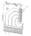
图1示出了可以根据本发明进行改善的示例性连接器系统。在图1的示例中,电连接器是两件式电连接器,其适合于将印刷电路板以直角连接到底板。该连接器包括底板连接器110和适合于与底板连接器110配合的子卡连接器120。Figure 1 shows an exemplary connector system that can be improved in accordance with the present invention. In the example of FIG. 1 , the electrical connector is a two-piece electrical connector suitable for connecting a printed circuit board to a chassis at a right angle. The connectors include a
底板连接器110包括多个信号导体,其通常以列进行布置。信号导体保持在壳体116中,壳体116典型地由塑料或者其他适当的材料模制而成。每个信号导体包括接触尾部112和配合部分114。在使用中,接触尾部112可以附连到底板内的导电走线。在所示的示例性实施例中,接触尾部112是压力配合式接触尾部,该尾部插入到底板中的孔内。压力配合式接触尾部与底板内的导电镀层形成连接,该导电镀层又连接到底板内的走线。其他形式的接触尾部是已知的,并且本发明不限于任何具体形式。例如,可以利用表面安装或者压力安装的接触尾部构造电连接器。
在图1的示例中,信号导体的配合部分114被成形为叶片形。底板连接器110中的信号导体的配合部分114被定位为与子卡连接器120中的信号导体的配合部分相配合。在该示例中,底板连接器110的配合部分114与子卡连接器120的配合部分126相配合,从而形成可分离的配合接口,信号可以通过该配合接口传送。In the example of FIG. 1 , the
子卡连接器120内的信号导体保持在壳体136内,壳体136可由塑料或者其他适当的材料形成。接触尾部124从壳体延伸并且被定位为用于附连到子卡。在图1的示例中,子卡连接器120的接触尾部124是与接触尾部112相似的压力配合式接触尾部。然而,可以使用任何适当的附连机构。The signal conductors within
在所示的非限制性示例中,子卡连接器120由片状件122形成。为了简单起见,图1中示出了单个片状件122。诸如片状件122的片状件可被形成为子组件,每个子组件包含用于一个连接器列的信号导体。片状件可以一起保持在支撑结构中,诸如金属加强件130。每个片状件在其壳体中包括附连特征128,其可以将片状件122附连到加强件130。In the non-limiting example shown, the
加强件130是可用于形成连接器的支撑结构的一个示例,但是本发明不限于与具有加强件的连接器结合使用。例如,支撑结构可设置为采用绝缘壳体、梳子、和其他形状的金属构件的形式。而且,在某些实施例中,支撑部件可被完全省略。片状件可以通过粘合剂或者其他装置保持在一起。作为另一示例,连接器可被形成为整体式壳体,信号导体插入到该整体式壳体中。The
当组装到连接器时,片状件的接触尾部124大致从子卡连接器120的绝缘壳体的正面延伸。在使用中,使该正面压靠子卡(未示出)的表面,从而在接触尾部124和子卡内的信号走线之间形成连接。相似地,底板连接器110的接触尾部112从壳体116的正面延伸。使该正面压靠底板(未示出)的表面,从而允许接触尾部112连接到底板内的走线。这样,信号可以从子卡通过子卡120中的信号导体传递到底板连接器110的信号导体内,其中该信号可以连接到底板内的走线。The
当需要时,可以将屏蔽构件放置在底板连接器的信号导体列和子卡连接器之间。同样地,这些屏蔽可以包括接触部分,其允许电流通过子卡连接器120和底板连接器110之间的配合接口。该屏蔽构件可以连接到子卡或者底板内的接地平面,从而提供通过连接器的接地平面,其减少了信号导体之间的串扰并且还可用于控制信号导体的阻抗。When desired, a shielding member may be placed between the signal conductor columns of the backplane connector and the daughter card connector. Likewise, these shields may include contact portions that allow electrical current to pass through the mating interface between
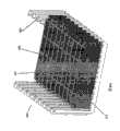
根据本发明的一个非限制性方面,图2A和2B中示出了可以减少串扰的布置。图2A示出了片状件122’,其包括互连系统中的用于减少串扰的特征。配合部分710被成形为配合在底板连接器210的壳体216内。配合部分710包括片状件122’内的信号导体的配合部分712,其接合底板连接器110内的信号导体的配合部分114(图1)。在所示的实施例中,配合部分712成对地定位。然而,其他构造也在本发明的范围内。According to one non-limiting aspect of the invention, arrangements that may reduce crosstalk are shown in Figures 2A and 2B. Figure 2A shows a flap 122' that includes features in the interconnection system to reduce crosstalk. The
片状件122’可形成有在配合部分710内的信号导体之间的空腔720。空腔720可被成形为容纳有损插入件722。有损插入件722可由如下材料制成或者包括如下材料,该材料通常被称为有损导体或有损电介质,其通常被称为“电有损材料”。电有损材料可由如下材料形成,该材料通常被认为是导体,但是在有利的频率范围上是较差的导体,并且包含充分分散的不提供高导电性的颗粒和区域,或者另外被制备为具有如下属性,即在有利的频率范围上导致较弱的体积导电性。电有损材料典型地具有约1西门子/米至约6.1×107西门子/米,优选地约1西门子/米至约1×107西门子/米,最优选地约1西门子/米至约30000西门子/米的导电率。The
电有损材料可以是部分导电的材料,诸如具有1Ω/平方米至106Ω/平方米的表面电阻率。在某些实施例中,电有损材料具有约1Ω/平方米至约103Ω/平方米的表面电阻率。在其他的实施例中,电有损材料具有约10Ω/平方米至约100Ω/平方米的表面电阻率。作为具体示例,该材料可以具有约20Ω/平方米至约40Ω/平方米的表面电阻率。The electrically lossy material may be a partially conductive material, such as having a surface resistivity of 1 Ω/square to 106 Ω/square. In certain embodiments, the electrically lossy material has a surface resistivity of about 1 Ω/square to about 103 Ω/square. In other embodiments, the electrically lossy material has a surface resistivity of about 10 Ω/square to about 100 Ω/square. As a specific example, the material may have a surface resistivity of about 20 Ω/square to about 40 Ω/square.
在某些实施例中,通过将包含导电颗粒的填料添加到粘合剂而形成电有损材料。可用作用于形成电有损材料的导电颗粒的示例包括被形成为纤维的碳或石墨、薄片、镍-石墨粉末或者其他颗粒。采用粉末、薄片、纤维、不锈钢纤维、或者其他颗粒的形式的金属也可用于提供适当的电气有损性能。另外地或者可选地,可以使用填料的组合。例如,可以使用镀金属的碳颗粒。银和镍是用于纤维的合适的金属镀层。涂覆颗粒可以单独使用或者与其他填料组合使用。也可以使用纳米管材料。也可以使用材料的混合物,并且其在本发明的范围内。In certain embodiments, the electrically lossy material is formed by adding fillers comprising conductive particles to the binder. Examples of conductive particles that may be used to form electrically lossy materials include carbon or graphite formed into fibers, flakes, nickel-graphite powder, or other particles. Metals in the form of powders, flakes, fibers, stainless steel fibers, or other particles may also be used to provide suitable electrical lossy properties. Additionally or alternatively, combinations of fillers may be used. For example, metallized carbon particles may be used. Silver and nickel are suitable metal coatings for fibers. Coated particles can be used alone or in combination with other fillers. Nanotube materials can also be used. Mixtures of materials may also be used and are within the scope of the present invention.
优选地,填料将具有足够的体积百分比,以允许产生从颗粒到颗粒的导电路径。例如,在使用金属纤维时,该纤维的体积可为约3%至约40%。填料的量可以影响材料的导电性能。在另一实施例中,粘合剂可装填有占约10%至约80%的体积的导电填料。该装填可以超过约30%的体积。作为另一示例,可以装填占约40%至约60%的体积的导电填料。Preferably, the filler will be of sufficient volume percentage to allow a conductive path from particle to particle to be created. For example, when metal fibers are used, the fibers may comprise from about 3% to about 40% by volume. The amount of filler can affect the conductive properties of the material. In another embodiment, the adhesive may be loaded with a conductive filler comprising from about 10% to about 80% by volume. This packing can exceed about 30% by volume. As another example, about 40% to about 60% by volume of conductive filler may be loaded.
在使用纤维填料时,纤维可以具有约0.5mm至约15mm的长度。作为具体示例,该长度可以是约3mm至约11mm。在一个示例性实施例中,纤维长度是约3mm至约8mm。When using fibrous fillers, the fibers may have a length of from about 0.5 mm to about 15 mm. As a specific example, the length may be about 3 mm to about 11 mm. In an exemplary embodiment, the fiber length is from about 3mm to about 8mm.
在示例性实施例中,纤维填料具有高的长宽比(长度与宽度的比)。在该实施例中,纤维优选地具有超过约10,更优选地超过约100的长宽比。在另一实施例中,塑料树脂用作用于保持镀镍石墨薄片的粘合剂。作为具体(非限制性)示例,有损导电材料可以是约30%的涂镍纤维、约40%的LCP(液晶聚合物)和约30%的PPS(聚苯硫醚)。In an exemplary embodiment, the fibrous filler has a high aspect ratio (ratio of length to width). In this embodiment, the fibers preferably have an aspect ratio in excess of about 10, more preferably in excess of about 100. In another embodiment, a plastic resin is used as a binder for holding the nickel-coated graphite flakes. As a specific (non-limiting) example, the lossy conductive material may be about 30% nickel-coated fibers, about 40% LCP (liquid crystal polymer), and about 30% PPS (polyphenylene sulfide).
填充材料可以商业购买,诸如Ticona销售的商标为
有损插入件722可以以任何适当的方式形成。例如,可以使用横截面与有损插入件722所需的横截面相同的棒材挤压填充粘合剂。该棒材可被切割为片段,该片段具有有损插入件722所需的厚度。然后可以将该片段插入到空腔720中。通过干涉配合或者通过使用粘合剂或者其他的固定装置,可将该插入件维持在空腔722中。作为可选实施例,可以将如上文所述地填充的未固化材料插入到空腔720中并且在适当的位置固化。
图2B表示具有导电插入件722处于适当位置的片状件122’。如该视图所示,导电插入件722使信号导体对的配合部分712分离。片状件122’可以包括屏蔽构件,其通常平行于片状件122’内的信号导体。在存在屏蔽构件的情况下,有损插入件722可以电气耦合到屏蔽构件并且形成直接电气连接。可以使用导电环氧树脂或者其他导电胶粘剂实现耦合,以将有损插入件固定到屏蔽构件。可选地,可以使有损插入件722压靠屏蔽构件而实现有损插入件722和屏蔽构件之间的电气耦合。有损插入件722同屏蔽构件的紧密物理接近可以实现屏蔽构件和有损插入件之间的电容耦合。可选地,如果有损插入件722在足够压力地压靠屏蔽构件的情况下维持在片状件122’内,则可以形成直接连接。Figure 2B shows the tab 122' with the
然而,不需要有损插入件722和屏蔽构件之间的电气耦合。有损插入件722可以在没有屏蔽构件的连接器中使用,以减少互连系统的配合部分710中的串扰。根据本发明的另一方面,每个片状件可以包括与本申请在同一日期提交的共同未决的律师卷号124315-00462中描述的一个或多个特征,该专利申请要求临时专利申请序列号No.60/695,308的优先权,其内容在此处整体并入作为参考。在一个非限制性的实施例中,片状件被形成为具有两个壳体部分,即保持和分离导电信号对的第一绝缘部分和用于提供所需屏蔽的第二导电部分。片状件中的导电接地带可以在与导电信号带相同的平面中形成,并且第二壳体部分(例如,壳体的导电部分)连接到(例如,模制的)接地带,并且与信号带适当地隔开。片状件还可被形成为具有在一个片状件的导电带(例如,信号带)之间的空气间隙,并且相邻于片状件的导电壳体在不显著牺牲信号强度的情况下进一步减少了电气噪声或其他损耗(例如,串扰)。该现象的出现至少部分是由于空气间隙提供了信号对的一个信号带和该信号对的另一信号带之间的优选的信号通讯或耦合,而屏蔽用于限制信号对之间的串扰。However, there is no need to compromise the electrical coupling between the
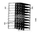
根据本发明的另一方面,可以如图3A所示地形成连接器(诸如上文并入的申请所述,其律师卷号为No.124315-00462)。如图3A所示,多件式电连接器200可以包括底板连接器205和子卡连接器210,子卡连接器210包括前壳体206。底板连接器205包括底板外罩202和多个触点212,这里多个触点212被布置为差分信号对的阵列。在所示的非限制性实施例中,触点可以连接到成对分组的印刷电路板,诸如可以适用于承载差分信号的印刷电路板。每对印刷电路板可以通过接地的触点与一个相邻的印刷电路板对隔开。信号触点212的单端构造也在本发明的范围内,其中导体未成对地分组。According to another aspect of the present invention, a connector may be formed as shown in FIG. 3A (such as described in the above-incorporated application, Attorney Docket No. 124315-00462). As shown in FIG. 3A , the multi-piece electrical connector 200 may include a backplane connector 205 and a daughter card connector 210 including a
在所示实施例中,底板外罩202由介电材料模制而成。该材料的示例是液晶聚合物(LCP)、聚苯硫醚(PPS)、高温尼龙或者聚丙烯(PPO)。由于本发明在这一点上不受限制,也可以使用其他适当的材料。所有这些材料也适合于用作在制造根据本发明的连接器中使用的粘合剂材料。In the illustrated embodiment, the backplane housing 202 is molded from a dielectric material. Examples of such materials are liquid crystal polymer (LCP), polyphenylene sulfide (PPS), high temperature nylon or polypropylene (PPO). Other suitable materials may also be used, as the invention is not limited in this regard. All these materials are also suitable as adhesive material used in the manufacture of the connector according to the invention.
触点212延伸通过底板外罩202的底面204,从而在外罩202的底面204的上面和下面提供接触区域。这里,外罩面板204上面的触点212的接触区域适合于配合到子卡连接器210中的触点。在所示实施例中,由于本发明在这一点上不受限制,故尽管也可以使用其他适当的接触构造,但是配合接触区域采用叶片接触的形式。The contacts 212 extend through the bottom surface 204 of the chassis housing 202 to provide contact areas above and below the bottom surface 204 of the housing 202 . Here, the contact areas of the contacts 212 on the housing panel 204 are adapted to mate to contacts in the daughter card connector 210 . In the illustrated embodiment, the mating contact areas take the form of blade contacts, although other suitable contact configurations may be used, as the invention is not limited in this respect.
触点212的尾部部分211在外罩底面204下面延伸并且适合于配合到印刷电路板。这里,尾部部分采用压力配合的形式,例如,“针眼”屈服接触。然而,由于本发明在这一点上不受限制,故其他构造也是适当的,诸如表面安装元件、弹簧触点、可焊接引脚等。在一个实施例中,子卡连接器210可以包括前壳体206,其配合在底板连接器205的侧壁208之间。Tail portions 211 of contacts 212 extend below housing bottom surface 204 and are adapted to fit to a printed circuit board. Here, the tail section takes the form of a force fit, for example, an "eye of the needle" yielding contact. However, as the invention is not limited in this respect, other configurations are suitable, such as surface mount components, spring contacts, solderable pins, and the like. In one embodiment, daughtercard connector 210 may include a
底板外罩202还可以包括侧壁208,其沿底板外罩202的相对侧的长度延伸。侧壁208包括凹槽218,其沿侧壁208的内表面垂直延伸。凹槽218用于经由配合凸起207将前壳体206引导至外罩202中的适当位置。在某些实施例中,可以设置多个屏蔽(未示出),并且该屏蔽可以与侧壁208平行地延伸并且可以位于信号触点对202的行之间。在单端构造中,多个屏蔽板可以位于信号触点对212的行之间。然而,其他的屏蔽构造也在本发明的范围内,包括在外罩的壁之间延伸的屏蔽、横向于侧壁208的屏蔽或者完全省略屏蔽。如果使用屏蔽,则屏蔽可由金属片模压而成,并且可被成形为板或者叶片,或者具有任何其他的所需形状。The floor housing 202 may also include side walls 208 that extend along the length of opposite sides of the floor housing 202 . The sidewall 208 includes a groove 218 extending vertically along the inner surface of the sidewall 208 . The grooves 218 are used to guide the
如果使用屏蔽,则每个屏蔽可以包括一个或多个尾部部分,其延伸通过外罩底面204。由于具有信号触点的尾部,故屏蔽可以具有被形成为“针眼”屈服触点的尾部部分,其压力配合到底板内。然而,由于本发明在这一点上不受限制,故其他的配置也是适当的,诸如表面安装元件、弹簧触点、可焊接引脚等。If shields are used, each shield may include one or more tail portions that extend through housing bottom surface 204 . As with the tails of the signal contacts, the shield may have tail portions formed as "eye of the needle" yield contacts that are press fit into the chassis. However, as the invention is not limited in this respect, other configurations are suitable, such as surface mount components, spring contacts, solderable pins, and the like.
如上所述,子卡连接器210包括多个模块或者片状件220,其由支架230支撑。每个片状件220包括插入到支架中的孔隙231的特征,以使每个片状件220相互定位并且进一步防止片状件220的旋转。当然,本发明在这一点上不受限制,并且不需要使用支架。而且,由于可以使用其他的适当位置,故尽管支架被示出为附连到多个片状件的上部和侧部,但是本发明在这一点上不受限制。As mentioned above, the daughter card connector 210 includes a plurality of modules or blades 220 supported by brackets 230 . Each flap 220 includes a feature of an aperture 231 that is inserted into the bracket to position each flap 220 relative to one another and further prevent rotation of the flap 220 . Of course, the invention is not limited in this regard and does not require the use of brackets. Also, although the brackets are shown attached to the upper and sides of the plurality of flaps, the invention is not limited in this regard, as other suitable locations may be used.
仅出于示例性的目的,子卡连接器210示出为具有三个片状件220,每个片状件220具有信号导体对,其由接地带围绕或者另外与该接地带相邻。然而,由于片状件的数量和每个片状件中的信号导体和屏蔽带的数量可以按照需要改变,故本发明在这一点上不受限制。每个片状件沿狭槽209插入到前壳体206内,使得配合接触部分(224、226,图3B)被插入到空腔213内,以便定位成当子卡连接器和底板连接相配合时实现同底板连接器205的信号触点212的电气连接。For exemplary purposes only, daughtercard connector 210 is shown as having three blades 220 each having a pair of signal conductors surrounded by or otherwise adjacent to a ground strap. However, the invention is not limited in this regard, as the number of wafers and the number of signal conductors and shielding straps in each wafer can vary as desired. Each tab is inserted into the
现在参考图3B,示出了子卡连接器的单个片状件。片状件220包括两个部分的壳体232,其在信号带和接地带的引导框架(也称为接地带)周围形成。在一个实施例中,通过在包含导电带的引导框架周围模制第一绝缘部分,形成片状件220,其中导电带将形成连接器中的信号导体和接地导体。可执行第二模制操作,以在被模制为第一绝缘部分的引导框架的子组件周围,模制壳体的第二导电部分。该第二部分可由填充有导电填料的粘合剂形成。该填料可以形成上述的有损导电部分,或者可以是更加导电的和/或更少损耗的。Referring now to FIG. 3B , a single blade of a daughter card connector is shown. The flap 220 includes a two-
多个信号触点尾部228和多个接地触点尾部222从每个片状件220的第一边缘延伸,并且从引导框架的相应带的第一边缘延伸。在板到板的连接器的示例中,这些触点尾部将信号带和接地带连接到印刷电路板。在示例性实施例中,每个片状件220上的多个接地触点尾部222和信号触点尾部228布置在单个平面中,尽管本发明在这一点上不受限制。而且,在另一示例性实施例中,每个片状件220上的多个信号带和接地带布置在单个平面中,尽管本发明在这一点上不受限制。A plurality of
这里,信号触点尾部228和接地触点尾部222采用压力配合式“针眼”构造的形式,其被按压到位于印刷电路板(未示出)中的镀覆通孔中。在该示例性实施例中,信号触点尾部228可以连接到印刷电路板上的信号走线,并且接地触点尾部222可以连接到印刷电路板中的接地平面。在所示实施例中,信号触点尾部228被构造为提供差分信号并且成对布置。Here, the
信号触点的配合接触部分224位于每个片状件220的第二边缘附近,并且与底板连接器205的信号触点212相配合。这里,配合接触部分224被设置为采用双梁的形式,以与底板信号触点212的叶片接触端相配合。在所示的实施例中,暴露配合接触部分,用于插入到前壳体206内。然而,本发明在这一点上不受限制,并且配合接触区域可以放置在电介质壳体232中的开口内以保护触点,如上文参考图2A和2B的实施例所示和所述。The
子卡连接器的配合正面中的开口,允许触点212接合子卡连接器中的相应触点,用于子板和底板信号触点的配合,不论该开口是由图3A所示的前壳体206形成或者是由图2A和2B所示的独立片状件上的壳体形成。由于本发明在这一点上不受限制,故可以使用其他适当的触点构造。Openings in the mating front of the daughter card connector that allow contacts 212 to engage corresponding contacts in the daughter card connector for mating daughterboard and backplane signal contacts, regardless of whether the opening is made of the front housing as shown in FIG. 3A The
在双梁式触点对224之间并且在片状件的第二边缘附近设置接地触点226。接地触点可以连接到子卡接地带,并且可以接合底板连接器中的接地触点的配合部分,如果采用该接地触点,则其可以是底板屏蔽板。应当认识到的是,由于可以使用其他适当的触点,故本发明不限于所示屏蔽触点的具体形状。因此,所示触点仅是示例性的,而并非为限制性的。A
现在转到图3C,现在将描述前壳体206的实施例的其他特征。如图所示,前壳体206为大致U形体并且包括上述的空腔213,其允许片状件的尾部与底板壳体的叶片相连接。前壳体典型地由适当的材料模制而成,诸如上述的任何非导电材料。在一个实施例中,前壳体是由热塑性粘合剂模制而成,该粘合剂中引入了非导电纤维用于增加强度、空间稳定性并且减少所使用的高价格粘合剂的数量。玻璃纤维是典型的,装填量为约30%的体积。Turning now to FIG. 3C , additional features of the embodiment of the
根据本发明的一个方面,为了减少触点224与底板触点212相配合处的串扰,前壳体206具有屏蔽。该屏蔽可以代替设置底板连接器205和/或子卡连接器210中的任何屏蔽或者添加到该屏蔽。在一个实施例中,在前壳体中的适当位置设置屏蔽板300。如图所示,屏蔽板300可以放置在前壳体206中的如下位置处,即使得该屏蔽板300位于相邻的孔隙列213之间。然而,由于本发明在这一方面不受限制,故可以使用用于减少串扰的其他位置。在一个实施例中,在将片状件插入到前壳体206内时,每个屏蔽板可以与接触部分列224隔开,以便于将信号导体的阻抗维持为小于约500Ω。在一个实施例中,在将片状件插入到前壳体206内时,屏蔽板与配合接触部分224隔开,以便于将信号导体的阻抗维持为小于约100Ω。在又一实施例中,在将片状件插入到前壳体206内时,屏蔽板与触点尾部224隔开,以便于将信号导体的阻抗维持为小于约50Ω。According to one aspect of the invention, to reduce crosstalk where the
由于本发明在这一点不受限制,故该屏蔽板可以以任何适当的方式放置在前壳体内。在一个实施例中,前壳体形成有狭槽310,其可以在前壳体的模制期间形成。当然,由于本发明在这一点不受限制,故可以使用用于形成狭槽的其他适当的制造技术,诸如在形成前壳体之后加工该狭槽。狭槽310的尺寸可形成为容纳板300。该狭槽的宽度可使得可以实现前壳体和屏蔽板之间的压力配合,由此牢固地将该板保持在适当的位置。由于本发明在这一点不受限制,故可以使用用于将该板保持在适当位置的其他的适当技术,诸如利用粘合剂、紧固件等。As the invention is not limited in this regard, the shield may be placed within the front housing in any suitable manner. In one embodiment, the front case is formed with a
在可选实施例中,屏蔽板310可模制有壳体,使得在完成模制操作时该屏蔽板被牢固地保持在壳体内。In an alternative embodiment, the
该屏蔽板被构造为形成与片状件的接地带的电气连接。在一个实施例中,屏蔽板包括突片312,该突片312可被偏置以在将片状件插入在前壳体中时与片状件的触点尾部226相接合。The shielding plate is configured to form an electrical connection with the ground strap of the blade. In one embodiment, the shield plate includes
在一个实施例中,屏蔽板由金属形成,然而,本发明在这一点不受限制,可以使用适当的导电塑料,诸如上述的有损材料。在一个实施例中,由于本发明在这一点不受限制,故可以通过模压金属板形成该屏蔽板,尽管可以铸造、加工、或者通过其他的适当方法形成该板。而且,突片312可以在模压操作期间形成。In one embodiment, the shield is formed from metal, however, the invention is not limited in this regard and suitable conductive plastics such as the lossy materials described above may be used. In one embodiment, the shield may be formed by stamped sheet metal, although the plate may be cast, machined, or formed by other suitable means, as the invention is not limited in this regard. Also,
图4A和4B表示前壳体206的可选实施例,其中图4A表示完成的前壳体的组装透视图。前壳体部分400被形成为不具有屏蔽构件300。在前壳体400中通过使用电有损材料减少串扰。如上所述,可以利用在用作粘合剂的绝缘材料中的导电填料,形成电有损材料。在一个实施例中,在两次注模操作中模制电有损材料和绝缘材料,以形成具有绝缘片段和有损片段的完整壳体。如图4B所示,其是由实线表示的有损片段的视图,首先模制有损材料,然后在壳体的有损片段上模制前壳体的剩余部分(例如,绝缘片段),该剩余部分由较浅的虚线表示。当然,本发明在这一点不受限制,可以执行其他适当的模制操作,以制造具有有损片段的前壳体。而且,尽管有损材料被形成为整体式有损片段,但是本发明不限于此,可以在前壳体中形成多个分离的有损片段。Figures 4A and 4B show an alternative embodiment of the
有损片段可定位绝缘壳体内处于需要抑制串扰的位置。在图4A和4B所示的实施例中,前壳体400形成有绝缘材料的侧壁407。绝缘材料还定位为使得每个空腔413在可能接触该导体的任何片段中衬有绝缘材料,该空腔413容纳用于承载信号的片状件220内的导体的配合接触部分224。电有损材料可被定位在配合接触部分列之间的区域中,诸如区域420。如图所示,区域420延伸到前壳体的底部。Lossy segments can be positioned within the insulating housing at locations where crosstalk suppression is desired. In the embodiment shown in FIGS. 4A and 4B , the
此外,前壳体400可模制有在空腔413之间的有损材料。在图4A和4B所示的实施例中,连接器被构造为用于差分信号,使得配合接触部分采取成对的形式。因此,前壳体部分400包括垂直于空腔对413之间的列延伸的有损导电材料422的区域,该空腔对413适合于容纳承载一个差分信号的两个导体的配合接触部分。如图所示,区域422仅部分地朝向前壳体的底部延伸,并且其延伸程度小于区域420的延伸程度。当然,本发明在这一点不受限制,该区域可以延伸相同的量,或者区域422可以比区域420进一步朝向前壳体的底部延伸。Additionally, the
可选择前壳体部分400内包含的有损材料的量和程度,以在没有不理想地使传送通过前壳体部分400的信号衰减的情况下将串扰减少到所需的水平。在相邻列之间的部分420可用于代替或者添加到垂直于该列延伸的部分422。此外,可在前壳体部分中使用有损材料,以代替或添加到诸如图3C所示的屏蔽构件。The amount and extent of lossy material contained within the
因此,通过对本发明的至少一个实施例的数个方面的描述,应当认识到的是,本领域的技术人员将易于想到多种改变、修改、和改进。Having thus described several aspects of at least one embodiment of this invention, it is to be appreciated various alterations, modifications, and improvements will readily occur to those skilled in the art.
例如,本发明是结合底板/子卡连接器系统进行说明。本发明的用途并非限于此。本发明可以并入到诸如被典型地描述为中间面连接器、堆叠连接器、夹层连接器的连接器中,或者并入到任何其他的互连系统中。For example, the invention is described in connection with a backplane/daughtercard connector system. The use of the present invention is not limited thereto. The present invention may be incorporated into connectors such as those typically described as midplane connectors, stacking connectors, mezzanine connectors, or into any other interconnection system.
作为另一示例,信号导体被描述为成行和列布置。除非另外清楚地指出,否则术语“行”或“列”并非指明具体的取向。而且,某种导体被限定为“信号导体”。尽管该导体适于承载高速电气信号,但是并非要求以该方式使用所有的信号导体。例如,某些信号导体可以接地,或者在连接器被安装在电子系统中时简单地不被使用。As another example, signal conductors are described as being arranged in rows and columns. The terms "row" or "column" do not denote a particular orientation unless clearly stated otherwise. Also, certain conductors are defined as "signal conductors". Although the conductors are suitable for carrying high speed electrical signals, not all signal conductors are required to be used in this manner. For example, certain signal conductors may be grounded, or simply not used when the connector is installed in an electronic system.
相似地,使用了术语“前壳体”。除非清楚地指出,否则术语“前”不需要应用于任何具体取向。例如,在夹层连接器中,“前壳体”可被取向为向上的方向,并且还可被描述为顶壳体。Similarly, the term "front housing" is used. The term "front" need not apply to any particular orientation unless clearly indicated otherwise. For example, in a mezzanine connector, a "front housing" may be oriented in an upward direction, and may also be described as a top housing.
而且,尽管该列都被示出为具有相同的信号导体数量,但是本发明不限于用于具有矩形导体阵列的互连系统中。而且信号导体也没有必要占据列中的每个位置。Also, although the columns are all shown as having the same number of signal conductors, the invention is not limited to use in interconnect systems having rectangular conductor arrays. Also, it is not necessary for signal conductors to occupy every position in the column.
同样地,某些导体被描述为接地导体或者参考导体。该连接器适合于形成接地连接,但是不需要以该方式使用。Likewise, certain conductors are described as ground conductors or reference conductors. This connector is suitable for making a ground connection, but need not be used in this manner.
而且,此处使用的术语“地”用于表示参考电位。例如,地可以是正的或者负的电源,并且不需要限于地球地。Also, the term "ground" as used herein is used to denote a reference potential. For example, ground can be a positive or negative power supply and need not be limited to earth ground.
该改变、修改、和改进应为本公开内容的一部分,并且应在本发明的精神和范围内。因此,前面的描述和附图应仅作为示例。Such alterations, modifications, and improvements are intended to be part of this disclosure, and are intended to be within the spirit and scope of the invention. Accordingly, the foregoing description and drawings should be taken by way of example only.
Claims (27)
Translated fromChinesePriority Applications (1)
| Application Number | Priority Date | Filing Date | Title |
|---|---|---|---|
| CN201210249710.9ACN102882097B (en) | 2005-06-30 | 2006-06-30 | The connector with improved shielding in cooperation contact area |
Applications Claiming Priority (5)
| Application Number | Priority Date | Filing Date | Title |
|---|---|---|---|
| US69526405P | 2005-06-30 | 2005-06-30 | |
| US60/695,264 | 2005-06-30 | ||
| US11/476,758 | 2006-06-29 | ||
| US11/476,758US8083553B2 (en) | 2005-06-30 | 2006-06-29 | Connector with improved shielding in mating contact region |
| PCT/US2006/025562WO2007005597A2 (en) | 2005-06-30 | 2006-06-30 | Connector with improved shielding in mating contact region |
Related Child Applications (1)
| Application Number | Title | Priority Date | Filing Date |
|---|---|---|---|
| CN201210249710.9ADivisionCN102882097B (en) | 2005-06-30 | 2006-06-30 | The connector with improved shielding in cooperation contact area |
Publications (2)
| Publication Number | Publication Date |
|---|---|
| CN101258649Atrue CN101258649A (en) | 2008-09-03 |
| CN101258649B CN101258649B (en) | 2012-09-05 |
Family
ID=37605029
Family Applications (2)
| Application Number | Title | Priority Date | Filing Date |
|---|---|---|---|
| CN2006800239976AActiveCN101258649B (en) | 2005-06-30 | 2006-06-30 | Connectors with improved shielding in the mating contact area |
| CN201210249710.9AActiveCN102882097B (en) | 2005-06-30 | 2006-06-30 | The connector with improved shielding in cooperation contact area |
Family Applications After (1)
| Application Number | Title | Priority Date | Filing Date |
|---|---|---|---|
| CN201210249710.9AActiveCN102882097B (en) | 2005-06-30 | 2006-06-30 | The connector with improved shielding in cooperation contact area |
Country Status (6)
| Country | Link |
|---|---|
| US (2) | US8083553B2 (en) |
| EP (1) | EP1897181A4 (en) |
| JP (1) | JP2008545249A (en) |
| CN (2) | CN101258649B (en) |
| IL (1) | IL188368A0 (en) |
| WO (1) | WO2007005597A2 (en) |
Cited By (15)
| Publication number | Priority date | Publication date | Assignee | Title |
|---|---|---|---|---|
| CN102148444A (en)* | 2010-12-08 | 2011-08-10 | 深圳格力浦电子有限公司 | High-speed signal connector socket structure for printed board and backboard |
| CN103117486A (en)* | 2011-07-13 | 2013-05-22 | 泰科电子公司 | Electrical connector assembly for interconnecting an electronic module and an electrical component |
| CN104737384A (en)* | 2012-10-18 | 2015-06-24 | 山一电机株式会社 | Receptacle connector, plug connector and electrical connector provided with receptacle connector and plug connector |
| CN105071072A (en)* | 2015-08-25 | 2015-11-18 | 安费诺商用电子产品(成都)有限公司 | Orthogonal backplane connector |
| CN106025719A (en)* | 2015-03-27 | 2016-10-12 | 泰科电子公司 | Electrical connector and interconnection system having resonance control |
| CN107046201A (en)* | 2015-12-14 | 2017-08-15 | 泰科电子公司 | Include the electric connector of lossy distance piece |
| CN107123902A (en)* | 2016-02-25 | 2017-09-01 | 泰连公司 | Grounding contact module for contact module stacked body |
| CN108429028A (en)* | 2017-02-13 | 2018-08-21 | 泰连公司 | Inhibit the electric connector of electric resonance |
| CN110994227A (en)* | 2019-06-06 | 2020-04-10 | 富鼎精密工业(郑州)有限公司 | Electrical connector |
| CN110994284A (en)* | 2019-06-06 | 2020-04-10 | 富鼎精密工业(郑州)有限公司 | Electrical connector |
| US11522310B2 (en) | 2012-08-22 | 2022-12-06 | Amphenol Corporation | High-frequency electrical connector |
| US11539171B2 (en) | 2016-08-23 | 2022-12-27 | Amphenol Corporation | Connector configurable for high performance |
| US11715914B2 (en) | 2014-01-22 | 2023-08-01 | Amphenol Corporation | High speed, high density electrical connector with shielded signal paths |
| US11942716B2 (en) | 2020-09-22 | 2024-03-26 | Amphenol Commercial Products (Chengdu) Co., Ltd. | High speed electrical connector |
| US12074398B2 (en) | 2020-01-27 | 2024-08-27 | Fci Usa Llc | High speed connector |
Families Citing this family (122)
| Publication number | Priority date | Publication date | Assignee | Title |
|---|---|---|---|---|
| US7163421B1 (en)* | 2005-06-30 | 2007-01-16 | Amphenol Corporation | High speed high density electrical connector |
| US8083553B2 (en)* | 2005-06-30 | 2011-12-27 | Amphenol Corporation | Connector with improved shielding in mating contact region |
| US20090291593A1 (en) | 2005-06-30 | 2009-11-26 | Prescott Atkinson | High frequency broadside-coupled electrical connector |
| DE102006011624A1 (en)* | 2006-03-10 | 2007-09-13 | Carl Zeiss Meditec Ag | Device and method for the defined alignment of an eye |
| US7632149B2 (en)* | 2006-06-30 | 2009-12-15 | Molex Incorporated | Differential pair connector featuring reduced crosstalk |
| US7722400B2 (en)* | 2006-06-30 | 2010-05-25 | Molex Incorporated | Differential pair electrical connector having crosstalk shield tabs |
| US7497736B2 (en) | 2006-12-19 | 2009-03-03 | Fci Americas Technology, Inc. | Shieldless, high-speed, low-cross-talk electrical connector |
| US7985097B2 (en)* | 2006-12-20 | 2011-07-26 | Amphenol Corporation | Electrical connector assembly |
| US7794240B2 (en)* | 2007-04-04 | 2010-09-14 | Amphenol Corporation | Electrical connector with complementary conductive elements |
| US7722401B2 (en) | 2007-04-04 | 2010-05-25 | Amphenol Corporation | Differential electrical connector with skew control |
| WO2008124101A2 (en)* | 2007-04-04 | 2008-10-16 | Amphenol Corporation | Electrical connector lead frame |
| TWM322090U (en) | 2007-05-11 | 2007-11-11 | Chief Land Electronic Co Ltd | Ground terminal capable of preventing noise |
| US7651337B2 (en)* | 2007-08-03 | 2010-01-26 | Amphenol Corporation | Electrical connector with divider shields to minimize crosstalk |
| EP2240980A2 (en) | 2008-01-17 | 2010-10-20 | Amphenol Corporation | Electrical connector assembly |
| US8764464B2 (en) | 2008-02-29 | 2014-07-01 | Fci Americas Technology Llc | Cross talk reduction for high speed electrical connectors |
| US8298015B2 (en) | 2008-10-10 | 2012-10-30 | Amphenol Corporation | Electrical connector assembly with improved shield and shield coupling |
| US8172614B2 (en) | 2009-02-04 | 2012-05-08 | Amphenol Corporation | Differential electrical connector with improved skew control |
| US9277649B2 (en) | 2009-02-26 | 2016-03-01 | Fci Americas Technology Llc | Cross talk reduction for high-speed electrical connectors |
| US8366485B2 (en) | 2009-03-19 | 2013-02-05 | Fci Americas Technology Llc | Electrical connector having ribbed ground plate |
| WO2011031311A2 (en) | 2009-09-09 | 2011-03-17 | Amphenol Corporation | Compressive contact for high speed electrical connector |
| CN102906947B (en) | 2009-11-13 | 2016-04-13 | 安费诺有限公司 | The connector controlled with normal mode reactance of high-performance, small-shape factor |
| US8616919B2 (en)* | 2009-11-13 | 2013-12-31 | Fci Americas Technology Llc | Attachment system for electrical connector |
| US8515040B2 (en) | 2009-12-03 | 2013-08-20 | Alcatel Lucent | Geospatial telephony system |
| JP2011159470A (en)* | 2010-01-29 | 2011-08-18 | Fujitsu Component Ltd | Male connector, female connector, and connector |
| US8740647B1 (en)* | 2010-02-02 | 2014-06-03 | Arris Enterprises, Inc. | Reduced crosstalk in a multi-channel conductive body connector |
| CN102859805B (en) | 2010-02-24 | 2016-07-06 | 安费诺有限公司 | High bandwidth connector |
| CN107069274B (en) | 2010-05-07 | 2020-08-18 | 安费诺有限公司 | High performance cable connector |
| WO2012047619A1 (en)* | 2010-09-27 | 2012-04-12 | Fci | Electrical connector having commoned ground shields |
| WO2012106554A2 (en) | 2011-02-02 | 2012-08-09 | Amphenol Corporation | Mezzanine connector |
| US8888529B2 (en) | 2011-02-18 | 2014-11-18 | Fci Americas Technology Llc | Electrical connector having common ground shield |
| JP5904573B2 (en)* | 2011-08-19 | 2016-04-13 | 富士通コンポーネント株式会社 | connector |
| CN103931057B (en) | 2011-10-17 | 2017-05-17 | 安费诺有限公司 | Electrical connector with hybrid shield |
| EP2624034A1 (en) | 2012-01-31 | 2013-08-07 | Fci | Dismountable optical coupling device |
| USD727268S1 (en) | 2012-04-13 | 2015-04-21 | Fci Americas Technology Llc | Vertical electrical connector |
| USD718253S1 (en) | 2012-04-13 | 2014-11-25 | Fci Americas Technology Llc | Electrical cable connector |
| USD727852S1 (en) | 2012-04-13 | 2015-04-28 | Fci Americas Technology Llc | Ground shield for a right angle electrical connector |
| US8944831B2 (en) | 2012-04-13 | 2015-02-03 | Fci Americas Technology Llc | Electrical connector having ribbed ground plate with engagement members |
| US9257778B2 (en) | 2012-04-13 | 2016-02-09 | Fci Americas Technology | High speed electrical connector |
| WO2014005026A1 (en) | 2012-06-29 | 2014-01-03 | Amphenol Corporation | Low cost, high performance rf connector |
| US9543703B2 (en) | 2012-07-11 | 2017-01-10 | Fci Americas Technology Llc | Electrical connector with reduced stack height |
| USD751507S1 (en) | 2012-07-11 | 2016-03-15 | Fci Americas Technology Llc | Electrical connector |
| USD745852S1 (en) | 2013-01-25 | 2015-12-22 | Fci Americas Technology Llc | Electrical connector |
| CN105191003B (en) | 2013-03-13 | 2017-12-08 | 安费诺有限公司 | Housing for high-speed electrical connectors |
| US9484674B2 (en) | 2013-03-14 | 2016-11-01 | Amphenol Corporation | Differential electrical connector with improved skew control |
| USD720698S1 (en) | 2013-03-15 | 2015-01-06 | Fci Americas Technology Llc | Electrical cable connector |
| US9685736B2 (en) | 2014-11-12 | 2017-06-20 | Amphenol Corporation | Very high speed, high density electrical interconnection system with impedance control in mating region |
| CN114520429A (en) | 2015-04-14 | 2022-05-20 | 安费诺有限公司 | Electrical connector |
| CN108701922B (en) | 2015-07-07 | 2020-02-14 | Afci亚洲私人有限公司 | Electrical connector |
| TWI754439B (en) | 2015-07-23 | 2022-02-01 | 美商安芬諾Tcs公司 | Connector, method of manufacturing connector, extender module for connector, and electric system |
| US9768557B2 (en) | 2015-12-14 | 2017-09-19 | Te Connectivity Corporation | Electrical connector having resonance control |
| US9472900B1 (en) | 2015-12-14 | 2016-10-18 | Tyco Electronics Corporation | Electrical connector having resonance control |
| US9490587B1 (en) | 2015-12-14 | 2016-11-08 | Tyco Electronics Corporation | Communication connector having a contact module stack |
| US9666990B1 (en)* | 2016-02-25 | 2017-05-30 | Te Connectivity Corporation | Plug connector having resonance control |
| WO2017201170A1 (en) | 2016-05-18 | 2017-11-23 | Amphenol Corporation | Controlled impedance edged coupled connectors |
| TWI746561B (en) | 2016-05-31 | 2021-11-21 | 美商安芬諾股份有限公司 | High performance cable termination |
| CN109155491B (en) | 2016-06-01 | 2020-10-23 | 安费诺Fci连接器新加坡私人有限公司 | High speed electrical connector |
| CN106252968B (en)* | 2016-07-29 | 2019-06-07 | 中航光电科技股份有限公司 | Electric connector |
| CN109314351B (en)* | 2016-08-30 | 2021-04-02 | 山一电机株式会社 | Flexible cable connector, flexible cable adapter, and flexible cable |
| US10122122B2 (en)* | 2016-08-30 | 2018-11-06 | Dell Products, Lp | Printed circuit board connector with cross-talk mitigation |
| US9859635B1 (en) | 2016-09-12 | 2018-01-02 | Te Connectivity Corporation | Electrical connector having lossy blocks |
| CN110088985B (en) | 2016-10-19 | 2022-07-05 | 安费诺有限公司 | Flexible shield for ultra-high speed high density electrical interconnects |
| US9997868B1 (en)* | 2017-07-24 | 2018-06-12 | Te Connectivity Corporation | Electrical connector with improved impedance characteristics |
| US10522931B2 (en)* | 2017-07-28 | 2019-12-31 | Molex, Llc | High density receptacle |
| TWI788394B (en) | 2017-08-03 | 2023-01-01 | 美商安芬諾股份有限公司 | Cable assembly and method of manufacturing the same |
| CN114512840B (en) | 2017-10-30 | 2024-06-25 | 安费诺富加宜(亚洲)私人有限公司 | Low crosstalk card edge connector |
| US10811801B2 (en) | 2017-11-13 | 2020-10-20 | Te Connectivity Corporation | Electrical connector with low insertion loss conductors |
| TWI833717B (en) | 2017-11-14 | 2024-03-01 | 美商山姆科技公司 | Connector, data communication system, method of mounting connector, electrical component and method of constructing electrical component |
| US10601181B2 (en) | 2017-12-01 | 2020-03-24 | Amphenol East Asia Ltd. | Compact electrical connector |
| US10777921B2 (en) | 2017-12-06 | 2020-09-15 | Amphenol East Asia Ltd. | High speed card edge connector |
| US10177483B1 (en)* | 2018-02-06 | 2019-01-08 | Te Connectivity Corporation | Electrical connector assembly with impedance control at mating interface |
| US10665973B2 (en) | 2018-03-22 | 2020-05-26 | Amphenol Corporation | High density electrical connector |
| US11018457B2 (en) | 2018-03-27 | 2021-05-25 | TE Connectivity Services Gmbh | Electrical connector with insertion loss control window in a contact module |
| US10355416B1 (en) | 2018-03-27 | 2019-07-16 | Te Connectivity Corporation | Electrical connector with insertion loss control window in a contact module |
| WO2019195319A1 (en) | 2018-04-02 | 2019-10-10 | Ardent Concepts, Inc. | Controlled-impedance compliant cable termination |
| US10868393B2 (en)* | 2018-05-17 | 2020-12-15 | Te Connectivity Corporation | Electrical connector assembly for a communication system |
| US12218463B2 (en)* | 2018-07-12 | 2025-02-04 | Samtec, Inc. | Lossy material for improved signal integrity |
| TWM611526U (en) | 2018-09-04 | 2021-05-11 | 美商山姆科技公司 | Interconnect system |
| CN208862209U (en) | 2018-09-26 | 2019-05-14 | 安费诺东亚电子科技(深圳)有限公司 | A connector and its applied PCB board |
| CN113169484A (en) | 2018-10-09 | 2021-07-23 | 安费诺商用电子产品(成都)有限公司 | High density edge connector |
| USD892058S1 (en) | 2018-10-12 | 2020-08-04 | Amphenol Corporation | Electrical connector |
| USD908633S1 (en)* | 2018-10-12 | 2021-01-26 | Amphenol Corporation | Electrical connector |
| TWM576774U (en) | 2018-11-15 | 2019-04-11 | 香港商安費諾(東亞)有限公司 | Metal case with anti-displacement structure and connector thereof |
| US10931062B2 (en) | 2018-11-21 | 2021-02-23 | Amphenol Corporation | High-frequency electrical connector |
| US11381015B2 (en) | 2018-12-21 | 2022-07-05 | Amphenol East Asia Ltd. | Robust, miniaturized card edge connector |
| KR20200080017A (en)* | 2018-12-26 | 2020-07-06 | 삼성전자주식회사 | Battery case, and battery |
| US10644455B1 (en) | 2019-01-17 | 2020-05-05 | Te Connectivity Corporation | Electrical connector with absorber member |
| US11101611B2 (en) | 2019-01-25 | 2021-08-24 | Fci Usa Llc | I/O connector configured for cabled connection to the midboard |
| WO2020154507A1 (en) | 2019-01-25 | 2020-07-30 | Fci Usa Llc | I/o connector configured for cable connection to a midboard |
| US11189971B2 (en) | 2019-02-14 | 2021-11-30 | Amphenol East Asia Ltd. | Robust, high-frequency electrical connector |
| CN111585098B (en)* | 2019-02-19 | 2025-08-19 | 安费诺有限公司 | High-speed connector |
| WO2020172395A1 (en) | 2019-02-22 | 2020-08-27 | Amphenol Corporation | High performance cable connector assembly |
| US10686282B1 (en) | 2019-02-27 | 2020-06-16 | Te Connectivity Corporation | Electrical connector for mitigating electrical resonance |
| CN110011095B (en)* | 2019-04-09 | 2024-04-19 | 四川华丰科技股份有限公司 | Shielding plate, module structure and electric connector |
| TWM582251U (en) | 2019-04-22 | 2019-08-11 | 香港商安費諾(東亞)有限公司 | Connector set with hidden locking mechanism and socket connector thereof |
| CN114080730A (en) | 2019-05-03 | 2022-02-22 | 申泰公司 | Dissipative materials for improved signal integrity |
| TW202448032A (en) | 2019-05-20 | 2024-12-01 | 美商安芬諾股份有限公司 | Connector module, connector, electronic assembly, electrical connector and wafer of connector module |
| US11018456B2 (en) | 2019-07-26 | 2021-05-25 | Te Connectivity Corporation | Contact module for a connector assembly |
| CN114788097A (en) | 2019-09-19 | 2022-07-22 | 安费诺有限公司 | High speed electronic system with midplane cable connector |
| US11799230B2 (en) | 2019-11-06 | 2023-10-24 | Amphenol East Asia Ltd. | High-frequency electrical connector with in interlocking segments |
| US11588277B2 (en) | 2019-11-06 | 2023-02-21 | Amphenol East Asia Ltd. | High-frequency electrical connector with lossy member |
| CN110752486B (en) | 2019-11-14 | 2021-01-26 | 东莞讯滔电子有限公司 | Connector with a locking member |
| TWI887339B (en) | 2020-01-27 | 2025-06-21 | 美商Fci美國有限責任公司 | High speed, high density direct mate orthogonal connector |
| CN113258325A (en) | 2020-01-28 | 2021-08-13 | 富加宜(美国)有限责任公司 | High-frequency middle plate connector |
| US11637391B2 (en) | 2020-03-13 | 2023-04-25 | Amphenol Commercial Products (Chengdu) Co., Ltd. | Card edge connector with strength member, and circuit board assembly |
| CN119108858A (en)* | 2020-04-24 | 2024-12-10 | 东莞立讯技术有限公司 | Terminal structure and board-end connector |
| US11728585B2 (en) | 2020-06-17 | 2023-08-15 | Amphenol East Asia Ltd. | Compact electrical connector with shell bounding spaces for receiving mating protrusions |
| US11831092B2 (en) | 2020-07-28 | 2023-11-28 | Amphenol East Asia Ltd. | Compact electrical connector |
| US11652307B2 (en) | 2020-08-20 | 2023-05-16 | Amphenol East Asia Electronic Technology (Shenzhen) Co., Ltd. | High speed connector |
| CN212874843U (en) | 2020-08-31 | 2021-04-02 | 安费诺商用电子产品(成都)有限公司 | Electrical connector |
| CN213071595U (en)* | 2020-09-04 | 2021-04-27 | 东莞立讯技术有限公司 | Electrical connector |
| CN213636403U (en) | 2020-09-25 | 2021-07-06 | 安费诺商用电子产品(成都)有限公司 | Electrical connector |
| CN114696161B (en)* | 2020-11-26 | 2023-09-08 | 华为技术有限公司 | Lead wire module, electric connector and connector assembly |
| CN112636060B (en)* | 2020-11-30 | 2022-04-22 | 中航光电科技股份有限公司 | Connector with a locking member |
| US11569613B2 (en) | 2021-04-19 | 2023-01-31 | Amphenol East Asia Ltd. | Electrical connector having symmetrical docking holes |
| US12176650B2 (en) | 2021-05-05 | 2024-12-24 | Amphenol East Asia Limited (Hong Kong) | Electrical connector with guiding structure and mating groove and method of connecting electrical connector |
| CN115347423B (en)* | 2021-05-13 | 2025-09-16 | 泰科电子(上海)有限公司 | Electric connector assembly |
| CN215266741U (en) | 2021-08-13 | 2021-12-21 | 安费诺商用电子产品(成都)有限公司 | High-performance card connector meeting high-bandwidth transmission |
| CN113937567B (en)* | 2021-09-08 | 2024-06-04 | 中航光电科技股份有限公司 | Connector with shielding structure |
| USD1002553S1 (en) | 2021-11-03 | 2023-10-24 | Amphenol Corporation | Gasket for connector |
| USD1067191S1 (en) | 2021-12-14 | 2025-03-18 | Amphenol Corporation | Electrical connector |
| USD1068685S1 (en) | 2021-12-14 | 2025-04-01 | Amphenol Corporation | Electrical connector |
| WO2023141136A1 (en)* | 2022-01-18 | 2023-07-27 | Fci Usa Llc | Card edge connector with absorptive material |
Family Cites Families (25)
| Publication number | Priority date | Publication date | Assignee | Title |
|---|---|---|---|---|
| BE759974A (en)* | 1969-12-09 | 1971-06-07 | Amp Inc | High frequency dissipative electric filter |
| US3786372A (en)* | 1972-12-13 | 1974-01-15 | Gte Sylvania Inc | Broadband high frequency balun |
| US4846727A (en)* | 1988-04-11 | 1989-07-11 | Amp Incorporated | Reference conductor for improving signal integrity in electrical connectors |
| US5605469A (en)* | 1995-01-05 | 1997-02-25 | Thomas & Betts Corporation | Electrical connector having an improved conductor holding block and conductor shield |
| FI101330B (en)* | 1996-08-29 | 1998-05-29 | Nokia Telecommunications Oy | Procedure for tuning the summation network into a base station |
| US6503103B1 (en)* | 1997-02-07 | 2003-01-07 | Teradyne, Inc. | Differential signal electrical connectors |
| US5993259A (en) | 1997-02-07 | 1999-11-30 | Teradyne, Inc. | High speed, high density electrical connector |
| EP1256147A2 (en)* | 2000-02-03 | 2002-11-13 | Teradyne, Inc. | High speed pressure mount connector |
| KR20020073527A (en) | 2000-02-03 | 2002-09-26 | 테라다인 인코퍼레이티드 | Connector with shielding |
| JP4451978B2 (en)* | 2000-10-17 | 2010-04-14 | モレックス インコーポレイテド | Board connector and plug connector manufacturing method |
| US6663401B2 (en)* | 2000-12-21 | 2003-12-16 | Hon Hai Precision Ind. Co., Ltd. | Electrical connector |
| US6461202B2 (en)* | 2001-01-30 | 2002-10-08 | Tyco Electronics Corporation | Terminal module having open side for enhanced electrical performance |
| US6579116B2 (en)* | 2001-03-12 | 2003-06-17 | Sentinel Holding, Inc. | High speed modular connector |
| US6551140B2 (en)* | 2001-05-09 | 2003-04-22 | Hon Hai Precision Ind. Co., Ltd. | Electrical connector having differential pair terminals with equal length |
| US6899566B2 (en)* | 2002-01-28 | 2005-05-31 | Erni Elektroapparate Gmbh | Connector assembly interface for L-shaped ground shields and differential contact pairs |
| US6709294B1 (en)* | 2002-12-17 | 2004-03-23 | Teradyne, Inc. | Electrical connector with conductive plastic features |
| US6786771B2 (en)* | 2002-12-20 | 2004-09-07 | Teradyne, Inc. | Interconnection system with improved high frequency performance |
| US7288723B2 (en)* | 2003-04-02 | 2007-10-30 | Sun Microsystems, Inc. | Circuit board including isolated signal transmission channels |
| US6776659B1 (en)* | 2003-06-26 | 2004-08-17 | Teradyne, Inc. | High speed, high density electrical connector |
| US6808419B1 (en)* | 2003-08-29 | 2004-10-26 | Hon Hai Precision Ind. Co., Ltd. | Electrical connector having enhanced electrical performance |
| US6923801B2 (en)* | 2003-09-11 | 2005-08-02 | Endocare, Inc. | Ablation device placement spacer |
| US7057570B2 (en)* | 2003-10-27 | 2006-06-06 | Raytheon Company | Method and apparatus for obtaining wideband performance in a tapered slot antenna |
| WO2006105166A2 (en)* | 2005-03-28 | 2006-10-05 | Leviton Manufacturing Co., Inc. | Discontinuous cable shield system and method |
| US7914304B2 (en) | 2005-06-30 | 2011-03-29 | Amphenol Corporation | Electrical connector with conductors having diverging portions |
| US8083553B2 (en)* | 2005-06-30 | 2011-12-27 | Amphenol Corporation | Connector with improved shielding in mating contact region |
- 2006
- 2006-06-29USUS11/476,758patent/US8083553B2/enactiveActive
- 2006-06-30EPEP06785951Apatent/EP1897181A4/ennot_activeWithdrawn
- 2006-06-30CNCN2006800239976Apatent/CN101258649B/enactiveActive
- 2006-06-30CNCN201210249710.9Apatent/CN102882097B/enactiveActive
- 2006-06-30WOPCT/US2006/025562patent/WO2007005597A2/enactiveApplication Filing
- 2006-06-30JPJP2008520304Apatent/JP2008545249A/enactivePending
- 2007
- 2007-12-24ILIL188368Apatent/IL188368A0/enunknown
- 2011
- 2011-12-23USUS13/336,564patent/US8998642B2/enactiveActive
Cited By (21)
| Publication number | Priority date | Publication date | Assignee | Title |
|---|---|---|---|---|
| CN102148444B (en)* | 2010-12-08 | 2014-04-02 | 深圳格力浦电子有限公司 | High-speed signal connector socket structure for printed board and backboard |
| CN102148444A (en)* | 2010-12-08 | 2011-08-10 | 深圳格力浦电子有限公司 | High-speed signal connector socket structure for printed board and backboard |
| CN103117486B (en)* | 2011-07-13 | 2016-12-21 | 泰科电子公司 | For interlinking electronic module and the electric coupler component of electric component |
| CN103117486A (en)* | 2011-07-13 | 2013-05-22 | 泰科电子公司 | Electrical connector assembly for interconnecting an electronic module and an electrical component |
| US11522310B2 (en) | 2012-08-22 | 2022-12-06 | Amphenol Corporation | High-frequency electrical connector |
| CN104737384A (en)* | 2012-10-18 | 2015-06-24 | 山一电机株式会社 | Receptacle connector, plug connector and electrical connector provided with receptacle connector and plug connector |
| CN104737384B (en)* | 2012-10-18 | 2017-06-16 | 山一电机株式会社 | Socket connector, plug connector and possesses the electric connector of both |
| US11715914B2 (en) | 2014-01-22 | 2023-08-01 | Amphenol Corporation | High speed, high density electrical connector with shielded signal paths |
| CN106025719A (en)* | 2015-03-27 | 2016-10-12 | 泰科电子公司 | Electrical connector and interconnection system having resonance control |
| CN106025719B (en)* | 2015-03-27 | 2019-07-23 | 泰连公司 | Electric connector and interconnection system with resonance control |
| CN105071072A (en)* | 2015-08-25 | 2015-11-18 | 安费诺商用电子产品(成都)有限公司 | Orthogonal backplane connector |
| CN107046201A (en)* | 2015-12-14 | 2017-08-15 | 泰科电子公司 | Include the electric connector of lossy distance piece |
| CN107046201B (en)* | 2015-12-14 | 2020-06-23 | 泰连公司 | Electrical connectors including lossy spacers |
| CN107123902B (en)* | 2016-02-25 | 2020-10-23 | 泰连公司 | Ground contact module for a stack of contact modules |
| CN107123902A (en)* | 2016-02-25 | 2017-09-01 | 泰连公司 | Grounding contact module for contact module stacked body |
| US11539171B2 (en) | 2016-08-23 | 2022-12-27 | Amphenol Corporation | Connector configurable for high performance |
| CN108429028A (en)* | 2017-02-13 | 2018-08-21 | 泰连公司 | Inhibit the electric connector of electric resonance |
| CN110994284A (en)* | 2019-06-06 | 2020-04-10 | 富鼎精密工业(郑州)有限公司 | Electrical connector |
| CN110994227A (en)* | 2019-06-06 | 2020-04-10 | 富鼎精密工业(郑州)有限公司 | Electrical connector |
| US12074398B2 (en) | 2020-01-27 | 2024-08-27 | Fci Usa Llc | High speed connector |
| US11942716B2 (en) | 2020-09-22 | 2024-03-26 | Amphenol Commercial Products (Chengdu) Co., Ltd. | High speed electrical connector |
Also Published As
| Publication number | Publication date |
|---|---|
| CN102882097A (en) | 2013-01-16 |
| US8083553B2 (en) | 2011-12-27 |
| US20070042639A1 (en) | 2007-02-22 |
| US20120156929A1 (en) | 2012-06-21 |
| IL188368A0 (en) | 2008-04-13 |
| WO2007005597A3 (en) | 2007-12-27 |
| US8998642B2 (en) | 2015-04-07 |
| CN102882097B (en) | 2019-05-14 |
| EP1897181A4 (en) | 2011-12-21 |
| CN101258649B (en) | 2012-09-05 |
| WO2007005597A2 (en) | 2007-01-11 |
| JP2008545249A (en) | 2008-12-11 |
| EP1897181A2 (en) | 2008-03-12 |
Similar Documents
| Publication | Publication Date | Title |
|---|---|---|
| CN101258649B (en) | Connectors with improved shielding in the mating contact area | |
| US11715914B2 (en) | High speed, high density electrical connector with shielded signal paths | |
| US10096945B2 (en) | Method of manufacturing a high speed electrical connector | |
| US8272877B2 (en) | High density electrical connector and PCB footprint | |
| CN102239605B (en) | High-Speed, High-Density Electrical Connectors with Selectively Positioned Loss Zones | |
| US7794240B2 (en) | Electrical connector with complementary conductive elements | |
| US7494383B2 (en) | Adapter for interconnecting electrical assemblies | |
| US8550861B2 (en) | Compressive contact for high speed electrical connector | |
| US7163421B1 (en) | High speed high density electrical connector | |
| US8215968B2 (en) | Electrical connector with signal conductor pairs having offset contact portions | |
| US8864521B2 (en) | High frequency electrical connector | |
| US7794278B2 (en) | Electrical connector lead frame | |
| US10063013B2 (en) | Lead frame for a high speed electrical connector | |
| WO2008124052A2 (en) | Electrical connector with complementary conductive elements |
Legal Events
| Date | Code | Title | Description |
|---|---|---|---|
| C06 | Publication | ||
| PB01 | Publication | ||
| C10 | Entry into substantive examination | ||
| SE01 | Entry into force of request for substantive examination | ||
| C14 | Grant of patent or utility model | ||
| GR01 | Patent grant | ||
| IP01 | Partial invalidation of patent right | ||
| IP01 | Partial invalidation of patent right | Commission number:4W112389 Conclusion of examination:Claims 1-3 filed on July 16, 2021, as well as the description and drawings, abstract of the description and drawings of the abstract when the patent is published Decision date of declaring invalidation:20220106 Decision number of declaring invalidation:53431 Denomination of invention:Connectors with improved shielding in the mating contact area Granted publication date:20120905 Patentee:Amphenol Corp. |