CN101258607B - Field-effect transistor using amorphous oxide film as channel layer, method for manufacturing field-effect transistor using amorphous oxide film as channel layer, and method for manufacturing amorphous oxide film - Google Patents
Field-effect transistor using amorphous oxide film as channel layer, method for manufacturing field-effect transistor using amorphous oxide film as channel layer, and method for manufacturing amorphous oxide filmDownload PDFInfo
- Publication number
- CN101258607B CN101258607BCN2006800325346ACN200680032534ACN101258607BCN 101258607 BCN101258607 BCN 101258607BCN 2006800325346 ACN2006800325346 ACN 2006800325346ACN 200680032534 ACN200680032534 ACN 200680032534ACN 101258607 BCN101258607 BCN 101258607B
- Authority
- CN
- China
- Prior art keywords
- hydrogen
- amorphous oxide
- film
- oxide film
- effect transistor
- Prior art date
- Legal status (The legal status is an assumption and is not a legal conclusion. Google has not performed a legal analysis and makes no representation as to the accuracy of the status listed.)
- Active
Links
Images


Landscapes
- Thin Film Transistor (AREA)
- Liquid Crystal (AREA)
- Physical Deposition Of Substances That Are Components Of Semiconductor Devices (AREA)
- Inorganic Compounds Of Heavy Metals (AREA)
Abstract
Description
Translated fromChinese技术领域technical field
本发明涉及具有由非晶氧化物形成的沟道层并具有适用于显示器件等的晶体管特性的场效应晶体管。The present invention relates to a field effect transistor having a channel layer formed of an amorphous oxide and having transistor characteristics suitable for display devices and the like.
背景技术Background technique
场效应晶体管(在下文中有时称为“FET”)具有栅电极、源电极、以及漏电极。另外,场效应晶体管是有源器件,其中,通过把电压施加到栅电极来控制在沟道层中流动的电流、即在源电极和漏电极之间流动的电流。具体地,使用在陶瓷、玻璃、或者塑料的绝缘基底上形成的薄膜作为沟道层的FET被称为薄膜晶体管(在下文中有时称为“TFT”)。A field effect transistor (hereinafter sometimes referred to as "FET") has a gate electrode, a source electrode, and a drain electrode. In addition, a field effect transistor is an active device in which a current flowing in a channel layer, that is, a current flowing between a source electrode and a drain electrode is controlled by applying a voltage to a gate electrode. Specifically, a FET using a thin film formed on an insulating substrate of ceramics, glass, or plastic as a channel layer is called a thin film transistor (hereinafter sometimes referred to as "TFT").
通过使用形成薄膜的技术,可以把TFT有益且容易地形成在相对较大的基底上,结果,TFT已被广泛地用作诸如液晶显示器之类的平板显示器的驱动器件和开关器件。也就是说,在有源矩阵液晶显示器(ALCD)中,使用在玻璃基底上形成的对应的TFT来执行每一图像像素的导通/关断操作。另外,在高性能有机LED显示器(OLED)中,期望由TFT来执行像素电流的有效控制。此外,已实现了具有较高性能的液晶显示器件,其中,在图像区域的外围区域中的基底上形成由TFT组成的驱动电路。TFTs can be advantageously and easily formed on relatively large substrates by using thin film forming techniques, and as a result, TFTs have been widely used as driving devices and switching devices for flat panel displays such as liquid crystal displays. That is, in an active matrix liquid crystal display (ALCD), an on/off operation of each image pixel is performed using a corresponding TFT formed on a glass substrate. In addition, in high-performance organic LED displays (OLEDs), it is desirable to perform effective control of pixel current by TFTs. In addition, a liquid crystal display device having higher performance has been realized in which a driving circuit composed of TFTs is formed on a substrate in a peripheral region of an image region.
近来最广泛使用的TFT使用多晶硅膜或非晶硅膜作为沟道层材料。上述的TFT被称为金属-绝缘体-半导体场效应晶体管(MIS-FET)。对于像素驱动器,使用非晶硅TFT,而对于驱动器和控制器的外围电路,已实际使用了高性能的多晶硅TFT。The most widely used TFT these days uses a polysilicon film or an amorphous silicon film as a channel layer material. The above-mentioned TFT is called a metal-insulator-semiconductor field-effect transistor (MIS-FET). For pixel drivers, amorphous silicon TFTs are used, while for peripheral circuits of drivers and controllers, high-performance polysilicon TFTs have been actually used.
然而,在迄今为止已开发的包括非晶硅TFT和多晶硅TFT的TFT中,器件形成需要高温处理,因而难以在诸如塑料板或塑料膜之类的基底上形成TFT。However, in TFTs developed so far including amorphous silicon TFTs and polysilicon TFTs, high-temperature processing is required for device formation, and thus it is difficult to form TFTs on a substrate such as a plastic plate or a plastic film.
另一方面,近年来,已通过把TFT形成在聚合物板或聚合物膜上作为LCD或OLED的驱动电路来积极地进行实现柔性显示器的开发。作为可以在塑料膜等上形成的材料,可以在低温下形成的有机半导体膜已引起人们的注意。On the other hand, in recent years, development to realize flexible displays has been actively performed by forming TFTs on polymer plates or polymer films as driving circuits for LCDs or OLEDs. As a material that can be formed on a plastic film or the like, an organic semiconductor film that can be formed at a low temperature has attracted attention.
例如,作为一种有机半导体膜,并五苯等的研究与开发已被实施。上述的有机半导体均具有芳香环,并且在使它们结晶时,可以在芳香环的层压方向上获得高载流子迁移率。例如,已报道了在把并五苯用于有源层时,载流子迁移率大约为0.5cm(Vs)-1并且大约等于非晶Si-MOSFET的载流子迁移率。For example, as an organic semiconductor film, research and development of pentacene and the like have been carried out. The above-mentioned organic semiconductors all have aromatic rings, and when they are crystallized, high carrier mobility can be obtained in the lamination direction of the aromatic rings. For example, it has been reported that when pentacene is used for the active layer, the carrier mobility is about 0.5 cm(Vs)-1 and about equal to that of amorphous Si-MOSFET.
然而,诸如并五苯之类的有机半导体不利地具有差的热稳定性(<150℃)和毒性(致癌特性),并且因此现在没有实现实际的器件。However, organic semiconductors such as pentacene disadvantageously have poor thermal stability (<150° C.) and toxicity (carcinogenic properties), and thus no practical devices have been realized at present.
另外,近年来,作为一种可以被应用到TFT的沟道层的材料,氧化物材料已开始引起人们的注意。In addition, in recent years, an oxide material has begun to attract attention as a material that can be applied to a channel layer of a TFT.
例如,已经积极地进行了使用主要由ZnO构成的透明且导电的多晶氧化物薄膜作为沟道层的TFT的开发。上述的薄膜可以以相对较低的温度形成并且因而可以形成在诸如塑料板或塑料膜之类的基底上。然而,因为主要由ZnO构成的化合物在室温下不能形成为稳定的非晶相,而是形成为多晶相,所以由于在多晶粒界面上的散射而导致电子迁移率不能增加。另外,因为通过成膜方法显著地改变多晶粒的形状及其间的连接,所以TFT的特性被分散。For example, development of a TFT using a transparent and conductive polycrystalline oxide thin film mainly composed of ZnO as a channel layer has been actively performed. The above-mentioned thin film can be formed at a relatively low temperature and thus can be formed on a substrate such as a plastic plate or a plastic film. However, since a compound mainly composed of ZnO cannot form a stable amorphous phase at room temperature but forms a polycrystalline phase, electron mobility cannot be increased due to scattering at polycrystalline grain interfaces. In addition, since the shape of polycrystalline grains and the connections therebetween are significantly changed by the film-forming method, the characteristics of the TFT are dispersed.
近来,已报道了一种薄膜晶体管,其中,使用了基于In-Ga-Zn-O的非晶氧化物(K.Nomura等人,Nature Vol.432,p.488-492,Nov.2004)。这种晶体管可以在室温下被形成在塑料或玻璃基底土。另外,以大约6到9的场效应迁移率,可以获得常断型的晶体管特性。此外,有利地,这种晶体管对于可见光来说是透明的。Recently, a thin film transistor has been reported in which an In-Ga-Zn-O-based amorphous oxide is used (K. Nomura et al., Nature Vol. 432, p. 488-492, Nov. 2004). Such transistors can be formed at room temperature on plastic or glass substrates. In addition, with a field effect mobility of about 6 to 9, normally-off transistor characteristics can be obtained. Furthermore, advantageously, such a transistor is transparent to visible light.
在本发明的发明人研究使用了基于In-Ga-Zn-O的非晶氧化物的薄膜晶体管时,尽管依赖于组分和生产条件,但有时也产生了TFT的晶体管特性(Id-Vg特性)的迟滞现象。When the inventors of the present invention studied thin-film transistors using In-Ga-Zn-O-based amorphous oxides, transistor characteristics of TFTs (Id-Vg characteristics ) hysteresis.
当把上述的TFT用于例如显示器件的像素电路时,如上所述的迟滞现象的产生在要被驱动的有机LED、液晶等的操作中导致变动,结果,降低了显示器件的图像质量。When the above-mentioned TFT is used in, for example, a pixel circuit of a display device, the generation of the hysteresis phenomenon as described above causes fluctuations in the operation of organic LEDs, liquid crystals, etc. to be driven, and as a result, lowers the image quality of the display device.
发明内容Contents of the invention
依据本发明,通过适当地设计要用于晶体管沟道的氧化物材料来减少上述迟滞现象。According to the present invention, the aforementioned hysteresis is reduced by properly designing the oxide material to be used for the channel of the transistor.
另外,在把非晶氧化物材料用于TFT的沟道层时,电子载流子浓度被设置在期望的范围内(诸如在大约1014到1018/cm3的范围内)。此外,为了确保晶体管特性的可再现性与均一性这二者,提供了用于精确控制电子载流子浓度的控制装置。In addition, when an amorphous oxide material is used for a channel layer of a TFT, the electron carrier concentration is set within a desired range (such as within a range of about 1014 to 1018 /cm3 ). Furthermore, in order to ensure both reproducibility and uniformity of transistor characteristics, control means for precise control of the electron carrier concentration are provided.
另外,通过适当地设计用于形成要用于晶体管沟道的氧化物材料的方法,本发明还提供了一种用于形成具有所期望的且带有良好控制的电子载流子浓度的薄膜的方法。In addition, by properly designing the method for forming the oxide material to be used in the channel of the transistor, the present invention also provides a method for forming a thin film having a desired and well-controlled electron carrier concentration. method.
依据本发明一个方面的场效应晶体管包含有包括非晶氧化物膜的沟道层,并且该非晶氧化物膜包含氢或氘。A field effect transistor according to an aspect of the present invention includes a channel layer including an amorphous oxide film, and the amorphous oxide film contains hydrogen or deuterium.
首先,包含在非晶氧化物膜中的氢或氘的浓度被设置在1016到1020/cm3的范围内或者被设置在1017到1019/cm3的范围内。First, the concentration of hydrogen or deuterium contained in the amorphous oxide film is set in the range of 1016 to 1020 /cm3 or in the range of 1017 to 1019 /cm3 .
此外,用下列不包括氢的等式来表示包含氢或氘的非晶氧化物膜的组分:[(Sn1-xM4x)O2]a·[(In1-yM3y)2O3]b·[Zn1-zM2zO]]c,其中,0≤x≤1,0≤y≤1,0≤z≤1,0≤a<1,0≤b<1,0≤c<1,并且满足a+b+c=1,M4是具有比Sn小的原子序数的第IV族中的一个元素(Si,Ge,或者Zr),M3是Lu或具有比In小的原子序数的第III族中的一个元素(B,Al,Ga,或者Y),并且M2是具有比Zn小的原子序数的第II族中的一个元素(Mg或者Ca)。特别地,M3包括Ga。In addition, the composition of the amorphous oxide film containing hydrogen or deuterium is represented by the following equation excluding hydrogen: [(Sn1-x M4x )O2 ]a ·[(In1-y M3y )2 O3 ]b·[Zn1-z M2z O]]c, wherein, 0≤x≤1, 0≤y≤1, 0≤z≤1, 0≤a<1, 0≤b<1, 0 ≤c<1, and a+b+c=1 is satisfied, M4 is an element (Si, Ge, or Zr) in Group IV having an atomic number smaller than Sn, M3 is Lu or has an atomic number smaller than In An element in Group III of atomic number (B, Al, Ga, or Y), and M2 is an element in Group II with an atomic number smaller than Zn (Mg or Ca). In particular, M3 includes Ga.
另外,依照本发明的另一方面,提供有一种用于制造非晶氧化物膜的方法,该非晶氧化物膜用作场效应晶体管的沟道层,所述方法包括以下步骤:在成膜设备中放置基底;并在以各自预定的分压在成膜设备中引入氧气和包含氢原子的气体(除水蒸气之外)的同时,在该基底上形成非晶氧化物膜。In addition, according to another aspect of the present invention, there is provided a method for manufacturing an amorphous oxide film used as a channel layer of a field effect transistor, the method including the steps of: placing a substrate in the apparatus; and forming an amorphous oxide film on the substrate while introducing oxygen gas and a gas containing hydrogen atoms (other than water vapor) into the film forming apparatus at respective predetermined partial pressures.
特别地,通过溅射法来执行成膜方法,并且成膜期间的氧分压被设置为0.01Pa或更高。Specifically, the film formation method is performed by a sputtering method, and the oxygen partial pressure during film formation is set to 0.01 Pa or higher.
此外,依照本发明的另一方面,提供有一种用于制造非晶氧化物膜的制造设备,所述非晶氧化物膜形成在基底上并且用作场效应晶体管的沟道层,所述设备包括:成膜室;抽真空装置,用于对成膜室内部进行抽真空;基底保持装置,用于把基底保持在成膜室中;材料源,被放置为面向基底保持装置;能量源,用于使材料源的材料蒸发;用于在成膜室中提供氢气的装置;以及用于在成膜室中提供氧气的装置。Furthermore, according to another aspect of the present invention, there is provided a manufacturing apparatus for manufacturing an amorphous oxide film formed on a substrate and used as a channel layer of a field effect transistor, the apparatus Including: a film forming chamber; a vacuum pumping device for vacuuming the inside of the film forming chamber; a substrate holding device for holding the substrate in the film forming chamber; a material source placed facing the substrate holding device; an energy source, means for evaporating the material of the material source; means for supplying hydrogen in the film forming chamber; and means for supplying oxygen in the film forming chamber.
参考附图,从下面的示例性实施例的描述中,本发明的其他特征将变得明显。Other features of the present invention will become apparent from the following description of exemplary embodiments with reference to the accompanying drawings.
附图说明Description of drawings
图1A是依据本发明的具有顶栅结构的薄膜晶体管的剖面视图。FIG. 1A is a cross-sectional view of a thin film transistor with a top-gate structure according to the present invention.
图1B是依据本发明的具有底栅结构的薄膜晶体管的剖视图。FIG. 1B is a cross-sectional view of a thin film transistor with a bottom gate structure according to the present invention.
图2A是示出了依据本发明的薄膜晶体管的晶体管特性的曲线图。FIG. 2A is a graph showing transistor characteristics of a thin film transistor according to the present invention.
图2B是示出了依据本发明的薄膜晶体管的转移特性的曲线图。FIG. 2B is a graph showing transfer characteristics of a thin film transistor according to the present invention.
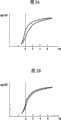
图3A是示出了依据比较例的薄膜晶体管的迟滞特性的曲线图。FIG. 3A is a graph showing hysteresis characteristics of a thin film transistor according to a comparative example.
图3B是示出了依据本发明的一个示例的薄膜晶体管的迟滞特性的曲线图。FIG. 3B is a graph showing hysteresis characteristics of a thin film transistor according to an example of the present invention.
图4是示出了基于In-Ga-Zn-O的非晶氧化物膜的电子载流子浓度与成膜期间的氧气分压之间的关系的曲线图。4 is a graph showing the relationship between the electron carrier concentration of an In-Ga-Zn-O-based amorphous oxide film and the oxygen partial pressure during film formation.
图5是非晶氧化物膜的制造设备的示意图。Fig. 5 is a schematic diagram of a manufacturing apparatus of an amorphous oxide film.
图6是示出了电阻率与基于In-Ga-Zn-O的非晶氧化物膜中掺杂的氢的量之间的关系的曲线图。6 is a graph showing the relationship between the resistivity and the amount of hydrogen doped in the In-Ga-Zn-O-based amorphous oxide film.
图7是示出了通过SIMS测量的深度方向上氢浓度的分布的曲线图。FIG. 7 is a graph showing the distribution of hydrogen concentration in the depth direction measured by SIMS.
具体实施方式Detailed ways
在下文中,将参考附图对本发明的实施例进行详细描述。Hereinafter, embodiments of the present invention will be described in detail with reference to the accompanying drawings.
图1A和1B是各自示出依据本发明的薄膜晶体管、即薄膜场效应晶体管的一个实施例的剖面视图。图1A是示出了顶栅结构的剖面视图,其中,在半导体沟道层11上以那种次序形成栅绝缘膜12和栅电极15。图1B是示出了底栅结构的剖视图,其中,在栅电极15上以那种次序形成栅绝缘膜12和半导体沟道层11。根据沟道层与绝缘膜之间的界面和电极的位置关系,把图1A中示出的结构称为交错结构,并把图1B中示出的结构称为反向交错结构。1A and 1B are cross-sectional views each showing an embodiment of a thin film transistor, ie, a thin film field effect transistor, according to the present invention. 1A is a sectional view showing a top gate structure in which a
如图1A所示,在形成于基底10上的半导体沟道层11上,顺序地形成源电极13、漏电极14、栅绝缘膜12、栅电极15,以便形成具有顶栅结构(交错结构)的场效应晶体管。另外,如图1B所示,在形成于基底10上的栅电极15上,顺序地形成栅绝缘膜12、半导体沟道层11、源电极13、以及漏电极14,以便形成具有底栅结构(反向交错结构)的场效应晶体管。As shown in FIG. 1A, on the
在图1A和图1B中示出的场效应晶体管各自是具有栅电极15、源电极13、以及漏电极14的三端子器件。上述场效应晶体管是具有如下功能的有源器件,其中,通过向栅电极施加电压Vg来控制流经沟道层的电流Id,即在源电极和漏电极之间流动的电流Id。The field effect transistors shown in FIGS. 1A and 1B are each a three-terminal device having a
在本发明中,TFT结构不限于上述结构,并且也可以使用任何顶栅或底栅结构,即任何交错或反向交错结构。In the present invention, the TFT structure is not limited to the above structure, and any top gate or bottom gate structure, ie any staggered or reverse staggered structure, can also be used.
图2A和2B示出了本发明的场效应晶体管(TFT)的典型特性。从具有要在示例1中描述的结构、并通过其中描述的制造方法形成的场效应晶体管中获得TFT的特性。当在源电极和漏电极之间施加大约5V的电压Vd时,并且当栅电压Vg在0到5V之间导通及关断时,可以(在导通和关断之间)控制在源电极和漏电极之间流动的电流Id。图2A示出了不同Vg值下的Id-Vd特性,并且图2B示出了6V的电压Vd下的Id-Vg特性(转移特性)。2A and 2B show typical characteristics of a field effect transistor (TFT) of the present invention. TFT characteristics were obtained from a field effect transistor having the structure to be described in Example 1 and formed by the manufacturing method described therein. When a voltage Vd of about 5V is applied between the source electrode and the drain electrode, and when the gate voltage Vg is turned on and off between 0 and 5V, the source electrode can be controlled (between on and off). and the current Id flowing between the drain electrode. FIG. 2A shows Id-Vd characteristics at different Vg values, and FIG. 2B shows Id-Vg characteristics (transfer characteristics) at a voltage Vd of 6V.
此实施例的TFT的沟道层由包含氢或氘的非晶氧化物膜形成。The channel layer of the TFT of this embodiment is formed of an amorphous oxide film containing hydrogen or deuterium.
参考图3A和3B,将描述通过向沟道层添加氢获得的效果,也就是迟滞现象的减少。图3A和3B分别示出了在比较例1和示例1中获得的TFT晶体管特性。也就是说,在示例1中,向沟道层添加氢,并且在比较例1中,不向沟道层添加氢。Referring to FIGS. 3A and 3B , the effect obtained by adding hydrogen to the channel layer, that is, reduction of hysteresis will be described. 3A and 3B show the TFT transistor characteristics obtained in Comparative Example 1 and Example 1, respectively. That is, in Example 1, hydrogen was added to the channel layer, and in Comparative Example 1, hydrogen was not added to the channel layer.
迟滞现象意味着,例如,为了评估TFT转移特性,在固定Vd的同时(向上和向下)扫描Vg时,通过如图3A所示的向上扫描和向下扫描,Id的值是不同的。当在预定的Vg下,Id值在向上扫描和向下扫描之间变化很大时,迟滞现象很大;因而,为了精确控制Id,具有小迟滞现象的器件是优选的。The hysteresis phenomenon means, for example, that when Vg is swept (up and down) while Vd is fixed in order to evaluate TFT transfer characteristics, the value of Id is different by scanning up and down as shown in FIG. 3A . When the value of Id varies greatly between scan-up and scan-down at a predetermined Vg, the hysteresis is large; thus, for precise control of Id, a device with small hysteresis is preferred.
当不包含氢时,迟滞现象特性如图3A所示,并且在使用了依据本发明的包含氢的沟道层时,可以获得如图3B所示的具有小迟滞现象的器件。When hydrogen is not contained, the hysteresis characteristics are as shown in FIG. 3A, and when the channel layer containing hydrogen according to the present invention is used, a device with small hysteresis as shown in FIG. 3B can be obtained.
从物理的观点来看,还不能清楚地理解在向沟道层施加包含氢的氧化物时迟滞现象减少的原因。一种估计的原因是通过添加氢来减轻非晶薄膜中的局部结构无序,并且结果是,实现了载流子不容易被俘获的非晶结构(深陷阱的数量减少)。另外,还可以解释为通过向沟道层添加氢减少了沟道层和绝缘膜之间的界面上的结构无序,并且结果是,在沟道层和绝缘膜之间实现了载流子不容易被俘获的界面。From a physical point of view, the reason for the reduction in hysteresis when an oxide containing hydrogen is applied to the channel layer has not been clearly understood. One estimated reason is to alleviate local structural disorder in the amorphous thin film by adding hydrogen, and as a result, an amorphous structure in which carriers are not easily trapped (the number of deep traps is reduced) is realized. In addition, it can also be explained that the structural disorder at the interface between the channel layer and the insulating film is reduced by adding hydrogen to the channel layer, and as a result, carrier separation is realized between the channel layer and the insulating film. An interface that is easy to capture.
为了评估迟滞现象,通过在把源-漏电压Vd固定在5到30V之间的适当值上的同时,在-10到30v的范围内(向上或向下)扫描栅电压Vg来测量Id(源漏电流)。在此测量中,将晶体管特性处于饱和区中的电压作为Vd,并且在导通和关断状态之间扫描Vg。然而,因为可以依赖于晶体管特性和晶体管结构来确定Vg和Vd的值,所以不总是把Vg和Vd限制为上述范围内。To evaluate hysteresis, Id(source leakage current). In this measurement, the voltage at which the transistor characteristics are in the saturation region is taken as Vd, and Vg is swept between on and off states. However, since the values of Vg and Vd can be determined depending on transistor characteristics and transistor structure, Vg and Vd are not always limited to the above-mentioned ranges.
可以通过向上扫描的Id-Vg曲线和向下扫描的Id-Vg曲线之间的差来评估迟滞现象的大小。例如,可以把从向上扫描的Id-Vg曲线和向下扫描的Id-Vg曲线获得的环的面积用于这种评估。当该面积很小时,可以说迟滞现象很小。另外,可以使用差值ΔVt=|Vtu-Vtd|来评估迟滞现象的大小,其中,Vtu是从向上扫描的Id-Vg曲线中估算的阈值电压,而Vtd是从向下扫描的Id-Vg曲线中估算的阈值电压。在下文中,这个ΔVt被称为阈值偏移量。小的ΔVt表示小的迟滞现象。The magnitude of the hysteresis can be evaluated by the difference between the upward-sweeping Id-Vg curve and the downward-sweeping Id-Vg curve. For example, the area of the ring obtained from the up-sweep Id-Vg curve and the down-sweep Id-Vg curve can be used for this evaluation. When the area is small, it can be said that hysteresis is small. Alternatively, the magnitude of hysteresis can be assessed using the difference ΔVt=|Vtu-Vtd|, where Vtu is the threshold voltage estimated from the upward-sweeping Id-Vg curve and Vtd is the threshold voltage from the downward-sweeping Id-Vg curve The estimated threshold voltage in . Hereinafter, this ΔVt is referred to as a threshold shift amount. A small ΔVt indicates a small hysteresis.
借助于依据本发明的使用包含氢的氧化物用于其沟道层的薄膜晶体管,可以实现具有小ΔVt的薄膜晶体管。With the thin film transistor using an oxide containing hydrogen for its channel layer according to the present invention, a thin film transistor having a small ΔVt can be realized.
因为本发明的薄膜晶体管的阈值偏移量取决于器件结构、沟道材料、评估条件、等等,因此例如在预定的条件下,优选地把施加到器件上的电压设为恒定值。作为本发明的薄膜晶体管的一个评估示例,可以使用阈值偏移量来执行评估,这种阈值偏移量是在10V的恒定Vg下,以100mV/秒的扫描速度在-5到15V的范围内(向上和向下)扫描Vg的情况中获得的。具体地,在上述的评估条件下,阈值偏移量可以减小到2V或更低,优选地为1V或更低,并且更优选地是0.5V或更低。Since the threshold shift amount of the thin film transistor of the present invention depends on the device structure, channel material, evaluation conditions, etc., it is preferable to set the voltage applied to the device to a constant value under predetermined conditions, for example. As an evaluation example of the thin film transistor of the present invention, evaluation can be performed using a threshold shift amount in the range of -5 to 15 V at a constant Vg of 10 V at a scan rate of 100 mV/sec (up and down) obtained in the case of scanning Vg. Specifically, under the evaluation conditions described above, the threshold shift amount can be reduced to 2 V or lower, preferably 1 V or lower, and more preferably 0.5 V or lower.
所需的迟滞现象的程度取决于薄膜晶体管的应用、要使用的电路结构等等。例如,对于液晶显示和电泳显示应用来说,要求相对较低;然而,对于有机EL显示器件、算术电路等等来说,需要更高的程度(更小的迟滞现象)。例如,对于有机EL显示器件应用来说,阈值偏移量优选地为2V或更低,更优选地为1V或更低。此外,对于更高性能的有机EL显示器件来说,阈值偏移量优选地为0.5V或更低。The degree of hysteresis required depends on the application of the thin film transistor, the circuit structure to be used, and the like. For example, for liquid crystal display and electrophoretic display applications, the requirements are relatively low; however, for organic EL display devices, arithmetic circuits, etc., a higher degree (less hysteresis) is required. For example, for an organic EL display device application, the threshold shift amount is preferably 2 V or less, more preferably 1 V or less. Furthermore, for a higher performance organic EL display device, the threshold shift amount is preferably 0.5 V or less.
(氢浓度和电子载流子浓度)(hydrogen concentration and electron carrier concentration)
另外,研究了具有由非晶氧化物构成的沟道层的薄膜晶体管。为了获得优异的TFT特性,有利地,使用具有0.0001到0.1S/cm范围内的电导率的半绝缘非晶氧化物膜作为沟道层。为了获得如上所述的电导率,尽管依赖于沟道层的材料组分,但是优选地形成具有大约1014到1018/cm3的电子载流子浓度的非晶氧化物膜。In addition, thin film transistors having a channel layer made of amorphous oxide have been studied. In order to obtain excellent TFT characteristics, it is advantageous to use a semi-insulating amorphous oxide film having a conductivity in the range of 0.0001 to 0.1 S/cm as the channel layer. In order to obtain the electrical conductivity as described above, although depending on the material composition of the channel layer, it is preferable to form an amorphous oxide film having an electron carrier concentration of about 1014 to 1018 /cm3 .
当电导率大于0.1S/cm时,就变得难以形成常断的晶体管,并且难以形成具有大的导通/关断比率的晶体管。在极端的情况下,即使在施加了栅电压时,也不能控制源电极和漏电极之间的电流的流动和停止,并且因而不能获得晶体管操作(开关)。When the conductivity is greater than 0.1 S/cm, it becomes difficult to form a normally-off transistor, and it becomes difficult to form a transistor with a large on/off ratio. In extreme cases, even when a gate voltage is applied, the flow and cessation of current between the source electrode and the drain electrode cannot be controlled, and thus transistor operation (switching) cannot be obtained.
另一方面,在使用了绝缘材料时,也就是说,在电导率小于0.0001S/cm时,就变得难以增大导通电流。在极端的情况下,即使在施加了栅电压时,也不能控制源电极和漏电极之间的电流的流动和停止,并且因而不能获得晶体管操作。On the other hand, when an insulating material is used, that is, when the electrical conductivity is less than 0.0001 S/cm, it becomes difficult to increase the conduction current. In extreme cases, even when a gate voltage is applied, the flow and cessation of current between the source electrode and the drain electrode cannot be controlled, and thus transistor operation cannot be obtained.
为了控制氧化物的电导率和电子载流子浓度,在成膜期间控制了氧分压。也就是说,通过控制氧分压,主要控制薄膜中的缺氧量,从而控制电子载流子浓度。图4是示出了在用溅射法形成基于In-Ga-Zn-O的氧化物薄膜时获得的载流子浓度对氧分压的依赖性的一个示例的曲线图。在实际上以高精度控制氧分压时,获得了具有1014到1018/cm3的载流子浓度的半绝缘非晶氧化物膜,并且在把这样获得的薄膜应用到沟道层时,可以形成良好的TFT。如图4所示,当典型地在大约0.005Pa的氧分压执行成膜时,可以获得半绝缘薄膜。当分压大于0.01Pa时,形成绝缘膜,而另一方面,当分压小于0.001Pa时,形成具有过高的电导率的膜;因而,优选地不把这样形成的膜应用到沟道层。然而,如图4所示,因为载流子浓度随氧分压中的变化而很灵敏地变化,所以特性受到成膜条件中微小变化的显著影响,结果,趋于难以获得TFT特性的可再现性。In order to control the conductivity and electron carrier concentration of the oxide, the oxygen partial pressure was controlled during film formation. That is, by controlling the oxygen partial pressure, the amount of oxygen deficiency in the film is mainly controlled, thereby controlling the electron carrier concentration. 4 is a graph showing one example of the dependence of carrier concentration on oxygen partial pressure obtained when an In-Ga-Zn-O-based oxide thin film is formed by a sputtering method. When oxygen partial pressure is actually controlled with high precision, a semi-insulating amorphous oxide film having a carrier concentration of 1014 to 1018 /cm3 is obtained, and when the film thus obtained is applied to a channel layer , can form a good TFT. As shown in FIG. 4 , when film formation is typically performed at an oxygen partial pressure of about 0.005 Pa, a semi-insulating thin film can be obtained. When the partial pressure is greater than 0.01Pa, an insulating film is formed, while on the other hand, when the partial pressure is less than 0.001Pa, a film having too high electrical conductivity is formed; thus, it is preferable not to apply the film thus formed to the channel layer. However, as shown in Fig. 4, since the carrier concentration changes very sensitively with changes in the oxygen partial pressure, the characteristics are greatly affected by slight changes in the film-forming conditions, and as a result, it tends to be difficult to obtain reproducible TFT characteristics sex.
依据本发明,通过添加氢(或氘)来控制电子载流子浓度。通过本发明的发明人所进行的深入的研究,发现了可以通过向非晶氧化物膜添加氢来控制电子载流子的量。According to the present invention, the electron carrier concentration is controlled by adding hydrogen (or deuterium). Through intensive studies conducted by the inventors of the present invention, it was found that the amount of electron carriers can be controlled by adding hydrogen to the amorphous oxide film.
例如,为了实现大约1018/cm3的电子载流子浓度,尽管依赖于成膜期间的氧分压和材料组分,但也可以添加氢以便具有大约1018到1020/cm3的浓度。在这种情况下,可以通过控制氢掺杂物的量来执行对电子载流子浓度的控制。另外,还可以通过氢掺杂物的量和缺氧的量来控制电子载流子浓度。For example, in order to realize an electron carrier concentration of about 1018 /cm3 , hydrogen may be added so as to have a concentration of about 1018 to 1020 /cm3 although depending on the oxygen partial pressure and material composition during film formation . In this case, control of the electron carrier concentration can be performed by controlling the amount of the hydrogen dopant. In addition, the electron carrier concentration can also be controlled by the amount of hydrogen dopants and the amount of oxygen deficiency.
因此,为了形成具有优秀特性的TFT,添加的氢的浓度优选地被控制在1016到1020/cm3的范围内。尽管依赖于氧分压和材料组分,但通过上述的氢的添加,可以实现具有大约1014到1018/cm3的电子载流子浓度且适于用作TFT的沟道层的氧化物薄膜。Therefore, in order to form a TFT having excellent characteristics, the concentration of added hydrogen is preferably controlled within a range of 1016 to 1020 /cm3 . Although depending on the oxygen partial pressure and material composition, by the above-mentioned addition of hydrogen, an oxide having an electron carrier concentration of about 1014 to 1018 /cm3 and suitable for use as a channel layer of a TFT can be realized film.
具体地,当把氢浓度设为1019/cm3或更小时,可以实现晶体管的常断操作和大的导通/关断比率。此外,氢浓度优选地被设为1017/cm3或更高,并且通过1017/cm3或更高的氢浓度,可以更有效地减少晶体管的迟滞现象。Specifically, when the hydrogen concentration is set to 1019 /cm3 or less, normally-off operation of the transistor and a large on/off ratio can be realized. In addition, the hydrogen concentration is preferably set to 1017 /cm3 or higher, and by the hydrogen concentration of 1017 /cm3 or higher, hysteresis of the transistor can be reduced more effectively.
例如,可以通过二次离子质谱法(SIMS)来评估氢浓度。尽管依赖于评估设备,检测极限大约为1017/cm3。在小于检测极限的区域内,可以通过以薄膜中的氢浓度和用于添加氢的工艺参数(氢分压或者稍后将描述的成膜期间的离子注入量)之间存在线性关系的假定为基础的外插法来间接获得氢浓度。For example, hydrogen concentration can be estimated by secondary ion mass spectrometry (SIMS). Although dependent on the evaluation equipment, the detection limit is about 1017 /cm3 . In the region smaller than the detection limit, it can be assumed that there is a linear relationship between the hydrogen concentration in the thin film and the process parameter for adding hydrogen (hydrogen partial pressure or ion implantation amount during film formation to be described later) as Basic extrapolation to obtain hydrogen concentrations indirectly.
用下列等式(不包括氢)来表示本发明中由包含了氢的非晶氧化物构成的沟道层的组成成分:The composition of the channel layer made of amorphous oxide containing hydrogen in the present invention is represented by the following equation (excluding hydrogen):
[(Sn1-xM4x)O2]a·[(In1-yM3y)2O3]b·[(Zn1-zM2zO)]c[(Sn1-x M4x )O2 ]a·[(In1-y M3y )2 O3 ]b·[(Zn1-z M2z O)]c
其中,满足0≤x≤1,0≤y≤1,0≤z≤1,0≤a<1,0≤b<1,0≤c<1,以及a+b+c=1,Among them, satisfying 0≤x≤1, 0≤y≤1, 0≤z≤1, 0≤a<1, 0≤b<1, 0≤c<1, and a+b+c=1,
M4是具有比Sn小的原子序数的第IV族的元素(Si、Ge、或Zr),M4 is an element of Group IV (Si, Ge, or Zr) having an atomic number smaller than Sn,
M3是Lu或者具有比In小的原子序数的第III族的元素(B、Al、Ga、或Y),以及M3 is Lu or an element of Group III having an atomic number smaller than In (B, Al, Ga, or Y), and
M2是具有比Zn小的原子序数的第II族的元素(Mg或Ca)。M2 is a Group II element (Mg or Ca) having an atomic number smaller than Zn.
在上述的组成成分中,具体地,下列组合是优选的,即,[(In1-yGay)2O3]b·[(ZnO)]c,其中,满足0≤y≤1,0<b<1,以及0<c<1,以及[(SnO2)]a·[(In2O3)]b·[(ZnO)]c,其中,满足0≤a≤1,0<b<1,以及0<c<1。Among the above-mentioned constituents, specifically, the following combination is preferable, namely, [(In1-y Gay )2 O3 ]b·[(ZnO)]c, wherein 0≤y≤1, 0 <b<1, and 0<c<1, and [(SnO2 )]a·[(In2 O3 )]b·[(ZnO)]c, where 0≤a≤1, 0<b <1, and 0<c<1.
例如,可以用下列组分来实现依据本发明的包含氢的非晶氧化物膜。也就是说,非晶氧化物膜具有位于拥有3个峰Ga2O3、In2O3、以及ZnO的三角形内的二重组分或三重组分,或者具有位于拥有3个峰SnO2、In2O3、以及ZnO的三角形内的二重组分或三重组分。在某些情况下,可以使特定组分范围内的某些三重组分结晶。特别地,一重组分并非优选,这是因为其被结晶。例如,在包含了上述3种化合物中的两种的二重组分(位于上述三角形一边上的组分)中,包含有20到70原子百分比的In的基于In-Zn-O的组分可以形成非晶膜。另外,对于基于Sn-In-O的组分,可以由包含20到80原子百分比的In的组分形成非晶膜。For example, the hydrogen-containing amorphous oxide film according to the present invention can be realized with the following components. That is, the amorphous oxide film has a double or triple composition located within a triangle having three peaks of Ga2 O3 , In2 O3 , and ZnO, or has a double or triple composition located within a triangle having three peaks of SnO2 , In 22 O3 , and a triangular double or triple composition of ZnO. In some cases, certain triplets within specific compositional ranges can be crystallized. In particular, one component is not preferred because it is crystallized. For example, in a dual composition (a composition located on one side of the above triangle) containing two of the above three compounds, an In-Zn-O-based composition containing 20 to 70 atomic percent of In can form Amorphous film. In addition, as for the Sn-In-O-based composition, an amorphous film can be formed from a composition containing 20 to 80 atomic percent of In.
当如本发明所描述的那样把氢原子添加到非晶氧化物膜中时,可以在室温下进一步稳定该非晶膜。因此,可以在很宽的三重组分范围内形成非晶氧化物。When hydrogen atoms are added to the amorphous oxide film as described in the present invention, the amorphous film can be further stabilized at room temperature. Thus, amorphous oxides can be formed over a wide range of ternary compositions.
(制造方法)(Manufacturing method)
作为一种用于形成依据本发明的包含氢的特定非晶氧化物的方法,例如,可以提及:As a method for forming the specific amorphous oxide containing hydrogen according to the present invention, for example, can be mentioned:
(1)用于在成膜期间在预定的分压下在成膜设备中提供包含氢原子的气体(除水蒸气之外)的同时形成膜的方法;(1) A method for forming a film while supplying a gas (other than water vapor) containing hydrogen atoms in a film forming apparatus at a predetermined partial pressure during film formation;
(2)用于使用包含氢的材料源形成膜的方法;以及(2) a method for forming a film using a material source comprising hydrogen; and
(3)用于形成膜,然后通过离子注入或氢等离子加工而向其内部添加氢的方法。(3) A method for forming a film and then adding hydrogen to the inside thereof by ion implantation or hydrogen plasma processing.
在上面的那些方法中,考虑到氢浓度的可控性,使用离子注入的方法(3)是优选的。然而,因为离子注入是在成膜之后执行的,所以不利地增加了步骤的数目,并且在膜厚度方向上还不利地产生了氢浓度的分布。另一方面,作为成膜工艺,方法(2)很简单;然而,不能容易地准备包含氢的材料源,并且不能容易地控制膜中的氢浓度。借助于用成膜气体环境中的氢分压来控制膜中的氢浓度的方法(1),可控性优秀,另外,制造工艺也相对比较简单。因此,最优选使用在包含氢的气体中形成膜的方法(1)。Among those methods above, the method (3) using ion implantation is preferable in view of the controllability of the hydrogen concentration. However, since ion implantation is performed after film formation, the number of steps disadvantageously increases, and also disadvantageously produces a distribution of hydrogen concentration in the film thickness direction. On the other hand, method (2) is simple as a film-forming process; however, a material source containing hydrogen cannot be easily prepared, and the hydrogen concentration in the film cannot be easily controlled. The method (1) of controlling the hydrogen concentration in the film by using the hydrogen partial pressure in the film-forming gas environment has excellent controllability, and in addition, the manufacturing process is relatively simple. Therefore, the method (1) of forming a film in a hydrogen-containing gas is most preferably used.
作为在方法(1)使用的包含氢的气体,例如可以提及氢气、氘气、以及烃气体。考虑到气体分压的可控性和气体的安全性,尤其优选地使用以氩气稀释的氢气。As the hydrogen-containing gas used in the method (1), for example, hydrogen gas, deuterium gas, and hydrocarbon gas can be mentioned. In consideration of the controllability of the partial pressure of the gas and the safety of the gas, it is especially preferable to use hydrogen diluted with argon.
另外,作为在离子注入法(3)中使用的离子物类,例如可以提及H+离子、H-离子、D+离子(氘离子)、以及H2+离子(氢分子离子)。In addition, as ion species used in the ion implantation method (3), for example, H+ ions, H− ions, D+ ions (deuterium ions), and H2+ ions (hydrogen molecular ions) can be mentioned.
作为用于形成非晶氧化物膜的方法,优选地使用诸如溅射法(SP方法)、脉冲激光沉积法(PLD法)、或者电子束沉积法之类的汽相法。在上述的汽相法中,考虑到大规模生产能力,适合使用SP法。然而,成膜法不限于上述的那些方法。对于基底的温度而言,不一定有意地执行加热,因此基底可以保持在大约室温上。As a method for forming the amorphous oxide film, a vapor phase method such as a sputtering method (SP method), a pulsed laser deposition method (PLD method), or an electron beam deposition method is preferably used. Among the vapor phase methods described above, the SP method is suitably used in consideration of large-scale productivity. However, the film-forming methods are not limited to those described above. With respect to the temperature of the substrate, heating does not necessarily have to be performed intentionally, so the substrate can be kept at about room temperature.
已知在氢气气体环境中对具有低电子载流子浓度的非晶氧化物膜进行热处理时,缺氧增加,因而,电子载流子浓度可以增大;然而,高温热处理是不利的。另外,难以精确地控制载流子浓度。It is known that when an amorphous oxide film having a low electron carrier concentration is heat-treated in a hydrogen gas atmosphere, oxygen deficiency increases and thus, the electron carrier concentration can increase; however, high-temperature heat treatment is disadvantageous. In addition, it is difficult to precisely control the carrier concentration.
如上所述,例如,通过在包含氢的气体中执行的成膜或者通过在成膜之后执行的离子注入,用非晶氧化物膜中的氢浓度来控制电子载流子浓度。因此,能够可再现地获得具有1014到1018/cm3的电子载流子浓度的半绝缘非晶氧化物膜。当如上所述的包含氢的非晶氧化物被应用到薄膜晶体管的沟道层时,能够可再现地形成具有小迟滞现象的晶体管。As described above, the electron carrier concentration is controlled with the hydrogen concentration in the amorphous oxide film, for example, by film formation performed in a hydrogen-containing gas or by ion implantation performed after film formation. Therefore, a semi-insulating amorphous oxide film having an electron carrier concentration of 1014 to 1018 /cm3 can be reproducibly obtained. When the amorphous oxide containing hydrogen as described above is applied to a channel layer of a thin film transistor, a transistor having a small hysteresis can be reproducibly formed.
在依据本发明的晶体管中,作为用于栅绝缘膜12的材料,可以使用任何材料,只要其具有优秀的绝缘特性。例如,作为栅绝缘膜12,可以使用Al2O3、Y2O3、HfO2、或者包含了至少两种上述化合物的混合化合物。结果,源电极和漏电极之间的泄漏电流与漏电极和栅电极之间的泄漏电流可以减小到大约10-7A。In the transistor according to the present invention, as a material for the
另外,作为用于源电极13、漏电极14、以及栅电极15的材料,可以使用任何材料,只要其具有良好的导电性并且可电连接到沟道层。例如,可以使用由In2O3:Sn、ZnO等制成的透明导电膜或者由Au、Pt、Al、Ni等制成的金属膜。In addition, as materials for
作为基底10,例如可以使用玻璃基底、塑料基底、或者塑料膜。As the
因为上述的沟道层和栅绝缘膜对于可见光是透明的,所以当把透明材料用作用于上述电极和基底的材料时,可以形成透明的薄膜晶体管。Since the above-mentioned channel layer and gate insulating film are transparent to visible light, when a transparent material is used as a material for the above-mentioned electrode and substrate, a transparent thin film transistor can be formed.
迄今为止,尽管已借助于示例描述了包含In-Ga-Zn的非晶氧化物,但是可以把包含Sn、In、以及Zn中至少一种的非晶氧化物应用到本发明的沟道层。So far, although an amorphous oxide containing In-Ga-Zn has been described by way of example, an amorphous oxide containing at least one of Sn, In, and Zn may be applied to the channel layer of the present invention.
此外,当选择Sn作为非晶氧化物的至少一种组成元素时,可以用Sn1-xM4x来代替Sn,(其中满足0<x<1,并且M4是具有比Sn小的原子序数的第IV族的元素(Si、Ge、或者Zr))。In addition, when Sn is selected as at least one constituent element of the amorphous oxide, Sn can be replaced by Sn1-x M4x , (where 0<x<1 is satisfied, and M4 has an atomic number smaller than Sn Group IV elements (Si, Ge, or Zr)).
另外,当选择In作为非晶氧化物的至少一种组成元素时,可以用In1-yM3y来代替In,(其中满足0<y<1,并且M3是Lu或者具有比In小的原子序数的第III族的元素(B、Al、Ga或者Y))。In addition, when In is selected as at least one constituent element of the amorphous oxide, In1-y M3y can be used instead of In, (where 0<y<1 is satisfied, and M3 is Lu or has atoms smaller than In ordinal group III element (B, Al, Ga or Y)).
另外,当选择Zn作为非晶氧化物的至少一种组成元素时,可以用Zn1-zM2z来代替Zn,(其中满足0<z<1,并且M2是具有比Zn小的原子序数的第II族的元素(Mg或者Ca))。In addition, when Zn is selected as at least one constituent element of the amorphous oxide, Zn may be replaced by Zn1-z M2z , (where 0<z<1 is satisfied, and M2 has an atomic number smaller than Zn Group II elements (Mg or Ca)).
作为适用于本发明的非晶氧化物,例如,可以提及Ga-In-Zn氧化物、Sn-In-Zn氧化物、In-Zn-Ga-Mg氧化物、In氧化物、In-Sn氧化物、In-Ga氧化物、In-Zn氧化物、以及Zn-Ga氧化物。当然,组成元素之间的组分比不总是需要为1∶1。另外,可能难以仅由Zn或Sn自身形成非晶相;然而,当包含In时,可以很容易地形成非晶相。例如,在基于In-Zn的系统的情况下,在金属元素中包含大约20-70原子百分比的In的组分的情况下,形成非晶膜。在基于Sn-In的系统的情况下,在金属元素中包含大约20-80原子百分比的In的组分的情况下,形成非晶膜。在基于Sn-In-Zn的系统的情况下,在金属元素中包含大约15原子百分比或更高的In的组分的情况下,形成非晶膜。As the amorphous oxide suitable for the present invention, for example, Ga-In-Zn oxide, Sn-In-Zn oxide, In-Zn-Ga-Mg oxide, In oxide, In-Sn oxide material, In-Ga oxide, In-Zn oxide, and Zn-Ga oxide. Of course, the composition ratio between constituent elements does not always need to be 1:1. In addition, it may be difficult to form an amorphous phase only from Zn or Sn itself; however, when In is contained, an amorphous phase can be easily formed. For example, in the case of an In—Zn-based system, an amorphous film is formed with a component containing about 20 to 70 atomic percent of In among metal elements. In the case of the Sn—In-based system, an amorphous film is formed with a component containing about 20 to 80 atomic percent of In in the metal element. In the case of the Sn-In-Zn-based system, with a component containing about 15 atomic percent or more of In in the metal element, an amorphous film is formed.
另外,当以大约0.5°的小入射角对薄膜执行x射线衍射测量时,因为检测不到清楚的衍射峰值(也就是说,观测到空心图案(hollowpattern)),所以可以确认非晶相。在本发明中,当把上述的材料用于场效应晶体管的沟道层时,该沟道层还可以包含微细结晶。In addition, when x-ray diffraction measurement was performed on the thin film at a small incident angle of about 0.5°, an amorphous phase could be confirmed because no clear diffraction peak was detected (that is, a hollow pattern was observed). In the present invention, when the above-mentioned materials are used for the channel layer of the field effect transistor, the channel layer may also contain fine crystals.
另外,本发明的另一实施例涉及用于制造用于场效应晶体管的沟道层的非晶氧化物膜的方法;这种方法包括下述的第一和第二步骤。In addition, another embodiment of the present invention relates to a method for manufacturing an amorphous oxide film for a channel layer of a field effect transistor; this method includes first and second steps described below.
第一步骤是在成膜设备中布置基底的步骤。The first step is a step of arranging a substrate in a film forming apparatus.
第二步骤是在以各自预定的分压在成膜设备中提供包含氢原子的气体(除水蒸气之外)和氧气的同时在基底上形成非晶氧化物膜的步骤。The second step is a step of forming an amorphous oxide film on the substrate while supplying a gas containing hydrogen atoms (other than water vapor) and oxygen at respective predetermined partial pressures in the film forming apparatus.
如之前参考图4描述的那样,当想要仅通过氧分压来控制电导率和载流子浓度时,必须在窄区域中控制电导率,在这个区域中电导率取决于氧分压而急剧变化。As previously described with reference to Fig. 4, when one wants to control the conductivity and carrier concentration only by the oxygen partial pressure, the conductivity must be controlled in a narrow region where the conductivity depends on the oxygen partial pressure sharply. Variety.
当如在本发明的情况下那样使用了包含氢原子的气体诸如氢气时,例如,氧分压被设为0.008Pa或更高,并且优选地被设为0.01Pa或更高。可以通过调节包含氢原子的气体的分压来控制非晶氧化物膜的电导率。When a gas containing hydrogen atoms such as hydrogen gas is used as in the case of the present invention, for example, the oxygen partial pressure is set to 0.008 Pa or higher, and is preferably set to 0.01 Pa or higher. The electrical conductivity of the amorphous oxide film can be controlled by adjusting the partial pressure of the gas containing hydrogen atoms.
在借助于示例的上述范围内,例如与大约0.005Pa的氧分压的区域相比,载流子浓度对氧分压的依赖性不是那么高。In the aforementioned range by way of example, the dependence of the carrier concentration on the oxygen partial pressure is not so high, for example, compared to the region of an oxygen partial pressure of approximately 0.005 Pa.
也可以用氢分压调节载流子浓度,另外,因为与对氧分压的依赖性相比,载流子浓度对氢分压的依赖性很低,结果,可以提高成膜气体环境的可控性。The carrier concentration can also be adjusted by the hydrogen partial pressure. In addition, since the carrier concentration has a low dependence on the hydrogen partial pressure compared with the dependence on the oxygen partial pressure, as a result, the reliability of the film-forming gas environment can be improved. controlling.
氧分压的上限例如是0.1Pa。这个上限可选地可被设置在0.05到0.5Pa的范围内。The upper limit of the oxygen partial pressure is, for example, 0.1 Pa. This upper limit can optionally be set in the range of 0.05 to 0.5 Pa.
尽管优选的氢分压也依赖于氧分压,但是,其在例如0.001到0.01Pa的范围内。Although the preferred hydrogen partial pressure also depends on the oxygen partial pressure, it is in the range of, for example, 0.001 to 0.01 Pa.
另外,优选不使用水蒸气,这是因为对氧和氢的分压的控制在某些情况下可能变得困难。In addition, it is preferable not to use water vapor, since control of the partial pressures of oxygen and hydrogen may become difficult in some cases.
并不总是需要在成膜步骤期间把氢包含在氧化物膜中。可以通过在成膜之后执行的步骤中添加氢而把氢包含在氧化物膜中。It is not always necessary to contain hydrogen in the oxide film during the film forming step. Hydrogen can be contained in the oxide film by adding hydrogen in a step performed after film formation.
作为具体的氢添加方法,例如可以提及包含氢的离子注入或者等离子处理。As a specific hydrogen addition method, for example, ion implantation or plasma treatment containing hydrogen can be mentioned.
示例1Example 1
在这个示例中,形成了图1A中示出的顶栅TFT。在这个示例中,沟道层是在包含氢的气体环境中通过溅射法形成的基于In-Ga-Zn-O的非晶氧化物。In this example, the top-gate TFT shown in FIG. 1A was formed. In this example, the channel layer is an In-Ga-Zn-O-based amorphous oxide formed by a sputtering method in a hydrogen-containing gas atmosphere.
首先,在玻璃基底上(Corning公司生产的Corning #1737玻璃)形成包含氢的非晶氧化物膜作为沟道层。First, an amorphous oxide film containing hydrogen was formed as a channel layer on a glass substrate (Corning #1737 glass produced by Corning Corporation).
在这个示例中,在包含氩气、氧气、以及氢气的混合气体气体环境中通过高频的溅射形成包含氢的基于In-Ga-Zn-O的非晶氧化物膜。In this example, an In-Ga-Zn-O-based amorphous oxide film containing hydrogen was formed by high-frequency sputtering in a mixed gas atmosphere containing argon, oxygen, and hydrogen.
使用如图5所示的溅射设备。在这幅图中,附图标记51表示试样,附图标记52表示靶,附图标记53表示真空泵,附图标记54表示真空计,附图标记55表示基底保持件,附图标记56表示为每一气体引入系统提供的气体流速控制器,附图标记57表示压力控制器,并且附图标记58表示成膜室。Use the sputtering apparatus shown in Figure 5. In this drawing,
真空泵53用来对成膜室58的内部进行抽真空。基底保持件55用来把基底保持在成膜室58内部;氧化物膜形成在基底上。把材料源(靶)52布置为面向基底保持件55。此外,在溅射的成膜设备中,提供有使材料源的材料蒸发的能量源(高频电源,未示出)、用于向成膜室58中提供氢气的装置、以及用于向成膜室58中提供氧气的装置。The
作为气体引入系统,提供有用于氩气、氩气和氧气的混合气体(Ar∶O2=80∶20)、以及氩气和氢气的混合气体(Ar∶H2=98∶2)的3条线路。通过独立控制各个气体流速的气体流速控制器56以及控制泵速的压力控制器57,可以在成膜室58中获得预定的气体环境。As a gas introduction system, three lines for argon, argon and oxygen mixed gas (Ar:O2 =80:20), and argon and hydrogen mixed gas (Ar:H2 =98:2) are provided line. A predetermined gas environment can be obtained in the
在这个示例中,尽管使用了氩气和氧气的混合气体以及氩气与氢气的混合气体,但是也可以使用纯氢气和纯氧气。另外,在这个示例中,通过用于氩气、氩气和氧气的混合气体、氩气与氢气的混合气体的3条线路来执行气体引入;然而,可以通过用于氩气、氧气和氢气的混合气体的一条线路或者通过用于氩气与氧气的混合气体以及氩气与氢气的混合气体的2条线路来执行气体引入。In this example, although a mixed gas of argon and oxygen and a mixed gas of argon and hydrogen were used, pure hydrogen and pure oxygen may also be used. Also, in this example, gas introduction is performed by 3 lines for argon, argon-oxygen mixed gas, and argon-hydrogen mixed gas; Gas introduction is performed by one line of the mixed gas or by 2 lines for the mixed gas of argon and oxygen and the mixed gas of argon and hydrogen.
在这个示例中,作为靶(材料源),使用了InGaO3(ZnO)的2英寸的多晶烧结材料,并且输入RF功率被设为100W。在成膜气体环境中,总压力被设为0.4Pa,并且作为气体流速比率,满足Ar∶O2∶H2=100∶4∶1。沉积速率为12nm/分钟。此外,基底温度不被加热并且保持在大约25℃的室温下。In this example, as a target (material source), a 2-inch polycrystalline sintered material of InGaO3 (ZnO) was used, and the input RF power was set to 100W. In the film-forming gas atmosphere, the total pressure was set to 0.4 Pa, and as the gas flow rate ratio, Ar:O 2 :H2 =100:4:1 was satisfied. The deposition rate was 12 nm/min. In addition, the substrate temperature was not heated and kept at room temperature of about 25°C.
当通过掠入射x射线衍射(薄膜方法,0.5°的入射角)来评估这样形成的膜时,没有观测到清楚的衍射峰值,因而可以理解,这样形成的基于In-Zn-Ga-O的膜是非晶膜。When the film thus formed was evaluated by grazing incidence x-ray diffraction (thin film method, incident angle of 0.5°), no clear diffraction peak was observed, so it can be understood that the In-Zn-Ga-O-based film thus formed is an amorphous film.
此外,椭圆偏振光谱法测量和分析示出,该薄膜的均方粗糙度(Rrms)大约为0.5nm,并且膜厚度大约为60nm。依据荧光x射线(XRF)分析的结果,薄膜中的金属组分比为In∶Ga∶Zn=39∶37∶24。In addition, spectroscopic ellipsometry measurement and analysis showed that the mean square roughness (Rrms) of the thin film was about 0.5 nm, and the film thickness was about 60 nm. According to the results of fluorescence x-ray (XRF) analysis, the metal composition ratio in the thin film is In:Ga:Zn=39:37:24.
另外,通过使用SIMS进行组分分析,估算薄膜中的氢浓度为4×10¹⁸(l/cm3)。In addition, by component analysis using SIMS, the hydrogen concentration in the thin film was estimated to be 4×10¹⁸ (l/cm3 ).
另外,电导率大约为10-1S/cm,并且电子载流子浓度和电子迁移率分别被估算为大约4×1016/cm3和2cm2/V·秒。另外,根据光吸收光谱测定分析,估算出这样形成的非晶氧化物膜的能带间隙大约为3eV。In addition, the electrical conductivity was about 10-1 S/cm, and the electron carrier concentration and electron mobility were estimated to be about 4×10¹⁶ /cm3 and 2 cm2 /V·sec, respectively. In addition, the energy band gap of the amorphous oxide film thus formed was estimated to be about 3 eV from optical absorption spectrometry analysis.
接着,利用光刻法和剥离(lift-off)法,通过图案化来形成漏电极14和源电极13。各自的电极材料为Au,并且其厚度是30nm。Next,
接着,利用光刻法和剥离法,通过图案化来形成栅绝缘膜12。对于栅绝缘膜,通过电子束沉积法形成具有150nm厚度的Y2O3膜。另外,该Y2O3膜的相对介电常数大约为15。Next,
此外,通过光刻法和剥离法,形成栅电极15。沟道长度和沟道宽度分别是50μm和200μm。电极材料是Au,并且厚度为30nm。In addition,
比较例1Comparative example 1
在形成沟道层时,不提供氢,并且仅提供氩和氧,从而形成TFT。在成膜气体环境中,总压力为0.4Pa,并且在这种情况下,气体流速比Ar比O2被设为100比1,使得氧分压为0.004Pa。成膜速率为14nm/分钟。另外,基底温度不被加热并且保持在大约25℃的室温下。When forming the channel layer, hydrogen was not supplied, and only argon and oxygen were supplied, thereby forming a TFT. In the film-forming gas environment, the total pressure was 0.4 Pa, and in this case, the gas flow rate ratio Ar toO2 was set to 100 to 1, so that the oxygen partial pressure was 0.004 Pa. The film formation rate was 14 nm/min. In addition, the substrate temperature was not heated and kept at room temperature of about 25°C.
图4是示出了在如上所述的非晶氧化物薄膜的电导率的变化的曲线图,当氧分压变化时获得这种电导率的变化。如图所示,在用于TFT形成的氧分压的范围内,随着氧分压中的微小变化,电导率发生显著的变化;因而,必须精确地控制氧分压。FIG. 4 is a graph showing the change in electrical conductivity of the amorphous oxide thin film as described above, which is obtained when the oxygen partial pressure is changed. As shown, within the range of oxygen partial pressures used for TFT formation, electrical conductivity varies significantly with small changes in oxygen partial pressure; thus, the oxygen partial pressure must be precisely controlled.
(TFT的特性评估)(Evaluation of TFT characteristics)
图2A和2B是各自示出了在室温下测量的TFT的电流-电压特性的曲线图。图2A示出了Id-Vd特性,图2B示出了Id-Vg特性。如图2A所示,当在施加了恒定的栅电压Vg的同时测量源电极和漏电极之间的电流Id对漏电压Vd的依赖性时,示出了典型的半导体晶体管性状,其中,在大约6V的漏电压Vd上Id饱和(夹断)。在测量转移特性时,4V的漏电压Vd处的栅电压的阈值电压VG大约为-0.5V。另外,当栅电压Vg为10V时,流过大约1.0×10⁻⁵A的电流Id。2A and 2B are graphs each showing a current-voltage characteristic of a TFT measured at room temperature. FIG. 2A shows Id-Vd characteristics, and FIG. 2B shows Id-Vg characteristics. As shown in FIG. 2A, when the dependence of the current Id between the source electrode and the drain electrode on the drain voltage Vd is measured while a constant gate voltage Vg is applied, typical semiconductor transistor behavior is shown, wherein, at about Id saturates (pinches off) at a drain voltage Vd of 6V. When the transfer characteristics were measured, the threshold voltageVG of the gate voltage at the drain voltage Vd of 4V was about −0.5V. In addition, when the gate voltage Vg is 10V, a current Id of about 1.0×10⁻⁵ A flows.
晶体管的导通/关断比高于106。另外,在从输出特性中计算电子场效应迁移率时,在饱和区获得大约8cm2·(Vs)-1的场效应迁移率。用可见光照射这样形成的器件并且以类似于上述的方式测量这种器件;然而,根本没有观测到晶体管特性的变化。The on/off ratio of the transistor is higher than 106 . In addition, when the electron field-effect mobility is calculated from the output characteristics, a field-effect mobility of about 8 cm2 ·(Vs)-1 is obtained in the saturation region. The device thus formed was irradiated with visible light and measured in a manner similar to that described above; however, no change in transistor characteristics was observed at all.
另外,这个示例的TFT的迟滞现象小于比较例的TFT的迟滞现象。图3A和3B是分别示出了比较例和这个示例的Id-Vg关系的曲线图。Id-Vg关系是TFT特性中的一种。如图所示,通过向沟道层添加氢,可以减小TFT的迟滞现象。In addition, the hysteresis of the TFT of this example is smaller than that of the TFT of the comparative example. 3A and 3B are graphs showing the Id-Vg relationship of the comparative example and this example, respectively. The Id-Vg relationship is one of TFT characteristics. As shown in the figure, by adding hydrogen to the channel layer, the hysteresis of the TFT can be reduced.
另外,与比较例的情况相比,在这个示例中能够可再现地形成TFT,并且这样形成的器件的特性的变动趋向于减小。可以相信,因为与比较例相比,在这个示例中可以在高氧分压下执行成膜,所以能够可再现地形成TFT。另外,还可以相信,因为可以在包含氢的气体环境中形成沟道层,所以减小了TFT特性随氧分压的微小变化的变化,因而减小了特性的变动。In addition, TFTs can be reproducibly formed in this example as compared with the case of the comparative example, and variations in the characteristics of the devices thus formed tend to be reduced. It is believed that since film formation can be performed at a high oxygen partial pressure in this example compared with the comparative example, TFTs can be formed reproducibly. In addition, it is also believed that since the channel layer can be formed in a gas atmosphere containing hydrogen, variations in TFT characteristics with minute changes in oxygen partial pressure are reduced, thereby reducing variations in characteristics.
在比较例中氧分压实际上大约为5mPa,而在这个示例中大约为0.015Pa。如图4所示,在比较例中,在溅射法中不添加氢的情况下控制氧分压。然后,形成具有适于TFT沟道层的电子载流子浓度的薄膜。因而,必须把氧分压设为大约5mPa的压力。如上所述,因为在这种条件下,载流子浓度随氧分压的变化而灵敏地变化,所以特性受到成膜条件中的微小变化的显著影响,结果,趋于难以可再现地获得优秀的TFT特性。The oxygen partial pressure is actually about 5 mPa in the comparative example, and about 0.015 Pa in this example. As shown in FIG. 4 , in the comparative example, the oxygen partial pressure was controlled without adding hydrogen in the sputtering method. Then, a thin film having an electron carrier concentration suitable for the TFT channel layer is formed. Therefore, it is necessary to set the oxygen partial pressure to a pressure of about 5 mPa. As described above, since under such conditions, the carrier concentration changes sensitively with changes in the oxygen partial pressure, the characteristics are significantly affected by slight changes in the film-forming conditions, and as a result, it tends to be difficult to reproducibly obtain excellent TFT characteristics.
另一方面,在这个示例中,通过添加氢来控制电子载流子浓度。在这个示例中,除了添加氢之外,还把0.01Pa或更高的压力用作氧分压。如图4所示,不添加氢而在这个氧分压(>0.01Pa)下形成的膜是绝缘材料,因而,充分地减少了电子缺乏和电子载流子浓度。在这个示例中,以相对较高的氧分压在包含氢的气体环境中形成膜。通过上述的方法,特性不受到氧分压的微小变化的显著影响,因而可以获得期望的电子载流子浓度。因此,能够可再现地形成具有小的特性变动的晶体管。On the other hand, in this example, the electron carrier concentration is controlled by adding hydrogen. In this example, in addition to adding hydrogen, a pressure of 0.01 Pa or higher was used as the oxygen partial pressure. As shown in FIG. 4, a film formed at this oxygen partial pressure (>0.01 Pa) without adding hydrogen is an insulating material, and thus, electron deficiency and electron carrier concentration are sufficiently reduced. In this example, the film was formed in a hydrogen-containing gas environment at a relatively high oxygen partial pressure. By the method described above, the characteristics are not significantly affected by minute changes in the oxygen partial pressure, and thus a desired electron carrier concentration can be obtained. Therefore, it is possible to reproducibly form transistors with small fluctuations in characteristics.
另外,在测量包含氢的非晶氧化物膜的电子载流子浓度和电子迁移率时,在成膜气体环境中以不同的氢分压获得非晶氧化物膜,当氢分压增加时,载流子浓度和电子迁移率趋于增加。通过空穴迁移率测量来执行这种估计。In addition, when measuring the electron carrier concentration and electron mobility of the amorphous oxide film containing hydrogen, the amorphous oxide film was obtained at different hydrogen partial pressures in the film-forming gas environment, and when the hydrogen partial pressure increased, The carrier concentration and electron mobility tend to increase. This estimation is performed by hole mobility measurements.
在一般的化合物中,当载流子浓度增加时,由于在载流子等之间的分散引起电子迁移率减小;然而,在本发明的包含氢的非晶氧化物中,当电子载流子浓度增加时,电子迁移率也增加。还未很好地理解这种现象的物理机制。In a general compound, when the carrier concentration increases, electron mobility decreases due to dispersion among carriers etc.; however, in the amorphous oxide containing hydrogen of the present invention, when electrons carry As the subconcentration increases, the electron mobility also increases. The physical mechanism of this phenomenon is not well understood.
在向栅电极施加电压时,因为电子被注入在上述的非晶氧化物沟道层中,所以电流在源电极和漏电极之间流动,使得其间的区域进入导通状态。在本发明的非晶氧化物膜中,因为电子载流子浓度增加时电子迁移率增加,所以当晶体管处于导通状态时电流可以进一步增大。也就是说,饱和电流和导通/关断比可以进一步增大。When a voltage is applied to the gate electrode, since electrons are injected into the above-mentioned amorphous oxide channel layer, current flows between the source electrode and the drain electrode, bringing the region therebetween into a conduction state. In the amorphous oxide film of the present invention, since the electron mobility increases when the electron carrier concentration increases, the current can be further increased when the transistor is in an on state. That is, the saturation current and the on/off ratio can be further increased.
期望把本发明的具有相对较高的场效应迁移率的场效应晶体管应用到例如有机发光二极管的运算电路。It is desired to apply the field effect transistor having relatively high field effect mobility of the present invention to operational circuits such as organic light emitting diodes.
示例2Example 2
在这个示例中,将对包含氢的非晶氧化物膜进行描述,这种非晶氧化物膜要用于薄膜晶体管的沟道层。首先,在石英基底上形成非晶氧化物的绝缘薄膜。In this example, an amorphous oxide film containing hydrogen to be used for a channel layer of a thin film transistor will be described. First, an insulating film of amorphous oxide is formed on a quartz substrate.
依照示例1中描述的成膜方法来执行非晶氧化物的成膜方法。靶(材料源)是InGaO3(ZnO),并且成膜期间的气体环境中的总压力为0.3Pa。在这个步骤中,气体流速比被设为Ar∶O2=95∶5,因而氧分压对应于0.015Pa。另外,未提供氢气。膜厚度被设为大约400nm。在用四探针法测量这样形成的薄膜的电阻时,电导率不大于测量极限(0.0001S/cm或更小),因而可以确认该薄膜是绝缘膜。The film-forming method of the amorphous oxide was performed in accordance with the film-forming method described in Example 1. The target (material source) was InGaO3 (ZnO), and the total pressure in the gas atmosphere during film formation was 0.3 Pa. In this step, the gas flow rate ratio was set to Ar:O2 =95:5, so that the oxygen partial pressure corresponds to 0.015 Pa. In addition, hydrogen gas was not provided. The film thickness was set to about 400 nm. When the resistance of the thin film thus formed was measured by the four-probe method, the electric conductivity was not greater than the measurement limit (0.0001 S/cm or less), and thus it was confirmed that the thin film was an insulating film.
接着,对上述非晶氧化物薄膜执行氢离子注入。在这种离子注入中,H+(质子)被用作离子物类,并且加速电压是20kV。制备在1×10¹²到1×10¹⁶(l/cm2)范围内的每单位面积各种照射量的试样。Next, hydrogen ion implantation was performed on the above-mentioned amorphous oxide thin film. In this ion implantation, H+ (proton) was used as an ion species, and the acceleration voltage was 20 kV. Specimens of various irradiation amounts per unit area in the range of 1×10¹² to 1×10¹⁶ (l/cm2 ) were prepared.
对于用1×10¹⁶(l/cm2)的量的氢离子照射的试样,通过SIMS在深度方向上执行组分分析,并且在图7中示出结果。垂直轴(任意轴)表示氢浓度,水平轴表示深度。结果,获得具有从表面大约200nm深的峰值的深度分布。另外,该薄膜中的氢浓度大约为2×1020(l/cm3)。For the sample irradiated with hydrogen ions in an amount of 1×10¹⁶ (l/cm2 ), component analysis was performed in the depth direction by SIMS, and the results are shown in FIG. 7 . The vertical axis (arbitrary axis) represents hydrogen concentration, and the horizontal axis represents depth. As a result, a depth distribution with a peak approximately 200 nm deep from the surface was obtained. In addition, the hydrogen concentration in the thin film was approximately 2×10²⁰ (l/cm3 ).
例如,对于具有1×10¹³(l/cm2)的每单位面积照射量的试样,因为其氢浓度不大于SIMS的检测极限,所以不能执行定量测量;然而,通过使用上述结果,氢浓度可以被估算为大约2×1017(l/cm3)。For example, for a sample having an irradiation amount per unit area of 1×10¹³ (l/cm2 ), since its hydrogen concentration is not greater than the detection limit of SIMS, quantitative measurement cannot be performed; however, by using the above results, the hydrogen concentration It can be estimated to be about 2×10¹⁷ (l/cm3 ).
图6是示出了电阻率和非晶InGaZnO薄膜中注入的氢离子的量之间的关系的曲线图。在这个曲线图中,水平轴表示用上述方法估算的注入的氢离子的量,而垂直轴表示基于对数的电阻率。如上所述,可以理解,可以通过向非晶氧化物膜添加氢来控制电导率。特别地,可以理解,在大约1018(l/cm3)的氢浓度处,电导率发生明显的变化。也就是说,当在绝缘In-Ga-Zn氧化物中注入氢以具有大约1018(l/cm3)的浓度时,可以获得半导体材料。FIG. 6 is a graph showing the relationship between resistivity and the amount of hydrogen ions implanted in an amorphous InGaZnO thin film. In this graph, the horizontal axis represents the amount of implanted hydrogen ions estimated by the method described above, and the vertical axis represents the logarithm-based resistivity. As described above, it can be understood that the electrical conductivity can be controlled by adding hydrogen to the amorphous oxide film. In particular, it can be understood that at a hydrogen concentration of about 1018 (l/cm3 ), the electrical conductivity significantly changes. That is, when hydrogen is implanted in the insulating In-Ga-Zn oxide to have a concentration of about 1018 (l/cm3 ), a semiconductor material can be obtained.
在对以1×10¹⁵(l/cm2)每单位面积的量用氢离子注入的试样的空穴迁移率进行评估时,载流子的极性为负,空穴迁移率为9cm2/V·秒,并且载流子浓度为6×1018(l/cm2)。In evaluating the hole mobility of a sample implanted with hydrogen ions in an amount of 1×10¹⁵ (l/cm2 ) per unit area, the polarity of the carriers was negative, and the hole mobility was 9 cm2 /V·sec, and the carrier concentration is 6×10¹⁸ (l/cm2 ).
如上所述,在把非晶氧化物半导体应用到薄膜晶体管的有源层时,从经验来看,优选地形成具有0.0001到0.1S/cm的电导率的半导体氧化物膜。因而,可以理解,在这个示例的形成方法中,注入的氢离子的量被优选地设为大约1018(l/cm3)。As described above, when applying an amorphous oxide semiconductor to an active layer of a thin film transistor, it is empirically preferable to form a semiconductor oxide film having a conductivity of 0.0001 to 0.1 S/cm. Thus, it can be understood that in the formation method of this example, the amount of implanted hydrogen ions is preferably set to about 1018 (l/cm3 ).
在使用离子注入的方法中,依据这个示例,可以通过离子照射量(照射时间)来精确控制氢含量和载流子浓度。因而,当把这种方法应用到薄膜晶体管的形成中时,可以精确控制沟道层的电阻率和载流子浓度,结果,可以获得可再现地形成器件的优点。In the method using ion implantation, according to this example, the hydrogen content and the carrier concentration can be precisely controlled by the ion irradiation amount (irradiation time). Thus, when this method is applied to the formation of thin film transistors, the resistivity and carrier concentration of the channel layer can be precisely controlled, and as a result, the advantage of reproducibly forming devices can be obtained.
示例3Example 3
在这个示例中,形成了图1A中示出的顶栅TFT。在这种情况下,通过在脉冲激光沉积法(PLD方法)形成的基于In-Ga-Zn-O的非晶氧化物中离子注入氢或氘来形成包含有氢(或氘)的非晶氧化物的沟道层。In this example, the top-gate TFT shown in FIG. 1A was formed. In this case, an amorphous oxide containing hydrogen (or deuterium) was formed by ion-implanting hydrogen or deuterium into an In-Ga-Zn-O-based amorphous oxide formed by a pulsed laser deposition method (PLD method). channel layer.
首先,在玻璃基底上(Corning公司生产的Corning #1737玻璃)用PLD方法形成基于In-Zn-Ga-O的非晶氧化物膜。First, an In-Zn-Ga-O-based amorphous oxide film was formed on a glass substrate (Corning #1737 glass produced by Corning Corporation) by the PLD method.
InGaO3(ZnO)4的多晶烧结的材料被用作靶,并且基于In-Zn-Ga-O的非晶氧化物膜被沉积。成膜期间的氧分压为7Pa。KrF准分子激光器的功率是1.5×10⁻³mJ/cm2/脉冲,脉冲宽度是20纳秒,并且重复频率为10Hz。另外,基底温度不被加热并且保持在大约25℃的室温下。A polycrystalline sintered material of InGaO3 (ZnO)4 was used as a target, and an In—Zn—Ga—O based amorphous oxide film was deposited. The oxygen partial pressure during film formation was 7 Pa. The power of the KrF excimer laser was 1.5×10⁻³ mJ/cm2 /pulse, the pulse width was 20 nanoseconds, and the repetition frequency was 10 Hz. In addition, the substrate temperature was not heated and kept at room temperature of about 25°C.
依据荧光x射线(XRF)分析的结果,作为薄膜的金属组分比,满足In∶Ga∶Zn=0.97∶1.01∶4。此外,依据椭圆偏振光谱法测量的模式分析的结果,均方粗糙度(Rrms)大约为0.6nm,并且膜厚度大约为100nm。另外,电导率为10-3S/cm或更小(测量下限或更小),因而该薄膜为绝缘膜。According to the results of fluorescent x-ray (XRF) analysis, the metal composition ratio of the thin film satisfies In:Ga:Zn=0.97:1.01:4. In addition, according to the results of mode analysis measured by spectroscopic ellipsometry, the mean square roughness (Rrms) was about 0.6 nm, and the film thickness was about 100 nm. In addition, the electrical conductivity was 10-3 S/cm or less (the lower limit of measurement or less), and thus the thin film was an insulating film.
接着,把氢(或氘)离子注入到非晶氧化物薄膜中。Next, hydrogen (or deuterium) ions are implanted into the amorphous oxide film.
作为离子物类,使用了H+(质子),并且加速电压为10kV。制备了具有在1×10¹¹到1×10¹⁵(l/cm2)范围内的各种照射量的试样。另外,还制备了用氘D+离子注入后的试样。当为氢浓度的评估执行通过SIMS的组分分析时,用2×1014(l/cm2)的离子量照射的试样具有大约1×1019(l/cm3)的氢浓度。因此,例如,因为用2×1012(l/cm2)的离子量照射的试样的氢浓度小于检测极限,所以不能执行测量;然而,可以把氢浓度估算为大约1×1017(l/cm3)。As the ion species, H+ (proton) was used, and the accelerating voltage was 10 kV. Specimens having various irradiation amounts in the range of 1×10¹¹ to 1×10¹⁵ (l/cm2 ) were prepared. In addition, samples after implantation with deuterium D+ ions were also prepared. When component analysis by SIMS was performed for evaluation of hydrogen concentration, a sample irradiated with an ion amount of 2×10¹⁴ (l/cm2 ) had a hydrogen concentration of about 1×10¹⁹ (l/cm3 ). Therefore, for example, since the hydrogen concentration of a sample irradiated with an ion amount of 2×10¹² (l/cm2 ) is smaller than the detection limit, measurement cannot be performed; however, the hydrogen concentration can be estimated to be approximately 1×10¹⁷ (l/cm 2 ). /cm3 ).
当通过掠入射x射线衍射(薄膜方法,0.5°的入射角度)来评估这样形成的膜时,没有观测到清楚的衍射峰值,因而可以理解,这样形成的基于In-Zn-Ga-O的膜为非晶膜。When the thus-formed film was evaluated by grazing incidence x-ray diffraction (thin-film method, incident angle of 0.5°), no clear diffraction peak was observed, so it can be understood that the thus-formed In-Zn-Ga-O-based film is an amorphous film.
在下面的这个示例的薄膜晶体管中,使用了由2×10¹³(l/cm2)的离子量照射的非晶氧化物。氢浓度被估算为大约1×1018(l/cm3)。另外,这种膜为具有大约10-2S/cm的电导率的半绝缘膜。In the thin film transistor of this example below, an amorphous oxide irradiated with an ion amount of 2×10¹³ (l/cm2 ) was used. The hydrogen concentration is estimated to be about 1×10¹⁸ (l/cm3 ). In addition, this film is a semi-insulating film having an electrical conductivity of about 10-2 S/cm.
通过光刻法和剥离法,通过图案化来形成漏电极14和源电极13。各自的电极材料为Au,并且其厚度为30nm。
接着,通过光刻法和剥离法,通过图案化来形成栅绝缘膜12。对于栅绝缘膜,通过激光沉积法形成具有150nm厚度的HfO2膜。Next,
此外,通过光刻法和剥离法,形成栅电极15。电极材料为Au,并且厚度被设为50nm。沟道长度和沟道宽度分别为50μm和200μm。In addition,
比较例2Comparative example 2
除了沟道层的形成之外,以类似于示例2的方式形成图1A中示出的顶栅TFT。在6Pa的氧化分压下用PLD方法形成沟道层。另外,没有执行氢和氘的离子注入。因为氧分压低于示例中的氧分压,由于缺氧而形成半绝缘非晶氧化物膜。The top-gate TFT shown in FIG. 1A was formed in a similar manner to Example 2 except for the formation of the channel layer. The channel layer was formed by the PLD method at an oxidation partial pressure of 6 Pa. In addition, ion implantation of hydrogen and deuterium was not performed. Since the oxygen partial pressure is lower than that in the example, a semi-insulating amorphous oxide film is formed due to oxygen deficiency.
(TFT的特性评估)(Evaluation of TFT characteristics)
这个示例中的薄膜晶体管示出了典型的半导体晶体管性状,其中,饱和(夹断)出现在大约6V的电压Vd上。晶体管的导通/关断比大于106,并且场效应迁移率大约为7cm2(Vs)-1。在离子注入了氢的情况和离子注入了氘的情况之间,观测不到明显的差异。The thin film transistor in this example shows typical semiconductor transistor behavior where saturation (pinch-off) occurs at a voltage Vd of about 6V. The on/off ratio of the transistor is greater than 106 , and the field effect mobility is about 7 cm2 (Vs)-1 . No significant difference was observed between the case where the ions were implanted with hydrogen and the case where the ions were implanted with deuterium.
另外,与比较例2的TFT相比,示例2的TFT具有小的迟滞现象。另外,与比较例2相比,在形成多个器件时,示例2中的特性的变动趋于较小。这说明了在这个示例中能够可再现地形成TFT,这是因为在比比较例高的氧分压下执行了成膜。另外,可以相信,因为在沟道层形成期间,TFT特性几乎不随氧分压的微小变化而改变,所以减小了TFT之间的特性的变动。In addition, the TFT of Example 2 has less hysteresis than the TFT of Comparative Example 2. In addition, compared with Comparative Example 2, when a plurality of devices are formed, variation in characteristics in Example 2 tends to be smaller. This demonstrates that TFTs can be formed reproducibly in this example because film formation was performed at a higher oxygen partial pressure than in the comparative example. In addition, it is believed that since TFT characteristics hardly change with a slight change in oxygen partial pressure during channel layer formation, variation in characteristics between TFTs is reduced.
另外,当沟道层中的氢浓度很低时,降低迟滞现象的效果趋于减小,并且当该氢浓度很高时,导通/关断比趋于减小。因而,优选地把氢浓度设在1017到1019(l/cm3)的范围内。当通过改变氢离子注入的量来评估包含氢的非晶氧化物膜的电子载流子浓度和电子迁移率时发现,伴随着注入的氢的量的增加,载流子浓度和电子迁移率均趋于增大。In addition, when the hydrogen concentration in the channel layer is low, the effect of reducing the hysteresis phenomenon tends to decrease, and when the hydrogen concentration is high, the on/off ratio tends to decrease. Therefore, it is preferable to set the hydrogen concentration in the range of 1017 to 1019 (l/cm3 ). When the electron carrier concentration and the electron mobility of the amorphous oxide film containing hydrogen were evaluated by changing the amount of hydrogen ion implantation, it was found that the carrier concentration and the electron mobility decreased with the increase in the amount of injected hydrogen. tend to increase.
在通常的化合物中,当载流子浓度增大时,由于载流子等等之间的散射,电子迁移率减小;然而,在用于本发明的包含氢的非晶氧化物中,随着电子载流子浓度的增大,电子迁移率增加。然而,还未很好地理解其物理机制。In ordinary compounds, when the carrier concentration increases, electron mobility decreases due to scattering between carriers, etc.; however, in the amorphous oxide containing hydrogen used in the present invention, with As the electron carrier concentration increases, the electron mobility increases. However, its physical mechanism is not well understood.
当把电压施加到栅电极时,因为电子被注入到上述的非晶氧化物沟道层中,所以电流在源电极和漏电极之间流动,使得其间的区域进入导通状态。在本发明的非晶氧化物膜中,因为在电子载流子浓度增大时电子迁移率增加,所以当晶体管处于导通状态时电流可以进一步增大。也就是说,饱和电流和导通/关断比可以进一步增大。When a voltage is applied to the gate electrode, since electrons are injected into the aforementioned amorphous oxide channel layer, current flows between the source electrode and the drain electrode, bringing the region therebetween into a conduction state. In the amorphous oxide film of the present invention, since the electron mobility increases when the electron carrier concentration increases, the current can be further increased when the transistor is in an on state. That is, the saturation current and the on/off ratio can be further increased.
期望把本发明的具有相对较高的场效应迁移率的场效应晶体管应用到例如有机发光二极管的运算电路。It is desired to apply the field effect transistor having relatively high field effect mobility of the present invention to operational circuits such as organic light emitting diodes.
示例4Example 4
在这个示例中,形成了图1B中示出的底栅TFT。In this example, the bottom-gate TFT shown in FIG. 1B was formed.
首先,在玻璃基底上通过溅射来形成具有200nm厚度的Ta的栅电极。通过光刻法和干刻蚀法来执行图案化。First, a gate electrode of Ta having a thickness of 200 nm was formed on a glass substrate by sputtering. Patterning is performed by photolithography and dry etching.
接着,通过等离子CVD法形成具有250nm厚度的a-SiN的绝缘膜。Next, an insulating film of a-SiN having a thickness of 250 nm was formed by a plasma CVD method.
随后,形成包含氢的非晶氧化物的沟道层。在这个示例中,依照示例1的方法来执行形成沟道层的方法。然而,作为靶,使用了2英寸的In2O3(SnO2)的多晶烧结材料,并且输入RF功率被设为100W。在成膜气体环境中,总压力为0.4Pa,并且作为用于成膜的气体流动比,满足Ar∶O2∶H2=100∶10∶1。成膜速率为11nm/分钟。另外,基底温度不被加热并且保持在大约25℃的室温下。Subsequently, a channel layer of amorphous oxide containing hydrogen is formed. In this example, the method of forming the channel layer was performed in accordance with the method of Example 1. However, as a target, a 2-inch polycrystalline sintered material of In2 O3 (SnO2 ) was used, and the input RF power was set to 100W. In the film-forming gas atmosphere, the total pressure was 0.4 Pa, and as a gas flow ratio for film-forming, Ar:O2 :H 2 =100:10:1 was satisfied. The film formation rate was 11 nm/min. In addition, the substrate temperature was not heated and kept at room temperature of about 25°C.
当通过掠入射x射线衍射(薄膜方法,0.5°的入射角度)来评估这样形成的膜时,观测不到清楚的衍射峰值,因而可以理解,这样形成的基于In-Sn-O的膜是非晶膜。另外,依据荧光x射线(XRF)分析的结果,作为金属组分比,In对Sn的金属比为0.95比1。When the film thus formed was evaluated by grazing incidence x-ray diffraction (thin film method, incidence angle of 0.5°), no clear diffraction peak was observed, and it can be understood that the film based on In-Sn-O thus formed was amorphous. membrane. In addition, the metal ratio of In to Sn was 0.95 to 1 as a metal component ratio according to the result of fluorescence x-ray (XRF) analysis.
(TFT的特性评估)(Evaluation of TFT characteristics)
这个示例的薄膜晶体管示出了小的迟滞现象,并且在形成多个器件时,特性的变动趋于很小。另外,晶体管的导通/关断比大于106,并且场效应迁移率大约为9cm2(Vs)-1。The thin film transistor of this example shows little hysteresis, and when a plurality of devices are formed, variation in characteristics tends to be small. In addition, the on/off ratio of the transistor is greater than 106 , and the field effect mobility is about 9 cm2 (Vs)-1 .
示例5Example 5
在这个示例中,在塑料基底上,形成了图1A示出的顶栅TFT。制造方法和结构类似于示例1中的制造方法和结构。In this example, on a plastic substrate, a top-gate TFT shown in FIG. 1A was formed. The manufacturing method and structure are similar to those in Example 1.
然而,作为基底,使用了聚对苯二甲酸乙二醇酯(PET)膜。However, as a base, a polyethylene terephthalate (PET) film was used.
另外,在这个示例中,作为用于形成沟道层的靶,使用了2英寸的In2O3·ZnO的多晶烧结材料,并且输入RF功率被设为100W。在成膜气体环境中,总压力为0.4Pa,并且作为用于成膜的气体流动比,满足Ar∶O2∶H2=100∶6∶1。成膜速率为12nm/分钟。另外,基底温度不被加热并且保持在大约25℃的室温周围下。Also, in this example, as a target for forming the channel layer, a 2-inch polycrystalline sintered material of In2 O3 ·ZnO was used, and the input RF power was set to 100W. In the film-forming gas atmosphere, the total pressure was 0.4 Pa, and as a gas flow ratio for film-forming, Ar:O2 :H 2 =100:6:1 was satisfied. The film formation rate was 12 nm/min. In addition, the substrate temperature was not heated and kept at around room temperature of about 25°C.
当通过掠入射x射线衍射(薄膜方法,0.5°的入射角度)来评估这样形成的膜时,观测不到清楚的衍射峰值,因而可以理解,这样形成的基于In-Zn-O的膜是非晶膜。另外,依据荧光x射线(XRF)分析的结果,作为金属组分比,In对Zn的金属比为1.1比0.9。When the film thus formed was evaluated by grazing incidence x-ray diffraction (thin film method, incident angle of 0.5°), no clear diffraction peak was observed, and thus it can be understood that the film based on In-Zn-O thus formed was amorphous. membrane. In addition, according to the results of fluorescent x-ray (XRF) analysis, as the metal component ratio, the metal ratio of In to Zn was 1.1 to 0.9.
另外,源电极、漏电极、以及栅电极均由In2O3:Sn的透明导电膜制成。电极厚度为100nm。In addition, the source electrode, the drain electrode, and the gate electrode are all made of a transparent conductive film of In2 O3 :Sn. The electrode thickness is 100 nm.
(TFT的特性评估)(Evaluation of TFT characteristics)
在室温下测量在PET膜上形成的薄膜晶体管。晶体管的导通/关断比大于103。另外,在计算场效应迁移率时,其大约为3cm2(Vs)-1。Thin film transistors formed on PET films were measured at room temperature. The on/off ratio of the transistor is greater than 103 . In addition, when the field effect mobility is calculated, it is about 3 cm2 (Vs)-1 .
当使在PET膜上形成的器件弯曲以具有30mm的曲率半径时,尽管也评估了如上所述的晶体管特性,但是未观察到晶体管特性的明显变化。另外,尽管执行了可见光的照射并执行了如上所述的测量,也未观察到晶体管特性的变化。When the device formed on the PET film was bent to have a curvature radius of 30 mm, although the transistor characteristics as described above were also evaluated, no significant change in the transistor characteristics was observed. In addition, although irradiation of visible light was performed and measurement as described above was performed, no change in transistor characteristics was observed.
在这个示例中形成的薄膜晶体管对于可见光是透明的并且形成在柔性基底上。The thin film transistor formed in this example is transparent to visible light and formed on a flexible substrate.
依据本发明的场效应晶体管,因为可以在低温下执行成膜,并且由此形成的膜为非晶的,所以可以在诸如PET膜之类的柔性材料上形成上述场效应晶体管。也就是说,在使这个晶体管弯曲的同时可以执行开关,并且晶体管对具有400nm或更大波长的可见光和红外光是透明的(在这种情况下,晶体管不需要具有100%的透光性,而是可以需要它几乎透明)。According to the field effect transistor of the present invention, since film formation can be performed at a low temperature and the film thus formed is amorphous, the above field effect transistor can be formed on a flexible material such as a PET film. That is, switching can be performed while bending this transistor, and the transistor is transparent to visible and infrared light with a wavelength of 400nm or more (in this case, the transistor does not need to be 100% transparent, Instead, it may be required to be almost transparent).
因而,场效应晶体管可以被用作LCD的开关器件和/或有机EL显示器件。另外,除柔性显示器之外,还可以把本发明的场效应晶体管广泛用于例如透视显示器、IC卡、以及ID标签。Thus, field effect transistors can be used as switching devices of LCDs and/or organic EL display devices. In addition, the field effect transistor of the present invention can be widely used in, for example, see-through displays, IC cards, and ID tags in addition to flexible displays.
依据本发明,因为把包含氢(或者氘)的非晶氧化物应用于场效应晶体管的沟道层,可以实现具有小的迟滞现象的薄膜场效应晶体管。According to the present invention, since an amorphous oxide containing hydrogen (or deuterium) is applied to a channel layer of a field effect transistor, a thin film field effect transistor having a small hysteresis can be realized.
依据本发明的制造方法,因为在包含氢气和氧气的气体环境中执行成膜,可以高度精确地控制非晶氧化物的载流子浓度。According to the manufacturing method of the present invention, since film formation is performed in a gas atmosphere containing hydrogen and oxygen, the carrier concentration of the amorphous oxide can be controlled with high precision.
另外,在本发明的制造方法中,可以执行低温处理,因而可以在诸如塑料基板或塑料膜之类的基底上形成场效应晶体管。In addition, in the manufacturing method of the present invention, low-temperature processing can be performed, and thus a field effect transistor can be formed on a base such as a plastic substrate or a plastic film.
此外,依据本发明的制造设备,能够可再现地形成场效应晶体管。特别地,通过使用本发明的制造设备,可以用良好的控制形成具有低电子载流子浓度的非晶氧化物。Furthermore, according to the manufacturing apparatus of the present invention, field effect transistors can be reproducibly formed. In particular, by using the manufacturing apparatus of the present invention, an amorphous oxide having a low electron carrier concentration can be formed with good control.
虽然已参考示例性实施例对本发明进行了描述,但是应该理解,本发明不限于公开的示例性实施例。应该对以下的权利要求的范围给予最宽的解释,以便包括所有变形、等同结构以及功能。While the present invention has been described with reference to exemplary embodiments, it is to be understood that the invention is not limited to the disclosed exemplary embodiments. The scope of the following claims should be given the broadest interpretation so as to include all modifications and equivalent structures and functions.
本申请要求2005年9月6日提交的日本专利申请No.2005-258263和2006年8月15日提交的No.2006-221552的优先权,在此通过参考引入其全部内容。This application claims the benefit of Japanese Patent Application No. 2005-258263 filed on September 6, 2005 and No. 2006-221552 filed on August 15, 2006, the entire contents of which are hereby incorporated by reference.
Claims (10)
Applications Claiming Priority (5)
| Application Number | Priority Date | Filing Date | Title |
|---|---|---|---|
| JP258263/2005 | 2005-09-06 | ||
| JP2005258263 | 2005-09-06 | ||
| JP2006221552AJP4560502B2 (en) | 2005-09-06 | 2006-08-15 | Field effect transistor |
| JP221552/2006 | 2006-08-15 | ||
| PCT/JP2006/317936WO2007029844A1 (en) | 2005-09-06 | 2006-09-05 | Field effect transistor using amorphous oxide film as channel layer, manufacturing method of field effect transistor using amorphous oxide film as channel layer, and manufacturing method of amorphous oxide film |
Related Child Applications (2)
| Application Number | Title | Priority Date | Filing Date |
|---|---|---|---|
| CN201110356335.3ADivisionCN102496577B (en) | 2005-09-06 | 2006-09-05 | Method for manufacturing amorphous oxide film |
| CN2010102032047ADivisionCN101859711B (en) | 2005-09-06 | 2006-09-05 | Method for manufacturing amorphous oxide film |
Publications (2)
| Publication Number | Publication Date |
|---|---|
| CN101258607A CN101258607A (en) | 2008-09-03 |
| CN101258607Btrue CN101258607B (en) | 2011-01-05 |
Family
ID=39892307
Family Applications (1)
| Application Number | Title | Priority Date | Filing Date |
|---|---|---|---|
| CN2006800325346AActiveCN101258607B (en) | 2005-09-06 | 2006-09-05 | Field-effect transistor using amorphous oxide film as channel layer, method for manufacturing field-effect transistor using amorphous oxide film as channel layer, and method for manufacturing amorphous oxide film |
Country Status (2)
| Country | Link |
|---|---|
| JP (3) | JP5295170B2 (en) |
| CN (1) | CN101258607B (en) |
Cited By (2)
| Publication number | Priority date | Publication date | Assignee | Title |
|---|---|---|---|---|
| US9299723B2 (en) | 2010-05-21 | 2016-03-29 | Semiconductor Energy Laboratory Co., Ltd. | Semiconductor device with light-blocking layers |
| US9331156B2 (en) | 2011-12-15 | 2016-05-03 | Semiconductor Energy Laboratory Co., Ltd. | Semiconductor device and method for manufacturing the same |
Families Citing this family (55)
| Publication number | Priority date | Publication date | Assignee | Title |
|---|---|---|---|---|
| CN103456794B (en) | 2008-12-19 | 2016-08-10 | 株式会社半导体能源研究所 | How Transistors Are Made |
| KR101732859B1 (en) | 2009-06-30 | 2017-05-04 | 가부시키가이샤 한도오따이 에네루기 켄큐쇼 | Method for manufacturing semiconductor device |
| KR101810699B1 (en) | 2009-06-30 | 2018-01-25 | 가부시키가이샤 한도오따이 에네루기 켄큐쇼 | Method for manufacturing semiconductor device |
| WO2011037010A1 (en) | 2009-09-24 | 2011-03-31 | Semiconductor Energy Laboratory Co., Ltd. | Semiconductor element and method for manufacturing the same |
| KR20120084751A (en) | 2009-10-05 | 2012-07-30 | 가부시키가이샤 한도오따이 에네루기 켄큐쇼 | Semiconductor device and manufacturing method thereof |
| KR102462043B1 (en) | 2009-10-16 | 2022-11-03 | 가부시키가이샤 한도오따이 에네루기 켄큐쇼 | Semiconductor device |
| KR101745747B1 (en) | 2009-10-16 | 2017-06-27 | 가부시키가이샤 한도오따이 에네루기 켄큐쇼 | Logic circuit and semiconductor device |
| KR102162746B1 (en) | 2009-10-21 | 2020-10-07 | 가부시키가이샤 한도오따이 에네루기 켄큐쇼 | Analog circuit and semiconductor device |
| WO2011048923A1 (en) | 2009-10-21 | 2011-04-28 | Semiconductor Energy Laboratory Co., Ltd. | E-book reader |
| EP2491585B1 (en)* | 2009-10-21 | 2020-01-22 | Semiconductor Energy Laboratory Co. Ltd. | Semiconductor device |
| KR101291488B1 (en) | 2009-10-21 | 2013-07-31 | 가부시키가이샤 한도오따이 에네루기 켄큐쇼 | Semiconductor device |
| KR101490726B1 (en) | 2009-10-21 | 2015-02-09 | 가부시키가이샤 한도오따이 에네루기 켄큐쇼 | Semiconductor device |
| CN105702688B (en) | 2009-10-21 | 2020-09-08 | 株式会社半导体能源研究所 | Liquid crystal display device and electronic apparatus including the same |
| CN107731931B (en) | 2009-10-21 | 2021-03-23 | 株式会社半导体能源研究所 | Display device and electronic equipment including display device |
| WO2011052384A1 (en) | 2009-10-30 | 2011-05-05 | Semiconductor Energy Laboratory Co., Ltd. | Semiconductor device and method for manufacturing the same |
| KR20120099657A (en) | 2009-10-30 | 2012-09-11 | 가부시키가이샤 한도오따이 에네루기 켄큐쇼 | transistor |
| CN102687400B (en)* | 2009-10-30 | 2016-08-24 | 株式会社半导体能源研究所 | Logic circuit and semiconductor device |
| WO2011052437A1 (en) | 2009-10-30 | 2011-05-05 | Semiconductor Energy Laboratory Co., Ltd. | Non-linear element, display device including non-linear element, and electronic device including display device |
| CN102576708B (en)* | 2009-10-30 | 2015-09-23 | 株式会社半导体能源研究所 | Semiconductor device |
| WO2011055660A1 (en) | 2009-11-06 | 2011-05-12 | Semiconductor Energy Laboratory Co., Ltd. | Semiconductor device |
| KR101488521B1 (en)* | 2009-11-06 | 2015-02-02 | 가부시키가이샤 한도오따이 에네루기 켄큐쇼 | Semiconductor device |
| WO2011055637A1 (en)* | 2009-11-06 | 2011-05-12 | Semiconductor Energy Laboratory Co., Ltd. | Touch panel and driving method of touch panel |
| KR101753927B1 (en)* | 2009-11-06 | 2017-07-04 | 가부시키가이샤 한도오따이 에네루기 켄큐쇼 | Semiconductor device |
| KR102329497B1 (en) | 2009-11-13 | 2021-11-22 | 가부시키가이샤 한도오따이 에네루기 켄큐쇼 | Display device and electronic device including the same |
| KR101448908B1 (en)* | 2009-11-20 | 2014-10-15 | 가부시키가이샤 한도오따이 에네루기 켄큐쇼 | Semiconductor device |
| KR102250803B1 (en) | 2009-12-04 | 2021-05-11 | 가부시키가이샤 한도오따이 에네루기 켄큐쇼 | Semiconductor device |
| JP5727204B2 (en) | 2009-12-11 | 2015-06-03 | 株式会社半導体エネルギー研究所 | Method for manufacturing semiconductor device |
| KR20250048807A (en) | 2009-12-25 | 2025-04-10 | 가부시키가이샤 한도오따이 에네루기 켄큐쇼 | Semiconductor device |
| EP2519969A4 (en) | 2009-12-28 | 2016-07-06 | Semiconductor Energy Lab | SEMICONDUCTOR DEVICE |
| KR101762316B1 (en) | 2009-12-28 | 2017-07-27 | 가부시키가이샤 한도오따이 에네루기 켄큐쇼 | Semiconductor device |
| KR101861991B1 (en) | 2010-01-20 | 2018-05-30 | 가부시키가이샤 한도오따이 에네루기 켄큐쇼 | Signal processing circuit and method for driving the same |
| KR102838177B1 (en) | 2010-02-26 | 2025-07-23 | 가부시키가이샤 한도오따이 에네루기 켄큐쇼 | Liquid crystal display device |
| WO2011105310A1 (en) | 2010-02-26 | 2011-09-01 | Semiconductor Energy Laboratory Co., Ltd. | Semiconductor device |
| KR101891065B1 (en) | 2010-03-19 | 2018-08-24 | 가부시키가이샤 한도오따이 에네루기 켄큐쇼 | Semiconductor device and driving method of semiconductor device |
| KR101884031B1 (en) | 2010-04-07 | 2018-07-31 | 가부시키가이샤 한도오따이 에네루기 켄큐쇼 | Semiconductor memory device |
| WO2011142371A1 (en) | 2010-05-14 | 2011-11-17 | Semiconductor Energy Laboratory Co., Ltd. | Semiconductor device |
| WO2011162147A1 (en) | 2010-06-23 | 2011-12-29 | Semiconductor Energy Laboratory Co., Ltd. | Semiconductor device |
| WO2012008390A1 (en) | 2010-07-16 | 2012-01-19 | Semiconductor Energy Laboratory Co., Ltd. | Semiconductor device |
| KR101859361B1 (en) | 2010-07-16 | 2018-05-21 | 가부시키가이샤 한도오따이 에네루기 켄큐쇼 | Semiconductor device |
| JP5735872B2 (en) | 2010-07-27 | 2015-06-17 | 株式会社半導体エネルギー研究所 | Semiconductor device |
| TWI621184B (en)* | 2010-08-16 | 2018-04-11 | 半導體能源研究所股份有限公司 | Semiconductor device manufacturing method |
| DE112011102837B4 (en)* | 2010-08-27 | 2021-03-11 | Semiconductor Energy Laboratory Co., Ltd. | Memory device and semiconductor device with double gate and oxide semiconductor |
| US8634228B2 (en)* | 2010-09-02 | 2014-01-21 | Semiconductor Energy Laboratory Co., Ltd. | Driving method of semiconductor device |
| KR101851817B1 (en) | 2010-09-03 | 2018-04-24 | 가부시키가이샤 한도오따이 에네루기 켄큐쇼 | Semiconductor device and driving method thereof |
| TWI535014B (en) | 2010-11-11 | 2016-05-21 | 半導體能源研究所股份有限公司 | Semiconductor device and method of manufacturing same |
| JP5864054B2 (en) | 2010-12-28 | 2016-02-17 | 株式会社半導体エネルギー研究所 | Semiconductor device |
| JP5839474B2 (en)* | 2011-03-24 | 2016-01-06 | 株式会社半導体エネルギー研究所 | Signal processing circuit |
| TWI545652B (en)* | 2011-03-25 | 2016-08-11 | 半導體能源研究所股份有限公司 | Semiconductor device and method of manufacturing same |
| CN104022044B (en)* | 2013-03-01 | 2017-05-10 | 北京京东方光电科技有限公司 | Oxide thin-film transistor and preparation method thereof, array substrate and display device |
| CN104037234A (en)* | 2014-07-01 | 2014-09-10 | 武汉大学 | Hydrogen-passivated zinc oxide-base thin film transistor and preparation method thereof |
| CN104112779A (en)* | 2014-07-29 | 2014-10-22 | 叶志 | Deuterating metallic oxide thin film based thin film transistor |
| JP2017175022A (en) | 2016-03-24 | 2017-09-28 | 株式会社Joled | Thin film transistor |
| CN106298880B (en)* | 2016-10-13 | 2019-08-27 | 中山大学 | Oxide thin film and preparation method, transistor and preparation method, display backplane |
| CN108987469B (en)* | 2018-06-26 | 2020-09-15 | 浙江大学 | Amorphous ZnMgSnO thin film and thin film transistor and preparation method thereof |
| JP7503777B1 (en) | 2023-09-11 | 2024-06-21 | 株式会社Pxp | Method for manufacturing solar cell and solar cell |
Family Cites Families (9)
| Publication number | Priority date | Publication date | Assignee | Title |
|---|---|---|---|---|
| JPH05251705A (en)* | 1992-03-04 | 1993-09-28 | Fuji Xerox Co Ltd | Thin-film transistor |
| JP3479375B2 (en)* | 1995-03-27 | 2003-12-15 | 科学技術振興事業団 | Metal oxide semiconductor device in which a pn junction is formed with a thin film transistor made of a metal oxide semiconductor such as cuprous oxide, and methods for manufacturing the same |
| JP2002289859A (en)* | 2001-03-23 | 2002-10-04 | Minolta Co Ltd | Thin film transistor |
| JP4164562B2 (en)* | 2002-09-11 | 2008-10-15 | 独立行政法人科学技術振興機構 | Transparent thin film field effect transistor using homologous thin film as active layer |
| JP2003179233A (en)* | 2001-12-13 | 2003-06-27 | Fuji Xerox Co Ltd | Thin film transistor and display element having the same |
| JP2003281941A (en)* | 2002-01-16 | 2003-10-03 | Mitsui Chemicals Inc | Transparent conductive film and electroluminescent light emitting element using the same |
| JP4108633B2 (en)* | 2003-06-20 | 2008-06-25 | シャープ株式会社 | THIN FILM TRANSISTOR, MANUFACTURING METHOD THEREOF, AND ELECTRONIC DEVICE |
| US20050017244A1 (en)* | 2003-07-25 | 2005-01-27 | Randy Hoffman | Semiconductor device |
| JP4560502B2 (en)* | 2005-09-06 | 2010-10-13 | キヤノン株式会社 | Field effect transistor |
- 2006
- 2006-09-05CNCN2006800325346Apatent/CN101258607B/enactiveActive
- 2010
- 2010-05-10JPJP2010108104Apatent/JP5295170B2/enactiveActive
- 2013
- 2013-01-18JPJP2013007273Apatent/JP5508555B2/enactiveActive
- 2014
- 2014-03-17JPJP2014053080Apatent/JP5710041B2/ennot_activeExpired - Fee Related
Non-Patent Citations (2)
| Title |
|---|
| HOSONO.Room-temperature fabrication of transparent flexible thin-film transistors using amorphous oxide semiconductors.NATURE432.2004,432488-491.* |
| JP特开2005-33172A 2005.02.03 |
Cited By (2)
| Publication number | Priority date | Publication date | Assignee | Title |
|---|---|---|---|---|
| US9299723B2 (en) | 2010-05-21 | 2016-03-29 | Semiconductor Energy Laboratory Co., Ltd. | Semiconductor device with light-blocking layers |
| US9331156B2 (en) | 2011-12-15 | 2016-05-03 | Semiconductor Energy Laboratory Co., Ltd. | Semiconductor device and method for manufacturing the same |
Also Published As
| Publication number | Publication date |
|---|---|
| JP2013128127A (en) | 2013-06-27 |
| JP5710041B2 (en) | 2015-04-30 |
| JP5295170B2 (en) | 2013-09-18 |
| CN101258607A (en) | 2008-09-03 |
| JP5508555B2 (en) | 2014-06-04 |
| JP2010183108A (en) | 2010-08-19 |
| JP2014160830A (en) | 2014-09-04 |
Similar Documents
| Publication | Publication Date | Title |
|---|---|---|
| CN101258607B (en) | Field-effect transistor using amorphous oxide film as channel layer, method for manufacturing field-effect transistor using amorphous oxide film as channel layer, and method for manufacturing amorphous oxide film | |
| CN101859711B (en) | Method for manufacturing amorphous oxide film | |
| JP5393058B2 (en) | Field effect transistor | |
| CN101933150B (en) | Thin film transistor using an oxide semiconductor and display | |
| KR101142327B1 (en) | Field effect transistor using oxide film for channel and method of manufacturing the same | |
| JP5213429B2 (en) | Field effect transistor | |
| JP5219529B2 (en) | Field effect transistor and display device including the field effect transistor | |
| WO2007086291A1 (en) | Field effect transistor | |
| Liu et al. | High-performance ZnO thin-film transistors fabricated at low temperature on glass substrates |
Legal Events
| Date | Code | Title | Description |
|---|---|---|---|
| C06 | Publication | ||
| PB01 | Publication | ||
| C10 | Entry into substantive examination | ||
| SE01 | Entry into force of request for substantive examination | ||
| C14 | Grant of patent or utility model | ||
| GR01 | Patent grant |