CN101257043A - Semiconductor device and manufacturing method thereof - Google Patents
Semiconductor device and manufacturing method thereofDownload PDFInfo
- Publication number
- CN101257043A CN101257043ACNA2008100806629ACN200810080662ACN101257043ACN 101257043 ACN101257043 ACN 101257043ACN A2008100806629 ACNA2008100806629 ACN A2008100806629ACN 200810080662 ACN200810080662 ACN 200810080662ACN 101257043 ACN101257043 ACN 101257043A
- Authority
- CN
- China
- Prior art keywords
- semiconductor device
- emitter electrode
- layer
- protuberance
- film
- Prior art date
- Legal status (The legal status is an assumption and is not a legal conclusion. Google has not performed a legal analysis and makes no representation as to the accuracy of the status listed.)
- Pending
Links
- 239000004065semiconductorSubstances0.000titleclaimsabstractdescription34
- 238000004519manufacturing processMethods0.000titleclaimsabstractdescription20
- 238000009792diffusion processMethods0.000claimsabstractdescription45
- 239000012535impuritySubstances0.000claimsdescription30
- 238000000034methodMethods0.000claimsdescription17
- VYPSYNLAJGMNEJ-UHFFFAOYSA-NSilicium dioxideChemical compoundO=[Si]=OVYPSYNLAJGMNEJ-UHFFFAOYSA-N0.000claimsdescription8
- 230000003647oxidationEffects0.000claimsdescription8
- 238000007254oxidation reactionMethods0.000claimsdescription8
- 229910052814silicon oxideInorganic materials0.000claimsdescription8
- 238000005530etchingMethods0.000claimsdescription4
- 230000015572biosynthetic processEffects0.000claimsdescription2
- 239000000463materialSubstances0.000claims4
- 239000012212insulatorSubstances0.000claims1
- XUIMIQQOPSSXEZ-UHFFFAOYSA-NSiliconChemical compound[Si]XUIMIQQOPSSXEZ-UHFFFAOYSA-N0.000description54
- 229910052710siliconInorganic materials0.000description54
- 239000010703siliconSubstances0.000description54
- 229910021420polycrystalline siliconInorganic materials0.000description43
- 229920005591polysiliconPolymers0.000description43
- 229910000577Silicon-germaniumInorganic materials0.000description20
- 229910045601alloyInorganic materials0.000description18
- 239000000956alloySubstances0.000description18
- 229910052581Si3N4Inorganic materials0.000description11
- HQVNEWCFYHHQES-UHFFFAOYSA-Nsilicon nitrideChemical compoundN12[Si]34N5[Si]62N3[Si]51N64HQVNEWCFYHHQES-UHFFFAOYSA-N0.000description11
- 239000000758substrateSubstances0.000description8
- 238000002955isolationMethods0.000description7
- 238000010438heat treatmentMethods0.000description6
- 238000005229chemical vapour depositionMethods0.000description5
- 238000001312dry etchingMethods0.000description3
- 230000003321amplificationEffects0.000description2
- 230000004888barrier functionEffects0.000description2
- 238000005468ion implantationMethods0.000description2
- 238000003199nucleic acid amplification methodMethods0.000description2
- LEVVHYCKPQWKOP-UHFFFAOYSA-N[Si].[Ge]Chemical compound[Si].[Ge]LEVVHYCKPQWKOP-UHFFFAOYSA-N0.000description1
- 230000001133accelerationEffects0.000description1
- 230000015556catabolic processEffects0.000description1
- 230000006837decompressionEffects0.000description1
- 229910052732germaniumInorganic materials0.000description1
- GNPVGFCGXDBREM-UHFFFAOYSA-Ngermanium atomChemical compound[Ge]GNPVGFCGXDBREM-UHFFFAOYSA-N0.000description1
- 238000002347injectionMethods0.000description1
- 239000007924injectionSubstances0.000description1
- 238000009413insulationMethods0.000description1
- 150000002500ionsChemical class0.000description1
- 238000010030laminatingMethods0.000description1
- 238000001459lithographyMethods0.000description1
- 239000007790solid phaseSubstances0.000description1
Images


Classifications
- H—ELECTRICITY
- H10—SEMICONDUCTOR DEVICES; ELECTRIC SOLID-STATE DEVICES NOT OTHERWISE PROVIDED FOR
- H10D—INORGANIC ELECTRIC SEMICONDUCTOR DEVICES
- H10D10/00—Bipolar junction transistors [BJT]
- H10D10/80—Heterojunction BJTs
- H10D10/821—Vertical heterojunction BJTs
- H10D10/891—Vertical heterojunction BJTs comprising lattice-mismatched active layers, e.g. SiGe strained-layer transistors
- H—ELECTRICITY
- H10—SEMICONDUCTOR DEVICES; ELECTRIC SOLID-STATE DEVICES NOT OTHERWISE PROVIDED FOR
- H10D—INORGANIC ELECTRIC SEMICONDUCTOR DEVICES
- H10D10/00—Bipolar junction transistors [BJT]
- H10D10/01—Manufacture or treatment
- H10D10/021—Manufacture or treatment of heterojunction BJTs [HBT]
- H—ELECTRICITY
- H10—SEMICONDUCTOR DEVICES; ELECTRIC SOLID-STATE DEVICES NOT OTHERWISE PROVIDED FOR
- H10D—INORGANIC ELECTRIC SEMICONDUCTOR DEVICES
- H10D62/00—Semiconductor bodies, or regions thereof, of devices having potential barriers
- H10D62/10—Shapes, relative sizes or dispositions of the regions of the semiconductor bodies; Shapes of the semiconductor bodies
- H10D62/13—Semiconductor regions connected to electrodes carrying current to be rectified, amplified or switched, e.g. source or drain regions
- H10D62/133—Emitter regions of BJTs
- H10D62/136—Emitter regions of BJTs of heterojunction BJTs
Landscapes
- Bipolar Transistors (AREA)
Abstract
Translated fromChineseDescription
Translated fromChinese技术领域technical field
本发明涉及一种半导体装置及其制造方法。The present invention relates to a semiconductor device and a manufacturing method thereof.
背景技术Background technique
近年来,伴随移动电话、个人用移动信息终端(PDA)、数码摄像机(DVC)及数码相机(DSC)这样的便携式电子设备的高性能化的加速,要使这样的制品被市场所接受,需要使其小型、轻量化。为实现之而正在寻求高集成化的系统LSI。In recent years, with the acceleration of the performance of portable electronic devices such as mobile phones, personal mobile information terminals (PDA), digital video cameras (DVC) and digital cameras (DSC), in order to make such products accepted by the market, it is necessary Make it small and lightweight. To achieve this, a highly integrated system LSI is being sought.
作为实现这样的高集成的系统LSI的模块之一例,有高频双极晶体管。目前,作为以该高频双极晶体管的高性能化为目标的构造之一例,已知有基极层由硅锗(SiGe)合金构成的异质结双极晶体管(半导体装置)。这种异质结双极晶体管例如公开于特开2006-54409号公报中。As an example of a module realizing such a highly integrated system LSI, there is a high-frequency bipolar transistor. Conventionally, a heterojunction bipolar transistor (semiconductor device) in which a base layer is made of a silicon-germanium (SiGe) alloy is known as an example of a structure aimed at improving the performance of the high-frequency bipolar transistor. Such a heterojunction bipolar transistor is disclosed in Japanese Unexamined Patent Publication No. 2006-54409, for example.
图9是表示特开2006-54409号公报中公开的现有的双极晶体管的主要构成的概略剖面图。参照图9,对特开2006-54409号公报中记载的双极晶体管(半导体装置)的构成进行说明。FIG. 9 is a schematic cross-sectional view showing a main configuration of a conventional bipolar transistor disclosed in JP-A-2006-54409. The configuration of the bipolar transistor (semiconductor device) described in JP-A-2006-54409 will be described with reference to FIG. 9 .
如图9所示,现有的双极晶体管中,在p型硅衬底101上形成有集电极层102。该集电极层102通过在硅衬底101上外延成长n型硅而形成。在该集电极层102的局部形成有由STI(Shallow Trench Isolation:浅槽绝缘膜)构成的元件分离层103。在集电极层102上形成有p型的SiGe合金层106a。进而,在SiGe合金层106a上形成有具有凸状的截面形状的p型硅膜107a,在该硅膜107a的上部形成有作为发射极层使用的n型发射极扩散层113。该发射极扩散层113通过自后述的多晶硅膜108a向具有凸状的截面形状的硅膜107a上扩散n型杂质而形成。利用SiGe合金层106a和硅膜107a中未扩散n型杂质的区域构成基极层。在发射极扩散层113上形成有作为发射极电极使用的多晶硅膜108a。在多晶硅膜108a上形成有氮化硅膜109a。另外,形成由绝缘膜构成的侧壁膜111(通常称作侧壁),使其覆盖发射极扩散层113、多晶硅膜108a、及氮化硅膜109a的侧面。在此,多晶硅膜108a与发射极扩散层113的接触面150位于侧壁膜111的下面160的上方。另外,在侧壁膜111的外侧区域形成有作为外部基极层使用的p型外部基极扩散层112。As shown in FIG. 9 , in a conventional bipolar transistor, a
在这样现有的双极晶体管中,通过将硅膜107a与多晶硅膜108a的接触面150设置在侧壁膜111的下面160的上方,从而在使n型杂质自多晶硅膜108a向具有凸状的截面形状的硅膜107a热扩散,来形成发射极扩散层113时,可利用侧壁膜111来抑制n型杂质向横向的扩散。由此,可减小发射极层(发射极扩散层113)的沿接触面150的方向的宽度。In such a conventional bipolar transistor, by disposing the
在此,为今后制造更高性能的半导体装置(SiGe异质结双极晶体管),而需要进一步减小发射极层的沿接触面150的方向的宽度。该情况下,在现有的半导体装置中,为减小发射极层的沿接触面150的方向的宽度,需要减小多晶硅膜108a的沿接触面150的方向上的宽度本身。但是,为减小多晶硅膜108a的沿接触面150的方向的宽度,存在需要设置高精度的曝光装置的问题。Here, in order to manufacture higher-performance semiconductor devices (SiGe heterojunction bipolar transistors) in the future, it is necessary to further reduce the width of the emitter layer along the direction of the
发明内容Contents of the invention
本发明的一目的在于,提供可不设置高精度的曝光装置而制造的高性能化的半导体装置及其制造方法。An object of the present invention is to provide a high-performance semiconductor device and a method of manufacturing the same, which can be manufactured without providing a high-precision exposure device.
本发明第一方面提供一种半导体装置,其具备:在第一导电型集电极层上形成的导电层;在导电层上形成的第一导电型的发射极电极;沿发射极电极与导电层的界面、自发射极电极的外侧向内侧突出的突出部,导电层具有经由突出部与发射极电极相接的第一导电型的发射极扩散层和第二导电型的基极层。The first aspect of the present invention provides a semiconductor device, which includes: a conductive layer formed on the collector layer of the first conductivity type; an emitter electrode of the first conductivity type formed on the conductive layer; interface, a protrusion protruding from the outside of the emitter electrode to the inside, and the conductive layer has an emitter diffusion layer of the first conductivity type and a base layer of the second conductivity type that are in contact with the emitter electrode through the protrusion.
本发明第二方面提供一种半导体装置的制造方法,其包括:在第一导电型集电极层上形成第二导电型导电层的工序;在导电层上形成含有第一导电型杂质的发射极电极的工序;形成沿发射极电极与导电层的界面、自发射极电极的外侧朝向内侧突出的突出部的工序;通过使发射极电极中所含的杂质经由突出部向导电层的表面扩散,在导电层内形成包含杂质的第一导电型的发射极扩散层和第二导电型的基极层的工序。The second aspect of the present invention provides a method of manufacturing a semiconductor device, which includes: a step of forming a conduction layer of a second conduction type on a collector layer of a first conduction type; forming an emitter electrode containing impurities of the first conduction type on the conduction layer The process of the electrode; the process of forming a protrusion protruding from the outside of the emitter electrode toward the inside along the interface between the emitter electrode and the conductive layer; by diffusing impurities contained in the emitter electrode to the surface of the conductive layer through the protrusion, A step of forming an emitter diffusion layer of the first conductivity type and a base layer of the second conductivity type containing impurities in the conductive layer.
附图说明Description of drawings
图1是用于说明本发明一实施方式的双极晶体管的概略剖面图;FIG. 1 is a schematic cross-sectional view illustrating a bipolar transistor according to an embodiment of the present invention;
图2是以图1所示的双极晶体管的发射极、基极区域为中心的局部放大图;Fig. 2 is a partially enlarged view centered on the emitter and base regions of the bipolar transistor shown in Fig. 1;
图3是用于说明本发明一实施方式的双极晶体管的制造工序的概略剖面图;3 is a schematic cross-sectional view illustrating a manufacturing process of a bipolar transistor according to an embodiment of the present invention;
图4是用于说明本发明一实施方式的双极晶体管的制造工序的概略剖面图;4 is a schematic cross-sectional view illustrating a manufacturing process of a bipolar transistor according to an embodiment of the present invention;
图5是用于说明本发明一实施方式的双极晶体管的制造工序的概略剖面图;5 is a schematic cross-sectional view illustrating a manufacturing process of a bipolar transistor according to an embodiment of the present invention;
图6是用于说明本发明一实施方式的双极晶体管的制造工序的概略剖面图;6 is a schematic cross-sectional view illustrating a manufacturing process of a bipolar transistor according to an embodiment of the present invention;
图7是用于说明本发明一实施方式的双极晶体管的制造工序的概略剖面图;7 is a schematic cross-sectional view illustrating a manufacturing process of a bipolar transistor according to an embodiment of the present invention;
图8是以本发明变形例的双极晶体管的发射极、基极区域为中心的局部放大图;FIG. 8 is a partially enlarged view centered on the emitter and base regions of the bipolar transistor of the modified example of the present invention;
图9是表示现有的双极晶体管的主要构成的概略剖面图。FIG. 9 is a schematic cross-sectional view showing the main configuration of a conventional bipolar transistor.
具体实施方式Detailed ways
首先,参照图1及图2说明本发明一实施方式的双极晶体管的构造。First, the structure of a bipolar transistor according to an embodiment of the present invention will be described with reference to FIGS. 1 and 2 .
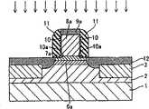
本实施方式的双极晶体管是基极由SiGe合金构成的NPN型的异质结双极晶体管。如图1及图2所示,该双极晶体管中,在p型硅衬底1上形成有集电极层2。集电极层2通过在硅衬底1上外延成长n型硅而形成。在该集电极层2的局部形成有由STI构成的元件分离层3。集电极层2中被元件分离层3包围的区域为活性区域。The bipolar transistor of this embodiment is an NPN type heterojunction bipolar transistor whose base is made of a SiGe alloy. As shown in FIGS. 1 and 2 , in this bipolar transistor, a
在集电极层2的活性区域上形成有由p型的SiGe合金层6a和具有凸状的截面形状的p型硅膜7a构成的导电层。SiGe合金层的带隙比硅膜的带隙窄。在硅膜7a内的上部形成有作为发射极层起作用的n型的发射极扩散层13。由SiGe合金层6a和硅膜7a中未扩散n型杂质的区域构成基极层。在发射极扩散层13上形成有n型的多晶硅膜8a。在多晶硅膜8a上形成有氮化硅膜9a。另外,硅膜7a包含与多晶硅膜8a具有同一宽度的上侧部分7b和具有比多晶硅膜8a的宽度大的宽度的下侧部分7c。由上侧部分7b和下侧部分7c形成台阶7d。另外,多晶硅膜8a是本发明的“发射极电极”之一例。另外,SiGe合金层6a是本发明的“窄带隙区域”之一例。A conductive layer composed of a p-type
本实施方式中,在多晶硅膜8a的侧面和硅膜7a的表面形成有绝缘膜10。另外,沿多晶硅膜8a与硅膜7a的界面50设有自多晶硅膜8a的外侧向内侧突出的由氧化硅膜构成的突出部10a(突出量L)。绝缘膜10和突出部10a一体地形成。在此,硅膜7a与多晶硅膜8a的界面50位于绝缘膜10的下面60(硅膜7a的第一部分7b与第二部分7c的台阶7d)的上方。因此,硅膜7a内的发射极扩散层13(发射极层)的沿界面50的方向的宽度W2比多晶硅膜8a的沿界面50的方向的宽度W1(硅膜7a的第一部分7b的沿界面50的方向的宽度W1)小。In this embodiment,
另外,按照覆盖绝缘膜10的表面及氮化硅膜9a的侧面的方式形成有由绝缘膜构成的侧壁膜11。而且,在侧壁膜11的外侧的区域形成有作为外部基极层使用的p型外部基极扩散层12。In addition, a
其次,参照图1~图7说明本实施方式的双极晶体管的制造工艺。Next, a manufacturing process of the bipolar transistor of this embodiment will be described with reference to FIGS. 1 to 7 .
如图3所示,首先,使用公知的技术在p型硅衬底1上外延成长n型硅,由此形成作为集电极层2的外延层。然后,在集电极层2的局部形成由STI构成的元件分离层3。另外,也可以采用由LOCOS(Local Oxidation of Silicon:硅的局部氧化)膜构成的元件分离层来代替由STI构成的元件分离层3。其次,使用减压CVD(Chemical Vapor Deposition:化学气相沉积)法使掺杂了p型杂质的SiGe合金层6及不含锗(Ge)的硅膜7分别外延成长。之后,利用减压CVD法层叠掺杂了高浓度的n型杂质的多晶硅膜8。另外,在多晶硅膜8上层叠氮化硅膜9。然后,利用平版印刷法形成用于将多晶硅膜8加工成所希望的发射极电极的规定图案的抗蚀剂掩模PR。As shown in FIG. 3 , first, n-type silicon is epitaxially grown on p-
其次,如图4所示,利用干式蚀刻将氮化硅膜9作为氮化硅膜9a进行加工。氮化硅膜9a作为蚀刻加工多晶硅膜8时的掩模起作用。其次,按顺序干式蚀刻多晶硅膜8及硅膜7。此时,干式蚀刻在完全除去硅膜7之前不进行,而以在SiGe合金层6上的整个面上残留硅膜7的一部分的状态结束。其结果是,硅膜7形成具有由第一部分7b、第二部分7c及台阶7d构成的凸状的截面形状的硅膜7a。此时,在硅膜7a的表面有蚀刻损伤,形成损伤层(未图示)。另外,多晶硅膜8被加工成作为发射极电极起作用的多晶硅膜8a。Next, as shown in FIG. 4, silicon nitride film 9 is processed as
其次,如图5所示,通过使用热氧化法对多晶硅膜8a的侧面及硅膜7a的表面进行热氧化,形成由氧化硅膜构成的绝缘膜10。另外,在形成绝缘膜10的同时,沿多晶硅膜8a与硅膜7a的界面50形成自多晶硅膜8a的外侧向内侧突出的由氧化硅膜构成的突出部10a(突出量L)。作为热氧化的条件,例如使用已有的RTO(Rapid Thermal Oxidation:快速热氧化)装置在O2环境中以900℃左右进行10秒左右。由此,在多晶硅膜8a的侧面及硅膜7a的表面形成作为绝缘膜10的5~15nm左右的热氧化膜。另外,沿多晶硅膜8a与硅膜7a的界面50形成自多晶硅膜8a的外侧具有1~5nm左右的突出量L的由氧化硅膜构成的突缘状的突出部10a。另外,在上述RTO的条件下,多晶硅膜8a中的n型杂质几乎不向硅膜7a扩散。Next, as shown in FIG. 5, the side surfaces of the
其次,如图6所示,使用CVD法在整个面上层叠氧化硅膜,同时进行干式蚀刻,由此反复蚀刻其整个面。由此,形成被称作侧壁的由氧化硅膜构成的侧壁膜11,使其覆盖氮化硅膜9a的侧面及绝缘膜10的侧面。此时,将形成于硅膜7a的表面的热氧化膜即绝缘膜10的不需要的部分除去。Next, as shown in FIG. 6, a silicon oxide film is laminated on the entire surface using the CVD method, and dry etching is performed simultaneously, thereby repeatedly etching the entire surface. Thus, a
其次,如图7所示,以氮化硅膜9a及侧壁膜11为掩模,使用离子注入法注入p型杂质,之后利用热处理进行活化。由此,在侧壁膜11的外侧的区域形成作为外部基极层起作用的p型的外部基极扩散层12。在此,SiGe合金层6中未注入p型杂质的区域成为SiGe合金层6a。该离子注入方面,通过设定离子不通过多晶硅膜8a上存在的氮化硅膜9a的条件,可不向多晶硅膜8a注入p型杂质。Next, as shown in FIG. 7, using the
其次,如图1所示,通过进行热处理,使多晶硅膜8a中的n型杂质向硅膜7a扩散。由此,形成作为发射极层起作用的n型的发射极扩散层13。其结果是,在硅膜7a内形成含n型杂质的区域(发射极扩散层13)和不含n型杂质的区域,并且,在硅膜7a内形成发射极-基极结。另外,热处理是使用RTA(Rapid Thermal Anneal:快速热退火)装置以1050℃左右进行5~30秒左右的热处理。Next, as shown in FIG. 1, n-type impurities in
在此,在本实施方式中,在通过自多晶硅膜8a的扩散n型杂质而形成发射极扩散层13时,沿界面50形成的突出部10a成为n型杂质的扩散势垒,由此限制n型杂质向硅膜7a内的扩散。由此,可将多晶硅膜8a中易形成发射极扩散层13的部分的宽度减小突出部10a突出的量。Here, in this embodiment, when the
另外,在进行热扩散时,对具有凸状的截面形状的硅膜7a的表面(第一部分7b的侧面及第二部分7c的上面(参照图2))施加的蚀刻损伤(损伤层)在形成侧壁膜11后也还有残留。在这样的损伤层内,n型杂质的固相扩散速度加快。因此,如现有构造的情况(没有突出部的情况),在损伤层上有n型杂质扩散的情况下,由于在损伤层n型杂质大范围扩散,故发射极层的厚度不均匀。与此同时,由于在损伤层部分基极层相对薄,故击穿电压降低,因此,可能不能得到规定的晶体管动作。与之相对,在沿界面50设置了突出部10a的情况下,通过按照覆盖损伤层的方式调节突出部10a的突出量L,能够抑制n型杂质向损伤层内的扩散。In addition, during thermal diffusion, etching damage (damaged layer) applied to the surface of the
其次,图中未图示,在半导体衬底的表面堆积绝缘膜。然后,在该绝缘膜的与集电极层、外部基极层及发射极电极分别对应的区域形成用于进行接触的开口。之后,经由各区域的开口形成与集电极层、外部基极层及发射极电极分别连接的端子,由此制造本实施方式的双极晶体管(半导体装置)。Next, not shown in the drawing, an insulating film is deposited on the surface of the semiconductor substrate. Then, openings for making contacts are formed in regions of the insulating film corresponding to the collector layer, the extrinsic base layer, and the emitter electrode, respectively. Thereafter, terminals connected to the collector layer, the external base layer, and the emitter electrode are formed through openings in the respective regions, whereby the bipolar transistor (semiconductor device) of this embodiment is manufactured.
在本实施方式中,如上所述,通过形成自发射极电极(多晶硅膜8a)的外侧向内侧突出的突出部10a,可抑制在使杂质自发射极电极向硅膜7a扩散时,杂质向与形成有突出部10a的部分对应的硅膜7a的部分扩散。因此,可使发射极扩散层13的沿界面50的方向的宽度W2减小突出部10a的突出长度L的量。由此,即使不设置高精度的曝光装置以减小发射极电极(多晶硅膜8a)的宽度,也能够减小发射极扩散层13的沿界面50的方向的宽度。因此,可不设置高精度的曝光装置而制造高性能化的双极晶体管。In the present embodiment, as described above, by forming the protruding
另外,在本实施方式中,如上所述,通过形成突出部10a,可通过突出部10a抑制n型杂质向损伤层内的扩散。由此,可减小发射极层(发射极扩散层13)的厚度及宽度的偏差,因此,可得到性能偏差小的双极晶体管。In addition, in the present embodiment, as described above, by forming the protruding
此外,在本实施方式中,如上所述,通过设定使发射极层(发射极扩散层13)的沿界面50的方向的宽度W2比发射极电极(多晶硅膜8a)的沿界面50的方向的宽度W1小,与目前相比,可用少的电流得到相同的电流密度,并且可得到高的电流放大率。因此,可得到耗电量低的双极晶体管。In addition, in the present embodiment, as described above, by setting the width W2 of the emitter layer (emitter diffusion layer 13) along the
另外,在本实施方式中,如上所述,通过利用采用了已有的热处理装置的热处理在界面50形成突出部10a,可不设置高精度的曝光装置而减小多晶硅膜8a的易形成发射极扩散层13的部分的宽度。由此,可以以低成本制造发射极层(发射极扩散层13)的沿界面50的方向的宽度W2减小了的双极晶体管。In addition, in the present embodiment, as described above, by forming the protruding
另外,在本实施方式中,如上所述,通过使用热处理法沿界面50使氧化膜成长来形成突出部10a,从而工艺上稳定,且可容易地减小多晶硅膜8a的易形成发射极扩散层13的部分的宽度。In addition, in this embodiment, as described above, the protruding
另外,本次公开的实施方式是以所有点进行的示例,应认为并不是对本发明进行限制。本发明的范围不是由上述实施方式的说明,而由权利要求的范围表示,进而包含与权利要求的范围均等的意思及范围内的所有变更。In addition, the embodiment disclosed this time is an illustration at every point, and it should not be thought that it limits this invention. The scope of the present invention is shown not by the description of the above-mentioned embodiment but by the scope of the claims, and further includes all changes within the meaning and range equivalent to the scope of the claims.
例如,在上述实施方式中,表示了本发明适用于NPN型双极晶体管的例子,但本发明不限于此,也可以将本发明应用于使各区域的导电型反向的PNP型双极晶体管。For example, in the above-mentioned embodiments, an example in which the present invention is applied to an NPN type bipolar transistor is shown, but the present invention is not limited to this, and the present invention can also be applied to a PNP type bipolar transistor in which the conductivity type of each region is reversed. .
另外,在上述实施方式中,表示了通过在硅衬底1上层叠由硅构成的外延层而形成集电极层2的例子,但本发明不限于此,也可以自p型或n型硅的硅衬底1的表面离子注入与其极性相反的杂质,而形成集电极层。In addition, in the above-mentioned embodiment, an example was shown in which the
此外,在上述实施方式中,表示了作为发射极层使用的发射极扩散层13的下面位于硅膜7a内的例子,但本发明不限于此。例如图8所示的变形例的半导体装置,通过减薄硅膜7a的厚度等,也可以使发射极扩散层13a的下面达到SiGe合金层6a中。据此,与上述实施方式(未达到SiGe合金层6中的情况)相比,可缩短自发射极扩散层13a的下面到活性区域(集电极层2)的距离。由此,可缩短自发射极层侧流向集电极层的电子的移动时间,因此可形成高速动作的晶体管。In addition, in the above-mentioned embodiment, an example was shown in which the lower surface of the
另外,在发射极扩散层13a的下面处于SiGe合金层6a中的情况下,SiGe合金层的带隙比硅膜的带隙窄,因此,相对于自发射极层(发射极扩散层13a)向基极层(SiGe合金层6a)注入的电子的势垒高度减小。由此,发射极注入效率大,可得到更高的电流放大率。In addition, when the lower surface of the
Claims (20)
Applications Claiming Priority (2)
| Application Number | Priority Date | Filing Date | Title |
|---|---|---|---|
| JP048254/07 | 2007-02-28 | ||
| JP2007048254AJP2008211105A (en) | 2007-02-28 | 2007-02-28 | Semiconductor device and manufacturing method thereof |
Publications (1)
| Publication Number | Publication Date |
|---|---|
| CN101257043Atrue CN101257043A (en) | 2008-09-03 |
Family
ID=39773800
Family Applications (1)
| Application Number | Title | Priority Date | Filing Date |
|---|---|---|---|
| CNA2008100806629APendingCN101257043A (en) | 2007-02-28 | 2008-02-28 | Semiconductor device and manufacturing method thereof |
Country Status (3)
| Country | Link |
|---|---|
| US (1) | US20080230809A1 (en) |
| JP (1) | JP2008211105A (en) |
| CN (1) | CN101257043A (en) |
Cited By (2)
| Publication number | Priority date | Publication date | Assignee | Title |
|---|---|---|---|---|
| CN107342319A (en)* | 2017-06-21 | 2017-11-10 | 燕山大学 | A kind of composite strain Si/SiGe heterojunction bipolar transistors and preparation method thereof |
| CN110120344A (en)* | 2019-04-09 | 2019-08-13 | 上海华虹宏力半导体制造有限公司 | A method of self-alignment structure is realized with silicon nitride spacer in germanium silicium HBT |
Family Cites Families (1)
| Publication number | Priority date | Publication date | Assignee | Title |
|---|---|---|---|---|
| JP4775688B2 (en)* | 2004-07-16 | 2011-09-21 | オンセミコンダクター・トレーディング・リミテッド | Semiconductor device |
- 2007
- 2007-02-28JPJP2007048254Apatent/JP2008211105A/enactivePending
- 2008
- 2008-02-28CNCNA2008100806629Apatent/CN101257043A/enactivePending
- 2008-02-28USUS12/073,053patent/US20080230809A1/ennot_activeAbandoned
Cited By (4)
| Publication number | Priority date | Publication date | Assignee | Title |
|---|---|---|---|---|
| CN107342319A (en)* | 2017-06-21 | 2017-11-10 | 燕山大学 | A kind of composite strain Si/SiGe heterojunction bipolar transistors and preparation method thereof |
| CN107342319B (en)* | 2017-06-21 | 2019-12-10 | 燕山大学 | A compound strained Si/SiGe heterojunction bipolar transistor and its preparation method |
| CN110120344A (en)* | 2019-04-09 | 2019-08-13 | 上海华虹宏力半导体制造有限公司 | A method of self-alignment structure is realized with silicon nitride spacer in germanium silicium HBT |
| CN110120344B (en)* | 2019-04-09 | 2022-08-16 | 上海华虹宏力半导体制造有限公司 | Method for realizing self-alignment structure by using silicon nitride side wall in germanium-silicon Heterojunction Bipolar Transistor (HBT) |
Also Published As
| Publication number | Publication date |
|---|---|
| JP2008211105A (en) | 2008-09-11 |
| US20080230809A1 (en) | 2008-09-25 |
Similar Documents
| Publication | Publication Date | Title |
|---|---|---|
| JP3544833B2 (en) | Semiconductor device and manufacturing method thereof | |
| JP3494638B2 (en) | Semiconductor device and method of manufacturing semiconductor device | |
| KR100486304B1 (en) | Method for manufacturing self-aligned BiCMOS | |
| US20060226446A1 (en) | Bipolar transistor and method for fabricating the same | |
| JP2010010456A (en) | Semiconductor device | |
| KR100554465B1 (en) | Silicon wafer silicon element embodied on a SOI substrate and a method of manufacturing the same | |
| JP2002289834A (en) | Semiconductor device manufacturing method and semiconductor device | |
| US20060121667A1 (en) | Method of fabricating SiGe Bi-CMOS device | |
| JP2007299890A (en) | Manufacturing method of semiconductor device | |
| US7198998B2 (en) | Method of manufacturing bipolar-complementary metal oxide semiconductor | |
| CN101257043A (en) | Semiconductor device and manufacturing method thereof | |
| JP3732814B2 (en) | Semiconductor device | |
| JP4775688B2 (en) | Semiconductor device | |
| CN1957461A (en) | Semiconductor device and manufacturing method thereof | |
| JP2006128628A (en) | Semiconductor device | |
| JP5547516B2 (en) | Manufacturing method of semiconductor device | |
| JP3908023B2 (en) | Manufacturing method of semiconductor device | |
| US7170113B2 (en) | Semiconductor device and method of manufacturing the same | |
| JPH11307771A (en) | Semiconductor device and manufacturing method thereof | |
| US20060170074A1 (en) | Semiconductor device | |
| JP4714564B2 (en) | Manufacturing method of semiconductor device | |
| JP4458895B2 (en) | Bipolar transistor | |
| CN101304030A (en) | Semiconductor device and manufacturing method thereof | |
| JP2001015524A (en) | Method for manufacturing semiconductor device | |
| US20040126979A1 (en) | Bipolar transistor and method of manufacturing the same |
Legal Events
| Date | Code | Title | Description |
|---|---|---|---|
| C06 | Publication | ||
| PB01 | Publication | ||
| C02 | Deemed withdrawal of patent application after publication (patent law 2001) | ||
| WD01 | Invention patent application deemed withdrawn after publication | Open date:20080903 |