CN101256310B - Backlight unit having light emitting diodes and method of manufacturing the same - Google Patents
Backlight unit having light emitting diodes and method of manufacturing the sameDownload PDFInfo
- Publication number
- CN101256310B CN101256310BCN2008100827184ACN200810082718ACN101256310BCN 101256310 BCN101256310 BCN 101256310BCN 2008100827184 ACN2008100827184 ACN 2008100827184ACN 200810082718 ACN200810082718 ACN 200810082718ACN 101256310 BCN101256310 BCN 101256310B
- Authority
- CN
- China
- Prior art keywords
- chassis
- insulating layer
- backlight unit
- circuit pattern
- light emitting
- Prior art date
- Legal status (The legal status is an assumption and is not a legal conclusion. Google has not performed a legal analysis and makes no representation as to the accuracy of the status listed.)
- Active
Links
Images


Classifications
- H—ELECTRICITY
- H05—ELECTRIC TECHNIQUES NOT OTHERWISE PROVIDED FOR
- H05K—PRINTED CIRCUITS; CASINGS OR CONSTRUCTIONAL DETAILS OF ELECTRIC APPARATUS; MANUFACTURE OF ASSEMBLAGES OF ELECTRICAL COMPONENTS
- H05K1/00—Printed circuits
- H05K1/02—Details
- H05K1/03—Use of materials for the substrate
- H05K1/05—Insulated conductive substrates, e.g. insulated metal substrate
- H05K1/053—Insulated conductive substrates, e.g. insulated metal substrate the metal substrate being covered by an inorganic insulating layer
- G—PHYSICS
- G02—OPTICS
- G02F—OPTICAL DEVICES OR ARRANGEMENTS FOR THE CONTROL OF LIGHT BY MODIFICATION OF THE OPTICAL PROPERTIES OF THE MEDIA OF THE ELEMENTS INVOLVED THEREIN; NON-LINEAR OPTICS; FREQUENCY-CHANGING OF LIGHT; OPTICAL LOGIC ELEMENTS; OPTICAL ANALOGUE/DIGITAL CONVERTERS
- G02F1/00—Devices or arrangements for the control of the intensity, colour, phase, polarisation or direction of light arriving from an independent light source, e.g. switching, gating or modulating; Non-linear optics
- G02F1/01—Devices or arrangements for the control of the intensity, colour, phase, polarisation or direction of light arriving from an independent light source, e.g. switching, gating or modulating; Non-linear optics for the control of the intensity, phase, polarisation or colour
- G02F1/13—Devices or arrangements for the control of the intensity, colour, phase, polarisation or direction of light arriving from an independent light source, e.g. switching, gating or modulating; Non-linear optics for the control of the intensity, phase, polarisation or colour based on liquid crystals, e.g. single liquid crystal display cells
- G02F1/133—Constructional arrangements; Operation of liquid crystal cells; Circuit arrangements
- G02F1/1333—Constructional arrangements; Manufacturing methods
- G02F1/1335—Structural association of cells with optical devices, e.g. polarisers or reflectors
- G02F1/1336—Illuminating devices
- G02F1/133602—Direct backlight
- G02F1/133603—Direct backlight with LEDs
- G—PHYSICS
- G02—OPTICS
- G02F—OPTICAL DEVICES OR ARRANGEMENTS FOR THE CONTROL OF LIGHT BY MODIFICATION OF THE OPTICAL PROPERTIES OF THE MEDIA OF THE ELEMENTS INVOLVED THEREIN; NON-LINEAR OPTICS; FREQUENCY-CHANGING OF LIGHT; OPTICAL LOGIC ELEMENTS; OPTICAL ANALOGUE/DIGITAL CONVERTERS
- G02F1/00—Devices or arrangements for the control of the intensity, colour, phase, polarisation or direction of light arriving from an independent light source, e.g. switching, gating or modulating; Non-linear optics
- G02F1/01—Devices or arrangements for the control of the intensity, colour, phase, polarisation or direction of light arriving from an independent light source, e.g. switching, gating or modulating; Non-linear optics for the control of the intensity, phase, polarisation or colour
- G02F1/13—Devices or arrangements for the control of the intensity, colour, phase, polarisation or direction of light arriving from an independent light source, e.g. switching, gating or modulating; Non-linear optics for the control of the intensity, phase, polarisation or colour based on liquid crystals, e.g. single liquid crystal display cells
- G02F1/133—Constructional arrangements; Operation of liquid crystal cells; Circuit arrangements
- G02F1/1333—Constructional arrangements; Manufacturing methods
- G02F1/1335—Structural association of cells with optical devices, e.g. polarisers or reflectors
- G02F1/1336—Illuminating devices
- G02F1/133602—Direct backlight
- G02F1/133612—Electrical details
- H—ELECTRICITY
- H05—ELECTRIC TECHNIQUES NOT OTHERWISE PROVIDED FOR
- H05K—PRINTED CIRCUITS; CASINGS OR CONSTRUCTIONAL DETAILS OF ELECTRIC APPARATUS; MANUFACTURE OF ASSEMBLAGES OF ELECTRICAL COMPONENTS
- H05K1/00—Printed circuits
- H05K1/02—Details
- H05K1/09—Use of materials for the conductive, e.g. metallic pattern
- H05K1/092—Dispersed materials, e.g. conductive pastes or inks
- H—ELECTRICITY
- H05—ELECTRIC TECHNIQUES NOT OTHERWISE PROVIDED FOR
- H05K—PRINTED CIRCUITS; CASINGS OR CONSTRUCTIONAL DETAILS OF ELECTRIC APPARATUS; MANUFACTURE OF ASSEMBLAGES OF ELECTRICAL COMPONENTS
- H05K2201/00—Indexing scheme relating to printed circuits covered by H05K1/00
- H05K2201/10—Details of components or other objects attached to or integrated in a printed circuit board
- H05K2201/10007—Types of components
- H05K2201/10106—Light emitting diode [LED]
- H—ELECTRICITY
- H05—ELECTRIC TECHNIQUES NOT OTHERWISE PROVIDED FOR
- H05K—PRINTED CIRCUITS; CASINGS OR CONSTRUCTIONAL DETAILS OF ELECTRIC APPARATUS; MANUFACTURE OF ASSEMBLAGES OF ELECTRICAL COMPONENTS
- H05K2203/00—Indexing scheme relating to apparatus or processes for manufacturing printed circuits covered by H05K3/00
- H05K2203/01—Tools for processing; Objects used during processing
- H05K2203/0104—Tools for processing; Objects used during processing for patterning or coating
- H05K2203/013—Inkjet printing, e.g. for printing insulating material or resist
- H—ELECTRICITY
- H05—ELECTRIC TECHNIQUES NOT OTHERWISE PROVIDED FOR
- H05K—PRINTED CIRCUITS; CASINGS OR CONSTRUCTIONAL DETAILS OF ELECTRIC APPARATUS; MANUFACTURE OF ASSEMBLAGES OF ELECTRICAL COMPONENTS
- H05K3/00—Apparatus or processes for manufacturing printed circuits
- H05K3/10—Apparatus or processes for manufacturing printed circuits in which conductive material is applied to the insulating support in such a manner as to form the desired conductive pattern
- H05K3/12—Apparatus or processes for manufacturing printed circuits in which conductive material is applied to the insulating support in such a manner as to form the desired conductive pattern using thick film techniques, e.g. printing techniques to apply the conductive material or similar techniques for applying conductive paste or ink patterns
- H05K3/1216—Apparatus or processes for manufacturing printed circuits in which conductive material is applied to the insulating support in such a manner as to form the desired conductive pattern using thick film techniques, e.g. printing techniques to apply the conductive material or similar techniques for applying conductive paste or ink patterns by screen printing or stencil printing
- H—ELECTRICITY
- H05—ELECTRIC TECHNIQUES NOT OTHERWISE PROVIDED FOR
- H05K—PRINTED CIRCUITS; CASINGS OR CONSTRUCTIONAL DETAILS OF ELECTRIC APPARATUS; MANUFACTURE OF ASSEMBLAGES OF ELECTRICAL COMPONENTS
- H05K3/00—Apparatus or processes for manufacturing printed circuits
- H05K3/10—Apparatus or processes for manufacturing printed circuits in which conductive material is applied to the insulating support in such a manner as to form the desired conductive pattern
- H05K3/12—Apparatus or processes for manufacturing printed circuits in which conductive material is applied to the insulating support in such a manner as to form the desired conductive pattern using thick film techniques, e.g. printing techniques to apply the conductive material or similar techniques for applying conductive paste or ink patterns
- H05K3/1241—Apparatus or processes for manufacturing printed circuits in which conductive material is applied to the insulating support in such a manner as to form the desired conductive pattern using thick film techniques, e.g. printing techniques to apply the conductive material or similar techniques for applying conductive paste or ink patterns by ink-jet printing or drawing by dispensing
- H05K3/125—Apparatus or processes for manufacturing printed circuits in which conductive material is applied to the insulating support in such a manner as to form the desired conductive pattern using thick film techniques, e.g. printing techniques to apply the conductive material or similar techniques for applying conductive paste or ink patterns by ink-jet printing or drawing by dispensing by ink-jet printing
Landscapes
- Physics & Mathematics (AREA)
- Nonlinear Science (AREA)
- Chemical & Material Sciences (AREA)
- Crystallography & Structural Chemistry (AREA)
- Microelectronics & Electronic Packaging (AREA)
- Mathematical Physics (AREA)
- Engineering & Computer Science (AREA)
- Inorganic Chemistry (AREA)
- General Physics & Mathematics (AREA)
- Optics & Photonics (AREA)
- Led Device Packages (AREA)
- Planar Illumination Modules (AREA)
- Led Devices (AREA)
- Liquid Crystal (AREA)
- Fastening Of Light Sources Or Lamp Holders (AREA)
Abstract
Translated fromChinese
Description
Translated fromChinese相关申请交叉参考Related Application Cross Reference
本申请要求于2007年2月27日向韩国知识产权局提交的No.2007-0019863韩国专利申请的优先权,其公开内容结合于此进行参考。This application claims priority from Korean Patent Application No. 2007-0019863 filed with the Korean Intellectual Property Office on February 27, 2007, the disclosure of which is incorporated herein by reference.
技术领域technical field
本发明涉及用于使用发光二极管的液晶显示器的背光单元及其制造方法,并且更特别地,涉及这样一种背光单元,该背光组件的零件(诸如印刷电路板(PCB)、用于连接其上安装有发光二极管的PCB的连接件、以及用于固定PCB的结构)数目显著减少,并且制造和组装过程简化了,还涉及制造该背光单元的方法。The present invention relates to a backlight unit for a liquid crystal display using light emitting diodes and a method of manufacturing the same, and more particularly, to a backlight unit in which parts such as a printed circuit board (PCB) for connection thereon The number of connectors of the PCB on which the light emitting diodes are installed, and the structure for fixing the PCB) is significantly reduced, and the manufacturing and assembly processes are simplified, and also relates to a method of manufacturing the backlight unit.
背景技术Background technique
随着近来显示装置更薄且性能更高的趋势,液晶显示器广泛的应用在TV和监控器中。液晶显示面板自身不发射光线,因此需要额外的背光单元(BLU)。使用冷阴极荧光灯(CCFL)的传统BLU在水银诱发的环境污染、低响应速率以及难以部分驱动等方面是很不利的。为了克服这些问题,已经提出用发光二极管(LED)取代CCFL作为BLU光源。这个基于LED的BLU可实现高色彩再现性,并且是对环境有利的且通过局部减低亮度驱动。With the recent trend of thinner display devices and higher performance, liquid crystal displays are widely used in TVs and monitors. The LCD panel itself does not emit light, so an additional backlight unit (BLU) is required. Conventional BLUs using cold-cathode fluorescent lamps (CCFLs) are disadvantageous in terms of mercury-induced environmental pollution, low response rate, and difficult to drive partially. To overcome these problems, it has been proposed to replace CCFLs with light emitting diodes (LEDs) as the BLU light source. This LED-based BLU achieves high color rendition and is environmentally friendly and driven by local dimming.
BLU包括直下式(direct-type)BLU和边缘型(edge-type)BLU。在边缘型BLU中,将条形光源设置在液晶显示面板的边缘处以通过导光板将光发射到液晶显示面板上。另一方面,在直下式BLU中,将使用LED的面光源设置在液晶显示面板的下方以直接将光发射到其上。The BLU includes a direct-type BLU and an edge-type BLU. In an edge type BLU, a bar-shaped light source is disposed at an edge of a liquid crystal display panel to emit light onto the liquid crystal display panel through a light guide plate. On the other hand, in the direct type BLU, a surface light source using LEDs is disposed below the liquid crystal display panel to directly emit light thereon.
单个LED对应于点光源且具有低的光通量。因此,为了生产在大的LCD-TV中使用的直下式BLU,通常将成百上千个LED安装在分割开的PCB上并且随后连接至底架结构(chassis structure)。为了加强直下式BLU的机械稳定性和发光性能,需要诸如螺钉和间隙垫(gap pads)的零件并且用于电连接PCB的连接件是必需的。A single LED corresponds to a point light source and has a low luminous flux. Therefore, to produce direct-lit BLUs used in large LCD-TVs, typically hundreds or thousands of LEDs are mounted on separate PCBs and then connected to a chassis structure. In order to enhance mechanical stability and light emitting performance of the direct type BLU, parts such as screws and gap pads are required and connectors for electrically connecting PCBs are necessary.
图1示意性地示出了传统的BLU,其中图1A是横截面图,图1B是平面图。参照图1,BLU 10包括其上安装有多个LED 25的PCB 21、底架11、以及其它光学片(sheet)33,诸如与PCB 21分离开的漫射板31和棱镜。将液晶显示面板40设置在BLU上方以接收从BLU 10发射的白色表面光。其上安装有LED 25的PCB 21构成BLU的光源部件。FIG. 1 schematically shows a conventional BLU, wherein FIG. 1A is a cross-sectional view and FIG. 1B is a plan view. Referring to FIG. 1, the BLU 10 includes a
如图1A和1B中所示,将LED 25(即,点光源)安装在作为芯片或是在封装件中的间隔开的PCB上。将PCB 21固定至位于PCB下方的金属材料的底部底架(简单地,称“底架”)。为了平稳地放射从LED 25发射的热,可以在底架11与PCB 21之间设置间隙垫22。需要诸如螺钉的连接单元以将PCB 21固定至底架11。此外,间隔开的PCB 21可以通过连接件23彼此电连接。As shown in FIGS. 1A and 1B , LEDs 25 (ie, point sources of light) are mounted on spaced apart PCBs either as chips or in packages. The PCB 21 is secured to the bottom chassis (simply, the "chassis") of the metal material located below the PCB. In order to smoothly radiate heat emitted from the
为了制造传统的BLU 10,使用诸如螺钉的连接单元将PCB 21固定至底架11。这使得组装过程不但耗时而且效率低。并且,用于通过连接件将分离的PCB 21彼此连接的组装过程需要相当多的资源和时间。此外,LED 25产生的热量通过PCB 21和昂贵的间隙垫22向外散发,因而导致高的材料成本和不充足的散热特性。To manufacture a conventional BLU 10, the PCB 21 is fixed to the
发明内容Contents of the invention
本发明的一个方面提供一种具有LED的背光单元,该背光单元可以以简单的方式方便地组装,并降低包括材料成本的制造成本,且增加散发效率。An aspect of the present invention provides a backlight unit having LEDs, which can be conveniently assembled in a simple manner, reduces manufacturing costs including material costs, and increases emission efficiency.
本发明的一个方面还提供了一种制造具有LED的背光单元的方法,其中,该背光单元可以以更简单的工艺制造,且时间更短,成本低。An aspect of the present invention also provides a method of manufacturing a backlight unit having LEDs, wherein the backlight unit can be manufactured in a simpler process with shorter time and low cost.
根据本发明的一个方面,提供了一种背光单元,其包括:底架,具有形成在其顶部的绝缘层;电路图案,在绝缘层上形成;多个发光二极管(LED),在绝缘层上形成以电连接至电路图案。According to an aspect of the present invention, there is provided a backlight unit comprising: a chassis having an insulating layer formed on top thereof; a circuit pattern formed on the insulating layer; a plurality of light emitting diodes (LEDs) formed on the insulating layer formed to be electrically connected to the circuit pattern.
背光单元可以进一步包括形成在底架的底部上的另一绝缘层。多个LED可以是白光LED。多个LED可以包括蓝光LED、绿光LED和红光LED。The backlight unit may further include another insulating layer formed on the bottom of the chassis. The plurality of LEDs may be white LEDs. The plurality of LEDs may include blue LEDs, green LEDs, and red LEDs.
底架可以由铝和铝合金之一形成。绝缘层可以是铝阳极氧化层(aluminum anodized layer)。The chassis may be formed of one of aluminum and an aluminum alloy. The insulating layer may be an aluminum anodized layer.
电路图案可以由包含银(Ag)的材料形成。电路图案可以由银膏的烧结材料形成。The circuit pattern may be formed of a material including silver (Ag). The circuit pattern may be formed of a sintered material of silver paste.
根据本发明的另一个方面,提供了一种制造背光单元的方法,此方法包括:准备底架;在底架的顶部上形成绝缘层;在绝缘层上形成电路图案;以及将多个LED安装在绝缘层上以连接至电路图案。According to another aspect of the present invention, there is provided a method of manufacturing a backlight unit, the method comprising: preparing a chassis; forming an insulating layer on top of the chassis; forming a circuit pattern on the insulating layer; and mounting a plurality of LEDs On the insulating layer to connect to the circuit pattern.
底架可以由铝和铝合金之一形成。在底架的顶部上形成绝缘层可以包括阳极氧化底架的顶部以在底架的顶部上形成铝阳极氧化层。The chassis may be formed of one of aluminum and an aluminum alloy. Forming the insulating layer on the top of the chassis may include anodizing the top of the chassis to form an aluminum anodized layer on the top of the chassis.
底架可以由铝和铝合金之一形成。在底架的顶部上形成绝缘层包括阳极氧化底架的顶部以在底架顶部上形成铝阳极氧化层。阳极氧化可以在底架的底部上进行。The chassis may be formed of one of aluminum and an aluminum alloy. Forming the insulating layer on the top of the chassis includes anodizing the top of the chassis to form an aluminum anodized layer on the top of the chassis. Anodizing can be performed on the bottom of the chassis.
形成电路图案可以包括:在底架顶部上的绝缘层上形成银膏;以及烧结银膏。形成银膏可以包括将银膏施加在绝缘层上。这里,可以通过丝网印刷和喷墨印刷之一来进行在绝缘层上施加银膏。Forming the circuit pattern may include: forming a silver paste on the insulating layer on top of the chassis; and sintering the silver paste. Forming the silver paste may include applying the silver paste on the insulating layer. Here, applying the silver paste on the insulating layer may be performed by one of screen printing and inkjet printing.
附图说明Description of drawings
从随后结合附图的详细说明中可以更清晰地理解本发明的上述和其它方面、特征以及其它优点,附图中:The above and other aspects, features and other advantages of the present invention can be more clearly understood from the subsequent detailed description in conjunction with the accompanying drawings, in which:
图1A是示出了使用LED的传统背光单元的横截面图,图1B是示出了图1A的背光单元的平面图;1A is a cross-sectional view showing a conventional backlight unit using LEDs, and FIG. 1B is a plan view showing the backlight unit of FIG. 1A;
图2是示出了根据本发明示例性实施例的背光单元的横截面图;2 is a cross-sectional view illustrating a backlight unit according to an exemplary embodiment of the present invention;
图3是示出了图2的背光单元的局部放大图;FIG. 3 is a partially enlarged view showing the backlight unit of FIG. 2;
图4是示出了根据本发明另一示例性实施例的背光单元的横截面图;以及4 is a cross-sectional view illustrating a backlight unit according to another exemplary embodiment of the present invention; and
图5A至图5E是用于解释制造根据本发明示例性实施例的背光单元的方法的横截面图。5A to 5E are cross-sectional views for explaining a method of manufacturing a backlight unit according to an exemplary embodiment of the present invention.
具体实施方式Detailed ways
现在将参照附图详细地描述本发明的示例性实施例。然而,本发明可以以多种不同的形式实施并且不应该被认为限于这里所述的实施例。更确切地,提供这些实施例以使该公开全面、完整,并且会将本发明的范围完全传达给本领域的技术人员。在图中,为了清晰起见可以放大外形和尺寸,并且从始至终使用相同的参考标号来指明相同或相似的零件。Exemplary embodiments of the present invention will now be described in detail with reference to the accompanying drawings. However, this invention may be embodied in many different forms and should not be construed as limited to the embodiments set forth herein. Rather, these embodiments are provided so that this disclosure will be thorough and complete, and will fully convey the scope of the invention to those skilled in the art. In the drawings, the outlines and dimensions may be exaggerated for clarity, and the same reference numerals will be used throughout to designate the same or like parts.
图2示出了根据本发明的示例性实施例的直下式背光单元的示意性横截面图,并且图3是图2的局部放大图。FIG. 2 illustrates a schematic cross-sectional view of a direct type backlight unit according to an exemplary embodiment of the present invention, and FIG. 3 is a partially enlarged view of FIG. 2 .
参照图2和图3,背光单元100包括金属材料的底架101、形成在底架顶部上的绝缘层102a、以及多个形成在绝缘层102a上的发光二极管(LED)125。在绝缘层102a上形成导电电路图案105以将LED 125彼此电连接。并且,在底架的底部上形成下部绝缘层102b并且该绝缘层由与绝缘层102a相同或不同的材料制成。每个LED 125构成点光源,而被布置的多个LED 125可以作为整体形成面光源。如图所示,与图1相反,背光单元100不包括其上安装有LED的额外印刷电路板(PCB)。可以将诸如漫射板和棱镜的各种光学片(未示出)以与LED 125距离预定距离地设置在LED 125上方。Referring to FIGS. 2 and 3, the
LED 125可以包括白光LED,例如,GaN基蓝光LED和黄色荧光粉(磷光体)的组合,GaN基蓝光LED与绿色荧光粉和红色荧光粉的组合,或者紫外线或近紫外(UV)LED与蓝色荧光粉和绿色荧光粉以及红色荧光粉的组合。可替换地,为了产生白色的输出光,LED 125可以包括蓝光LED、绿光LED和红光LED。每个LED 125可以安装在分离封装件中或者通过板上芯片(COB)方法安装,在该方法中,将LED芯片直接安装在绝缘层102a上。
底架可以由铝(Al)或铝合金制成。由铝或铝合金制成的底架可以容易地在它的表面上被阳极氧化。这使得绝缘层102a和102b,即,铝阳极氧化层(anodized aluminum oxide layer,阳极氧化铝层)分别在底架的顶部和底部上形成。然而,可用于本发明的绝缘层102a和102b不限于铝阳极氧化层。例如,绝缘层102a和102b可以采用诸如类似聚酰亚胺的聚合物、以及陶瓷的其它绝缘体。并且,可以通过物理和化学方法而非阳极氧化来形成绝缘层。The chassis may be made of aluminum (Al) or aluminum alloy. A chassis made of aluminum or an aluminum alloy can easily be anodized on its surface. This allows insulating
导电电路图案105将LED 125彼此电连接并且可以连接至驱动电路(未示出)。例如,可以通过将银(Ag)膏(糊)施加在绝缘层102a上并且随后烧结银膏来形成电路图案105。然而,本发明不限于此。例如,作为实现电路图案105的方式,可以在绝缘层上直接形成金属电路。The
在背光单元100中,与传统的背光单元(见图1)相反,电路图案直接形成在其上形成有绝缘层102a的底架101上,因此不需要其上安装有LED的额外PCB(见图1的参考标号11)。因此,这就不需要用于将分开的PCB彼此连接的连接件(见图1的参考标号23)和用于将PCB固定至底架的连接单元(诸如螺钉)。In the
因此,这节省了用于将LED安装于其上的PCB、用于将PCB彼此连接的连接件、以及诸如螺钉的连接单元所需的材料成本,显著地减少了零件的数量并相对简化了结构。此外,LED 125产生的热量通过绝缘层102a直接传输至金属材料的宽阔底架101,因此显著的提高了散热特性。传统地,来自LED的热量通过诸如PCB和间隙垫等结构散发至底架下方,因而无法保证充分的散热(heatradiation)。然而,根据本实施例,没有采用阻碍散热的零件并且热量直接传输到由导热材料(例如,铝或铝合金)制成的底架。这保证了优于传统背光单元的散热特性。此外,在BLU 100的制造过程中,不需要用于固定PCB的组装过程。这显著的简化了BLU的制造过程,因而降低了组装所需的劳动力成本。Therefore, this saves the PCB for mounting the LEDs thereon, the connection member for connecting the PCBs to each other, and the material cost required for connection units such as screws, significantly reduces the number of parts and relatively simplifies the structure . In addition, the heat generated by the
图4是示出了根据本发明另一个实施例的BLU的局部放大图。在图4的实施例中,没有形成下部绝缘层(见图2的参考标号102b)。例如,用抗蚀剂掩盖由铝材料制成的底架的底部,并随后将此底部阳极氧化以仅在底架101的顶部上形成绝缘层102a,即,阳极氧化层。如上所述,不会在底架的底部上形成绝缘层。电路图案105可以只在底架101的顶部上形成,因此不需要在底架的底部上形成绝缘层。也就是,可以在底架101的顶部上形成诸如聚合物膜的不同材料的绝缘层。FIG. 4 is a partially enlarged view showing a BLU according to another embodiment of the present invention. In the embodiment of FIG. 4, the lower insulating layer (see reference numeral 102b of FIG. 2) is not formed. For example, the bottom of the chassis made of an aluminum material is masked with a resist, and then this bottom is anodized to form the insulating
在下文中,将根据本发明的示例性实施例描述制造BLU的方法。Hereinafter, a method of manufacturing a BLU will be described according to an exemplary embodiment of the present invention.
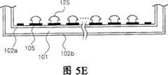
图5A至5B是用于解释制造本实施例的背光单元的方法的横截面图。首先,如图5A中所示,准备好由铝或铝合金制成的底架101。可以将底架101充分的弯曲以获得用于将多个LED放置在其上的空间。5A to 5B are cross-sectional views for explaining a method of manufacturing the backlight unit of the present embodiment. First, as shown in FIG. 5A, a
随后,如图5B中所示,通过对铝进行阳极氧化,在底架的顶部和底部上形成铝阳极氧化层102a和102b。可以控制诸如阳极氧化的时间、电压和所用电解液的成分(composition)的阳极氧化条件以使绝缘层(即,阳极氧化层102a和102b)形成至所需厚度。在阳极氧化过程中,可以用足够的绝缘体(例如,抗蚀剂膜)来掩盖不需要形成电路图案的底架的底部,以仅在底架的顶部上形成阳极氧化物层(见图4)。Subsequently, as shown in FIG. 5B, aluminum anodized
此后,如图5C中所示,将银膏105a施加在铝阳极氧化层102a上以形成电路图案。例如,可以通过丝网印刷和喷墨印刷中的一种施加银膏以形成电路图案。被印刷的银膏可以含有银粉和有机材料的混合物。随后,如图5D中所示,烧结银膏以形成所需的导电电路图案105。Thereafter, as shown in FIG. 5C, a
随后,如图5E中所示,将多个LED或LED封装件125安装在阳极氧化层102a上以连接至电路图案105。被安装的多个LED125可以是白光LED。例如,可以将GaN基蓝光LED芯片与含有黄色荧光粉(或红色和绿色荧光粉)的透光树脂封装到将被安装在阳极氧化层102a上的白光LED中。可替换地,可以将近UV LED芯片与含有蓝色荧光粉、绿色荧光粉和红色荧光粉的透光树脂封装到将被安装在阳极氧化层102a上的白光LED中。可替换地,可以将蓝光LED芯片或近UV LED芯片直接安装在阳极氧化层102a上以形成电路图案105,并且随后与含有适合的荧光粉或荧光粉混合物的树脂封装在一起。此外,LED 125可以包括蓝光LED、绿光LED和红光LED的组合。Subsequently, as shown in FIG. 5E , a plurality of LEDs or
制造本发明的背光单元的方法不限于图5A至图5E中所示的前述实施例。底架可以由取代铝或铝合金的其它材料制成。并且,绝缘层可以采用取代阳极氧化层的聚合物膜或二氧化硅膜。此外,电路图可以通过取代通过印刷和烧结银膏而施加银膏的方法的其它方法形成。例如,为了形成电路图案,可以直接在绝缘层上形成金属图案,或者可以形成金属层(铜膜)并随后将其图案化。The method of manufacturing the backlight unit of the present invention is not limited to the foregoing embodiments shown in FIGS. 5A to 5E . The chassis may be made of other materials instead of aluminum or aluminum alloys. Also, the insulating layer may use a polymer film or a silicon dioxide film instead of the anodized layer. In addition, the circuit pattern may be formed by other methods instead of the method of applying the silver paste by printing and firing the silver paste. For example, to form a circuit pattern, a metal pattern may be directly formed on an insulating layer, or a metal layer (copper film) may be formed and then patterned.
本背光单元的制造方法不需要采用诸如PCB、连接件、以及螺钉或连接单元的结构。本制造方法还除去了用于贴附间隙垫或通过螺钉将LED安装至底架的固定PCB的组装工序。因此,本制造方法比传统的制造方法显著地简化了,因而减少了交付周期并节省了组装过程所需的劳动力成本。这最终导致制造BLU中的更高的生产率。此外,BLU的传统组装过程需要相当多的手工劳动。但是根据本实施例的制造方法,可以使用LED装配机和回流焊机(reflowmachine,再流焊机)通过自动化方式简单地组装BLU。The manufacturing method of the present backlight unit does not need to employ structures such as PCBs, connectors, and screws or connection units. This manufacturing method also eliminates the assembly process for attaching gap pads or fixing the PCB to the chassis by screws. Therefore, the present manufacturing method is significantly simplified compared to conventional manufacturing methods, thereby reducing lead times and saving labor costs required for the assembly process. This ultimately leads to higher productivity in manufacturing BLUs. Furthermore, the traditional assembly process of BLU requires considerable manual labor. However, according to the manufacturing method of this embodiment, the BLU can be assembled simply and automatically by using an LED assembly machine and a reflow soldering machine (reflow machine, reflow soldering machine).
如上所述,根据本发明的示例性实施例,直接在具有形成在其顶部上的绝缘层的底架上形成电路图案,并且将LED安装在电路图案上。这不需要诸如PCB、连接件和螺钉的额外零件,因而节省了制造成本。并且,这增强了从LED生成的热量的散发(radiation)性能。在本BLU的制造方法中,不需要组装PCB。因此,与传统方法相比,本制造方法减少了所需要的工序数目,提高BLU的生产率,并且便于保证组装过程容易地实现自动化。As described above, according to an exemplary embodiment of the present invention, a circuit pattern is directly formed on a chassis having an insulating layer formed on top thereof, and LEDs are mounted on the circuit pattern. This does not require additional parts such as PCBs, connectors and screws, thus saving manufacturing costs. Also, this enhances the radiation performance of heat generated from the LED. In the manufacturing method of the present BLU, there is no need to assemble the PCB. Therefore, the present manufacturing method reduces the number of required processes, improves the productivity of the BLU, and facilitates the easy automation of the assembly process as compared with the conventional method.
尽管已经结合示例性实施例示出并描述了本发明,然而显而易见地,对于本领域的技术人员,在不背离所附权利要求所限定的本发明的精神和范围的前提下可以进行修改和变化。While the invention has been shown and described in conjunction with exemplary embodiments, it will be obvious to those skilled in the art that modifications and changes may be made without departing from the spirit and scope of the invention as defined in the appended claims.
Claims (13)
Translated fromChineseApplications Claiming Priority (3)
| Application Number | Priority Date | Filing Date | Title |
|---|---|---|---|
| KR10-2007-0019863 | 2007-02-27 | ||
| KR1020070019863AKR100862454B1 (en) | 2007-02-27 | 2007-02-27 | LED back light unit and its manufacturing method |
| KR1020070019863 | 2007-02-27 |
Publications (2)
| Publication Number | Publication Date |
|---|---|
| CN101256310A CN101256310A (en) | 2008-09-03 |
| CN101256310Btrue CN101256310B (en) | 2012-05-30 |
Family
ID=39715667
Family Applications (1)
| Application Number | Title | Priority Date | Filing Date |
|---|---|---|---|
| CN2008100827184AActiveCN101256310B (en) | 2007-02-27 | 2008-02-27 | Backlight unit having light emitting diodes and method of manufacturing the same |
Country Status (5)
| Country | Link |
|---|---|
| US (1) | US7914194B2 (en) |
| JP (1) | JP4937940B2 (en) |
| KR (1) | KR100862454B1 (en) |
| CN (1) | CN101256310B (en) |
| TW (1) | TWI392923B (en) |
Cited By (1)
| Publication number | Priority date | Publication date | Assignee | Title |
|---|---|---|---|---|
| US9400410B2 (en) | 2014-01-07 | 2016-07-26 | Au Optronics Corp. | Display panel and display device |
Families Citing this family (8)
| Publication number | Priority date | Publication date | Assignee | Title |
|---|---|---|---|---|
| JP5232027B2 (en)* | 2009-01-26 | 2013-07-10 | パナソニック株式会社 | Light emitting device |
| JP2011129646A (en)* | 2009-12-16 | 2011-06-30 | Panasonic Corp | Wiring board for led module, led module, and method of manufacturing wiring board for led module |
| JP5323257B2 (en)* | 2010-04-28 | 2013-10-23 | シャープ株式会社 | Backlight unit and liquid crystal display device |
| WO2011162016A1 (en)* | 2010-06-25 | 2011-12-29 | シャープ株式会社 | Led backlight device and liquid crystal display device |
| JP6403390B2 (en)* | 2014-01-24 | 2018-10-10 | 三菱電機株式会社 | Lighting lamp manufacturing method |
| JP6682229B2 (en)* | 2015-09-03 | 2020-04-15 | 株式会社エンプラス | Light flux control member, light emitting device, surface light source device, and display device |
| WO2017038758A1 (en)* | 2015-09-03 | 2017-03-09 | 株式会社エンプラス | Luminous flux control member, light-emitting device, planar light source device, and display device |
| WO2019031355A1 (en)* | 2017-08-08 | 2019-02-14 | シャープ株式会社 | Backlight unit and electronic device |
Citations (1)
| Publication number | Priority date | Publication date | Assignee | Title |
|---|---|---|---|---|
| US5857767A (en)* | 1996-09-23 | 1999-01-12 | Relume Corporation | Thermal management system for L.E.D. arrays |
Family Cites Families (15)
| Publication number | Priority date | Publication date | Assignee | Title |
|---|---|---|---|---|
| JPS62200776A (en)* | 1986-02-28 | 1987-09-04 | Alps Electric Co Ltd | Substrate for light-emitting diode array |
| TW574760B (en)* | 2002-07-26 | 2004-02-01 | Neo Led Technology Co Ltd | LED display module having high heat dissipation property and its substrate |
| JP4281363B2 (en)* | 2003-01-20 | 2009-06-17 | パナソニック電工株式会社 | Wiring board and light emitting device |
| US7183587B2 (en)* | 2003-09-09 | 2007-02-27 | Cree, Inc. | Solid metal block mounting substrates for semiconductor light emitting devices |
| JP3858879B2 (en)* | 2003-09-10 | 2006-12-20 | 株式会社デンソー | Light unit |
| JP2005115131A (en) | 2003-10-09 | 2005-04-28 | Sharp Corp | Backlight device and liquid crystal display device using the same |
| KR20060002566A (en) | 2004-07-02 | 2006-01-09 | 삼성전자주식회사 | Sensorless Driving Device of Brushless DC Motor |
| US7285802B2 (en)* | 2004-12-21 | 2007-10-23 | 3M Innovative Properties Company | Illumination assembly and method of making same |
| JP2006189519A (en)* | 2004-12-28 | 2006-07-20 | Citizen Electronics Co Ltd | Lcd backlight using light emitting diode |
| KR20060085011A (en) | 2005-01-21 | 2006-07-26 | 삼성전자주식회사 | Back light assembly and display device having same |
| JP4638258B2 (en)* | 2005-03-08 | 2011-02-23 | 昭和電工株式会社 | LED substrate and light source |
| WO2007037037A1 (en)* | 2005-09-28 | 2007-04-05 | Sharp Kabushiki Kaisha | Backlight unit and liquid crystal display |
| KR100797716B1 (en)* | 2006-03-21 | 2008-01-23 | 삼성전기주식회사 | LED-backlight unit without circuit board and manufacturing method thereof |
| CN201017896Y (en) | 2006-05-30 | 2008-02-06 | 杭州亿奥光电有限公司 | Packaging structure of LED |
| KR20080070129A (en)* | 2007-01-25 | 2008-07-30 | 삼성전자주식회사 | Display device and assembly method thereof |
- 2007
- 2007-02-27KRKR1020070019863Apatent/KR100862454B1/ennot_activeExpired - Fee Related
- 2008
- 2008-02-26TWTW097106564Apatent/TWI392923B/ennot_activeIP Right Cessation
- 2008-02-27USUS12/071,836patent/US7914194B2/enactiveActive
- 2008-02-27JPJP2008046579Apatent/JP4937940B2/ennot_activeExpired - Fee Related
- 2008-02-27CNCN2008100827184Apatent/CN101256310B/enactiveActive
Patent Citations (1)
| Publication number | Priority date | Publication date | Assignee | Title |
|---|---|---|---|---|
| US5857767A (en)* | 1996-09-23 | 1999-01-12 | Relume Corporation | Thermal management system for L.E.D. arrays |
Cited By (1)
| Publication number | Priority date | Publication date | Assignee | Title |
|---|---|---|---|---|
| US9400410B2 (en) | 2014-01-07 | 2016-07-26 | Au Optronics Corp. | Display panel and display device |
Also Published As
| Publication number | Publication date |
|---|---|
| KR100862454B1 (en) | 2008-10-08 |
| US20080205058A1 (en) | 2008-08-28 |
| JP2008211221A (en) | 2008-09-11 |
| TWI392923B (en) | 2013-04-11 |
| CN101256310A (en) | 2008-09-03 |
| JP4937940B2 (en) | 2012-05-23 |
| US7914194B2 (en) | 2011-03-29 |
| TW200848877A (en) | 2008-12-16 |
Similar Documents
| Publication | Publication Date | Title |
|---|---|---|
| CN101256310B (en) | Backlight unit having light emitting diodes and method of manufacturing the same | |
| US8132935B2 (en) | Light emitting module | |
| JP5166493B2 (en) | Substrate package and manufacturing method thereof | |
| US8305516B2 (en) | Liquid crystal display device | |
| KR100844757B1 (en) | Light source device and display device using same | |
| US8445926B2 (en) | LED package, method of fabricating the same, and backlight unit having the same | |
| JP4456102B2 (en) | Backlight assembly and liquid crystal display module using the same | |
| JP4855845B2 (en) | Light emitting diode package manufacturing method, backlight unit, and liquid crystal display device | |
| CN1949059A (en) | LED back light unit | |
| CN1783485A (en) | Lighting source unit, illuminating apparatus using the same and display apparatus using the same | |
| CN1766711A (en) | Light-emitting diode backlight unit and liquid crystal display device using the backlight unit | |
| JP2010267826A (en) | Led lighting system and liquid crystal display device | |
| KR20070056346A (en) | LCD Display Module | |
| CN101452924A (en) | Led backlight for a liquid crystal display device | |
| CN101922648A (en) | Backlight module | |
| JP2010225385A (en) | Backlight device | |
| EP1883120A2 (en) | LED substrate | |
| JP2007067000A (en) | Light emitting diode module | |
| KR100847598B1 (en) | Backlight unit and its manufacturing method | |
| KR20230107347A (en) | LED bracket, light emitting unit and light emitting assembly | |
| KR20100057710A (en) | Light emitting diodes and backlight unit having the same | |
| KR100769038B1 (en) | Backlight Unit Manufacturing Method | |
| CN101292368A (en) | Light-emitting device mounting substrate, light-emitting device mounting component, and planar light source device | |
| CN106950752A (en) | A kind of backlight module and preparation method thereof and display device | |
| KR20100086587A (en) | Substrate of backlight for liquid crystal display device and backlight for liquid crystal display device using the same |
Legal Events
| Date | Code | Title | Description |
|---|---|---|---|
| C06 | Publication | ||
| PB01 | Publication | ||
| C10 | Entry into substantive examination | ||
| SE01 | Entry into force of request for substantive examination | ||
| C14 | Grant of patent or utility model | ||
| GR01 | Patent grant | ||
| ASS | Succession or assignment of patent right | Owner name:SAMSUNG ELECTRONICS CO., LTD. Free format text:FORMER OWNER: SAMSUNG LED CO., LTD. Effective date:20121206 | |
| C41 | Transfer of patent application or patent right or utility model | ||
| TR01 | Transfer of patent right | Effective date of registration:20121206 Address after:Gyeonggi Do, South Korea Patentee after:Samsung Electronics Co., Ltd. Address before:Gyeonggi Do Korea Suwon Patentee before:Samsung LED Co., Ltd. |