CN101256201A - Probe head module for multi-part detection - Google Patents
Probe head module for multi-part detectionDownload PDFInfo
- Publication number
- CN101256201A CN101256201ACNA200710079964XACN200710079964ACN101256201ACN 101256201 ACN101256201 ACN 101256201ACN A200710079964X ACNA200710079964X ACN A200710079964XACN 200710079964 ACN200710079964 ACN 200710079964ACN 101256201 ACN101256201 ACN 101256201A
- Authority
- CN
- China
- Prior art keywords
- probe
- probe head
- surveyed
- probes
- head module
- Prior art date
- Legal status (The legal status is an assumption and is not a legal conclusion. Google has not performed a legal analysis and makes no representation as to the accuracy of the status listed.)
- Pending
Links
- 239000000523sampleSubstances0.000titleclaimsabstractdescription163
- 238000001514detection methodMethods0.000titleclaimsabstractdescription52
- 239000000758substrateSubstances0.000claimsabstractdescription14
- 229910000679solderInorganic materials0.000claimsdescription11
- 239000004065semiconductorSubstances0.000claimsdescription4
- 238000003466weldingMethods0.000claimsdescription3
- 239000000463materialSubstances0.000claimsdescription2
- 150000001875compoundsChemical class0.000claims2
- 230000000694effectsEffects0.000abstractdescription4
- 239000011159matrix materialSubstances0.000abstractdescription4
- 238000012360testing methodMethods0.000description7
- 239000002184metalSubstances0.000description4
- 238000013461designMethods0.000description3
- 238000004519manufacturing processMethods0.000description3
- 238000009419refurbishmentMethods0.000description3
- 239000000919ceramicSubstances0.000description2
- 230000007547defectEffects0.000description2
- 238000010586diagramMethods0.000description2
- 238000009826distributionMethods0.000description2
- 239000010408filmSubstances0.000description2
- 239000003292glueSubstances0.000description2
- 238000009616inductively coupled plasmaMethods0.000description2
- 238000000034methodMethods0.000description2
- 238000012986modificationMethods0.000description2
- 230000004048modificationEffects0.000description2
- 238000011160researchMethods0.000description2
- 235000010384tocopherolNutrition0.000description2
- 235000019731tricalcium phosphateNutrition0.000description2
- 235000012431wafersNutrition0.000description2
- 230000009471actionEffects0.000description1
- 230000005540biological transmissionEffects0.000description1
- 230000004907fluxEffects0.000description1
- 230000008439repair processEffects0.000description1
- 238000005476solderingMethods0.000description1
- 230000006641stabilisationEffects0.000description1
- 238000011105stabilizationMethods0.000description1
- 239000002699waste materialSubstances0.000description1
Images


Landscapes
- Measuring Leads Or Probes (AREA)
Abstract
Description
Translated fromChinese技术领域technical field
本发明涉及一种探针卡,特别是涉及一种多部位探测的探针头模组。The invention relates to a probe card, in particular to a probe head module for multi-position detection.
背景技术Background technique
在集成电路测试领域中,使用探针卡(probe card)装载在一探测机台内,探针卡在一探针头(probe head)的表面设有探针,用以电性探触一待测集成电路(DUT,device under test),以作为电性传输界面。在测试过程中,探针会有磨耗、歪斜或断针的现象,而需要整修。以往的整修方式是更换探针头,须将所有探针磨除,再设置新的探针。然对于多部位探测(multi-site probing)的探针卡而言,会造成相当大的浪费与不方便。所谓的多部位探测,便是在一次探压的动作中,同时电性导接多数个待测集成电路,单就测试同一类型的集成电路,多部位探测的探针卡比单部位探测的探针卡具有数倍至数十倍的探针数量。In the field of integrated circuit testing, a probe card is used to be loaded in a detection machine, and the probe card is provided with probes on the surface of a probe head for electrical probing. Test integrated circuit (DUT, device under test) as an electrical transmission interface. During testing, probes may become worn, skewed, or break and require refurbishment. In the past, the repair method was to replace the probe head, all the probes had to be ground off, and then new probes were installed. However, for a multi-site probing probe card, it will cause considerable waste and inconvenience. The so-called multi-position detection means that in one pressure detection action, multiple integrated circuits to be tested are electrically connected at the same time. Just to test the same type of integrated circuits, the multi-position detection probe is more efficient than the single-position detection probe. Needle cards have several to tens of times the number of probes.
如图1所示,一种现有的多部位探测的探针卡100主要包括一探针头110、一印刷电路板120以及多数个探针130。该探针头110的一表面111定义有多数个矩阵排列的探测区112,每一探测区112可对应至一个待测集成电路。该探针头110的另一表面设置于该印刷电路板120上。每一探针130具有一固定端131及一探测端132,该些固定端131直接焊接于该探针头110的该些探测区112内,该些探测端132可同时探触多数个待测集成电路的电极端或测试垫。以往当其中一探针130损坏时,则需要更换整个探针头110。导致大幅增加了多部位探测的探针卡100的整修成本与时间。As shown in FIG. 1 , a
由此可见,上述现有的多部位探测的探针卡在结构与使用上,显然仍存在有不便与缺陷,而亟待加以进一步改进。为了解决上述存在的问题,相关厂商莫不费尽心思来谋求解决之道,但长久以来一直未见适用的设计被发展完成,而一般产品又没有适切的结构能够解决上述问题,此显然是相关业者急欲解决的问题。因此如何能创设一种新型结构的多部位探测的探针头模组,便成为当前业界极需改进的目标。It can be seen that the above-mentioned existing multi-position detection probe is stuck in structure and use, obviously still has inconvenience and defects, and needs to be further improved urgently. In order to solve the above-mentioned problems, the relevant manufacturers have tried their best to find a solution, but for a long time no suitable design has been developed, and the general products have no suitable structure to solve the above-mentioned problems. This is obviously related. The problem that the industry is eager to solve. Therefore, how to create a probe head module with a new structure for multi-position detection has become a goal that needs to be improved in the current industry.
有鉴于上述现有的多部位探测的探针卡存在的缺陷,本发明人基于从事此类产品设计制造多年丰富的实务经验及专业知识,并配合学理的运用,积极加以研究创新,以期创设一种新型结构的多部位探测的探针头模组,能够改进一般现有的多部位探测的探针卡,使其更具有实用性。经过不断的研究、设计,并经过反复试作样品及改进后,终于创设出确具实用价值的本发明。In view of the defects of the above-mentioned existing multi-position detection probe card, the inventor actively researches and innovates based on years of rich practical experience and professional knowledge engaged in the design and manufacture of this type of product, and cooperates with the application of academic theory, in order to create a A probe head module for multi-position detection with a novel structure can improve the general existing probe card for multi-position detection, making it more practical. Through continuous research, design, and after repeated trial samples and improvements, the present invention with practical value is finally created.
发明内容Contents of the invention
本发明的主要目的在于提供一种多部位探测的探针头模组,使其克服现有的多部位探测的探针卡在其中一探针损坏时,需要更换整个探针头,导致大幅增加了多部位探测的探针卡的整修成本与时间的缺陷。The main purpose of the present invention is to provide a probe head module for multi-position detection, so that it can overcome the existing multi-position detection probe. When one of the probes is damaged, the entire probe head needs to be replaced, resulting in a substantial increase The disadvantages of refurbishment cost and time of the probe card for multi-site detection are eliminated.
本发明的目的及解决其技术问题是采用以下技术方案来实现的。依据本发明,一种多部位探测的探针头模组主要包括一探针头基板以及多数个探针转接片。该探针头基板的一表面定义有多数个矩阵排列的探测区,每一探测区内设有多数个连接垫。该些探针转接片具有一上表面与一下表面,该上表面设有多数个探针,该下表面设有多数个接合端。其中,每一探针转接片接合至对应的探测区,以使该些接合端连接至该些连接垫。The purpose of the present invention and the solution to its technical problems are achieved by adopting the following technical solutions. According to the present invention, a probe head module for multi-position detection mainly includes a probe head substrate and a plurality of probe adapter sheets. A surface of the probe head substrate defines a plurality of probing areas arranged in a matrix, and each probing area is provided with a plurality of connection pads. The probe adapters have an upper surface and a lower surface, the upper surface is provided with a plurality of probes, and the lower surface is provided with a plurality of joint ends. Wherein, each probe adapter is bonded to the corresponding detection area, so that the bonding ends are connected to the connection pads.
本发明的目的及解决其技术问题还可采用以下技术措施进一步实现。The purpose of the present invention and its technical problems can also be further realized by adopting the following technical measures.
在前述的多部位探测的探针头模组中,该些探针转接片可具有与该探针头基板相同的热膨胀系数。In the aforementioned probe head module for multi-position detection, the probe adapters may have the same thermal expansion coefficient as the probe head substrate.
在前述的多部位探测的探针头模组中,该些探针转接片可为半导体、陶瓷或胶片材质。In the aforementioned probe head module for multi-position detection, the probe adapters can be made of semiconductor, ceramic or film material.
在前述的多部位探测的探针头模组中,该些探针转接片可具有多数个贯孔,以接合该些探针的一端。In the aforementioned probe head module for multi-site detection, the probe adapters may have a plurality of through holes for connecting one ends of the probes.
在前述的多部位探测的探针头模组中,该些贯孔内可填入有焊接剂,以固定该些探针。In the aforementioned probe head module for multi-position detection, the through holes may be filled with solder to fix the probes.
在前述的多部位探测的探针头模组中,该焊接剂为无铅焊料或导电胶。In the aforementioned probe head module for multi-position detection, the solder is lead-free solder or conductive glue.
在前述的多部位探测的探针头模组中,该些接合端可为焊球。In the aforementioned probe head module for multi-position detection, the bonding ends can be solder balls.
在前述的多部位探测的探针头模组中,所有的探针转接片可具有实质相同的尺寸、厚度与线路分布。In the aforementioned probe head module for multi-site detection, all the probe adapters may have substantially the same size, thickness and circuit distribution.
本发明的多部位探测的探针头模组,其中的探针不直接焊设于单一探针头,而是接合在个别的多数个探针转接片,当部份探针故障或磨耗损伤时,仅需置换具有故障探针的探针转接片而不需替换整个的探针头模组,具有节省成本、重工及增加使用方便性的功效。In the probe head module for multi-position detection of the present invention, the probes are not directly welded to a single probe head, but are connected to a plurality of individual probe adapters. When some probes fail or are damaged by wear , only need to replace the probe adapter piece with the faulty probe without replacing the entire probe head module, which has the effects of saving cost, rework and increasing the convenience of use.
上述说明仅是本发明技术方案的概述,为了能够更清楚了解本发明的技术手段,而可依照说明书的内容予以实施,并且为了让本发明的上述和其他目的、特征和优点能够更明显易懂,以下特举较佳实施例,并配合附图,详细说明如下。The above description is only an overview of the technical solution of the present invention. In order to better understand the technical means of the present invention, it can be implemented according to the contents of the description, and in order to make the above and other purposes, features and advantages of the present invention more obvious and understandable , the following preferred embodiments are specifically cited below, and are described in detail as follows in conjunction with the accompanying drawings.
附图说明Description of drawings
图1:现有的多部位探测的探针卡的截面示意图。Fig. 1: A schematic cross-sectional view of an existing probe card for multi-site detection.
图2:依据本发明的一具体实施例,多部位探测的探针头模组的截面示意图。Fig. 2: According to a specific embodiment of the present invention, a schematic cross-sectional view of a probe head module for multi-position detection.
图3:依据本发明的一具体实施例,多部位探测的探针头模的立体示意图。Fig. 3: According to a specific embodiment of the present invention, a three-dimensional schematic diagram of a probe head mold for multi-position detection.
图4:依据本发明的一具体实施例,多部位探测的探针头模的探针头基板的立体示意图。FIG. 4 : A three-dimensional schematic diagram of a probe head substrate of a probe head mold for multi-position detection according to a specific embodiment of the present invention.
图5:依据本发明的一具体实施例,多部位探测的探针头模的其中一探针转接片的截面示意图。FIG. 5 : A schematic cross-sectional view of one of the probe adapter pieces of the probe head mold for multi-position detection according to a specific embodiment of the present invention.
图6A与图6B:依据本发明的一具体实施例,探针转接片的正向与反向立体示意图。FIG. 6A and FIG. 6B : according to a specific embodiment of the present invention, the forward and reverse perspective views of the probe adapter piece.
图7A至图7E:依据本发明的一具体实施例,多部位探测的探针头模的其中一探针转接片在制造流程中的截面示意图。7A to 7E : according to a specific embodiment of the present invention, schematic cross-sectional views of one of the probe adapter pieces of the probe head mold for multi-position detection during the manufacturing process.
100;探针卡 110:探针头100; probe card 110: probe head
111:表面 112:探测区111: Surface 112: Detection area
120:印刷电路板 130:探针120: printed circuit board 130: probe
131:固定端 132:探测端131: Fixed end 132: Detection end
200:探针头模组 210:探针头基板200: Probe head module 210: Probe head substrate
211:表面 212:探测区211: Surface 212: Detection area
213:连接垫 220:探针转接片213: Connection pad 220: Probe adapter
221:上表面 222:下表面221: upper surface 222: lower surface
223:贯孔 224:金属垫223: Through hole 224: Metal pad
230:探针 231:固定端230: Probe 231: Fixed end
232:探测端 233:连接杆232: Detection end 233: Connecting rod
240:接合端 250:焊接剂240: Joint end 250: Soldering flux
310:印刷电路板310: Printed Circuit Board
具体实施方式Detailed ways
为更进一步阐述本发明为达成预定发明目的所采取的技术手段及功效,以下结合附图及较佳实施例,对依据本发明提出的多部位探测的探针头模组其具体实施方式、结构、特征及其功效,详细说明如后。In order to further explain the technical means and effects of the present invention to achieve the intended purpose of the invention, the specific implementation and structure of the probe head module for multi-position detection according to the present invention will be described below in conjunction with the accompanying drawings and preferred embodiments. , features and their effects are described in detail below.
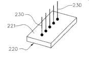
本发明的一具体实施例,揭示一种多部位探测的探针头模组。图2为该探针头模组的截面示意图,图3为该探针头模组的立体示意图,图4为该探针头模组的探针头基板的立体示意图。请参阅图2所示,该多部位探测的探针头模组200可装设在一多层印刷电路板310,以组成一探针卡。配合参阅图3,该探针头模组200主要包括一探针头基板210以及多数个探针转接片220,其中多数个探针230设置于该些探针转接片220,每一探针转接片220可对应于一待测集成电路,如一晶圆的其中一晶片或一卷带的其中一封装构造(图未绘出)。请参阅图4所示,该探针头基板210的一表面211定义有多数个矩阵排列的探测区212,每一探测区212内设有多数个连接垫213。该探针头基板210于该些探测区212之外可设置有多数个被动元件,以作电性保护与稳压。A specific embodiment of the present invention discloses a probe head module for multi-position detection. FIG. 2 is a schematic cross-sectional view of the probe head module, FIG. 3 is a perspective view of the probe head module, and FIG. 4 is a perspective view of the probe head substrate of the probe head module. Please refer to FIG. 2 , the
请参阅图5、图6A及图6B所示,该些探针转接片220具有一上表面221与一下表面222,该上表面221设有多数个探针230,该下表面222设有多数个接合端240。在本实施例中,该些接合端240可为焊球,能以回焊方式接合至该些连接垫213。该些探针转接片220可具有多数个贯孔223,以接合该些探针230的一固定端231。此外,每一探针230具有一悬空的探测端232,用以探触晶圆、BGA、TCP或TCP封装件等半导体产品的电极端或测试垫。较佳地,所有的探针转接片220可具有实质相同的尺寸、厚度与线路分布,具有通用性以利替换,故每一探针转接片220可互相共用与置换。Please refer to FIG. 5, FIG. 6A and FIG. 6B, the
请再参阅图2及图3所示,其中,每一探针转接片220接合至对应的探测区212,以使该些接合端240连接至该些连接垫213。在本实施例中,该些探针转接片220可具有与该探针头基板210相同的热膨胀系数。例如,该些探针转接片220可为半导体、陶瓷或胶片材质。Please refer to FIG. 2 and FIG. 3 again, wherein each
因此,在上述的多部位探测的探针头模组中,该些探针230不直接焊设于单一探针头,而是接合在个别的多数个探针转接片220,当部份的探针230发生故障或磨耗损伤时,仅需置换具有故障探针的探针转接片220而不需替换整个的探针头模组200(如图2及图3所示),具有节省成本、重工及增加使用方便性的功效。Therefore, in the above-mentioned probe head module for multi-position detection, these
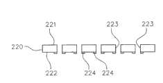
图7A至图7E进一步揭示前述探针转接片220设置探针230的制造方法。首先,请参阅图7A所示,提供多数个探针转接片220。每一探针转接片220具有一上表面221、一下表面222及多数个贯孔223,其中该下表面222设有多数个金属垫224,且该些金属垫224位于对应该些贯孔223的一端。在本实施例中,该些贯孔223贯穿该上表面221与该下表面222。FIG. 7A to FIG. 7E further disclose the manufacturing method of the
接着,请参阅图7B所示,置入多数个探针230于该些贯孔223中。每一探针230皆具有一固定端231与一探测端232,该些固定端231连接至一连接杆233并位于该些贯孔223内,该些探测端232具有突出于该探针转接片220的一致性高度。接着,请参阅图7C所示,填入一焊接剂250,用以焊接该些探针230的固定端231于该些贯孔223并使该些探针230与该些金属垫224达到电性连接。在本实施例中,该焊接剂250可为无铅焊料。在不同实施例中,该焊接剂250或可为导电胶。Next, as shown in FIG. 7B , a plurality of
之后,请参阅图7D所示,切断该连接杆233与该些探针230的连接。最后,请参阅图7E所示,设置多数个例如焊球的接合端240于该些探针转接片220的该下表面222,便可制成上述具有探针230的探针转接片220。After that, as shown in FIG. 7D , the connection between the connecting
以上所述,仅是本发明的较佳实施例而已,并非对本发明作任何形式上的限制,虽然本发明已以较佳实施例揭露如上,然而并非用以限定本发明,任何熟悉本专业的技术人员,在不脱离本发明技术方案范围内,当可利用上述揭示的技术内容作出些许更动或修饰为等同变化的等效实施例,但凡是未脱离本发明技术方案的内容,依据本发明的技术实质对以上实施例所作的任何简单修改、等同变化与修饰,均仍属于本发明技术方案的范围内。The above description is only a preferred embodiment of the present invention, and does not limit the present invention in any form. Although the present invention has been disclosed as above with preferred embodiments, it is not intended to limit the present invention. Anyone familiar with this field Those skilled in the art, without departing from the scope of the technical solution of the present invention, can use the technical content disclosed above to make some changes or modify equivalent embodiments with equivalent changes, but all the content that does not depart from the technical solution of the present invention, according to the present invention Any simple modifications, equivalent changes and modifications made to the above embodiments by the technical essence still belong to the scope of the technical solution of the present invention.
Claims (9)
Priority Applications (1)
| Application Number | Priority Date | Filing Date | Title |
|---|---|---|---|
| CNA200710079964XACN101256201A (en) | 2007-02-27 | 2007-02-27 | Probe head module for multi-part detection |
Applications Claiming Priority (1)
| Application Number | Priority Date | Filing Date | Title |
|---|---|---|---|
| CNA200710079964XACN101256201A (en) | 2007-02-27 | 2007-02-27 | Probe head module for multi-part detection |
Publications (1)
| Publication Number | Publication Date |
|---|---|
| CN101256201Atrue CN101256201A (en) | 2008-09-03 |
Family
ID=39891173
Family Applications (1)
| Application Number | Title | Priority Date | Filing Date |
|---|---|---|---|
| CNA200710079964XAPendingCN101256201A (en) | 2007-02-27 | 2007-02-27 | Probe head module for multi-part detection |
Country Status (1)
| Country | Link |
|---|---|
| CN (1) | CN101256201A (en) |
Cited By (10)
| Publication number | Priority date | Publication date | Assignee | Title |
|---|---|---|---|---|
| CN103869108A (en)* | 2014-03-17 | 2014-06-18 | 上海华虹宏力半导体制造有限公司 | Card clamping device and multiple-station testing device |
| CN103941049A (en)* | 2013-01-21 | 2014-07-23 | 华邦电子股份有限公司 | probe card |
| CN108254676A (en)* | 2018-03-26 | 2018-07-06 | 苏州联讯仪器有限公司 | A kind of high precision laser chip aging clamp |
| CN109253715A (en)* | 2017-07-13 | 2019-01-22 | 株式会社三丰 | Measuring Device Management System and computer-readable medium |
| CN109557444A (en)* | 2017-09-26 | 2019-04-02 | 颖崴科技股份有限公司 | Method for testing wafer-level electronic component |
| CN110940925A (en)* | 2019-12-28 | 2020-03-31 | 广东拓斯达科技股份有限公司 | Electricity core parameter detection machine |
| CN112305394A (en)* | 2020-11-06 | 2021-02-02 | 法特迪精密科技(苏州)有限公司 | Probe socket piece and probe assembly |
| CN116840526A (en)* | 2023-09-01 | 2023-10-03 | 江苏协和电子股份有限公司 | Needle head, PCB detection equipment using needle head and use method |
| CN117368545A (en)* | 2023-12-05 | 2024-01-09 | 苏州微飞半导体有限公司 | Plug-injection type conductive adhesive testing module |
| CN120594900A (en)* | 2025-08-07 | 2025-09-05 | 北京七星华创微电子有限责任公司 | Test seat for reducing contact resistance by mask plate method |
- 2007
- 2007-02-27CNCNA200710079964XApatent/CN101256201A/enactivePending
Cited By (13)
| Publication number | Priority date | Publication date | Assignee | Title |
|---|---|---|---|---|
| CN103941049A (en)* | 2013-01-21 | 2014-07-23 | 华邦电子股份有限公司 | probe card |
| CN103869108A (en)* | 2014-03-17 | 2014-06-18 | 上海华虹宏力半导体制造有限公司 | Card clamping device and multiple-station testing device |
| CN103869108B (en)* | 2014-03-17 | 2016-08-17 | 上海华虹宏力半导体制造有限公司 | Card holding device device and multi-functional position test device |
| CN109253715A (en)* | 2017-07-13 | 2019-01-22 | 株式会社三丰 | Measuring Device Management System and computer-readable medium |
| CN109557444A (en)* | 2017-09-26 | 2019-04-02 | 颖崴科技股份有限公司 | Method for testing wafer-level electronic component |
| CN108254676A (en)* | 2018-03-26 | 2018-07-06 | 苏州联讯仪器有限公司 | A kind of high precision laser chip aging clamp |
| CN110940925A (en)* | 2019-12-28 | 2020-03-31 | 广东拓斯达科技股份有限公司 | Electricity core parameter detection machine |
| CN112305394A (en)* | 2020-11-06 | 2021-02-02 | 法特迪精密科技(苏州)有限公司 | Probe socket piece and probe assembly |
| CN112305394B (en)* | 2020-11-06 | 2021-04-27 | 法特迪精密科技(苏州)有限公司 | Probe socket piece and probe assembly |
| CN116840526A (en)* | 2023-09-01 | 2023-10-03 | 江苏协和电子股份有限公司 | Needle head, PCB detection equipment using needle head and use method |
| CN116840526B (en)* | 2023-09-01 | 2023-10-31 | 江苏协和电子股份有限公司 | Needle head, PCB detection equipment using needle head and use method |
| CN117368545A (en)* | 2023-12-05 | 2024-01-09 | 苏州微飞半导体有限公司 | Plug-injection type conductive adhesive testing module |
| CN120594900A (en)* | 2025-08-07 | 2025-09-05 | 北京七星华创微电子有限责任公司 | Test seat for reducing contact resistance by mask plate method |
Similar Documents
| Publication | Publication Date | Title |
|---|---|---|
| CN101256201A (en) | Probe head module for multi-part detection | |
| KR101267145B1 (en) | Probe card | |
| JP2002005960A (en) | Probe card and its manufacturing method | |
| JP3741927B2 (en) | Semiconductor chip or package inspection apparatus and inspection method thereof | |
| US6727718B2 (en) | Electronic component package, printed circuit board, and method of inspecting the printed circuit board | |
| TW202035994A (en) | Contact terminal, inspection tool, and inspection device | |
| JP5535707B2 (en) | Display device and display device connection status inspection method | |
| JP2004053409A (en) | Probe card | |
| KR100681156B1 (en) | Socket for electrical test device | |
| JP2715793B2 (en) | Semiconductor device and manufacturing method thereof | |
| CN101146402A (en) | Circuit Pad Structure | |
| JP2002283049A (en) | Method of soldering contact pin, and contact pin | |
| JP2005183863A (en) | Method for manufacturing semiconductor integrated circuit device | |
| US7786478B2 (en) | Semiconductor integrated circuit having terminal for measuring bump connection resistance and semiconductor device provided with the same | |
| KR100632484B1 (en) | Vertical buffer probe card | |
| CN201069462Y (en) | Measuring device for circuit board | |
| CN110007117A (en) | Probe card | |
| TWI317427B (en) | Probe head module for multi-site probing | |
| JP2006005163A (en) | Semiconductor device, and mounting inspecting method thereof | |
| JP2006165325A (en) | Wiring structure of substrate mounted with IC package, and method of inspecting electrical connection failure | |
| KR20090079273A (en) | Probe card with pin-in-one space transformer | |
| JP2009158761A (en) | Wiring board for electronic component inspection device | |
| JP2021012040A (en) | Electrical property inspection jig | |
| JP4131137B2 (en) | Interposer substrate continuity inspection method | |
| TWI305273B (en) | A test assembly for testing a ball grid array package device |
Legal Events
| Date | Code | Title | Description |
|---|---|---|---|
| C06 | Publication | ||
| PB01 | Publication | ||
| C10 | Entry into substantive examination | ||
| SE01 | Entry into force of request for substantive examination | ||
| C02 | Deemed withdrawal of patent application after publication (patent law 2001) | ||
| WD01 | Invention patent application deemed withdrawn after publication | Open date:20080903 |