CN101252142A - Solid-state imaging device, manufacturing method thereof, and electronic device using same - Google Patents
Solid-state imaging device, manufacturing method thereof, and electronic device using sameDownload PDFInfo
- Publication number
- CN101252142A CN101252142ACNA2008100814292ACN200810081429ACN101252142ACN 101252142 ACN101252142 ACN 101252142ACN A2008100814292 ACNA2008100814292 ACN A2008100814292ACN 200810081429 ACN200810081429 ACN 200810081429ACN 101252142 ACN101252142 ACN 101252142A
- Authority
- CN
- China
- Prior art keywords
- solid
- state imaging
- resin
- film
- imaging element
- Prior art date
- Legal status (The legal status is an assumption and is not a legal conclusion. Google has not performed a legal analysis and makes no representation as to the accuracy of the status listed.)
- Pending
Links
Images


Classifications
- H—ELECTRICITY
- H10—SEMICONDUCTOR DEVICES; ELECTRIC SOLID-STATE DEVICES NOT OTHERWISE PROVIDED FOR
- H10F—INORGANIC SEMICONDUCTOR DEVICES SENSITIVE TO INFRARED RADIATION, LIGHT, ELECTROMAGNETIC RADIATION OF SHORTER WAVELENGTH OR CORPUSCULAR RADIATION
- H10F39/00—Integrated devices, or assemblies of multiple devices, comprising at least one element covered by group H10F30/00, e.g. radiation detectors comprising photodiode arrays
- H10F39/10—Integrated devices
- H10F39/12—Image sensors
- H—ELECTRICITY
- H10—SEMICONDUCTOR DEVICES; ELECTRIC SOLID-STATE DEVICES NOT OTHERWISE PROVIDED FOR
- H10F—INORGANIC SEMICONDUCTOR DEVICES SENSITIVE TO INFRARED RADIATION, LIGHT, ELECTROMAGNETIC RADIATION OF SHORTER WAVELENGTH OR CORPUSCULAR RADIATION
- H10F77/00—Constructional details of devices covered by this subclass
- H10F77/50—Encapsulations or containers
- G—PHYSICS
- G06—COMPUTING OR CALCULATING; COUNTING
- G06V—IMAGE OR VIDEO RECOGNITION OR UNDERSTANDING
- G06V10/00—Arrangements for image or video recognition or understanding
- G06V10/94—Hardware or software architectures specially adapted for image or video understanding
- G—PHYSICS
- G06—COMPUTING OR CALCULATING; COUNTING
- G06V—IMAGE OR VIDEO RECOGNITION OR UNDERSTANDING
- G06V40/00—Recognition of biometric, human-related or animal-related patterns in image or video data
- G06V40/10—Human or animal bodies, e.g. vehicle occupants or pedestrians; Body parts, e.g. hands
- G06V40/12—Fingerprints or palmprints
- G06V40/1335—Combining adjacent partial images (e.g. slices) to create a composite input or reference pattern; Tracking a sweeping finger movement
- H—ELECTRICITY
- H04—ELECTRIC COMMUNICATION TECHNIQUE
- H04N—PICTORIAL COMMUNICATION, e.g. TELEVISION
- H04N25/00—Circuitry of solid-state image sensors [SSIS]; Control thereof
- H—ELECTRICITY
- H10—SEMICONDUCTOR DEVICES; ELECTRIC SOLID-STATE DEVICES NOT OTHERWISE PROVIDED FOR
- H10F—INORGANIC SEMICONDUCTOR DEVICES SENSITIVE TO INFRARED RADIATION, LIGHT, ELECTROMAGNETIC RADIATION OF SHORTER WAVELENGTH OR CORPUSCULAR RADIATION
- H10F39/00—Integrated devices, or assemblies of multiple devices, comprising at least one element covered by group H10F30/00, e.g. radiation detectors comprising photodiode arrays
- H10F39/80—Constructional details of image sensors
- H10F39/804—Containers or encapsulations
- H—ELECTRICITY
- H01—ELECTRIC ELEMENTS
- H01L—SEMICONDUCTOR DEVICES NOT COVERED BY CLASS H10
- H01L2224/00—Indexing scheme for arrangements for connecting or disconnecting semiconductor or solid-state bodies and methods related thereto as covered by H01L24/00
- H01L2224/01—Means for bonding being attached to, or being formed on, the surface to be connected, e.g. chip-to-package, die-attach, "first-level" interconnects; Manufacturing methods related thereto
- H01L2224/42—Wire connectors; Manufacturing methods related thereto
- H01L2224/47—Structure, shape, material or disposition of the wire connectors after the connecting process
- H01L2224/48—Structure, shape, material or disposition of the wire connectors after the connecting process of an individual wire connector
- H01L2224/4805—Shape
- H01L2224/4809—Loop shape
- H01L2224/48091—Arched
- H—ELECTRICITY
- H01—ELECTRIC ELEMENTS
- H01L—SEMICONDUCTOR DEVICES NOT COVERED BY CLASS H10
- H01L2924/00—Indexing scheme for arrangements or methods for connecting or disconnecting semiconductor or solid-state bodies as covered by H01L24/00
- H01L2924/30—Technical effects
- H01L2924/301—Electrical effects
- H01L2924/3025—Electromagnetic shielding
Landscapes
- Engineering & Computer Science (AREA)
- Multimedia (AREA)
- Physics & Mathematics (AREA)
- General Physics & Mathematics (AREA)
- Theoretical Computer Science (AREA)
- Software Systems (AREA)
- Human Computer Interaction (AREA)
- Signal Processing (AREA)
- Solid State Image Pick-Up Elements (AREA)
- Image Input (AREA)
- Length Measuring Devices By Optical Means (AREA)
- Measurement Of The Respiration, Hearing Ability, Form, And Blood Characteristics Of Living Organisms (AREA)
Abstract
Translated fromChinese
Description
Translated fromChinese技术领域technical field
本发明涉及固态成像设备,并且更为具体地说,涉及诸如用于识别指纹的指纹传感器等用于检测物体的表面结构的接触式光学传感器所用的固态成像设备的结构及其制造方法。The present invention relates to a solid-state imaging device, and more particularly, to a structure of a solid-state imaging device for a contact optical sensor for detecting a surface structure of an object, such as a fingerprint sensor for recognizing a fingerprint, and a method of manufacturing the same.
背景技术Background technique
近年,对于根据生物模式来识别个体的需求日益增加。在生物模式中,指纹识别被定义为在历史上最古老的生物识别方法并且其结果被证明是有效的。近些年来,都已使用上了使用诸如玻璃环氧和陶瓷等刚性衬底的指纹输入设备。大量尺寸缩小和更加轻薄的指纹输入设备和光学传感器单元被公开。In recent years, there has been an increasing demand for identifying individuals based on biological patterns. Among biometrics, fingerprinting is defined as the oldest biometric method in history and its results are proven to be effective. In recent years, fingerprint input devices using rigid substrates such as glass epoxy and ceramics have been used. A large number of downsized and thinner fingerprint input devices and optical sensor units have been disclosed.
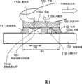
例如,JP 2005-18595 A(下面称之为专利文献1)公开了在散射光直接读取系统中使用固态成像元件(扫描传感器)的指纹输入设备。图1示出了它的典型例子。在图1中,标号130表示保护元件。专利文献1进一步公开了透明塑料片可以用作为保护元件的材料。进而,就提供低成本和提供微小图像来说,硅衬底是尤其优选的。而且,专利文献1公开了保护元件130被粘合到固态成像元件衬底101的固态成像元件101a。For example, JP 2005-18595 A (hereinafter referred to as Patent Document 1) discloses a fingerprint input device using a solid-state imaging element (scanning sensor) in a scattered light direct reading system. Figure 1 shows a typical example of it. In FIG. 1, reference numeral 130 denotes a protection element.
公开了其具体的粘合方法,其中当将保护元件130粘贴到固态成像元件衬底101时,粘合树脂(密封树脂)111被应用到固态成像元件衬低101的一侧上,并且之后保护元件130被粘贴于其,从而可以以防止渗出的粘合树脂111沿着保护元件130的上表面周围流动的方式将保护元件130进行粘合。A specific bonding method thereof is disclosed, in which when the protective element 130 is pasted to the solid-state
进而,专利文献1公开了在粘合树脂111中变得稀薄的区域可以从外围来进行补充,并且在这种情况下,粘合树脂111具有作为密封树脂的功能。Furthermore,
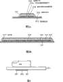
作为一种不使用专门的保护元件的方法,例如,如图2的典型例子所示,JP 03-142880 A(下面称之为专利文献2)公开了透明膜衬底211经由透明光固化绝缘树脂216安装有具有光接收元件214的半导体图像传感器芯片213。专利文献2进一步公开了使用紫外线经由透明膜衬底211对透明光固化绝缘树脂216进行照射并且因此使其硬化,从而完成了它的安装。As a method that does not use a dedicated protective element, for example, as shown in a typical example of FIG. 216 is mounted with a semiconductor
而且,专利文献2尽管未示出但是公开了图像传感器单元,也就是,包括被设备在透明膜衬底上的发光二极管的固态成像设备,其中由光接收元件所引导的光束的信息被通过半导体图像传感器芯片和输入/输出电路组件转换成图像输出信号,并且读取了位于透明膜衬底的上表面(与半导体图像传感器芯片等的安装表面相对)上的初始片。Also,
进而,JP 2004-173827 A(下面称之为专利文献3)公开了可以被缩小和变薄的光学传感器。光学成像元件340是经由位于未示出的制造衬底上的绝缘层来形成的,之后被从制造衬底上剥落,并且作为如图3所示的片形衬底被粘合到塑料片311。在这种情况下,在未示出的绝缘层上形成了光学成像元件。之后,将未示出的硬化型粘合剂施加到光学成像元件上,然后塑料片被粘合于其上,硬化型粘合剂硬化,并且光学成像元件340和塑料片311被固定。专利文献3公开了发光元件351也被通过粘合剂粘合到塑料片。Furthermore, JP 2004-173827 A (hereinafter referred to as Patent Document 3) discloses an optical sensor that can be downsized and thinned. The
如上所述,已经提出了大量有关小尺寸和薄固态成像设备以及图像传感器单元的建议。As described above, a large number of proposals on small-sized and thin solid-state imaging devices and image sensor units have been made.
考虑组装固态成像元件衬底,例如固态成像元件芯片,诸如覆盖其表面的膜等保护元件、膜形衬底和片形衬底等来总结那些现有技术,专利文献2和3公开了施加在固态成像元件衬底之间的粘合剂硬化。进而,专利文献1中的实施例的描述不包括词语“硬化”,不过,从粘合树脂(密封树脂)的描述中可以推断出在这种情况下粘合剂也是硬化的。Considering the assembling of solid-state imaging element substrates such as solid-state imaging element chips, protective members such as films covering their surfaces, film-shaped substrates and sheet-shaped substrates, etc. to summarize those prior arts,
不过,本发明的发明人遇到这种问题,即在设计固态成像设备,也就是诸如在根据现有技术的散射光直接读取系统中的指纹传感器等光学传感器单元的情况下,也就是说,通过使固态成像元件芯片和膜之间的树脂硬化,无法获取详细的图像,也就是,读取精确度下降。However, the inventors of the present invention encountered such a problem that in the case of designing a solid-state imaging device, that is, an optical sensor unit such as a fingerprint sensor in a scattered-light direct reading system according to the prior art, that is, , by hardening the resin between the solid-state imaging element chip and the film, a detailed image cannot be acquired, that is, the reading accuracy decreases.
作为进一步研究过程的结果,本发明的发明人发现低的读取精确度的原因来自,总结起来就是一点,即膜表面具有波纹,其导致进入到光接收元件部分的光束的不规则折射,并且因此妨碍了正常的识别。注意,后面将详细解释其机理。As a result of the further research process, the inventors of the present invention found that the cause of the low reading accuracy comes from, in summary, that the film surface has waviness, which causes irregular refraction of the light beam entering the light receiving element portion, and Normal recognition is thus prevented. Note that its mechanism will be explained in detail later.
发明内容Contents of the invention
本发明的目标主要是解决上述现有技术中固有的问题。也就是说,本发明提出了一种用于提高固态成像设备的读取准确度的技术方案,其中固态成像元件芯片位于膜上。The aim of the present invention is mainly to solve the problems inherent in the prior art mentioned above. That is, the present invention proposes a technical solution for improving the reading accuracy of a solid-state imaging device in which a solid-state imaging element chip is located on a film.
根据本发明的固态成像设备包括:安装于膜上的固态成像元件芯片;以及在膜和固态成像元件芯片之间具有流动性的树脂。A solid-state imaging device according to the present invention includes: a solid-state imaging element chip mounted on a film; and a resin having fluidity between the film and the solid-state imaging element chip.
具体地说,本发明的固态成像设备的特征在于提供在固态成像元件芯片和膜之间具有流动性的树脂。通过这个发明,经由作为被感知的物体的指纹等接收从发光体发射的光束,并且当通过膜接收到光束时,膜的接触表面在宏观结构上与诸如手指等物体相一致。因此,即使在膜上发生波纹,在膜和固态成像元件芯片之间具有提供的流动性的树脂避免了由波纹等所引起的不利影响,并且能够获得高可接受的视觉可识别性。这一事实是由本发明的发明人第一次发现的。下面将参考实施例描述中的附图来讲述其具体机理。Specifically, the solid-state imaging device of the present invention is characterized by providing a resin having fluidity between the solid-state imaging element chip and the film. With this invention, a light beam emitted from a luminous body is received via a fingerprint or the like as a sensed object, and when the light beam is received through the film, the contact surface of the film conforms macroscopically to an object such as a finger. Therefore, even if waviness occurs on the film, the resin having fluidity provided between the film and the solid-state imaging element chip avoids adverse effects caused by waviness or the like, and highly acceptable visual recognizability can be obtained. This fact was first discovered by the inventors of the present invention. The specific mechanism thereof will be described below with reference to the drawings in the description of the embodiments.
根据本发明的固态成像设备的制造方法包括的步骤有:将固态成像元件芯片安装在膜上;将光固化树脂放置在固态成像元件芯片和膜之间;并且在放置光固化树脂之后,通过使用光屏蔽元件来阻挡使光固化树脂硬化的光束,使光束的照射硬化正好位于固态成像元件芯片的光接收元件部分下面的区域之外的区域中的光固化树脂,而不硬化正好位于固态成像元件芯片的光接收元件部分下面的区域中的光固化树脂。也就是说,根据本发明的固态成像设备的制造方法通过设置树脂至少在正好在固态成像元件芯片的光接收元件部分下面的区域中具有流动性,而具有这种特征:防止由膜表面上的波纹所引起的不利影响,并且获得高度可接受的视觉可识别性。A method of manufacturing a solid-state imaging device according to the present invention includes the steps of: mounting a solid-state imaging element chip on a film; placing a photocurable resin between the solid-state imaging element chip and the film; and after placing the photocurable resin, by using A light shielding member to block a light beam that hardens the photocurable resin so that irradiation of the light beam hardens the photocurable resin in a region other than the region just below the light receiving element portion of the solid state imaging element chip without hardening just below the solid state imaging element Photocurable resin in the area under the light receiving element portion of the chip. That is to say, the manufacturing method of the solid-state imaging device according to the present invention has such a feature by providing the resin to have fluidity at least in a region just below the light-receiving element portion of the solid-state imaging element chip that prevents the Detrimental effects caused by moiré are eliminated and a highly acceptable visual recognizability is obtained.
进而,制造根据本发明的固态成像设备的方法是一种制造具有安装在膜上的固态成像元件芯片的固态成像设备的方法,该方法可以包括如下步骤:将固态成像元件芯片安装在膜上;将光固化树脂放置在固态成像元件芯片和膜之间;并且在放置光固化树脂之后,以使用固态成像元件芯片作为掩模的方式,使光束的照射硬化从固态成像元件芯片突出到外部的一部分光固化树脂。也就是说,根据本发明的固态成像设备的制造方法具有这种特性,即当形成具有流动性的树脂时,使用光固化树脂作为树脂,并且在由固态成像元件芯片利用固态成像元件芯片不发射光束的这一特性对光束进行屏蔽的区域中存在的树脂处于未被硬化的状态,也就是具有流动性的状态,从而防止由在膜表面上的波纹所产生的不利影响,并且使得能够获得高度可接受的视觉可识别性。Furthermore, the method of manufacturing a solid-state imaging device according to the present invention is a method of manufacturing a solid-state imaging device having a solid-state imaging element chip mounted on a film, and the method may include the steps of: mounting the solid-state imaging element chip on the film; placing a photocurable resin between the solid state imaging element chip and the film; and after placing the photocurable resin, in such a manner that the solid state imaging element chip is used as a mask, irradiation of a light beam hardens a part protruding from the solid state imaging element chip to the outside Light curing resin. That is to say, the manufacturing method of the solid-state imaging device according to the present invention has such characteristics that, when forming the resin having fluidity, a photocurable resin is used as the resin, and when the solid-state imaging element chip is used by the solid-state imaging element chip, no emission This characteristic of the beam shields the resin existing in the area where the beam is shielded in an unhardened state, that is, in a fluid state, thereby preventing adverse effects caused by ripples on the surface of the film and making it possible to obtain high Acceptable visual legibility.
根据本发明,获得了显示优良可识别性的固态成像设备。According to the present invention, a solid-state imaging device exhibiting excellent recognizability is obtained.
附图说明Description of drawings
在附图中:In the attached picture:
图1为截面图,示出了根据专利文献1的现有指纹输入设备;FIG. 1 is a cross-sectional view showing a conventional fingerprint input device according to
图2A和2B为截面图,示出了根据专利文献2的现有图像传感器;2A and 2B are sectional views showing a conventional image sensor according to
图3为截面图,示出了根据专利文献3的现有光学传感器;3 is a sectional view showing a conventional optical sensor according to
图4A和4B每一个示出了根据本发明的第一实施例的固态成像设备的整体;4A and 4B each show the whole of the solid-state imaging device according to the first embodiment of the present invention;
图5A和5B为截面图,每一个示出了根据本发明第一实施例的固态成像设备的主要部分;5A and 5B are sectional views each showing a main part of a solid-state imaging device according to a first embodiment of the present invention;
图6为图5B的S部分的放大的截面图;FIG. 6 is an enlarged cross-sectional view of part S of FIG. 5B;
图7为平面图,示出了根据第一实施例的固态成像设备的主要部分;7 is a plan view showing a main part of the solid-state imaging device according to the first embodiment;
图8A和8D是每一个示出了根据第一实施例的制造方法的视图;8A and 8D are views each showing a manufacturing method according to the first embodiment;
图9A和9B为结图形,每一个示出了第一实施例的效果;9A and 9B are knot diagrams, each showing the effect of the first embodiment;
图10为解释性视图,示出了在散射光直接读取系统中的指纹合成;FIG. 10 is an explanatory view showing fingerprint synthesis in a scattered light direct reading system;
图11A至11C为解释性视图,每一个更加详细地示出了第一实施例的效果;11A to 11C are explanatory views, each showing the effect of the first embodiment in more detail;
图12是示出了聚酰亚胺的透过特性的视图;FIG. 12 is a view showing transmission characteristics of polyimide;
图13A至13C是每一个示出了根据本发明的第二和第三实施例的固态成像设备的主要部分的视图;13A to 13C are views each showing a main part of solid-state imaging devices according to second and third embodiments of the present invention;
图14A至14C为制造过程视图,示出了本发明的第三实施例的特性;14A to 14C are manufacturing process views showing characteristics of a third embodiment of the present invention;
图15为结构性视图,示出了第三实施例的效果;Fig. 15 is a structural view showing the effect of the third embodiment;
图16为截面图,示出了本发明的第二或第三实施例的经过修订的例子;16 is a sectional view showing a revised example of the second or third embodiment of the present invention;
图17A和17B为透视图,示出了使用本发明第四实施例中的固态成像设备的移动电话;17A and 17B are perspective views showing a mobile phone using a solid-state imaging device in a fourth embodiment of the present invention;
图18为平面图,示出了第四实施例的固态成像设备;18 is a plan view showing a solid-state imaging device of a fourth embodiment;
图19是示出了第四实施例中的固态成像设备是如何被安装在便携式终端的弯曲部分上的视图;FIG. 19 is a view showing how the solid-state imaging device in the fourth embodiment is mounted on the curved portion of the portable terminal;
图20是示出了本发明的固态成像设备是如何被安装在小型电子设备上的视图;FIG. 20 is a view showing how the solid-state imaging device of the present invention is mounted on a small electronic device;
图21是示出了在本发明第五实施例中的固态成像设备的视图;以及FIG. 21 is a view showing a solid-state imaging device in a fifth embodiment of the present invention; and
图22为解释性视图,示出了工作中的第五实施例的设备。Fig. 22 is an explanatory view showing the apparatus of the fifth embodiment in operation.
具体实施方式Detailed ways
下面参考附图来讲述本发明的实施例。注意,贯穿所有附图,除非特别指出,共用组件使用相同的标号和数字来表示,并且适当地省略了对它们的解释。Embodiments of the present invention will be described below with reference to the drawings. Note that throughout all the drawings, unless otherwise specified, common components are denoted by the same reference numerals and numerals, and their explanations are appropriately omitted.
(第一实施例)(first embodiment)
下面参考图4A至图12来描述根据本发明第一实施例的固态成像设备。图4A和4B是示出了根据本发明第一实施例的固态成像设备10的整体的视图。图4A是示出了从组件安装表面侧所看的固态成像设备的平面图。图4B示出了从与组件安装表面相对的一侧所看的固态成像设备的平面图,其中该侧也就是由手指等所接触以识别指纹等的表面,也就是说,用于感应(检测)物体的固态成像设备表面,换句话说,其上放置了待检测的物体的表面或者由待检测的物体所接触的表面。注意,图4B示出了固态成像设备10,其处于将设备10沿着在图4A的线A-A’的方向上延伸的轴进行反转的状态,并且因此在其上下方向上反转安装组件5等,这将在后面进行讲述。进而,在图4B中省略了对衬底布线12、终端18等的解释。A solid-state imaging device according to a first embodiment of the present invention will be described below with reference to FIGS. 4A to 12 . 4A and 4B are views showing the whole of the solid-
参考图4A和4B,在固态成像设备10中,由例如聚酰亚胺形成的膜11的表面区域,其厚度在5微米至50微米的量级,安装有大量电子组件,诸如用于连接设备的衬底布线12、用于固态成像设备10的外部连接的端子18、每一个都被定义为发光体的类似发光二极管的发光元件5、以及以密封树脂7所保护的未示出的固态成像元件芯片1。这里,在后面的描述中,线A-A’和B-B’-B”表示截面方向,并且C表示诸如指纹等待感知的物体滑动的方向。需要注意的是,使得膜11的区域11a很宽,以便伸出端子18,不过,这个宽度的维度被均匀地设置,并且还可以被设置得与实际情况一样窄。进而,膜上的衬底布线12、外部连接引脚18等被未示出的绝缘保护材料所覆盖,其中排除用于安装组件和用于与其他元件进行连接所需要的区域。而且,膜11并不限于由聚酰亚胺等所形成的单层膜,而是可以具有层叠结构,在聚酰亚胺膜之间插入了粘合剂等。Referring to FIGS. 4A and 4B, in the solid-
注意,上面所述的大量电子组件被安装在膜11上,从而执行作为指纹传感器等的接触式光学传感器的功能,换句话说,可以被说成是传感器模块的功能。不过,这些功能并不直接与本发明有关,并且因此省却了对它们的讲述。进而,膜11具体由聚酰亚胺等来形成的,作为柔性印刷电路(下面缩写成FPC)的基本材料。注意到该基本材料的质量,换句话说,膜11的材料并不限于聚酰亚胺而可以是,如后面要讲述的,拦截例如硬化光固化树脂的紫外线等光束传输的柔性材料,并且透射诸如红外线和红色光束等从发光体发射出的光束。这些材料还可以被应用到其他有机膜。进而,膜11和衬底布线12可以被说成是FPC的组件的一部分。Note that a large number of electronic components described above are mounted on the
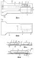
接下来,参考图5A至图7来描述本发明的第一实施例的主要部分。图5A和5B的每一个都是位于固态成像设备10的膜11的组件安装侧上的主要部分的放大的截面图,也就是沿着图4A的线A-A’和线B-B’-B”所取的放大的截面图。图5A为B-B’-B”部分的完整组件的截面图。图5B为A-A’部分的完整组件的截面图。图6为图5B的S部分的放大图。图7为透视平面图,示出了对应于图5A的B-B’的部分和图5B的部分,也就是,固态成像元件芯片1及其外围部件的视图。注意,图7是给定的视图,如后面所讲述的,用于解释具有流动性的树脂和外围固态树脂等之间的关系的目的,并且因此省略了图5A的衬底布线12等的解释。Next, the main part of the first embodiment of the present invention will be described with reference to FIGS. 5A to 7 . Each of FIGS. 5A and 5B is an enlarged cross-sectional view of a main part located on the component mounting side of the
贯穿这些附图,标号2b表示具有流动性的树脂,这应被视为本发明的最大意义之处。具体地说,树脂2b为例如紫外线硬化树脂等光固化树脂的未硬化部分。标号2a表示例如紫外线硬化树脂等固态树脂的硬化部分。进而,标号14表示不同于树脂2a的固态树脂。下面将解释其制造方法。而且,标号1表示固态成像元件芯片。注意,固态成像元件芯片在有些情况下被称为固态成像元件衬底,不过,该术语并不用于本说明书中。标号1a代表诸如互补金属氧化物半导体(CMOS)或电荷耦合器件(CCD)等固态成像元件,并且包括多种未示出的光接收元件。因此,固态成像元件1a也被称为固态成像元件芯片的固态成像元件部分,或者固态成像元件芯片的光接收元件部分。在下面的描述中,本说明书将针对固态成像元件1a或光接收元件部分1a,二者是相同意思。进而,固态成像元件芯片1的内部包括有存储器单元、控制单元等,尽管未示出,从而可以处理由固态成像元件1a所接收的图像信息。进而,固态成像元件芯片1被电气地连接到膜11的表面部分,换句话说,被经由设置于固态成像元件芯片1的光接收元件部分1a一侧上的突起3连接到在膜11上形成的衬底布线12。Throughout these drawings,
进一步参考图7,其中提供了在图6中示出的多个衬底布线12。所提供的对应于这些衬底布线的数目并且被电气地连接到衬底布线的多个未示出的突起3,执行的是输入/输出端子的角色,用于处理固态成像元件芯片1中的多种信息。进而,突起3的外围被固态树脂14所覆盖。注意,后面要讲到,在许多情况下固态树脂14在制造过程中是被作为树脂或膜来提供的,并且因此被称为树脂或膜14。需要指出的是,树脂或膜并没有被沿着突起电极的外围进行放置,这在后面要进行描述,其取决于安装突起3的方法,并且可以使用光固化树脂来作为替代物,这在第一实施例中未示出。Referring further to FIG. 7, a plurality of
如上所述,在第一实施例中,固态成像设备10包括具有在固态成像元件芯片1和膜11之间的流动性的树脂2b。而且,固态成像元件芯片的光接收元件部分1a在宏观上被认为由具有流动性的树脂2b所覆盖。进而,可以理解,具有流动性的树脂2b的外围被固态树脂2a和14所覆盖,以便不在固态成像元件芯片1和膜11之间进行流动。也就是说,固态树脂2a和14为密封树脂,用于密封具有流动性的树脂2b。因此可以说具有流动性的树脂的外围被密封树脂所覆盖。As described above, in the first embodiment, the solid-
而且,诸如发光二极管等发光元件5经由焊料15连接到膜11上的衬底布线12,以便使用红外线、近红外线、红光束等来照射诸如手指等目标物体。换句话说,发光体被安装于膜11的固态成像元件芯片1的安装表面侧上。可以通过后面要讲到的布线粘合来安装发光体,并且还可以在不同区域中提供,后面要进一步讲述,而不需要与固态成像设备进行集成。而且,固态成像元件芯片1被诸如环氧树脂等密封树脂7所保护。注意,如果固态树脂2a和14在密封流动树脂2b方面效果足够,则消除了对这种密封树脂7的需要。Also, a
进而,为给出一个不同的表达,将固态成像元件芯片1称为在FPC上进行倒装晶片安装的(下面被缩写为FC(倒装晶片))。这里,为了更进一步来讲述突起3,突起3包括例如金纽扣突起、镀金突起或焊料突起。将突起3进行FC连接到FPC的衬底布线12的方法涉及使用金-金压力焊接、金-金接触粘合、金-焊接、受控坍塌芯片连接(C4)技术,或者各向异性导电膜(下面缩写为ACF)连接。标号14表示用于稳定该连接、获得绝缘性和机械地保持固态成像元件芯片1的树脂或膜。Furthermore, to give a different expression, the solid-state
注意,在C4等技术的情况下,不放置树脂14和膜14不会引起任何不方便。更加详细地对其进行讲述,C4技术就是焊接突起,并且在有些情况下在没有树脂或膜的情况下来建立连接。在采用C4技术的情况下,会导致由于没有任何固态树脂而出现气缝。另外在这种情况下,如后面所讲述的,当填充诸如紫外线硬化树脂等具有流动性的树脂时,树脂还从该气缝溢流到外部而不是正好在固态成像元件芯片的下方。外部溢流的树脂硬化,并且因此不会出现内部树脂的任何溢流。Note that in the case of techniques such as C4, not placing the
进而,图5A、5B和图6为结构性放大截面图,其中根据位置不同而比例有很大不同。具体地说,优选情况下在固态成像元件芯片1和膜11之间的距离,换句话说,流动树脂部分的厚度,量级在5微米至50微米。更为优选的厚度是10微米至50微米的量级,这与膜11的厚度无关。而且,该厚度的上限根据用于识别指纹等的光的穿透性而受到限制,并且其下限根据后面要讲述的流动树脂的流动功能等而受到限制。另一方面,树脂上的固态成像元件芯片被认为是比树脂更厚。由于其他部分相同,因此省略了对它的解释。Furthermore, FIGS. 5A, 5B and 6 are structural enlarged cross-sectional views in which the scale is greatly different depending on the position. Specifically, it is preferable that the distance between the solid-state
为了说明图5A至图7的称为根据本发明的第一核心部分的结构,固态成像设备被构造成使得固态成像元件芯片1被FC安装于膜11上,并且诸如紫外线硬化树脂(下面将简记为紫外线(UV)硬化树脂)等的光固化树脂被填充到固态成像元件芯片1和膜11之间。固态成像设备也被称为是这样一种设备,其中只有着固态成像元件芯片1的外围光固化树脂沿暴露的表面区域才被硬化,而其余区域是未硬化区域,也就是具有流动性的树脂。为了更为详细地讲述,硬化部分,也就是固态树脂,也被称为是沿着矩形固态成像元件芯片的两个面对面的侧表面来形成的,更为确切地说,沿着图5A或图7的1X表面和面对1X的表面,以便覆盖住其外边缘。给另外一个表达,就是说对于固态成像元件芯片的1X表面来说,以与固态成像元件芯片的外边缘进行自对准的方式来提供密封元件。注意,现在使用了“以与固态成像元件芯片的外边缘进行自对准的方式来提供密封元件”的描述,不过,后面要继续讲述,如果设置的光束照射角度不是位于垂直方向上,而是位于倾斜方向上,则可以使位于固态成像元件芯片的外边缘附近的内部硬化。在这种情况下,也可以说以自对准的方式提供了密封元件。In order to explain the structure of FIGS. 5A to 7 called the first core part according to the present invention, the solid-state imaging device is constructed such that the solid-state
另外,进一步讲述第一实施例,还可以说固态成像设备被构造成使得固态成像元件芯片1被FC安装在其基本材料为聚酰亚胺的FPC上,具有流动性的树脂被填充在固态成像元件芯片1的固态成像元件1a和FPC之间。In addition, further describing the first embodiment, it can also be said that the solid-state imaging device is constructed such that the solid-state
下面参考图8A至8D来深入描述根据第一实施例的制造方法。图8A至8D是示出了制造对应于图5B的A-A’部分和图5A的B-B’部分的各部分的过程的视图。其解释意义存在于与安装固态成像元件芯片1的方式有关的部分中,并且因此将集中于这一点来进行讲述。The manufacturing method according to the first embodiment is described in depth below with reference to FIGS. 8A to 8D . 8A to 8D are views showing a process of manufacturing parts corresponding to the A-A' part of Fig. 5B and the B-B' part of Fig. 5A. Its explanatory significance exists in the section related to the manner in which the solid-state
首先,如图8A所示,固态成像元件芯片1经由突起3电气地连接到位于膜11的表面部分上的衬底布线12的预定部分上。此外,称为该操作用于建立经由突起3到FPC的衬底布线12的预定部分的电气连接。为了更加具体地描述一个例子,例如,每一个处于未硬化状态的树脂型膜和树脂位于衬底布线12上的连接目标部分中,相对膜和树脂的表面上推动突起3,并且然后以突起3伸出膜和树脂的方式,通过已知方法来建立连接。在这种情况下,如前面提到的,在膜11和固态成像元件芯片的固态成像元件1a之间的间隔优选情况下具有5微米至50微米的量级,并且更为优选情况下,以10微米至50微米的量级。First, as shown in FIG. 8A , the solid-state
之后,通过加热等来将树脂或膜11进行硬化。也就是说,树脂或膜11可以包括使用广义上被称为热固树胶的树脂。注意,在图8A的B-B’平面的视图中,固态成像元件芯片1初看是浮动的,不过,该视图示出了图4A的B-B’部分的截面图,并且为了确保光接收功能的目的,示出了该区域不包含任何保留于其上的组件,这对光接收来说是一个障碍。Thereafter, the resin or the
注意,如图7所示,优选情况下将树脂或膜沿着与固态成像元件芯片的B-B’部分相交的侧表面进行放置,也就是,放置得使其稍微从1X表面伸出来。从这一点来说,膜较容易被控制。进而,树脂或膜的材料可以涉及使用环氧树脂等。而且,膜11在组装阶段为模型的有机物质,并且在硬化之后可以被简单地称为固态树脂,换句话说。当倾注后面要讲到的紫外线硬化树脂时,固态树脂还起到密封元件的功能,并且可以称之为构建一部分密封元件。Note that, as shown in FIG. 7, it is preferable to place the resin or film along the side surface intersecting the B-B' portion of the solid-state imaging element chip, that is, so as to protrude slightly from the 1X surface. From this point of view, the membrane is easier to control. Furthermore, the material of the resin or film may involve the use of epoxy resin or the like. Also, the
之后,如图8B所示,在固态成像元件芯片1和膜11之间填充紫外线硬化树脂2。这一填充是由分配器等从例如固态成像元件芯片1的A-A’部分的侧表面在B-B’方向上进行的。结果,在该阶段处于未硬化状态下的树脂具有流动性,并且特别是在液态或半液态下。After that, as shown in FIG. 8B , an ultraviolet
需要指出的是,可以使用室温下粘度在0.1至10帕斯卡·秒(Pa·s)量级,也就是1至100泊松量级的紫外线硬化树脂来作为填充用的树脂。因此,换句话说,具有流动性的树脂可以是具有粘度的树脂。进而,它可以不特别地粘附到紫外线硬化树脂的材料上,不过,该树脂的基本材料可以包括使用像将丙烯酸根添加到环氧、聚酯、聚氨酯等主链的两个端子上的类型的材料,并且通过紫外线与丙烯酸根进行聚合而出现了反应根。注意,优选情况下环氧紫外线硬化树脂对固态成像元件没有不利影响,即使在未硬化状态下。It should be pointed out that an ultraviolet curable resin with a viscosity of 0.1 to 10 Pascal·s (Pa·s) at room temperature, that is, 1 to 100 Poisson, can be used as the resin for filling. Therefore, in other words, a resin having fluidity may be a resin having viscosity. Furthermore, it may not particularly adhere to the material of the UV curable resin, however, the base material of the resin may include the type using like adding acrylate groups to the two terminals of the main chain of epoxy, polyester, urethane, etc. material, and the reactive radicals appeared through the polymerization of ultraviolet rays and acrylate radicals. Note that it is preferable that the epoxy ultraviolet curable resin has no adverse effect on the solid-state imaging element even in an uncured state.
而且,当使用紫外线硬化树脂进行填充时,根据其粘度,如图7的平面图所示,紫外线硬化树脂可以在树脂或膜11的外部周围进行流动,不过,该环绕流动并不是必不可少的。简而言之,外部树脂2a覆盖1X表面的两侧,其程度足以使具有流动性的内部树脂无法流出。Also, when filled with an ultraviolet curable resin, depending on its viscosity, the ultraviolet curable resin may flow around the outside of the resin or
进而,当填充紫外线硬化树脂时,在图8B中,如沿着B-B’方向的视图所示,优选情况下倾注树脂的量应当使其在固态成像元件芯片1的B-B’方向上伸出外侧。注意,如前面讲述的,当执行图8A的过程时,通常树脂或膜11沿着该方向,也就是阶进方向上的侧表面逐渐硬化,并且该树脂在图8B的A-A’方向上并不流出。进而,因此可以容易地计算和控制填充的树脂量。注意,尽管在第一实施例中未示出,如果不像在C4技术中那样使用树脂14,则优选情况下使用这个量来倾注树脂,以便从图5B的1Y表面伸出去。注意,“优选情况下倾注树脂的量应当使其在固态成像元件芯片1的B-B’方向上伸出外侧”的描述具有这种意思,就是后面要讲到的,通过使用倾斜向上的光束来照射树脂,可以使紫外线硬化树脂稍微硬化到从其外部边缘的附近深入固态成像元件芯片1的内部。因此,当在平面方向上来看紫外线硬化树脂时,使紫外线硬化树脂伸出到固态成像元件芯片1的外部并不是必不可少的。Furthermore, when the ultraviolet curable resin is filled, in FIG. 8B, as shown in the view along the BB' direction, it is preferable to pour the resin in such an amount that it is in the BB' direction of the solid-state
接下来,如图8C所示,基本上在从上垂直向下的方向上使用紫外线(UV)来照射固态成像元件芯片1。可以对应于待使用的树脂来设置照射强度,也就是,可以以由树脂制造商所推荐的水平来设置。进而,设置关于照射时间周期是相同的。在一个例子中,可以以一秒或更长时间为量级来设置照射时间,这不会在制造方面成为约束。从而,使固态成像元件芯片1的外围部分2a的区域中的树脂硬化。另一方面,包括了位于固态成像元件1a的正下方部分的正好位于固态成像元件芯片1下面的部分上的树脂2b,在其中紫外线的照射被固态成像元件芯片1所遮挡,而保持不硬化的状态。也就是说,树脂保持在初始液态或半液态下,并且具有流动性。因此,在该区域中的树脂2b被称之为基本上与树脂2相同。因此,通过附图中标号的标注,可以将树脂2b表示为树脂2,不过,与硬化部分2a相比,该树脂被表示成树脂2b。该制造方法保证了外围树脂的硬化,并且因此未硬化的树脂不流出。注意,在采用未示出的C4技术的情况下,如上所述,从1Y表面伸出的树脂硬化,并且没有树脂的流出。如上面所解释的,硬化部分扮演着未硬化树脂的密封元件的角色。进而,像在C4技术中那样,如果焊料等被曝光,则焊料等可以称之为构成密封元件的一部分。因此,密封元件并不限于树脂,防止具有流动性的树脂流出的任何元件都是可以的。Next, as shown in FIG. 8C , the solid-state
而且,下面使用紫外线硬化树脂作为光固化树脂的一个例子进行了讲述。不过,在不使用由紫外线硬化的光固化树脂的情况下,光固化树脂可以是在其中光束被固态成像元件芯片所遮挡而在芯片下面没有硬化,并且在其中光束被片(膜)11所遮挡的树脂,这是光束在使用中的特性。进而,讲述了这种制造方法,即在膜11上安装固态成像元件芯片1之后,倾注并且在其间填充光固化树脂。不过,在不遵守该方法的情况下,例如,尽管未示出,在已经将光固化树脂放置在膜11的预定部分中之后,安装固态成像元件芯片1,也就是说,经由突起3将其连接到衬底布线12。进而,上面作了“基本上在从上垂直向下的方向上使用诸如紫外线等光束来照射固态成像元件芯片1”的描述,不过,照射光束可以以倾斜向上方向照射。在这种情况下,位于固态成像元件芯片1的外围部分中的光固化树脂可以硬化,并且位于外部部分中的树脂可以减少并且在最小情况下可以进一步减少到“0”,从而获得能够使设备尺寸缩小的效果。Also, the following describes using an ultraviolet curable resin as an example of a photocurable resin. However, in the case of not using a photocurable resin hardened by ultraviolet rays, the photocurable resin may be one in which the light beam is blocked by the solid-state imaging element chip without hardening under the chip, and one in which the light beam is blocked by the sheet (film) 11 The resin, which is the characteristic of the beam in use. Furthermore, a manufacturing method is described in which, after mounting the solid-state
之后,如图8D所示,整个部分被诸如环氧树脂等密封树脂7所密封。注意,诸如发光元件5等其它电子组件可以在之后进行安装,并且还可以以与安装固态成像元件芯片1的过程相同的过程来进行安装。进而,这些电子组件可以在该过程之前进行安装,也就是,在图8A的过程之前。通过上面所述的操作,就完成了固态成像设备10。注意,前面已经讲到,可以不使用密封树脂7。After that, as shown in FIG. 8D, the entire portion is sealed with a sealing
而且,在不使用紫外线硬化树脂而是使用由表现出高得多的渗透性的光束来硬化的树脂的情况下,以及在固态成像元件芯片变得薄到足够透射紫外线的情况下,在如图8C所示的过程中,未示出的屏蔽特别地位于固态成像元件芯片中的固态成像元件1a的上部或朝上的部分中,从而至少使正好位于固态成像元件1a下方的部分中的树脂不硬化,而其他部分中的树脂可以硬化。正如后面要讲到的,这种情况还获得了提高可识别性的效果。注意,在这种情况下,尽管可能产生具有流动性的内部树脂在实际使用的状态下通过紫外线等硬化并且变得无法执行其功能的怀疑,正如后面要讲到的,通常情况下固态成像设备被安装在移动电话、便携式终端、电子设备等的每一个的外壳的内部中。因此,诸如紫外线等光束被外壳的薄金属部分等所遮挡,并且因此不会产生使用等问题。Also, in the case of not using an ultraviolet curable resin but a resin cured by a light beam exhibiting much higher permeability, and in the case where the solid-state imaging element chip becomes thin enough to transmit ultraviolet rays, in the case of In the process shown in 8C, an unillustrated shield is located particularly in the upper or upward portion of the solid-
下面参考附图来讲述第一实施例的效果。图9A示出了如何通过使用根据本发明的固态成像设备10来识别指纹的视图。图9B为图9A的A部分的放大视图。识别指纹,也就是,以如图9A所示来自类似发光元件5的发光体的光束穿透指纹内部的方式感知指纹,并且经由指纹内部进行传输和离开指纹区的光束被感知到。也就是说,在从外部撞击到手指上的光束中,穿过手指的内部前进并且离开指纹区的光束被检测到。下面将讲述其细节。The effect of the first embodiment will be described below with reference to the drawings. FIG. 9A is a view showing how to recognize a fingerprint by using the solid-
根据本发明的第一实施例,如图9B所示,具有流动性的树脂是位于手指在其上滑动以识别指纹的由手指所接触的部分上的固态成像元件(光接收元件部分)1a和膜11之间的树脂2b,换句话说,树脂2b位于FPC和光接收部分1a之间。因此,可以防止由FPC的膜11的表面的波纹所导致的指纹识别准确度的下降。位于光接收元件部分1a和膜11之间的树脂2b的厚度可以是,如早先所述的5微米至50微米的量级,并且更为优选情况下,为10微米至50微米。进而,有关“树脂2b具有流动性,并且因此可以防止由FPC的膜11的表面的波纹所导致的指纹识别准确度的下降”的描述换句话说可以表示“树脂2b处于液态或半液态,或者具有粘度,并且因此可以防止由FPC的膜11的表面的波纹所导致的指纹识别准确度的下降”。注意,树脂2b的粘度没有被限定于0.1至10帕斯卡·秒(Pa·s)但是可以被设置到在使用的状态下具有流动性的程度。下面将更加详细地来讲述这一点。According to the first embodiment of the present invention, as shown in FIG. 9B , the resin having fluidity is the solid-state imaging element (light receiving element portion) 1a located on the portion touched by the finger on which the finger slides to recognize the fingerprint and The
图10为解释性视图,示出了当在散射光直接读取系统中使用固态成像元件(扫描传感器)来识别指纹时的解释性视图。指纹在图10的C方向上滑动。这里,图10的C方向与图4B的C方向相同。在图10的中心区域中示出了时间流。各碎片的带状指纹图像的重叠部分被重构以形成指纹图像。这是使用扫描传感器的固态成像设备的基本原则。FIG. 10 is an explanatory view showing when a fingerprint is recognized using a solid-state imaging element (scanning sensor) in a scattered light direct reading system. The fingerprint slides in the direction C of FIG. 10 . Here, the C direction in FIG. 10 is the same as the C direction in FIG. 4B . The time flow is shown in the central area of FIG. 10 . Overlapping portions of the striped fingerprint images of the shards are reconstructed to form a fingerprint image. This is the basic principle of solid-state imaging devices using scanning sensors.
这里,将参考图11A、11B和11C来讲述膜表面的状态和树脂之间的关系和光学关系。也就是说,下面将更加详细地讲述本发明的第一实施例的效果。图11A和11B示出了基于现有技术的例子。具体地说,这是其中膜具有波纹的情况,并且在膜和固态成像元件(光接收元件部分)之间存在硬化树脂。Here, the relationship and optical relationship between the state of the film surface and the resin will be described with reference to FIGS. 11A , 11B, and 11C. That is, the effect of the first embodiment of the present invention will be described in more detail below. 11A and 11B show examples based on the prior art. Specifically, this is a case where the film has waviness, and there is a hardened resin between the film and the solid-state imaging element (light-receiving element portion).
如图11A所示,当入射到手指内部的光束穿过指纹区域中时,指纹的突出区域直接接触该膜,其结果是穿透的光束直接进入光接收元件部分1a,而指纹的凹进区域不接触该膜,其结果是光束不到达固态成像元件。穿过并且从指纹的突出区域向后传播的光束的信息条被收集和识别,如图10所示,也就是,被重新合成到指纹信息中。进而,图11A示意性地示出了由指纹的突出区域所接触的膜区域在局部比较起来是扁平的,而没有波纹,并且因此光束直接到达固态成像元件。As shown in FIG. 11A, when a light beam incident on the inside of the finger passes through the fingerprint area, the protruding area of the fingerprint directly contacts the film, with the result that the penetrating light beam directly enters the light
不过,根据现有技术,当手指滑动并且达到如图13所示的状态时,也就是,指纹的突出区域接触膜的波纹区域时,光束在如图11B所示的波纹区域中被折射。也就是说,总结如图11A和11B所示的状态,得出结论是光束被不规则地折射。因此,难以搜索到重叠的部分,并且难以进行指纹的重新合成。也就是说,无法获得详细的指纹图像。注意,尽管未示出,本发明人验证了在检查的过程中不提供膜而仅设置硬化树脂的情况下的指纹读取准确度。不过,在这种情况下无法获得良好的视觉可识别性。作为观察用于验证的树脂的结果,证实了树脂表面不是光滑的而是粗糙的。考虑到了这种情况还经历了光束的不规则折射。However, according to the prior art, when the finger slides and reaches the state shown in FIG. 13 , that is, when the protruding area of the fingerprint contacts the corrugated area of the film, the light beam is refracted in the corrugated area as shown in FIG. 11B . That is, summarizing the states shown in FIGS. 11A and 11B , it is concluded that the light beam is irregularly refracted. Therefore, it is difficult to search for overlapping parts, and it is difficult to resynthesize fingerprints. That is, detailed fingerprint images cannot be obtained. Note that, although not shown, the present inventors verified the fingerprint reading accuracy in the case where no film was provided but only hardened resin was provided during inspection. However, good visual recognizability cannot be obtained in this case. As a result of observing the resin used for verification, it was confirmed that the surface of the resin was not smooth but rough. Taking this into account also experiences irregular refraction of the light beam.
另一方面,图11C为示意性视图,示出了本发明第一实施例的情况,也就是其中树脂2b具有流动性的情况。膜11自身具有波纹,不过,即使膜11是波纹的,其下的树脂2b具有流动性。因此,通过指压的凹痕,波纹沿着手指皮肤减少,或者转移到固态成像元件(光接收元件部分)1a的光接收区域的外部,因此考虑到可以通过促进指纹图像的重新合成来获得详细指纹图像,而在折射中没有任何变化出现。目前所讲述的是本发明的发明人的第一发现。On the other hand, FIG. 11C is a schematic view showing the case of the first embodiment of the present invention, that is, the case in which the
注意,本发明的发明人的研究结果表明,当在FPC上FC安装固态成像元件芯片1等时最容易出现膜11的表面波纹。更加详细地来说,需要在固态成像元件芯片(下面简称之为芯片1)的突起和FPC的衬底布线12之间获得金属连结,且因此当直接加热芯片1和FPC时发生波纹。进而,当将电子组件等放置到FPC上的衬底布线12时所进行的焊接是成为产生波纹的因素的过程。因此,那些过程对于获得薄而灵活的产品来说是必不可少的,并且因此难以避免波纹。而且,换句话说,还可以说是波纹是在当加热有机膜时产生的,并且因此,即使膜没有像FPC那样构造,也就是说,像专利文献1中所公开的那样,可以推测在只根据有机膜来简单地大范围集成保护元件的情况下出现波纹。作为即使在波纹存在时的详细图像获取方法,本发明的发明人提出了一种将具有流动性的树脂2b放置在固态成像元件芯片的光接收元件部分1a和膜11之间的方法。因此,足以使具有流动性的树脂至少存在于正好位于光接收元件部分1a下面的区域中。Note that the inventors of the present invention have found that surface waviness of the
进而,拿聚酰亚胺来作为使用第一实施例的膜11的例子,也就是作为FPC的基本材料的例子,不过,聚酰亚胺遮挡紫外线(在图12中由380nm以下的波长来表示)但是透射红外线。因此,使用聚酰亚胺来作为第一实施例的膜,从而从自然世界发射的紫外线在被制造后在使用状态中被遮挡,不进行UV硬化树脂的任何硬化过程,并且对具有流动性的状态,也就是待保持的液体/半液体/粘稠状态具有长期保持效果。Furthermore, take polyimide as an example of using the
(第二实施例)(second embodiment)
接下来,参考图13A至13C来讲述本发明第二实施例,特别是将重点放在与第一实施例中不相同的那些部分。下面对第二实施例中的固态成像设备30进行简短解释,固态成像设备30的特征在于向第一实施例添加(形成)光屏蔽布线13。优选情况下,以如图13C所示的框架形状来形成光屏蔽布线13。下面是稍微详细的讲述。Next, a second embodiment of the present invention will be described with reference to FIGS. 13A to 13C, particularly focusing on those parts that are different from those in the first embodiment. The following briefly explains the solid-
图13A为对应于第一实施例中的图5A的视图。与第一实施例的不同之处在于光屏蔽布线13是沿着外围提供的,与光接收元件部分1a的正下方表面有间隔,该表面与膜11上具有流动性的树脂2b相接。这与图13B的光屏蔽布线13是相同的。图13C示出了与图7的部分相对应的部分的放大平面图(示意性截面图)。光屏蔽布线13以框架形状包围着光接收元件部分1a的外围。该结构除了遮挡来自发光元件5的经由手指入射到固态成像元件1a上的光束以外,还遮挡外部多余的光。也就是说,由于来自手指的散射光的比例增加,可以提高指纹图像的电子信号的S/N(信号与噪声)比率,并且可以获取更为优选的图像,这是在第一实施例中所没有获得的特定效果。Fig. 13A is a view corresponding to Fig. 5A in the first embodiment. The difference from the first embodiment is that the light-shielding
注意,光屏蔽布线尽管被描述为用于进行光屏蔽的布线,但是可以由同样的材料来形成,并且与通常的电子连接所使用的衬底布线12的材料具有相同的厚度。进而,根据需要可以改变其厚度。进而,也可以替换其他材料。注意,该制造方法基本上与第一实施例中的相同,不同点在于是否制备了包括设置于膜11上的光屏蔽布线13的元件,并且因此省略了对该制造方法的详细解释。Note that the light-shielding wiring, although described as wiring for light-shielding, may be formed of the same material and have the same thickness as that of the
而且,尽管已经作了关于“优选情况下以框架形状来形成光屏蔽布线”的讲述,不过,该形状并不一定是框架形状的,并且实际上,中途还可以形成间断。对于其他人来说,实际上可以以诸如局部变薄的形状等多种形式来修改该形状。Also, although a remark has been made about "preferably forming the light-shielding wiring in a frame shape", the shape does not necessarily have to be a frame shape, and actually, a discontinuity may be formed halfway. For others, the shape can actually be modified in a variety of ways, such as locally thinned shapes.
(第三实施例)(third embodiment)
除了参考图13A至13C以外,下面将参考图14A至15来讲述本发明的第三实施例。简而言之,第三实施例中的固态成像设备40的特征是,将第二实施例中的光屏蔽布线13连接到接地端子等,从而具有静电故障预防作用。A third embodiment of the present invention will be described below with reference to FIGS. 14A to 15 in addition to FIGS. 13A to 13C. In short, the solid-state imaging device 40 in the third embodiment is characterized in that the light-shielding
第三实施例中沿着线A-A’的截面图和沿着线B-B’-B”的截面图与图13A和13B相同。不同点在于,那些截面图是平面图。图14A、14B和14C示出了位于制造过程中间的部分,以便清楚地给出不同点。图14A和14B为安装固态成像元件芯片1之前膜11等的截面图。图14A和14B与第二实施例中的附图相同,尽管在第二实施例的讨论中没有示出。不同点在于,如图14C的平面图所示,光屏蔽布线13经由膜11上的衬底布线12连接到端子18上。注意,端子18被连接到未示出的外部设备的端子和外部设备的导电部分等,并且接地。The sectional view along the line AA' and the sectional view along the line BB'-B" in the third embodiment are the same as FIGS. 13A and 13B. The difference is that those sectional views are plan views. FIGS. 14A, 14B 14C and 14C have shown the part that is positioned at the middle of manufacturing process, so that clearly give different point.Fig. 14A and 14B are the sectional views of
下面将参考图15来讲述根据本发明第三实施例的固态成像设备40的效果。根据第三实施例,由于包括也用作接地布线13的光屏蔽布线13,除了提高在第二实施例中所讲述的指纹图像的电子信号的S/N比率以外,还可以获得特别的效果,即通过为在诸如手指等人体中所积累的静电构建放电路径,从而不会对固态成像元件芯片1以及它的光接收元件部分1a施加因静电而引起的不利影响。The effect of the solid-state imaging device 40 according to the third embodiment of the present invention will be described below with reference to FIG. 15 . According to the third embodiment, since the light-shielding
(第一、第二和第三实施例的修正例子)(Modified examples of the first, second and third embodiments)
上述的实施例已经作为焊接到膜11的衬底布线12上的发光元件5的例证。也就是说,在FPC上对发光元件5进行表面安装的例子已经有例证,不过,可以通过引线粘合来安装该发光元件5。图16示出了固态成像设备50的例子,其中在第二和第三实施例中发光元件5通过涉及使用粘合引线19的引线粘合来进行安装。通过引线粘合来进行安装还具有与通过安装离散的发光元件,也就是封装的发光元件相比能够进一步缩小尺寸的效果。注意,图16的标号27表示引线粘合连接部分的保护树脂。进而,在这种情况下,发光元件5经常整体地连接到衬底布线12,并且因此,尽管考虑光束是否可以到达诸如手指等目标物体,但是由于具有由保护树脂27所反射的光束并且进入手指,因此实际使用中不存在问题。The above-described embodiments have been exemplified as the
(第四实施例)(fourth embodiment)
接下来,参考附图17A至19来讲述将固态成像设备安装到诸如移动电话等便携式终端也就是便携式电子设备上的实施例。图17A和17B示出了将如上所述的根据本发明的固态成像设备安装到移动电话70上的例子。至于安装部分,固态成像设备实际上可以被安装到包括有按钮73、点击部分74等的主屏部分上,不过,这种方案在本发明的灵活性方面没有提供显著的效果。Next, an embodiment in which a solid-state imaging device is mounted on a portable terminal such as a mobile phone, that is, a portable electronic device will be described with reference to FIGS. 17A to 19 . 17A and 17B show an example of mounting the solid-state imaging device according to the present invention as described above on a
情况是这样,对于安装部分来说,下面要讲述将固态成像设备安装于弯曲部分,即,由移动电话70的70A所表示的部分上的例子。注意,实际上安装部分可以包括侧表面部分70B、70C、70D等。This being the case, as for the mounting portion, an example of mounting the solid-state imaging device on the curved portion, ie, the portion indicated by 70A of the
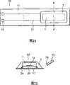
图18为平面图,示出了本发明的固态成像设备60。图18示出了诸如发光元件5、固态成像元件芯片1、密封树脂7和电容器51等电子组件的元件。注意,省略了对膜上的布线和端子的解释,不过,端子部分位于膜50的宽度-窄度方向上。图18示出了其中端子部分的宽度较小的例子,这与图4A和4B不同。注意,实际上,诸如使用具有流动性的树脂等本发明的特征方案涉及从第一至第三个实施例的任何一个,或者其修正例子的任何一个,并且因此省略了对其制造方法等的详细讲述。FIG. 18 is a plan view showing a solid-
图19为截面图,示出了将本发明的固态成像设备60安装到移动电话的弯曲部分70A上。根据本发明,如图19所示,可以将固态成像设备60有效地安装在移动电话的电话群71的弯曲部分70A上。下面通过给出更为具体的数字来描述一个例子,例如,如果电话外壳的厚度T的尺寸被设置为大约1mm,该厚度是达到根据本发明实施例的固态成像设备基本上被设置为如附图所示样子的程度。进而,对于用于安装每个用作指纹传感器部分的固态成像元件1和流动性树脂2b的尺寸,也就是,对于图5A和13A的B-B’部分的尺寸,大约3-4mm的扁平部分足以用作由手指所接触的指纹传感器。在这种情况下,如图19中的尺寸L所示,在半弯部分中可以设置发光元件5等。实际上,固态成像设备的结构可以在图18、4A和4B的结构以及其他结构内部来任意确定,这取决于其装配部分。FIG. 19 is a cross-sectional view showing mounting of the solid-
如上所述,根据本发明,固态成像设备可以被有效地安装在诸如移动电话等移动终端和移动电子设备的侧表面和弯曲部分上,从而有助于缩小整个的便携式电子设备。为了更好地理解它,也可以说本发明有助于缩小电子设备的尺寸。As described above, according to the present invention, a solid-state imaging device can be efficiently mounted on side surfaces and curved portions of mobile terminals such as mobile phones and mobile electronic devices, thereby contributing to downsizing of the entire portable electronic device. To understand it better, it can also be said that the invention helps to reduce the size of electronic devices.
(第四实施例的修正例子)(A modified example of the fourth embodiment)
注意,图20示出了将固态成像设备安装在诸如手持式小型个人计算机和便携式游戏机等小型电子设备80的侧表面上的一个例子,并且还示出了第四实施例的经过修正的例子。实际上,本发明的固态成像设备可以被安装在包括显示部分81、操作按钮82等的表面80B上,不过,如果该表面的空间不够,则固态成像设备可以被安装在侧表面80A等上。注意,在这种情况下的方法与第四实施例中的一样,并且因此省略了对它的详细解释。电子设备比前面讲述的移动电话的外壳要厚得多,因此手指可以容易地触摸侧表面,从而取得促进指纹识别的效果。Note that FIG. 20 shows an example of mounting the solid-state imaging device on the side surface of a small
(第五实施例)(fifth embodiment)
图21和22示出了根据本发明第五实施例的固态成像设备,其中发光元件没有位于膜11上。也就是说,在根据本发明的固态成像设备中,待安装到膜上的发光元件不是必不可少的。图21示出了根据本发明的固态成像设备90,它包括固态成像元件芯片1、密封树脂7、衬底布线12和端子18。注意,在图21中省略了对电子组件等的解释。21 and 22 show a solid-state imaging device according to a fifth embodiment of the present invention in which the light emitting element is not located on the
图22为图21的E-E’部分的放大截面图。与图5A不同之处在于,除了没有发光元件以外,其尖端具有光散射部分76等的光纤75被包括在未示出的手持外壳中,并且因此位于固态成像设备90的侧表面上,例如,像在第一实施例等中的那样,位于临近具有发光元件5的区域的位置处,从而从其提供光束。这是一个能够使指纹被识别的例子。该方法对于像移动电话和便携式终端等具有固态成像设备的设备在逐渐缩小尺寸并且缺少放置发光元件的空间等情况是有用的。Fig. 22 is an enlarged sectional view of part E-E' of Fig. 21 . The difference from FIG. 5A is that, except that there is no light emitting element, the
注意,关于本发明实施例的讨论集中在使用用于读取指纹的固态成像设备的例子。对在移动电话和小型电子设备上安装固态成像设备的例子进行进一步讨论。不过,根据本发明的固态成像设备的应用范围并不限于对指纹的读取。例如,固态成像设备对于作为光学传感器设备通过使用来自外部的光束在表面上照射具有粗糙结构(突出和凹进的区域)的目标物体来检测表面状态来说是非常有用的,例如在人体和其他活体生物的脸部和皮肤上,然后通过接触让光束穿过其内部并且检测从突出的区域传播回来的光束。而且,该应用不限于这一方案,而是可以广泛地延伸,将其作为光学传感器设备,通过让目标物体接触膜11或将目标物体放置在膜11上来检测表面上具有粗糙度的目标物体的形状,并且使用来自外部的光束照射目标物。Note that the discussion about the embodiments of the present invention focuses on the example of using a solid-state imaging device for reading fingerprints. Examples of solid-state imaging devices mounted on mobile phones and small electronic devices are discussed further. However, the application range of the solid-state imaging device according to the present invention is not limited to the reading of fingerprints. For example, solid-state imaging devices are useful as optical sensor devices to detect surface states by illuminating target objects with rough structures (protruded and recessed areas) on the surface using a beam of light from the outside, such as in the human body and other On the face and skin of living organisms, the beam is then passed through by contact and the beam traveling back from the protruding area is detected. Also, the application is not limited to this solution, but can be broadly extended as an optical sensor device to detect a target object having roughness on its surface by letting the target object touch the
进而,针对本发明的讨论已经集中于使用扫描传感器的固态成像设备。不过,从进一步改进不是使用扫描传感器而是使用二维传感器的固态成像设备中的视觉可识别性的观点来看,可认为像在本发明中那样提供具有流动性的树脂是有用的。因此,本发明的可应用范围并不限于使用扫描传感器的固态成像设备。目前来讲,已经参考附图对于本发明进行了合适的讨论,不过,本发明实际上可以在不固守上述所公开的内容的情况下被合适地修正和更改,只要在本发明的主旨范围内。Furthermore, discussion of the present invention has focused on solid-state imaging devices using scanning sensors. However, from the viewpoint of further improving visual recognizability in a solid-state imaging device using not a scanning sensor but a two-dimensional sensor, it is considered useful to provide a resin having fluidity as in the present invention. Therefore, the applicable range of the present invention is not limited to a solid-state imaging device using a scanning sensor. So far, the present invention has been properly discussed with reference to the accompanying drawings, however, the present invention can actually be properly modified and changed without sticking to the above-disclosed content, as long as it is within the scope of the present invention .
Claims (17)
Translated fromChineseApplications Claiming Priority (2)
| Application Number | Priority Date | Filing Date | Title |
|---|---|---|---|
| JP2007041392 | 2007-02-21 | ||
| JP2007041392AJP2008205317A (en) | 2007-02-21 | 2007-02-21 | Solid-state imaging device, manufacturing method thereof, and electronic apparatus using the same |
Publications (1)
| Publication Number | Publication Date |
|---|---|
| CN101252142Atrue CN101252142A (en) | 2008-08-27 |
Family
ID=39705917
Family Applications (1)
| Application Number | Title | Priority Date | Filing Date |
|---|---|---|---|
| CNA2008100814292APendingCN101252142A (en) | 2007-02-21 | 2008-02-21 | Solid-state imaging device, manufacturing method thereof, and electronic device using same |
Country Status (4)
| Country | Link |
|---|---|
| US (1) | US20080197437A1 (en) |
| JP (1) | JP2008205317A (en) |
| KR (1) | KR20080077938A (en) |
| CN (1) | CN101252142A (en) |
Cited By (1)
| Publication number | Priority date | Publication date | Assignee | Title |
|---|---|---|---|---|
| WO2019033349A1 (en)* | 2017-08-17 | 2019-02-21 | 深圳信炜科技有限公司 | Anti-aliasing imaging element, photosensitive module, display module and electronic device |
Families Citing this family (11)
| Publication number | Priority date | Publication date | Assignee | Title |
|---|---|---|---|---|
| JP2010122015A (en)* | 2008-11-18 | 2010-06-03 | Fujitsu Ltd | Sensor unit and method for manufacturing electronic apparatus |
| TWM372050U (en)* | 2009-09-09 | 2010-01-01 | Azurewave Technologies Inc | Image capturing module capable of simplifying optical component |
| US8368003B2 (en)* | 2010-04-19 | 2013-02-05 | Azurewave Technologies, Inc. | Image-capturing module for simplifying optical component and reducing assembly time |
| JP5661069B2 (en)* | 2012-06-29 | 2015-01-28 | 株式会社 エニイワイヤ | Slave station terminal |
| JP6335513B2 (en)* | 2014-01-10 | 2018-05-30 | 新光電気工業株式会社 | Semiconductor device and method for manufacturing semiconductor device |
| US20150370404A1 (en)* | 2014-06-23 | 2015-12-24 | Touchplus Information Corp. | Multi-phase touch-sensing electronic device |
| CN107092311B (en)* | 2017-04-27 | 2020-03-03 | Oppo广东移动通信有限公司 | Display screen, display device and mobile terminal |
| CN110825171B (en)* | 2017-04-27 | 2023-06-20 | Oppo广东移动通信有限公司 | Display screen, display device and mobile terminal |
| CN109299708B (en)* | 2018-11-30 | 2024-05-14 | 上海箩箕技术有限公司 | Optical fingerprint sensor module and forming method thereof |
| WO2021005953A1 (en)* | 2019-07-10 | 2021-01-14 | 株式会社村田製作所 | Optical sensor, and proximity sensor comprising said optical sensor |
| WO2022181292A1 (en)* | 2021-02-25 | 2022-09-01 | 株式会社ジャパンディスプレイ | Detection device and optical filter |
Family Cites Families (3)
| Publication number | Priority date | Publication date | Assignee | Title |
|---|---|---|---|---|
| JP2003233805A (en)* | 2001-12-04 | 2003-08-22 | Canon Inc | Image input device |
| KR20060022164A (en)* | 2004-09-06 | 2006-03-09 | 삼성전자주식회사 | A storage container for a display device, a liquid crystal display device having the storage container and a manufacturing method of the liquid crystal display device |
| JP4970845B2 (en)* | 2006-05-16 | 2012-07-11 | ルネサスエレクトロニクス株式会社 | Solid-state imaging device |
- 2007
- 2007-02-21JPJP2007041392Apatent/JP2008205317A/ennot_activeAbandoned
- 2008
- 2008-02-13USUS12/068,927patent/US20080197437A1/ennot_activeAbandoned
- 2008-02-21KRKR1020080016018Apatent/KR20080077938A/ennot_activeCeased
- 2008-02-21CNCNA2008100814292Apatent/CN101252142A/enactivePending
Cited By (1)
| Publication number | Priority date | Publication date | Assignee | Title |
|---|---|---|---|---|
| WO2019033349A1 (en)* | 2017-08-17 | 2019-02-21 | 深圳信炜科技有限公司 | Anti-aliasing imaging element, photosensitive module, display module and electronic device |
Also Published As
| Publication number | Publication date |
|---|---|
| KR20080077938A (en) | 2008-08-26 |
| JP2008205317A (en) | 2008-09-04 |
| US20080197437A1 (en) | 2008-08-21 |
Similar Documents
| Publication | Publication Date | Title |
|---|---|---|
| CN101252142A (en) | Solid-state imaging device, manufacturing method thereof, and electronic device using same | |
| US10043847B2 (en) | Image capturing module and electrical apparatus | |
| CN102918546B (en) | Finger sensor including capacitive lens and related method | |
| US20160070416A1 (en) | A Coupling Arrangement, A Panel and a Touch Sensitive System | |
| WO2020102949A1 (en) | Fingerprint identification apparatus and electronic device | |
| CN208954114U (en) | Fingerprint identification device and electronic equipment | |
| KR20180136172A (en) | Optical Image Sensor and Display Device having the Same | |
| TWI664766B (en) | Image capturing module and manufacturing method thereof | |
| JP2008146217A (en) | Subject detection device | |
| EP3444747A1 (en) | Optical biological recognition module, display device, and electronic equipment | |
| KR100832073B1 (en) | Contactless Optical Sensor Module | |
| JP2005198843A (en) | Image detector | |
| TWI750523B (en) | Optical image recognition device and manufacturing method thereof | |
| US20110057130A1 (en) | Flip-chip type image-capturing module | |
| JP2005038406A5 (en) | ||
| CN104850839A (en) | Optical acquisition module group light control assembly and formation method thereof | |
| JP2005018594A (en) | Fingerprint input device, manufacturing method thereof, and personal authentication system | |
| JP2005038406A (en) | Fingerprint input device and personal authentication system using the same | |
| US10734435B2 (en) | Image capturing module and manufacturing method thereof | |
| JP2005018595A (en) | Fingerprint input device and personal authentication system using the same | |
| JP4222289B2 (en) | Image detecting apparatus and manufacturing method thereof | |
| JP4902769B2 (en) | Optical pointing device and electronic apparatus equipped with the same | |
| KR20200014017A (en) | Underglas fingerprint sensor package using flexible substrate and method of manufacturing the same | |
| CN107392196A (en) | Image capturing device and manufacturing method thereof | |
| WO2017070863A1 (en) | Fingerprint imaging system and method for forming the same |
Legal Events
| Date | Code | Title | Description |
|---|---|---|---|
| C06 | Publication | ||
| PB01 | Publication | ||
| C02 | Deemed withdrawal of patent application after publication (patent law 2001) | ||
| WD01 | Invention patent application deemed withdrawn after publication | Open date:20080827 |