CN101252096A - Chip packaging structure and manufacturing method thereof - Google Patents
Chip packaging structure and manufacturing method thereofDownload PDFInfo
- Publication number
- CN101252096A CN101252096ACNA2008100918395ACN200810091839ACN101252096ACN 101252096 ACN101252096 ACN 101252096ACN A2008100918395 ACNA2008100918395 ACN A2008100918395ACN 200810091839 ACN200810091839 ACN 200810091839ACN 101252096 ACN101252096 ACN 101252096A
- Authority
- CN
- China
- Prior art keywords
- chip
- insulating material
- packaging structure
- sheet metal
- carrier
- Prior art date
- Legal status (The legal status is an assumption and is not a legal conclusion. Google has not performed a legal analysis and makes no representation as to the accuracy of the status listed.)
- Granted
Links
- 238000004806packaging method and processMethods0.000titleclaimsabstractdescription36
- 238000004519manufacturing processMethods0.000titleclaimsabstractdescription29
- 239000002184metalSubstances0.000claimsabstractdescription100
- 229910052751metalInorganic materials0.000claimsabstractdescription100
- 239000011810insulating materialSubstances0.000claimsabstractdescription51
- 238000000034methodMethods0.000claimsabstractdescription36
- 238000005530etchingMethods0.000claimsabstractdescription29
- 239000000463materialSubstances0.000claimsabstractdescription8
- PXHVJJICTQNCMI-UHFFFAOYSA-NNickelChemical group[Ni]PXHVJJICTQNCMI-UHFFFAOYSA-N0.000claimsdescription21
- RYGMFSIKBFXOCR-UHFFFAOYSA-NCopperChemical compound[Cu]RYGMFSIKBFXOCR-UHFFFAOYSA-N0.000claimsdescription13
- 239000011889copper foilSubstances0.000claimsdescription13
- 229910052759nickelInorganic materials0.000claimsdescription10
- 229910052709silverInorganic materials0.000claimsdescription10
- 239000004332silverSubstances0.000claimsdescription10
- 238000005516engineering processMethods0.000claimsdescription7
- 150000001875compoundsChemical class0.000claims1
- 238000000465mouldingMethods0.000claims1
- 239000010410layerSubstances0.000description30
- 229910000679solderInorganic materials0.000description9
- 239000004065semiconductorSubstances0.000description8
- 239000012790adhesive layerSubstances0.000description5
- 238000011109contaminationMethods0.000description2
- 238000009713electroplatingMethods0.000description2
- 238000012986modificationMethods0.000description2
- 230000004048modificationEffects0.000description2
- 238000010586diagramMethods0.000description1
- 238000012858packaging processMethods0.000description1
- 239000011347resinSubstances0.000description1
- 229920005989resinPolymers0.000description1
- 239000000758substrateSubstances0.000description1
Images


Classifications
- H—ELECTRICITY
- H01—ELECTRIC ELEMENTS
- H01L—SEMICONDUCTOR DEVICES NOT COVERED BY CLASS H10
- H01L23/00—Details of semiconductor or other solid state devices
- H01L23/48—Arrangements for conducting electric current to or from the solid state body in operation, e.g. leads, terminal arrangements ; Selection of materials therefor
- H01L23/488—Arrangements for conducting electric current to or from the solid state body in operation, e.g. leads, terminal arrangements ; Selection of materials therefor consisting of soldered or bonded constructions
- H01L23/498—Leads, i.e. metallisations or lead-frames on insulating substrates, e.g. chip carriers
- H01L23/49861—Lead-frames fixed on or encapsulated in insulating substrates
- H—ELECTRICITY
- H01—ELECTRIC ELEMENTS
- H01L—SEMICONDUCTOR DEVICES NOT COVERED BY CLASS H10
- H01L21/00—Processes or apparatus adapted for the manufacture or treatment of semiconductor or solid state devices or of parts thereof
- H01L21/02—Manufacture or treatment of semiconductor devices or of parts thereof
- H01L21/04—Manufacture or treatment of semiconductor devices or of parts thereof the devices having potential barriers, e.g. a PN junction, depletion layer or carrier concentration layer
- H01L21/48—Manufacture or treatment of parts, e.g. containers, prior to assembly of the devices, using processes not provided for in a single one of the groups H01L21/18 - H01L21/326 or H10D48/04 - H10D48/07
- H01L21/4814—Conductive parts
- H01L21/4821—Flat leads, e.g. lead frames with or without insulating supports
- H01L21/4828—Etching
- H01L21/4832—Etching a temporary substrate after encapsulation process to form leads
- H—ELECTRICITY
- H01—ELECTRIC ELEMENTS
- H01L—SEMICONDUCTOR DEVICES NOT COVERED BY CLASS H10
- H01L23/00—Details of semiconductor or other solid state devices
- H01L23/28—Encapsulations, e.g. encapsulating layers, coatings, e.g. for protection
- H01L23/31—Encapsulations, e.g. encapsulating layers, coatings, e.g. for protection characterised by the arrangement or shape
- H01L23/3107—Encapsulations, e.g. encapsulating layers, coatings, e.g. for protection characterised by the arrangement or shape the device being completely enclosed
- H01L23/3121—Encapsulations, e.g. encapsulating layers, coatings, e.g. for protection characterised by the arrangement or shape the device being completely enclosed a substrate forming part of the encapsulation
- H—ELECTRICITY
- H01—ELECTRIC ELEMENTS
- H01L—SEMICONDUCTOR DEVICES NOT COVERED BY CLASS H10
- H01L23/00—Details of semiconductor or other solid state devices
- H01L23/48—Arrangements for conducting electric current to or from the solid state body in operation, e.g. leads, terminal arrangements ; Selection of materials therefor
- H01L23/488—Arrangements for conducting electric current to or from the solid state body in operation, e.g. leads, terminal arrangements ; Selection of materials therefor consisting of soldered or bonded constructions
- H01L23/495—Lead-frames or other flat leads
- H01L23/49541—Geometry of the lead-frame
- H01L23/49558—Insulating layers on lead frames, e.g. bridging members
- H—ELECTRICITY
- H01—ELECTRIC ELEMENTS
- H01L—SEMICONDUCTOR DEVICES NOT COVERED BY CLASS H10
- H01L24/00—Arrangements for connecting or disconnecting semiconductor or solid-state bodies; Methods or apparatus related thereto
- H01L24/80—Methods for connecting semiconductor or other solid state bodies using means for bonding being attached to, or being formed on, the surface to be connected
- H01L24/83—Methods for connecting semiconductor or other solid state bodies using means for bonding being attached to, or being formed on, the surface to be connected using a layer connector
- H—ELECTRICITY
- H01—ELECTRIC ELEMENTS
- H01L—SEMICONDUCTOR DEVICES NOT COVERED BY CLASS H10
- H01L2221/00—Processes or apparatus adapted for the manufacture or treatment of semiconductor or solid state devices or of parts thereof covered by H01L21/00
- H01L2221/67—Apparatus for handling semiconductor or electric solid state devices during manufacture or treatment thereof; Apparatus for handling wafers during manufacture or treatment of semiconductor or electric solid state devices or components; Apparatus not specifically provided for elsewhere
- H01L2221/683—Apparatus for handling semiconductor or electric solid state devices during manufacture or treatment thereof; Apparatus for handling wafers during manufacture or treatment of semiconductor or electric solid state devices or components; Apparatus not specifically provided for elsewhere for supporting or gripping
- H01L2221/68304—Apparatus for handling semiconductor or electric solid state devices during manufacture or treatment thereof; Apparatus for handling wafers during manufacture or treatment of semiconductor or electric solid state devices or components; Apparatus not specifically provided for elsewhere for supporting or gripping using temporarily an auxiliary support
- H01L2221/68377—Apparatus for handling semiconductor or electric solid state devices during manufacture or treatment thereof; Apparatus for handling wafers during manufacture or treatment of semiconductor or electric solid state devices or components; Apparatus not specifically provided for elsewhere for supporting or gripping using temporarily an auxiliary support with parts of the auxiliary support remaining in the finished device
- H—ELECTRICITY
- H01—ELECTRIC ELEMENTS
- H01L—SEMICONDUCTOR DEVICES NOT COVERED BY CLASS H10
- H01L2224/00—Indexing scheme for arrangements for connecting or disconnecting semiconductor or solid-state bodies and methods related thereto as covered by H01L24/00
- H01L2224/01—Means for bonding being attached to, or being formed on, the surface to be connected, e.g. chip-to-package, die-attach, "first-level" interconnects; Manufacturing methods related thereto
- H01L2224/10—Bump connectors; Manufacturing methods related thereto
- H01L2224/15—Structure, shape, material or disposition of the bump connectors after the connecting process
- H01L2224/16—Structure, shape, material or disposition of the bump connectors after the connecting process of an individual bump connector
- H01L2224/161—Disposition
- H01L2224/16151—Disposition the bump connector connecting between a semiconductor or solid-state body and an item not being a semiconductor or solid-state body, e.g. chip-to-substrate, chip-to-passive
- H01L2224/16221—Disposition the bump connector connecting between a semiconductor or solid-state body and an item not being a semiconductor or solid-state body, e.g. chip-to-substrate, chip-to-passive the body and the item being stacked
- H01L2224/16245—Disposition the bump connector connecting between a semiconductor or solid-state body and an item not being a semiconductor or solid-state body, e.g. chip-to-substrate, chip-to-passive the body and the item being stacked the item being metallic
- H—ELECTRICITY
- H01—ELECTRIC ELEMENTS
- H01L—SEMICONDUCTOR DEVICES NOT COVERED BY CLASS H10
- H01L2224/00—Indexing scheme for arrangements for connecting or disconnecting semiconductor or solid-state bodies and methods related thereto as covered by H01L24/00
- H01L2224/01—Means for bonding being attached to, or being formed on, the surface to be connected, e.g. chip-to-package, die-attach, "first-level" interconnects; Manufacturing methods related thereto
- H01L2224/26—Layer connectors, e.g. plate connectors, solder or adhesive layers; Manufacturing methods related thereto
- H01L2224/31—Structure, shape, material or disposition of the layer connectors after the connecting process
- H01L2224/32—Structure, shape, material or disposition of the layer connectors after the connecting process of an individual layer connector
- H01L2224/321—Disposition
- H01L2224/32151—Disposition the layer connector connecting between a semiconductor or solid-state body and an item not being a semiconductor or solid-state body, e.g. chip-to-substrate, chip-to-passive
- H01L2224/32221—Disposition the layer connector connecting between a semiconductor or solid-state body and an item not being a semiconductor or solid-state body, e.g. chip-to-substrate, chip-to-passive the body and the item being stacked
- H01L2224/32245—Disposition the layer connector connecting between a semiconductor or solid-state body and an item not being a semiconductor or solid-state body, e.g. chip-to-substrate, chip-to-passive the body and the item being stacked the item being metallic
- H—ELECTRICITY
- H01—ELECTRIC ELEMENTS
- H01L—SEMICONDUCTOR DEVICES NOT COVERED BY CLASS H10
- H01L2224/00—Indexing scheme for arrangements for connecting or disconnecting semiconductor or solid-state bodies and methods related thereto as covered by H01L24/00
- H01L2224/01—Means for bonding being attached to, or being formed on, the surface to be connected, e.g. chip-to-package, die-attach, "first-level" interconnects; Manufacturing methods related thereto
- H01L2224/42—Wire connectors; Manufacturing methods related thereto
- H01L2224/47—Structure, shape, material or disposition of the wire connectors after the connecting process
- H01L2224/48—Structure, shape, material or disposition of the wire connectors after the connecting process of an individual wire connector
- H01L2224/4805—Shape
- H01L2224/4809—Loop shape
- H01L2224/48091—Arched
- H—ELECTRICITY
- H01—ELECTRIC ELEMENTS
- H01L—SEMICONDUCTOR DEVICES NOT COVERED BY CLASS H10
- H01L2224/00—Indexing scheme for arrangements for connecting or disconnecting semiconductor or solid-state bodies and methods related thereto as covered by H01L24/00
- H01L2224/01—Means for bonding being attached to, or being formed on, the surface to be connected, e.g. chip-to-package, die-attach, "first-level" interconnects; Manufacturing methods related thereto
- H01L2224/42—Wire connectors; Manufacturing methods related thereto
- H01L2224/47—Structure, shape, material or disposition of the wire connectors after the connecting process
- H01L2224/48—Structure, shape, material or disposition of the wire connectors after the connecting process of an individual wire connector
- H01L2224/481—Disposition
- H01L2224/48151—Connecting between a semiconductor or solid-state body and an item not being a semiconductor or solid-state body, e.g. chip-to-substrate, chip-to-passive
- H01L2224/48221—Connecting between a semiconductor or solid-state body and an item not being a semiconductor or solid-state body, e.g. chip-to-substrate, chip-to-passive the body and the item being stacked
- H01L2224/48245—Connecting between a semiconductor or solid-state body and an item not being a semiconductor or solid-state body, e.g. chip-to-substrate, chip-to-passive the body and the item being stacked the item being metallic
- H01L2224/48247—Connecting between a semiconductor or solid-state body and an item not being a semiconductor or solid-state body, e.g. chip-to-substrate, chip-to-passive the body and the item being stacked the item being metallic connecting the wire to a bond pad of the item
- H—ELECTRICITY
- H01—ELECTRIC ELEMENTS
- H01L—SEMICONDUCTOR DEVICES NOT COVERED BY CLASS H10
- H01L2224/00—Indexing scheme for arrangements for connecting or disconnecting semiconductor or solid-state bodies and methods related thereto as covered by H01L24/00
- H01L2224/73—Means for bonding being of different types provided for in two or more of groups H01L2224/10, H01L2224/18, H01L2224/26, H01L2224/34, H01L2224/42, H01L2224/50, H01L2224/63, H01L2224/71
- H01L2224/732—Location after the connecting process
- H01L2224/73251—Location after the connecting process on different surfaces
- H01L2224/73265—Layer and wire connectors
- H—ELECTRICITY
- H01—ELECTRIC ELEMENTS
- H01L—SEMICONDUCTOR DEVICES NOT COVERED BY CLASS H10
- H01L2224/00—Indexing scheme for arrangements for connecting or disconnecting semiconductor or solid-state bodies and methods related thereto as covered by H01L24/00
- H01L2224/80—Methods for connecting semiconductor or other solid state bodies using means for bonding being attached to, or being formed on, the surface to be connected
- H01L2224/81—Methods for connecting semiconductor or other solid state bodies using means for bonding being attached to, or being formed on, the surface to be connected using a bump connector
- H01L2224/818—Bonding techniques
- H01L2224/81801—Soldering or alloying
- H—ELECTRICITY
- H01—ELECTRIC ELEMENTS
- H01L—SEMICONDUCTOR DEVICES NOT COVERED BY CLASS H10
- H01L2224/00—Indexing scheme for arrangements for connecting or disconnecting semiconductor or solid-state bodies and methods related thereto as covered by H01L24/00
- H01L2224/80—Methods for connecting semiconductor or other solid state bodies using means for bonding being attached to, or being formed on, the surface to be connected
- H01L2224/83—Methods for connecting semiconductor or other solid state bodies using means for bonding being attached to, or being formed on, the surface to be connected using a layer connector
- H—ELECTRICITY
- H01—ELECTRIC ELEMENTS
- H01L—SEMICONDUCTOR DEVICES NOT COVERED BY CLASS H10
- H01L2224/00—Indexing scheme for arrangements for connecting or disconnecting semiconductor or solid-state bodies and methods related thereto as covered by H01L24/00
- H01L2224/80—Methods for connecting semiconductor or other solid state bodies using means for bonding being attached to, or being formed on, the surface to be connected
- H01L2224/85—Methods for connecting semiconductor or other solid state bodies using means for bonding being attached to, or being formed on, the surface to be connected using a wire connector
- H—ELECTRICITY
- H01—ELECTRIC ELEMENTS
- H01L—SEMICONDUCTOR DEVICES NOT COVERED BY CLASS H10
- H01L24/00—Arrangements for connecting or disconnecting semiconductor or solid-state bodies; Methods or apparatus related thereto
- H01L24/01—Means for bonding being attached to, or being formed on, the surface to be connected, e.g. chip-to-package, die-attach, "first-level" interconnects; Manufacturing methods related thereto
- H01L24/10—Bump connectors ; Manufacturing methods related thereto
- H01L24/15—Structure, shape, material or disposition of the bump connectors after the connecting process
- H01L24/16—Structure, shape, material or disposition of the bump connectors after the connecting process of an individual bump connector
- H—ELECTRICITY
- H01—ELECTRIC ELEMENTS
- H01L—SEMICONDUCTOR DEVICES NOT COVERED BY CLASS H10
- H01L24/00—Arrangements for connecting or disconnecting semiconductor or solid-state bodies; Methods or apparatus related thereto
- H01L24/01—Means for bonding being attached to, or being formed on, the surface to be connected, e.g. chip-to-package, die-attach, "first-level" interconnects; Manufacturing methods related thereto
- H01L24/42—Wire connectors; Manufacturing methods related thereto
- H01L24/47—Structure, shape, material or disposition of the wire connectors after the connecting process
- H01L24/48—Structure, shape, material or disposition of the wire connectors after the connecting process of an individual wire connector
- H—ELECTRICITY
- H01—ELECTRIC ELEMENTS
- H01L—SEMICONDUCTOR DEVICES NOT COVERED BY CLASS H10
- H01L24/00—Arrangements for connecting or disconnecting semiconductor or solid-state bodies; Methods or apparatus related thereto
- H01L24/80—Methods for connecting semiconductor or other solid state bodies using means for bonding being attached to, or being formed on, the surface to be connected
- H01L24/81—Methods for connecting semiconductor or other solid state bodies using means for bonding being attached to, or being formed on, the surface to be connected using a bump connector
- H—ELECTRICITY
- H01—ELECTRIC ELEMENTS
- H01L—SEMICONDUCTOR DEVICES NOT COVERED BY CLASS H10
- H01L24/00—Arrangements for connecting or disconnecting semiconductor or solid-state bodies; Methods or apparatus related thereto
- H01L24/80—Methods for connecting semiconductor or other solid state bodies using means for bonding being attached to, or being formed on, the surface to be connected
- H01L24/85—Methods for connecting semiconductor or other solid state bodies using means for bonding being attached to, or being formed on, the surface to be connected using a wire connector
- H—ELECTRICITY
- H01—ELECTRIC ELEMENTS
- H01L—SEMICONDUCTOR DEVICES NOT COVERED BY CLASS H10
- H01L2924/00—Indexing scheme for arrangements or methods for connecting or disconnecting semiconductor or solid-state bodies as covered by H01L24/00
- H01L2924/0001—Technical content checked by a classifier
- H01L2924/00014—Technical content checked by a classifier the subject-matter covered by the group, the symbol of which is combined with the symbol of this group, being disclosed without further technical details
- H—ELECTRICITY
- H01—ELECTRIC ELEMENTS
- H01L—SEMICONDUCTOR DEVICES NOT COVERED BY CLASS H10
- H01L2924/00—Indexing scheme for arrangements or methods for connecting or disconnecting semiconductor or solid-state bodies as covered by H01L24/00
- H01L2924/01—Chemical elements
- H01L2924/01029—Copper [Cu]
- H—ELECTRICITY
- H01—ELECTRIC ELEMENTS
- H01L—SEMICONDUCTOR DEVICES NOT COVERED BY CLASS H10
- H01L2924/00—Indexing scheme for arrangements or methods for connecting or disconnecting semiconductor or solid-state bodies as covered by H01L24/00
- H01L2924/10—Details of semiconductor or other solid state devices to be connected
- H01L2924/11—Device type
- H01L2924/14—Integrated circuits
- H—ELECTRICITY
- H01—ELECTRIC ELEMENTS
- H01L—SEMICONDUCTOR DEVICES NOT COVERED BY CLASS H10
- H01L2924/00—Indexing scheme for arrangements or methods for connecting or disconnecting semiconductor or solid-state bodies as covered by H01L24/00
- H01L2924/15—Details of package parts other than the semiconductor or other solid state devices to be connected
- H01L2924/181—Encapsulation
- H01L2924/1815—Shape
- H01L2924/1816—Exposing the passive side of the semiconductor or solid-state body
- H01L2924/18165—Exposing the passive side of the semiconductor or solid-state body of a wire bonded chip
- H—ELECTRICITY
- H01—ELECTRIC ELEMENTS
- H01L—SEMICONDUCTOR DEVICES NOT COVERED BY CLASS H10
- H01L2924/00—Indexing scheme for arrangements or methods for connecting or disconnecting semiconductor or solid-state bodies as covered by H01L24/00
- H01L2924/19—Details of hybrid assemblies other than the semiconductor or other solid state devices to be connected
- H01L2924/191—Disposition
- H01L2924/19101—Disposition of discrete passive components
- H01L2924/19105—Disposition of discrete passive components in a side-by-side arrangement on a common die mounting substrate
- H—ELECTRICITY
- H01—ELECTRIC ELEMENTS
- H01L—SEMICONDUCTOR DEVICES NOT COVERED BY CLASS H10
- H01L2924/00—Indexing scheme for arrangements or methods for connecting or disconnecting semiconductor or solid-state bodies as covered by H01L24/00
- H01L2924/30—Technical effects
- H01L2924/301—Electrical effects
- H01L2924/3011—Impedance
Landscapes
- Engineering & Computer Science (AREA)
- Microelectronics & Electronic Packaging (AREA)
- Computer Hardware Design (AREA)
- Power Engineering (AREA)
- Physics & Mathematics (AREA)
- Condensed Matter Physics & Semiconductors (AREA)
- General Physics & Mathematics (AREA)
- Manufacturing & Machinery (AREA)
- Lead Frames For Integrated Circuits (AREA)
Abstract
Description
Translated fromChinese技术领域technical field
本发明涉及一种芯片封装结构以及其制作方法,且特别是涉及一种具有芯片承载器的芯片封装结构以及其制作方法。The present invention relates to a chip packaging structure and its manufacturing method, and in particular to a chip packaging structure with a chip carrier and its manufacturing method.
背景技术Background technique
在半导体产业中,集成电路(integrated circuits,IC)的生产主要可分为三个阶段:集成电路的设计(IC design)、集成电路的制作(IC process)及集成电路的封装(IC package)。In the semiconductor industry, the production of integrated circuits (IC) can be divided into three stages: integrated circuit design (IC design), integrated circuit production (IC process) and integrated circuit packaging (IC package).
在集成电路的制作中,芯片(chip)是经由晶圆(wafer)制作、形成集成电路以及切割晶圆(wafer sawing)等步骤而完成。晶圆具有一有源面(active surface),其泛指晶圆的具有有源器件(activedevice)的表面。当晶圆内部的集成电路完成之后,晶圆的有源面还配置有多个焊垫(bonding pad),以使最终由晶圆切割所形成的芯片可经由这些焊垫而向外电性连接于一承载器(carrier)。承载器例如为一导线架(leadframe)或一封装基板(package substrate)。芯片可以打线接合(wire bonding)或倒装芯片接合(flip chip bonding)的方式连接至承载器上,使得芯片的这些焊垫可电性连接于承载器的接点,以构成一芯片封装结构。In the manufacture of integrated circuits, chips are completed through the steps of wafer manufacturing, forming integrated circuits, and wafer sawing. The wafer has an active surface, which generally refers to the surface of the wafer with active devices. After the integrated circuit inside the wafer is completed, the active surface of the wafer is also equipped with multiple bonding pads, so that the chips formed by wafer dicing can be electrically connected to the outside through these pads. A carrier. The carrier is, for example, a leadframe or a package substrate. The chip can be connected to the carrier by wire bonding or flip chip bonding, so that the pads of the chip can be electrically connected to the contacts of the carrier to form a chip package structure.
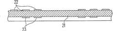
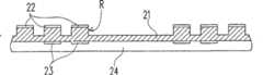
图1A~1E表示为在日本专利申请案公开案第2005-317998号中所公开的一种半导体装置的制作流程剖面示意图。首先,请参看图1A,提供具有一铜箔21,此铜箔21具有分别形成于其上表面及下表面之一作为电性接点的第一图案化金属层22以及一第二图案化金属层23。请参看图1B,于铜箔21的下表面上形成一蚀刻阻抗层24,接着,利用第一图案化金属层22作为一蚀刻掩模(etching mask)对铜箔21的上表面进行一半蚀刻(half-etching)工艺,以于在铜箔21的上表面上形成多个凹部R。之后,请参看图1C,通过使用黏着层20将半导体装置11固定于其中一作为芯片座的凹部R上,且在半导体装置11与铜箔21的打线接合部12之间形成多条导线16。接着,请参看图1D,于铜箔21的上表面上形成一第二绝缘材料18,以包覆半导体装置11、导线16,以及铜箔21的上表面。最后,请参看图1E,利用第二图案化金属层23作为蚀刻掩模对铜箔21的下表面进行背蚀刻工艺,以形成具有面数组引脚(area array lead)的芯片封装结构10。1A-1E are cross-sectional schematic diagrams showing a fabrication process of a semiconductor device disclosed in Japanese Patent Application Publication No. 2005-317998. First, referring to FIG. 1A , a
在日本专利申请案公开案第2005-317998号中所公开的芯片封装结构的制作过程中,需通过背蚀刻工艺来完成整个封装工艺。然而,背蚀刻工艺可能会损坏芯片,进而降低芯片封装结构的良率。因此,如何改良芯片封装结构的制作流程以提升其制作良率,实为亟待解决的一大难题。In the manufacturing process of the chip packaging structure disclosed in Japanese Patent Application Publication No. 2005-317998, the entire packaging process needs to be completed through a back etching process. However, the back etching process may damage the chip, thereby reducing the yield of the chip package structure. Therefore, how to improve the manufacturing process of the chip packaging structure to increase its manufacturing yield is a major problem to be solved urgently.
发明内容Contents of the invention
本发明提供一种芯片封装结构以及其制作方法。在此芯片封装结构的制作方法中,将芯片置放于芯片承载器上之后,不需进行背蚀刻工艺,以保护芯片免于因进行背蚀刻工艺而受到损坏,进而提升芯片封装结构的良率。The invention provides a chip packaging structure and a manufacturing method thereof. In the manufacturing method of the chip packaging structure, after the chip is placed on the chip carrier, no back etching process is required to protect the chip from being damaged due to the back etching process, thereby improving the yield rate of the chip packaging structure .
本发明提出一种芯片封装结构的制作方法,此制作方法包括以下步骤。提供具有第一表面以及与其相对的第二表面的金属板材(metallic plate)。金属板材包括形成于其第一表面上的第一图案化金属层。接着,以第一图案化金属层为一蚀刻掩模对金属板材的第一表面进行一半蚀刻工艺,以在金属板材的第一表面上形成多个第一凹部,其中这些第一凹部是该金属板材定义出多个引脚。接着,在各第一凹部中填充一第一绝缘材料。接着,将第二图案化金属层形成于金属板材的第二表面上。然后,通过使用第二图案化金属层作为蚀刻掩模来对金属板材的第二表面进行半蚀刻工艺,以在金属板材的第二表面上形成多个第二凹部。第二凹部分别对应于第一凹部,且暴露第一凹部内部的第一绝缘材料,使得引脚彼此电性绝缘。接着,将芯片置放在金属板材上。最后,将芯片电性连接至引脚。The invention provides a method for manufacturing a chip packaging structure, and the method includes the following steps. A metallic plate is provided having a first surface and a second surface opposite thereto. The metal sheet includes a first patterned metal layer formed on its first surface. Next, a half-etching process is performed on the first surface of the metal plate by using the first patterned metal layer as an etching mask to form a plurality of first recesses on the first surface of the metal plate, wherein the first recesses are the metal The board defines a number of pins. Next, a first insulating material is filled in each first recess. Next, a second patterned metal layer is formed on the second surface of the metal plate. Then, a half-etching process is performed on the second surface of the metal plate by using the second patterned metal layer as an etching mask to form a plurality of second recesses on the second surface of the metal plate. The second recesses respectively correspond to the first recesses, and expose the first insulating material inside the first recesses, so that the pins are electrically insulated from each other. Next, the chip is placed on the metal plate. Finally, electrically connect the chip to the pins.
在本发明的一实施例中,金属板材为铜箔。In an embodiment of the invention, the metal sheet is copper foil.
在本发明的一实施例中,第一图案化金属层为镍/银层。In an embodiment of the invention, the first patterned metal layer is a nickel/silver layer.
在本发明的一实施例中,第二图案化金属层为镍/银层。In an embodiment of the invention, the second patterned metal layer is a nickel/silver layer.
在本发明的一实施例中,芯片被固定于金属板材的第一表面或第二表面上。In one embodiment of the invention, the chip is fixed on the first surface or the second surface of the metal plate.
在本发明的一实施例中,对金属板材的第一表面进行半蚀刻工艺,以于金属板材的第一表面上形成第一凹部的步骤还包括在金属板材上定义出一芯片座,且这些引脚是围绕芯片座。In an embodiment of the present invention, the step of performing a half-etching process on the first surface of the metal plate to form a first recess on the first surface of the metal plate further includes defining a chip seat on the metal plate, and these The pins are around the chip holder.
在本发明的一实施例中,此芯片是通过一黏着层而固定于芯片座上。In one embodiment of the present invention, the chip is fixed on the chip holder through an adhesive layer.
在本发明的一实施例中,电性连接芯片与引脚的步骤是在芯片与引脚之间形成多个导线,使得芯片经由导线而电性连接至引脚。In an embodiment of the present invention, the step of electrically connecting the chip and the pins is to form a plurality of wires between the chip and the pins, so that the chip is electrically connected to the pins through the wires.
在本发明的一实施例中,电性连接芯片与引脚的步骤是利用倒装芯片接合技术使芯片与这些引脚电性连接。In one embodiment of the present invention, the step of electrically connecting the chip to the pins is to electrically connect the chip to the pins by using flip-chip bonding technology.
在本发明的一实施例中,在电性连接芯片与引脚的步骤之后,此方法还包括在金属板材的第一表面上形成一第二绝缘材料,以包覆芯片以及电性连接芯片与引脚的多个导电组件的步骤。In an embodiment of the present invention, after the step of electrically connecting the chip and the pins, the method further includes forming a second insulating material on the first surface of the metal plate to cover the chip and electrically connect the chip and the lead. Steps for multiple conductive components of pins.
本发明也提供一种芯片封装结构,其包括一芯片承载器、一芯片、多个导电组件、一第一绝缘材料以及一第二绝缘材料。芯片承载器具有一第一表面以及与第一表面相对应的一第二表面,且芯片承载器包括多个引脚。芯片是配置在芯片承载器的第一表面上。导电组件配置于芯片与引脚之间,使芯片透过这些导电组件而与引脚电性连接。第一绝缘材料填充在引脚之间,使得引脚彼此电性绝缘。第二绝缘材料包覆芯片承载器的第一表面、芯片、导电组件,以及第一绝缘材料的一表面。The invention also provides a chip packaging structure, which includes a chip carrier, a chip, a plurality of conductive components, a first insulating material and a second insulating material. The chip carrier has a first surface and a second surface corresponding to the first surface, and the chip carrier includes a plurality of pins. The chip is configured on the first surface of the chip carrier. The conductive components are disposed between the chip and the pins, so that the chip is electrically connected to the pins through the conductive components. The first insulating material is filled between the pins, so that the pins are electrically insulated from each other. The second insulating material covers the first surface of the chip carrier, the chip, the conductive component, and a surface of the first insulating material.
在本发明的一实施例中,芯片承载器还包括一芯片座,且这些引脚是围绕芯片座。In an embodiment of the present invention, the chip carrier further includes a chip seat, and the pins surround the chip seat.
在本发明的一实施例中,芯片具有一有源面、一背面,以及在有源面上的多个芯片焊垫,且芯片的背面是固定于芯片座上。In an embodiment of the present invention, the chip has an active surface, a back surface, and a plurality of chip bonding pads on the active surface, and the back surface of the chip is fixed on the chip holder.
在本发明的一实施例中,导电组件为多条导线,分别连接芯片焊垫与引脚。In an embodiment of the present invention, the conductive component is a plurality of wires, respectively connected to the pads of the chip and the pins.
在本发明的一实施例中,芯片具有一有源面以及在有源面上的多个芯片焊垫,且有源面是面对芯片承载器的第一表面。In an embodiment of the invention, the chip has an active surface and a plurality of chip pads on the active surface, and the active surface is the first surface facing the chip carrier.
在本发明的一实施例中,导电组件为分别配置在引脚与芯片焊垫之间的多个凸块,使得芯片经由凸块而电性连接至芯片承载器。In an embodiment of the present invention, the conductive components are a plurality of bumps disposed between the pins and the pads of the chip, so that the chip is electrically connected to the chip carrier through the bumps.
在本发明的一实施例中,第一绝缘材料填充在引脚之间,且接近芯片承载器的第一表面。In an embodiment of the invention, the first insulating material is filled between the pins and close to the first surface of the chip carrier.
在本发明的一实施例中,第一绝缘材料填充在引脚之间,且接近芯片承载器之第二表面。In an embodiment of the invention, the first insulating material is filled between the pins and close to the second surface of the chip carrier.
在本发明的一实施例中,芯片承载器还包括位于芯片承载器的第一表面上的镍/银层。In an embodiment of the invention, the chip carrier further includes a nickel/silver layer on the first surface of the chip carrier.
在本发明的一实施例中,芯片承载器还包括位于芯片承载器的第二表面上的镍/银层。In an embodiment of the invention, the chip carrier further includes a nickel/silver layer on the second surface of the chip carrier.
在本发明的一实施例中,第一绝缘材料的材料不同于第二绝缘材料的材料。In an embodiment of the present invention, the material of the first insulating material is different from that of the second insulating material.
本发明的芯片封装结构的制造方法主要是利用半蚀刻工艺以及将第一绝缘材料填充于金属板材的凹部中的步骤,以形成具有引脚的芯片承载器。由于将芯片固定于芯片承载器上之后,不需再进行背蚀刻工艺,因此,可保护芯片免于因背蚀刻工艺而受到损坏,进而提升芯片封装结构的良率。The manufacturing method of the chip packaging structure of the present invention mainly utilizes the steps of half-etching process and filling the first insulating material in the concave portion of the metal plate to form the chip carrier with pins. Since the chip is fixed on the chip carrier, no back etching process is required, so the chip can be protected from being damaged by the back etching process, thereby improving the yield rate of the chip packaging structure.
附图说明Description of drawings
图1A~1E所示为在日本专利申请案公开案第2005-317998号中所公开的一种半导体装置的制作流程剖面示意图;1A to 1E are schematic cross-sectional views showing the manufacturing process of a semiconductor device disclosed in Japanese Patent Application Publication No. 2005-317998;
图2A~2I所示为根据本发明的一实施例的一种芯片封装结构的制作流程剖面示意图;2A to 2I are schematic cross-sectional views showing a manufacturing process of a chip packaging structure according to an embodiment of the present invention;
图3所示为将芯片封装结构的金属板材倒置的剖面示意图;FIG. 3 is a schematic cross-sectional view showing an upside-down metal plate of the chip packaging structure;
图4A~4D所示为根据本发明的另一实施例的一种芯片封装结构的制作流程剖面示意图;4A to 4D are schematic cross-sectional views showing a manufacturing process of a chip packaging structure according to another embodiment of the present invention;
图5所示为将芯片封装结构的金属板材倒置的剖面示意图。FIG. 5 is a schematic cross-sectional view of an inverted metal plate of the chip packaging structure.
【主要组件符号说明】[Description of main component symbols]
10:芯片封装结构10: Chip package structure
11:半导体装置11: Semiconductor device
12:线结合部分12: Line bonding part
16:导线16: wire
18:第二绝缘材料18: Second insulating material
20:黏着层20: Adhesive layer
21:铜箔21: copper foil
22:第一图案化金属层22: The first patterned metal layer
23:第二图案化金属层23: Second patterned metal layer
24:蚀刻电阻层24: Etching the resistance layer
110:金属板材110: sheet metal
110’:芯片承载器110': chip carrier
112:引脚112: pin
114:芯片座114: chip seat
122:第一图案化金属层122: first patterned metal layer
124:第二图案化金属层124: second patterned metal layer
130:第一绝缘材料130: first insulating material
140:芯片140: chip
142:有源面142: Active surface
144:背面144: back
146:芯片焊垫146: chip pad
150:黏着层150: Adhesive layer
160:导电组件160: Conductive components
160a:导线160a: Wire
170:第二绝缘材料170: Second insulating material
180:焊球180: solder ball
210:金属板材210: sheet metal
212:引脚212: Pin
230:第一绝缘材料230: first insulating material
240:芯片240: chip
242:有源面242: active surface
244:芯片焊垫244: chip bonding pad
260:导电组件260: Conductive components
260a:凸块260a: Bump
270:第二绝缘材料270: Second insulating material
280:焊球280: solder ball
R:凹部R: Recess
R1:第一凹部R1: first recess
R2:第二凹部R2: second recess
S1:第一表面S1: first surface
S2:第二表面S2: second surface
具体实施方式Detailed ways
图2A~2I所示为根据本发明的一实施例的一种芯片封装结构的制作流程剖面示意图。在此实施例中,芯片与芯片承载器间的电性接方式是以打线接合技术为例以作说明。然而,也可通过倒装芯片技术或其它方式使芯片电性连接至芯片承载器,而此方式将在另一实施例中加以说明。2A-2I are schematic cross-sectional views showing a manufacturing process of a chip packaging structure according to an embodiment of the present invention. In this embodiment, the electrical connection method between the chip and the chip carrier is described by taking wire bonding technology as an example. However, the chip can also be electrically connected to the chip carrier by flip-chip technology or other methods, which will be described in another embodiment.
首先,请参看图2A,提供一金属板材110,此金属板材110具有一第一表面S1以及与第一表面S1相对应的一第二表面S2。金属板材110包括形成于金属板材110的第一表面S1上的一第一图案化金属层122。在本发明的一实施例中,金属板材110为铜箔,且第一图案化金属层122为通过电镀而形成的镍/银层。接着,请参考图2B,利用第一图案化金属层122作为蚀刻掩模对金属板材110的第一表面S1进行半蚀刻工艺,以于金属板材110的第一表面S1上形成多个第一凹部R1,并通过第一凹部R1在金属板材110上定义出多个引脚112。在此实施例中,如图2B中所示的步骤还包括在金属板材110的第一表面S1上定义出一芯片座114,且这些引脚112是围绕芯片座114。接着,请参看图2C,将第一绝缘材料130填充于各第一凹部R1中。第一绝缘材料130的材料可为树脂或其它适当材料。First, please refer to FIG. 2A , a
接着,参看图2D,在金属板材110的第二表面S2上形成一第二图案化金属层124。同样地,第二图案化金属层124可为通过电镀而形成的镍/银层。接着,参看图2E,利用第二图案化金属层124作为一蚀刻掩模对金属板材110的第二表面S2进行一半蚀刻工艺,以于金属板材110的第二表面S2上形成多个第二凹部R2,使金属板材110可作为一芯片承载器110′。如图2E中所示,第二凹部R2分别对应于第一凹部R1,且暴露出第一凹部R1内的第一绝缘材料130,使得引脚112彼此电性绝缘,且使芯片座114与相邻的引脚112电性绝缘。Next, referring to FIG. 2D , a second
接着,请参看图2F,移除芯片座114上的第一图案化金属层122,且接着将一芯片140(例如:半导体装置)配置于芯片承载器110′上。在此实施例中,芯片140具有一有源面142、一背面144,以及多个位于有源面142上的芯片焊垫146,且芯片140的背面144通过一黏着层150固定于芯片座114上。最后,请参看图2G,将芯片140电性连接至引脚112。如图2G中所示,通过打线接合技术在芯片焊垫146与引脚112之间形成多个导电组件160(即导线160a),使得芯片140可经由导线160a与引脚112电性连接。至此,即完成芯片封装结构100的制作流程。此外,各引脚112的底部可作为用于电性连接至外部装置的电性接点。Next, referring to FIG. 2F , the first
除此之外,为保护图2G中所示的芯片座114、引脚112、芯片140,以及导线160a免于受损以及污染,可进行如图2H中所示的步骤。如图2H中所示,于金属板材110的第一表面S1上形成一第二绝缘材料170,以包覆芯片140、第一绝缘材料130的至少一表面以及电性连接芯片140与引脚112的导电组件160(即导线160a)。此外,第二绝缘材料170的材料不同于第一绝缘材料130的材料。再者,在完成上述步骤之后,请参考图2I所示,使用者可选择性地于各引脚112上分别形成一焊球180,使整个芯片封装结构100可透过这些焊球180与其它电子装置电性连接。In addition, in order to protect the
在此实施例中,芯片140是配置于金属板材110的第一表面S1上。然而,如图3中所示,可将金属板材110倒置,使得将芯片140置放于金属板材110的第二表面S2上。本发明对于芯片140相对于金属板材110的位置不作任何限制。In this embodiment, the
请再参考图2I所示,根据以上工艺所形成的芯片封装结构100主要包括芯片一承载器110′、一芯片140、多个导电组件160(即导线160a)、一第一绝缘材料130,以及一第二绝缘材料170。芯片承载器110′具有一第一表面S1以及与第一表面S1相对应的一第二表面S2。芯片承载器110′包括由这些第一凹部R1所定义出的多个引脚112。在此实施例中,芯片承载器110′还包括一芯片座114,且这些引脚112是围绕芯片座114。芯片140是配置于芯片承载器110′的第一表面S1上。导电组件160(即导线160a)是位于芯片140与引脚112之间,以透过导电组件电性连接芯片140与引脚112。第一绝缘材料130填充于引脚112之间,使得引脚112彼此电性绝缘。第二绝缘材料170包覆芯片承载器110′的第一表面S1、芯片140、导电组件160(即导线160a),以及第一绝缘材料130的一表面。芯片封装结构100还包括填充于引脚112之间且邻近于芯片承载器110′的第一表面S1的第一绝缘材料130。然而,当以如图3中所示的倒置方式配置金属板材110时,第一绝缘材料130是位于芯片承载器110′的第二表面S2附近。此外,芯片封装结构100可还包括在芯片承载器110′的第一表面S1及/或第二表面S2上的镍/银层。再者,芯片封装结构100还可包含多个焊球180,分别配置于上述引脚112上,使整个芯片封装结构100可透过这些焊球180与其它电子装置电性连接。Please refer to FIG. 2I again, the
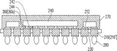
图4A~4D所示为根据本发明的另一实施例的一种芯片封装结构的制作流程剖面示意图。在此实施例中,芯片与芯片承载器间的电性连接方式将以倒装芯片接合技术为例以作说明。首先,提供一根据图2A~2E中所示的步骤制作而成的金属板材210。图2E中所示的芯片承载器100′与图4A中所示的芯片承载器210′之间的差异在于:金属板材210仅包括多个引脚212。接着,请参考图4B,将芯片240配置于金属板材210上,且通过倒装芯片技术将芯片240电性连接至金属板材210。在此实施例中,芯片240具有有源面242以及位于有源面242上的多个芯片焊垫244,且有源面242面对金属板材210的第一表面S 1。此外,芯片240经由配置于芯片240与引脚212间的导电组件260(即凸块260a)电性连接至引脚212。4A-4D are schematic cross-sectional views showing a manufacturing process of a chip packaging structure according to another embodiment of the present invention. In this embodiment, the electrical connection between the chip and the chip carrier will be described by taking the flip-chip bonding technology as an example. First, a
除此之外,为保护图4B中所示的引脚212、芯片240,以及凸块260a免于受损以及污染,可进行如图4C中所示的步骤。如图4C中所示,于金属板材210的第一表面S1上形成一第二绝缘材料270,以包覆芯片240、第一绝缘材料230的一表面以及电性连接芯片240与引脚212的导电组件260(亦即,凸块260a)。除此之外,第二绝缘材料270的材料不同于第一绝缘材料230的材料。再者,在完成上述步骤之后,请参考图4D所示,使用者可选择性地于各引脚212上分别形成一焊球280,使整个芯片封装结构可透过这些焊球280与其它电子装置电性连接。In addition, in order to protect the
同样地,如图5中所示,也可将金属板材210倒置,使得将芯片240配置于金属板材210的第二表面S2上。本发明中对于芯片240相对于金属板材210的位置不作任何限制。Likewise, as shown in FIG. 5 , the
综上所述,本发明所公开的芯片封装结构的制造方法主要是利用半蚀刻工艺以及将第一绝缘材料填充于金属板材的凹部中的步骤来形成具有引脚的芯片承载器。接着,将芯片置放于芯片承载器上,且将其电性连接至芯片承载器,以形成一芯片封装结构。由于将芯片固定于芯片承载器上之后,不需再进行背蚀刻工艺,因此,可保护芯片免于因背蚀刻工艺而受到损坏,进而提升芯片封装结构的良率。To sum up, the manufacturing method of the chip packaging structure disclosed in the present invention mainly uses the half-etching process and the step of filling the first insulating material in the concave portion of the metal plate to form the chip carrier with leads. Then, place the chip on the chip carrier and electrically connect it to the chip carrier to form a chip package structure. Since the chip is fixed on the chip carrier, no back etching process is required, so the chip can be protected from being damaged by the back etching process, thereby improving the yield rate of the chip packaging structure.
虽然本发明已以较优实施例公开如上,然其并非用以限定本发明,任何所属技术领域中具有通常知识者,在不脱离本发明的精神和范围内,当可作些许的还动与润饰,因此本发明的保护范围当视后附的权利要求所界定者为准。Although the present invention has been disclosed above with preferred embodiments, it is not intended to limit the present invention. Anyone with ordinary knowledge in the technical field may make some modifications and changes without departing from the spirit and scope of the present invention. Modification, therefore, the scope of protection of the present invention shall prevail as defined by the appended claims.
Claims (13)
Applications Claiming Priority (2)
| Application Number | Priority Date | Filing Date | Title |
|---|---|---|---|
| US11/941,309 | 2007-11-16 | ||
| US11/941,309US20090127682A1 (en) | 2007-11-16 | 2007-11-16 | Chip package structure and method of fabricating the same |
Publications (2)
| Publication Number | Publication Date |
|---|---|
| CN101252096Atrue CN101252096A (en) | 2008-08-27 |
| CN101252096B CN101252096B (en) | 2010-08-11 |
Family
ID=39955410
Family Applications (1)
| Application Number | Title | Priority Date | Filing Date |
|---|---|---|---|
| CN2008100918395AActiveCN101252096B (en) | 2007-11-16 | 2008-04-03 | Chip packaging structure and manufacturing method thereof |
Country Status (2)
| Country | Link |
|---|---|
| US (1) | US20090127682A1 (en) |
| CN (1) | CN101252096B (en) |
Cited By (12)
| Publication number | Priority date | Publication date | Assignee | Title |
|---|---|---|---|---|
| CN101866867A (en)* | 2010-06-18 | 2010-10-20 | 日月光封装测试(上海)有限公司 | Manufacturing method for lead frame of semiconductor packaging structure with no outer lead |
| CN101944520A (en)* | 2010-09-26 | 2011-01-12 | 日月光半导体制造股份有限公司 | Semiconductor packaging structure and semiconductor packaging process |
| CN101958301A (en)* | 2010-09-04 | 2011-01-26 | 江苏长电科技股份有限公司 | Double-sided graphics chip directly placed in a single packaging structure and its packaging method |
| CN102339762A (en)* | 2010-07-23 | 2012-02-01 | 矽品精密工业股份有限公司 | Carrier-less semiconductor package and manufacturing method thereof |
| CN101859713B (en)* | 2009-04-10 | 2012-05-02 | 日月光半导体制造股份有限公司 | Advanced quad flat no-lead package structure and manufacturing method thereof |
| CN102446775A (en)* | 2010-10-13 | 2012-05-09 | 矽品精密工业股份有限公司 | Carrier-less semiconductor package and manufacturing method thereof |
| CN105161425A (en)* | 2015-07-30 | 2015-12-16 | 南通富士通微电子股份有限公司 | Semiconductor stacked packaging method |
| CN105161424A (en)* | 2015-07-30 | 2015-12-16 | 南通富士通微电子股份有限公司 | Semiconductor stacked packaging method |
| CN105374787A (en)* | 2014-08-15 | 2016-03-02 | 英飞凌科技股份有限公司 | Molded flip-clip semiconductor package |
| CN111564377A (en)* | 2020-05-18 | 2020-08-21 | 无锡中微高科电子有限公司 | Plastic packaging method for frame type integrated circuit |
| CN113571423A (en)* | 2020-07-13 | 2021-10-29 | 台湾积体电路制造股份有限公司 | Semiconductor structure and forming method thereof |
| TWI829115B (en)* | 2015-03-03 | 2024-01-11 | 美商艾馬克科技公司 | Electronic package structure |
Families Citing this family (13)
| Publication number | Priority date | Publication date | Assignee | Title |
|---|---|---|---|---|
| US7727813B2 (en)* | 2007-11-26 | 2010-06-01 | Infineon Technologies Ag | Method for making a device including placing a semiconductor chip on a substrate |
| US8115285B2 (en)* | 2008-03-14 | 2012-02-14 | Advanced Semiconductor Engineering, Inc. | Advanced quad flat no lead chip package having a protective layer to enhance surface mounting and manufacturing methods thereof |
| KR101204092B1 (en)* | 2008-05-16 | 2012-11-22 | 삼성테크윈 주식회사 | Lead frame and semiconductor package and the manufacturing method for the same |
| US20100044850A1 (en)* | 2008-08-21 | 2010-02-25 | Advanced Semiconductor Engineering, Inc. | Advanced quad flat non-leaded package structure and manufacturing method thereof |
| US8803300B2 (en)* | 2009-10-01 | 2014-08-12 | Stats Chippac Ltd. | Integrated circuit packaging system with protective coating and method of manufacture thereof |
| US20110163430A1 (en)* | 2010-01-06 | 2011-07-07 | Advanced Semiconductor Engineering, Inc. | Leadframe Structure, Advanced Quad Flat No Lead Package Structure Using the Same, and Manufacturing Methods Thereof |
| TWI427716B (en) | 2010-06-04 | 2014-02-21 | 矽品精密工業股份有限公司 | Semiconductor package without carrier and method of fabricating the same |
| US8673689B2 (en) | 2011-01-28 | 2014-03-18 | Marvell World Trade Ltd. | Single layer BGA substrate process |
| US8957509B2 (en)* | 2011-06-23 | 2015-02-17 | Stats Chippac Ltd. | Integrated circuit packaging system with thermal emission and method of manufacture thereof |
| US9324584B2 (en)* | 2012-12-14 | 2016-04-26 | Stats Chippac Ltd. | Integrated circuit packaging system with transferable trace lead frame |
| KR101538543B1 (en)* | 2013-08-13 | 2015-07-22 | 앰코 테크놀로지 코리아 주식회사 | Semiconductor Device and Fabricating Method Thereof |
| CN104766832B (en)* | 2014-01-03 | 2020-07-14 | 海成帝爱斯株式会社 | Method of manufacturing semiconductor package substrate and semiconductor package substrate manufactured using the same |
| US9576935B2 (en) | 2014-04-16 | 2017-02-21 | Infineon Technologies Ag | Method for fabricating a semiconductor package and semiconductor package |
Family Cites Families (9)
| Publication number | Priority date | Publication date | Assignee | Title |
|---|---|---|---|---|
| US5656550A (en)* | 1994-08-24 | 1997-08-12 | Fujitsu Limited | Method of producing a semicondutor device having a lead portion with outer connecting terminal |
| CN1196185C (en)* | 2003-05-15 | 2005-04-06 | 王鸿仁 | Second half-etching preparation method of image sensor single-layer lead frame |
| WO2006105733A1 (en)* | 2005-04-07 | 2006-10-12 | Jiangsu Changjiang Electronics Technology Co., Ltd. | Package structure with flat bumps for electronic device and method of manufacture the same |
| KR101089449B1 (en)* | 2005-08-10 | 2011-12-07 | 가부시키가이샤 미츠이하이테크 | Semiconductor device and method for manufacturing same |
| CN100433320C (en)* | 2005-10-28 | 2008-11-12 | 南茂科技股份有限公司 | Chip packaging structure and bump manufacturing process |
| US20080029855A1 (en)* | 2006-08-04 | 2008-02-07 | Yi-Ling Chang | Lead Frame and Fabrication Method thereof |
| US8124461B2 (en)* | 2006-12-27 | 2012-02-28 | Mediatek Inc. | Method for manufacturing leadframe, packaging method for using the leadframe and semiconductor package product |
| CN100555592C (en)* | 2007-02-08 | 2009-10-28 | 百慕达南茂科技股份有限公司 | Chip-packaging structure and preparation method thereof |
| CN100539054C (en)* | 2007-03-13 | 2009-09-09 | 百慕达南茂科技股份有限公司 | Chip-packaging structure and preparation method thereof |
- 2007
- 2007-11-16USUS11/941,309patent/US20090127682A1/ennot_activeAbandoned
- 2008
- 2008-04-03CNCN2008100918395Apatent/CN101252096B/enactiveActive
Cited By (21)
| Publication number | Priority date | Publication date | Assignee | Title |
|---|---|---|---|---|
| CN101859713B (en)* | 2009-04-10 | 2012-05-02 | 日月光半导体制造股份有限公司 | Advanced quad flat no-lead package structure and manufacturing method thereof |
| CN101859740B (en)* | 2009-04-10 | 2012-05-02 | 日月光半导体制造股份有限公司 | Advanced quad flat no-lead package structure and manufacturing method thereof |
| CN101866867A (en)* | 2010-06-18 | 2010-10-20 | 日月光封装测试(上海)有限公司 | Manufacturing method for lead frame of semiconductor packaging structure with no outer lead |
| CN102339762B (en)* | 2010-07-23 | 2013-09-04 | 矽品精密工业股份有限公司 | Submountless semiconductor package and manufacturing method thereof |
| CN102339762A (en)* | 2010-07-23 | 2012-02-01 | 矽品精密工业股份有限公司 | Carrier-less semiconductor package and manufacturing method thereof |
| CN101958301A (en)* | 2010-09-04 | 2011-01-26 | 江苏长电科技股份有限公司 | Double-sided graphics chip directly placed in a single packaging structure and its packaging method |
| CN101944520A (en)* | 2010-09-26 | 2011-01-12 | 日月光半导体制造股份有限公司 | Semiconductor packaging structure and semiconductor packaging process |
| CN101944520B (en)* | 2010-09-26 | 2012-06-27 | 日月光半导体制造股份有限公司 | Semiconductor packaging structure and semiconductor packaging process |
| CN102446775A (en)* | 2010-10-13 | 2012-05-09 | 矽品精密工业股份有限公司 | Carrier-less semiconductor package and manufacturing method thereof |
| CN102446775B (en)* | 2010-10-13 | 2014-03-12 | 矽品精密工业股份有限公司 | Submountless semiconductor package and manufacturing method thereof |
| CN105374787A (en)* | 2014-08-15 | 2016-03-02 | 英飞凌科技股份有限公司 | Molded flip-clip semiconductor package |
| CN105374787B (en)* | 2014-08-15 | 2018-09-21 | 英飞凌科技股份有限公司 | Mould flip chip semiconductor package body |
| TWI829115B (en)* | 2015-03-03 | 2024-01-11 | 美商艾馬克科技公司 | Electronic package structure |
| TWI880876B (en)* | 2015-03-03 | 2025-04-11 | 新加坡商安靠科技新加坡控股私人有限公司 | Electronic package structure |
| TWI867901B (en)* | 2015-03-03 | 2024-12-21 | 新加坡商安靠科技新加坡控股私人有限公司 | Electronic package structure |
| CN105161425A (en)* | 2015-07-30 | 2015-12-16 | 南通富士通微电子股份有限公司 | Semiconductor stacked packaging method |
| CN105161424A (en)* | 2015-07-30 | 2015-12-16 | 南通富士通微电子股份有限公司 | Semiconductor stacked packaging method |
| CN111564377B (en)* | 2020-05-18 | 2023-08-11 | 无锡中微高科电子有限公司 | Plastic packaging method of frame type integrated circuit |
| CN111564377A (en)* | 2020-05-18 | 2020-08-21 | 无锡中微高科电子有限公司 | Plastic packaging method for frame type integrated circuit |
| CN113571423A (en)* | 2020-07-13 | 2021-10-29 | 台湾积体电路制造股份有限公司 | Semiconductor structure and forming method thereof |
| US12057418B2 (en) | 2020-07-13 | 2024-08-06 | Taiwan Semiconductor Manufacturing Co., Ltd. | Passivation structure with increased thickness for metal pads |
Also Published As
| Publication number | Publication date |
|---|---|
| CN101252096B (en) | 2010-08-11 |
| US20090127682A1 (en) | 2009-05-21 |
Similar Documents
| Publication | Publication Date | Title |
|---|---|---|
| CN101252096A (en) | Chip packaging structure and manufacturing method thereof | |
| CN100499052C (en) | Planar grid array packaging device and manufacturing method thereof | |
| US8487424B2 (en) | Routable array metal integrated circuit package fabricated using partial etching process | |
| CN102201385B (en) | Quad flat no-lead semiconductor package and manufacturing method thereof | |
| US8154110B2 (en) | Double-faced electrode package and its manufacturing method | |
| JP5227501B2 (en) | Stack die package and method of manufacturing the same | |
| TWI404175B (en) | Semiconductor package having electrical connecting structures and fabrication method thereof | |
| US7834469B2 (en) | Stacked type chip package structure including a chip package and a chip that are stacked on a lead frame | |
| US20090278243A1 (en) | Stacked type chip package structure and method for fabricating the same | |
| US20160064310A1 (en) | Semiconductor package having routing traces therein | |
| CN102456648B (en) | Method for manufacturing package substrate | |
| KR20060126645A (en) | How to package an integrated circuit die | |
| CN105990268B (en) | Electronic package structure and method for fabricating the same | |
| US20090206459A1 (en) | Quad flat non-leaded package structure | |
| CN101290929B (en) | Stack type chip packaging structure | |
| US6160311A (en) | Enhanced heat dissipating chip scale package method and devices | |
| TWI651827B (en) | Substrate-free package structure | |
| TWI595616B (en) | Chip package and method of forming same | |
| CN100466246C (en) | Flexible Substrates for Packaging | |
| TWI590349B (en) | Chip package and chip packaging process | |
| CN102130085B (en) | Semiconductor package with electrical connection structure and manufacturing method thereof | |
| US20250167065A1 (en) | Semiconductor package including heat dissipation member, and method for manufacturing the same | |
| CN102496608A (en) | Semiconductor package with engaging portion and manufacturing method thereof | |
| KR20100069001A (en) | Semiconductor package | |
| CN101587884A (en) | Stacked chip packaging structure and manufacturing method thereof |
Legal Events
| Date | Code | Title | Description |
|---|---|---|---|
| C06 | Publication | ||
| PB01 | Publication | ||
| C10 | Entry into substantive examination | ||
| SE01 | Entry into force of request for substantive examination | ||
| C14 | Grant of patent or utility model | ||
| GR01 | Patent grant |