CN101251617A - Method for producing microstructures - Google Patents
Method for producing microstructuresDownload PDFInfo
- Publication number
- CN101251617A CN101251617ACN200810080736.9ACN200810080736ACN101251617ACN 101251617 ACN101251617 ACN 101251617ACN 200810080736 ACN200810080736 ACN 200810080736ACN 101251617 ACN101251617 ACN 101251617A
- Authority
- CN
- China
- Prior art keywords
- light
- denatured
- manufacture method
- region
- denatured areas
- Prior art date
- Legal status (The legal status is an assumption and is not a legal conclusion. Google has not performed a legal analysis and makes no representation as to the accuracy of the status listed.)
- Pending
Links
- 238000004519manufacturing processMethods0.000titleclaimsabstractdescription40
- 238000005530etchingMethods0.000claimsdescription39
- 238000000034methodMethods0.000claimsdescription27
- 229910052782aluminiumInorganic materials0.000claimsdescription22
- XAGFODPZIPBFFR-UHFFFAOYSA-NaluminiumChemical compound[Al]XAGFODPZIPBFFR-UHFFFAOYSA-N0.000claimsdescription22
- 229910018110Se—TeInorganic materials0.000claimsdescription12
- 230000008859changeEffects0.000claimsdescription11
- 229910010272inorganic materialInorganic materials0.000claimsdescription11
- 239000011147inorganic materialSubstances0.000claimsdescription11
- 229910052751metalInorganic materials0.000claimsdescription11
- 239000002184metalSubstances0.000claimsdescription11
- 229910004298SiO 2Inorganic materials0.000claimsdescription5
- 229910005939Ge—SnInorganic materials0.000claimsdescription4
- 229910052718tinInorganic materials0.000claimsdescription4
- 229910018731Sn—AuInorganic materials0.000claimsdescription2
- 239000004411aluminiumSubstances0.000claims1
- 230000001678irradiating effectEffects0.000abstractdescription24
- 238000005516engineering processMethods0.000abstractdescription3
- 239000010408filmSubstances0.000description66
- 238000000926separation methodMethods0.000description20
- 239000000463materialSubstances0.000description17
- MUMZUERVLWJKNR-UHFFFAOYSA-NoxoplatinumChemical compound[Pt]=OMUMZUERVLWJKNR-UHFFFAOYSA-N0.000description17
- 229910003446platinum oxideInorganic materials0.000description17
- 230000010287polarizationEffects0.000description16
- 238000000576coating methodMethods0.000description15
- 238000010586diagramMethods0.000description15
- 230000003287optical effectEffects0.000description15
- 239000000758substrateSubstances0.000description15
- 239000011248coating agentSubstances0.000description14
- 238000009826distributionMethods0.000description13
- 230000000737periodic effectEffects0.000description9
- 230000010363phase shiftEffects0.000description7
- 229920002120photoresistant polymerPolymers0.000description7
- 230000007704transitionEffects0.000description7
- VYPSYNLAJGMNEJ-UHFFFAOYSA-NSilicium dioxideChemical compoundO=[Si]=OVYPSYNLAJGMNEJ-UHFFFAOYSA-N0.000description6
- 239000002994raw materialSubstances0.000description6
- 239000000243solutionSubstances0.000description5
- 238000002834transmittanceMethods0.000description5
- 239000003513alkaliSubstances0.000description4
- 238000002425crystallisationMethods0.000description4
- 230000008025crystallizationEffects0.000description4
- 238000004925denaturationMethods0.000description4
- 230000036425denaturationEffects0.000description4
- 239000000126substanceSubstances0.000description4
- 239000010409thin filmSubstances0.000description4
- 239000013078crystalSubstances0.000description3
- 239000011521glassSubstances0.000description3
- 230000002452interceptive effectEffects0.000description3
- 239000002086nanomaterialSubstances0.000description3
- 230000008569processEffects0.000description3
- 238000004904shorteningMethods0.000description3
- 238000010521absorption reactionMethods0.000description2
- 238000007687exposure techniqueMethods0.000description2
- 229910052737goldInorganic materials0.000description2
- 239000010453quartzSubstances0.000description2
- 239000004065semiconductorSubstances0.000description2
- 238000000992sputter etchingMethods0.000description2
- 230000009471actionEffects0.000description1
- 239000007864aqueous solutionSubstances0.000description1
- 239000002585baseSubstances0.000description1
- 230000015572biosynthetic processEffects0.000description1
- 230000000903blocking effectEffects0.000description1
- 230000001427coherent effectEffects0.000description1
- 238000004455differential thermal analysisMethods0.000description1
- 238000001312dry etchingMethods0.000description1
- 230000000694effectsEffects0.000description1
- 238000010438heat treatmentMethods0.000description1
- 230000002427irreversible effectEffects0.000description1
- 239000004973liquid crystal related substanceSubstances0.000description1
- 238000001459lithographyMethods0.000description1
- 238000005259measurementMethods0.000description1
- 238000002844meltingMethods0.000description1
- 230000008018meltingEffects0.000description1
- 230000009022nonlinear effectEffects0.000description1
- 239000011368organic materialSubstances0.000description1
- 230000000704physical effectEffects0.000description1
- 230000002265preventionEffects0.000description1
- 238000012545processingMethods0.000description1
- 230000004044responseEffects0.000description1
- 229910052709silverInorganic materials0.000description1
- 239000004332silverSubstances0.000description1
- 238000012546transferMethods0.000description1
- 230000009466transformationEffects0.000description1
Images


Classifications
- C—CHEMISTRY; METALLURGY
- C03—GLASS; MINERAL OR SLAG WOOL
- C03C—CHEMICAL COMPOSITION OF GLASSES, GLAZES OR VITREOUS ENAMELS; SURFACE TREATMENT OF GLASS; SURFACE TREATMENT OF FIBRES OR FILAMENTS MADE FROM GLASS, MINERALS OR SLAGS; JOINING GLASS TO GLASS OR OTHER MATERIALS
- C03C15/00—Surface treatment of glass, not in the form of fibres or filaments, by etching
- C—CHEMISTRY; METALLURGY
- C03—GLASS; MINERAL OR SLAG WOOL
- C03C—CHEMICAL COMPOSITION OF GLASSES, GLAZES OR VITREOUS ENAMELS; SURFACE TREATMENT OF GLASS; SURFACE TREATMENT OF FIBRES OR FILAMENTS MADE FROM GLASS, MINERALS OR SLAGS; JOINING GLASS TO GLASS OR OTHER MATERIALS
- C03C17/00—Surface treatment of glass, not in the form of fibres or filaments, by coating
- C03C17/06—Surface treatment of glass, not in the form of fibres or filaments, by coating with metals
- C—CHEMISTRY; METALLURGY
- C03—GLASS; MINERAL OR SLAG WOOL
- C03C—CHEMICAL COMPOSITION OF GLASSES, GLAZES OR VITREOUS ENAMELS; SURFACE TREATMENT OF GLASS; SURFACE TREATMENT OF FIBRES OR FILAMENTS MADE FROM GLASS, MINERALS OR SLAGS; JOINING GLASS TO GLASS OR OTHER MATERIALS
- C03C17/00—Surface treatment of glass, not in the form of fibres or filaments, by coating
- C03C17/34—Surface treatment of glass, not in the form of fibres or filaments, by coating with at least two coatings having different compositions
- C03C17/36—Surface treatment of glass, not in the form of fibres or filaments, by coating with at least two coatings having different compositions at least one coating being a metal
- C03C17/3602—Surface treatment of glass, not in the form of fibres or filaments, by coating with at least two coatings having different compositions at least one coating being a metal the metal being present as a layer
- C03C17/3605—Coatings of the type glass/metal/inorganic compound
- C—CHEMISTRY; METALLURGY
- C03—GLASS; MINERAL OR SLAG WOOL
- C03C—CHEMICAL COMPOSITION OF GLASSES, GLAZES OR VITREOUS ENAMELS; SURFACE TREATMENT OF GLASS; SURFACE TREATMENT OF FIBRES OR FILAMENTS MADE FROM GLASS, MINERALS OR SLAGS; JOINING GLASS TO GLASS OR OTHER MATERIALS
- C03C17/00—Surface treatment of glass, not in the form of fibres or filaments, by coating
- C03C17/34—Surface treatment of glass, not in the form of fibres or filaments, by coating with at least two coatings having different compositions
- C03C17/36—Surface treatment of glass, not in the form of fibres or filaments, by coating with at least two coatings having different compositions at least one coating being a metal
- C03C17/3602—Surface treatment of glass, not in the form of fibres or filaments, by coating with at least two coatings having different compositions at least one coating being a metal the metal being present as a layer
- C03C17/3649—Surface treatment of glass, not in the form of fibres or filaments, by coating with at least two coatings having different compositions at least one coating being a metal the metal being present as a layer made of metals other than silver
- C—CHEMISTRY; METALLURGY
- C03—GLASS; MINERAL OR SLAG WOOL
- C03C—CHEMICAL COMPOSITION OF GLASSES, GLAZES OR VITREOUS ENAMELS; SURFACE TREATMENT OF GLASS; SURFACE TREATMENT OF FIBRES OR FILAMENTS MADE FROM GLASS, MINERALS OR SLAGS; JOINING GLASS TO GLASS OR OTHER MATERIALS
- C03C17/00—Surface treatment of glass, not in the form of fibres or filaments, by coating
- C03C17/34—Surface treatment of glass, not in the form of fibres or filaments, by coating with at least two coatings having different compositions
- C03C17/36—Surface treatment of glass, not in the form of fibres or filaments, by coating with at least two coatings having different compositions at least one coating being a metal
- C03C17/3602—Surface treatment of glass, not in the form of fibres or filaments, by coating with at least two coatings having different compositions at least one coating being a metal the metal being present as a layer
- C03C17/3657—Surface treatment of glass, not in the form of fibres or filaments, by coating with at least two coatings having different compositions at least one coating being a metal the metal being present as a layer the multilayer coating having optical properties
- C—CHEMISTRY; METALLURGY
- C03—GLASS; MINERAL OR SLAG WOOL
- C03C—CHEMICAL COMPOSITION OF GLASSES, GLAZES OR VITREOUS ENAMELS; SURFACE TREATMENT OF GLASS; SURFACE TREATMENT OF FIBRES OR FILAMENTS MADE FROM GLASS, MINERALS OR SLAGS; JOINING GLASS TO GLASS OR OTHER MATERIALS
- C03C23/00—Other surface treatment of glass not in the form of fibres or filaments
- C03C23/0005—Other surface treatment of glass not in the form of fibres or filaments by irradiation
- C03C23/0025—Other surface treatment of glass not in the form of fibres or filaments by irradiation by a laser beam
- C—CHEMISTRY; METALLURGY
- C03—GLASS; MINERAL OR SLAG WOOL
- C03C—CHEMICAL COMPOSITION OF GLASSES, GLAZES OR VITREOUS ENAMELS; SURFACE TREATMENT OF GLASS; SURFACE TREATMENT OF FIBRES OR FILAMENTS MADE FROM GLASS, MINERALS OR SLAGS; JOINING GLASS TO GLASS OR OTHER MATERIALS
- C03C2217/00—Coatings on glass
- C03C2217/20—Materials for coating a single layer on glass
- C03C2217/25—Metals
- C03C2217/251—Al, Cu, Mg or noble metals
- C03C2217/252—Al
- C—CHEMISTRY; METALLURGY
- C03—GLASS; MINERAL OR SLAG WOOL
- C03C—CHEMICAL COMPOSITION OF GLASSES, GLAZES OR VITREOUS ENAMELS; SURFACE TREATMENT OF GLASS; SURFACE TREATMENT OF FIBRES OR FILAMENTS MADE FROM GLASS, MINERALS OR SLAGS; JOINING GLASS TO GLASS OR OTHER MATERIALS
- C03C2217/00—Coatings on glass
- C03C2217/70—Properties of coatings
- C03C2217/73—Anti-reflective coatings with specific characteristics
- G—PHYSICS
- G02—OPTICS
- G02B—OPTICAL ELEMENTS, SYSTEMS OR APPARATUS
- G02B27/00—Optical systems or apparatus not provided for by any of the groups G02B1/00 - G02B26/00, G02B30/00
- G02B27/28—Optical systems or apparatus not provided for by any of the groups G02B1/00 - G02B26/00, G02B30/00 for polarising
- G02B27/283—Optical systems or apparatus not provided for by any of the groups G02B1/00 - G02B26/00, G02B30/00 for polarising used for beam splitting or combining
- G—PHYSICS
- G02—OPTICS
- G02B—OPTICAL ELEMENTS, SYSTEMS OR APPARATUS
- G02B5/00—Optical elements other than lenses
- G02B5/30—Polarising elements
- G02B5/3083—Birefringent or phase retarding elements
Landscapes
- Chemical & Material Sciences (AREA)
- Life Sciences & Earth Sciences (AREA)
- Engineering & Computer Science (AREA)
- Chemical Kinetics & Catalysis (AREA)
- General Chemical & Material Sciences (AREA)
- Geochemistry & Mineralogy (AREA)
- Materials Engineering (AREA)
- Organic Chemistry (AREA)
- Physics & Mathematics (AREA)
- Optics & Photonics (AREA)
- Health & Medical Sciences (AREA)
- Toxicology (AREA)
- Inorganic Chemistry (AREA)
- Exposure And Positioning Against Photoresist Photosensitive Materials (AREA)
- Diffracting Gratings Or Hologram Optical Elements (AREA)
- Polarising Elements (AREA)
- Lasers (AREA)
Abstract
Translated fromChinese
Description
Translated fromChinese技术领域technical field
本发明涉及使用了激光干涉曝光的微细构造体,尤其涉及一种具有纳米级构造的构造物(纳米构造体)的制造技术。能够应用该技术制造偏光分离元件、相位延迟元件、反射防止元件等各种纳米构造体。The present invention relates to a microstructure using laser interference exposure, and more particularly to a technique for manufacturing a structure (nanostructure) having a nanoscale structure. This technology can be used to manufacture various nanostructures such as polarization separation elements, phase retardation elements, and antireflection elements.
背景技术Background technique
向比可视光的波长(大致380~780nm程度)小的等级的构造物(亚(sub)波长构造体)入射光时,会出现偏光分离、双折射、反射防止、等离子传播等现象。作为用于制造这种亚波长构造体的手段之一,公知的是利用了激光干涉的曝光技术(例如参照专利文献1)。在专利文献1所记载的曝光技术中,通过利用使两束激光束交叉而得到的干涉光(具有干涉条纹的光)对感光性膜进行曝光。此时,由利用了干涉光的曝光形成的图案的周期依存于激光束的波长λ及激光束的交叉角度。理论上,通过干涉曝光能够实现的最小周期等于λ/2。例如,在波长为266nm时,可形成的图案的最小周期理论上为133nm。When light enters a structure (sub-wavelength structure) smaller than the wavelength of visible light (approximately 380 to 780nm), phenomena such as polarization separation, birefringence, reflection prevention, and plasma propagation occur. As one of means for producing such a subwavelength structure, an exposure technique using laser interference is known (for example, refer to Patent Document 1). In the exposure technique described in
根据上述的干涉曝光,为了实现更小的周期的图案,则必须缩短激光束的波长。但是,现状却难以使激光束进一步短波长化。其原因之一是不存在具有比266nm足够短的波长的高相干(coherent)的激光光源。虽然在半导体平版印刷等领域中利用的受激准分子激光器有波长为193nm、157nm等的激光器,但现实情况是其相干不够高,因此,难以形成清晰的潜像图案。另一个理由是当波长比200nm短时,在大气中进行曝光比较困难。另外,也难以求得构成激光干涉曝光系统的光学部件(透镜、反射镜等)所适宜的材料。例如,因为石英玻璃的吸收端位于180nm附近。因而,迫切希望不必过度地追求激光束的进一步短波长化,就可以形成清晰的潜像图案,并用其实现精细图案的技术。According to the above-mentioned interference exposure, in order to realize a pattern with a smaller period, it is necessary to shorten the wavelength of the laser beam. However, it is difficult to further shorten the wavelength of the laser beam under the current situation. One of the reasons for this is that there is no highly coherent laser light source having a sufficiently shorter wavelength than 266 nm. Excimer lasers used in fields such as semiconductor lithography have wavelengths of 193nm and 157nm, but the actual situation is that their coherence is not high enough, so it is difficult to form a clear latent image pattern. Another reason is that exposure in the atmosphere is difficult when the wavelength is shorter than 200nm. In addition, it is also difficult to obtain suitable materials for optical components (lenses, mirrors, etc.) constituting the laser interference exposure system. For example, because the absorption end of quartz glass is located near 180nm. Therefore, there is an urgent need for a technology that can form a clear latent image pattern without excessive pursuit of further shortening the wavelength of the laser beam, and realize a fine pattern using it.
专利文献1:特开2006-093644号公报Patent Document 1: JP-A-2006-093644
发明内容Contents of the invention
鉴于此,本发明的目的之一是提供一种可以实现分辨率高的微细构造体的技术。In view of this, one of the objects of the present invention is to provide a technique capable of realizing a fine structure with high resolution.
本发明的一个方式(下面,为方便起见称作“第一方式”)的微细构造体的制造方法包括:A method of manufacturing a microstructure according to one mode of the present invention (hereinafter, referred to as "the first mode" for convenience) includes:
(a)通过使两束激光束交叉而产生含有干涉条纹的第一光;(a) generating a first light comprising interference fringes by intersecting two laser beams;
(b)对具有热非线性特性的对象物照射所述第一光,由此,在所述对象物上形成与所述第一光的所述干涉条纹的周期相对应而配置的变性区域和非变性区域;(b) irradiating an object having a thermal nonlinear characteristic with the first light, thereby forming denatured regions arranged corresponding to the periods of the interference fringes of the first light on the object and non-denaturing region;
(c)对所述对象物进行蚀刻,选择性地除去所述变性区域或所述非变性区域的任意一个。(c) Etching the object to selectively remove either the denatured region or the non-denatured region.
其中,“具有热非线性特性的对象物”是由PtO、ZnS-SiO2、Ge-Sb-Te、Ge-Sb-Te-S、Te-TeO2-Ge-Sn、Te-Ge-Sn-Au、Ge-Te-Sn、Sn-Se-Te、Sb-Se-Te、Sb-Se、Ga-Se-Te-Ge、In-Se、In-Se-Tl-Co、Ge-Sb-Te、In-Se-Te、Ag-In-Sb-Te、TeO2-Pb等材料构成的基体材料(基板)、被膜、构造物等。另外,“变性区域”例如是结晶状态的区域,“非变性区域”例如是非结晶状态的区域。Among them, the "object having thermal nonlinear characteristics" is composed of PtO, ZnS-SiO2 , Ge-Sb-Te, Ge-Sb-Te-S, Te-TeO2 -Ge-Sn, Te-Ge-Sn- Au, Ge-Te-Sn, Sn-Se-Te, Sb-Se-Te, Sb-Se, Ga-Se-Te-Ge, In-Se, In-Se-Tl-Co, Ge-Sb-Te, Base materials (substrates), coatings, structures, etc. made of materials such as In-Se-Te, Ag-In-Sb-Te, and TeO2 -Pb. In addition, the "denatured region" is, for example, a region in a crystalline state, and the "non-denatured region" is, for example, a region in an amorphous state.
在第一方式中,对具有热非线性特性的对象物照射具有干涉条纹(即光强度分布)的第一光,由此,与光强度相对高的区域和低的区域对应可获得变性区域和非变性区域。该变性区域和非变性区域的循环周期(间距)可以通过缩短所交叉的两束激光束的波长,或增大交叉角度来缩短。通过采用了具有热非线性特性的对象物,即使进一步缩小变性区域和非变性区域的循环周期(例如100nm~200nm程度),与现有的采用光致抗蚀剂膜等的情况相比,也可以清晰地得到变性区域和非变性区域的边界。而且,由于在变性区域和非变性区域之间蚀刻速度产生差异,因此,通过对对象物进行蚀刻,可以形成分辨率高的微细构造体。In the first mode, the first light having interference fringes (i.e., light intensity distribution) is irradiated to an object having thermal nonlinear characteristics, whereby denaturation regions and regions corresponding to relatively high and low light intensity regions can be obtained. non-denaturing region. The cycle period (distance) between the denatured area and the non-denatured area can be shortened by shortening the wavelengths of the two laser beams crossed, or increasing the crossing angle. By using an object with thermal nonlinear characteristics, even if the cycle period between the denatured area and the non-denatured area is further reduced (for example, about 100nm to 200nm), compared with the conventional photoresist film, etc. The boundary between the denatured area and the non-denatured area can be clearly obtained. Furthermore, since there is a difference in etching rate between the denatured region and the non-denatured region, a fine structure with high resolution can be formed by etching the object.
优选所述第一方式的制造方法在所述(b)之后(c)之前还包括:Preferably, the manufacturing method of the first mode further includes after (b) and before (c):
(d)在所述两束激光束之间赋予相位差使该两束激光束交叉,由此产生含有干涉条纹的第二光;(d) imparting a phase difference between the two laser beams so that the two laser beams intersect, thereby generating second light comprising interference fringes;
(e)通过对所述对象物照射所述第二光,形成与所述第二光的所述干涉条纹的周期相对应而配置的变性区域和非变性区域。(e) By irradiating the object with the second light, denatured regions and non-denatured regions arranged corresponding to the periods of the interference fringes of the second light are formed.
通过在两束激光束之间给予相位差,能够使第一光的干涉条纹和第二光的干涉条纹以微小的宽度(例如1/2间距、1/4间距等)错开。通过使这样的第一光和第二光依次向具有热非线性特性的对象物进行照射,能够进一步减小变性区域和非变性区域的循环周期。这样,即使在循环周期进一步减小的情况下,由于使用了具有热非线性特性的对象物,所以,也可清晰地得到变性区域和非变性区域的边界。从而,可以得到分辨率更高的微细构造体。By providing a phase difference between the two laser beams, the interference fringes of the first light and the interference fringes of the second light can be shifted by a small width (for example, 1/2 pitch, 1/4 pitch, etc.). By sequentially irradiating an object having thermal nonlinear characteristics with such first light and second light, the cycle period between the denatured area and the non-denatured area can be further reduced. In this way, even when the cycle period is further reduced, the boundary between the denaturation region and the non-denaturation region can be clearly obtained because an object having thermal nonlinear characteristics is used. Accordingly, a fine structure with higher resolution can be obtained.
在所述第一方式的制造方法中,优选所述(b)使第三光和所述第一光一并向所述对象物进行照射。同样,优选所述(d)使第三光和所述第二光一并向所述对象物进行照射。作为“第三光”,适宜的是例如激光束(激光)等单一波长的光,不过,含有多种波长成分的光也可以。In the manufacturing method of the first aspect, it is preferable in the (b) to irradiate the object with the third light together with the first light. Likewise, in (d), it is preferable to irradiate the object with the third light and the second light together. As the "third light", for example, light of a single wavelength such as a laser beam (laser light) is suitable, but light containing multiple wavelength components may also be used.
在照射第一光或第二光时,通过进一步照射与它们不同的第三光,可以对光照射强度施加偏置。由此,即便在第一光或第二光的光强度低的情况下,也能够可靠地形成变性区域及非变性区域。When the first light or the second light is irradiated, by further irradiating the third light different from these, it is possible to bias the light irradiation intensity. Accordingly, even when the light intensity of the first light or the second light is low, the denatured region and the non-denatured region can be reliably formed.
本发明的另一方式(下面为了方便起见,称作“第二方式”)的微细构造体的制造方法包括:Another mode of the present invention (hereinafter referred to as "second mode" for convenience) is a method for manufacturing a microstructure including:
(a)在对象物上形成具有热非线性特性的被膜;(a) Forming a coating having thermal nonlinear characteristics on an object;
(b)通过使两束激光束交叉而产生含有干涉条纹的第一光;(b) generating a first light comprising interference fringes by intersecting two laser beams;
(c)向所述被膜照射所述第一光,由此,在所述被膜上形成与所述第一光的所述干涉条纹的周期相对应而配置的变性区域和非变性区域;(c) irradiating the coating with the first light, thereby forming denatured regions and non-denatured regions arranged corresponding to the periods of the interference fringes of the first light on the coating;
(d)对所述被膜进行蚀刻,选择性地除去所述变性区域或所述非变性区域的任意一个。(d) Etching the film to selectively remove either the denatured region or the non-denatured region.
(e)经由除去了所述变性区域或所述非变性区域的任意一个之后的所述被膜,进行对所述对象物的蚀刻。(e) Etching the target object through the film after removing either the denatured region or the non-denatured region.
其中,所谓“具有热非线性特性的被膜”是由PtO、ZnS-SiO2、Ge-Sb-Te、Ge-Sb-Te-S、Te-TeO2-Ge-Sn、Te-Ge-Sn-Au、Ge-Te-Sn、Sn-Se-Te、Sb-Se-Te、Sb-Se、Ga-Se-Te-Ge、In-Se、In-Se-Tl-Co、Ge-Sb-Te、In-Se-Te、Ag-In-Sb-Te、TeO2-Pb等材料构成的被膜(薄膜或厚膜)。另外,“变性区域”例如是结晶状态的区域,“非变性区域”例如是非结晶状态的区域。Among them, the so-called "coating with thermal nonlinear characteristics" is made of PtO, ZnS-SiO2 , Ge-Sb-Te, Ge-Sb-Te-S, Te-TeO2 -Ge-Sn, Te-Ge-Sn- Au, Ge-Te-Sn, Sn-Se-Te, Sb-Se-Te, Sb-Se, Ga-Se-Te-Ge, In-Se, In-Se-Tl-Co, Ge-Sb-Te, Coating (thin film or thick film) made of In-Se-Te, Ag-In-Sb-Te, TeO2 -Pb and other materials. In addition, the "denatured region" is, for example, a region in a crystalline state, and the "non-denatured region" is, for example, a region in an amorphous state.
在所述第二方式中,对具有热非线性特性的被膜照射具有干涉条纹的第一光,由此,与光强度相对高的区域和低的区域对应可获得变性区域和非变性区域。该变性区域和非变性区域的循环周期(间距)可以通过减小所交叉的两束激光束的波长,或增大交叉角度来缩短。通过采用了具有热非线性特性的被膜,即便进一步减小变性区域和非变性区域的循环周期(例如100nm~200nm程度),与现有的采用光致抗蚀剂膜等的情况相比,也可以清晰地得到变性区域和非变性区域的边界。而且,由于在变性区域和非变性区域之间蚀刻速度产生差异,因此,通过对被膜进行蚀刻,可以除去变性区域或非变性区域,使相应区域开口。利用具有这样得到的开口的被膜作为蚀刻掩模,进行对对象物的蚀刻,由此,可以形成分辨率高的微细构造体。In the second aspect, the first light having interference fringes is irradiated to the film having thermal nonlinear characteristics, thereby obtaining denatured areas and non-denatured areas corresponding to areas with relatively high light intensity and areas with low light intensity. The cycle period (distance) between the denatured area and the non-denatured area can be shortened by reducing the wavelengths of the two laser beams intersected, or increasing the intersecting angle. By using a film with thermal nonlinear characteristics, even if the cycle period between the denatured area and the non-denatured area is further reduced (for example, about 100nm to 200nm), compared with the conventional photoresist film, etc. The boundary between the denatured area and the non-denatured area can be clearly obtained. Furthermore, since there is a difference in etching rate between the denatured area and the non-denatured area, the denatured area or the non-denatured area can be removed by etching the film, and the corresponding area can be opened. By using the film having the openings obtained in this way as an etching mask, the object is etched, whereby a fine structure with high resolution can be formed.
优选所述第二方式在所述(c)之后(d)之前还包括:Preferably, the second method further includes after (c) and before (d):
(f)在所述两束激光束之间赋予相位差使该两束激光束交叉,由此产生含有干涉条纹的第二光;(f) imparting a phase difference between the two laser beams so that the two laser beams intersect, thereby generating second light comprising interference fringes;
(g)对所述被膜照射所述第二光,由此,在所述被膜上形成与所述第二光的所述干涉条纹的周期相对应而配置的变性区域和非变性区域。(g) Irradiating the coating with the second light, whereby denatured regions and non-denatured regions arranged corresponding to the periods of the interference fringes of the second light are formed on the coating.
通过在两束激光束之间赋予相位差,能够使第一光的干涉条纹和第二光的干涉条纹以微小的宽度(例如1/2间距、1/4间距等)错开。通过使这样的第一光和第二光依次向具有热非线性特性的被膜进行照射,能够进一步减小变性区域和非变性区域的循环周期。这样,即使在循环周期进一步减小的情况下,由于使用了具有热非线性特性的被膜,所以,也可清晰地得到变性区域和非变性区域的边界。由此,可以得到分辨率更高的微细构造体。By providing a phase difference between the two laser beams, the interference fringes of the first light and the interference fringes of the second light can be shifted by a small width (for example, 1/2 pitch, 1/4 pitch, etc.). By sequentially irradiating such a first light and a second light on the film having thermal nonlinear characteristics, the cycle period between the denatured region and the non-denatured region can be further reduced. In this way, even if the cycle period is further reduced, the boundary between the denatured area and the non-denatured area can be clearly obtained due to the use of a coating with thermal nonlinear characteristics. Thereby, a fine structure with higher resolution can be obtained.
在所述第二方式的制造方法中,优选所述(b)使第三光和所述第一光一并向所述被膜进行照射。同样,优选所述(d)使第三光和所述第二光一并向所述被膜进行照射。作为“第三光”,优选例如是激光束(激光)等单一波长的光,不过,含有多种波长成分的光也可以。In the manufacturing method of the second aspect, it is preferable that (b) irradiates the coating film with the third light and the first light together. Likewise, in (d), it is preferable to irradiate the coating film with the third light and the second light together. The "third light" is preferably light of a single wavelength such as a laser beam (laser), but light containing multiple wavelength components may also be used.
通过在照射第一光或第二光时,进而照射和它们不同的第三光,能够在光照射强度上形成偏置。因此,即使在第一光或第二光的光强度低的情况下,也能够可靠地形成粘性区域及非变性区域。By irradiating the first light or the second light and further irradiating the third light different from these, it is possible to form a bias in the light irradiation intensity. Therefore, even when the light intensity of the first light or the second light is low, the viscous region and the non-denatured region can be reliably formed.
本发明的另一方式(下面称作“第三方式”)是对被加工物照射光的方法,包括:Another aspect of the present invention (hereinafter referred to as "the third aspect") is a method of irradiating a workpiece with light, including:
(a)通过使两束激光束交叉而产生含有干涉条纹的第一光;(a) generating a first light comprising interference fringes by intersecting two laser beams;
(b)对具有热非线性特性的被加工物照射所述第一光,由此,在所述被加工物上形成与所述第一光的所述干涉条纹的周期相对应而配置的变性区域和非变性区域。(b) irradiating a workpiece having a thermal nonlinear characteristic with the first light, whereby denaturations arranged corresponding to the period of the interference fringes of the first light are formed on the workpiece regions and non-denaturing regions.
其中,“具有热非线性特性的被加工物”的具体例子,和上述本发明的第一方式所涉及的微细构造体的制造方法中的“具有热非线性特性的对象物”是一样的。另外,关于“变性区域、“非变性区域”各自的具体例子,也和上述本发明的第一方式是一样的。Here, a specific example of the "object to be processed having thermal nonlinear characteristics" is the same as the "object having thermal nonlinear characteristics" in the method for producing a microstructure according to the first aspect of the present invention described above. In addition, specific examples of the "denatured region" and "non-denatured region" are also the same as those in the above-mentioned first aspect of the present invention.
在第三方式中,通过对具有热非线性特性的对象物照射具有干涉条纹的第一光,与光强度相对高的区域和低的区域对应可获得变性区域和非变性区域。该变性区域和非变性区域的循环周期(间距)可以通过减小所交叉的两束激光束的波长,或增大交叉角度来缩短。通过采用了具有热非线性特性的被膜,即便进一步减小变性区域和非变性区域的循环周期(例如100nm~200nm程度),与现有的采用光致抗蚀剂膜等的情况相比,也可以清晰地得到变性区域和非变性区域的边界。因而,根据该光照射方法,能够形成具备以微小间距周期性排列的变性区域和非变性区域的微细构造体。另外,由于在这些变性区域和非变性区域之间蚀刻速度产生差异,因此,通过对对象物进行蚀刻,可以形成分辨率高的微细构造体。In the third aspect, by irradiating an object having thermal nonlinear characteristics with first light having interference fringes, denatured areas and non-denatured areas can be obtained corresponding to areas with relatively high light intensity and areas with low light intensity. The cycle period (distance) between the denatured area and the non-denatured area can be shortened by reducing the wavelengths of the two laser beams intersected, or increasing the intersecting angle. By using a film with thermal nonlinear characteristics, even if the cycle period between the denatured area and the non-denatured area is further reduced (for example, about 100nm to 200nm), compared with the conventional photoresist film, etc. The boundary between the denatured area and the non-denatured area can be clearly obtained. Therefore, according to this light irradiation method, it is possible to form a fine structure including denatured regions and non-denatured regions periodically arranged at a fine pitch. In addition, since there is a difference in etching rate between these denatured regions and non-denatured regions, a fine structure with high resolution can be formed by etching an object.
优选上述第三方式的光照射方法在所述(b)之后还包括:Preferably, the photoirradiation method of the above-mentioned third mode also includes after the (b):
(c)在所述两束激光束之间赋予相位差使该两束激光束交叉,由此产生含有干涉条纹的第二光;(c) imparting a phase difference between the two laser beams so that the two laser beams intersect, thereby generating second light including interference fringes;
(d)对所述被加工物照射所述第二光,由此,在所述被加工物上形成与所述第二光的所述干涉条纹的周期相对应而配置的变性区域和非变性区域。(d) irradiating the workpiece with the second light, whereby denatured regions and non-denatured regions arranged corresponding to the period of the interference fringes of the second light are formed on the workpiece. area.
通过在两束激光束之间赋予相位差,能够使第一光的干涉条纹和第二光的干涉条纹以微小的宽度(例如1/2间距、1/4间距等)错开。通过使这样的第一光和第二光依次向具有热非线性特性的被加工物进行照射,能够进一步减小变性区域和非变性区域的循环周期。这样,即使在循环周期进一步减小的情况下,由于使用了具有热非线性特性的被加工物,所以,也可清晰地得到变性区域和非变性区域的边界。另外,通过对该被加工物进行蚀刻,可以得到分辨率更高的微细构造体。By providing a phase difference between the two laser beams, the interference fringes of the first light and the interference fringes of the second light can be shifted by a small width (for example, 1/2 pitch, 1/4 pitch, etc.). By sequentially irradiating such a first light and a second light on a workpiece having a thermal nonlinear characteristic, the cycle period of the denatured region and the non-denatured region can be further reduced. In this way, even if the cycle period is further reduced, the boundary between the denatured area and the non-denatured area can be clearly obtained due to the use of a workpiece with thermal nonlinear characteristics. In addition, fine structures with higher resolution can be obtained by etching the workpiece.
在上述第三方式中,优选所述(b)使第三光和所述第一光一并向所述被膜进行照射。同样,优选所述(d)使第三光和所述第二光一并向所述被膜进行照射。作为“第三光”,优选例如是激光束(激光)等单一波长的光,不过,含有多种波长成分的光也可以。In the above-mentioned third aspect, it is preferable that (b) irradiates the coating film with the third light together with the first light. Likewise, in (d), it is preferable to irradiate the coating film with the third light and the second light together. The "third light" is preferably light of a single wavelength such as a laser beam (laser), but light containing multiple wavelength components may also be used.
通过在照射第一光或第二光时,进而照射和它们不同的第三光,能够在光照射强度上形成偏置。由此,即使在第一光或第二光的光强度低的情况下,也能够可靠地形成变性区域及非变性区域。By irradiating the first light or the second light and further irradiating the third light different from these, it is possible to form a bias in the light irradiation intensity. Accordingly, even when the light intensity of the first light or the second light is low, the denatured region and the non-denatured region can be reliably formed.
本发明的另一方式是微细构造体的制造方法,包括:Another aspect of the present invention is a method of manufacturing a microstructure, including:
(a)在金属膜上形成作为非晶质的无机材料层;(a) forming an amorphous inorganic material layer on the metal film;
(b)向所述无机材料层照射由第一激光束和第二激光束的交叉而产生的光,将所述无机材料层中与所述光的干涉条纹的周期对应的第一部分加热到结晶化温度以上,使所述第一部分变性为结晶质;(b) irradiating the inorganic material layer with light generated by the intersection of the first laser beam and the second laser beam, and heating the first part of the inorganic material layer corresponding to the period of the interference fringes of the light to crystallization above the melting temperature to denature the first part into a crystalline substance;
(c)将所述第一部分从所述金属膜上除去,并且,留下所述无机材料层中未变性为所述结晶质的第二部分;(c) removing said first portion from said metal film, and leaving a second portion of said inorganic material layer undenatured into said crystalline substance;
(d)除去所述金属膜的不与所述第二部分重叠的区域,形成和所述干涉条纹的周期间距相等的构造体。(d) A region of the metal film that does not overlap with the second portion is removed to form a structure having a periodic pitch equal to that of the interference fringes.
另外,也可以在所述(c)中除去第二部分、保留第一部分;在所述(d)中除去所述金属膜的不与所述第一部分重叠的区域。即,除去哪一部分例如要依存于无机材料层的原材料。In addition, it is also possible to remove the second part in the above (c) and keep the first part; in the above (d), remove the region of the metal film that does not overlap with the first part. That is, which part to remove depends, for example, on the raw material of the inorganic material layer.
在上述方式中,通过使第一激光束和第二激光束交叉,能够产生具有干涉条纹(即光强度分布)的光。通过对非晶质的无机材料照射含有该干涉条纹的光,对应于光强度相对高的区域和低的区域使第一部分变性为结晶质。该变性为结晶质的第一部分和未变性为结晶质的第二部分的循环周期,可以通过缩短交叉的两束激光束的波长,或增大其交叉角度来缩短。即使进一步减小第一部分(结晶质)和第二部分(非结晶质)的循环周期(例如100nm~200nm程度),与现有的采用光致抗蚀剂膜等的情况相比,也可以清晰地得到第一部分和第二部分的边界。而且,因为在变性区域和非变性区域之间蚀刻速度产生差异,所以,通过对对象物进行蚀刻,可以形成分辨率高的微细构造体。In the above aspect, by intersecting the first laser beam and the second laser beam, it is possible to generate light having interference fringes (that is, light intensity distribution). By irradiating the amorphous inorganic material with light including the interference fringes, the first portion is denatured into a crystalline substance corresponding to a region with relatively high light intensity and a region with low light intensity. The cycle period of the first part denatured into crystalline matter and the second part not denatured into crystalline matter can be shortened by shortening the wavelengths of the two crossing laser beams or increasing their crossing angle. Even if the cycle period of the first part (crystalline) and the second part (amorphous) is further reduced (for example, about 100nm to 200nm), compared with the conventional case of using a photoresist film, etc., clear to get the boundary of the first part and the second part. Furthermore, since there is a difference in etching rate between the denatured region and the non-denatured region, a fine structure with high resolution can be formed by etching the object.
优选在所述(b)中,所述第一部分被加热到在膜厚方向完全结晶化温度以上。Preferably, in the above (b), the first portion is heated to a temperature equal to or higher than the complete crystallization temperature in the film thickness direction.
由此,就膜厚方向而言,能够使第一部分完全结晶化。Thus, the first portion can be completely crystallized in the film thickness direction.
优选所述金属膜含有铝;所述构造体是条纹状的格栅。Preferably, the metal film contains aluminum; and the structure is a striped grid.
由此,得到可以作为偏光分离元件等光学元件而利用的微细构造体。Thereby, a microstructure usable as an optical element such as a polarization separation element is obtained.
附图说明Description of drawings
图1是表示曝光装置(微细构造体的制造装置)的构成的框图;FIG. 1 is a block diagram showing the configuration of an exposure apparatus (microstructure manufacturing apparatus);
图2是衍射光学元件的侧视图;Figure 2 is a side view of a diffractive optical element;
图3是相位差板的侧视图;Fig. 3 is the side view of retardation plate;
图4是概略地表示使两束衍射光束交叉而产生的干涉光照射到对象物上的样子的图;Fig. 4 is a diagram schematically showing how interference light generated by intersecting two diffracted light beams is irradiated on an object;
图5是表示(1)式的关系的曲线图;Fig. 5 is a graph representing the relation of (1) formula;
图6是对具有热非线性特性的原材料之一例进行说明的图;FIG. 6 is a diagram illustrating an example of a raw material having thermal nonlinear characteristics;
图7是对具有热非线性特性的原材料的曝光进行概略表示的图;FIG. 7 is a diagram schematically showing exposure of a material having thermal nonlinear characteristics;
图8是对根据温度而产生相变化的深度进行说明的图;Fig. 8 is a diagram illustrating the depth of phase change according to temperature;
图9是概略地表示按照干涉条纹的周期而形成的凹凸图案的样子的图;Fig. 9 is a diagram schematically showing the appearance of a concavo-convex pattern formed according to the period of interference fringes;
图10表示本实施方式所涉及的微细构造体的制造工序的概略剖面图;10 is a schematic cross-sectional view showing the manufacturing process of the microstructure according to this embodiment;
图11是表示微细构造体的制造工序的另一个实施方式的概略剖面图;11 is a schematic cross-sectional view showing another embodiment of the manufacturing process of the microstructure;
图12是表示微细构造体的制造工序的又一个实施方式的概略剖面图;12 is a schematic cross-sectional view showing still another embodiment of the manufacturing process of the microstructure;
图13是概略地表示按照干涉条纹的周期而形成的凹凸图案的样子的图;Fig. 13 is a diagram schematically showing the appearance of a concavo-convex pattern formed according to the period of interference fringes;
图14是表示微细构造体的制造工序的另一个实施方式的概略剖面图;14 is a schematic cross-sectional view showing another embodiment of the manufacturing process of the microstructure;
图15是说明按照温度而产生相变化的深度的图;Fig. 15 is a graph illustrating the depth of phase change according to temperature;
图16是概略地表示按照干涉条纹的周期而形成的凹凸图案的样子的图;Fig. 16 is a diagram schematically showing the appearance of a concavo-convex pattern formed in accordance with the period of interference fringes;
图17是示意性地表示作为微细构造体的一个例子的偏光分离元件的构造的图;17 is a diagram schematically showing the structure of a polarization separation element as an example of a microstructure;
图18是表示偏光分离元件的特性的曲线图。Fig. 18 is a graph showing characteristics of a polarization separation element.
符号说明Symbol Description
1 曝光装置1 exposure device
10 光源10 light sources
11 快门(shutter)11 shutter
12、13 反射镜12, 13 Reflector
14 衍射光学元件14 Diffractive Optical Elements
15 第一透镜15 first lens
16 空间滤波器16 spatial filter
17 相位差板17 phase difference plate
18 第二透镜18 second lens
19 对象物(被膜、被加工体)19 Objects (film, processed object)
19’非结晶区域19' amorphous region
20 基板20 substrates
21 结晶区域21 crystallized area
22 对象物22 objects
23 铝膜23 aluminum film
具体实施方式Detailed ways
下面,参照附图对本发明的实施方式详细地进行说明。Hereinafter, embodiments of the present invention will be described in detail with reference to the drawings.
图1是表示本实施方式的曝光装置(微细构造体的制造装置)的构成的框图。图1所示的本实施方式的曝光装置1包含:光源(脉冲激光装置)10、快门11、反射镜12、13、衍射光学元件14、第一透镜15、空间滤波器16、相位差板17及第二透镜18。FIG. 1 is a block diagram showing the configuration of an exposure apparatus (microstructure manufacturing apparatus) according to this embodiment. The
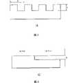
光源10输出短波长的激光束。作为该光源10,例如优选使用Q开关脉冲YAG激光(波长266nm)。光源10的激光平均输出例如为1W左右(脉冲循环:1kHz时)。脉冲宽度例如为1×10⁻⁹秒以上、1×10⁻⁷秒以下。另外,虽然在本实施方式中使用脉冲激光束,但本发明不限定于此,也可以使用CW(Continuous Wave)激光束。由光源10射出的激光束在通过快门11并被各反射镜12、13分别使进路(光路)改变90°后,向衍射光学元件14入射。快门11用于控制激光束的通过/遮断。The
衍射光学元件14将所入射的激光束分为多个激光束(衍射光束)。图2是衍射光学元件14的侧视图。如图2所示,衍射光学元件14具有使间隙为h(例如266nm)的两个水平(level)以周期p(例如0.50μm)设置的双(binary)结构,表面形状呈周期性构造。衍射光学元件14通过激光描绘和离子蚀刻被制作在石英基板上。另外,衍射光学元件14不限定于双结构,例如也可以构成表面形状呈正弦(余弦)曲面形状的周期性构造,或者,设计成外观平坦而内部的折射率周期性分布的周期性构造。The diffractive
第一透镜15将分支的多个衍射光束进行聚光并使其稳定化。在本实施方式中,第一透镜15的焦点距离f1例如为50mm。空间滤波器16仅使多个衍射光束中的两束衍射光束通过。The
相位差板17对通过了空间滤波器16的两束衍射光束的相互间赋予相位差。图3是相位差板1 7的侧视图。如图3所示,相位差板1 7在表面具有深度为g的阶梯差(间隙)。即,在图中右侧的区域和左侧的区域,相位差板17的厚度不同。由此,能够在通过了相位差板17的衍射光束和未通过相位差板17的衍射光束之间赋予规定的相位差(光路差)。本实施方式中,在相位差板17的板厚相对大的区域通过的衍射光束和未通过相位差板17的衍射光束之间的相位差φ被设定为0。另外,在相位差板17的板厚相对小的区域通过的衍射光束和未通过相位差板17的衍射光束之间的相位差φ被设定为π。相位差板17通过激光描绘和离子蚀刻被制作在石英基板上。此外,相位差板17不限定于厚度不同的带阶梯差的形状,例如,也可以是外观平坦、而左右区域的折射率不同的构成。另外,若相位差为π,则也可以使用1/2波长板作为相位差板17。The
第二透镜18对通过了相位差板17的两束衍射光束进行聚光。第二透镜18的焦点距离f2例如为28mm。由第二透镜18聚光后的两束衍射光束被照向对象物19。该两束衍射光束以规定的交叉角度θ进行干涉,产生周期性的干涉条纹(干涉光强度分布)。利用该干涉光强度分布,在对象物的表面形成了与干涉光强度分布对应的周期性的微细图案。基于衍射光束的曝光时间例如为数毫秒左右,该曝光时间由快门11进行控制。The
对于本实施方式的曝光装置1而言,所分叉的两束衍射光束相互接近,且干涉曝光所需要的时间短到数毫秒左右,因此,对于干扰极其稳定,不易受振动或空气起伏的影响。通常,激光干涉曝光系统对空气起伏较敏感,为了确保稳定性,需要将曝光系统配置在防振台上,并且,用坚固的罩对曝光系统和防振台进行覆盖等措施,从而在设备上需要花费高额成本,而根据本实施方式,能够通过简易的装置构成实现稳定的曝光系统。For the
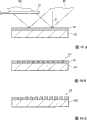
图4是概略地表示使两束衍射光束交叉而产生的干涉光照射到对象物上的样子的图。若将各衍射光束的波长设为λ,则使两束衍射光束以交叉角度θ交叉时而得到的干涉条纹F的周期P可用下式设定。FIG. 4 is a diagram schematically showing how interference light generated by intersecting two diffracted light beams is irradiated on an object. Assuming that the wavelength of each diffracted beam is λ, the period P of the interference fringe F obtained when two diffracted beams intersect at a crossing angle θ can be set by the following equation.
P=λ/(2sinθ) …(1)P=λ/(2sinθ) …(1)
此时,如图4所示,使两束衍射光束B1(第一激光束)、衍射光束B2(第二激光束)相对与对象物19的照射面正交的轴(假想轴)对称入射。由此,使干涉光的照射深度、宽度、或干涉条纹F的间距P等更加趋于均匀。At this time, as shown in FIG. 4 , two diffracted beams B1 (first laser beam) and diffracted beam B2 (second laser beam) are symmetrically incident on an axis (imaginary axis) perpendicular to the irradiation surface of the
图5是表示(1)式的关系的曲线图。横轴对应于交叉角度θ,纵轴对应于干涉条纹F的周期P。如图5所示,例如当波长λ为266nm、交叉角度θ为72度时,干涉条纹F的周期P为140nm。将含有这种窄间距的干涉条纹的干涉光向对象物19照射,由此,可以实现所期望的加工。其中,在本实施方式中,对象物19采用了具有热非线性特性的原材料。下面,对具有热非线性特性的原材料进行说明。Fig. 5 is a graph showing the relationship of the formula (1). The horizontal axis corresponds to the intersection angle θ, and the vertical axis corresponds to the period P of the interference fringe F. FIG. As shown in FIG. 5 , for example, when the wavelength λ is 266 nm and the crossing angle θ is 72 degrees, the period P of the interference fringes F is 140 nm. By irradiating the
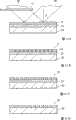
图6是对具有热非线性特性的原材料的一个例子进行说明的图。具体而言,图6表示了具有热非线性特性的原材料(例如氧化铂:PtO)的示差热分析的测定结果。如图所示,例如当对氧化铂进行加热时,在550℃附近显示出相位变化,氧化铂从非结晶状态(非变性状态)向结晶状态(变性状态)变化。将产生该相位变化的温度称作转移点Tc。在本实施方式中,将这样由于温度上升而引起陡峭(即,非线形)的相位变化的原材料称作“具有热非线性特性的原材料)。当将起因于这种相位变化的有无的非结晶区域及结晶区域混在一起的对象物19浸渍到碱水溶液中时,由于在这两个区域之间蚀刻速率存在差异,因此,例如结晶区域一方更早地被蚀刻。由此,能够产生与非结晶区域和结晶区域对应的凹凸。在本实施方式中,使用上述的干涉光对具有这种热非线性特性的原材料进行曝光。FIG. 6 is a diagram illustrating an example of a material having thermal nonlinear characteristics. Specifically, FIG. 6 shows the measurement results of differential thermal analysis of a material having thermal nonlinear properties (for example, platinum oxide: PtO). As shown in the figure, for example, when platinum oxide is heated, a phase change occurs at around 550° C., and platinum oxide changes from an amorphous state (non-denatured state) to a crystalline state (denatured state). The temperature at which this phase change occurs is called transition point Tc. In this embodiment, a material that causes a steep (that is, nonlinear) phase change due to an increase in temperature is referred to as "a material having thermal nonlinear characteristics). When the
图7是对具有热非线性特性的原材料的曝光进行概略表示的图。如图7所示,对形成于基板20上(例如玻璃基板上)的对象物19照射使两束衍射光束交叉而产生的干涉光。由此,在由具有热非线性特性的原材料构成的对象物19的表面,产生了与干涉光的干涉条纹F的周期P对应的周期性相位变化。即,在干涉光的强度相对高的区域,由具有热非线性特性的原材料构成的对象物19被加热而超过转移点Tc,由此产生相位转移,该区域变为结晶状态。另外,在干涉光的强度相对低的区域,由具有热非线性特性的原材料构成的对象物19因不怎么被加热而不会超过转移点Tc,由此,该区域不产生相位转移而保持原本的非结晶状态。如图8所示,产生相位变化的深度是距离对象物19的表面为dc的深度。直到该深度dc,对象物19的温度超过转移点Tc。考虑该情况,将对象物19的厚度设定在dc以下,以使在膜厚方向被完全加热到转移点Tc以上。在照射了干涉光之后,将对象物19放置于碱水溶液中时,具有和干涉条纹的周期P相等的周期的凹凸图案(深度=dc)显示在对象物19的表面。图9是概略地表示该样子的图。图示的例子表示了光强度相对弱而保持着非结晶状态的区域所残存的情况。另外,有时也保留光强度相对强而变为结晶状态的区域,该情况下,凹凸图案与光强度分布高的位置对应排列。如上述的图7所示,由于相位变化曲线的非线形性高,因此,通过适宜地控制激光束的照射条件,能够实现宽度窄、清晰的凹凸图案。FIG. 7 is a diagram schematically showing exposure of a material having thermal nonlinear characteristics. As shown in FIG. 7 , an
另外,具有热非线性特性的原材料除了上述的氧化铂膜以外,还可列举以下的无机材料。在本实施方式中,由于不需要使已经变为结晶状态的区域再次恢复为非结晶状态,因此,还可以使用不可逆变化型的原材料。例如:ZnS-SiO2、Ge-Sb-Te、Ge-Sb-Te-S、Te-TeO2-Ge-Sn、Te-Ge-Sn-Au、Ge-Te-Sn、Sn-Se-Te、Sb-Se-Te、Sb-Se、Ga-Se-Te-Ge、In-Se、In-Se-Tl-Co、Ge-Sb-Te、In-Se-Te、Ag-In-Sb-Te、TeO2-Pb等。能够采用它们中的任一种作为对象物19。In addition, as a material having thermal nonlinear characteristics, in addition to the above-mentioned platinum oxide film, the following inorganic materials can be exemplified. In the present embodiment, since it is not necessary to restore the region that has become crystalline to the amorphous state again, an irreversible change type raw material can also be used. For example: ZnS-SiO2 , Ge-Sb-Te, Ge-Sb-Te-S, Te-TeO2 -Ge-Sn, Te-Ge-Sn-Au, Ge-Te-Sn, Sn-Se-Te, Sb-Se-Te, Sb-Se, Ga-Se-Te-Ge, In-Se, In-Se-Tl-Co, Ge-Sb-Te, In-Se-Te, Ag-In-Sb-Te, TeO2 -Pb, etc. Any of them can be adopted as the
本实施方式的曝光装置1的构成及曝光原理(即光照射方法)如上所述,接着,对本实施方式所涉及的微细构造体的制造工序(制造方法)进行说明。The configuration and exposure principle (that is, the light irradiation method) of the
图10是表示本实施方式的微细构造体的制造工序的概略剖面图。使用如上所述的曝光装置1,通过使两束衍射光束以规定的交叉角度θ交叉而产生干涉光(第一光),将该干涉光对基板20上的对象物19进行照射(图10A)。此时,进行如上所述的设定,以使一方的衍射光束B2通过相位差板17,在其和另一方的衍射光束B1之间不产生相位差。另外,在图10中,为了方便对相位差板17进行图示,使相位差板17相对于衍射光束B2偏斜而进行了描绘,但如图1所示,实际上相位差板17以衍射光束B2与相位差板17的表面呈正交的方式配置。在以下说明的附图中也一样。FIG. 10 is a schematic cross-sectional view showing the manufacturing process of the microstructure of the present embodiment. Using the
以规定的交叉角度θ交叉的两束衍射光束B1、B2相互干涉,产生周期性的干涉条纹(干涉光强度分布)(参照图4)。通过被照射具有该干涉光强度分布的干涉光,使得对象物19在光强度高的区域引起相位转移,该区域(第一部分)21成为结晶状态(图10B)。该成为结晶状态的区域21(下面称作“结晶区域21。)的循环周期和干涉光强度分布的周期相等。干涉光的照射时间(曝光时间)例如为数毫秒左右,该照射时间(曝光时间)由快门11进行控制。The two diffracted beams B1 and B2 intersecting at a predetermined intersection angle θ interfere with each other to generate periodic interference fringes (interference light intensity distribution) (see FIG. 4 ). By being irradiated with interference light having this interference light intensity distribution, the
接着,通过将对象物19浸入到碱水溶液中来进行蚀刻。此时,在结晶区域21和其以外的区域(即,非结晶区域)之间产生了蚀刻速度差,例如结晶区域21比非结晶区域(第二部分)更早地被除掉。其结果是,形成了具有与干涉光的干涉条纹的周期对应的周期(本例中为140nm)的非结晶区域19’的图案(作为一例,为氧化铂图案)(图10C)。这种亚波长等级的微细构造体具有各种各样的用途。另外,在结晶区域21和非结晶区域19’之间产生的蚀刻速度的大小关系由原材料或由蚀刻溶液与原材料之间的关系来决定,有时非结晶区域比结晶区域21更早地被除掉。这种情况下,可得到结晶区域21的图案。Next, etching is performed by immersing the
这样,根据本实施方式,通过对具有热非线性特性的对象物照射具有干涉条纹的干涉光(第一光),可对应光强度相对高的区域和低的区域,得到变性区域(结晶区域)和非变性区域(非结晶区域)。这些变性区域和非变性区域的循环周期(间隔)可以通过减小交叉的两束激光束的波长、或增大交叉角度θ来缩短。通过采用具有热非线性特性的对象物,即使变性区域和非变性区域的循环周期小到100nm~200nm的程度,与现有的采用由有机材料构成的光致抗蚀剂膜的情况相比,也可以清晰地得到变性区域和非变性区域的边界。而且,由于在变性区域和非变性区域之间蚀刻速度产生差异,因此,通过对对象物进行蚀刻,可以形成分辨率高的微细构造体。Thus, according to this embodiment, by irradiating an object having thermal nonlinear characteristics with interference light (first light) having interference fringes, it is possible to obtain a denatured area (crystallized area) corresponding to a region with relatively high light intensity and a region with low light intensity. and non-denaturing regions (amorphous regions). The cycle period (interval) of these denatured regions and non-denatured regions can be shortened by reducing the wavelengths of the two laser beams crossing, or increasing the crossing angle θ. By using an object with thermal nonlinear characteristics, even if the cycle period between the denatured area and the non-denatured area is as small as 100nm to 200nm, compared with the conventional case of using a photoresist film composed of an organic material, The boundary between denatured and non-denatured areas can also be clearly obtained. Furthermore, since there is a difference in etching rate between the denatured region and the non-denatured region, a fine structure with high resolution can be formed by etching the object.
图11是表示微细构造体的制造工序的另一个实施方式的概略剖面图。在上述图10所示的实施方式中,考虑了利用通过蚀刻得到的非结晶区域19’的图案(作为一例为氧化铂图案)本身作为微细构造体的情况,也可以使用该非结晶区域19’的图案(或结晶区域21的图案)作为蚀刻掩模,将微细图案转印到另一对象物上。下面,对该情况进行说明。另外,对和上述的制造工序重复的内容的说明进行适当的简化。FIG. 11 is a schematic cross-sectional view showing another embodiment of the manufacturing process of the microstructure. In the above-mentioned embodiment shown in FIG. 10 , it is considered that the pattern (platinum oxide pattern as an example) itself of the amorphous region 19' obtained by etching is used as the fine structure, and the amorphous region 19' may also be used. The pattern (or the pattern of the crystalline region 21) is used as an etching mask to transfer the fine pattern to another object. Next, this case will be described. In addition, the description of the content overlapping with the above-mentioned manufacturing process is suitably simplified.
在本实施方式中,如图11A所示,预先在基板20的表面形成对象物22,然后在该对象物22的表面形成被膜19(作为一例,采用氧化铂膜)。其中,对象物22不特别限定于该内容,例如在本实施方式中可设定为铝或银等的金属膜。另外,基板20本身也可以是对象物。和上述同样地使两束衍射光束以交叉角度θ交叉而产生干涉光(第一光),并使该干涉光照射于对象物19。由此,和上述实施方式同样地可在被膜19上形成结晶区域21(图11B)。In this embodiment, as shown in FIG. 11A , an
接着,通过与上述实施方式同样地进行蚀刻,使得具有与干涉条纹的周期对应的周期的结晶区域21的图案(作为一例,是氧化铂图案)被除掉,保留被膜19中的非结晶区域19’的图案(图11C)。其后,将该非结晶区域19’的图案作为蚀刻掩模,进行对对象物22的蚀刻。此时的蚀刻的具体方法只要根据对象物22适宜地选择即可。作为一例,在本实施方式中进行干腐蚀。由此,非结晶区域19’的图案被转印到作为对象物22的铝膜上(图11D)。即,铝膜中的和非结晶区域19’(第二部分)未重叠的部分被除掉。这样一来,在基板20上形成了具有140nm周期的条纹状的铝膜23(铝格栅)。Next, by etching in the same manner as in the above-mentioned embodiment, the pattern of the
另外,在不形成对象物22,且经过了和上述图11A~图11C同样的工序的情况下,非结晶区域19’(或结晶区域21)的图案被转印到基板22的表面(未图示)。In addition, when the
这样,通过采用了具有热非线性特性的被膜,即使进一步减小结晶区域(变性区域)和非结晶区域(非变性区域)的循环周期(例如100nm~200nm程度),与采用现有的光致抗蚀剂膜等的情况相比,也可以清晰地得到结晶区域和非结晶区域的边界。而且,由于在结晶区域和非结晶区域之间蚀刻速度产生差异,因此,通过对被膜进行蚀刻,能够将结晶区域(或非结晶区域)除掉,使该区域开口。通过利用如此得到的具有开口的被膜作为蚀刻掩模,进行对于对象物的蚀刻,可以形成分辨率高的微细构造体。In this way, by using a film with thermal nonlinear characteristics, even if the cycle period (for example, about 100nm to 200nm) of the crystalline region (denatured region) and the amorphous region (non-denatured region) is further reduced, it is different from the existing photoinduced Compared with the case of a resist film or the like, the boundary between the crystalline region and the non-crystalline region can be clearly obtained. Furthermore, since there is a difference in etching rate between the crystalline region and the non-crystalline region, the crystalline region (or the non-crystalline region) can be removed by etching the film to open the region. By using the film having openings thus obtained as an etching mask to etch an object, a fine structure with high resolution can be formed.
图12是表示微细构造体的制造工序的又一个实施方式的概略剖面图。在通过上述图10或图11进行了说明的各实施方式中,进而如图12所示,将照射干涉光的工序进行两次以上,此时,优选在各工序都对两束衍射光束B1、B2相互间赋予相位差。Fig. 12 is a schematic cross-sectional view showing still another embodiment of the manufacturing process of the microstructure. In each of the embodiments described above with reference to FIG. 10 or FIG. 11 , as shown in FIG. 12 , the step of irradiating interference light is performed twice or more. B2 give phase difference to each other.
具体而言,在图12A所示的工序中,和上述各实施方式的情况同样地将两束衍射光束B1、B2相互间的相位差φ设定为φ0(任意值),使各衍射光束交叉,将由此产生的干涉光(第一光)向对象物19进行照射。将该φ=φ0的状态设定为基准状态(相位差为0的状态)。然后,在图12(B)所示的工序中,将两束衍射光束B1、B2相互间的相位差φ设定为φ0+π,使该各衍射光束交叉,将由此产生的干涉光(第二光)向对象物19进行照射。相位差的设定如上所述,通过相位差板17的配置变更来实现。当这样进行多重变更时,如图13所示,与第一次曝光形成的光强度分布(图中用实线表示)相对应,得到以周期P循环的结晶区域,进而在与通过第一次曝光而得到的结晶区域错开P/2的位置,与第二次曝光形成的光强度分布(图中用虚线表示)相对应,得到以周期P循环的结晶区域。若将它们作为整体来看,则得到了以周期P/2循环的结晶区域的图案。通过对这种状态的对象物19进行蚀刻,可得到周期为P/2的凹凸图案。如上所述(参照图6),由于对象物19对光的反应具有非线形特性,因此,在进行了第二次曝光后,也可以回避结晶区域的图案失去尖锐度(溃散),可得到窄间隔的图案。Specifically, in the process shown in FIG. 12A , the phase difference φ between the two diffracted beams B1 and B2 is set to φ0 (arbitrary value) as in the above-mentioned embodiments, and the diffracted beams are crossed. , and irradiates the
作为对本实施方式的比较,考虑到对象物对光的反应为线形的情况(例如,通常的光致抗蚀剂膜等),在基于与上述同样的窄间隔的干涉光多次进行曝光的情况下,图案将溃散。其原因在于光致抗蚀剂等与光反应的过程是单光子吸收。另外,在本实施方式中,对各衍射光束相互间的相位转移量设定为π,来形成波长的1/2周期的图案的情况进行了说明,但若将相位转移量设定为π/2,则能够以波长的1/4的周期形成图案,进而,若将相位转移量设定为π/4,则能够以波长的1/8的周期形成图案。As a comparison with the present embodiment, considering the case where the object responds to light in a linear manner (for example, a normal photoresist film, etc.), in the case of multiple exposures based on the interference light at narrow intervals similar to the above Next, the pattern will collapse. The reason for this is that the process of photoresist and the like reacting with light is single-photon absorption. In addition, in this embodiment, the case where the phase shift amount between the diffracted beams is set to π to form a pattern with a period of 1/2 of the wavelength has been described. However, if the phase shift amount is set to π/ 2, a pattern can be formed at a period of 1/4 of the wavelength, and further, if the phase shift amount is set to π/4, a pattern can be formed at a period of 1/8 of the wavelength.
这样,通过在两束激光束之间赋予相位差,能够使第一光的干涉条纹和第二光的干涉条纹以微小的宽度(例如1/2间距、1/4间距等)错开。使这样的第一光和第二光依次照射于具有热非线性特性的被膜,由此,能够进一步减小结晶区域(变性区域)和非结晶区域(非变性区域)的循环周期。这样,在循环周期进一步减小的情况下,由于使用了具有热非线性特性的被膜,因此,也可以清晰地得到结晶区域和非结晶区域的边界。从而,可得到分辨率更高的微细构造体。通过利用上述的热非线性特性和干涉光的相位转移,理论上可以脱离激光束的波长的制约而实现微细的图案。实际上,与现有技术相比,也可以实现特别微细的图案。Thus, by providing a phase difference between the two laser beams, the interference fringes of the first light and the interference fringes of the second light can be shifted by a small width (for example, 1/2 pitch, 1/4 pitch, etc.). By sequentially irradiating such a first light and a second light on the film having thermal nonlinear characteristics, the cycle period of the crystalline region (denatured region) and the amorphous region (non-denatured region) can be further reduced. In this way, when the cycle period is further reduced, the boundary between the crystallization region and the non-crystallization region can be clearly obtained due to the use of a coating having thermal nonlinear characteristics. Accordingly, a fine structure with higher resolution can be obtained. By utilizing the above-mentioned thermal nonlinear characteristics and phase shift of interfering light, it is theoretically possible to achieve a fine pattern without being restricted by the wavelength of the laser beam. In fact, particularly finer patterns can also be achieved compared to the prior art.
图14是表示微细构造体的制造工序的另一个实施方式的概略剖面图。在通过上述图10或图11进行了说明的各实施方式中,进而如图14所示,优选和照射干涉光的工序(激光干涉曝光工序)中的使用两束衍射光束而产生的干涉光同时,向对象物19(被膜)照射与该干涉光不同的光(第三光)。Fig. 14 is a schematic cross-sectional view showing another embodiment of the manufacturing process of the microstructure. In each of the embodiments described above with reference to FIG. 10 or FIG. 11 , as shown in FIG. 14 , it is preferable that the interference light generated using two diffracted light beams in the step of irradiating interference light (laser interference exposure step) be simultaneously Then, light (third light) different from the interference light is irradiated to the object 19 (film).
例如,向对象物19照射和干涉曝光所使用的衍射光束B1、B2不同的激光束B3。由此,相对于两束衍射光束B1、B2所产生的光照射强度,可得到由另一激光束B3给予偏置(byas)的作用。由此,如图15所示,对象物19上超过转移温度Tc的区域的深度dc进一步加深。这样一来,在对象物19上形成结晶区域,通过对其实施蚀刻,如图16所示,与通过上述图10或图11而说明的各实施方式的情况相比,可以在对象物19上形成更深的凹凸图案。另外,在作为对象物19而选择的材料的转移温度Tc高的情况下,也有利于向广泛的区域形成凹凸图案。而且,即使在用于产生干涉光的衍射光束B1、B2的输出小的情况下,通过进行上述的偏置曝光,也可以在对象物19表面的广泛区域形成凹凸图案。此外,在图示的例子中表示了保留光强度相对弱而维持非结晶状态的区域的情况,但有时也保留光强度相对强而变成结晶状态的区域。在这种情况下,凹凸图案对应光强度分布高的位置而排列。For example, the
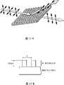
另外,通过进一步使用形成于该对象物19的凹凸图案作为蚀刻掩模,也可以将凹凸图案转印到事先设置在对象物19的背面侧的对象物(参照图11)上。In addition, by further using the concave-convex pattern formed on the
此外,第三光只要对于对象物19能够得到使温度偏置的作用即可,除了上述的激光束以外还可以使用各种光。就第三光的波长λ2而言,从给予有效的偏置这一观点出发,优选是和作为第一光的各衍射光束B1、B2的波长λ1相同或接近的值,但不限于此。并且,第三光不一定非要是单波长的光(单色光),也可以是含有多种波长成分的光。作为产生第三光的光源,例如可以使用受激准分子激光器(波长308nm)。通过并用这种偏置曝光,可以扩大能够由干涉光曝光的区域,从而,可向更广的区域同时形成图案。In addition, as long as the third light can obtain the action of biasing the temperature of the
下面,对应用上述的实施方式来制造金属格栅型偏光分离元件时的一个具体例(实施例)进行说明。Next, a specific example (example) when the above-mentioned embodiment is applied to manufacture a metal grid type polarization splitting element will be described.
在石英玻璃基板上形成铝膜,进而在该铝膜上形成氧化铂膜。对于各自的膜厚而言,例如铝膜为150nm,氧化铂膜为100nm。使用Q开关纳米秒脉冲YAG激光(波长266nm)作为光源10。激光平均输出为1W(脉冲循环频率:1kHz时)。将自该光源10射出的激光束分为两束,通过使该分支后的两束激光束(衍射光束)交叉而产生干涉光。干涉角度θ为72度。根据上述的式(1),作为对象物的氧化铂膜的表面的干涉条纹的周期为140nm。使用该干涉光进行一次曝光。另外,也可以适当地并用使用了第三光的偏置曝光。其后,使用碱水溶液进行蚀刻,由此,其结果是,形成了具有和干涉条纹的周期同周期,即140nm周期的氧化铂图案。进而,使用该氧化铂图案作为蚀刻掩模对铝膜进行干腐蚀,由此将氧化铂图案向其下面的铝膜进行转印。这样一来,在石英玻璃基板上形成了具有140nm周期的条纹状的铝膜(铝格栅)。这种微细构造体例如可以用作偏光分离元件。An aluminum film is formed on a quartz glass substrate, and a platinum oxide film is further formed on the aluminum film. The respective film thicknesses are, for example, 150 nm for the aluminum film and 100 nm for the platinum oxide film. A Q-switched nanosecond pulsed YAG laser (wavelength 266 nm) was used as the
另外,在以上述的条件产生干涉光时,第一次各光束相互间的相位差φ=φ0(任意值),第二次相位差φ=φ0+π。即,第一次和第二次的相位差设定为π。如此来进行第二次曝光。另外,也可以适当地并用使用了第三光的偏置曝光。其后,使用碱水溶液进行蚀刻,由此,形成具有干涉条纹的周期的二分之一,即70nm周期的氧化铂图案。进而,使用该氧化铂图案作为蚀刻掩模对铝膜进行干腐蚀,由此将氧化铂图案向其下面的铝膜进行转印。这样一来,可在石英玻璃基板上形成具有70nm周期的条纹状的铝膜(铝格栅)。这种微细构造体例如可以用作偏光分离元件。In addition, when interfering light is generated under the above-mentioned conditions, the phase difference between the beams is φ=φ0 (arbitrary value) in the first phase, and the phase difference φ=φ0+π in the second phase. That is, the phase difference between the first time and the second time is set to π. Do this for the second exposure. In addition, bias exposure using the third light may be used in combination as appropriate. Thereafter, by etching using an aqueous alkali solution, a platinum oxide pattern having a period of 1/2 the period of the interference fringes, that is, 70 nm, was formed. Furthermore, the aluminum film was dry-etched using this platinum oxide pattern as an etching mask, whereby the platinum oxide pattern was transferred to the aluminum film below it. In this way, a striped aluminum film (aluminum grid) having a period of 70 nm can be formed on the quartz glass substrate. Such a microstructure can be used, for example, as a polarization separation element.
图17是示意性地表示如上所述而制造的偏光分离元件的构造的图。具体而言,图17A是概略表示偏光分离元件的功能的立体图,图17B是该偏光分离元件的局部概略剖面图。该偏光分离元件在玻璃基板(SiO2)上以条纹状(一维栅格图案)形成有厚度150nm的铝膜。铝膜的栅格的周期P为70nm或140nm。玻璃基板的复介电常数N=1.5-j0.0,铝膜的复介电常数N=0.59-j5.34。图18表示了这种偏光分离元件的偏光分离特性。在图18中,纵轴为透光率(左侧)和对比度(右侧),横轴为栅格周期P和波长λ的比。对比度以TE偏光的透光率和TM偏光的透光率之比来定义。由该结果可知,构成偏光分离元件的栅格图案(亚波长构造)的周期P越短,作为偏光分离元件的性能越高(即透光率高,对比度高)。在图18中,与周期P=70nm相对的特性及与周期P=140nm相对的特性分别用箭头表示于图表上部。在任一偏光分离元件中都可得到优良的偏光分离特性。可知尤其是周期P=70nm的偏光分离元件的特性与周期P=140nm的偏光分离元件相比,透过率以及对比度都特别优异。FIG. 17 is a diagram schematically showing the structure of the polarized light separation element manufactured as described above. Specifically, FIG. 17A is a perspective view schematically showing the function of the polarization separation element, and FIG. 17B is a partial schematic cross-sectional view of the polarization separation element. In this polarized light separation element, an aluminum film having a thickness of 150 nm was formed in stripes (one-dimensional grid pattern) on a glass substrate (SiO2 ). The period P of the grid of the aluminum film is 70 nm or 140 nm. The complex dielectric constant of the glass substrate is N=1.5-j0.0, and the complex dielectric constant of the aluminum film is N=0.59-j5.34. FIG. 18 shows the polarization separation characteristics of this polarization separation element. In FIG. 18 , the vertical axis represents light transmittance (left side) and contrast ratio (right side), and the horizontal axis represents the ratio of grating period P to wavelength λ. Contrast is defined by the ratio of the transmittance of TE polarized light to the transmittance of TM polarized light. From this result, it can be seen that the shorter the period P of the grid pattern (sub-wavelength structure) constituting the polarization separation element, the higher the performance (that is, high light transmittance and high contrast) as the polarization separation element. In FIG. 18, the characteristics corresponding to the period P=70 nm and the characteristics corresponding to the period P=140 nm are indicated by arrows in the upper part of the graph, respectively. Excellent polarization separation characteristics can be obtained in any of the polarization separation elements. In particular, it can be seen that the characteristics of the polarized light separation element with a period P=70 nm are particularly excellent in transmittance and contrast compared with the polarized light separation element with a period P=140 nm.
另外,本发明不限定于上述的实施方式的内容,可以在本发明的主旨范围内实施各种变形。在上述的实施方式中,作为应用了本发明的具体例,列举了偏光分离元件,但除此以外,本发明在微细构造图案的形成所必需的各种器件的制造中都是有用的。作为器件可列举:光学薄膜器件、半导体薄膜器件、标记(marking)、微小机械零件等。作为对光学薄膜器件的应用,例如可举出:液晶应用设备所使用的反射防止膜、相位差板、光波导路径、偏光元件、取向膜、LED元件、EL元件等发光元件所用的光子能带结构、高密度光盘等。In addition, this invention is not limited to the content of the said embodiment, Various deformation|transformation is possible within the scope of this invention. In the above-mentioned embodiments, the polarized light separation element was cited as a specific example to which the present invention is applied, but the present invention is also useful in the manufacture of various devices necessary for the formation of fine structure patterns. Examples of the device include optical thin film devices, semiconductor thin film devices, marking, and micromechanical parts. Applications to optical thin-film devices include, for example, anti-reflection films used in liquid crystal applications, retardation plates, optical waveguides, polarizing elements, alignment films, LED elements, and photonic energy bands used in light-emitting elements such as EL elements. structures, high-density discs, etc.
另外,在上述的实施方式中,作为变性区域的一例列举了结晶状态,作为非变性区域的一例列举了非结晶状态,但变性区域及非变性区域不限于此。变性区域及非变性区域只要是能够因两者的物性(物理或化学特性)不同而产生蚀刻速度的差即可。In addition, in the above-mentioned embodiment, the crystalline state was cited as an example of the denatured region, and the amorphous state was cited as an example of the non-denatured region, but the denatured region and the non-denatured region are not limited thereto. The denatured region and the non-denatured region may be any difference in etching rate due to the difference in physical properties (physical or chemical properties) between the two.
Claims (14)
Applications Claiming Priority (2)
| Application Number | Priority Date | Filing Date | Title |
|---|---|---|---|
| JP2007039870AJP4269295B2 (en) | 2007-02-20 | 2007-02-20 | Manufacturing method of fine structure |
| JP2007039870 | 2007-02-20 |
Publications (1)
| Publication Number | Publication Date |
|---|---|
| CN101251617Atrue CN101251617A (en) | 2008-08-27 |
Family
ID=39781126
Family Applications (1)
| Application Number | Title | Priority Date | Filing Date |
|---|---|---|---|
| CN200810080736.9APendingCN101251617A (en) | 2007-02-20 | 2008-02-18 | Method for producing microstructures |
Country Status (3)
| Country | Link |
|---|---|
| US (1) | US8529782B1 (en) |
| JP (1) | JP4269295B2 (en) |
| CN (1) | CN101251617A (en) |
Cited By (8)
| Publication number | Priority date | Publication date | Assignee | Title |
|---|---|---|---|---|
| CN102072879A (en)* | 2009-11-19 | 2011-05-25 | 精工爱普生株式会社 | Sensor chip, sensor cartridge and analysis device |
| CN103018210A (en)* | 2009-11-19 | 2013-04-03 | 精工爱普生株式会社 | Sensor chip, sensor cartridge, and analysis apparatus |
| CN103809376A (en)* | 2014-02-20 | 2014-05-21 | 苏州华维纳纳米科技有限公司 | Inorganic phase change photoresist and photolithographic technology based on inorganic phase change photoresist |
| CN110100200A (en)* | 2016-12-22 | 2019-08-06 | 奇跃公司 | Color separation in a waveguide using a dichroic filter |
| CN111002115A (en)* | 2020-01-16 | 2020-04-14 | 程凯芬 | Anti-glare glass and processing method thereof |
| CN111045227A (en)* | 2019-08-29 | 2020-04-21 | 中山大学 | A kind of chalcogenide phase change material with transparent communication band and preparation method thereof |
| CN111295602A (en)* | 2017-11-02 | 2020-06-16 | 国立研究开发法人产业技术综合研究所 | Method for producing light absorber |
| CN114008540A (en)* | 2019-07-15 | 2022-02-01 | Asml荷兰有限公司 | Methods of aligning, overlapping, configuring marks, making patterning devices and patterning marks |
Families Citing this family (3)
| Publication number | Priority date | Publication date | Assignee | Title |
|---|---|---|---|---|
| KR101224326B1 (en) | 2009-11-19 | 2013-01-21 | 세이코 엡슨 가부시키가이샤 | Sensor chip, sensor cartridge, and analysis apparatus |
| JP5845597B2 (en)* | 2011-03-10 | 2016-01-20 | ダイキン工業株式会社 | Manufacturing method of fine structure |
| JP6790731B2 (en)* | 2016-11-01 | 2020-11-25 | 東洋製罐グループホールディングス株式会社 | Method of forming microperiodic structure grooves on the surface of diamond film |
Family Cites Families (17)
| Publication number | Priority date | Publication date | Assignee | Title |
|---|---|---|---|---|
| JPS569706B2 (en) | 1972-09-07 | 1981-03-03 | ||
| US4490211A (en)* | 1984-01-24 | 1984-12-25 | International Business Machines Corporation | Laser induced chemical etching of metals with excimer lasers |
| JPS62255985A (en) | 1986-04-28 | 1987-11-07 | Fujitsu Ltd | Forming method for hologram |
| JPH1097738A (en) | 1996-09-20 | 1998-04-14 | Matsushita Electric Ind Co Ltd | Method and apparatus for manufacturing optical information recording medium |
| JP4232253B2 (en) | 1999-01-27 | 2009-03-04 | パナソニック株式会社 | Fine pattern manufacturing apparatus and holographic memory recording / reproducing apparatus |
| JP2002251786A (en)* | 2001-02-22 | 2002-09-06 | Sony Corp | Optical recording medium and its manufacture |
| EP1426940B1 (en)* | 2001-09-12 | 2008-05-14 | Matsushita Electric Industrial Co., Ltd. | Optical information recording medium and recording method using it |
| US20040246884A1 (en)* | 2001-09-13 | 2004-12-09 | Tsuyoshi Komaki | Optical recording medium manufacturing method |
| JP2004103208A (en)* | 2002-07-18 | 2004-04-02 | Nec Corp | Information recording medium, method for indicator generation, manufacturing method, recording condition adjusting method, and recording method for the same medium, and information recorder |
| EP1571659B1 (en)* | 2002-10-30 | 2012-08-01 | TDK Corporation | Method for evaluating optical information medium and optical information medium |
| US6841883B1 (en)* | 2003-03-31 | 2005-01-11 | Micron Technology, Inc. | Multi-dice chip scale semiconductor components and wafer level methods of fabrication |
| JP2004348830A (en)* | 2003-05-21 | 2004-12-09 | Samsung Electronics Co Ltd | Multilayer structure for drawing fine structure, drawing method, method for producing master of optical disk using the same, and method for mastering |
| EP1513144A2 (en)* | 2003-08-26 | 2005-03-09 | Matsushita Electric Industrial Co., Ltd. | Method for producing a master disk of a recording medium, method for producing a stamper, method for producing a recording medium, master disk of a recording medium, stamper of a recording medium, and recording medium |
| JP4389791B2 (en) | 2004-08-25 | 2009-12-24 | セイコーエプソン株式会社 | Fine structure manufacturing method and exposure apparatus |
| CN100480863C (en) | 2004-08-25 | 2009-04-22 | 精工爱普生株式会社 | Method for manufacturing a microstructure, exposure device, and electronic apparatus |
| JP4780602B2 (en) | 2005-02-10 | 2011-09-28 | ブラザー工業株式会社 | Manufacturing method of ultra fine wiring board |
| JP2006339359A (en) | 2005-06-01 | 2006-12-14 | Seiko Epson Corp | Microstructure manufacturing method, electronic device |
- 2007
- 2007-02-20JPJP2007039870Apatent/JP4269295B2/ennot_activeExpired - Fee Related
- 2008
- 2008-02-18CNCN200810080736.9Apatent/CN101251617A/enactivePending
- 2008-02-19USUS12/033,430patent/US8529782B1/ennot_activeExpired - Fee Related
Cited By (12)
| Publication number | Priority date | Publication date | Assignee | Title |
|---|---|---|---|---|
| CN102072879A (en)* | 2009-11-19 | 2011-05-25 | 精工爱普生株式会社 | Sensor chip, sensor cartridge and analysis device |
| CN102072879B (en)* | 2009-11-19 | 2013-01-02 | 精工爱普生株式会社 | Sensor chip, sensor cartridge and analysis device |
| CN103018210A (en)* | 2009-11-19 | 2013-04-03 | 精工爱普生株式会社 | Sensor chip, sensor cartridge, and analysis apparatus |
| CN103018210B (en)* | 2009-11-19 | 2015-06-17 | 精工爱普生株式会社 | Analysis apparatus |
| CN103809376A (en)* | 2014-02-20 | 2014-05-21 | 苏州华维纳纳米科技有限公司 | Inorganic phase change photoresist and photolithographic technology based on inorganic phase change photoresist |
| CN110100200A (en)* | 2016-12-22 | 2019-08-06 | 奇跃公司 | Color separation in a waveguide using a dichroic filter |
| CN111295602A (en)* | 2017-11-02 | 2020-06-16 | 国立研究开发法人产业技术综合研究所 | Method for producing light absorber |
| CN111295602B (en)* | 2017-11-02 | 2022-03-29 | 国立研究开发法人产业技术综合研究所 | Method for producing light absorber |
| CN114008540A (en)* | 2019-07-15 | 2022-02-01 | Asml荷兰有限公司 | Methods of aligning, overlapping, configuring marks, making patterning devices and patterning marks |
| CN114008540B (en)* | 2019-07-15 | 2024-12-17 | Asml荷兰有限公司 | Alignment, overlay, configuration of marks, method of manufacturing a patterning device and patterning marks |
| CN111045227A (en)* | 2019-08-29 | 2020-04-21 | 中山大学 | A kind of chalcogenide phase change material with transparent communication band and preparation method thereof |
| CN111002115A (en)* | 2020-01-16 | 2020-04-14 | 程凯芬 | Anti-glare glass and processing method thereof |
Also Published As
| Publication number | Publication date |
|---|---|
| US20130248489A1 (en) | 2013-09-26 |
| JP4269295B2 (en) | 2009-05-27 |
| JP2008203553A (en) | 2008-09-04 |
| US8529782B1 (en) | 2013-09-10 |
Similar Documents
| Publication | Publication Date | Title |
|---|---|---|
| CN101251617A (en) | Method for producing microstructures | |
| Rekstyte et al. | Nanoscale precision of 3D polymerisation via polarisation control | |
| Choi et al. | Formation of cylindrical micro-lens array on fused silica glass surface using CO2 laser assisted reshaping technique | |
| JP2007057622A (en) | Optical element and manufacturing method thereof, manufacturing method of shape transfer mold for optical element, and transfer mold for optical element | |
| JP2005014059A (en) | Ultrashort pulse laser processing method, processing apparatus and structure | |
| JP2005262290A (en) | Laser processing apparatus, laser processing method, and structure manufactured by the processing apparatus or processing method | |
| JP2022523765A (en) | Optical metasurfaces, related manufacturing methods and systems | |
| Geng et al. | Quasicylindrical waves for ordered nanostructuring | |
| US10101652B2 (en) | Exposure method, method of fabricating periodic microstructure, method of fabricating grid polarizing element and exposure apparatus | |
| JP6221849B2 (en) | Exposure method, method for manufacturing fine periodic structure, method for manufacturing grid polarizing element, and exposure apparatus | |
| Mazloumi et al. | Hierarchical concentric surface patterns and metasurfaces on azobenzene molecular glass films using axicon interference lithography | |
| KR101753355B1 (en) | Laser holographic lithography device and method of manufacturing for pattern | |
| Qian et al. | Tunable filter with varied-line-spacing grating fabricated using holographic recording | |
| Molotokaite et al. | Picosecond laser beam interference ablation of thin metal films on glass substrate | |
| KR20220148321A (en) | A method for producing a continuously diffractive optical element, an apparatus for performing the production method, and a continuously diffractive optical element | |
| JP4436162B2 (en) | Laser processing equipment | |
| Choi et al. | Formation of cylindrical micro-lens array in fused silica glass using laser irradiations | |
| Takayuki et al. | Fabrication of Dammann Gratings Inside Glasses by aFemtosecond Laser | |
| Kondo et al. | Three-dimensional recording by femtosecond pulses in polymer materials | |
| Song et al. | Multi-functional dual-path self-aligned polarization interference lithography | |
| Jia et al. | Manipulation of cross-linked micro/nanopatterns on ZnO by adjusting the femtosecond-laser polarizations of four-beam interference | |
| JP2006339359A (en) | Microstructure manufacturing method, electronic device | |
| CN1168981A (en) | A method for fabricating a grating on the surface of an ultraviolet absorbing material and its product | |
| Lasagni et al. | Fabrication of periodic submicrometer and micrometer arrays using laser interference-based methods | |
| CN108681216A (en) | A kind of device and method for the micron and nanometer composite structure preparing multicycle multiform looks |
Legal Events
| Date | Code | Title | Description |
|---|---|---|---|
| C06 | Publication | ||
| PB01 | Publication | ||
| C10 | Entry into substantive examination | ||
| SE01 | Entry into force of request for substantive examination | ||
| C12 | Rejection of a patent application after its publication | ||
| RJ01 | Rejection of invention patent application after publication | Open date:20080827 |