CN101244533B - Method of ultra-flat chemical mechanical polishing technique and semiconductor device manufactured using the same - Google Patents
Method of ultra-flat chemical mechanical polishing technique and semiconductor device manufactured using the sameDownload PDFInfo
- Publication number
- CN101244533B CN101244533BCN2007100802816ACN200710080281ACN101244533BCN 101244533 BCN101244533 BCN 101244533BCN 2007100802816 ACN2007100802816 ACN 2007100802816ACN 200710080281 ACN200710080281 ACN 200710080281ACN 101244533 BCN101244533 BCN 101244533B
- Authority
- CN
- China
- Prior art keywords
- layer
- etching
- ground floor
- grooves
- forming
- Prior art date
- Legal status (The legal status is an assumption and is not a legal conclusion. Google has not performed a legal analysis and makes no representation as to the accuracy of the status listed.)
- Active
Links
Images


Classifications
- H—ELECTRICITY
- H10—SEMICONDUCTOR DEVICES; ELECTRIC SOLID-STATE DEVICES NOT OTHERWISE PROVIDED FOR
- H10H—INORGANIC LIGHT-EMITTING SEMICONDUCTOR DEVICES HAVING POTENTIAL BARRIERS
- H10H20/00—Individual inorganic light-emitting semiconductor devices having potential barriers, e.g. light-emitting diodes [LED]
- H10H20/01—Manufacture or treatment
- H10H20/011—Manufacture or treatment of bodies, e.g. forming semiconductor layers
- H10H20/018—Bonding of wafers
- H—ELECTRICITY
- H10—SEMICONDUCTOR DEVICES; ELECTRIC SOLID-STATE DEVICES NOT OTHERWISE PROVIDED FOR
- H10H—INORGANIC LIGHT-EMITTING SEMICONDUCTOR DEVICES HAVING POTENTIAL BARRIERS
- H10H20/00—Individual inorganic light-emitting semiconductor devices having potential barriers, e.g. light-emitting diodes [LED]
- H10H20/80—Constructional details
- H10H20/81—Bodies
- H10H20/819—Bodies characterised by their shape, e.g. curved or truncated substrates
- H10H20/82—Roughened surfaces, e.g. at the interface between epitaxial layers
- H—ELECTRICITY
- H10—SEMICONDUCTOR DEVICES; ELECTRIC SOLID-STATE DEVICES NOT OTHERWISE PROVIDED FOR
- H10H—INORGANIC LIGHT-EMITTING SEMICONDUCTOR DEVICES HAVING POTENTIAL BARRIERS
- H10H20/00—Individual inorganic light-emitting semiconductor devices having potential barriers, e.g. light-emitting diodes [LED]
- H10H20/80—Constructional details
- H10H20/872—Periodic patterns for optical field-shaping, e.g. photonic bandgap structures
Landscapes
- Led Devices (AREA)
Abstract
Translated fromChinese
Description
Translated fromChinese技术领域technical field
本发明一般地涉及半导体领域,在半导体之制作过程中涉及使用化学机械抛光技术来制作平坦表面之方法,其主要是一种在半导体之制作过程中用以取代激光剥离(laser lift-off)之方法。The present invention generally relates to the field of semiconductors, and relates to a method of using chemical mechanical polishing technology to make a flat surface in the manufacturing process of semiconductors. It is mainly a method for replacing laser lift-off (laser lift-off) in the manufacturing process of semiconductors. method.
背景技术Background technique
传统用于制造一覆晶发光二极管组件之方法中,沉积多个磊晶层于一蓝宝石成长基板上以产生一磊芯片。在该磊芯片上制造复数个发光二极管组件。切割该磊芯片以产生一组件晶粒。覆晶接合该组件晶粒至一安装台。该覆晶接合包括藉由接合该组件晶粒之至少一电极至该安装台之至少一焊垫来固定该组件晶粒于该安装台上。继该覆晶接合之后,经由应用激光来移除该组件晶粒之该成长基板。In the conventional method for manufacturing a flip-chip LED device, multiple epitaxial layers are deposited on a sapphire growth substrate to produce an epitaxial chip. A plurality of LED components are manufactured on the epitaxial chip. The epichip is diced to produce a component die. Flip chip bonding the component die to a mount. The flip-chip bonding includes fixing the component die on the mounting platform by bonding at least one electrode of the component chip to at least one bonding pad of the mounting platform. Following the flip chip bonding, the growth substrate of the device die is removed by applying a laser.
目前出现一种取代覆晶发光二极管组件之薄膜发光二极管组件,与覆晶发光二极管组件相比薄膜氮化镓(GaN)发光二极管组件具有低热阻、在N型层与P型层具有均匀电流以及低成本之优点。薄膜发光二极管组件直接将磊芯片黏接至一电导性载体基板。接着使用准分子激光(excimer laser)分解氮化镓,藉此移除蓝宝石基板而只保留活性区。At present, there is a thin-film light-emitting diode component that replaces flip-chip light-emitting diode components. Compared with flip-chip light-emitting diode components, thin-film gallium nitride (GaN) light-emitting diode components have low thermal resistance, uniform current flow in the N-type layer and P-type layer, and The advantage of low cost. Thin film light emitting diode components directly bond epitaxial chips to a conductive carrier substrate. An excimer laser is then used to decompose the GaN, thereby removing the sapphire substrate and leaving only the active area.
上述移除蓝宝石基板之方法称为激光剥离(laser lift-off),该方法在美国专利6455340、7001824以及7015117被揭露。目前激光剥离是唯一实现薄膜氮化镓(GaN)发光二极管组件之方法,但是激光剥离不兼容于旧制程,所以具有设备昂贵以及激光会产生损害之缺点。The above method of removing the sapphire substrate is called laser lift-off, which is disclosed in US Patents 6,455,340, 7,001,824 and 7,015,117. At present, laser lift-off is the only method to realize thin-film gallium nitride (GaN) light-emitting diode components, but laser lift-off is not compatible with the old process, so it has the disadvantages of expensive equipment and laser damage.
若是使用传统之化学机械抛光技术(CMP)取代激光剥离(laser lift-off),该技术相较于激光剥离,因不需增加激光设备以及使用激光剥离技术而达到降低成本以及实施方便之优点。不过由于实施传统之化学机械抛光技术时,若欲抛光之平面过大,将造成平面两侧与中心位置之变异值过大,无法达到大量制造半导体装置时要求平面必须平坦之标准,将使得制造半导体装置之良率降低。于是本发明提供一种超平坦化学机械抛光技术(Super Flat Chemical Mechanical Polishing(SF-CMP))之方法,该方法克服了传统之化学机械抛光技术(CMP)之平面两侧与中心位置之变异值过大之缺点,所以同时具有降低成本、实施方便以及提高良率之优点。If traditional chemical mechanical polishing (CMP) is used to replace laser lift-off, compared with laser lift-off, this technology has the advantages of lower cost and convenient implementation because it does not need to add laser equipment and use laser lift-off technology. However, due to the implementation of traditional chemical mechanical polishing technology, if the plane to be polished is too large, the variation value between the two sides of the plane and the center position will be too large, which cannot meet the standard that the plane must be flat when manufacturing semiconductor devices in large quantities. The yield rate of semiconductor devices decreases. Therefore, the present invention provides a method of Super Flat Chemical Mechanical Polishing (SF-CMP), which overcomes the variation value between the two sides and the central position of the plane of the traditional chemical mechanical polishing (CMP) It has the disadvantage of being too large, so it has the advantages of reducing cost, facilitating implementation and improving yield.
发明内容Contents of the invention
本发明在于提供一种超平坦化学机械抛光技术(Super FlatChemical Mechanical Polishing(SF-CMP))之方法,其主要步骤是在想要抛光的表面上,先植入复数个抛光停止点后再进行抛光。其特征在于该等抛光停止点的材料之硬度大于该表面的材料之硬度。此方法可以在不需移除抛光停止点的情形下获得超平坦的抛光表面。该方法包含以下步骤:(a)提供一第一物质,用于形成一第一层;(b)提供一第二物质,用于在该第一层之一面上形成一第二层;(c)蚀刻该第二层,用于产生复数个露出该第一层的表面之沟槽;(d)填充一硬度大于该第一物质及该第二物质之第三物质于该等沟槽中形成复数个抛光停止点;以及(e)移除该等沟槽外之该第三物质,而暴露出该第二层之表面;(f)把第二层之表面粘附于一导电之第四物质上;以及(g)用机械或化学机械方法磨除第一物质暴露出第二层物质。其中蚀刻之步骤是感应耦合电浆、该第三物质是钻石薄膜或类金刚石薄膜以及移除是使用机械研磨或化学机械抛光。The present invention is to provide a method of Super Flat Chemical Mechanical Polishing (SF-CMP), the main step of which is to implant a plurality of polishing stop points on the surface to be polished before polishing . It is characterized in that the hardness of the material of the polishing stops is greater than the hardness of the material of the surface. This method can achieve an ultra-flat polished surface without removing polishing stops. The method comprises the steps of: (a) providing a first substance for forming a first layer; (b) providing a second substance for forming a second layer on one side of the first layer; (c ) Etching the second layer to produce a plurality of grooves exposing the surface of the first layer; (d) filling a third substance with a hardness greater than that of the first substance and the second substance in the grooves a plurality of polishing stops; and (e) remove the third material outside the trenches to expose the surface of the second layer; (f) adhere the surface of the second layer to a conductive fourth on the substance; and (g) mechanically or chemomechanically abrading the first substance to expose the second layer of substance. The etching step is inductively coupled plasma, the third substance is a diamond film or a diamond-like film, and the removal is performed by mechanical grinding or chemical mechanical polishing.
本发明也提供一种制作薄膜发光二极管组件之方法,该方法包含以下步骤:一种制造半导体发光装置之方法,该方法包含以下步骤:(a)提供一第一物质,用于形成一第一层;(b)提供一半导体材料之第二物质,用于在该第一层之一面上形成一做为活性区(active region)之第二层;(c)蚀刻该第二层,用于产生复数个露出该第一层的表面之沟槽;(d)覆盖一层介质;(e)填充一硬度大于该第一物质及该第二物质之第三物质于该等沟槽中形成复数个抛光停止点;(f)提供一第四物质,用于在该第二层之表面上形成一第一电极层;(g)黏接该第一电极层至一电导式载体上;(h)移除该第一层;以及(i)在移除该第一层后之该第二物质之表面上形成复数个第二电极。其中该第一物质为蓝宝石、该第二物质为氮化镓或氮化铟镓或III-V族或II-VI之半导体材料、该第三物质是钻石薄膜或类金刚石薄膜、(c)步骤中之蚀刻是感应耦合电浆蚀刻、(h)步骤中之移除是使用机械研磨或化学机械抛光、该第一电极层是P型以及该第二电极层是N型。上述方法进一步包含在抛光后之表面上进行表皮粗糙化的步骤或形成2维光子晶体的步骤。The present invention also provides a method for manufacturing a thin-film light-emitting diode assembly, the method comprising the following steps: a method for manufacturing a semiconductor light-emitting device, the method comprising the following steps: (a) providing a first substance for forming a first layer; (b) providing a second substance of a semiconductor material for forming a second layer as an active region (active region) on one side of the first layer; (c) etching the second layer for Produce a plurality of grooves that expose the surface of the first layer; (d) cover a layer of medium; (e) fill a third material with a hardness greater than that of the first material and the second material to form multiple grooves in the grooves (f) providing a fourth substance for forming a first electrode layer on the surface of the second layer; (g) bonding the first electrode layer to an electroconductive carrier; (h ) removing the first layer; and (i) forming a plurality of second electrodes on the surface of the second substance after removing the first layer. Wherein the first substance is sapphire, the second substance is gallium nitride or indium gallium nitride or III-V group or II-VI semiconductor material, the third substance is a diamond film or a diamond-like film, (c) step The etching is inductively coupled plasma etching, the removal in step (h) is using mechanical grinding or chemical mechanical polishing, the first electrode layer is P-type and the second electrode layer is N-type. The above method further comprises a step of roughening the surface or forming a 2D photonic crystal on the polished surface.
由于本发明之一实施例是在发光二极管之活性区(activeregion)植入钻石材料,以做为复数个抛光停止点。于是本发明称其为一种钻石肩(diamond shoulder)发光二极管结构。One embodiment of the present invention is to implant diamond material in the active region of the LED as a plurality of polishing stop points. Therefore, the present invention calls it a diamond shoulder light emitting diode structure.
在本发明之一实施例中是专注在移除薄膜装置之基板,而且使用钻石膜在发光装置中的好处是可以帮助热耗散。且在本发明之之一实施例中,在活性区的周围植入钻石膜以防止活性区在移除活性区之顶层材料或底层材料之步骤中被移除掉。更细部而言,在一制作薄膜发光二极管组件之一实施例中,所有半导体制程之步骤是有关制作薄膜发光二极管组件,而抛光停止点是用于移除蓝宝石层之辅助方法。One embodiment of the present invention is focused on removing the substrate of thin-film devices, and the benefit of using diamond film in light-emitting devices is that it can help heat dissipation. And in one embodiment of the present invention, a diamond film is implanted around the active area to prevent the active area from being removed during the step of removing top or bottom material of the active area. In more detail, in one embodiment of fabricating a thin film LED device, all semiconductor process steps are related to fabricating a thin film LED device, and the polishing stop is an auxiliary method for removing the sapphire layer.
附图说明Description of drawings
图1描绘了实施传统化学机械抛光技术后之平面。Figure 1 depicts the plane after performing conventional chemical mechanical polishing techniques.
图2描绘了实施超平坦化学机械抛光技术后之平面。Figure 2 depicts the planar surface after implementing the ultra-flat chemical mechanical polishing technique.
图3描绘了根据本发明一实施例应用之停止点分布图之剖面图。Figure 3 depicts a cross-sectional view of a stop point profile applied in accordance with one embodiment of the present invention.
图4描绘了根据本发明一实施例应用之初始样本之剖面图。Figure 4 depicts a cross-sectional view of an initial sample used in accordance with an embodiment of the present invention.
图5描绘了根据本发明一实施例应用之蚀刻初始样本后之剖面图。Figure 5 depicts a cross-sectional view of an etched initial sample applied according to an embodiment of the present invention.
图6描绘了根据本发明一实施例应用之涂敷钻石膜后之剖面图。Figure 6 depicts a cross-sectional view of a diamond-coated film applied in accordance with an embodiment of the present invention.
图7描绘了根据本发明一实施例应用之形成第一电极层后之剖面图。FIG. 7 depicts a cross-sectional view after forming a first electrode layer applied according to an embodiment of the present invention.
图8描绘了根据本发明一实施例应用之黏接电导性载体后之剖面图。FIG. 8 depicts a cross-sectional view of an adhesive conductive carrier applied according to an embodiment of the present invention.
图9描绘了根据本发明一实施例应用之实施机械研磨或化学机械抛光后之剖面图。FIG. 9 depicts a cross-sectional view after performing mechanical grinding or chemical mechanical polishing according to an embodiment of the present invention.
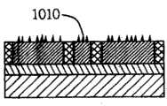
图10A描绘了根据本发明一实施例应用之在活性区表面粗糙化后之剖面图。FIG. 10A depicts a cross-sectional view after surface roughening of the active area applied according to one embodiment of the present invention.
图10B描绘了根据本发明一实施例应用之在活性区表面形成2维光子晶体后之剖面图。FIG. 10B depicts a cross-sectional view of a 2D photonic crystal formed on the surface of the active region according to an embodiment of the present invention.
图11A描绘了根据本发明一实施例应用之在图10A中形成第二电极之剖面图。FIG. 11A depicts a cross-sectional view of the second electrode formed in FIG. 10A applied in accordance with an embodiment of the present invention.
图11B描绘了根据本发明一实施例应用之在图10B中形成第二电极之剖面图。FIG. 11B depicts a cross-sectional view of the second electrode formed in FIG. 10B applied in accordance with an embodiment of the present invention.
图12A描绘了根据本发明一实施例应用之切割图11A之发光装置之剖面图。FIG. 12A depicts a cross-sectional view of the light emitting device of FIG. 11A applied according to an embodiment of the present invention.
图12B描绘了根据本发明一实施例应用之切割图11B之发光装置之剖面图。FIG. 12B depicts a cross-sectional view of cutting the light emitting device of FIG. 11B applied according to an embodiment of the present invention.
具体实施方式Detailed ways
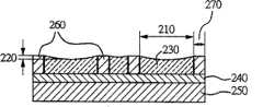
图1显示了一种传统半导体架构,其包含活性区130、电极层140以及载体150。当实施传统之化学机械抛光技术时,若欲抛光之平面两侧距离L110过大,将造成平面两侧与中心位置之变异值V120过大,所以平面两侧距离L与变异值V成正比。FIG. 1 shows a conventional semiconductor structure, which includes an
图2显示了一种具有停止点260之半导体架构,其包含欲抛光之平面两侧距离L210、变异值V220、活性区230、电极层240载体250以及停止点宽度a270。也是本发明在实施超平坦化学机械抛光技术后的一个实施例,若在植入复数个抛光停止点260后,则整个平面之变异值V将可以控制在半导体制程所要求的标准中。该方法包含以下步骤:(a)提供一第一物质,用于形成一第一层;(b)提供一第二物质,用于在该第一层之一面上形成一第二层;(c)蚀刻该第二层,用于产生复数个露出该第一层的表面之沟槽;(d)填充一硬度大于该第一物质及该第二物质之第三物质于该等沟槽中形成复数个抛光停止点;以及(e)移除该等沟槽外之该第三物质,而暴露出该第二层之表面。进一步而言,本实施例仍可以类似步骤移除该第一物质且可以控制变异值V在半导体制程所要求的标准中。2 shows a semiconductor structure with a
图3显示了根据本发明一实施例应用之停止点分布图之剖面图。由于如上所述之遇抛光平面的两侧之距离与变异值成正比。于是在控制了停止点之大小以及停止点与停止点间之距离后,可以获得在标准范围内之变异值。当然,本实施例中之停止点之图形可以是圆形、三角形、矩形或其它几何图形。Figure 3 shows a cross-sectional view of a stop point profile applied in accordance with an embodiment of the present invention. As mentioned above, the distance between the two sides of the polishing plane is directly proportional to the variation value. Therefore, after controlling the size of the stop point and the distance between the stop point and the stop point, the variation value within the standard range can be obtained. Certainly, the figure of the stopping point in this embodiment may be a circle, a triangle, a rectangle or other geometric figures.
根据本发明的一种应用,图4-图12揭示了另一实施例中,其是一种制造薄膜半导体发光装置之方法,该方法包含以下步骤:(a)提供一第一物质,用于形成一第一层410;(b)提供一半导体材料之第二物质,用于在该第一层之一面上形成一做为活性区(active region)之第二层230;(如图4中所示)(c)蚀刻该第二层,用于产生复数个露出该第一层的表面之沟槽510;(如图5中所示)(d)覆盖一层介质620;(e)填充一硬度大于该第一物质及该第二物质之第三物质610于该等沟槽中形成复数个抛光停止点;(如图6中所示)(f)提供一第四物质,用于在该第二层之表面上形成一第一电极层710;(如图7中所示)(g)黏接该第一电极层至一电导式载体810上;(如图8中所示)(h)移除该第一层露出复数个抛光停止点910;(如图9中所示)以及(i)在移除该第一层后之该第二物质之表面上形成复数个第二电极1110。(如图11中所示)。本实施例中进一步包含如图10A在活性区表面粗糙化1010或图10B在活性区表面形成2维光子晶体1020之步骤。最后如图12A或12B所示再对发光装置进行切割。上述之实施例中,该第一物质可以为蓝宝石、该第二物质可以为氮化镓或氮化铟镓、该第二物质可以为III-V族或II-VI之半导体材料、(c)步骤中之蚀刻可以是感应耦合电浆蚀刻、其中该第三物质可以是钻石薄膜或类金刚石薄膜、(h)步骤中之移除可以是使用机械研磨或化学机械抛光、该第一电极层可以是P型以及该第二电极层可以是N型。本发明之一实施例,钻石肩发光二极管如符号1210所示。According to an application of the present invention, FIG. 4-FIG. 12 discloses another embodiment, which is a method for manufacturing a thin-film semiconductor light-emitting device. The method includes the following steps: (a) providing a first substance for Form a
依本发明之一实施例所制作之半导体装置结构包含:一电导性载体;一半导体材料层;一超硬材料,其中该超硬材料至少有一表面相邻于该半导体材料层;一第一电极层,其位于该半导体材料层之一表面上;以及一第二电极层,其相对于该第一电极层位于该半导体材料层之另一表面上。其中该半导体材料层包含氮化铝镓铟(AlInGaN)、磷化铝镓铟(AlInGaP)、砷化铝镓(AlGaAs)、磷化砷镓(GaAsP)或磷化砷镓铟;该超硬材料包含钻石、类钻膜(DLC)、氮化钛类(TiNx)或钛钨合金类(TiWx)以及该电导性载体包含铜、硅、碳化硅或砷化镓。A semiconductor device structure manufactured according to an embodiment of the present invention includes: an electrically conductive carrier; a semiconductor material layer; a superhard material, wherein at least one surface of the superhard material is adjacent to the semiconductor material layer; a first electrode layer on one surface of the layer of semiconductor material; and a second electrode layer on the other surface of the layer of semiconductor material relative to the first electrode layer. Wherein the semiconductor material layer includes aluminum gallium indium nitride (AlInGaN), aluminum gallium indium phosphide (AlInGaP), aluminum gallium arsenide (AlGaAs), gallium arsenide phosphide (GaAsP) or gallium indium gallium arsenide phosphide; the superhard material It includes diamond, diamond-like film (DLC), titanium nitride (TiNx) or titanium-tungsten alloy (TiWx) and the conductive carrier includes copper, silicon, silicon carbide or gallium arsenide.
Claims (15)
Priority Applications (4)
| Application Number | Priority Date | Filing Date | Title |
|---|---|---|---|
| CN2007100802816ACN101244533B (en) | 2007-02-16 | 2007-02-16 | Method of ultra-flat chemical mechanical polishing technique and semiconductor device manufactured using the same |
| TW096123544ATWI365492B (en) | 2007-02-16 | 2007-06-28 | Super flat chemical mechanical polishing (sf-cmp) technology for thin film gan devices |
| US11/891,466US8415186B2 (en) | 2007-02-16 | 2007-08-10 | Method of super flat chemical mechanical polishing technology and semiconductor elements produced thereof |
| US12/415,467US7985971B2 (en) | 2007-02-16 | 2009-03-31 | Method of producing thin semiconductor structures |
Applications Claiming Priority (1)
| Application Number | Priority Date | Filing Date | Title |
|---|---|---|---|
| CN2007100802816ACN101244533B (en) | 2007-02-16 | 2007-02-16 | Method of ultra-flat chemical mechanical polishing technique and semiconductor device manufactured using the same |
Related Child Applications (1)
| Application Number | Title | Priority Date | Filing Date |
|---|---|---|---|
| CN2010102430453ADivisionCN102054682B (en) | 2007-02-16 | 2007-02-16 | Semiconductor light emitting device and manufacturing method thereof |
Publications (2)
| Publication Number | Publication Date |
|---|---|
| CN101244533A CN101244533A (en) | 2008-08-20 |
| CN101244533Btrue CN101244533B (en) | 2010-09-15 |
Family
ID=39705873
Family Applications (1)
| Application Number | Title | Priority Date | Filing Date |
|---|---|---|---|
| CN2007100802816AActiveCN101244533B (en) | 2007-02-16 | 2007-02-16 | Method of ultra-flat chemical mechanical polishing technique and semiconductor device manufactured using the same |
Country Status (3)
| Country | Link |
|---|---|
| US (1) | US8415186B2 (en) |
| CN (1) | CN101244533B (en) |
| TW (1) | TWI365492B (en) |
Families Citing this family (11)
| Publication number | Priority date | Publication date | Assignee | Title |
|---|---|---|---|---|
| US7985971B2 (en)* | 2007-02-16 | 2011-07-26 | Hong Kong Applied Science And Technology Research Institute Co. Ltd. | Method of producing thin semiconductor structures |
| US8222064B2 (en) | 2007-08-10 | 2012-07-17 | Hong Kong Applied Science and Technology Research Institute Company Limited | Vertical light emitting diode device structure and method of fabricating the same |
| US8187900B2 (en)* | 2007-08-10 | 2012-05-29 | Hong Kong Applied Science and Technology Research Institute Company Limited | Optimization of polishing stop design |
| CN102637788B (en)* | 2008-06-02 | 2014-06-25 | 香港应用科技研究院有限公司 | Semiconductor wafer and semiconductor device |
| DE102009035429A1 (en)* | 2009-07-31 | 2011-02-03 | Osram Opto Semiconductors Gmbh | LED chip |
| CN102117866B (en)* | 2009-12-31 | 2013-01-09 | 香港应用科技研究院有限公司 | Semiconductor wafer and semiconductor device, and method for manufacturing semiconductor wafer and device |
| CN102339911B (en)* | 2010-07-23 | 2015-03-18 | 赛恩倍吉科技顾问(深圳)有限公司 | Manufacturing method for light emitting diode |
| US9054063B2 (en)* | 2013-04-05 | 2015-06-09 | Infineon Technologies Ag | High power single-die semiconductor package |
| KR102235612B1 (en) | 2015-01-29 | 2021-04-02 | 삼성전자주식회사 | Semiconductor device having work-function metal and method of forming the same |
| CN115548864A (en)* | 2022-09-15 | 2022-12-30 | 深圳斯玛特传感技术有限公司 | Laser and preparation method thereof |
| TW202437367A (en)* | 2022-11-22 | 2024-09-16 | 美商應用材料股份有限公司 | Method for collective dishing of singulated dies |
Citations (3)
| Publication number | Priority date | Publication date | Assignee | Title |
|---|---|---|---|---|
| US5332467A (en)* | 1993-09-20 | 1994-07-26 | Industrial Technology Research Institute | Chemical/mechanical polishing for ULSI planarization |
| US6348395B1 (en)* | 2000-06-07 | 2002-02-19 | International Business Machines Corporation | Diamond as a polish-stop layer for chemical-mechanical planarization in a damascene process flow |
| CN1383201A (en)* | 2001-04-24 | 2002-12-04 | 华邦电子股份有限公司 | Method for manufacturing shallow groove isolation structure |
Family Cites Families (10)
| Publication number | Priority date | Publication date | Assignee | Title |
|---|---|---|---|---|
| US5246884A (en)* | 1991-10-30 | 1993-09-21 | International Business Machines Corporation | Cvd diamond or diamond-like carbon for chemical-mechanical polish etch stop |
| US6776917B2 (en)* | 2001-01-03 | 2004-08-17 | International Business Machines Corporation | Chemical mechanical polishing thickness control in magnetic head fabrication |
| US6611002B2 (en)* | 2001-02-23 | 2003-08-26 | Nitronex Corporation | Gallium nitride material devices and methods including backside vias |
| US6828584B2 (en)* | 2001-05-18 | 2004-12-07 | Semiconductor Energy Laboratory Co., Ltd. | Semiconductor device and method for manufacturing the same |
| US6455340B1 (en) | 2001-12-21 | 2002-09-24 | Xerox Corporation | Method of fabricating GaN semiconductor structures using laser-assisted epitaxial liftoff |
| JP3962282B2 (en)* | 2002-05-23 | 2007-08-22 | 松下電器産業株式会社 | Manufacturing method of semiconductor device |
| JP2007525016A (en) | 2003-07-14 | 2007-08-30 | アリージス・テクノロジーズ・インコーポレーテッド | Method for treating gallium nitride |
| US7001824B2 (en) | 2004-02-20 | 2006-02-21 | Supernova Optoelectronics Corporation | Gallium nitride vertical light emitting diode structure and method of separating a substrate and a thin film in the structure |
| JP4368225B2 (en)* | 2004-03-10 | 2009-11-18 | 三洋電機株式会社 | Method for manufacturing nitride-based semiconductor light-emitting device |
| TWI308396B (en)* | 2005-01-21 | 2009-04-01 | Epistar Corp | Light emitting diode and fabricating method thereof |
- 2007
- 2007-02-16CNCN2007100802816Apatent/CN101244533B/enactiveActive
- 2007-06-28TWTW096123544Apatent/TWI365492B/enactive
- 2007-08-10USUS11/891,466patent/US8415186B2/enactiveActive
Patent Citations (3)
| Publication number | Priority date | Publication date | Assignee | Title |
|---|---|---|---|---|
| US5332467A (en)* | 1993-09-20 | 1994-07-26 | Industrial Technology Research Institute | Chemical/mechanical polishing for ULSI planarization |
| US6348395B1 (en)* | 2000-06-07 | 2002-02-19 | International Business Machines Corporation | Diamond as a polish-stop layer for chemical-mechanical planarization in a damascene process flow |
| CN1383201A (en)* | 2001-04-24 | 2002-12-04 | 华邦电子股份有限公司 | Method for manufacturing shallow groove isolation structure |
Non-Patent Citations (1)
| Title |
|---|
| US 2002/0001958 A1,全文. |
Also Published As
| Publication number | Publication date |
|---|---|
| CN101244533A (en) | 2008-08-20 |
| US20080197367A1 (en) | 2008-08-21 |
| US8415186B2 (en) | 2013-04-09 |
| TW200822197A (en) | 2008-05-16 |
| TWI365492B (en) | 2012-06-01 |
Similar Documents
| Publication | Publication Date | Title |
|---|---|---|
| CN101244533B (en) | Method of ultra-flat chemical mechanical polishing technique and semiconductor device manufactured using the same | |
| US10510577B2 (en) | Lift off process for chip scale package solid state devices on engineered substrate | |
| TWI429104B (en) | Method for fabricating a vertical light emitting diode structure | |
| US7985971B2 (en) | Method of producing thin semiconductor structures | |
| US7776637B2 (en) | Method of manufacturing light emitting diodes | |
| US8236584B1 (en) | Method of forming a light emitting diode emitter substrate with highly reflective metal bonding | |
| US9899578B2 (en) | Process for preparing a semiconductor structure for mounting | |
| JP2007517404A (en) | Sapphire laser lift-off from nitride flip chip | |
| KR101811673B1 (en) | Method of forming a dielectric layer on a semiconductor light emitting device | |
| CN101681975B (en) | Main substrate of nitride-based light emitting device | |
| CN101617415B (en) | Method for manufacturing thin film semiconductor structure | |
| US8222064B2 (en) | Vertical light emitting diode device structure and method of fabricating the same | |
| JP5817503B2 (en) | Nitride semiconductor light emitting device and manufacturing method thereof | |
| CN102054682B (en) | Semiconductor light emitting device and manufacturing method thereof | |
| WO2012113205A1 (en) | Vertical light emitting diode device structure and method of fabricating the same | |
| US20100244195A1 (en) | Host substrate for nitride based light emitting devices | |
| CN102369604B (en) | Vertical structure light emitting diode structure and manufacturing method thereof | |
| TWI433349B (en) | Vertical light emitting diode device structure and method of fabricating the same | |
| HK1166551A (en) | Vertical light emitting diode device structure and method of fabricating the same | |
| CN104704642A (en) | Method for producing an optoelectronic component |
Legal Events
| Date | Code | Title | Description |
|---|---|---|---|
| C06 | Publication | ||
| PB01 | Publication | ||
| C10 | Entry into substantive examination | ||
| SE01 | Entry into force of request for substantive examination | ||
| C14 | Grant of patent or utility model | ||
| GR01 | Patent grant |