CN101243421A - System and method for transferring instructions and data between a processor and an external device - Google Patents
System and method for transferring instructions and data between a processor and an external deviceDownload PDFInfo
- Publication number
- CN101243421A CN101243421ACNA200680030145XACN200680030145ACN101243421ACN 101243421 ACN101243421 ACN 101243421ACN A200680030145X ACNA200680030145X ACN A200680030145XACN 200680030145 ACN200680030145 ACN 200680030145ACN 101243421 ACN101243421 ACN 101243421A
- Authority
- CN
- China
- Prior art keywords
- channel
- processor
- event
- read
- write
- Prior art date
- Legal status (The legal status is an assumption and is not a legal conclusion. Google has not performed a legal analysis and makes no representation as to the accuracy of the status listed.)
- Granted
Links
Images


Classifications
- G—PHYSICS
- G06—COMPUTING OR CALCULATING; COUNTING
- G06F—ELECTRIC DIGITAL DATA PROCESSING
- G06F13/00—Interconnection of, or transfer of information or other signals between, memories, input/output devices or central processing units
- G06F13/14—Handling requests for interconnection or transfer
- G06F13/20—Handling requests for interconnection or transfer for access to input/output bus
- G06F13/24—Handling requests for interconnection or transfer for access to input/output bus using interrupt
Landscapes
- Engineering & Computer Science (AREA)
- Theoretical Computer Science (AREA)
- Physics & Mathematics (AREA)
- General Engineering & Computer Science (AREA)
- General Physics & Mathematics (AREA)
- Memory System Of A Hierarchy Structure (AREA)
- Bus Control (AREA)
- Mobile Radio Communication Systems (AREA)
Abstract
Translated fromChinese
Description
Translated fromChinese技术领域technical field
本发明一般地涉及改进的数据处理系统和方法。更具体地说,本发明涉及用于在处理器与外部设备之间传送指令和数据的系统和方法。The present invention generally relates to improved data processing systems and methods. More specifically, the present invention relates to systems and methods for transferring instructions and data between a processor and external devices.
背景技术Background technique
通常,在现有技术中,当CPU或其他处理单元(PU)在等待程序外部的某一事件时,操作系统或活动程序将运行轮询循环,它在此循环中将保持读取PU以及程序使用的事件寄存器,直到它所等待的事件发生。当程序运行时,PU在轮询事件寄存器并且未执行有用的工作。Typically, in prior art, when a CPU or other processing unit (PU) is waiting for some event outside the program, the operating system or active program will run a polling loop where it will keep reading from the PU and the program Use the event register until the event it is waiting for occurs. While the program is running, the PU is polling the event register and not performing useful work.
典型的现代处理器通常使用虚拟存储器以及外部设备的存储器映射来进行此通信。另一方面,一些处理器(尤其是在多处理器环境中)仅具有访问本地存储器的权限,而没有访问虚拟存储器的权限。本地存储器是有限的,并且在典型的多处理器配置中,加载和存储操作无法访问此本地存储器外部的存储器。因此,当等待来自外部设备的响应时,限制了针对其他PU功能使用本地存储器。如果一个PU同时等待来自若干设备的通信响应,甚至会进一步限制用于其他功能的可用存储器。A typical modern processor usually uses virtual memory and a memory map of the external device for this communication. On the other hand, some processors (especially in multiprocessor environments) only have access to local memory, not virtual memory. Local memory is limited, and in typical multiprocessor configurations, load and store operations cannot access memory outside of this local memory. Therefore, the use of local memory for other PU functions is limited when waiting for a response from an external device. If a PU waits for communication responses from several devices at the same time, it can even further limit the available memory for other functions.
存储器还可以用于跟踪入站或出站寄存器中是否存在有效数据。有效数据是已放置在寄存器中以供接收设备使用但接收设备尚未访问的数据。因此,从以上可知,在多数现代计算设备中,存储器资源存在许多损耗。The memory can also be used to track the presence of valid data in the inbound or outbound registers. Valid data is data that has been placed in a register for use by the receiving device but has not yet been accessed by the receiving device. Thus, from the above it can be seen that in most modern computing devices there is a lot of wear and tear on memory resources.
发明内容Contents of the invention
鉴于以上所述,具有一种用于在处理器与处理器外部的其他设备(例如,其他处理器、输入/输出(I/O)设备等)之间通信的系统和方法是有利的,其中此类通信不会加重处理器的本地或虚拟存储器的负担。此外,具有一种允许在等待数据或事件时将处理器置于低功率状态的系统和方法是有利的。In view of the foregoing, it would be advantageous to have a system and method for communicating between a processor and other devices external to the processor (e.g., other processors, input/output (I/O) devices, etc.), wherein Such communications do not tax the processor's local or virtual memory. Furthermore, it would be advantageous to have a system and method that allows a processor to be placed in a low power state while waiting for data or an event.
本发明提供了一种用于在处理器和外部设备之间传送指令和数据的系统和方法和/或一种用于与处理器事件设备通信的系统和方法。本发明的系统和方法使用通道接口作为在处理器和存储器流控制器之间通信的主要机制。所述通道接口提供用于例如与处理器设备、存储器流控制设备、机器状态寄存器以及外部处理器中断设备进行通信的通道。这些通道用于降低处理器的本地存储的负担以及使总线通信量最小化。The present invention provides a system and method for transferring instructions and data between a processor and an external device and/or a system and method for communicating with a processor event device. The systems and methods of the present invention use a channel interface as the primary mechanism for communication between the processor and the memory flow controller. The channel interface provides channels for communicating with, for example, processor devices, memory flow control devices, machine status registers, and external processor interrupt devices. These channels are used to offload the processor's local storage and to minimize bus traffic.
可以将这些通道指定为阻塞或非阻塞。对于阻塞通道,当没有可从相应寄存器读取的数据时,或没有可供写入相应寄存器的空间时,将处理器置于低功率“停止”状态。当数据变得可用或空间被释放时,通过跨阻塞通道的通信自动唤醒处理器。因此,本发明的通道允许将处理器保持在低功率状态,而不是如现有技术系统那样不断轮询或遍历事件寄存器。These channels can be specified as blocking or non-blocking. For blocking channels, the processor is placed in a low-power "halt" state when there is no data to read from, or space to write to, the corresponding register. Processors are automatically woken up by communicating across blocked channels when data becomes available or space is freed. Thus, the channel of the present invention allows the processor to be kept in a low power state, rather than constantly polling or walking event registers as in prior art systems.
本发明的这些和其他特征和优点将在以下对本发明的示意性实施例的详细说明中进行描述,或者鉴于以下详细说明,本发明的这些和其他特征和优点将对本领域的技术人员变得显而易见。These and other features and advantages of the invention will be described in, or will become apparent to those skilled in the art in view of, the following detailed description of the illustrative embodiments of the invention .
附图说明Description of drawings
在所附权利要求中说明了被认为是本发明特性的新颖特征。但是,当结合附图阅读时,通过参考以下对示例性实施例的详细说明,可以最佳地理解发明本身及其优选使用方式、进一步的目的和优点,这些附图是:The novel features believed characteristic of the invention are set forth in the appended claims. However, the invention itself, its preferred modes of use, further objects and advantages, are best understood by reference to the following detailed description of exemplary embodiments when read in conjunction with the accompanying drawings:
图1是根据本发明的示意性实施例的宽带处理器体系结构(BPA)的示意性方块图;1 is a schematic block diagram of a Broadband Processor Architecture (BPA) according to an exemplary embodiment of the present invention;
图2是根据本发明的示意性实施例的典型MFC 200的示意性方块图;Figure 2 is a schematic block diagram of a typical MFC 200 according to an exemplary embodiment of the present invention;
图3A是示出了根据本发明的示意性实施例的MFC命令的参数助记符的示意图;3A is a schematic diagram showing parameter mnemonics of MFC commands according to an exemplary embodiment of the present invention;
图3B是示出了根据本发明的示意性实施例的DMA列表命令的详细信息的示意图;3B is a schematic diagram showing detailed information of a DMA list command according to an exemplary embodiment of the present invention;
图4是示出了根据美国专利申请公开No.2004/0264445中所述机制的关于单对通道的通道电路的SPU发出和控制逻辑以及数据流的布置的示意图;FIG. 4 is a schematic diagram illustrating the arrangement of SPU issue and control logic and data flow for channel circuits of a single pair of channels according to the mechanism described in U.S. Patent Application Publication No. 2004/0264445;
图5提供了示出根据本发明的示意性实施例的通道接口的示意性操作的流程图;FIG. 5 provides a flow diagram illustrating the exemplary operation of a channel interface according to an exemplary embodiment of the present invention;
图6A是示出了本发明的一个实施例使用通道的方式的示意图;Figure 6A is a schematic diagram illustrating the manner in which channels are used by one embodiment of the present invention;
图6B和6C示出了根据本发明的一个示意性实施例的列出SPU通道图的示意图;6B and 6C show schematic diagrams listing SPU channel maps according to an exemplary embodiment of the present invention;
图7A是示出了根据本发明的一个示意性实施例的MFC命令操作码通道的详细信息的示意图;FIG. 7A is a schematic diagram showing detailed information of an MFC command opcode channel according to an exemplary embodiment of the present invention;
图7B是示出了根据本发明的一个示意性实施例的MFC类ID通道的详细信息的示意图;7B is a schematic diagram showing detailed information of an MFC class ID channel according to an exemplary embodiment of the present invention;
图7C示出了根据本发明的一个示意性实施例的用于8路、成组相联(set associative)高速缓存的典型RMT表项;FIG. 7C shows a typical RMT entry for 8-way, set associative (set associative) cache according to an exemplary embodiment of the present invention;
图7D是示出了根据本发明的一个示意性实施例的MFC命令标记标识通道的详细信息的示意图;FIG. 7D is a schematic diagram showing detailed information of an MFC command tag identification channel according to an exemplary embodiment of the present invention;
图7E是示出了根据本发明的一个示意性实施例的MFC传输大小或列表大小通道的详细信息的示意图;FIG. 7E is a schematic diagram showing detailed information of an MFC transfer size or list size channel according to an exemplary embodiment of the present invention;
图7F是示出了根据本发明的一个示意性实施例的MFC本地存储地址通道的详细信息的示意图;FIG. 7F is a schematic diagram showing detailed information of an MFC local storage address channel according to an exemplary embodiment of the present invention;
图7G是示出了根据本发明的一个示意性实施例的MFC有效低地址或列表地址通道的详细信息的示意图;FIG. 7G is a schematic diagram showing detailed information of an MFC effective low address or list address channel according to an exemplary embodiment of the present invention;
图7H是示出了根据本发明的一个示意性实施例的MFC有效高地址通道的详细信息的示意图;FIG. 7H is a schematic diagram showing detailed information of an MFC effective high address channel according to an exemplary embodiment of the present invention;
图8是示出了根据本发明的一个示意性实施例的用于写入MFC命令参数的示意性操作的流程图;FIG. 8 is a flowchart illustrating an exemplary operation for writing MFC command parameters according to an exemplary embodiment of the present invention;
图9A是示出了根据本发明的一个示意性实施例的MFC写入标记组查询掩码通道的详细信息的示意图;FIG. 9A is a schematic diagram showing detailed information of an MFC write tag group query mask channel according to an exemplary embodiment of the present invention;
图9B是示出了根据本发明的一个示意性实施例的MFC读取标记组查询掩码通道的详细信息的示意图;FIG. 9B is a schematic diagram showing detailed information of an MFC read tag group query mask channel according to an exemplary embodiment of the present invention;
图9C是示出了根据本发明的一个示意性实施例的MFC写入标记状态更新请求通道的详细信息的示意图;FIG. 9C is a schematic diagram showing detailed information of an MFC write flag status update request channel according to an exemplary embodiment of the present invention;
图9D是示出了根据本发明的一个示意性实施例的MFC读取标记组状态通道的详细信息的示意图;FIG. 9D is a schematic diagram showing the detailed information of the MFC read tag group status channel according to an exemplary embodiment of the present invention;
图9E是示出了根据本发明的一个示意性实施例的MFC读取列表停止和通知标记状态通道的详细信息的示意图;FIG. 9E is a schematic diagram showing detailed information of the MFC read list stop and notification mark status channel according to an exemplary embodiment of the present invention;
图9F是示出了根据本发明的一个示意性实施例的MFC写入列表停止和通知标记确认通道的详细信息的示意图;FIG. 9F is a schematic diagram showing the detailed information of the MFC write list stop and notification mark confirmation channel according to an exemplary embodiment of the present invention;
图9G是示出了根据本发明的一个示意性实施例的MFC读取原子命令状态通道的详细信息的示意图;FIG. 9G is a schematic diagram showing the detailed information of the MFC reading the atomic command status channel according to an exemplary embodiment of the present invention;
图10是示出了根据本发明的示意性实施例的用于轮询一个MFC命令的完成或一组MFC命令的完成的示意性操作的流程图;FIG. 10 is a flowchart illustrating exemplary operations for polling for completion of an MFC command or a group of MFC commands, according to an exemplary embodiment of the present invention;
图11是示出了根据本发明的示意性实施例的用于等待标记组更新或等待事件(一个或多个标记组完成)的示意性操作的流程图;11 is a flowchart illustrating exemplary operations for waiting for a tag set update or waiting for an event (one or more tag sets complete) in accordance with an exemplary embodiment of the present invention;
图12是示出了根据本发明的示意性实施例的用于使用SPU事件设备作为备选方案以等待或轮询条件标记事件的示意性操作的流程图;FIG. 12 is a flowchart illustrating exemplary operations for using the SPU event device as an alternative to wait or poll for conditional flag events, according to an exemplary embodiment of the present invention;
图13是示出了根据本发明的示意性实施例的用于轮询以判定MFC DMA列表命令是否已到达设置了停止和通知标志的列表元素的示意性操作的流程图;Fig. 13 is a flow chart showing an exemplary operation for polling to determine whether an MFC DMA list command has arrived at a list element that has set a stop and a notification flag according to an exemplary embodiment of the present invention;
图14是示出了根据本发明的一个示意性实施例的用于等待MFC DMA列表命令到达设置了停止和通知标志的列表元素的示意性操作的流程图;FIG. 14 is a flow chart showing an exemplary operation for waiting for an MFC DMA list command to arrive at a list element with a stop and a notification flag according to an exemplary embodiment of the present invention;
图15是示出了根据本发明的示意性实施例的用于使用SPU事件设备作为备选方案以等待或轮询列表停止和通知标记组状态的示意性操作的流程图;FIG. 15 is a flowchart illustrating exemplary operations for using the SPU event device as an alternative to wait or poll for list stop and notify flag group status, according to an exemplary embodiment of the present invention;
图16是示出了根据本发明的一个示意性实施例的MFC写入多源同步请求通道的详细信息的示意图;FIG. 16 is a schematic diagram showing detailed information written by MFC to a multi-source synchronization request channel according to an exemplary embodiment of the present invention;
图17A是示出了根据本发明的一个示意性实施例的SPU写入出站邮箱通道的详细信息的示意图;FIG. 17A is a schematic diagram showing detailed information written by an SPU to an outbound mailbox channel according to an exemplary embodiment of the present invention;
图17B是示出了根据本发明的一个示意性实施例的SPU写入出站中断邮箱通道的详细信息的示意图;Fig. 17B is a schematic diagram showing detailed information written by an SPU to an outbound interrupt mailbox channel according to an exemplary embodiment of the present invention;
图17C是示出了根据本发明的一个示意性实施例的SPU读取入站邮箱通道的详细信息的示意图;FIG. 17C is a schematic diagram illustrating an SPU reading detailed information of an inbound mailbox channel according to an exemplary embodiment of the present invention;
图18是示出了根据本发明的一个示意性实施例的SPU信号通知通道的详细信息的示意图;FIG. 18 is a schematic diagram showing detailed information of an SPU signaling channel according to an exemplary embodiment of the present invention;
图19A是示出了根据本发明的一个示意性实施例的SPU写入递减器通道的详细信息的示意图;FIG. 19A is a schematic diagram showing detailed information written by an SPU to a decrementer channel according to an exemplary embodiment of the present invention;
图19B是示出了根据本发明的一个示意性实施例的SPU读取递减器通道的详细信息的示意图;FIG. 19B is a schematic diagram illustrating an SPU reading detailed information of decrementer channels according to an exemplary embodiment of the present invention;
图20A是示出了根据本发明的一个示意性实施例的SPU读取机器状态通道的详细信息的示意图;FIG. 20A is a schematic diagram illustrating an SPU reading detailed information of a machine state channel according to an exemplary embodiment of the present invention;
图20B是示出了根据本发明的一个示意性实施例的SPU写入状态保存和恢复通道的详细信息的示意图;FIG. 20B is a schematic diagram showing detailed information of an SPU write state preservation and restoration channel according to an exemplary embodiment of the present invention;
图20C是示出了根据本发明的一个示意性实施例的SPU读取状态保存和恢复通道的详细信息的示意图;FIG. 20C is a schematic diagram showing detailed information of an SPU read state preservation and recovery channel according to an exemplary embodiment of the present invention;
图21是示出了根据本发明的一个示意性实施例的SPU事件设备的逻辑表示的示意性方块图;Figure 21 is a schematic block diagram showing a logical representation of an SPU event device according to an exemplary embodiment of the present invention;
图22A是示出了根据本发明的一个示意性实施例的SPU读取事件状态通道的详细信息的示意图;22A is a schematic diagram showing detailed information of an SPU read event status channel according to an exemplary embodiment of the present invention;
图22B是示出了根据本发明的一个示意性实施例的SPU写入事件掩码通道的详细信息的示意图;22B is a schematic diagram showing detailed information of an SPU write event mask channel according to an exemplary embodiment of the present invention;
图22C是示出了根据本发明的一个示意性实施例的SPU读取事件掩码通道的详细信息的示意图;FIG. 22C is a schematic diagram showing detailed information of an SPU read event mask channel according to an exemplary embodiment of the present invention;
图22D是示出了根据本发明的一个示意性实施例的SPU写入事件确认通道的详细信息的示意图;22D is a schematic diagram showing detailed information of an SPU write event confirmation channel according to an exemplary embodiment of the present invention;
图23是示出了根据本发明的一个实施例的用于处理MFC DMA列表命令停止和通知事件的示意性操作的流程图;Fig. 23 is a flow chart showing the schematic operation for processing MFC DMA list command stop and notification event according to one embodiment of the present invention;
图24是示出了根据本发明的一个实施例的用于处理MFC SPU命令队列可用事件的示意性操作的流程图;FIG. 24 is a flow chart showing a schematic operation for processing an MFC SPU command queue available event according to one embodiment of the present invention;
图25是示出了根据本发明的一个实施例的用于处理SPU入站邮箱可用事件的示意性操作的流程图;FIG. 25 is a flow diagram illustrating exemplary operations for processing an SPU inbound mailbox availability event according to one embodiment of the invention;
图26是示出了根据本发明的一个实施例的用于处理SPU递减器事件的示意性操作的流程图;FIG. 26 is a flowchart illustrating exemplary operations for handling SPU decrementer events according to one embodiment of the present invention;
图27是示出了根据本发明的一个实施例的用于处理SPU出站中断邮箱可用事件的示意性操作的流程图;FIG. 27 is a flowchart illustrating exemplary operations for handling an SPU outbound interrupt mailbox availability event according to one embodiment of the present invention;
图28是示出了根据本发明的一个实施例的用于处理SPU出站邮箱可用事件的示意性操作的流程图;FIG. 28 is a flowchart illustrating exemplary operations for handling an SPU outbound mailbox availability event according to one embodiment of the present invention;
图29是示出了根据本发明的一个实施例的用于处理SPU信号通知2可用事件的示意性操作的流程图;FIG. 29 is a flow diagram illustrating exemplary operations for processing an
图30是示出了根据本发明的一个实施例的用于处理SPU信号通知1可用事件的示意性操作的流程图;FIG. 30 is a flow chart illustrating exemplary operations for processing an
图31是示出了根据本发明的一个示意性实施例的用于处理锁定线保留丢失事件的示意性操作的流程图;FIG. 31 is a flowchart illustrating exemplary operations for handling a lock line reservation loss event according to an exemplary embodiment of the present invention;
图32是示出了根据本发明的一个示意性实施例的用于处理特权关注事件的示意性操作的流程图;FIG. 32 is a flowchart illustrating an exemplary operation for handling a privileged concern event according to an exemplary embodiment of the present invention;
图33是示出了根据本发明的一个实施例的用于处理多源同步事件的示意性操作的流程图。FIG. 33 is a flowchart illustrating exemplary operations for handling a multi-source synchronization event according to one embodiment of the present invention.
具体实施方式Detailed ways
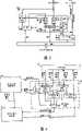
图1是其中可以实现本发明的各方面的数据处理系统的示意性方块图。图1所示的示意性数据处理系统是异构宽带处理器体系结构(例如,可从国际商业机器公司获得的CELL宽带引擎处理器)的实施方式的实例。虽然宽带处理器体系结构(BPA)将用于本发明的优选实施例的描述,但是如本领域的技术人员在阅读以下说明时将容易地理解的,本发明并不限于此。Figure 1 is a schematic block diagram of a data processing system in which aspects of the present invention may be implemented. The illustrative data processing system shown in FIG. 1 is an example of an implementation of a heterogeneous broadband processor architecture, such as the CELL Broadband Engine processor available from International Business Machines Corporation. While the Broadband Processor Architecture (BPA) will be used in the description of the preferred embodiment of the present invention, as those skilled in the art will readily understand upon reading the following description, the present invention is not limited thereto.
如图1所示,BPA 100包括power处理器元件(PPE)110的异构布置,所述power处理器元件具有处理器(PPU)116及其L1和L2高速缓存112和114,以及多个协处理器元件(SPE)120-134,每个协处理器元件都具有其自己的处理器单元(SPU)140-154、存储器流控制(MFC)155-162、本地存储器或存储(LS)163-170,以及总线接口单元(BIU单元)180-194(其可以例如是组合直接存储器访问(DMA)、存储器管理单元(MMU)和总线接口单元)。还提供了高宽带内部元件互连总线(EIB)196、总线接口控制器(BIC)197和存储器接口控制器(MIC)198。宽带引擎100可以是片上系统,以便可以在单个微处理器芯片上提供图1中示出的每个元件。As shown in FIG. 1, the
BPA 100可以是片上系统,以便可以在单个微处理器芯片上提供图1中示出的每个元件。此外,BPA 100是每个SPU可在其中接收来自系统中的每个其他SPU的不同指令的异构处理环境。此外,用于SPU的指令集不同于PPU的指令集,例如,PPU可以执行基于精简指令集计算机(RISC)的指令,而SPU执行矢量化指令。
SPE 120-134通过EIB 196相互连接并连接到L2高速缓存114。此外,SPE 120-134通过EIB 196连接到MIC 198和BIC 197。MIC 198提供到共享存储器199的通信接口。BIC 197在BPA 100与其他外部总线和设备之间提供通信接口。SPEs 120-134 are interconnected to each other and to
PPE 110是双线程PPE 110。此双线程PPE 110和八个SPE 120-134的组合使得BPA 100能够处理10个同时发生的线程以及超过128个未完成的存储器请求。PPE 110用作其他八个处理大多数计算工作负荷的SPE120-134的控制器。例如,PPE 110可以用于运行常规的操作系统,而SPE120-134执行矢量化浮点代码执行。
SPE 120-134包括协处理单元(SPU)140-154、存储器流控制单元155-162、本地存储器或存储163-174以及接口单元180-194。在一个示意性实施例中,本地存储器或存储163-174包括一个对PPE 110可见并可由软件直接寻址的256KB指令和数据存储器。SPEs 120-134 include co-processing units (SPUs) 140-154, memory flow control units 155-162, local memory or storage 163-174, and interface units 180-194. In one exemplary embodiment, local memory or storage 163-174 includes a 256KB instruction and data memory visible to
PPE 110可以使用小程序或线程加载SPE 120-134,从而将SPE链接在一起以处理复杂操作中的每个步骤。例如,集成了BPA 100的机顶盒可以加载程序以便读取DVD、进行视频和音频解码以及显示,并且数据将从SPE传递到SPE,直到它最终在输出显示器上显示。
存储器流控制单元(MFC)155-162用作SPU到系统的其余部分以及其他元件的接口。MFC 155-162提供了主存储和本地存储163-174之间的数据传输、保护和同步的主要机制。对于处理器中的每个SPU,逻辑上都存在一个MFC。某些实施方式可以在多个SPU之间共享单个MFC的资源。在这种情况下,为此MFC定义的所有设备和命令都必须显示为与每个SPU的软件的无关。共享MFC的效果限于与实施方式相关的设备和命令。Memory flow control units (MFCs) 155-162 serve as the interface of the SPU to the rest of the system and other elements. The MFC 155-162 provides the main mechanism for data transfer, protection and synchronization between main storage and local storage 163-174. There is logically one MFC for each SPU in the processor. Some implementations may share the resources of a single MFC among multiple SPUs. In this case, all devices and commands defined for this MFC must appear as independent of each SPU's software. The effect of sharing MFC is limited to implementation-dependent devices and commands.
存储器流控制(MFC)单元Memory Flow Control (MFC) unit
图2是根据本发明的示意性实施例的典型存储器流控制(MFC)单元200的示意性方块图。在此示意性实施例中,MFC 200具有两个到SPU的接口210和212、两个到总线接口单元(BIU)220的接口214和216,以及两个到可选SL1高速缓存230的接口222和224。SPU接口210和212是SPU通道接口210和SPU本地存储接口212。SPU通道接口210允许SPU访问MFC设备以及发出MFC命令。SPU本地存储接口212由MFC 200使用以访问SPU中的本地存储。一个到BIU 220的接口214允许存储器映射的I/O(MMIO)访问MFC设备。此接口214还允许其他处理器发出MFC命令。使用MMIO发出的命令被称为MFC代理命令。FIG. 2 is a schematic block diagram of a typical memory flow control (MFC) unit 200 according to an exemplary embodiment of the present invention. In this illustrative embodiment, MFC 200 has two
到SL1高速缓存的接口222和224主要用于数据传输。一个接口222由MFC 200使用以访问主存储中的地址转换表,另一个接口224用于在主存储和本地存储之间传输数据。
如图2所示,典型MFC中的主单元包括存储器映射的输入/输出(MMIO)接口240、MFC寄存器250和DMA控制器260。MMIO接口240将SPU的MFC设备映射到系统的实地址空间。这允许从系统中的任何处理器或任何设备访问MFC设备。此外,MMIO接口240可以配置为将SPU的本地存储映射到实地址空间。这允许从系统中的任何处理器或任何设备直接访问本地存储,从而能够进行本地存储到本地存储传输,并使I/O设备能够直接访问SPU的本地存储域。As shown in FIG. 2 , the main unit in a typical MFC includes a memory-mapped input/output (MMIO)
MFC寄存器单元250包含多数MFC设备。某些设备包含在直接存储器访问控制器(DMAC)260中。以下是MFC 200内的设备的列表。用户模式环境设备(即,可从非特权应用访问的环境设备)包括:(1)邮箱设备、(2)SPU信号通知设备、(3)代理标记组完成设备、(4)MFC多源同步设备、(5)SPU控制和状态设备,以及(6)SPU隔离设备。特权模式环境设备,即仅可由特权软件(例如操作系统)访问的设备,包括:(1)MFC状态寄存器1、(2)MFC逻辑分区ID寄存器、(3)MFC存储描述寄存器、(4)MFC数据地址寄存器、(5)MFC数据存储中断状态寄存器、(6)MFC地址比较控制寄存器、(7)MFC本地存储地址比较设备、(8)MFC命令错误寄存器、(9)MFC数据存储中断指针寄存器、(10)MFC控制寄存器、(11)MFC原子刷新(flush)寄存器、(12)SPU出站中断邮箱寄存器、(13)SPU特权设备、(14)SPU特权控制寄存器、(15)SPU本地存储限制寄存器、(16)SPU配置寄存器,以及(17)SPE上下文保存和恢复。The
下面将更详细地描述对本发明的机制尤为重要的设备,即邮箱设备、SPU信号通知设备、代理标记组完成设备、MFC多源同步设备、SPU通道访问设备、SPU事件设备以及中断设备。The devices that are particularly important to the mechanism of the present invention will be described in more detail below, namely the mailbox device, the SPU signaling device, the agent tag group completion device, the MFC multi-source synchronization device, the SPU channel access device, the SPU event device, and the interrupt device.
通常,MFC 200内的DMAC 260负责数据的同步和传输。DMAC 260可以在SPU的本地存储和主存储区域之间移动数据。可选地,数据可以缓存在SL1高速缓存中。Typically, the
SPE和PPE通过借助命令队列270和280之一将DMA命令请求排队到MFC来指示MFC 200执行这些DMA操作。由SPE发出的命令被排队到MFC SPU命令队列280。由PPE发出的命令被排队到MFC代理命令队列270。MFC使用存储器映射单元(MMU)290执行DMA传输所需的所有MFC地址转换和MFC访问保护检查。The SPE and PPE instruct the MFC 200 to perform these DMA operations by queuing DMA command requests to the MFC via one of the
MFC命令提供了使得在SPU中执行的代码能够访问主存储以及维护与系统中的其他处理器和设备的同步的主要方法。还提供了命令以管理可选的高速缓存。MFC命令可以由在SPU上运行的代码发出,或者由在其他处理器或设备(例如PPE)上运行的代码发出。在关联的SPU上运行的代码执行一系列通道指令以发出MFC命令。在其他处理器或设备上运行的代码执行一系列存储器映射的I/O(MMIO)传输以向SPE发出MFC命令。所发出的命令被排队到命令队列270和280之一。MFC commands provide the primary means by which code executing in the SPU can access main storage and maintain synchronization with other processors and devices in the system. Commands are also provided to manage optional caches. MFC commands can be issued by code running on the SPU, or by code running on other processors or devices (eg, PPE). Code running on the associated SPU executes a series of channel instructions to issue MFC commands. Code running on other processors or devices performs a series of memory-mapped I/O (MMIO) transfers to issue MFC commands to the SPE. Issued commands are queued to one of
通常,可以使用MMIO寄存器或通过由关联SPU执行的通道指令对命令进行排队。MMIO方法旨在由PPE使用以便代表SPE控制主存储与关联的本地存储之间的数据传输。传输数据的MFC命令被称为MFC DMA命令。MFC DMA命令的数据传输方向始终以SPE为参照。因此,将数据传入SPE(从主存储到本地存储)的命令被视为get命令,而将数据传出SPE(从本地存储到主存储)的命令被视为put命令。Typically, commands can be queued using MMIO registers or via channel instructions executed by the associated SPU. The MMIO method is intended to be used by the PPE in order to control the data transfer between the main storage and the associated local storage on behalf of the SPE. MFC commands to transfer data are called MFC DMA commands. The data transfer direction of the MFC DMA command always refers to the SPE. Therefore, commands that transfer data into the SPE (from primary storage to local storage) are considered get commands, and commands that transfer data out of the SPE (from local storage to primary storage) are considered put commands.
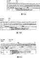
MFC命令使用多个影响命令操作的参数。图3A是示出了根据本发明的示意性实施例的用于MFC命令的参数助记符的示意图。所有命令并不使用所有参数。例如,EAH参数是可选的。当未在命令中指定可选参数时,硬件将可选参数设置为“0”。MFC commands use several parameters that affect the operation of the command. FIG. 3A is a diagram illustrating parameter mnemonics for MFC commands according to an exemplary embodiment of the present invention. Not all commands use all parameters. For example, the EAH parameter is optional. When an optional parameter is not specified in the command, the hardware sets the optional parameter to "0".
MFC命令可以分为三类:定义的命令、非法命令和保留的命令。通过检查操作码以及扩展操作码(如果存在)来确定命令的分类。如果命令操作码或操作码和扩展操作码的组合不是定义的或保留的命令的操作码或操作码和扩展操作码的组合,则命令是非法的。MFC commands can be divided into three categories: defined commands, illegal commands, and reserved commands. The command's classification is determined by examining the opcode and, if present, the extended opcode. A command is illegal if the command opcode or combination of opcode and extended opcode is not that of a defined or reserved command.
定义的命令属于三种类别之一:数据传输命令、SL1高速缓存管理命令和同步命令。数据传输命令进一步分为定义数据移动方向(即到达或来自本地存储)的子类别。Put命令是将数据从本地存储移动到主存储的数据传输命令。Get命令是将数据从主存储移动到本地存储的数据传输命令。应用可以将数据传输命令放置在MFC代理命令队列270中。除非另行说明,否则这些命令可以按任何顺序(异步)执行。The defined commands fall into one of three categories: data transfer commands, SL1 cache management commands, and synchronization commands. Data transfer commands are further divided into subcategories that define the direction of data movement (i.e. to or from local storage). Put commands are data transfer commands that move data from local storage to primary storage. Get commands are data transfer commands that move data from primary storage to local storage. Applications can place data transfer commands in the MFC proxy command queue 270 . These commands can be executed in any order (asynchronously) unless otherwise stated.
“非法”类命令指不在定义的类或保留的类中的命令。“保留”类命令旨在用于与实施方式相关的用途。An "illegal" class command is one that is not in a defined class or a reserved class. Commands of the "reserved" class are intended for implementation-dependent purposes.
SL1存储控制命令是用于控制有关SL1高速缓存的操作的命令。这些存储控制命令例如包括用于通知SL1高速缓存可能要发出特定类型的数据传输命令(例如get或put命令)的“提示”命令、地址范围操作命令和刷新命令。The SL1 storage control command is a command for controlling operations related to the SL1 cache. These storage control commands include, for example, "hint" commands for informing the SL1 cache that a particular type of data transfer command (eg, a get or put command) may be issued, address range manipulation commands, and flush commands.
MFC同步命令用于控制相对于其他MFC、处理器和其他设备来执行存储访问的顺序。MFC同步命令包括用于强制按顺序执行的命令、用于相对于DMA命令队列中位于屏障命令之前的所有命令来排序所有后续命令的屏障命令,以及用于在目标信号通知寄存器中逻辑地设置信号位的发送信号命令等。MFC synchronization commands are used to control the order in which memory accesses are performed relative to other MFCs, processors, and other devices. MFC synchronization commands include commands to enforce in-order execution, barrier commands to order all subsequent commands relative to all commands preceding the barrier command in the DMA command queue, and to logically set the signal in the target signaling register Bit send signal command, etc.
MFC命令可以是单个DMA命令或者可以是DMA列表命令。图3B中示出了根据本发明的示意性实施例的DMA列表命令的详细信息。DMA列表命令使用存储在本地存储中的有效地址和传输大小对的列表或列表元素作为DMA传输的参数。这些参数用于MFC代理命令队列不支持的SPU启动的DMA列表命令。每个列表元素的第一个字包含传输大小以及停止和通知标志。第二个字包含有效地址的低32位。虽然为列表中的每个传输元素指定了开始有效地址,但是主要列表命令中仅指定了传输中涉及的本地存储地址(术语“主要”指由图3A中所示的参数指定的列表命令)。The MFC command can be a single DMA command or can be a DMA list command. Detailed information of a DMA list command according to an exemplary embodiment of the present invention is shown in FIG. 3B. The DMA list command takes a list or list elements of effective address and transfer size pairs stored in local storage as parameters for a DMA transfer. These parameters are used for SPU-initiated DMA list commands that are not supported by the MFC proxy command queue. The first word of each list element contains the transfer size and stop and notify flags. The second word contains the lower 32 bits of the effective address. While a starting effective address is specified for each transfer element in the list, only the local storage addresses involved in the transfer are specified in the main list command (the term "main" refers to the list command specified by the parameters shown in Figure 3A).
本地存储地址根据列表中的每个元素传输的数据量在内部递增。但是,由于对齐限制,如果本地存储地址没有在列表元素传输的16字节边界上开始,则硬件自动将本地存储地址递增到下一个16字节边界。仅当使用小于16字节的传输大小时才会发生此情况。传输大小小于16字节的列表元素在由有效地址的4个最低位定义的当前四倍长字(16字节)内使用本地存储偏移。The local storage address is internally incremented according to the amount of data transferred for each element in the list. However, due to alignment constraints, the hardware automatically increments the local storage address to the next 16-byte boundary if the local storage address does not start on the 16-byte boundary where the list element is transferred. This only happens when using a transfer size smaller than 16 bytes. List elements with a transfer size of less than 16 bytes use a local storage offset within the current quadword (16 bytes) defined by the 4 least significant bits of the effective address.
在列表元素中指定的有效地址是相对于由基本DMA列表命令中指定的有效地址的高32位定义的4GB区域的。虽然DMA列表开始地址是相对于单个4GB区域的,但是列表元素内的传输可以跨4GB边界。The effective address specified in the list element is relative to the 4GB region defined by the upper 32 bits of the effective address specified in the basic DMA list command. Although DMA list start addresses are relative to a single 4GB region, transfers within list elements can cross 4GB boundaries.
设置“S”(停止和通知)位会使DMA操作在当前列表元素已被处理之后挂起此列表的执行,并针对SPU设置停止和通知事件状态。在MFC从SPU程序接收到停止和通知确认之前,已停止的列表不会重新开始执行。使用关联的命令标记组标识符将停止和通知事件发布到SPU程序。当同一标记组中存在多个具有停止和通知元素的DMA列表命令时,软件将确保使用标记特定的屏障或全局屏障来强制有序执行DMA列表命令以免产生不定性。Setting the "S" (stop and notify) bit causes the DMA operation to suspend the execution of this list after the current list element has been processed, and sets the stop and notify event status for the SPU. A stopped list does not restart execution until MFC receives a stop and notify acknowledgment from the SPU program. Post stop and notify events to the SPU program using the associated command tag group identifier. When there are multiple DMA list commands with STOP and NOTIFY elements in the same tag group, software will ensure that tag-specific barriers or global barriers are used to enforce orderly execution of DMA list commands to avoid ambiguity.
将保证DMA列表命令内的所有DMA列表元素都按顺序启动和发出。DMA列表命令内的所有元素都具有固有的本地排序。单个DMA列表命令可以包含最多2048个元素,占用16KB的本地存储。All DMA list elements within a DMA list command will be guaranteed to be initiated and issued in order. All elements within a DMA list command have an inherent local ordering. A single DMA list command can contain up to 2048 elements, occupying 16KB of local storage.
通道接口channel interface
在BPA中,通道用作协处理单元(SPU)和存储器流控制(MFC)单元之间的主要接口。SPU通道访问设备用于配置、保存和恢复SPU通道。SPU指令集体系结构(ISA)提供一组通道指令以便通过通道接口(或SPU通道)与外部设备通信。表1列出了这些指令:In BPA, a channel is used as the main interface between the co-processing unit (SPU) and the memory flow control (MFC) unit. The SPU channel access device is used to configure, save and restore SPU channels. The SPU Instruction Set Architecture (ISA) provides a set of channel instructions to communicate with external devices through a channel interface (or SPU channel). Table 1 lists these directives:
表1-通道指令Table 1-Channel Instructions
在体系结构上,SPU通道可以配置为具有只读或只写的访问类型。通道不能配置为读取和写入。除了访问类型之外,每个通道可以配置为非阻塞或阻塞。配置为阻塞的通道使SPU在读取通道计数为“0”的通道或写入满通道(即,通道计数为“0”的通道)时停止。“读取”通道表示只有读取通道指令(rdch)可以被发出到此通道并始终返回数据。“写入”通道表示只有写入通道指令(wrch)可以被发出到此通道且通道始终接受数据。Architecturally, SPU channels can be configured with read-only or write-only access types. Channels cannot be configured for reading and writing. In addition to the access type, each channel can be configured as non-blocking or blocking. Channels configured as blocked cause the SPU to stall when reading a channel with a channel count of "0" or writing to a full channel (ie, a channel with a channel count of "0"). A "read" channel means that only read channel commands (rdch) can be issued to this channel and always return data. A "write" channel means that only write channel commands (wrch) can be issued to this channel and the channel always accepts data.
“读取阻塞”通道表示只有读取通道指令(rdch)可以被发出到此通道。仅当通道计数不为零时,发送到读取阻塞通道的读取通道指令(rdch)才会完成。通道计数为“0”表示通道为空。对计数为“0”的读取阻塞通道执行通道读取(rdch)会导致SPU停止,直到通道中的数据可用。A "read blocking" channel means that only read channel commands (rdch) can be issued to this channel. A read channel instruction (rdch) sent to a read-blocked channel completes only if the channel count is non-zero. A channel count of "0" indicates that the channel is empty. Performing a channel read (rdch) on a read-blocking channel with a count of "0" causes the SPU to stall until data is available in the channel.
“写入阻塞”通道表示只有写入通道指令(wrch)可以被发出到此通道。仅当通道计数不为零时,发送到写入阻塞通道的写入通道指令(wrch)才会完成。通道计数为“0”表示通道是满的。对计数为“0”的写入阻塞通道执行写入通道指令(wrch)会导致SPU停止,直到已寻址的通道中的表项变得可用。A "write blocking" channel means that only write channel commands (wrch) can be issued to this channel. A write channel command (wrch) sent to a write-blocked channel completes only if the channel count is non-zero. A channel count of "0" indicates that the channel is full. Executing a write channel instruction (wrch) on a write blocking channel with a count of "0" causes the SPU to stall until an entry in the addressed channel becomes available.
应当指出,发出不适用于通道配置的通道指令会导致无效的通道指令中断。例如,向配置为写入或写入阻塞通道的通道发出读取通道指令(rdch)会导致无效的通道指令中断。It should be noted that issuing a channel command that does not apply to the channel configuration will cause an invalid channel command to abort. For example, issuing a read channel command (rdch) to a channel configured as a write or write-blocking channel causes an invalid channel command to abort.
每个通道都具有相应的计数(即,深度),所述计数表示可以针对此通道发出的未完成操作的数量。通道深度(即,未完成传输的最大数量)与实施方式相关。当在SPU中建立新的上下文时,或者继续现有上下文时,软件必须初始化通道计数。Each channel has a corresponding count (ie, depth) that represents the number of outstanding operations that can be issued against this channel. The channel depth (ie, the maximum number of outstanding transfers) is implementation dependent. When establishing a new context in the SPU, or when continuing an existing context, software must initialize the channel count.
在标题为“External Message Passing Method and Apparatus”(申请日为2003年6月26日,在此引入作为参考)的共同未决和共同受让的美国专利申请公开No.2004/0264445中说明了通道和通道接口的操作。图4是示出了根据美国专利申请公开No.2004/0264445中所述机制的关于单对通道的通道电路的SPU发出和控制逻辑以及数据流的布置的示意图。现在将参考图4中示出的各个方块来描述通道接口的操作。Channels are described in co-pending and commonly assigned U.S. Patent Application Publication No. 2004/0264445, entitled "External Message Passing Method and Apparatus," filed June 26, 2003, incorporated herein by reference. and channel interface operations. 4 is a schematic diagram illustrating the arrangement of SPU issue and control logic and data flow for channel circuits of a single pair of channels according to the mechanism described in US Patent Application Publication No. 2004/0264445. The operation of the channel interface will now be described with reference to the various blocks shown in FIG. 4 .
如图4所示,方块430表示SPU的外部设备指令发出和控制逻辑。方块432表示到达和来自SPU的数据流。如所公知的,处理器可以同时与许多不同的外部设备通信。在现在的处理器中,通过通道寄存器完成通信。每个通道仅在一个方向上工作,并且根据SPU可以对通道执行的操作而称为读取通道或写入通道。方块434表示由方块435表示的单个外部设备的一组通道的通道逻辑。如将在以下更详细讨论的,此外部设备435可以是MFC(例如MFC 200)、机器状态寄存器或任何其他类型的外部设备。具体地说,在通道接口的此一般描述之后,将在其后描述使用通道接口与MFC、机器状态寄存器、事件设备、邮箱设备以及信号通知设备进行通信。As shown in FIG. 4, block 430 represents the SPU's external device command issuing and control logic.
在方块434内,示出了读取通道计数器436、读取寄存器438、写入通道计数器440、写入寄存器442、MUX(多路复用器)444和MUX 446。通道指令在总线448上从SPU发出和控制逻辑430传递到读取计数器和写入计数器436和440以及传递到MUX 444和446的门输入。这些指令还在通道输出线450上提供给相应的外部设备(例如435)。数据输入线452将数据从外部设备435提供给读取寄存器438。通道计数输入信号在通道输入线454上从外部设备435提供给计数器436,表示数据已输入到寄存器并运行以便以单位值或单个位来改变计数器436中的计数。Within
在数据输出线456上提供要从写入寄存器442输出到外部设备435的数据。当外部设备435已完成满意的数据接收并运行以便以单位值或单个位来改变计数器440中的计数时,通道确认信号在通道确认线458上从外部设备435返回写入通道计数器440。在本发明的优选实施例中,总线448上的信号将递减相应读取计数器或写入计数器的计数,而线454或458上的信号将递增相应读取计数器或写入计数器的计数。Data to be output from
如所示出的,计数器436和440的计数在通道停止线460上通过MUX444提供给SPU发出和控制逻辑430。通道写入数据在通道写入数据线462上从SPU数据流方块432提供给写入寄存器442。来自方块436、438和440的输出在总线464上返回数据流方块432。非通道指令通过总线466在方块430和432之间传送。As shown, the counts of
图5提供了示出根据本发明的示意性实施例的通道接口的示意性操作的流程图。将理解的是,图5中的流程图以及此后描述的后续图中的流程图的每个方块以及方块组合可以通过计算机程序指令实现。可以向处理器或其他可编程数据处理装置提供这些计算机程序指令以产生机器,以使在所述处理器或其他可编程数据处理装置上执行的指令创建用于实现一个或多个流程图方块中指定的功能的装置。这些计算机程序指令还可以存储在引导处理器或其他可编程数据处理装置以特定方式运行的计算机可读存储器或存储介质中,以使存储在计算机可读存储器或存储介质中的指令生成包括实现一个或多个流程图方块中指定的功能的指令装置的制品。FIG. 5 provides a flowchart illustrating exemplary operation of a channel interface according to an exemplary embodiment of the present invention. It will be understood that each block, and combinations of blocks, of the flowchart in FIG. 5 , and the flowcharts in subsequent figures described thereafter, can be implemented by computer program instructions. These computer program instructions may be provided to a processor or other programmable data processing apparatus to produce a machine, such that the instructions executed on said processor or other programmable data processing apparatus create a process for implementing one or more of the flow chart blocks. device for the specified function. These computer program instructions may also be stored in a computer-readable memory or storage medium that directs a processor or other programmable data processing device to operate in a specific manner, such that generating instructions stored in the computer-readable memory or storage medium includes implementing a or an article of manufacture of instruction means for the functions specified in a plurality of flowchart blocks.
相应地,流程图的方块支持用于执行指定功能的装置组合、用于执行指定功能的步骤组合,以及用于执行指定功能的程序指令装置。还将理解的是,流程图的每个方块以及流程图中的方块组合可以通过执行指定功能或步骤的基于专用硬件的计算机系统来实现,或者通过专用硬件和计算机指令的组合来实现。Accordingly, blocks of the flowchart support combinations of means for performing the specified functions, combinations of steps for performing the specified functions and program instruction means for performing the specified functions. It will also be understood that each block of the flowchart illustrations, and combinations of blocks in the flowchart illustrations, can be implemented by special purpose hardware-based computer systems which perform the specified functions or steps, or combinations of special purpose hardware and computer instructions.
如图5所示,通道读取或写入指令的发出将导致判定指定的通道是否为已经实现如上所述的控制机制的通道(步骤576)。如果否,则判定是否启用了通道错误逻辑(步骤578)。如果启用,则处理器将停止(步骤580)。如果未启用,则判定命令是读取命令还是写入命令(步骤582)。As shown in FIG. 5, the issuance of a channel read or write command will result in a determination of whether the specified channel is one that has implemented the control mechanism described above (step 576). If not, it is determined whether the channel error logic is enabled (step 578). If enabled, the processor will stall (step 580). If not enabled, it is determined whether the command is a read command or a write command (step 582).
如果未实现的命令是写入命令,则不会针对此命令进一步执行任何操作(步骤584)。另一方面,如果未实现的命令是读取命令,则向数据处理器数据流返回零(步骤586)。在这两种情况下,过程都将返回到等待下一个读取或写入指令的状态。在示出的优选实施例中,所有有效的读取指令都必须返回值。如在此定义的,到未实现的通道的通道读取指令将返回均为零的值。If the unimplemented command is a write command, no further operations are performed on this command (step 584). On the other hand, if the unimplemented command is a read command, then zero is returned to the data processor stream (step 586). In both cases, the process returns to waiting for the next read or write instruction. In the preferred embodiment shown, all valid read instructions must return a value. A channel read instruction to an unimplemented channel will return a value of all zeros, as defined herein.
要指出的是,对于特定实施方式,并非必须定义所有通道。每个通道将具有唯一的数字标识符。在优选实施例中,此通道标识符的范围为0到127。但是,因为不需要定义所有通道,所以可能不会使用所有标识符。因此,如果有一个到未定义通道的指令,则过程将沿上面引用的未实现路径继续。在某些实施方式中,可能需要将到未实现通道的通道读取或写入命令视为非法操作。进一步的操作可能是强制处理器停止,如上述步骤580中所示。It is to be noted that not all channels have to be defined for a particular implementation. Each channel will have a unique numeric identifier. In a preferred embodiment, this channel identifier ranges from 0 to 127. However, because not all channels need to be defined, not all identifiers may be used. Therefore, if there is an instruction to an undefined channel, the process will continue along the unimplemented path referenced above. In some implementations, it may be desirable to treat a channel read or write command to an unimplemented channel as an illegal operation. A further action may be to force the processor to stop, as shown in
返回图5,如果在步骤576中判定已经实现指定的通道,则进行检查以查看指定的通道是否为阻塞通道(步骤588)。如果否,则递减此通道的计数,但不允许小于零(步骤590)。如果判定通道为阻塞通道,则进行检查以确定此通道的计数是否大于零(步骤592)。如果是,则过程返回步骤590。Returning to Figure 5, if it is determined in
如果计数已经为零,如在步骤592中判定的那样,则SPU停止,直到外部设备提供与此通道相关的输入并且因此从零更改计数(步骤594和595)。因此,将定期处理步骤594和595的循环,直到此通道的计数发生更改。一旦计数更改,过程将从步骤595继续到步骤590。If the count is already zero, as determined in
此后,将判定通道是主动的还是被动的(步骤596)。如果通道是被动的,则进行检查以查看命令是写入指令还是读取指令(步骤598)。如果命令是写入指令,则将数据存储在本地以供外部读取(步骤600)。如果命令是读取指令,则通过图4的SPU数据流432将数据返回SPU(步骤602)。Thereafter, it will be determined whether the channel is active or passive (step 596). If the channel is passive, a check is made to see if the command is a write command or a read command (step 598). If the command is a write instruction, then store the data locally for external reading (step 600). If the command is a read instruction, the data is returned to the SPU via the
应当指出的是,在被动通道的情况下,SPU依赖于外部过程来完成操作。作为一个实例,读取通道可以依赖于外部设备来加载数据。另一方面,在主动通道中,SPU主动地完成执行读取或写入操作的操作。连接的硬件针对主动读取通道中的数据发出外部请求是此类型操作的一个实例。It should be noted that in the case of passive channels, the SPU relies on external processes to complete operations. As an example, read channels may rely on external devices to load data. In an active channel, on the other hand, the SPU actively completes the operation performing a read or write operation. Connected hardware making an external request to actively read data from a channel is an example of this type of operation.
当在步骤596中判定通道是主动通道时,将进行检查以查看命令是读取命令还是写入命令(步骤604)。如果命令是写入命令,则将写入数据向外输出到SPU或内部寄存器(步骤606)。如果命令是读取命令,则将读取请求发送到相应的外部设备(步骤608)。When it is determined in
将等待请求数据的输入(步骤610)。将定期地判定是否已接收到读取数据(步骤612)。如果否,则过程返回步骤610,直到进行下次检查时。当接收到数据时,过程完成(步骤602)。Input of request data will be awaited (step 610). It will be periodically determined whether read data has been received (step 612). If not, the process returns to step 610 until the next check. When data is received, the process is complete (step 602).
根据上述内容,使用特定的通道读取或写入指令(其中在指令中指定了通道号)访问每个通道将是显而易见的。每个通道都具有为其指定的计数。此计数使用读取通道计数指令(其中在指令中指定了感兴趣的通道)来读取。通道命令不是推测性的,并且不能在外部接口处被乱序处理。通道体系结构不要求SPU外部的设备按顺序处理通道命令,但是可能会根据处理器和外部设备实施方式而执行此操作。此计数寄存器中的值将跟踪对此寄存器的访问次数与已针对此寄存器发生的外部确认次数。From the above, it will be apparent that each channel is accessed using a specific channel read or write command (where the channel number is specified in the command). Each channel has a count assigned to it. This count is read using the read channel count instruction where the channel of interest is specified in the instruction. Channel commands are not speculative and cannot be processed out of order at the external interface. The channel architecture does not require devices external to the SPU to process channel commands sequentially, but may do so depending on the processor and peripheral implementation. The value in this count register will keep track of the number of accesses to this register and the number of external acknowledgments that have occurred for this register.
在操作中,经由通过外部接口(多个)的访问更改通道计数的方式是基于实施方式的。在优选实施例中,对于每个到达或来自寄存器的成功数据传输,计数以1为单位递增。对于每个通道,SPU访问可以被定义为读取或写入通道。进而,在优选实施例中,当通道被定义或实现为“阻塞”通道时,使用“0”计数停止进一步的操作。当通道寄存器定义为具有为“1”的队列深度时,“0”计数可以用于指示此通道中的数据无效。通道还可以定义为停止在读取或写入通道命令时的SPU操作(在此命令时,如果计数为“0”),直到计数不再为“0”。In operation, the manner in which the lane count is changed via access through the external interface(s) is implementation-dependent. In a preferred embodiment, the count is incremented by 1 for each successful data transfer to or from the register. For each channel, SPU access can be defined as reading or writing to the channel. Furthermore, in a preferred embodiment, when a channel is defined or implemented as a "blocking" channel, a "0" count is used to stop further operations. When a channel register is defined to have a queue depth of "1", a "0" count can be used to indicate that the data in this channel is invalid. A channel can also be defined to stop SPU operation on a read or write channel command (if the count is "0" at the time of this command), until the count is no longer "0".
在优选实施例中,对于每个SPU启动的读取或写入通道命令,计数器值递减,对于每个外部启动的读取或写入(带有或不带有数据)访问,计数器值递增。换言之,计数器保持输入与输出的指示。因此,对于写入,为“0”的值或计数指示没有更多的外部写入槽可用。另一方面,对于读取,为“0”的计数值指示没有有效的数据。当计数为零时,如果发出其他SPU读取或写入通道命令,并且通道定义为非阻塞,则计数将保持为“0”并且寄存器中的数据将丢失。如优选实施例中实现的,此寄存器中的先前最新数据将丢失。如果对于此通道寄存器实施方式的位数,计数处于最大值,并且发生其他将导致计数超范围递增的事务,则计数将停留在此最大值。In a preferred embodiment, the counter value is decremented for each SPU initiated read or write channel command and incremented for each externally initiated read or write (with or without data) access. In other words, the counter keeps an indication of inputs and outputs. Thus, for writes, a value or count of "0" indicates that no more external write slots are available. On the other hand, for reading, a count value of "0" indicates that there is no valid data. When the count is zero, if another SPU read or write channel command is issued, and the channel is defined as non-blocking, the count will remain at "0" and the data in the register will be lost. As implemented in the preferred embodiment, the previous latest data in this register will be lost. If the count is at its maximum value for the number of bits implemented by this channel register, and other transactions occur that would cause the count to be incremented out of range, the count will stay at this maximum value.
初始化计数值的方法与实施方式相关,并且一种方法是通过外部接口进行初始化。此计数可用于写入队列的流控制。可以将计数预先设置为外部队列的深度。计数寄存器中的零值表示此外部队列中没有更多的空间。对于为“1”的外部队列深度,计数应预先设置为“1”。当SPU写入此通道时,计数将转到“0”。当外部设备从此通道中读取时,计数将递增到“1”,由此指示通道已准备好其他写入操作。A method of initializing the count value is implementation-dependent, and one method is initialization through an external interface. This count can be used for flow control of write queues. The count can be preset to the depth of the external queue. A value of zero in the count register indicates that there is no more room in this external queue. For an external queue depth of "1", the count shall be pre-set to "1". When the SPU writes to this channel, the count will go to "0". When an external device reads from this channel, the count is incremented to '1', thereby indicating that the channel is ready for another write operation.
如上所述,对于通道寄存器的读取,这允许计数指示有效数据。如果计数寄存器预先设置为“0”,这指示数据无效。当外部设备向此通道写入时,计数将递增到“1”,指示数据对于SPU读取有效。当SPU从此通道中读取时,计数将递减回“0”,指示可以发生其他外部写入。As mentioned above, for channel register reads, this allows the count to indicate valid data. If the count register is previously set to "0", this indicates that the data is invalid. When an external device writes to this channel, the count will increment to "1", indicating that the data is valid for the SPU to read. When the SPU reads from this channel, the count will decrement back to "0", indicating that additional external writes can occur.
在本发明的优选实施例中,计算机代码通道计数读取指令被发送到计数器以确定读取和写入通道的计数。当外部设备为智能设备(例如多处理器环境中的其他SPU或计算设备)时,外部设备还可以将通道计数读取指令发送到计数器以确定计数。通过此方式,外部设备可以确定通道何时在读取或写入通道中包含未读取的数据和/或何时适于将其他数据发送到包含读取通道的处理器。In a preferred embodiment of the invention, computer code channel count read instructions are sent to the counters to determine the counts for the read and write channels. When the external device is an intelligent device (such as other SPUs or computing devices in a multi-processor environment), the external device can also send a channel count read instruction to the counter to determine the count. In this way, the external device can determine when a channel contains unread data in a read or write channel and/or when it is appropriate to send additional data to the processor containing the read channel.
使用本发明,读取和写入通道可以为非累积或累积的。累积通道是累积多个写入的通道。即,将入站数据逻辑地添加到已包含在寄存器或其他存储装置中的数据,直到读取该通道。读取该通道时,通常将累积寄存器重置为“0”,并且通道将再次开始累积。此操作可以用于读取或写入通道。Using the present invention, read and write channels can be non-cumulative or cumulative. A cumulative channel is a channel that accumulates multiple writes. That is, the inbound data is logically added to the data already contained in registers or other storage until the channel is read. When the channel is read, the accumulation register is usually reset to "0" and the channel will start accumulating again. This operation can be used to read or write to the channel.
进而,累积通道可以为阻塞或非阻塞的。通常,累积通道将仅具有为“1”的计数深度,而非累积通道可用于对向此通道执行的每个写入计数。Furthermore, accumulation channels can be blocking or non-blocking. Typically, an accumulative channel will only have a count depth of "1", while a non-accumulative channel can be used to count every write performed to this channel.
概括地说,通道接口使用已定义的通道来释放存储器,但仍提供有关寄存器中的数据何时有效(换言之,先前尚未被读取)的易于访问的信息。通过向计数机制发送通道计数读取指令来获取此信息。当智能外部设备连接到给定通道时,外部设备可以使用类似指令向给定通道发送数据或从给定通道接收数据。当指定的通道定义为非阻塞通道时,通道接口还可通过使用通道计数读取指令进一步防止意外覆盖寄存器中的数据。In a nutshell, a channel interface uses a defined channel to free memory but still provide easily accessible information about when data in a register is valid (in other words, has not been previously read). This information is obtained by sending a channel count read command to the counting mechanism. When an intelligent peripheral is connected to a given channel, the peripheral can use similar commands to send data to or receive data from the given channel. The channel interface also further prevents accidental overwriting of data in registers by using channel count read instructions when the specified channel is defined as a non-blocking channel.
本发明使用通道接口和已定义的通道来向/从不同类型的外部设备以及由此类外部设备提供的设备传送指令和数据。例如,本发明提供了用于使用SPU的通道接口与MFC、机器状态寄存器和中断设备传送指令和数据的机制。此外,通道接口用于与BPA的事件设备、邮箱设备、多源同步设备、代理标记组完成设备、信号通知设备等传送指令和数据。The present invention uses a channel interface and defined channels to transfer instructions and data to and from different types of external devices and devices provided by such external devices. For example, the present invention provides mechanisms for communicating instructions and data with the MFC, machine status registers, and interrupt devices using the SPU's channel interface. In addition, the channel interface is used to transmit instructions and data with BPA's event device, mailbox device, multi-source synchronization device, agent mark group completion device, signal notification device, etc.
图6A是示出了本发明的一个实施例使用通道的方式的示意图。如图6A所示,通道接口620提供多个通道,SPU 622可以通过这些通道与MFC624、机器状态寄存器634和中断设备636通信。每个通道可以包括类似于上面图4中所述元素的元素,并且其操作类似于图5A和5B中所述的操作。在本发明的一个示意性实施例中,通道接口620可以对应于由图4中的方块434表示的所有通道对的聚合。SPU 622可以对应于图4中的方块430和432的组合,例如,图6中的其他所有方块对应于图4中的方块435。Figure 6A is a schematic diagram illustrating the manner in which channels are used by one embodiment of the present invention. As shown in FIG. 6A, the
如图6A所示,通道631、633和635提供与SPU 622关联的通信路径,SPU事件设备630和递减器632可以通过此路径与MFC 624通信。SPU事件设备630提供用于处理在BPA内生成的事件的机制。通道633提供用于标识感兴趣事件以及获取有关这些感兴趣事件的信息的机制,如将在以下更详细讨论的。递减器632提供了SPU上运行的软件可以借助其测量时间进度或被通知经过的给定测量时间的机制。递减器632可以通过通道631设置其值以及读取状态。As shown in FIG. 6A,
SPU(发出和控制逻辑、处理器数据流)622提供用于与外部设备通信的指令、数据和设备。例如,SPU 622提供了SPU通道访问设备,此设备是初始化、保存和恢复SPU通道的特权设备。所述设备包括三个MMIO寄存器:SPU通道索引寄存器、SPU通道计数寄存器和SPU通道数据寄存器。SPU通道索引寄存器是指向其计数和数据分别由SPU通道计数寄存器和SPU通道数据寄存器访问的通道的指针。SPU通道索引寄存器选择使用SPU通道计数寄存器或SPU通道数据寄存器访问的SPU通道。SPU通道数据寄存器用于读取或初始化由SPU通道索引寄存器选择的SPU通道数据。SPU (issue and control logic, processor data flow) 622 provides instructions, data and facilities for communicating with external devices. For example,
除了用于与SPU 622的设备通信的通道631、633和635之外,通道637提供了与机器状态寄存器634关联的通信路径。机器状态寄存器634包含当前机器隔离状态和中断状态。隔离状态指示是否已将SPU隔离。BPA的隔离设备使得特权软件和应用能够将代码映像隔离和加载到一个或多个SPU中。SPU隔离设备确保加载到关联的SPU本地存储的代码映像尚未被任何装置改变。当支持嵌套的中断时,与中断状态相关的机器状态寄存器用于保存和恢复中断状态信息。
此外,通道639提供与中断设备636关联的通信路径。中断设备636用于将中断和中断状态信息路由到PPE或外部设备、将提供给PPE的中断按照优先顺序排序,并生成处理器间中断。Additionally,
此外,通道641提供与邮箱设备638关联的通信路径。邮箱设备638用于将信息发送到外部设备(例如其他SPU、PPE等)或用于从其接收信息。Additionally,
通道643提供与SPU信号通知设备640关联的通信路径。SPU信号通知设备640用于将信号(例如缓冲区完成标志)从系统中的其他处理器和设备发送到SPU。
通道645提供与代理标记组完成设备642关联的通信路径。代理标记组完成设备642是用于确定何时完成一组类似标记指令的处理的设备。
通道647提供与MFC多源同步设备644关联的通信路径。MFC多源同步设备644实现跨本地存储和主存储地址域的累积排序。由多个源(即,两个或更多个处理器或单元)相对于其他处理器或单元执行的存储访问的排序被称为累积排序。
图6B和6C示出了根据本发明的一个示意性实施例的列出SPU通道图的示意图。如图6所示,SPU通道接口支持各种类型的用于传送指令和数据的通道。这些通道包括SPU事件通道650、SPU信号通知通道652、SPU递减器通道654、MFC多源同步通道656、SPU保留通道658、掩码读取通道660、SPU状态管理通道662、MFC命令参数通道664、MFC标记状态通道666以及SPU邮箱通道668。这些“通道”本质上是存储器映射的寄存器以及用于写入这些寄存器的相应电路。因此,术语“通道”在此还可以用于指存储与指定的“通道”对应的数据值的一个或多个寄存器。将在以下描述这些通道中的每个通道的操作。在PPE、SPU和MFC中提供了各种用于使用这些通道的设备。将在以下详细描述这些类型的通道中的每种通道,从用于与MFC通信的这些通道开始。6B and 6C show schematic diagrams listing SPU channel maps according to an exemplary embodiment of the present invention. As shown in Figure 6, the SPU channel interface supports various types of channels for transferring instructions and data. These channels include
MFC命令参数通道MFC command parameter channel
MFC命令参数通道664是用于将数据写入MFC SPU命令队列的MFC命令参数寄存器的通道(参见以上的图2和表1)。MFC命令参数通道664是非阻塞的并且没有与其关联的通道计数。因此,执行发送到这些通道中的任何通道的读取通道计数(rchcnt)指令将返回计数“1”。The MFC
MFC命令参数通道664包括MFC本地存储地址通道、MFC有效高地址通道、MFC有效低地址或列表地址通道、MFC传输大小或列表大小通道、MFC命令标记标识通道、MFC命令操作码通道以及MFC类ID通道。将在以下详细描述这些通道中的每个通道。MFC
MFC命令操作码通道MFC command opcode channel
图7A中提供了根据本发明的一个示意性实施例的MFC命令操作码通道的详细信息。MFC命令操作码通道根据操作码标识要执行的操作。将相对于指令流异步地检查此操作码的有效性。如果MFC命令或任何命令参数无效,则MFC命令队列处理将挂起并生成无效的MFC命令中断。Detailed information of the MFC command opcode channel according to an exemplary embodiment of the present invention is provided in FIG. 7A . The MFC command opcode channel identifies the operation to perform based on the opcode. The validity of this opcode will be checked asynchronously with respect to the instruction stream. If the MFC command or any command parameters are invalid, MFC command queue processing will hang and generate an invalid MFC command interrupt.
使用单个通道指令将MFC命令和类ID参数写入MFC SPU命令队列。如图7A所示,在优选实施例中,MFC命令操作码参数是32位字的低16位。此字段的高8位被保留,低8位标识了MFC命令操作码。Writes MFC command and class ID parameters to the MFC SPU command queue using a single channel instruction. As shown in FIG. 7A, in the preferred embodiment, the MFC command opcode parameter is the lower 16 bits of a 32-bit word. The upper 8 bits of this field are reserved, and the lower 8 bits identify the MFC command opcode.
MFC类ID通道MFC class ID channel
MFC类ID通道用于指定每个MFC命令的替换类ID和传输类ID,如图7B所示。SPU和软件使用这些ID来提高系统的整体性能。具体地说,替换类ID(RclassID)与替换管理表(RMT)一起使用以控制高速缓存替换。可以例如从PPE操作的加载和存储地址来生成替换类ID(PPE包括地址范围设备,此设备提供了一种将用于PPE加载和存储以及指令取回的有效地址或实地址映射到高速缓存替换管理设备的类ID的方法)。The MFC class ID channel is used to specify the replacement class ID and transport class ID of each MFC command, as shown in FIG. 7B. The SPU and software use these IDs to improve the overall performance of the system. Specifically, the replacement class ID (RclassID) is used with the replacement management table (RMT) to control cache replacement. The replacement class ID can be generated, for example, from the load and store addresses of PPE operations (PPEs include address range facilities that provide a way to map effective or real addresses for PPE loads and stores and instruction fetches to cache replacement method to manage the class ID of the device).
RclassID用于生成用于控制替换策略的特权软件管理的表(即替换管理表(RMT))的索引。RMT的格式与实施方式相关。RMT包括数量与实施方式相关的表项,这些表项应包含成组启用位、有效位以及其他控制信息。可选地,一种实施方式还可以提供高速缓存旁路位和算法位。RMT表中的表项数以及每个表项的大小与实施方式相关。RclassID is used to generate an index to a privileged software-managed table for controlling replacement policies, the Replacement Management Table (RMT). The format of the RMT is implementation dependent. The RMT includes an implementation-dependent number of entries that shall contain group enable bits, valid bits, and other control information. Optionally, an embodiment may also provide cache bypass bits and algorithm bits. The number of entries in the RMT table and the size of each entry are related to the implementation.
图7C示出了用于8路、成组相联高速缓存的典型RMT表项。RMT表位于系统的实地址空间中。特权软件应将这些RMT表映射为特权页。一种实施方式应为每个主要的高速缓存结构提供RMT。Figure 7C shows a typical RMT entry for an 8-way, set associative cache. The RMT table is located in the real address space of the system. Privileged software should map these RMT tables as privileged pages. An implementation should provide an RMT for each major cache structure.
返回图7B,传输类ID(TclassID)用于标识对具有不同特征的存储的访问。TclassID旨在用于允许实施方式根据存储位置的特征来优化对应于MFC命令的传输。TclassID的设置和使用与实施方式相关。Returning to Figure 7B, the transport class ID (TclassID) is used to identify access to storage with different characteristics. TclassID is intended to allow an embodiment to optimize transfers corresponding to MFC commands based on characteristics of storage locations. The setting and use of TclassID are related to the implementation.
RclassID和TclassID(此后称为“类ID参数”)的内容不是永久性的,并且必须针对每个MFC命令入队序列写入。无论与从PPE还是从SPU命令队列的SPU侧发出的命令一起使用,类ID参数都执行相同的功能。类ID参数用于控制与SPE关联的资源,并且对与其他SPE或PPE关联的资源没有任何影响。不会验证类ID参数的有效性。所支持的类ID参数的数量与实施方式相关。The contents of RclassID and TclassID (hereafter referred to as the "class ID parameter") are not persistent and must be written for each MFC command enqueuing sequence. The class ID parameter performs the same function whether used with commands issued from the PPE or from the SPU side of the SPU command queue. The Class ID parameter is used to control the resources associated with the SPE and has no effect on resources associated with other SPEs or PPEs. The validity of the class ID parameter will not be verified. The number of supported class ID parameters is implementation dependent.
MFC命令标记标识通道MFC command tag identifies channel
MFC命令标记标识通道用于为每个命令或一组命令指定标识符。图7D示出了MFC命令标记标识通道的详细信息。例如,标识标记是x′0′与x′1F′之间的任何值。标识标记在硬件中具有纯本地范围。因此,可以在不同的SPE或PPE中使用同一标记。The MFC Command Tag Identification channel is used to specify an identifier for each command or group of commands. FIG. 7D shows the detailed information of the MFC command tag identification channel. For example, the identification flag is any value between x'0' and x'1F'. Identification tags have a purely local scope in hardware. Therefore, the same marker can be used in different SPEs or PPEs.
可以使用同一标识来标记任何数量的MFC命令。使用同一标识标记的MFC命令被称为标记组。标记与写入特定队列的命令关联。提供给MFC SPU命令队列的标记独立于提供给MFC代理命令队列的标记。MFC命令标记标识参数的内容不是永久性的,并且必须针对每个MFC命令入队序列写入。将相对于指令流异步地检查此参数的有效性。如果高位(例如位0到10)没有设置为0,则MFC命令队列处理被挂起并将生成中断。Any number of MFC commands can be marked with the same identifier. MFC commands marked with the same identifier are called a set of tags. Tags are associated with commands written to a particular queue. The flags supplied to the MFC SPU command queue are independent of the flags supplied to the MFC proxy command queue. The contents of the MFC command tag identification parameter are not persistent and must be written for each MFC command enqueuing sequence. The validity of this parameter will be checked asynchronously with respect to the instruction stream. If the upper bits (eg,
MFC传输大小或列表大小通道MFC transfer size or list size channel
MFC传输大小或列表大小通道用于指定MFC传输的大小或MFC DMA传输列表(即一系列DMA传输命令的列表)的大小。图7E中提供了MFC传输大小或列表大小通道的详细信息。在示意性实施例中,传输大小可以具有值1、2、4、8、16或16字节的倍数,最大值为16KB。MFC DMA传输列表大小可以具有值8或8的倍数,最大值为16KB。MFC传输大小或列表大小通道的内容不是永久性的,并且必须针对每个MFC命令入队序列写入。将相对于指令流异步地检查此参数的有效性。如果大小无效,则MFC命令队列处理被挂起并将生成MFC DMA对齐中断。The MFC transfer size or list size channel is used to specify the size of the MFC transfer or the size of the MFC DMA transfer list (that is, a list of a series of DMA transfer commands). Details of the MFC transfer size or list size channels are provided in Figure 7E. In an exemplary embodiment, the transfer size may have values in multiples of 1, 2, 4, 8, 16, or 16 bytes, with a maximum value of 16KB. The MFC DMA transfer list size can have a value of 8 or multiples of 8, with a maximum value of 16KB. The contents of an MFC transfer-size or list-size channel are not persistent and must be written for each MFC command enqueuing sequence. The validity of this parameter will be checked asynchronously with respect to the instruction stream. If the size is invalid, MFC command queue processing is suspended and an MFC DMA alignment interrupt will be generated.
MFC本地存储地址通道MFC local storage address channel
MFC本地存储地址通道用于提供与要排队的MFC命令关联的SPU本地存储地址。MFC本地存储地址用作MFC传输的源或目的地,如MFC命令中所定义的。图7F中提供了MFC本地存储地址通道的详细信息。The MFC local storage address channel is used to provide the SPU local storage address associated with the MFC command to be queued. MFC local storage addresses are used as sources or destinations for MFC transfers, as defined in MFC commands. Details of the MFC local storage address channel are provided in Figure 7F.
MFC本地存储地址通道的内容不是永久性的,并且必须针对每个MFC命令入队序列写入。将相对于指令流异步地检查MFC本地存储地址参数的有效性。如果地址未对齐,则MFC命令队列处理被挂起并将生成MFC DMA对齐异常。例如,为了被看作对齐,本地存储地址的4个最低位必须与有效地址的最低的4个位相匹配。The contents of the MFC local storage address channel are not persistent and must be written for each MFC command enqueuing sequence. The validity of the MFC local storage address parameter will be checked asynchronously with respect to the instruction stream. If the address is not aligned, MFC command queue processing is suspended and an MFC DMA alignment exception will be generated. For example, to be considered aligned, the 4 least significant bits of a local storage address must match the 4 least significant bits of an effective address.
MFC有效低地址或列表地址通道MFC effective low address or list address channel
MFC有效低地址或列表地址通道用于为MFC命令或指向MFC DMA列表命令的列表元素的本地存储指针指定有效低地址。如果在MFC状态寄存器中启用转换,则PPE的地址转换设备将有效地址转换为实地址。图7G提供了MFC有效低地址或列表地址通道的详细信息。The MFC effective low address or list address channel is used to specify the effective low address for an MFC command or a local storage pointer pointing to a list element of an MFC DMA list command. The PPE's address translation facility translates effective addresses to real addresses if translation is enabled in the MFC status register. Figure 7G provides details of MFC's effective low-address or list-address channels.
MFC有效低地址或列表地址通道的内容不是永久性的,并且必须针对每个MFC命令入队序列写入。对于小于16字节的传输大小,此参数的位28到31必须根据传输大小提供自然对齐。对于等于或大于16字节的传输大小,位28到31必须为“0”。如果禁用转换,此参数必须在主存储域的实地址空间限制内。对于MFC列表命令,列表地址的位29到31必须为“0”。如果没有满足这些条件中的任一条件,则参数无效并被视为未对齐。The contents of the MFC effective low address or list address channels are not persistent and must be written for each MFC command enqueuing sequence. For transfer sizes smaller than 16 bytes,
将相对于指令流异步地检查MFC有效低地址或列表地址参数的有效性。如果地址无效,例如由于段错误、映射错误、保护违反或因为地址未对齐,则MFC命令队列处理被挂起并将生成中断。可以生成的中断的类型包括MFC数据段中断、MFC数据存储中断和DMA对齐中断。The validity of the MFC valid low address or list address parameters will be checked asynchronously with respect to the instruction stream. If the address is invalid, for example due to a segmentation fault, mapping fault, protection violation or because the address is misaligned, MFC command queue processing is suspended and an interrupt will be generated. The types of interrupts that can be generated include MFC data segment interrupts, MFC data storage interrupts, and DMA alignment interrupts.
MFC有效高地址通道MFC Active High Address Channel
MFC有效高地址通道用于指定MFC命令的有效地址。如果在MFC状态寄存器中启用转换,则地址转换设备将有效地址转换为实地址。图7H示出了MFC有效高地址通道的详细信息。The MFC effective high address channel is used to specify the effective address of the MFC command. The address translation facility translates effective addresses to real addresses if translation is enabled in the MFC status register. FIG. 7H shows the detailed information of MFC effective high address channel.
MFC有效高地址通道的内容不是永久性的,并且必须针对每个MFC命令入队序列写入。如果没有写入高32位,则硬件设置EAH,高地址位被设置为0,即地址位于0和4GB之间。将相对于指令流异步地检查此参数的有效性。如果地址无效,例如由于段错误、映射错误或保护违反,则MFC命令队列处理被挂起并将生成中断。可以生成的中断的类型包括MFC数据段中断和MFC数据存储中断。应当指出,将在传输过程中检查有效地址的有效性。可以在遇到无效地址并生成异常之前执行部分传输。The contents of the MFC effective high address channel are not persistent and must be written for each MFC command enqueuing sequence. If the upper 32 bits are not written, the hardware sets EAH, and the upper address bit is set to 0, that is, the address is between 0 and 4GB. The validity of this parameter will be checked asynchronously with respect to the instruction stream. If the address is invalid, for example due to a segmentation fault, mapping fault, or protection violation, MFC command queue processing is suspended and an interrupt will be generated. The types of interrupts that can be generated include MFC data segment interrupts and MFC data storage interrupts. It should be noted that valid addresses are checked for validity during transmission. A partial transfer can be performed before an invalid address is encountered and an exception is generated.
使用上述MFC命令参数通道从SPU排队MFC命令时,必须首先将MFC命令参数写入MFC命令参数通道。这可以按任何顺序执行,但MFC命令操作码和类ID参数必须最后写入。因此,为了写入MFC命令参数,将执行图8中示出的操作。When queuing an MFC command from the SPU using the MFC command parameter channel described above, the MFC command parameter must first be written to the MFC command parameter channel. This can be done in any order, but the MFC command opcode and class ID parameters must be written last. Therefore, in order to write the MFC command parameter, the operation shown in FIG. 8 will be performed.
如图8所示,所述操作包括将本地存储地址参数写入MFC本地存储地址通道(步骤810)。将有效高地址参数写入MFC有效高地址通道(步骤820)。将有效低地址或列表地址参数写入MFC有效低或列表地址通道(步骤830)。将MFC传输或列表大小参数写入MFC传输大小或列表大小通道(步骤840)。将MFC命令标记参数写入MFC命令标记标识符通道(步骤850)。在将上述所有参数都写入其各自的通道之后,将MFC命令操作码和类ID参数写入MFC操作码和MFC类ID通道(步骤860),然后操作结束。应当理解,步骤810-850可以按任何顺序执行,步骤860在其他参数写入其各自的通道之后执行。As shown in FIG. 8, the operation includes writing the local storage address parameter into the MFC local storage address channel (step 810). Write the valid high address parameter into the MFC valid high address channel (step 820). Write the active low address or list address parameter to the MFC active low or list address channel (step 830). Write the MFC transfer or list size parameter to the MFC transfer size or list size channel (step 840). Write the MFC command tag parameters to the MFC command tag identifier channel (step 850). After all the above parameters are written into their respective channels, the MFC command opcode and class ID parameters are written into the MFC opcode and MFC class ID channels (step 860), and then the operation ends. It should be understood that steps 810-850 may be performed in any order, and that
MFC命令参数保留在MFC命令参数通道中,直到MFC处理了MFC命令操作码和类ID参数的写入。到MFC命令操作码通道和MFC类ID通道的写入通道(wrch)指令导致将MFC命令参数通道中保存的参数发送到MFC命令队列。在将MFC命令本身发出到MFC命令队列之前,可以按任何顺序写入MFC命令参数。将在入队操作中使用最后写入MFC命令参数通道的参数的值。MFC command parameters remain in the MFC command parameter channel until MFC has processed the writing of the MFC command opcode and class ID parameters. A write channel (wrch) instruction to the MFC command opcode channel and the MFC class ID channel causes the parameters held in the MFC command parameter channel to be sent to the MFC command queue. MFC command parameters can be written in any order before the MFC command itself is issued to the MFC command queue. The value of the parameter last written to the MFC command's parameter channel will be used in the enqueue operation.
在将MFC命令排队之后,MFC参数的值变得无效,并且必须为下一个MFC命令排队请求重新指定值。未指定所有所需的MFC参数(即,除了可选EAH之外的所有参数)会导致MFC命令队列的操作不正确。After queuing an MFC command, the value of the MFC parameter becomes invalid and must be reassigned for the next MFC command queuing request. Failure to specify all required MFC parameters (that is, all but optional EAH) will result in incorrect operation of the MFC command queue.
硬件将MFC命令操作码通道和MFC类ID通道的最大计数配置为硬件所支持的MFC队列命令数。软件必须将MFC命令操作码通道的通道计数初始化为在接通电源之后并在清除MFC代理命令队列之后实施方式所支持的空MFC代理命令队列槽的数量。还必须在SPE抢占式上下文切换时保存和恢复MFC命令操作码通道的通道计数。The hardware configures the maximum count of the MFC command opcode channel and the MFC class ID channel as the number of MFC queue commands supported by the hardware. Software must initialize the lane count of MFC command opcode lanes to the number of empty MFC proxy command queue slots supported by the implementation after power up and after clearing the MFC proxy command queue. The channel count for MFC command opcode channels must also be saved and restored on SPE preemptive context switches.
MFC标记组状态通道MFC tag group state channel
如上所述,每个命令都可以使用标识符(例如5位标识符,称为MFC命令标记)进行标记。可以为多个MFC命令使用同一标识符。将具有同一标识符的一组命令定义为标记组。软件可以使用MFC命令标记来检查或等待每个标记组的所有排队的命令的完成。此外,软件使用MFC命令标记来检查或等待MFC DMA列表命令到达设置了停止和通知标志的元素,以及确认列表元素以重新开始MFC DMA列表命令。As mentioned above, each command can be tagged with an identifier (for example, a 5-bit identifier called MFC command tag). You can use the same identifier for multiple MFC commands. Defines a group of commands with the same identifier as a tag group. Software can use MFC command flags to check or wait for the completion of all queued commands for each flag group. In addition, software uses MFC command flags to check or wait for MFC DMA list commands to reach elements with stop and notify flags set, and to acknowledge list elements to restart MFC DMA list commands.
首先将描述MFC标记组状态通道,然后将提供用于确定标记组状态以及确定MFC DMA列表命令完成的过程的描述。The MFC tag group status channel will be described first, and then a description of the process used to determine the status of the tag group and to determine the completion of the MFC DMA list command will be provided.
MFC标记组状态通道包括MFC写入标记组查询掩码通道、MFC读取标记组查询掩码通道、MFC写入标记状态更新请求通道、MFC读取标记组状态通道、MFC读取列表停止和通知标记状态通道、MFC写入列表停止和通知标记确认通道,以及MFC读取原子命令状态通道。将在以下详细描述这些通道中的每个通道。MFC tag group status channel includes MFC write tag group query mask channel, MFC read tag group query mask channel, MFC write tag status update request channel, MFC read tag group status channel, MFC read list stop and notification Marker status channel, MFC write list stop and notify marker confirm channel, and MFC read atomic command status channel. Each of these channels will be described in detail below.
MFC写入标记组查询掩码通道MFC write tag group query mask channel
MFC写入标记组查询掩码通道用于选择要包括在查询或等待操作中的标记组。图9A中示出了MFC写入标记组查询掩码通道的详细信息。MFC writes the tag-group query-mask channel to select tag-groups to include in a query or wait operation. FIG. 9A shows the detailed information of the MFC write tag group query mask channel.
此通道提供的数据由MFC保留,直到被向此通道发出的后续写入通道(wrch)指令所更改。因此,无需为每个状态查询或等待重新指定数据。如果软件在MFC标记状态更新请求未决时修改了此掩码,则结果的含义将不确定。应始终在修改此掩码之前取消未决的MFC标记状态更新请求。可以通过向MFC写入标记状态更新请求通道写入值“0”(即,立即更新)来取消MFC标记状态更新请求。可以通过读取(rdch)MFC读取标记组查询掩码通道来访问此通道的当前内容。此通道为非阻塞的并且没有关联的计数。如果向此通道发送读取通道计数(rchcnt)指令,则计数将始终返回为“1”。Data provided by this channel is retained by MFC until changed by a subsequent write channel (wrch) instruction to this channel. Therefore, there is no need to query or wait for data to be reassigned for each state. If software modifies this mask while an MFC flag status update request is pending, the meaning of the result is undefined. Pending MFC markup state update requests should always be canceled before modifying this mask. An MFC tag status update request can be canceled by writing a value "0" to the MFC write tag status update request channel (ie, update immediately). The current contents of this channel can be accessed by reading the (rdch)MFC read tag group query mask channel. This channel is non-blocking and has no associated count. If a read channel count (rchcnt) command is sent to this channel, the count will always return "1".
MFC读取标记组查询掩码通道MFC read tag group query mask channel
MFC读取标记组查询掩码通道用于读取代理标记组查询掩码寄存器的当前值。图9B中提供了MFC读取标记组查询掩码通道的详细信息。读取此通道将始终返回最后写入MFC写入标记组查询掩码通道的数据。此通道可以用于避免代理标记组查询掩码的软件影子复制以及进行SPE上下文保存和恢复操作。此通道为非阻塞的并且没有关联的计数。因此,如果向此通道发送读取通道计数(rchcnt)指令,则计数将始终返回为“1”。The MFC read tag group query mask channel is used to read the current value of the proxy tag group query mask register. Details of the MFC read tag group query mask channel are provided in Figure 9B. Reading this channel will always return the last data written to the MFC Write Tag Group Query Mask channel. This channel can be used to avoid software shadow copying of proxy tag group query masks and for SPE context save and restore operations. This channel is non-blocking and has no associated count. Therefore, if a read channel count (rchcnt) command is sent to this channel, the count will always return "1".
MFC写入标记状态更新请求通道MFC write tag status update request channel
MFC写入标记状态更新请求通道控制何时在MFC读取标记组状态通道中更新MFC标记组状态。图9C中示出了MFC写入标记状态更新请求通道的详细信息。The MFC write tag state update request channel controls when the MFC tag group status is updated in the MFC read tag group status channel. FIG. 9C shows the detailed information of the MFC write flag status update request channel.
MFC写入标记状态更新请求通道可以指定立即更新状态或在出现条件时更新状态,例如,当任何启用的MFC标记组完成具有“没有未完成的操作”状态时更新,或仅当所有启用的MFC标记组都具有“没有未完成的操作”状态时才进行更新。到此通道的写入通道(wrch)指令必须在来自MFC读取标记组状态通道的读取通道(rdch)发生之前发生。The MFC Write Tag Status Update Request channel can specify to update the status immediately or when a condition occurs, for example, update when any enabled MFC tag group completes with a status of "No outstanding operations", or only when all enabled MFC tag groups complete The flag group is updated only when they all have a status of "no outstanding operations". A write channel (wrch) instruction to this channel must occur before a read channel (rdch) from an MFC read tag group status channel occurs.
MFC写入标记状态更新请求应在设置标记组掩码之后以及在针对感兴趣的标记组发出命令之后执行。如果针对标记组的命令在发出MFC写入标记状态更新请求之前完成,由此满足更新状态条件,则无需等待即可返回状态。如果没有首先通过写入MFC写入标记状态更新请求通道来请求状态更新就从读取MFC读取标记组状态通道,则会导致软件引起的死锁。The MFC write tag status update request should be executed after setting the tag group mask and after issuing the command for the tag group of interest. If the command for the tag group completes before the MFC write tag status update request is issued, thereby satisfying the update status condition, the status is returned without waiting. A software-induced deadlock can result if a status update is requested from a read MFC read tag group status channel without first requesting a status update by writing to the MFC write tag status update request channel.
可以通过向MFC写入标记状态更新请求通道发出立即更新状态请求,读取与MFC写入标记状态更新请求通道关联的计数直到返回值“1”,然后从读取MFC读取标记组状态通道以确定并丢弃不需要的结果,来取消先前的MFC标记状态更新请求。An immediate update status request can be made by issuing an immediate update status request to the MFC write tag status update request channel, reading the count associated with the MFC write tag status update request channel until a value of "1" is returned, and then reading the tag group status from the MFC read tag group status channel to Determine and discard unneeded results to cancel a previous MFC markup state update request.
两个不带有中间状态读取请求的条件更新请求会导致返回不可预测的标记状态。为了避免不可预测的结果,软件将针对标记状态更新的请求与对标记状态的读取配对,除非通过立即更新请求执行请求取消。Two conditional update requests without an intermediate state read request would result in an unpredictable tag state being returned. To avoid unpredictable results, software pairs requests for tag state updates with reads for tag state unless request cancellation is performed with an immediate update request.
特权软件将此通道的计数初始化为“1”。当向此通道发出写入通道(wrch)指令时,此通道的计数被设置为“0”。当MFC接收到标记状态更新请求时,计数被设置为“1”。此通道启用了写入阻塞且最大计数为“1”。Privileged software initializes the count of this channel to "1". When a write channel (wrch) command is issued to this channel, the count of this channel is set to "0". The count is set to "1" when MFC receives a flag status update request. This channel has write blocking enabled and a maximum count of "1".
MFC读取标记组状态通道MFC reads tag group status channel
MFC读取标记组状态通道包含来自上一个标记组状态更新请求的标记组的状态。图9D中提供了MFC读取标记组状态通道的详细信息。The MFC read tag group status channel contains the status of the tag group from the last tag group status update request. Details of the MFC read tag group status channel are provided in Figure 9D.
只有在标记组状态更新时启用的标记组的状态有效。与在标记组状态更新时禁用的标记组对应的位位置被设置为“0”。Only the status of the tag groups that are enabled at the time of the tag group status update is valid. Bit positions corresponding to flag groups that are disabled at flag group state updates are set to "0".
必须在从MFC写入标记状态更新请求通道读取之前请求此通道。未执行此操作会导致软件引起的死锁条件。这被视为编程错误,并且需要特权软件删除死锁条件。This channel must be requested before reading from the MFC Write Tag Status Update Request channel. Failure to do so can result in a software-induced deadlock condition. This is considered a programming error and requires privileged software to remove the deadlock condition.
如果状态尚不可用,则发送到MFC读取标记组状态通道的读取通道计数(rchcnt)指令将返回“0”,或者如果状态可用,则返回“1”。此指令可用于避免在读取MFC读取标记组状态通道时停止SPU。软件将此通道的计数初始化为值“0”。此通道启用了读取阻塞,并且最大计数为“1”。A read channel count (rchcnt) command sent to the MFC read tag group status channel will return "0" if the status is not yet available, or "1" if the status is available. This instruction can be used to avoid stalling the SPU while reading the MFC read tag group status channel. The software initializes the count of this channel to the value "0". This channel has read blocking enabled and has a maximum count of '1'.
MFC读取列表停止和通知标记状态通道MFC read list stop and notify flag status channel
图9E中提供了MFC读取列表停止和通知标记状态通道的详细信息。如上所述,MFC列表命令的列表元素包含停止和通知标志。如果在列表元素上设置此标记,则MFC将停止执行MFC列表命令(即DMA列表命令),并设置与此通道中的MFC列表命令的标记组对应的位。还将与此通道关联的计数设置为“1”。MFC列表命令保持停止,直到通过向MFC写入列表停止和通知标记确认通道写入标记值进行确认。Details of the MFC Read List Stop and Notify Flag Status channel are provided in Figure 9E. As mentioned above, the list element of the MFC list command contains stop and notify flags. If this flag is set on a list element, MFC will stop executing MFC list commands (i.e. DMA list commands) and set the bit corresponding to the flag group of MFC list commands in this channel. Also sets the count associated with this channel to "1". MFC list commands remain stopped until acknowledged by writing a tag value to the MFC Write List Stop and Notify Tag Ack channel.
如果希望在DMA列表执行已到达特定点时通知程序,则MFC列表停止和通知设备很有用。当应用希望动态更改已停止列表元素之后的列表元素(传输大小或有效地址)时,此设备也很有用。还可以通过将列表元素的传输大小设置为“0”来跳过这些元素。不允许硬件预取停止和通知元素之后的列表元素。MFC List Stop and Notify Device is useful if you want to notify your program when DMA list execution has reached a certain point. This facility is also useful when an application wishes to dynamically change the list element (transfer size or effective address) that follows a stopped list element. List elements can also be skipped by setting their transfer size to "0". Hardware prefetching of list elements after the stop and notify elements is not allowed.
特权软件应将MFC读取列表停止和通知标记状态通道的计数初始化为0。软件可以通过再次读取此通道的内容来确定自上次读取此通道以来哪些标记组具有已停止的命令。向此通道发出读取通道(rdch)指令会将所有位重置为0并将对应于此通道的计数设置为“0”。因此,如果在没有包含设置为“1”的停止和通知标志的未完成列表元素并且没有已停止命令的情况下发出读取通道(rdch)指令,则会导致软件引起的死锁。Privileged software should initialize the MFC read list stop and notify flag status channel counts to 0. Software can determine which tag groups have stalled commands since the last time this channel was read by reading the contents of this channel again. Issuing a read channel (rdch) command to this channel resets all bits to 0 and sets the count corresponding to this channel to '0'. Therefore, issuing a read channel (rdch) instruction without an outstanding list element containing the stop and notify flags set to '1' and without a stopped command will result in a software-induced deadlock.
当没有标记组停止时在此通道上发出读取通道(rdch)指令会导致SPU执行停止,直到遇到设置了停止和通知标志的列表元素。软件还可以读取(rchcnt)与此通道关联的计数以便与SPU事件设备一起使用,从而确定何时遇到设置了停止和通知标志的MFC列表元素。如果自上次读取此通道以来没有新的已停止MFC列表命令,则发送到MFC读取列表停止和通知标记状态通道的读取通道计数(rchcnt)指令将返回“0”。此通道为读取阻塞的,并且最大计数为“1”。Issuing a read channel (rdch) instruction on this channel when no flag group is stopped causes SPU execution to stall until a list element with the stop and notify flags set is encountered. Software can also read (rchcnt) the count associated with this channel for use with the SPU event facility to determine when an MFC list element with the stop and notify flags set is encountered. The Read Channel Count (rchcnt) command sent to the MFC Read List Stop and Notify Tag Status channel will return "0" if there have been no new stopped MFC list commands since the last time this channel was read. This channel is read blocking and has a maximum count of '1'.
MFC写入列表停止和通知标记确认通道MFC write list stop and notification mark confirmation channel
图9F中示出了MFC写入列表停止和通知标记确认通道的详细信息。MFC写入列表停止和通知标记确认通道用于确认包含在设置了停止和通知标志的列表元素上停止的MFC列表命令的标记组。通过将MFC标记组写入此通道来确认标记组。在写入之后,将重新启动与写入此通道的值相匹配的标记组的所有已停止MFC列表命令。FIG. 9F shows the detailed information of the MFC write list stop and notification mark confirmation channel. The MFC write list stop and notify flag acknowledge channel is used to acknowledge the flag group containing the MFC list command that stops on list elements that have the stop and notify flags set. Acknowledges a tag group by writing an MFC tag group to this channel. After a write, all stopped MFC list commands for tag groups matching the value written to this channel will be restarted.
如果希望在DMA列表执行已到达特定点时通知程序,则MFC列表停止和通知设备很有用。当应用希望动态更改已停止列表元素之后的列表元素(传输大小或有效地址)时,此设备也很有用。还可以通过将列表元素的传输大小设置为0来跳过这些元素。不允许硬件预取停止和通知元素之后的列表元素。MFC List Stop and Notify Device is useful if you want to notify your program when DMA list execution has reached a certain point. This facility is also useful when an application wishes to dynamically change the list element (transfer size or effective address) that follows a stopped list element. List elements can also be skipped by setting their transfer size to 0. Hardware prefetching of list elements after the stop and notify elements is not allowed.
未定义确认当前由于停止和通知条件而未停止的标记组。这样做会导致MFC读取列表停止和通知标记状态通道中的状态无效。为保持一致性,将此条件视为无操作(no-op)。Undefined sets of flags confirming that the currently unstopped due to stop and notify conditions. Doing so will cause MFC to stop reading the list and notify the invalid state in the marked state channel. For consistency, treat this condition as a no-op.
此通道为非阻塞通道,并且没有关联的计数。每当向此通道发送读取通道计数(rchcnt)指令时,计数都始终返回为“1”。This channel is non-blocking and has no associated count. Whenever a read channel count (rchcnt) command is sent to this channel, the count always returns "1".
MFC读取原子命令状态通道MFC read atomic command status channel
图9G中提供了MFC读取原子命令状态通道的详细信息。MFC读取原子命令状态通道包含上一个已完成的立即MFC原子更新命令的状态。原子命令是无需等待MFC SPU队列中的其他命令而执行以及独立于MFC SPU队列中的其他命令而执行的命令。MFC支持四个原子命令:getllar(获取锁定线并保留)、putllc(有条件地放置锁定线)、putlluc(无条件地放置锁定线),以及putqlluc(无条件地放置排队锁定线)。这些命令执行与可缓存存储指令类似的功能,通常由软件使用以释放“锁定”。putlluc和putqlluc命令之间的差别在于putqlluc命令带有标记并且在MFC SPU命令队列中排在其他MFC命令之后,而putlluc命令则被立即执行。Details of the MFC read atomic command status channel are provided in Figure 9G. The MFC read atomic command status channel contains the status of the last completed immediate MFC atomic update command. Atomic commands are commands that execute without waiting for and independently of other commands in the MFC SPU queue. MFC supports four atomic commands: getllar (acquire lockline and reserve), putllc (conditionally put lockline), putlluc (unconditionally put lockline), and putqlluc (unconditionally put queued lockline). These commands perform a similar function to cacheable store instructions and are typically used by software to release a "lock". The difference between the putlluc and putqlluc commands is that the putqlluc command is marked and queued after other MFC commands in the MFC SPU command queue, while the putlluc command is executed immediately.
由于putqlluc命令带有标记并具有隐含的标记特定的屏障,因此相对于已在MFC SPU命令队列内的同一标记组中的所有其他命令进行排序。getllar、putllc和putlluc命令没有标记;因此它们被立即执行。尽管getllar、putllc和putlluc命令被立即执行,但是这些命令仍需要MFC SPU命令队列中的可用槽。应假设与MFC SPU命令队列中的其他命令没有顺序关系。在发出每个getllar、putllc或putlluc命令之后,软件必须从MFC读取原子命令状态通道发出读取以验证命令的完成。在发出立即原子命令之前向此通道发出通道读取(rdch)指令会导致软件引起的死锁。Since putqlluc commands are tagged and have an implied tag-specific barrier, they are ordered relative to all other commands already in the same tag group within the MFC SPU command queue. The getllar, putllc, and putlluc commands have no flags; therefore they are executed immediately. Although the getllar, putllc, and putlluc commands are executed immediately, these commands still require an available slot in the MFC SPU command queue. It should be assumed that there is no order relationship with other commands in the MFC SPU command queue. After issuing each getllar, putllc, or putlluc command, software must issue a read from the MFC read atomic command status channel to verify command completion. Issuing a channel read (rdch) instruction to this channel before issuing an immediate atomic command results in a software-induced deadlock.
软件可以读取与此通道关联的通道计数(rchcnt)以判定立即原子MFC命令是否已完成。如果返回值“0”,则立即原子MFC命令尚未完成。如果返回值“1”,则立即原子MFC命令已经完成,并且可通过读取(rdch)此通道来获取状态。Software can read the channel count (rchcnt) associated with this channel to determine if an immediate atomic MFC command has completed. If the value "0" is returned, the immediate atomic MFC command has not yet completed. If the value "1" is returned, the immediate atomic MFC command has completed and the status can be obtained by reading (rdch) this channel.
应始终在立即原子MFC命令之后从MFC读取原子命令状态通道读取(rdch)。无需中间读取而从MFC读取原子命令状态通道执行多个原子MFC命令会导致不正确的状态。An atomic command status channel read (rdch) should always be read from MFC immediately after an atomic MFC command. Reading atomic commands from MFC status channels without intermediate reads Executing multiple atomic MFC commands results in incorrect status.
特权软件将此通道的计数初始化为“0”。此通道为读取阻塞通道,并且最大计数为“1”。读取时会清除此通道的内容。后续的立即MFC原子更新命令的完成会覆盖较早MFC命令的状态。Privileged software initializes the count of this channel to "0". This channel is read blocking and has a maximum count of "1". The contents of this channel are cleared on read. Completion of subsequent immediate MFC atomic update commands overwrites the state of earlier MFC commands.
上述MFC标记组状态通道用于促进确定标记组状态以及确定MFC DMA列表命令完成。支持三个用于确定标记组状态的基本过程:轮询MFC读取标记组状态通道、等待标记组更新,或等待事件并在标记组状态更新事件时中断。对于轮询一个MFC命令的完成或一组MFC命令的完成,图10中示出了基本过程。The MFC tag group status channel described above is used to facilitate determining tag group status as well as determining MFC DMA list command completion. Three basic procedures are supported for determining the status of a tag group: poll MFC to read the tag group status channel, wait for a tag group update, or wait for an event and interrupt on a tag group status update event. For polling the completion of an MFC command or a group of MFC commands, the basic procedure is shown in FIG. 10 .
如图10所示,将清除任何未决的标记状态更新请求(步骤1010)。这例如可以通过以下操作完成:向MFC写入标记状态更新请求通道写入“0”,读取与MFC写入标记状态更新请求通道关联的通道计数直到返回值“1”,以及读取MFC读取标记组状态通道并丢弃标记状态数据。As shown in Figure 10, any pending flag state update requests will be cleared (step 1010). This can be done, for example, by writing a "0" to the MFC Write Tag Status Update Request channel, reading the channel count associated with the MFC Write Tag Status Update Request channel until a value of "1" is returned, and reading the MFC Read Fetch the tag group status channel and discard the tag status data.
然后,通过向MFC写入标记组查询掩码通道写入适当掩码数据来启用感兴趣的标记组(步骤1020)。随后,例如通过向MFC写入标记状态更新请求通道写入值“0”来请求立即标记状态更新(步骤1030)。The tag-set of interest is then enabled by writing the appropriate mask data to the MFC write-tag-set query mask channel (step 1020). An immediate tag status update is then requested (step 1030), for example, by writing a value "0" to the MFC write tag status update request channel.
然后,执行MFC读取标记组状态通道的读取(步骤1040)。返回的数据是每个应用了标记组掩码的标记组的当前状态。判定是否存在其他感兴趣的标记组(步骤1050)。如果是,则操作返回步骤1030。否则,操作结束。Then, the MFC reads the flag set status channel to read (step 1040). The returned data is the current state of each tag group with the tag group mask applied. It is determined whether there are other marker groups of interest (step 1050). If so, operation returns to step 1030 . Otherwise, the operation ends.
对于等待标记组更新,或等待事件(一个或多个标记组完成),图11中示出了基本过程。如所示出的,操作以清除任何未决的标记状态更新请求来开始(步骤1110)。这例如可以通过以下操作完成:向MFC写入标记状态更新请求通道写入“0”,读取与MFC写入标记状态更新请求通道关联的通道计数直到返回值“1”,以及读取MFC读取标记组状态通道并丢弃标记状态数据。For waiting for a tag set update, or waiting for an event (one or more tag sets complete), the basic process is shown in FIG. 11 . As shown, operation begins by clearing any pending flag state update requests (step 1110). This can be done, for example, by writing a "0" to the MFC Write Tag Status Update Request channel, reading the channel count associated with the MFC Write Tag Status Update Request channel until a value of "1" is returned, and reading the MFC Read Fetch the tag group status channel and discard the tag status data.
通过向MFC写入标记状态更新请求通道写入值“01”或“10”来请求条件标记状态更新(步骤1120)。值“01”指定任何已启用标记组的完成将导致标记组更新。值“10”指定所有已启用标记组都必须完成以导致SPU标记组状态更新。A condition flag status update is requested by writing a flag state update request channel write value "01" or "10" to the MFC (step 1120). A value of "01" specifies that the completion of any enabled tag group will cause the tag group to be updated. A value of "10" specifies that all enabled tag groups must complete to cause an SPU tag group status update.
此后,读取MFC读取标记组状态通道以等待在步骤1120中指定的特定标记事件(步骤1130)。此读取将停止SPU的执行,直到满足在步骤1120中指定的条件。备选地,可以执行与MFC读取标记组状态通道关联的计数的读取以轮询或等待特定的标记事件(步骤1132)。Thereafter, the read MFC reads the tag group status channel to wait for the specific tag event specified in step 1120 (step 1130). This read will halt the execution of the SPU until the condition specified in
判定返回的计数是否具有值“1”(步骤1140)。如果否,则操作返回步骤1132。如果计数为“1”,则读取MFC读取标记组状态通道以判定哪个或哪些标记组完成(步骤1150)。然后操作结束。It is determined whether the returned count has a value of "1" (step 1140). If not, then operation returns to step 1132 . If the count is "1", the MFC reads the tag group status channel to determine which tag group(s) are complete (step 1150). Then the operation ends.
等待或轮询条件标记事件的备选方案是使用SPU事件设备。通常,当应用等待多个事件中的一个事件发生或者可以在等待命令完成时执行其他操作时,将使用此过程。所述过程如图12所示。An alternative to waiting or polling for conditional marker events is to use the SPU event facility. Typically, this procedure is used when an app is waiting for one of several events to occur or can perform other operations while waiting for a command to complete. The process is shown in Figure 12.
如图12所示,将清除任何未决的标记状态更新请求(步骤1210)。如上所述,这例如可以通过以下操作完成:向MFC写入标记状态更新请求通道写入“0”,读取与MFC写入标记状态更新请求通道关联的通道计数直到返回值“1”,以及读取MFC读取标记组状态通道并丢弃标记状态数据。As shown in Figure 12, any pending flag state update requests will be cleared (step 1210). As mentioned above, this can be done, for example, by writing a "0" to the MFC Write Tag Status Update Request channel, reading the channel count associated with the MFC Write Tag Status Update Request channel until a value of "1" is returned, and Read MFC reads the tag group state channel and discards the tag state data.
选择一个或多个标记组(步骤1220)。通过向SPU写入事件确认通道写入(wrch)值“1”来清除任何未决的标记状态更新事件(步骤1230)。通过向SPU写入事件掩码通道写入“1”来取消MFC标记组状态更新事件的掩码(步骤1240)。然后,读取SPU读取事件状态通道以等待发生已启用的事件(步骤1250)。此读取将停止SPU的执行,直到发生已启用的事件。备选地,可以读取与SPU读取事件状态通道关联的计数以轮询或等待特定的标记事件,直到计数返回为“1”。One or more marker groups are selected (step 1220). Any pending tag status update events are cleared by writing (wrch) a value "1" to the SPU write event acknowledge channel (step 1230). The MFC tag set state update event is unmasked by writing a "1" to the SPU write event mask channel (step 1240). Then, the read SPU reads the event status channel to wait for enabled events to occur (step 1250). This read stops the execution of the SPU until an enabled event occurs. Alternatively, the count associated with the SPU read event status channel can be read to poll or wait for a specific flag event until the count returns to "1".
读取SPU读取事件状态通道并判定是否发生已启用的事件(步骤1260)。如果否,则操作返回步骤1250。如果发生已启用的事件,则读取MFC读取标记组状态通道以判定哪个或哪些标记组导致此事件(步骤1270)。然后操作结束。The read SPU reads the event status channel and determines whether an enabled event has occurred (step 1260). If not, operation returns to step 1250 . If an enabled event occurs, the MFC reads the TagSetStatus channel to determine which TagSet(s) caused the event (step 1270). Then the operation ends.
支持三个用于判定MFC DMA列表命令是否已到达设置了停止和通知标志的列表元素的基本过程:轮询MFC读取列表停止和通知标记状态通道、等待MFC DMA列表命令停止和通知事件,以及在MFC DMA列表命令停止和通知事件时中断。对于轮询以判定MFC DMA列表命令是否已到达设置了停止和通知标志的列表元素,图13中示出了基本过程。Three basic procedures are supported for determining whether an MFC DMA list command has reached a list element with the stop and notify flags set: polling the MFC read list stop and notify flag status channel, waiting for an MFC DMA list command stop and notify event, and Interrupt on MFC DMA list command stop and notification event. For polling to determine if an MFC DMA list command has reached a list element with the STOP and NOTIFY flags set, the basic process is shown in Figure 13.
如图13所示,操作开始,将发出具有设置了停止和通知标志的列表元素的MFC DMA列表命令(步骤1310)。读取(rchcnt)与MFC读取列表停止和通知标记状态通道关联的计数直到返回值“1”(步骤1320)。如果返回值“1”(步骤1330),则读取(rdch)MFC读取列表停止和通知标记状态通道(步骤1340)。返回的数据是自上次读取此通道以来每个已到达设置了停止和通知标志的列表元素的标记组的当前状态。As shown in Figure 13, the operation starts, and the MFC DMA list command (step 1310) will be issued with the list elements of the stop and notification flags set. Read (rchcnt) the count associated with the MFC Read List Stop and Notify Flag Status channel until a value "1" is returned (step 1320). If return value "1" (step 1330), then read (rdch) MFC read list stop and notify flag status channel (step 1340). The returned data is the current state of the flags group for each list element that has reached the stop and notify flags since this channel was last read.
判定一个或多个感兴趣的标记组是否已到达设置了停止和通知标志的列表元素(步骤1350)。如果否,则操作返回步骤1340,直到一个或多个感兴趣的标记组已到达设置了停止和通知标志的列表元素。A determination is made as to whether one or more tag groups of interest have reached a list element with the stop and notify flags set (step 1350). If not, operation returns to step 1340 until one or more tag groups of interest have reached a list element with the stop and notify flags set.
如果一个或多个感兴趣的标记组已到达设置了停止和通知标志的列表元素,则向MFC写入列表停止和通知标记确认通道写入(wrch)与已停止的标记组对应的标记组号以重新开始MFC DMA列表命令(步骤1360)。然后操作结束。If one or more tag groups of interest have reached a list element with the stop and notify flags set, writes (wrch) the tag group number corresponding to the stopped tag group to the MFC write list stop and notify tag acknowledgment channel to restart the MFC DMA list command (step 1360). Then the operation ends.
图14中示出了用于等待MFC DMA列表命令到达设置了停止和通知标志的列表元素的基本过程。如所示出的,操作开始,将发出具有设置了停止和通知标志的列表元素的MFC DMA列表命令(步骤1410)。执行MFC读取列表停止和通知标记状态通道的读取(rdch)(步骤1420)。返回的数据是自上次读取此通道以来每个已到达设置了停止和通知标志的列表元素的标记组的当前状态。此读取将停止SPU,直到MFC DMA列表命令已到达设置了停止和通知标志的列表元素。The basic procedure for waiting for an MFC DMA list command to arrive at a list element with the STOP and NOTIFY flags set is shown in FIG. 14 . As shown, the operation starts, and the MFC DMA list command will be issued with the list elements with the stop and notify flags set (step 1410). Perform MFC Read List Stop and Notify Flag Status Channel Read (rdch) (step 1420). The returned data is the current state of the flags group for each list element that has reached the stop and notify flags since this channel was last read. This read will stall the SPU until the MFC DMA list command has reached a list element with the STOP and NOTIFY flags set.
判定一个或多个感兴趣的标记组是否已到达设置了停止和通知标志的列表元素(步骤1430)。将在返回数据中设置相应位。由于针对每个读取重置位,因此软件必须在等待多个标记组停止时执行标记组的累积。A determination is made as to whether one or more tag groups of interest have reached a list element with the stop and notify flags set (step 1430). The corresponding bit will be set in the returned data. Since the bit is reset for each read, the software must perform the accumulation of flag sets while waiting for multiple flag sets to stall.
如果否,操作将返回步骤1420,直到一个或多个感兴趣的标记组已到达设置了停止和通知标志的列表元素。否则,将向MFC写入列表停止和通知标记确认通道写入(wrch)与已停止的标记组对应的标记组号以重新启动MFC DMA列表命令(步骤1440)。If not, operation returns to step 1420 until one or more tag groups of interest have reached a list element with the stop and notify flags set. Otherwise, the MFC DMA list command (step 1440) will be written (wrch) to the tag group number corresponding to the stopped tag group to the MFC write list stop and notification tag confirmation channel.
等待或轮询列表停止和通知标记组状态的备选方案是使用SPU事件设备。通常,当MFC DMA列表命令执行时SPU程序可以执行其他操作时,使用此过程。所述过程例如在图15中示出。An alternative to waiting or polling the list to stop and notify the state of the tag group is to use the SPU event facility. Typically, this procedure is used when the SPU program can perform other operations while the MFC DMA list command is executing. The process is shown, for example, in FIG. 15 .
如图15所示,过程开始,将清除任何未决的MFC DMA列表命令停止和通知事件(步骤1510)。这例如可以通过向SPU写入事件确认通道写入(wrch)值“1”完成。通过向SPU写入事件掩码通道的Sn位写入“1”来启用MFC DMA列表命令停止和通知事件(1520)。发出具有设置了停止和通知标志的列表元素的MFC DMA列表命令(步骤1530)。As shown in Figure 15, the process begins, any pending MFC DMA list commands will be cleared to stop and notify events (step 1510). This can be done, for example, by writing (wrch) a value "1" to the SPU write event acknowledgment channel. Enable the MFC DMA list command stop and notify event (1520) by writing a "1" to the Sn bit of the SPU write event mask channel. An MFC DMA list command is issued with the list elements with the STOP and NOTIFY flags set (step 1530).
可以从SPU读取事件状态通道进行读取(rdch)以等待发生已启用的事件(步骤1540)。此读取将停止SPU的执行直到发生已启用的事件。备选地,可以读取(rchcnt)与SPU读取事件状态通道关联的计数以轮询特定的标记事件,直到计数返回为“1”。An event status channel may be read (rdch) from the SPU to wait for enabled events to occur (step 1540). This read will halt the execution of the SPU until an enabled event occurs. Alternatively, the count associated with the SPU read event status channel can be read (rchcnt) to poll for a specific flag event until the count returns to "1".
判定是否已发生已启用的事件(步骤1550)。如果否,则操作返回步骤1540。如果发生已启用的事件,则判定是否已发生DMA列表停止和通知事件(步骤1560)。如果尚未发生DMA列表停止和通知事件,则操作返回步骤1540。It is determined whether an enabled event has occurred (step 1550). If not, operation returns to step 1540 . If an enabled event occurs, it is determined whether a DMA list stop and notify event has occurred (step 1560). If the DMA list stop and notification event has not occurred, then operation returns to step 1540 .
如果发生DMA列表停止和通知事件,则执行从MFC读取列表停止和通知标记状态通道读取(rdch)以判定哪个或哪些标记组导致此事件(步骤1570)。然后,向MFC写入列表停止和通知标记确认通道写入(wrch)与已停止的标记组对应的标记组号以重新开始MFC DMA列表命令(步骤1580)。If a DMA list stop and notify event occurs, a read list stop and notify tag status channel read (rdch) from MFC is performed to determine which tag group or groups caused the event (step 1570). Then, write (wrch) the tag group number corresponding to the stopped tag group to the MFC write list stop and notification tag confirmation channel to restart the MFC DMA list command (step 1580).
MFC写入多源同步请求通道MFC writes to a multi-source synchronous request channel
图16中提供了MFC写入多源同步请求通道的详细信息。MFC写入多源同步请求通道是MFC多源同步设备的一部分并导致MFC开始跟踪发送到关联MFC的未完成传输。MFC多源同步设备包括MFC多源同步寄存器(它允许处理器或设备从主存储地址域控制同步),以及MFC写入多源同步请求通道(MFC_WrMSSyncReq)(它允许SPU从本地存储地址域控制同步)。Details of MFC writing to the Multi-Source Synchronous Request channel are provided in Figure 16. MFC writes to the MFC request channel are part of the MFC MFC facility and cause MFC to start tracking outstanding transfers sent to the associated MFC. The MFC multi-source synchronization device includes the MFC multi-source synchronization register (which allows the processor or device to control synchronization from the main memory address field), and the MFC write multi-source synchronization request channel (MFC_WrMSSyncReq) (which allows the SPU to control synchronization from the local memory address field. ).
可以通过向MFC写入多源同步请求通道进行写入来请求同步。当请求的同步完成时,通道计数被设置回“1”并且忽略写入此通道的数据。再次向此通道写入会导致SPU停止,直到由第一次写入跟踪的未完成传输完成。Synchronization can be requested by writing to the MFC multi-source synchronization request channel for writing. When the requested synchronization is complete, the channel count is set back to "1" and data written to this channel is ignored. Writing to this channel again causes the SPU to stall until the outstanding transfer tracked by the first write completes.
要使用MFC写入多源同步请求通道,程序将向MFC写入多源同步请求通道进行写入,然后等待MFC写入多源同步请求通道变得可用,即当通道计数设置回“1”时。软件将此通道的计数初始化为值“1”。此通道启用了写入阻塞,并且最大计数为“1”。To use MFC to write to a multi-source synchronous request channel, the program will write to the MFC multi-source synchronous request channel to write, and then wait for the MFC write multi-source synchronous request channel to become available, that is, when the channel count is set back to "1" . The software initializes the count of this channel to the value "1". Write blocking is enabled for this channel and has a maximum count of "1".
邮箱设备mailbox equipment
除了用于与MFC通信的通道之外,本发明的通道接口进一步提供了用于与SPU中提供的邮箱设备通信的通道。MFC在SPU与其他处理器及设备之间提供了一组邮箱队列。每个邮箱队列都具有指定的SPU通道以及相应的MMIO寄存器。SPU软件通过使用SPU通道指令来访问邮箱队列。其他处理器和设备通过使用个MMIO寄存器之一来访问邮箱队列。除了队列之外,MFC还提供了队列状态、邮箱中断,以及邮箱的SPU事件通知。MMIO寄存器、通道、状态、中断、邮箱队列以及事件统称为“邮箱设备”。如上所述,图2中的MFC寄存器单元240中提供了邮箱设备。In addition to the channel for communicating with the MFC, the channel interface of the present invention further provides a channel for communicating with the mailbox device provided in the SPU. MFC provides a set of mailbox queues between the SPU and other processors and devices. Each mailbox queue has a designated SPU channel and corresponding MMIO registers. SPU software accesses mailbox queues by using SPU channel instructions. Other processors and devices access the mailbox queue by using one of the MMIO registers. In addition to queues, MFC also provides queue status, mailbox interrupts, and SPU event notifications for mailboxes. MMIO registers, channels, status, interrupts, mailbox queues, and events are collectively referred to as "mailbox devices". As described above, the mailbox device is provided in the
MFC提供了两个邮箱队列用于将信息从SPU发送到其他处理器或其他设备:SPU出站邮箱队列和SPU出站中断邮箱队列。这些邮箱队列旨在将短消息发送到PPE(例如,返回代码或状态)。通过读取相应的MMIO寄存器,任何处理器或设备都可使用由SPU使用写入通道(wrch)指令写入这些队列之一的数据。MFC provides two mailbox queues for sending information from the SPU to other processors or other devices: the SPU outbound mailbox queue and the SPU outbound interrupt mailbox queue. These mailbox queues are intended for sending short messages to the PPE (e.g. return code or status). Data written to one of these queues by the SPU using the write channel (wrch) instruction can be used by any processor or device by reading the corresponding MMIO register.
发送到SPU写入出站中断邮箱通道的写入通道(wrch)指令还可导致将中断发送到系统中的处理器或其他设备。从这些队列(SPU出站邮箱或SPU出站中断邮箱寄存器)中的任一队列进行的MMIO读取可以设置SPU事件,而SPU事件又导致SPU中断。A write channel (wrch) instruction sent to the SPU write outbound interrupt mailbox channel may also cause an interrupt to be sent to a processor or other device in the system. MMIO reads from either of these queues (SPU outbound mailbox or SPU outbound interrupt mailbox register) can set SPU events, which in turn cause SPU interrupts.
为外部处理器或其他设备提供了一个邮箱队列以将信息发送到SPU,即SPU入站邮箱队列。此邮箱队列旨在由PPE写入。但是,其他处理器、SPU或其他设备也可以使用此邮箱队列。通过读取SPU读取入站邮箱通道,SPU可使用由处理器或其他设备使用MMIO写入向此队列写入的数据。向SPU入站邮箱寄存器进行的MMIO写入可以设置SPU事件,而SPU事件又导致SPU中断。A mailbox queue is provided for external processors or other devices to send information to the SPU, the SPU inbound mailbox queue. This mailbox queue is intended to be written to by the PPE. However, other processors, SPUs, or other devices can also use this mailbox queue. Data written to this queue by a processor or other device using MMIO is available to the SPU by reading the SPU read inbound mailbox channel. MMIO writes to SPU inbound mailbox registers can set SPU events, which in turn cause SPU interrupts.
SPU出站邮箱寄存器用于从相应的SPU出站邮箱队列读取32位数据。SPU出站邮箱寄存器具有相应的SPU写入出站邮箱通道,以便将数据写入SPU出站邮箱队列。发送到SPU出站邮箱队列的写入通道(wrch)指令将指令中指定的32位数据加载到SPU出站邮箱队列,以供其他处理器或其他设备读取。如果SPU出站邮箱队列已满,则SPU将在发送到此队列的写入通道(wrch)指令上停止,直到从此邮箱寄存器发生MMIO读取。The SPU outbound mailbox register is used to read 32-bit data from the corresponding SPU outbound mailbox queue. The SPU outbound mailbox register has a corresponding SPU write outbound mailbox channel to write data to the SPU outbound mailbox queue. A write channel (wrch) instruction sent to the SPU outbound mailbox queue loads the 32-bit data specified in the instruction into the SPU outbound mailbox queue for reading by other processors or other devices. If the SPU outbound mailbox queue is full, the SPU will stall on write channel (wrch) instructions sent to this queue until an MMIO read occurs from this mailbox register.
对此寄存器进行的MMIO读取返回的信息始终采用SPU写入信息的顺序。没有定义从空SPU出站邮箱队列进行读取而返回的信息。SPU出站邮箱队列中的表项数(或队列深度)与实施方式相关。MMIO reads to this register always return information in the order in which the information was written by the SPU. The information returned for reading from an empty SPU outbound mailbox queue is not defined. The number of entries (or queue depth) in the SPU outbound mailbox queue is related to the implementation.
对SPU邮箱状态寄存器进行的MMIO读取将返回邮箱队列的状态。SPU出站邮箱队列中的有效队列表项数在SPU邮箱状态寄存器的SPU_Out_Mbox_Count字段中给出。对SPU出站邮箱寄存器进行的MMIO读取将设置未决SPU出站邮箱可用事件。如果邮箱队列中剩余的数据量低于与实施方式相关的阈值并且启用此条件(即,将SPU_WrEventMask[Le]设置为“1”),则会更新SPU读取事件状态通道(即,将SPU_RdEventStat[Le]设置为“1”),并将其通道计数设置为“1”。这将导致SPU出站中断邮箱可用事件。MMIO reads to the SPU mailbox status register will return the status of the mailbox queue. The number of valid queue entries in the SPU outbound mailbox queue is given in the SPU_Out_Mbox_Count field of the SPU mailbox status register. An MMIO read to the SPU outbound mailbox register will set the pending SPU outbound mailbox available event. If the amount of data remaining in the mailbox queue is below an implementation-dependent threshold and this condition is enabled (i.e., SPU_WrEventMask[Le] is set to "1"), the SPU read event status channel is updated (i.e., SPU_RdEventStat[Le] is set to Le] is set to "1"), and its channel count is set to "1". This will cause SPU outbound interrupt mailbox available events.
SPU入站邮箱寄存器用于将32位数据写入相应的SPU入站邮箱队列。SPU入站邮箱队列具有相应的SPU读取入站邮箱通道,用于从队列读取数据。SPU读取入站邮箱通道的读取通道(rdch)指令将32位数据从SPU入站邮箱队列加载到由读取通道(rdch)指令指定的SPU寄存器。SPU不能从空邮箱进行读取。如果SPU入站邮箱队列为空,则SPU将在到达此通道的读取通道(rdch)指令上停止,直到将数据写入邮箱。到达此通道的读取通道(rdch)指令返回的信息始终采用PPE或其他处理器和设备写入信息的顺序。The SPU inbound mailbox register is used to write 32-bit data to the corresponding SPU inbound mailbox queue. An SPU inbound mailbox queue has a corresponding SPU read inbound mailbox channel for reading data from the queue. The read channel (rdch) instruction for an SPU read inbound mailbox channel loads 32-bit data from the SPU inbound mailbox queue into the SPU register specified by the read channel (rdch) instruction. The SPU cannot read from an empty mailbox. If the SPU inbound mailbox queue is empty, the SPU will stall on a read channel (rdch) instruction arriving on this channel until data has been written to the mailbox. Information returned by a read channel (rdch) instruction arriving on this channel is always in the order in which the information was written by the PPE or other processors and devices.
队列中的表项数(或队列深度)与实施方式相关。对SPU邮箱状态寄存器进行的MMIO读取将返回邮箱队列的状态。SPU邮箱队列中的可用队列位置数在SPU邮箱状态寄存器(即SPU_Mbox_Stat[SPU_In_Mbox_Count])的SPU_In_Mbox_Count字段中给出。The number of entries in the queue (or queue depth) is implementation dependent. MMIO reads to the SPU mailbox status register will return the status of the mailbox queue. The number of queue positions available in the SPU mailbox queue is given in the SPU_In_Mbox_Count field of the SPU mailbox status register (ie, SPU_Mbox_Stat[SPU_In_Mbox_Count]).
在写入SPU_In_Mbox之前,软件将检查SPU邮箱状态寄存器以避免SPU邮箱溢出。对SPU入站邮箱寄存器进行的MMIO写入将设置未决SPU邮箱事件。如果启用(即,SPU_WrEventMask[Mbox]=“1”),则会更新SPU读取事件状态通道,并将其通道计数设置为“1”,这将导致SPU入站邮箱可用事件。Before writing to SPU_In_Mbox, software will check the SPU mailbox status register to avoid SPU mailbox overflow. A MMIO write to the SPU inbound mailbox register will set a pending SPU mailbox event. If enabled (i.e., SPU_WrEventMask[Mbox] = "1"), the SPU read event status channel is updated and its channel count is set to "1", which causes the SPU inbound mailbox available event.
SPU邮箱状态寄存器包含相应SPE中的SPU和PPE之间的邮箱队列的当前状态。读取此寄存器对邮箱队列的状态没有任何影响。The SPU mailbox status register contains the current status of the mailbox queue between the SPU and the PPE in the corresponding SPE. Reading this register has no effect on the state of the mailbox queue.
SPU邮箱通道SPU mailbox channel
如上所述,MFC提供的邮箱设备包括多个SPU邮箱通道,其中包括SPU写入出站邮箱通道、SPU写入出站中断邮箱通道,以及SPU读取入站邮箱通道。这些SPU邮箱通道被定义为阻塞通道,即它们将在通道满时(写入阻塞)或数据不可用时(读取阻塞)停止SPU。当应用没有其他要执行的操作时,通道的阻塞方法非常有利于节约功率。实际上,处理器可以置于低功率状态,直到释放空间或数据变得可用。As mentioned above, the mailbox device provided by MFC includes multiple SPU mailbox channels, including SPU write outbound mailbox channel, SPU write outbound interrupt mailbox channel, and SPU read inbound mailbox channel. These SPU mailbox channels are defined as blocking channels, i.e. they will stall the SPU when the channel is full (blocking on write) or when data is not available (blocking on read). The channel blocking approach is very useful for saving power when the application has no other operations to perform. In effect, the processor can be placed in a low power state until space is freed or data becomes available.
虽然这些通道为阻塞通道,并且因此获得了节约功率的利益,但是访问这些通道可能会导致SPU无限期停止。软件可以通过使用此后讨论的SPU事件设备,或通过读取与邮箱通道关联的通道计数来避免停止SPU。Although these channels are blocking channels, and thus gain the benefit of saving power, accessing these channels may cause the SPU to stall indefinitely. Software can avoid stalling the SPU by using the SPU event facility discussed hereafter, or by reading the channel count associated with the mailbox channel.
SPU写入出站邮箱通道SPU writes to the outbound mailbox channel
图17A提供了根据本发明的示意性实施例的SPU写入出站邮箱通道的详细信息。发送到此通道的写入通道指令(wrch)将数据写入SPU写入出站邮箱队列。SPU写入此通道的数据可用于SPU出站邮箱寄存器的MMIO读取。到达此通道的写入通道(wrch)还导致关联的通道计数递减“1”。向已满的SPU写入出站邮箱队列进行写入会导致SPU执行停止,直到读取SPU出站邮箱寄存器,从而在SPU写入出站邮箱队列中释放位置。FIG. 17A provides details of an SPU writing to an outbound mailbox channel according to an exemplary embodiment of the present invention. A write channel command (wrch) sent to this channel writes data to the SPU write outbound mailbox queue. Data written by the SPU to this channel is available for MMIO reads of the SPU's outbound mailbox registers. A write channel (wrch) arriving on this channel also causes the associated channel count to be decremented by "1". Writing to a full SPU write outbound mailbox queue causes SPU execution to stall until the SPU outbound mailbox register is read, freeing a place in the SPU write outbound mailbox queue.
为避免停止条件,在发出通道写入之前,可以读取与此通道关联的通道计数以确保SPU写入出站邮箱队列中存在槽。备选地,可以使用SPU出站邮箱可用事件来发信号通知SPU写入出站邮箱队列(如果确定此队列已满)中的槽的可用性。To avoid a stop condition, before issuing a channel write, the channel count associated with this channel can be read to ensure that there is a slot in the SPU write outbound mailbox queue. Alternatively, the SPU outbound mailbox available event may be used to signal the availability of the SPU to write to a slot in the outbound mailbox queue (if this queue is determined to be full).
当SPU写入出站邮箱队列已满时,读取与此通道关联的通道计数将返回值“0”。非零值指示了SPU写入出站邮箱队列中的可用32位字数。When the SPU writes outbound mailbox queue is full, reading the channel count associated with this channel will return a value of "0". A non-zero value indicates the number of 32-bit words available for writing by the SPU in the outbound mailbox queue.
特权软件将SPU写入出站邮箱通道的计数初始化为SPU写入出站邮箱队列的深度。此通道为写入阻塞通道。此通道的最大计数与实施方式相关,并且应为SPU写入出站邮箱队列的深度(即,可用槽数)。Privileged software initializes the count of SPU writes to the outbound mailbox channel to the depth of the SPU writes to the outbound mailbox queue. This channel is a write-blocking channel. The maximum count for this channel is implementation-dependent and should be the depth (ie, the number of available slots) that the SPU writes to the outbound mailbox queue.
SPU写入出站中断邮箱通道SPU Write Outbound Interrupt Mailbox Channel
图17B提供了根据本发明的一个示意性实施例的SPU写入出站中断邮箱通道的详细信息。到达此通道的写入通道(wrch)指令将数据写入SPU写入出站中断邮箱队列。SPU写入此通道的数据可用于SPU出站中断邮箱寄存器的MMIO读取。FIG. 17B provides details of an SPU writing an outbound interrupt mailbox channel according to an exemplary embodiment of the present invention. A write channel (wrch) instruction arriving on this channel writes data to the SPU write outbound interrupt mailbox queue. Data written by the SPU to this channel is available for MMIO reads of the SPU outbound interrupt mailbox registers.
到达此SPU写入出站邮箱通道的写入通道(wrch)指令还导致关联的计数递减“1”。向已满的SPU写入出站中断邮箱队列进行写入会导致SPU执行停止,直到读取SPU出站中断邮箱寄存器,从而在SPU写入出站中断邮箱队列中释放位置。A write channel (wrch) instruction arriving on this SPU's write outbound mailbox channel also causes the associated count to be decremented by "1". Writing to a full SPU Write Outbound Interrupt Mailbox Queue causes SPU execution to stall until the SPU Outbound Interrupt Mailbox Register is read, freeing a place in the SPU Write Outbound Interrupt Mailbox Queue.
为避免停止条件,在发出通道写入之前,可以读取与此通道关联的通道计数以确保SPU写入出站中断邮箱队列中存在槽。备选地,可以使用SPU出站中断邮箱可用事件来发信号通知SPU写入出站中断邮箱队列(如果此队列先前已满)中的槽的可用性。到达SPU写入出站中断邮箱通道的写入通道(wrch)指令还导致将中断发送到处理器或其他设备。中断和先前发出的MFC命令没有顺序关系。To avoid a stop condition, before issuing a channel write, the channel count associated with this channel can be read to ensure that there is a slot in the SPU write outbound interrupt mailbox queue. Alternatively, the SPU outbound interrupt mailbox available event may be used to signal the availability of the SPU to write to a slot in the outbound interrupt mailbox queue (if this queue was previously full). A write channel (wrch) instruction arriving at the SPU's write outbound interrupt mailbox channel also causes an interrupt to be sent to the processor or other device. Interrupts have no ordering relationship to previously issued MFC commands.
当SPU写入出站中断邮箱队列已满时,读取与此通道关联的计数将返回值“0”。非零计数值具有此队列中的可用32位字数。When the SPU writes the outbound interrupt mailbox queue is full, reading the count associated with this channel will return a value of "0". A non-zero count value has the number of 32-bit words available in this queue.
特权软件将此通道的计数初始化为SPU写入出站中断邮箱队列的深度。此通道为写入阻塞通道。此通道的最大计数与实施方式相关,并且应为SPU写入出站中断邮箱队列的深度(即,可用槽数)。Privileged software initializes the count for this channel to the depth of the SPU's write outbound interrupt mailbox queue. This channel is a write-blocking channel. The maximum count for this channel is implementation dependent and should be the depth (ie, number of available slots) that the SPU writes to the outbound interrupt mailbox queue.
SPU读取入站邮箱通道SPU read inbound mailbox channel
图17C提供了根据本发明的一个示意性实施例的SPU读取入站邮箱通道的详细信息。从此通道读取将返回SPU读取入站邮箱队列中的下一个数据。向SPU入站邮箱寄存器发出写入的处理器或设备将数据放置在SPU读取入站邮箱队列中。Figure 17C provides details of the SPU read inbound mailbox channel according to an exemplary embodiment of the present invention. Reading from this channel will return the SPU to read the next data in the inbound mailbox queue. A processor or device that issues a write to an SPU inbound mailbox register places the data in the SPU read inbound mailbox queue.
从SPU读取入站邮箱通道读取会导致关联的计数递减“1”。读取空邮箱会导致SPU执行停止,直到写入SPU入站邮箱寄存器,从而将数据项放置在SPU读取入站邮箱队列中。为避免停止条件,在发出通道读取之前,可以读取与此通道关联的通道计数以确保SPU读取入站邮箱队列中存在数据。备选地,可以使用SPU入站邮箱可用事件来发信号通知SPU读取入站邮箱队列中的数据的可用性。An inbound mailbox channel read from the SPU causes the associated count to be decremented by "1". A read from an empty mailbox causes SPU execution to stall until a write to the SPU inbound mailbox register places the data item in the SPU read inbound mailbox queue. To avoid a stop condition, before issuing a channel read, the channel count associated with this channel can be read to ensure that there is data in the SPU read inbound mailbox queue. Alternatively, the SPU inbound mailbox available event may be used to signal the availability of the SPU to read data in the inbound mailbox queue.
如果邮箱为空,则读取通道计数(rchcnt)会返回值“0”。如果rchcnt的结果为非零,则邮箱包含信息,此信息已经由PPE写入,但尚未由SPU读取。If the mailbox is empty, the read channel count (rchcnt) returns the value "0". If the result of rchcnt is non-zero, the mailbox contains information, which has been written by the PPE but not yet read by the SPU.
特权软件将SPU读取入站邮箱通道的通道计数初始化为“0”。最大计数与实施方式相关。此通道为读取阻塞通道。Privileged software initializes the channel count of the SPU's read inbound mailbox channel to "0". The maximum count is implementation dependent. This channel is a read blocking channel.
SPU信号通知设备SPU Signal Notification Device
MFC提供了SPU信号通知设备,用于将信号(例如缓冲区完成标志)从系统中的其他处理器和设备发送到SPU。例如,可以在图2的MFC寄存器单元250中提供此信号通知设备。MFC provides the SPU signaling facility for sending signals (such as buffer completion flags) from other processors and devices in the system to the SPU. For example, this signaling device may be provided in the
BPA提供了两个独立的信号通知设备:SPU信号通知1和SPU信号通知2。每个设备都包括一个寄存器和一个通道:SPU信号通知1寄存器和SPU信号通知1通道;以及SPU信号通知2寄存器和SPU信号通知2通道。BPA provides two separate signaling devices:
SPU使用一组发送信号命令以及与将信号发送到其的SPU关联的信号通知寄存器的有效地址来发出信号。不支持发送信号命令的PPE和其他设备通过向与将信号发送到其的SPU关联的SPU信号通知寄存器执行MMIO写入来模拟发送信号命令。The SPU signals using a set of send signal commands and the effective address of the signaling register associated with the SPU to send the signal to. PPEs and other devices that do not support the signal command emulate the signal command by performing an MMIO write to the SPU signaling register associated with the SPU to which the signal is being sent.
可以将每个信号通知设备编程为覆写模式(用于一对一信令环境中)或者逻辑‘或’模式(用于多对一信令环境中)。在SPU配置寄存器中设置每个通道的模式。Each signaling device can be programmed to override mode (for one-to-one signaling environments) or logical 'or' mode (for many-to-one signaling environments). Set the mode for each channel in the SPU configuration register.
执行发送信号命令或MMIO(以编程为覆写模式的信令寄存器为目标)会将关联通道的内容设置为信令操作的数据。它还将相应的通道计数设置为“1”。在逻辑‘或’模式中,将信令操作的数据与通道的当前内容相‘或’,并将相应的计数设置为值“1”。Executing a send signal command or MMIO (targeting a signaling register programmed in overwrite mode) will set the contents of the associated channel as data for the signaling operation. It also sets the corresponding channel count to "1". In logical OR mode, the data of the signaling operation is ORed with the current contents of the channel and the corresponding count is set to the value "1".
此外,当执行隔离的加载时,将信号通知寄存器用作映像的有效地址。在这些情况下,SPU信号通知1寄存器包含64位有效地址的高32位,而SPU信号通知2寄存器包含最低的32位。在设置有效地址之前,软件必须将SPU信号通知设备置于覆写模式,以便隔离的加载请求正确操作。Furthermore, when performing an isolated load, the signaling register is used as the effective address of the image. In these cases, the
SPU信令通道SPU signaling channel
SPU信令通道是SPU信号通知设备的PPE部分。它们用于从系统中的其他处理器和其他设备读取信号。信令通道被配置为读取阻塞通道,并且最大计数为“1”。当向这些通道之一发送读取通道(rdch)指令并且关联的通道计数为“1”时,会将通道的当前内容和关联的计数重置为“0”。当向这些通道之一发送读取通道(rdch)指令,并且通道计数为“0”时,SPU将停止,直到处理器或设备向关联的寄存器执行MMIO写入。The SPU signaling channel is the PPE part of the SPU signaling device. They are used to read signals from other processors and other devices in the system. The signaling channel is configured as a read blocking channel with a maximum count of "1". When a read channel (rdch) command is sent to one of these channels and the associated channel count is "1", the current contents of the channel and the associated count are reset to "0". When a read channel (rdch) instruction is issued to one of these channels, and the channel count is "0", the SPU will stall until the processor or device performs an MMIO write to the associated register.
SPU信号通知通道SPU signal notification channel
图18提供了根据本发明的示意性实施例的SPU信号通知通道的详细信息。信号通知通道可以是SPU信号通知1或2通道。发送到SPU信号通知通道的读取通道(rdch)指令将返回信号控制字1的32位值,并自动重置读取时设置的任何位。如果没有信号未决,则从此通道进行读取将停止SPU,直到发出信号。如果没有信号未决,则发送到此通道的读取通道计数(rchcnt)指令将返回“0”。如果未读取的信号未决,则它将返回“1”。FIG. 18 provides detailed information of SPU signaling channels according to an exemplary embodiment of the present invention. The signaling channel can be SPU signaling 1 or 2 channel. A read channel (rdch) command sent to an SPU signaling channel will return the 32-bit value of
特权软件将此通道的计数初始化为值“0”。此通道启用了读取阻塞,并且最大计数为“1”。Privileged software initializes the count of this channel to the value "0". This channel has read blocking enabled and has a maximum count of '1'.
SPU递减器SPU decrementer
每个SPU都包含一个32位递减器。如果在MFC控制寄存器中启用,则会向此寄存器写入设置为“0”的MFC_CNTL[Dh]。当向SPU写入递减器通道发出写入通道(wrch)指令时,将启动SPU递减器。通过执行此后所述的程序序列,或者当向MFC控制寄存器写入设置为“1”的MFC_CNTL[Dh]时,将停止递减器。在MFC控制寄存器中提供了递减器的当前运行状态(即,MFC_CNTL[Ds])。无需使递减器事件未决以便停止递减器。Each SPU contains a 32-bit decrementer. If enabled in the MFC control register, MFC_CNTL[Dh] set to "0" is written to this register. The SPU decrementer is started when a write channel (wrch) command is issued to the SPU write decrementer channel. The decrementer is stopped by executing the program sequence described hereafter, or when MFC_CNTL[Dh] set to "1" is written to the MFC control register. The current operating state of the decrementer is provided in the MFC control register (ie, MFC_CNTL[Ds]). There is no need to have a decrementer event pending in order to stop the decrementer.
指定了两个通道用于管理递减器:一个用于设置递减器值,一个用于读取递减器的当前内容。当最高位(位0)从“0”更改为“1”时,将发生递减器事件。Two channels are specified for managing decrementers: one for setting the decrementer value and one for reading the current contents of the decrementer. A decrementer event occurs when the highest bit (bit 0) changes from '0' to '1'.
SPU写入递减器通道SPU writes to decrementer channel
图19A提供了根据本发明的一个示意性实施例的SPU写入递减器通道的详细信息。SPU写入递减器通道用于将32位值加载到递减器。加载到递减器的值将确定写入通道(wrch)指令与递减器事件之间的经过的时间。当递减器的最高位(msb)从“0”更改为“1”时,便会发生事件。如果加载到递减器的值导致msb从“0”更改为“1”,则立即发信号通知事件。将递减器设置为值“0”将在单个递减器间隔之后导致事件。Figure 19A provides details of an SPU write decrementer channel according to an exemplary embodiment of the present invention. The SPU write decrementer channel is used to load a 32-bit value into the decrementer. The value loaded into the decrementer will determine the elapsed time between the write channel (wrch) instruction and the decrementer event. An event occurs when the most significant bit (msb) of the decrementer changes from '0' to '1'. If the value loaded into the decrementer causes the msb to change from "0" to "1", the event is signaled immediately. Setting the decrementer to the value "0" will cause an event after a single decrementer interval.
为了正确保存和恢复递减器的状态,必须在更改递减器值之前停止递减器。以下序列示出了设置新的递减器值的过程:In order to properly save and restore the state of a decrementer, the decrementer must be stopped before changing the decrementer value. The following sequence shows the process of setting a new decrementer value:
1.写入SPU写入事件掩码通道以禁用递减器事件。1. Write to the SPU write event mask channel to disable decrementer events.
2.写入SPU写入事件确认通道以确认任何未决的事件并停止递减器。2. Write to the SPU write event acknowledgment channel to acknowledge any pending events and stop the decrementer.
递减器停止,因为已在步骤1中禁用递减器事件。The decrementer stops because decrementer events have been disabled in
3.写入SPU写入递减器通道以设置新的递减器计数值。(注:递减器启动,因为步骤2已停止递减器。)3. Write to the SPU write decrementer channel to set the new decrementer count value. (Note: the decrementer starts because
4.写入SPU写入事件掩码通道以启用递减器事件。4. Write to the SPU write event mask channel to enable decrementer events.
5.等待计时器到期。5. Wait for the timer to expire.
此通道为非阻塞通道,并且没有关联的计数。每当向此通道发送读取通道计数(rchcnt)指令时,计数将始终返回为“1”。This channel is non-blocking and has no associated count. Whenever a read channel count (rchcnt) command is sent to this channel, the count will always return "1".
SPU读取递减器通道SPU read decrementer channel
图19B提供了根据本发明的一个示意性实施例的SPU读取递减器通道的详细信息。SPU读取递减器通道用于读取32位递减器的当前值。读取递减器计数对递减器的准确性没有任何影响。对递减器的相继读取将返回相同的值。Figure 19B provides details of an SPU read decrementer channel according to an exemplary embodiment of the present invention. The SPU read decrementer channel is used to read the current value of the 32-bit decrementer. Reading the decrementer count has no effect on the decrementer's accuracy. Successive reads to the decrementer will return the same value.
此通道为非阻塞通道,并且没有关联的计数。每当向此通道发送读取通道计数(rchcnt)指令时,计数将始终返回为“1”。This channel is non-blocking and has no associated count. Whenever a read channel count (rchcnt) command is sent to this channel, the count will always return "1".
SPU状态管理通道SPU state management channel
除了上述通道之外,还提供了SPU状态管理通道。这些SPU状态管理通道包括SPU读取机器状态通道和两个中断相关状态通道。中断相关状态通道包括SPU写入状态保存和恢复通道以及SPU读取状态保存和恢复通道。In addition to the above channels, a SPU state management channel is also provided. These SPU state management channels include an SPU read machine state channel and two interrupt-related status channels. Interrupt-related state channels include SPU write state save and restore channels and SPU read state save and restore channels.
SPU读取机器状态通道SPU read machine state channel
图20A提供了根据本发明的一个示意性实施例的SPU读取机器状态通道的详细信息。SPU读取机器状态通道包含当前SPU机器状态信息。此通道包含两个状态位:隔离状态和SPU中断状态。此隔离状态反映SPU的当前运行状态,即隔离或非隔离。Figure 20A provides details of an SPU read machine state channel according to an exemplary embodiment of the present invention. The SPU read machine state channel contains current SPU machine state information. This channel contains two status bits: isolation status and SPU interrupt status. This isolation status reflects the current operating state of the SPU, either isolated or non-isolated.
SPU中断启用状态反映SPU中断启用的当前状态。如果启用,则当存在任何已启用的SPU事件时将生成SPU中断。SPU Interrupt Enable Status reflects the current state of SPU interrupt enable. If enabled, an SPU interrupt will be generated when there is any enabled SPU event.
此通道为非阻塞通道,并且没有关联的计数。每当向此通道发送读取通道计数(rchcnt)指令时,计数将始终返回为“1”。This channel is non-blocking and has no associated count. Whenever a read channel count (rchcnt) command is sent to this channel, the count will always return "1".
SPU写入状态保存和恢复通道SPU write state save and restore channels
图20B提供了根据本发明的一个示意性实施例的SPU写入状态保存和恢复通道的详细信息。向此通道进行写入会更新SPU中的状态保存和恢复寄存器0(SRR0)的内容。当支持嵌套的中断时,向此通道进行写入通常用于恢复中断状态信息。FIG. 20B provides details of the SPU write state preservation and restoration channel according to an exemplary embodiment of the present invention. Writing to this channel updates the contents of State Save and Restore Register 0 (SRR0) in the SPU. When nested interrupts are supported, writing to this channel is typically used to restore interrupt status information.
当启用SPU中断时,不应向此通道进行写入。这样做会导致SRR0的内容不确定。必须在写入此通道之后并在执行依赖于SRR0内容的指令之前发出通道形式的同步指令。Writes should not be made to this channel when SPU interrupts are enabled. Doing so makes the contents of SRR0 undefined. Synchronous instructions in channel form must be issued after writing to this channel and before executing instructions that depend on the contents of SRR0.
此通道为非阻塞通道,并且没有关联的计数。每当向此通道发送读取通道计数(rchcnt)指令时,计数将始终返回为“1”。This channel is non-blocking and has no associated count. Whenever a read channel count (rchcnt) command is sent to this channel, the count will always return "1".
SPU读取状态保存和恢复通道SPU read state save and restore channel
图20C提供了SPU读取状态保存和恢复通道的详细信息。对此通道进行读取会返回SPU中的状态保存和恢复寄存器0(SRR0)的内容。当支持嵌套的中断时,对此通道进行读取通常用于保存中断状态信息。Figure 20C provides details of the SPU read state save and restore channels. Reading this channel returns the contents of State Save and Restore Register 0 (SRR0) in the SPU. When nested interrupts are supported, reading from this channel is typically used to save interrupt status information.
此通道为非阻塞通道,并且没有关联的计数。每当向此通道发送读取通道计数(rchcnt)指令时,计数将始终返回为“1”。This channel is non-blocking and has no associated count. Whenever a read channel count (rchcnt) command is sent to this channel, the count will always return "1".
SPU事件设备SPU event device
图21是示出了SPU事件设备的逻辑表示的示意性方块图。如图21所示,边沿触发的事件将SPU未决事件寄存器2110中的相应位设置为“1”。通过使用通道指令向SPU写入事件确认通道2120中的相应位写入“1”,来确认或重置SPU未决事件寄存器2110中的事件。Figure 21 is a schematic block diagram showing a logical representation of an SPU event device. As shown in FIG. 21, an edge-triggered event sets the corresponding bit in the SPU pending
SPU未决事件寄存器(Pend_Event)2110是内部寄存器。可以使用SPU通道访问设备来读取SPU未决事件寄存器2110。SPU pending event register (Pend_Event) 2110 is an internal register. The SPU pending events register 2110 can be read using the SPU channel access facility.
使用通道读取(rdch)指令读取SPU读取事件状态通道2130将返回与SPU写入事件掩码通道2140中的值进行逻辑‘与’的SPU未决事件寄存器的值。此功能仅向SPU程序提供已启用事件的状态,而SPU未决事件寄存器2110允许特权软件查看所有已发生的事件。SPE上下文保存和恢复操作需要访问所有事件。Reading the SPU read
当向SPU写入事件掩码通道2140写入新值,或者当在SPU未决事件寄存器2110中记录了新事件时,SPU读取事件状态通道2130的内容将更改。SPU读取事件状态通道2130中的任何位从“0”更改为“1”都会使SPU读取事件状态通道计数递增“1”。如果向SPU写入事件确认通道2120发送写入之后仍在SPU读取事件状态通道2130中设置事件,则计数也会递增。当使用通道读取(rdch)指令读取SPU读取事件状态通道2130时,计数将递减“1”。计数在值“1”时饱和,并且不会递减到低于值“0”。当SPU读取事件状态通道计数为非零时,会将中断条件(如果启用)发送到SPU。When a new value is written to the SPU write
SPU事件通道SPU event channel
SPU程序可以使用多个SPU事件通道来监视事件。这些SPU事件通道包括SPU读取事件状态通道、SPU写入事件掩码通道、SPU读取事件掩码通道,以及SPU写入事件确认通道。SPU读取事件状态通道包含SPU写入事件掩码通道中启用的所有事件的状态。SPU写入事件确认通道用于重置事件的状态,此状态通常是SPU程序已处理或记录的事件的指示。如果没有任何已启用的事件,则从SPU读取事件状态通道进行读取将停止SPU程序。SPU programs can use multiple SPU event channels to monitor events. These SPU event channels include an SPU read event status channel, an SPU write event mask channel, an SPU read event mask channel, and an SPU write event confirmation channel. The SPU read event status channel contains the status of all events enabled in the SPU write event mask channel. The SPU write event acknowledgment channel is used to reset the state of the event, which is usually an indication that the event has been processed or logged by the SPU program. Reading from the SPU read event status channel stops the SPU program if there are no enabled events.
当各个事件具有类似的用于停止SPU程序的方法时,如果尚未发生事件,则SPU事件设备为软件提供了用于查找多个事件以及导致SPU程序中断的方法。While individual events have similar methods for stopping the SPU program, the SPU event facility provides software with a method for finding multiple events and causing an SPU program interruption if the event has not yet occurred.
SPU读取事件状态通道SPU read event status channel
图22A提供了根据本发明的一个示意性实施例的SPU读取事件状态通道的详细信息。SPU读取事件状态通道包含读取此通道时SPU写入事件掩码通道启用的所有事件的当前状态。如果SPU写入事件掩码通道指定某个事件不是查询的一部分,则在报告的状态中此事件的对应位置为“0”。Figure 22A provides details of the SPU read event status channel according to an exemplary embodiment of the present invention. The SPU read event status channel contains the current status of all events enabled by the SPU write event mask channel at the time this channel is read. If the SPU write event mask channel specifies an event that is not part of the query, then the corresponding bit for this event is "0" in the reported status.
从通道计数为“0”的SPU读取事件状态通道进行读取会导致SPU停止,从而提供“等待事件”功能。从通道计数为“1”的此通道进行读取会返回任何已启用的未决事件的状态,并将通道计数设置为“0”。针对以下条件将通道计数设置为“1”:Reading from an SPU read event status channel with a channel count of "0" causes the SPU to stall, providing a "wait for event" functionality. Reading from this channel with a channel count of "1" returns the status of any enabled pending events and sets the channel count to "0". Set the channel count to "1" for the following conditions:
·发生事件并且SPU写入事件掩码通道中的相应掩码为“1”;An event occurs and the corresponding mask in the event mask channel written by the SPU is "1";
·向SPU写入事件掩码通道中与SPU未决事件寄存器中的“1”对应的位位置写入“1”;Write "1" to the bit position corresponding to "1" in the SPU pending event register in the SPU write event mask channel;
·向SPU写入事件确认通道写入之后已启用的事件未决;以及· Enabled events pending after writing to the SPU event acknowledgment channel; and
·特权软件使用SPU通道访问设备将通道计数设置为“1”。· Privileged software uses SPU channel access device to set the channel count to "1".
如果尚未发生任何已启用的事件,则SPU读取事件状态通道的读取通道计数(rchcnt)指令将返回零。当从SPU读取事件状态通道读取事件状态时,读取通道计数(rchcnt)指令可用于避免停止SPU。The read channel count (rchcnt) instruction for the SPU read event status channel returns zero if no enabled event has occurred. The read channel count (rchcnt) instruction can be used to avoid stalling the SPU when reading event status from the SPU read event status channel.
特权软件必须将SPU读取事件状态通道的计数值初始化为“0”。将使用SPU通道访问设备中的SPU通道计数寄存器来初始化通道计数。如果启用SPU中断(SPU_RdMachStat[IE]设置为“1”),则非零的SPU读取事件状态通道计数会导致向SPU发出中断。Privileged software must initialize the count value of the SPU read event status channel to "0". The channel count will be initialized using the SPU channel access device's SPU channel count register. If SPU interrupts are enabled (SPU_RdMachStat[IE] is set to '1'), a non-zero SPU read event status channel count causes an interrupt to the SPU.
应当指出,软件可以在两种情况下导致幻像事件:It should be noted that software can cause phantom events in two situations:
1.如果在事件使SPU读取事件状态通道计数递增之后并在从SPU读取事件状态通道读取事件状态之前,软件对事件进行确认或掩码。在此情况下,读取SPU读取事件状态通道将返回指示事件不再存在或已禁用的数据。1. If the event is acknowledged or masked by software after the event increments the SPU read event status channel count and before the event status is read from the SPU read event status channel. In this case, reading the SPU read event status channel will return data indicating that the event no longer exists or is disabled.
2.如果在读取SPU读取事件状态通道之前并在确认事件之前,软件重置已启用事件的中断条件(例如从邮箱进行读取)。在此情况下,即使生成事件的条件不再存在,读取事件状态寄存器仍将返回指示事件仍然未决的数据。在此情况下,仍然必须确认事件。2. If the software resets the interrupt condition for an enabled event (such as a read from a mailbox) before reading the SPU read event status channel and before acknowledging the event. In this case, even if the condition that generated the event no longer exists, reading the event status register will return data indicating that the event is still pending. In this case, the event must still be acknowledged.
为避免生成幻像事件,应按以下方式处理事件:To avoid generating phantom events, events should be handled as follows:
·读取SPU读取事件状态通道。· Read SPU read event status channel.
·对于所有要处理的事件,通过向SPU写入事件确认通道写入相应位来确认事件。• For all events to be processed, acknowledge the event by writing the corresponding bit to the SPU write event acknowledge channel.
·处理事件(例如,读取邮箱、重置或停止计时器,或读取信号通知寄存器)。• Handling events (for example, reading a mailbox, resetting or stopping a timer, or reading a signaling register).
SPU写入事件掩码通道SPU write event mask channel
图22B提供了根据本发明的一个示意性实施例的SPU写入事件掩码通道的详细信息。SPU写入事件掩码通道选择哪些未决事件将影响SPU读取事件状态通道的状态。此通道的内容被保留,直到发生后续通道写入或SPU通道访问。可以通过读取SPU读取事件掩码通道访问此通道的当前内容。Figure 22B provides details of the SPU write event mask channel according to an exemplary embodiment of the present invention. The SPU write event mask channel selects which pending events will affect the status of the SPU read event status channel. The contents of this channel are preserved until a subsequent channel write or SPU channel access occurs. The current contents of this channel can be accessed by reading the SPU read event mask channel.
无论SPU事件掩码设置为何都将在SPU未决事件寄存器中记录所有事件。事件保持未决,直到被到达SPU写入事件确认通道的写入通道(wrch)指令清除或者特权软件使用SPU通道访问设备向SPU未决事件寄存器加载新值。未决事件将被清除,即使其已被禁用。All events will be logged in the SPU Pending Events register regardless of the SPU event mask setting. Events remain pending until cleared by a write channel (wrch) instruction to the SPU write event acknowledgment channel or privileged software loads the SPU pending event register with a new value using the SPU channel access facility. Pending events will be cleared even if they are disabled.
已禁用并随后清除的未决事件不会反映在SPU读取事件状态通道中。启用未决事件会导致更新SPU读取事件状态通道和SPU中断(如果启用)。Pending events that are disabled and then cleared are not reflected in the SPU read event status channel. Enabling pending events causes updates to the SPU read event status channel and SPU interrupts (if enabled).
此通道为非阻塞通道并且没有关联的计数。此通道的读取通道计数(rchcnt)指令将始终返回“1”。This channel is non-blocking and has no associated count. The Read Channel Count (rchcnt) instruction for this channel will always return '1'.
SPU读取事件掩码通道SPU read event mask channel
图22C提供了根据本发明的一个示意性实施例的SPU读取事件掩码通道的详细信息。SPU读取事件掩码通道用于读取事件状态掩码的当前值。读取此通道将始终返回由SPU写入事件掩码通道写入的最后数据。此通道可用于避免事件状态掩码的软件影子复制以及进行SPE上下文保存和恢复操作。此通道为非阻塞通道,并且没有关联的计数。每当向此通道发送读取通道计数(rchcnt)指令时,计数将始终返回为“1”。Figure 22C provides details of the SPU read event mask channel according to an exemplary embodiment of the present invention. The SPU read event mask channel is used to read the current value of the event status mask. Reading this channel will always return the last data written by the SPU write event mask channel. This channel can be used to avoid software shadow copying of event state masks and for SPE context save and restore operations. This channel is non-blocking and has no associated count. Whenever a read channel count (rchcnt) command is sent to this channel, the count will always return "1".
SPU写入事件确认通道SPU write event confirmation channel
图22D提供了根据本发明的一个示意性实施例的SPU写入事件确认通道的详细信息。向设置了特定事件位的SPU写入事件确认通道进行写入将确认软件是否处理相应事件。已确认的事件被重置和重新取样。已报告但未确认的事件将继续被报告,直到被确认或直到由特权软件使用SPU通道访问设备清除。Figure 22D provides details of the SPU write event acknowledgment channel according to an exemplary embodiment of the present invention. Writing to an SPU write event acknowledgment channel with a specific event bit set will confirm that the event was processed by software. Acknowledged events are reset and resampled. Reported but unacknowledged events will continue to be reported until acknowledged or until cleared by privileged software using the SPU channel to access the device.
不会在SPU读取事件状态通道中报告已禁用的事件,但是事件会保持未决,直到通过向SPU写入事件确认通道中的相应位写入“1”来清除这些事件。确认已禁用的事件会清除此事件,即使尚未报告此事件也会如此。在事件发生之前清除事件会导致软件引起的死锁。Disabled events are not reported in the SPU read event status channel, but events remain pending until they are cleared by writing a '1' to the corresponding bit in the SPU write event acknowledgment channel. Acknowledging disabled events clears the event even if it has not been reported yet. Clearing events before they occur can result in a software-induced deadlock.
此通道为非阻塞通道,并且没有关联的计数。每当向此通道发送读取通道计数(rchcnt)指令时,计数将始终返回为“1”。This channel is non-blocking and has no associated count. Whenever a read channel count (rchcnt) command is sent to this channel, the count will always return "1".
SPU事件SPU events
硬件通过检测相应的通道计数、递减器计数或SPU通道访问操作来确定事件。上述的BPA支持许多不同类型的事件。例如,当MFC读取标记组状态通道的计数从0更改为非零值时,将设置MFC标记组状态更新事件。当MFC读取列表停止和通知标记状态通道的计数从0更改为非零值时,将设置MFC DMA列表命令停止和通知事件。当排队的MFC命令操作码寄存器的计数从0(已满)更改为非零值(未满)时,将设置MFC SPU命令队列可用事件。当SPU读取入站邮箱通道的计数从0更改为非零值时,将设置SPU入站邮箱可用事件。The hardware determines the event by detecting the corresponding channel count, decrementer count, or SPU channel access operation. The BPA described above supports many different types of events. For example, an MFC tag group status update event is set when the count of the MFC read tag group status channel changes from 0 to a non-zero value. The MFC DMA List Command Stop and Notify event is set when the MFC Read List Stop and Notify flag status channel's count changes from 0 to a non-zero value. The MFC SPU command queue available event is set when the count of the queued MFC command opcode register changes from 0 (full) to a non-zero value (not full). The SPU inbound mailbox available event is set when the count of the SPU read inbound mailbox channel changes from 0 to a non-zero value.
同样,当递减器计数的最高位从0更改为1时,将设置SPU递减器事件。如果加载到递减器的值导致最高位从0更改为1,则立即发信号通知事件。将递减器值设置为0会在单个递减器间隔之后导致事件。Likewise, the SPU decrementer event is set when the highest bit of the decrementer count changes from 0 to 1. If the value loaded into the decrementer causes the highest bit to change from 0 to 1, the event is signaled immediately. Setting the decrementer value to 0 causes an event after a single decrementer interval.
此外,当SPU写入出站中断邮箱通道计数从0更改为非零值时,将设置SPU出站邮箱可用事件。当相应SPU信号通知通道的计数从0更改为非零值时,将设置SPU信号通知1或2可用事件。当原子保留丢失时,将设置锁定线保留事件(参见以下的“锁定线保留丢失事件”一节)。当向SPU特权控制寄存器进行写入且关注事件请求位被设置为1时,将设置特权关注事件(参见以下的“特权关注事件”一节)。当MFC写入多源同步请求通道计数从值0更改为值1时,将设置多源同步事件。现在将更详细地描述这些事件。Additionally, the SPU outbound mailbox available event is set when the SPU write outbound interrupt mailbox channel count changes from 0 to a non-zero value. A
MFC标记组状态更新事件MFC tag group state update event
MFC标记组状态更新事件用于通知SPU程序一个或多个标记组已完成,以及MFC读取标记组状态通道已更新并可被读取而不会停止SPU(参见以上的“MFC标记组状态通道”一节)。当MFC读取标记组状态通道的通道计数从“0”更改为“1”时,将发生事件。事件的发生会将Pend_Event[Tg]设置为“1”。如果启用事件(即,将SPU_RdEventStat[Tg]设置为“1”),则将SPU事件状态通道的计数设置为“1”。The MFC tag group status update event is used to notify the SPU program that one or more tag groups have completed, and the MFC read tag group status channel has been updated and can be read without stopping the SPU (see "MFC tag group status channel" above "one period). An event occurs when the channel count of the MFC read tag group status channel changes from "0" to "1". Occurrence of an event sets Pend_Event[Tg] to "1". If events are enabled (i.e., set SPU_RdEventStat[Tg] to '1'), set the count of the SPU event status channel to '1'.
当向SPU未决事件寄存器发出通道写入(wrch),或者当特权软件使用SPU通道访问设备更新SPU未决事件寄存器且相应位设置为“0”时,会将Pend_Event[Tg]位设置为“0”。在针对一个或多个标记组发出任何命令之前必须清除此事件。The Pend_Event[Tg] bit is set to "0" when a channel write (wrch) is issued to the SPU pending event register, or when privileged software uses the SPU channel to access the device to update the SPU pending event register and the corresponding bit is set to "0". 0". This event must be cleared before issuing any commands against one or more tag groups.
MFC DMA列表命令停止和通知事件MFC DMA list command stop and notify event
MFC DMA列表命令停止和通知事件用于通知SPU程序MFC DMA列表命令内的某个列表元素已完成,以及MFC读取列表停止和通知标记状态通道已更新并可被读取而不会停止SPU。当MFC读取列表停止和通知标记状态通道的通道计数从“0”更改为“1”时,会发生此事件。The MFC DMA list command stop and notify event is used to notify the SPU program that a certain list element within the MFC DMA list command has completed, and the MFC read list stop and notify flag status channel has been updated and can be read without stopping the SPU. This event occurs when the MFC read list stops and the channel count of the notification flag status channel changes from "0" to "1".
当设置了停止和通知标志的列表元素的所有传输,以及MFC DMA列表命令中的所有先前列表元素的传输都已相对于关联的SPE完成时,会将计数设置为“1”。当发生此事件时,它将Pend_Event[Sn]设置为“1”。如果启用事件(即,将PU_RdEventStat[Sn]设置为“1”),则会将SPU读取事件状态通道的计数设置为“1”。当向标记位设置为“1”的SPU写入事件确认通道发出通道写入(wrch)(SPU_WrEventAck[Sn]),或者当特权软件使用相应位设置为“0”的SPU通道访问设备更新SPU未决事件寄存器时,会将Pend_Event[Sn]位设置为“0”。The count is set to "1" when all transfers of list elements with STOP and NOTIFY flags set, as well as transfers of all previous list elements in MFC DMA list commands, have completed with respect to the associated SPE. When this event occurs, it sets Pend_Event[Sn] to "1". If events are enabled (i.e., PU_RdEventStat[Sn] is set to '1'), the count of the SPU read event status channel is set to '1'. When a channel write (wrch) (SPU_WrEventAck[Sn]) is issued to the SPU write event acknowledgment channel with the flag bit set to "1", or when privileged software accesses the device using the SPU channel with the corresponding bit set to "0", the SPU is not When accessing the event register, the Pend_Event[Sn] bit is set to "0".
图23中示出了用于处理MFC DMA列表命令停止和通知事件的过程。如图23所示,过程开始,将对SPU读取事件掩码通道执行读取通道(rdch)指令并将数据保存在“掩码”中(步骤2310)。通过向SPU_WrEventMask[Sn]设置为“0”的SPU写入事件掩码通道发出写入通道指令来对事件进行掩码(步骤2320)。通过向SPU_WrEventAck[Sn]设置为1的SPU写入事件确认通道执行写入通道(wrch)指令来确认事件(步骤2330)。The process for handling the MFC DMA list command stop and notify event is shown in FIG. 23 . As shown in Figure 23, the process begins by executing the read channel (rdch) instruction on the SPU read event mask channel and saving the data in the "mask" (step 2310). Events are masked by issuing a write channel command to an SPU write event mask channel with SPU_WrEventMask[Sn] set to "0" (step 2320). Events are acknowledged by executing a write channel (wrch) instruction to an SPU write event acknowledge channel with SPU_WrEventAck[Sn] set to 1 (step 2330).
然后,向MFC读取列表停止和通知标记状态通道MFC_StallStat[gn]发送读取通道(rdch)指令(步骤2340)。返回的信息用于判定哪个或哪些标记组具有处于停止和通知状态的DMA列表元素(步骤2350)。然后,针对每个具有已停止DMA列表元素的标记组执行应用特定的操作(步骤2360)。Then, send a read channel (rdch) command to the MFC read list stop and notify flag status channel MFC_StallStat[gn] (step 2340). The returned information is used to determine which tag group(s) have DMA list elements in the stopped and notified states (step 2350). Application-specific operations are then performed for each tagged group with stopped DMA list elements (step 2360).
通过向列表停止和通知标记确认通道MFC_StallAck[MFC标记](其中提供的MFC标记是要重新开始的标记组的编码标记ID)发出写入通道(wrch)指令来确认和重新开始每个已停止的DMA列表命令(步骤2370)。然后退出DMA列表停止和通知处理机(步骤2380)。应当指出,如果应用软件没有确认MFC_StallStat[gn]通道中指示的所有已停止标记组,则不会针对未确认的标记组发生第二个停止和通知事件。Acknowledge and restart each stalled by issuing a write channel (wrch) instruction to the list stop and notify tag acknowledgment channel MFC_StallAck[MFC tag], where the supplied MFC tag is the encoded tag ID of the tag group to resume. DMA list command (step 2370). The exit DMA list then stops and notifies the handler (step 2380). It should be noted that if the application software does not acknowledge all of the stalled stamp sets indicated in the MFC_StallStat[gn] channel, no second stop and notify event will occur for the unacknowledged stamp sets.
通过向具有SPU_WrEvent Mask[掩码]的SPU写入事件掩码通道发出写入通道(wrch)指令来恢复“掩码”(步骤2390)。然后退出通用事件处理机(步骤2395)。The "mask" is restored by issuing a write channel (wrch) command to the SPU write event mask channel with SPU_WrEvent Mask[mask] (step 2390). The generic event handler is then exited (step 2395).
应当指出,当DMA列表包含多个设置了停止和通知标志的列表元素,以及/或者当标记组具有多个排队有设置了停止和通知标志的元素的DMA列表命令时,应用软件将在为标记组排队DMA列表命令之前将标记组特定的停止计数器初始化为0。此外,当为具有停止和通知元素的标记组排队多个DMA列表命令时,将借助标记特定的防护、屏障或命令屏障强制实施排序。每次指示标记组的停止和通知状态时,都应递增相应的计数器。然后,应用软件可以使用此计数器来确定将在列表中的哪个点发生停止。It should be noted that when a DMA list contains multiple list elements with stop and notify flags set, and/or when a mark group has multiple DMA list commands queued with elements with stop and notify flags set, the application software will Initializes the flag group-specific stop counter to 0 before the group queues the DMA list command. Additionally, when queuing multiple DMA list commands for a tag group with stop and notify elements, ordering is enforced with the help of tag-specific guards, barriers, or command barriers. Each time the stop and notify states of a marker group are indicated, the corresponding counters should be incremented. Application software can then use this counter to determine at which point in the list the stall will occur.
应用软件使用停止和通知来更新由于动态更改条件而停止的列表元素之后的列表元素地址和传输大小。可以通过将其传输大小设置为0来跳过已停止列表元素之后的列表元素。但是,不能更改排队的DMA列表命令中的列表元素数。Application software uses STOP and NOTIFY to update list element addresses and transfer sizes following a list element that was stopped due to dynamically changing conditions. A list element following a stopped list element can be skipped by setting its transfer size to 0. However, the number of list elements in a queued DMA list command cannot be changed.
MFC SPU命令队列可用事件MFC SPU command queue available events
MFC SPU命令队列可用事件用于通知SPU程序MFC SPU命令队列中的某个表项可用以及可以写入MFC命令操作码通道而不会停止SPU。当MFC命令操作码通道的通道计数从“0”(已满)更改为非零(未满)值时,会发生此事件。The MFC SPU command queue available event is used to notify the SPU program that an entry in the MFC SPU command queue is available and can be written to the MFC command opcode channel without stopping the SPU. This event occurs when the channel count of an MFC command opcode channel changes from "0" (full) to a non-zero (not full) value.
当MFC SPU命令队列中的一个或多个MFC DMA命令完成时,会将计数设置为“1”。当发生此事件时,它将Pend_Event[Qv]设置为“1”。如果启用事件(即,SPU_RdEventMask[Qv]为“1”),则会将SPU_RdEventStat[Qv]设置为“1”并将SPU读取事件状态通道的计数设置为“1”。当向SPU写入事件确认通道发出通道写入(wrch)(即,将SPU_WrEventAck[Qv]设置为“1”),或者当特权软件使用相应位设置为“0”的SPU通道访问设备来更新SPU未决事件寄存器时,会将Pend_Event[Qv]位设置为“0”。The count is set to "1" when one or more MFC DMA commands in the MFC SPU command queue complete. When this event occurs, it sets Pend_Event[Qv] to "1". If events are enabled (i.e., SPU_RdEventMask[Qv] is "1"), SPU_RdEventStat[Qv] is set to "1" and the count of the SPU read event status channel is set to "1". When a channel write (wrch) is issued to the SPU write event acknowledgment channel (i.e., set SPU_WrEventAck[Qv] to "1"), or when privileged software uses the SPU channel access device with the corresponding bit set to "0" to update the SPU When the pending event register is set, the Pend_Event[Qv] bit is set to "0".
图24中示出了用于处理MFC SPU命令队列可用事件的过程。如图24所示,过程开始,将对SPU读取事件掩码通道发送读取通道(rdch)指令并将数据保存在“掩码”中(步骤2410)。通过向SPU_WrEventMask[Qv]设置为“0”的SPU写入事件掩码通道发出写入通道指令来对事件进行掩码(步骤2420)。通过向PU_WrEventAck[Qv]设置为“1”的SPU写入事件确认通道执行写入通道(wrch)指令来确认事件(步骤2430)。The process for handling the MFC SPU command queue available event is shown in Figure 24. As shown in Figure 24, the process begins by sending a read channel (rdch) command to the SPU read event mask channel and saving the data in the "mask" (step 2410). Events are masked by issuing a write channel command to an SPU write event mask channel with SPU_WrEventMask[Qv] set to "0" (step 2420). An event is acknowledged by executing a write channel (wrch) instruction to an SPU write event acknowledge channel with PU_WrEventAck[Qv] set to "1" (step 2430).
通过向MFC命令操作码通道(MFC_CMD)发出读取通道计数(rchcnt)指令来获取通道计数(步骤2440)。判定通道计数是否为“0”(步骤2450)。如果否,则将DMA命令入队到MFC命令队列中(步骤2460)。然后,判定队列中是否剩下其他命令(步骤2470)。如果是,则过程返回步骤2430。如果没有剩下的其他命令,或如果通道计数为“0”,则退出SPU命令队列处理机(步骤2480)。然后,通过向SPU写入事件掩码通道发出写入通道(wrch)指令来恢复掩码(步骤2490)。然后退出通用事件处理机(步骤2495)。The channel count is obtained by issuing a read channel count (rchcnt) instruction to the MFC command opcode channel (MFC_CMD) (step 2440). It is determined whether the channel count is "0" (step 2450). If not, the DMA command is enqueued into the MFC command queue (step 2460). Then, it is determined whether there are other commands left in the queue (step 2470). If so, the process returns to step 2430. If there are no other commands left, or if the channel count is "0", then the SPU command queue handler is exited (step 2480). The mask is then restored by issuing a write channel (wrch) command to the SPU write event mask channel (step 2490). The generic event handler is then exited (step 2495).
SPU入站邮箱可用事件SPU Inbound Mailbox Available Event
SPU入站邮箱可用事件用于通知SPU程序PPE或其他设备已写入空SPU邮箱以及可读取SPU读取入站邮箱通道(参见124页)而不停止SPU。如果启用此事件(即,SPU_RdEventStat[Mb]为“1”),则会将SPU读取事件状态通道的计数设置为“1”。The SPU Inbound Mailbox Available event is used to notify the SPU program that a PPE or other device has written to an empty SPU mailbox and can read the SPU Read Inbound Mailbox channel (see page 124) without stopping the SPU. If this event is enabled (i.e., SPU_RdEventStat[Mb] is '1'), it sets the count of the SPU read event status channel to '1'.
当SPU读取入站邮箱通道的通道计数从“0”(空)更改为非零(非空)值时,会发生此事件。事件的发生会将Pend_Event[Mb]设置为“1”。当向SPU写入事件确认通道发出通道写入(wrch)(即,将SPU_WrEventAck[Mb]设置为“1”),或者当特权软件使用相应位设置为“0”的SPU通道访问设备来更新SPU未决事件寄存器时,会将Pend_Event[Mb]位设置为“0”。This event occurs when the SPU read channel count for an inbound mailbox channel changes from "0" (null) to a non-zero (non-null) value. Occurrence of an event sets Pend_Event[Mb] to "1". When a channel write (wrch) is issued to the SPU write event acknowledgment channel (i.e., SPU_WrEventAck[Mb] is set to "1"), or when privileged software uses the SPU channel access device with the corresponding bit set to "0" to update the SPU When the pending event register is set, the Pend_Event[Mb] bit is set to "0".
图25中示出了用于处理SPU入站邮箱可用事件的过程。如图25所示,过程开始,将对SPU读取事件掩码通道发送读取通道(rdch)指令并将数据保存在“掩码”中(步骤2510)。然后,通过向SPU_WrEvent[Masking]设置为“0”的SPU写入事件掩码通道发出写入通道指令来对事件进行掩码(步骤2520)。通过向SPU_WrEventAck[Sn]设置为“1”的SPU写入事件确认通道执行写入通道(wrch)指令来确认事件(步骤2530)。The process for handling the SPU inbound mailbox available event is shown in FIG. 25 . As shown in Figure 25, the process begins by sending a read channel (rdch) command to the SPU read event mask channel and saving the data in the "mask" (step 2510). The event is then masked by issuing a write channel command to the SPU write event masking channel with SPU_WrEvent[Masking] set to "0" (step 2520). An event is acknowledged by executing a write channel (wrch) command to an SPU write event acknowledge channel with SPU_WrEventAck[Sn] set to "1" (step 2530).
通过向SPU读取入站邮箱通道发出读取通道计数(rchcnt)指令来获取通道计数(步骤2540)。判定通道计数是否为“0”(步骤2550)。如果否,则通过向SPU读取入站邮箱通道(SPU_RdInMbox)发出读取通道(rdch)指令来读取下一个邮箱数据表项(步骤2560)。然后过程返回步骤2530。The channel count is obtained by issuing a read channel count (rchcnt) command to the SPU read inbound mailbox channel (step 2540). It is determined whether the channel count is "0" (step 2550). If not, the next mailbox data entry is read by issuing a read channel (rdch) command to the SPU read inbound mailbox channel (SPU_RdInMbox) (step 2560). The process then returns to step 2530.
如果通道计数为“0”,则退出SPU入站邮箱处理机(步骤2570)。通过向具有SPU_WrEventMask[掩码]的SPU写入事件掩码通道发出写入通道(wrch)指令来恢复“掩码”(步骤2580)。然后退出通用事件处理机(步骤2590)。If the channel count is "0", then the SPU inbound mailbox handler is exited (step 2570). The "mask" is restored by issuing a write channel (wrch) command to the SPU write event mask channel with SPU_WrEventMask[mask] (step 2580). The generic event handler is then exited (step 2590).
SPU递减器事件SPU decrementer events
SPU递减器事件用于通知SPU程序递减器已到达“0”。如果启用事件(即,将SPU_RdEventStat[Tm]设置为“1”)并将SPU读取事件状态通道的计数设置为“1”,则当递减器的最高位从“0”更改为“1”(负数)值时将发生此事件。此事件的发生会将Pend_Event[Tm]设置为“1”。当向SPU写入事件确认通道发出通道写入(wrch)(将SPU_WrEventAck[Tm]设置为“1”),或者当特权软件使用相应位设置为“0”的SPU通道访问设备来更新SPU未决事件寄存器时,会将Pend_Event[Tm]位设置为“0”。The SPU decrementer event is used to notify the SPU program that the decrementer has reached "0". If events are enabled (i.e., SPU_RdEventStat[Tm] is set to "1") and the count of the SPU read event status channel is set to "1", then when the highest bit of the decrementer changes from "0" to "1" ( Negative number) value will occur. The occurrence of this event will set Pend_Event[Tm] to "1". When a channel write (wrch) is issued to the SPU write event acknowledgment channel (set SPU_WrEventAck[Tm] to "1"), or when privileged software uses the SPU channel access device with the corresponding bit set to "0" to update the SPU pending When the event register is set, the Pend_Event[Tm] bit is set to "0".
图26中示出了用于处理SPU递减器事件的过程。如图26所示,过程开始,将对SPU读取事件掩码通道执行读取通道(rdch)指令并将数据保存在“掩码”中(步骤2610)。通过向SPU_WrEventMask[Tm]设置为“0”的SPU写入事件掩码通道发出写入通道(wrch)指令来对事件进行掩码(步骤2620)。通过向SPU写入事件确认通道发出写入通道(wrch)指令(将SPU_WrEventAck[Tm]设置为“1”)来确认事件(步骤2630)。The process for handling SPU decrementer events is shown in FIG. 26 . As shown in Figure 26, the process begins by executing the read channel (rdch) instruction on the SPU read event mask channel and saving the data in the "mask" (step 2610). Events are masked by issuing a write channel (wrch) command to an SPU write event mask channel with SPU_WrEventMask[Tm] set to "0" (step 2620). The event is acknowledged by issuing a write channel (wrch) command (setting SPU_WrEventAck[Tm] to "1") to the SPU write event acknowledge channel (step 2630).
通过向SPU读取递减器通道发出读取通道(rdch)指令来读取递减器值(步骤2640)。如果此值为负数,则它可以用于确定自所需间隔起所经历的额外时间。判定是否需要新的计时器事件(步骤2650)。如果需要新的计时器事件,则向SPU写入递减器通道写入(wrch)新的递减器值(步骤2660)。此后,或者如果不需要新的计时器事件,则退出SPU递减器事件处理机(步骤2670)。通过向具有SPU_WrEventMask[掩码]的SPU写入事件掩码通道发出写入通道(wrch)指令来恢复“掩码”(步骤2680)。然后退出通用事件处理机(步骤2690)。The decrementer value is read by issuing a read channel (rdch) command to the SPU read decrementer channel (step 2640). If this value is negative, it can be used to determine the extra time elapsed since the desired interval. It is determined whether a new timer event is required (step 2650). If a new timer event is required, then a new decrementer value is written (wrch) to the SPU write decrementer channel (step 2660). Thereafter, or if no new timer events are required, the SPU decrementer event handler is exited (step 2670). The "mask" is restored by issuing a write channel (wrch) command to the SPU write event mask channel with SPU_WrEventMask[mask] (step 2680). The generic event handler is then exited (step 2690).
SPU出站中断邮箱可用事件SPU Outbound Interrupt Mailbox Available Event
SPU出站中断邮箱可用事件用于通知SPU程序PPE或其他设备已读取满的SPU出站中断邮箱寄存器以及可写入SPU写入出站中断邮箱通道而不停止SPU。如果启用此事件(即,SPU_RdEventStat[Me]设置为“1”)并将SPU读取事件状态通道的计数设置为“1”,则当SPU写入出站中断邮箱通道的通道计数从“0”(已满)更改为非零(未满)值时将发生此事件。此事件将Pend_Event[Me]设置为“1”。当向Me位设置为“1”的SPU写入事件确认通道发出通道写入(wrch)(即,将SPU_WrEventAck[Me]设置为1),或者当特权软件使用相应位设置为“0”的SPU通道访问设备来更新SPU未决事件寄存器时,会将Pend_Event[Me]位设置为“0”。The SPU outbound interrupt mailbox available event is used to notify the SPU program that the PPE or other device has read the full SPU outbound interrupt mailbox register and can write to the SPU write outbound interrupt mailbox channel without stopping the SPU. If this event is enabled (i.e., SPU_RdEventStat[Me] is set to "1") and the count of the SPU read event status channel is set to "1", then when the SPU writes the channel count of the outbound interrupt mailbox channel from "0" (full) changes to a non-zero (not full) value. This event sets Pend_Event[Me] to "1". A channel write (wrch) is issued when a write event acknowledgment channel to an SPU with the Me bit set to "1" (i.e., sets SPU_WrEventAck[Me] to 1), or when privileged software uses an SPU with the corresponding bit set to "0" When a channel accesses the device to update the SPU pending event register, it sets the Pend_Event[Me] bit to "0".
图27中示出了用于处理SPU出站中断邮箱可用事件的过程。如图27所示,过程开始,将对SPU读取事件掩码通道发送读取通道(rdch)指令并将数据保存在“掩码”中(步骤2710)。通过向SPU_WrEvent Mask[Me]设置为“0”的SPU写入事件掩码通道发出写入通道(wrch)指令来对事件进行掩码(步骤2720)。通过向SPU_WrEventAck[Me]设置为1的SPU写入事件确认通道执行写入通道(wrch)指令来确认事件(步骤2730)。The process for handling the SPU outbound interrupt mailbox available event is shown in FIG. 27 . As shown in Figure 27, the process begins by sending a read channel (rdch) command to the SPU read event mask channel and saving the data in the "mask" (step 2710). Events are masked by issuing a write channel (wrch) command to an SPU write event mask channel with SPU_WrEvent Mask[Me] set to "0" (step 2720). Events are acknowledged by executing a write channel (wrch) command to an SPU write event acknowledge channel with SPU_WrEventAck[Me] set to 1 (step 2730).
通过向SPU写入出站中断邮箱通道发出读取通道计数(rchcnt)指令来获取通道计数(步骤2740)。判定通道计数是否为“0”(步骤2750)。如果通道计数不为“0”,则通过向SPU写入出站中断邮箱通道发出写入通道(wrch)指令来写入新的邮箱数据表项(步骤2760)。如果通道计数为“0”,则再次读取通道计数(步骤2740)。此后,将退出SPU出站中断邮箱可用处理机(步骤2770)。通过向具有SPU_WrEventMask[掩码]的SPU写入事件掩码通道发出写入通道(wrch)指令来恢复“掩码”(步骤2780)。然后退出通用事件处理机(步骤2790)。The channel count is obtained by issuing a read channel count (rchcnt) command to the SPU write outbound interrupt mailbox channel (step 2740). It is determined whether the channel count is "0" (step 2750). If the channel count is not "0", then write a new mailbox data entry by issuing a write channel (wrch) instruction to the SPU write outbound interrupt mailbox channel (step 2760). If the channel count is "0", the channel count is read again (step 2740). Thereafter, the SPU outbound interrupt mailbox availability handler will exit (step 2770). The "mask" is restored by issuing a write channel (wrch) command to the SPU write event mask channel with SPU_WrEventMask[mask] (step 2780). The generic event handler is then exited (step 2790).
SPU出站邮箱可用事件SPU Outbound Mailbox Available Event
SPU出站邮箱可用事件用于通知SPU程序处理器或其他设备已读取满的SPU出站邮箱寄存器以及可写入SPU写入出站邮箱通道而不会停止SPU。当SPU写入出站邮箱通道的通道计数从“0”(已满)更改为非零(未满)值时,会发生此事件。事件的发生将Pend_Event[Le]设置为“1”。如果启用事件(即,将SPU_RdEventStat[Le]设置为“1”),则会将SPU读取事件状态通道的计数设置为“1”。当向Le位设置为“1”的SPU写入事件确认通道发出通道写入(wrch)(参见144页)(即,将SPU_WrEventAck[Le]设置为1),或者当特权软件使用相应位设置为“0”的SPU通道访问设备更新SPU未决事件寄存器时,会将Pend_Event[Le]位设置为“0”。The SPU outbound mailbox available event is used to notify the SPU program processor or other device that the full SPU outbound mailbox register has been read and can be written to the SPU write outbound mailbox channel without stalling the SPU. Occurs when the channel count written by the SPU to an outbound mailbox channel changes from "0" (full) to a non-zero (not full) value. Occurrence of an event sets Pend_Event[Le] to "1". If events are enabled (i.e., SPU_RdEventStat[Le] is set to '1'), the count of the SPU read event status channel is set to '1'. A channel write (wrch) (see page 144) is issued when a channel write (wrch) is issued to an SPU write event acknowledgment channel with the Le bit set to "1" (i.e., setting SPU_WrEventAck[Le] to 1), or when privileged software uses the corresponding bit set to When the SPU channel access device of "0" updates the SPU pending event register, it will set the Pend_Event[Le] bit to "0".
图28中示出了用于处理SPU出站邮箱可用事件的过程。如图28所示,过程开始,将对SPU读取事件掩码通道发送读取通道(rdch)指令并将数据保存在“掩码”中(步骤2810)。通过向SPU_WrEventMask[Le]设置为“0”的SPU写入事件掩码通道发出写入通道指令来对事件进行掩码(步骤2820)。通过向SPU_WrEventAck[Le]设置为“1”的SPU写入事件确认通道执行写入通道(wrch)指令来确认事件(步骤2830)。The process for handling the SPU outbound mailbox available event is shown in FIG. 28 . As shown in Figure 28, the process begins by sending a read channel (rdch) command to the SPU read event mask channel and saving the data in the "mask" (step 2810). Events are masked by issuing a write channel command to an SPU write event mask channel with SPU_WrEventMask[Le] set to "0" (step 2820). An event is acknowledged by executing a write channel (wrch) instruction to an SPU write event acknowledge channel with SPU_WrEventAck[Le] set to "1" (step 2830).
通过向SPU写入出站邮箱通道发出读取通道计数(rchcnt)指令来获取通道计数(步骤2840)。然后,判定通道计数是否为“0”(步骤2850)。如果通道计数不为“0”,则通过向SPU写入出站邮箱通道发出写入通道(wrch)指令来写入新的邮箱数据表项(步骤2860)。如果通道计数为“0”,则再次读取通道计数(步骤2840)。此后,将退出SPU出站邮箱处理机(步骤2870)。通过向具有SPU_WrEventMask[掩码]的SPU写入事件掩码通道发出写入通道(wrch)指令来恢复“掩码”(步骤2880)。然后退出通用事件处理机(步骤2890)。The channel count is obtained by issuing a read channel count (rchcnt) command to the SPU write outbound mailbox channel (step 2840). Then, it is determined whether the channel count is "0" (step 2850). If the channel count is not "0", write a new mailbox data entry by issuing a write channel (wrch) command to the SPU write outbound mailbox channel (step 2860). If the channel count is "0", the channel count is read again (step 2840). Thereafter, the SPU outbound mailbox handler will exit (step 2870). The "mask" is restored by issuing a write channel (wrch) command to the SPU write event mask channel with SPU_WrEventMask[mask] (step 2880). The generic event handler is then exited (step 2890).
SPU信号通知2可用事件SPU Signals 2 Available Events
SPU信号通知2可用事件用于通知SPU程序其他处理器或设备已写入空SPU信号通知2寄存器,以及可读取SPU信号通知2通道而不会停止SPU。当SPU信号通知2通道的通道计数从“0”(空)更改为“1”(有效)值时,会发生此事件。如果启用事件(即,SPU_RdEventStat[S2]为“1”)并将SPU读取事件状态通道的计数设置为“1”,则此事件将Pend_Event[S2]设置为“1”。当向S2位设置为“1”的SPU写入事件确认通道发出通道写入(wrch)(SPU_WrEventAck[S2]),或者当特权软件使用相应位设置为“0”的SPU通道访问设备来更新SPU未决事件寄存器时,会将Pend_Event[S2]位设置为“0”。The
图29中示出了用于处理SPU信号通知2可用事件的过程。如图29所示,过程开始,将对SPU读取事件掩码通道发送读取通道(rdch)指令并将数据保存在“掩码”中(步骤2910)。通过向SPU_WrEventMask[S2]设置为“0”的SPU写入事件掩码通道发出写入通道指令来对事件进行掩码(步骤2920)。通过向SPU_WrEventAck[S2]设置为“1”的SPU写入事件确认通道执行写入通道(wrch)指令来确认事件(步骤2930)。The process for handling the
通过向SPU信号通知2通道发出读取通道计数(rchcnt)指令来获取通道计数(步骤2940)。判定通道计数是否为“0”(步骤2950)。如果通道计数不为“0”,则通过向SPU信号通知2通道发出读取通道指令来读取信号数据(步骤2960)。此后,或者如果通道计数为“0”,则退出信号通知2处理机(步骤2970)。通过向具有SPU_WrEventMask[掩码]的SPU写入事件掩码通道发出写入通道(wrch)指令来恢复“掩码”(步骤2980)。然后退出通用事件处理机(步骤2990)。The channel count is obtained by issuing a read channel count (rchcnt) command to the SPU signaling 2 channels (step 2940). It is determined whether the channel count is "0" (step 2950). If the channel count is not "0", the signal data is read by issuing a read channel command to the
SPU信号通知1可用事件SPU Signals 1 Available Events
SPU信号通知1可用事件用于通知SPU程序其他处理器或设备已写入空SPU信号通知1寄存器,以及可读取SPU信号通知1通道而不会停止SPU。当SPU信号通知1通道的通道计数从“0”(空)更改为“1”(有效)值时,会发生此事件。如果启用事件(即,SPU_RdEventStat[S1]为“1”)并将SPU读取事件状态通道的计数设置为“1”,则此事件会将Pend_Event[S1]设置为“1”。当向S1位设置为“1”的SPU写入事件确认通道发出通道写入(wrch)(SPU_WrEventAck[S1]),或者当特权软件使用相应位设置为“0”的SPU通道访问设备来更新SPU未决事件寄存器时,会将Pend_Event[S1]位设置为“0”。The
图30中示出了用于处理SPU信号通知1可用事件的过程。如图30所示,过程开始,将对SPU读取事件掩码通道发送读取通道(rdch)指令并将数据保存在“掩码”中(步骤3010)。通过向SPU_WrEventMask[S1]设置为“0”的SPU写入事件掩码通道发出写入通道指令来对事件进行掩码(步骤3020)。通过向SPU_WrEventAck[S1]设置为“1”的SPU写入事件确认通道执行写入通道(wrch)指令来确认事件(步骤3030)。The process for handling the
通过向SPU信号通知1通道发出读取通道计数(rchcnt)指令来获取通道计数(步骤3040)。判定通道计数是否为“0”(步骤3050)。The channel count is obtained by issuing a read channel count (rchcnt) command to the SPU signaling 1 channel (step 3040). It is determined whether the channel count is "0" (step 3050).
如果通道计数不为“0”,则通过向SPU信号通知1通道发出读取通道指令来读取信号数据(步骤3060)。此后,或者如果通道计数为“0”,则退出信号通知1处理机(步骤3070)。通过向具有SPU_WrEventMask[掩码]的SPU写入事件掩码通道发出写入通道(wrch)指令来恢复“掩码”(步骤3080)。然后退出通用事件处理机(步骤3090)。If the channel count is not "0", the signal data is read by issuing a read channel command to the
锁定线保留丢失事件Locked Line Reserve Lost Events
锁定线保留丢失事件用于通知SPU程序已导致高速缓存线上的保留丢失的总线操作。SPU程序通过发出获取锁定线并保留(getllar)命令来获取保留。当其他处理器或设备修改具有保留的高速缓存线时,保留会丢失。A lock line reserve loss event is used to notify the SPU program of a bus operation that has caused a reserve loss on a cache line. An SPU program acquires a reservation by issuing the acquire lock line and reserve (getllar) command. When other processors or devices modify a cache line with a reservation, the reservation is lost.
如果特权软件写入MFC原子刷新寄存器中的刷新位(将MFC_Atomic_Flush[F]设置为“1”),保留也会丢失。当保留丢失时会发生事件。此事件的发生将Pend_Event[Lr]设置为“1”。如果启用事件(即,将SPU_RdEventStat[Lr]设置为“1”),则将SPU读取事件状态通道的计数设置为“1”。当向Lr位设置为“1”的SPU写入事件确认通道发出通道写入(wrch)(SPU_WrEventAck[Lr]),或者当特权软件使用相应位设置为“0”的SPU通道访问设备来更新SPU未决事件寄存器时,会将Pend_Event[Lr]位设置为“0”。The reservation is also lost if privileged software writes to the flush bit in the MFC atomic flush register (sets MFC_Atomic_Flush[F] to "1"). Event occurs when a reservation is lost. Occurrence of this event sets Pend_Event[Lr] to "1". If events are enabled (i.e., set SPU_RdEventStat[Lr] to '1'), set the count of the SPU read event status channel to '1'. When a channel write (wrch) is issued to an SPU write event acknowledgment channel with the Lr bit set to "1" (SPU_WrEventAck[Lr]), or when privileged software uses an SPU channel with the corresponding bit set to "0" to access the device to update the SPU When the pending event register is set, the Pend_Event[Lr] bit is set to "0".
图31中示出了用于处理锁定线保留丢失事件的过程。如图31所示,操作开始,将对SPU读取事件掩码通道发出读取通道(rdch)指令并将数据保存在“掩码”中(步骤3110)。通过向SPU_WrEventMask[Lr]设置为“0”的SPU写入事件掩码通道发出写入通道(wrch)指令来对事件进行掩码(步骤3120)。通过向SPU_WrEventAck[Lr]设置为“1”的SPU写入事件确认通道执行写入通道(wrch)指令来确认事件(步骤3130)。A process for handling a lock line reservation loss event is shown in FIG. 31 . As shown in Figure 31, the operation begins by issuing a read channel (rdch) command to the SPU read event mask channel and saving the data in the "mask" (step 3110). Events are masked by issuing a write channel (wrch) command to an SPU write event mask channel with SPU_WrEventMask[Lr] set to "0" (step 3120). An event is acknowledged by executing a write channel (wrch) instruction to an SPU write event acknowledge channel with SPU_WrEventAck[Lr] set to "1" (step 3130).
执行应用特定的功能以响应系统修改锁定线区域中的数据(步骤3140)。这通常通过检查存储器中的软件结构以判定锁定线是否仍被监视开始。如果它仍在“等待”,则下一步通常包括向被修改的同一锁定线区域发出getllar命令以获取新数据并对此数据执行操作。An application-specific function is performed in response to the system modifying data in the lockline region (step 3140). This usually starts by checking a software structure in memory to determine if the lock line is still being monitored. If it's still "waiting", the next step usually involves issuing a getllar command to the same lockline region that was modified to fetch new data and perform operations on that data.
然后,退出锁定线保留丢失事件处理机(步骤3150)。通过向具有SPU_WrEventMask[掩码]的SPU写入事件掩码通道发出写入通道(wrch)指令来恢复“掩码”(步骤3160)。然后退出通用事件处理机(步骤3170)并且过程结束。Then, the lock line reservation loss event handler is exited (step 3150). The "mask" is restored by issuing a write channel (wrch) command to the SPU write event mask channel with SPU_WrEventMask[mask] (step 3160). The generic event handler is then exited (step 3170) and the process ends.
特权关注事件Privileged Concern Events
特权关注事件用于通知SPU程序特权软件正在从SPU程序请求关注。特权软件通过向SPU特权控制寄存器的关注事件所需位写入“1”(即,将SPU_PrivCntl[A]设置为“1”)来请求关注。如果启用事件(即,SPU_RdEventStat[A]为“1”)并将SPU读取事件状态通道的计数设置为“1”,则此事件将Pend_Event[A]设置为“1”。当向设置了A位的SPU写入事件确认通道发出通道写入(wrch)(即,SPU_WrEventAck[A]为“1”),或者当特权软件使用相应位设置为“0”的SPU通道访问设备更新SPU未决事件寄存器时,会将Pend_Event[A]位设置为“0”。Privileged concern events are used to notify the SPU program that privileged software is requesting attention from the SPU program. Privileged software requests attention by writing a '1' to the Interest Event Required bit of the SPU Privilege Control Register (ie, setting SPU_PrivCntl[A] to '1'). This event sets Pend_Event[A] to "1" if the event is enabled (i.e., SPU_RdEventStat[A] is "1") and the count of the SPU read event status channel is set to "1". When a channel write (wrch) is issued to an SPU write event acknowledgment channel with the A bit set (i.e., SPU_WrEventAck[A] is "1"), or when privileged software accesses the device using an SPU channel with the corresponding bit set to "0" When the SPU pending event register is updated, the Pend_Event[A] bit is set to "0".
图32中示出了用于处理特权关注事件的过程。如图32所示,过程开始,将对SPU读取事件掩码通道发出读取通道(rdch)指令并将数据保存在“掩码”中(步骤3210)。通过向SPU_WrEventMask[A]设置为“0”的SPU写入事件掩码通道发出写入通道指令来对事件进行掩码(步骤3220)。通过向SPU_WrEventAck[A]设置为“1”的SPU写入事件确认通道执行写入通道(wrch)指令来确认事件(步骤3230)。A process for handling privileged concern events is shown in FIG. 32 . As shown in Figure 32, the process begins by issuing a read channel (rdch) command to the SPU read event mask channel and saving the data in the "mask" (step 3210). Events are masked by issuing a write channel command to an SPU write event mask channel with SPU_WrEventMask[A] set to "0" (step 3220). Events are acknowledged by executing a write channel (wrch) instruction to an SPU write event acknowledgment channel with SPU_WrEventAck[A] set to "1" (step 3230).
执行应用特定的功能以响应特权关注事件(步骤3240)。这可以例如用于发信号通知正在请求使用SPU,或者某种其他操作。应发出对特权关注事件的应用或操作系统特定的响应,例如停止和发信号通知、SPU入站邮箱写入、SPU出站中断邮箱写入,或更新系统或I/O存储器空间中的状态。An application-specific function is performed in response to the privileged concern event (step 3240). This could be used, for example, to signal that use of the SPU is being requested, or some other operation. An application or OS-specific response to a privileged concern event should be issued, such as stop and signal, SPU inbound mailbox write, SPU outbound interrupt mailbox write, or update state in system or I/O memory space.
退出特权关注事件处理机(步骤3250)。通过向具有SPU_WrEventMask[掩码]的SPU写入事件掩码通道发出写入通道(wrch)指令来恢复“掩码”(步骤3260)。然后退出通用事件处理机(步骤3270)。Exit the privileged concern event handler (step 3250). The "mask" is restored by issuing a write channel (wrch) command to the SPU write event mask channel with SPU_WrEventMask[mask] (step 3260). The generic event handler is then exited (step 3270).
多源同步事件Multi-source synchronization event
多源同步事件用于通知SPU程序多源同步请求已经完成。通过向MFC写入多源同步请求通道(MFC_WrMSSyncReq)进行写入(wrch)来请求多源同步。当MFC写入多源同步请求通道(MFC_WrMSSyncReq)的通道计数从“0”更改为“1”时,会发生此事件。如果启用事件(即,SPU_RdEventStat[Ms]为“1”)并将SPU读取事件状态通道的计数设置为“1”,则此事件将Pend_Event[Ms]设置为“1”。当向设置了Ms位的SPU写入事件确认通道发出通道写入(wrch)(即,将SPU_WrEventAck[Ms]设置为“1”),或者当特权软件使用相应位设置为“0”的SPU通道访问设备更新SPU未决事件寄存器时,会将Pend_Event[Ms]位设置为“0”。必须在发出多源同步请求之前清除多源同步事件。The multi-source synchronization event is used to notify the SPU program that the multi-source synchronization request has been completed. Multi-source synchronization is requested by writing (wrch) to the MFC multi-source synchronization request channel (MFC_WrMSSyncReq). This event occurs when the channel count of MFC's write to the Multi-Source Sync Request channel (MFC_WrMSSyncReq) changes from "0" to "1". This event sets Pend_Event[Ms] to "1" if the event is enabled (i.e., SPU_RdEventStat[Ms] is "1") and the count of the SPU read event status channel is set to "1". When a channel write (wrch) is issued to an SPU write event acknowledgment channel with the Ms bit set (i.e., set SPU_WrEventAck[Ms] to "1"), or when privileged software uses an SPU channel with the corresponding bit set to "0" The Pend_Event[Ms] bit is set to "0" when the device is accessed to update the SPU pending event register. The MSS event must be cleared before issuing the MSS request.
图33中示出了用于处理多源同步事件的过程。如图33所示,过程开始,将对SPU读取事件掩码通道发送读取通道(rdch)指令并将数据保存在“掩码”中(步骤3310)。通过向SPU_WrEventMask[Tm]设置为“0”的SPU写入事件掩码通道发出写入通道指令来对事件进行掩码(步骤3320)。通过向SPU_WrEventAck[Ms]设置为“1”的SPU写入事件确认通道执行写入通道(wrch)指令来确认事件(步骤3330)。A process for handling multi-source synchronization events is shown in FIG. 33 . As shown in Figure 33, the process begins by sending a read channel (rdch) command to the SPU read event mask channel and saving the data in the "mask" (step 3310). Events are masked by issuing a write channel command to an SPU write event mask channel with SPU_WrEventMask[Tm] set to "0" (step 3320). Events are acknowledged by executing a write channel (wrch) command to an SPU write event acknowledgment channel with SPU_WrEventAck[Ms] set to "1" (step 3330).
执行应用特定的功能以响应未决多源同步操作的完成(步骤3340)。例如,这将通常是特定缓冲区中的数据已经完全更新,或者缓冲区域不再处于使用中的指示。退出多源同步事件处理机(步骤3350)。通过向具有SPU_WrEventMask[掩码]的SPU写入事件掩码通道发出写入通道(wrch)指令来恢复“掩码”(步骤3360)。然后退出通用事件处理机(步骤3370)。Application-specific functions are performed in response to completion of pending multi-source synchronization operations (step 3340). For example, this will usually be an indication that the data in a particular buffer has been completely updated, or that the buffer area is no longer in use. Exit the multi-source synchronization event handler (step 3350). The "mask" is restored by issuing a write channel (wrch) command to the SPU write event mask channel with SPU_WrEventMask[mask] (step 3360). The generic event handler is then exited (step 3370).
概括地说,本发明提供了一种用于促进处理器与外部设备之间的通信的机制,所述机制降低了本地存储的负担,并允许处理器在等待数据、释放空间或事件发生时保持在低功率状态。本发明的机制提供了多个通道,用于与处理器、存储器流控制器、机器状态寄存器的设备以及外部处理器中断设备进行通信。这些通道可用于提供指令、指令参数、处理器间信息、信号通知、机器隔离信息、机器中断状态信息、生成事件,以及执行事件处理。In general terms, the present invention provides a mechanism for facilitating communication between a processor and external devices that offloads local storage and allows the processor to keep in low power state. The mechanism of the present invention provides multiple channels for communicating with processors, memory flow controllers, machine status register devices, and external processor interrupt devices. These channels can be used to provide instructions, instruction parameters, interprocessor information, signal notification, machine isolation information, machine interrupt status information, generate events, and perform event processing.
重要的是指出,虽然在完整功能的数据处理系统的上下文中说明了本发明,但是本领域的技术人员将理解,可以以指令的计算机可读介质的形式和各种形式来发布本发明的诸过程,并且本发明均可等同地适用而与实际用于执行发布的信号承载介质的特定类型无关。计算机可读介质的实例包括可记录型介质,诸如软盘、硬盘驱动器、RAM、CD-ROM、DVD-ROM以及传输型介质,诸如数字和模拟通信链路、使用诸如例如射频和光波传输之类的传输形式的有线或无线通信链路。所述计算机可读介质可以采取编码格式的形式,可以对其解码以便在特定的数据处理系统中实际使用。It is important to note that while the present invention has been described in the context of a fully functional data processing system, those skilled in the art will understand that embodiments of the present invention may be embodied in computer-readable media of instructions and in various forms. process, and the present invention are equally applicable regardless of the particular type of signal bearing medium actually used to perform the distribution. Examples of computer-readable media include recordable-type media, such as floppy disks, hard drives, RAM, CD-ROM, DVD-ROM, and transmission-type media, such as digital and analog communication links, A wired or wireless communication link in the form of transmission. The computer-readable media may take the form of an encoded format that can be decoded for actual use in a particular data processing system.
出于示例和说明目的给出了对本发明的描述,并且所述描述并非旨在是穷举的或是将本发明限于所公开的形式。对于本领域的技术人员来说,许多修改和变化都将是显而易见的。实施例的选择和描述是为了最佳地解释本发明的原理、实际应用,并且当适合于所构想的特定使用时,使得本领域的其他技术人员能够理解本发明的具有各种修改的各种实施例。The description of the present invention has been presented for purposes of illustration and description, and is not intended to be exhaustive or limited to the invention in the form disclosed. Many modifications and changes will be apparent to those skilled in the art. Embodiments were chosen and described in order to best explain the principles of the invention, the practical application, and, as suited to the particular use contemplated, will enable others skilled in the art to understand the invention with various modifications. Example.
Claims (85)
Translated fromChineseApplications Claiming Priority (5)
| Application Number | Priority Date | Filing Date | Title |
|---|---|---|---|
| US11/207,970US7778271B2 (en) | 2005-08-19 | 2005-08-19 | Method for communicating instructions and data between a processor and external devices |
| US11/207,971US7500039B2 (en) | 2005-08-19 | 2005-08-19 | Method for communicating with a processor event facility |
| US11/207,970 | 2005-08-19 | ||
| US11/207,971 | 2005-08-19 | ||
| PCT/EP2006/065372WO2007020274A2 (en) | 2005-08-19 | 2006-08-16 | System and method for communicating instructions and data between a processor and external devices |
Publications (2)
| Publication Number | Publication Date |
|---|---|
| CN101243421Atrue CN101243421A (en) | 2008-08-13 |
| CN101243421B CN101243421B (en) | 2011-09-07 |
Family
ID=37768503
Family Applications (1)
| Application Number | Title | Priority Date | Filing Date |
|---|---|---|---|
| CN200680030145XAExpired - Fee RelatedCN101243421B (en) | 2005-08-19 | 2006-08-16 | System and method for communicating instructions and data between a processor and external devices |
Country Status (2)
| Country | Link |
|---|---|
| US (2) | US7500039B2 (en) |
| CN (1) | CN101243421B (en) |
Cited By (13)
| Publication number | Priority date | Publication date | Assignee | Title |
|---|---|---|---|---|
| CN103885908B (en)* | 2014-03-04 | 2017-01-25 | 中国科学院计算技术研究所 | Data transmission system and method based on external device and accessible registers |
| CN107077381A (en)* | 2014-10-09 | 2017-08-18 | 华为技术有限公司 | Asynchronous instruction performs device and method |
| CN107131921A (en)* | 2016-02-26 | 2017-09-05 | 高准公司 | Low-power mode for Meter electronics |
| CN107851017A (en)* | 2015-07-31 | 2018-03-27 | Arm 有限公司 | For the apparatus and method of multiple data structures to be transmitted between one or more of register group data element vector in memory and being stored in |
| CN108345547A (en)* | 2012-06-15 | 2018-07-31 | 英特尔公司 | Out of order load based on lock with based on synchronous method |
| CN112015527A (en)* | 2019-05-29 | 2020-12-01 | 闪迪技术有限公司 | Managing retrieval and execution of commands from a submission queue |
| CN112088367A (en)* | 2018-05-23 | 2020-12-15 | 美高森美存储解决方案股份有限公司 | Method and apparatus for a scatter gather processing engine in a storage controller for caching applications |
| CN112106036A (en)* | 2019-08-29 | 2020-12-18 | 深圳市大疆创新科技有限公司 | Interaction method, device, system and readable storage medium |
| CN112948314A (en)* | 2021-03-04 | 2021-06-11 | 北京灵汐科技有限公司 | Interrupt controller and inter-core communication system |
| CN113485951A (en)* | 2021-07-31 | 2021-10-08 | 郑州信大捷安信息技术股份有限公司 | DMA read operation implementation method based on FPGA, FPGA equipment and communication system |
| WO2022133656A1 (en)* | 2020-12-21 | 2022-06-30 | 华为技术有限公司 | Data processing apparatus and method, and related device |
| CN119292768A (en)* | 2024-09-13 | 2025-01-10 | 山东云海国创云计算装备产业创新中心有限公司 | A chip configuration method, device, computer equipment and storage medium |
| US12430073B2 (en) | 2015-09-28 | 2025-09-30 | SanDisk Technologies, Inc. | Managed fetching and execution of commands from submission queues |
Families Citing this family (19)
| Publication number | Priority date | Publication date | Assignee | Title |
|---|---|---|---|---|
| US8849968B2 (en)* | 2005-06-20 | 2014-09-30 | Microsoft Corporation | Secure and stable hosting of third-party extensions to web services |
| US7500039B2 (en)* | 2005-08-19 | 2009-03-03 | International Business Machines Corporation | Method for communicating with a processor event facility |
| US7778271B2 (en)* | 2005-08-19 | 2010-08-17 | International Business Machines Corporation | Method for communicating instructions and data between a processor and external devices |
| US7386636B2 (en)* | 2005-08-19 | 2008-06-10 | International Business Machines Corporation | System and method for communicating command parameters between a processor and a memory flow controller |
| US8074231B2 (en) | 2005-10-26 | 2011-12-06 | Microsoft Corporation | Configuration of isolated extensions and device drivers |
| US20070094495A1 (en)* | 2005-10-26 | 2007-04-26 | Microsoft Corporation | Statically Verifiable Inter-Process-Communicative Isolated Processes |
| US8180971B2 (en)* | 2005-12-09 | 2012-05-15 | University Of Rochester | System and method for hardware acceleration of a software transactional memory |
| US8032898B2 (en)* | 2006-06-30 | 2011-10-04 | Microsoft Corporation | Kernel interface with categorized kernel objects |
| US7987464B2 (en)* | 2006-07-25 | 2011-07-26 | International Business Machines Corporation | Logical partitioning and virtualization in a heterogeneous architecture |
| US8565337B2 (en)* | 2007-02-07 | 2013-10-22 | Valens Semiconductor Ltd. | Devices for transmitting digital video and data over the same wires |
| US20080244507A1 (en)* | 2007-03-30 | 2008-10-02 | Microsoft Corporation | Homogeneous Programming For Heterogeneous Multiprocessor Systems |
| US8789063B2 (en) | 2007-03-30 | 2014-07-22 | Microsoft Corporation | Master and subordinate operating system kernels for heterogeneous multiprocessor systems |
| GB2474446A (en)* | 2009-10-13 | 2011-04-20 | Advanced Risc Mach Ltd | Barrier requests to maintain transaction order in an interconnect with multiple paths |
| US20130159740A1 (en)* | 2011-12-16 | 2013-06-20 | Texas Instruments Incorporated | Electronic device and method for energy efficient status determination |
| CN103179050B (en)* | 2011-12-20 | 2017-10-13 | 中兴通讯股份有限公司 | Packet is joined the team and gone out group management method and data packet processing |
| US9747225B2 (en)* | 2015-05-05 | 2017-08-29 | Microsoft Technology Licensing, Llc | Interrupt controller |
| CN106294232B (en)* | 2015-05-21 | 2019-04-30 | 深圳市中兴微电子技术有限公司 | A DMA controller and its realization method |
| US11086672B2 (en) | 2019-05-07 | 2021-08-10 | International Business Machines Corporation | Low latency management of processor core wait state |
| CN112130904B (en)* | 2020-09-22 | 2024-04-30 | 黑芝麻智能科技(上海)有限公司 | Processing system, inter-processor communication method, and shared resource management method |
Family Cites Families (25)
| Publication number | Priority date | Publication date | Assignee | Title |
|---|---|---|---|---|
| JPS62280956A (en) | 1986-05-30 | 1987-12-05 | Hitachi Ltd | Array data transfer method |
| JPH0750466B2 (en) | 1987-08-19 | 1995-05-31 | 富士通株式会社 | Parallel computer cache memory control system |
| US5870627A (en) | 1995-12-20 | 1999-02-09 | Cirrus Logic, Inc. | System for managing direct memory access transfer in a multi-channel system using circular descriptor queue, descriptor FIFO, and receive status queue |
| US6453365B1 (en) | 1998-02-11 | 2002-09-17 | Globespanvirata, Inc. | Direct memory access controller having decode circuit for compact instruction format |
| US6321295B1 (en)* | 1998-03-19 | 2001-11-20 | Insilicon Corporation | System and method for selective transfer of application data between storage devices of a computer system through utilization of dynamic memory allocation |
| US6363438B1 (en) | 1999-02-03 | 2002-03-26 | Sun Microsystems, Inc. | Method of controlling DMA command buffer for holding sequence of DMA commands with head and tail pointers |
| US6601150B1 (en)* | 1999-05-10 | 2003-07-29 | Nortel Networks Limited | Memory management technique for maintaining packet order in a packet processing system |
| US6496925B1 (en)* | 1999-12-09 | 2002-12-17 | Intel Corporation | Method and apparatus for processing an event occurrence within a multithreaded processor |
| US20030099254A1 (en)* | 2000-03-03 | 2003-05-29 | Richter Roger K. | Systems and methods for interfacing asynchronous and non-asynchronous data media |
| US6615890B1 (en) | 2000-06-09 | 2003-09-09 | Venture Tape Corp. | Tape applicator for glazing applications |
| US7089344B1 (en) | 2000-06-09 | 2006-08-08 | Motorola, Inc. | Integrated processor platform supporting wireless handheld multi-media devices |
| US6681295B1 (en)* | 2000-08-31 | 2004-01-20 | Hewlett-Packard Development Company, L.P. | Fast lane prefetching |
| GB2373595B (en)* | 2001-03-15 | 2005-09-07 | Italtel Spa | A system of distributed microprocessor interfaces toward macro-cell based designs implemented as ASIC or FPGA bread boarding and relative common bus protocol |
| US6526491B2 (en) | 2001-03-22 | 2003-02-25 | Sony Corporation Entertainment Inc. | Memory protection system and method for computer architecture for broadband networks |
| CN1378148A (en)* | 2001-03-30 | 2002-11-06 | 深圳市中兴集成电路设计有限责任公司 | Direct memory access controller and its control method |
| US6662242B2 (en)* | 2001-04-17 | 2003-12-09 | International Business Machines Corporation | Method for PCI IO using PCI device memory mapping in a logically partitioned system |
| US7111089B2 (en)* | 2002-12-23 | 2006-09-19 | Motorola, Inc. | Programmable scheduler for digital signal processor |
| US7739438B2 (en)* | 2003-02-12 | 2010-06-15 | Hewlett-Packard Development Company, L.P. | Method for priority-encoding interrupts and vectoring to interrupt code |
| US20040193754A1 (en) | 2003-03-27 | 2004-09-30 | International Business Machines Corporation | DMA prefetch |
| US7836222B2 (en) | 2003-06-26 | 2010-11-16 | International Business Machines Corporation | System and method for tracking messages between a processing unit and an external device |
| US7200689B2 (en) | 2003-07-31 | 2007-04-03 | International Business Machines Corporation | Cacheable DMA |
| JP4606823B2 (en) | 2004-09-14 | 2011-01-05 | 株式会社日立製作所 | Disk array device |
| US7386636B2 (en) | 2005-08-19 | 2008-06-10 | International Business Machines Corporation | System and method for communicating command parameters between a processor and a memory flow controller |
| US7500039B2 (en)* | 2005-08-19 | 2009-03-03 | International Business Machines Corporation | Method for communicating with a processor event facility |
| US7778271B2 (en)* | 2005-08-19 | 2010-08-17 | International Business Machines Corporation | Method for communicating instructions and data between a processor and external devices |
- 2005
- 2005-08-19USUS11/207,971patent/US7500039B2/ennot_activeExpired - Fee Related
- 2006
- 2006-08-16CNCN200680030145XApatent/CN101243421B/ennot_activeExpired - Fee Related
- 2009
- 2009-01-29USUS12/361,907patent/US7930457B2/ennot_activeExpired - Fee Related
Cited By (17)
| Publication number | Priority date | Publication date | Assignee | Title |
|---|---|---|---|---|
| CN108345547A (en)* | 2012-06-15 | 2018-07-31 | 英特尔公司 | Out of order load based on lock with based on synchronous method |
| CN103885908B (en)* | 2014-03-04 | 2017-01-25 | 中国科学院计算技术研究所 | Data transmission system and method based on external device and accessible registers |
| CN107077381A (en)* | 2014-10-09 | 2017-08-18 | 华为技术有限公司 | Asynchronous instruction performs device and method |
| CN107851017A (en)* | 2015-07-31 | 2018-03-27 | Arm 有限公司 | For the apparatus and method of multiple data structures to be transmitted between one or more of register group data element vector in memory and being stored in |
| US12430073B2 (en) | 2015-09-28 | 2025-09-30 | SanDisk Technologies, Inc. | Managed fetching and execution of commands from submission queues |
| CN107131921A (en)* | 2016-02-26 | 2017-09-05 | 高准公司 | Low-power mode for Meter electronics |
| CN107131921B (en)* | 2016-02-26 | 2020-12-11 | 高准公司 | Low power mode for meter electronics |
| CN112088367B (en)* | 2018-05-23 | 2022-03-22 | 美高森美存储解决方案股份有限公司 | Method and apparatus for a scatter gather processing engine in a storage controller for caching applications |
| CN112088367A (en)* | 2018-05-23 | 2020-12-15 | 美高森美存储解决方案股份有限公司 | Method and apparatus for a scatter gather processing engine in a storage controller for caching applications |
| CN112015527B (en)* | 2019-05-29 | 2024-03-22 | 闪迪技术有限公司 | Manage fetching and executing commands from the submission queue |
| CN112015527A (en)* | 2019-05-29 | 2020-12-01 | 闪迪技术有限公司 | Managing retrieval and execution of commands from a submission queue |
| CN112106036A (en)* | 2019-08-29 | 2020-12-18 | 深圳市大疆创新科技有限公司 | Interaction method, device, system and readable storage medium |
| WO2022133656A1 (en)* | 2020-12-21 | 2022-06-30 | 华为技术有限公司 | Data processing apparatus and method, and related device |
| CN112948314A (en)* | 2021-03-04 | 2021-06-11 | 北京灵汐科技有限公司 | Interrupt controller and inter-core communication system |
| CN113485951A (en)* | 2021-07-31 | 2021-10-08 | 郑州信大捷安信息技术股份有限公司 | DMA read operation implementation method based on FPGA, FPGA equipment and communication system |
| CN113485951B (en)* | 2021-07-31 | 2022-02-11 | 郑州信大捷安信息技术股份有限公司 | DMA read operation implementation method based on FPGA, FPGA equipment and communication system |
| CN119292768A (en)* | 2024-09-13 | 2025-01-10 | 山东云海国创云计算装备产业创新中心有限公司 | A chip configuration method, device, computer equipment and storage medium |
Also Published As
| Publication number | Publication date |
|---|---|
| US20070043936A1 (en) | 2007-02-22 |
| US7500039B2 (en) | 2009-03-03 |
| US7930457B2 (en) | 2011-04-19 |
| CN101243421B (en) | 2011-09-07 |
| US20090217300A1 (en) | 2009-08-27 |
Similar Documents
| Publication | Publication Date | Title |
|---|---|---|
| US8024489B2 (en) | System for communicating command parameters between a processor and a memory flow controller | |
| US7930457B2 (en) | Channel mechanisms for communicating with a processor event facility | |
| US7869459B2 (en) | Communicating instructions and data between a processor and external devices | |
| US7769923B2 (en) | Interrupt management for multiple event queues | |
| US11275590B2 (en) | Device and processing architecture for resolving execution pipeline dependencies without requiring no operation instructions in the instruction memory | |
| US7533197B2 (en) | System and method for remote direct memory access without page locking by the operating system | |
| US8266633B1 (en) | Method and message handling hardware structure for virtualization and isolation of partitions | |
| US10248564B2 (en) | Contended lock request elision scheme | |
| TWI434181B (en) | Processor interrupt apparatus,computing method, and computer system techniques for communicating interrupts in a computer system | |
| US10140052B2 (en) | Memory access in a data processing system utilizing copy and paste instructions | |
| TW484065B (en) | Dynamic priority external transaction system | |
| US8086766B2 (en) | Support for non-locking parallel reception of packets belonging to a single memory reception FIFO | |
| US20180052687A1 (en) | Memory move instruction sequence including a stream of copy-type and paste-type instructions | |
| US10346164B2 (en) | Memory move instruction sequence targeting an accelerator switchboard | |
| JP5558713B2 (en) | Method for communicating instructions and data related to events in a processor within a data processing system | |
| US6145032A (en) | System for recirculation of communication transactions in data processing in the event of communication stall | |
| WO2008057833A2 (en) | System and method for remote direct memory access without page locking by the operating system | |
| US20050027902A1 (en) | DMA completion mechanism |
Legal Events
| Date | Code | Title | Description |
|---|---|---|---|
| C06 | Publication | ||
| PB01 | Publication | ||
| C10 | Entry into substantive examination | ||
| SE01 | Entry into force of request for substantive examination | ||
| C14 | Grant of patent or utility model | ||
| GR01 | Patent grant | ||
| CF01 | Termination of patent right due to non-payment of annual fee | ||
| CF01 | Termination of patent right due to non-payment of annual fee | Granted publication date:20110907 |