CN101242144B - A method of controlling a DC-DC converter - Google Patents
A method of controlling a DC-DC converterDownload PDFInfo
- Publication number
- CN101242144B CN101242144BCN2008100866348ACN200810086634ACN101242144BCN 101242144 BCN101242144 BCN 101242144BCN 2008100866348 ACN2008100866348 ACN 2008100866348ACN 200810086634 ACN200810086634 ACN 200810086634ACN 101242144 BCN101242144 BCN 101242144B
- Authority
- CN
- China
- Prior art keywords
- converter
- transformer
- circuit
- voltage
- ratio
- Prior art date
- Legal status (The legal status is an assumption and is not a legal conclusion. Google has not performed a legal analysis and makes no representation as to the accuracy of the status listed.)
- Expired - Fee Related
Links
Images


Classifications
- H—ELECTRICITY
- H02—GENERATION; CONVERSION OR DISTRIBUTION OF ELECTRIC POWER
- H02M—APPARATUS FOR CONVERSION BETWEEN AC AND AC, BETWEEN AC AND DC, OR BETWEEN DC AND DC, AND FOR USE WITH MAINS OR SIMILAR POWER SUPPLY SYSTEMS; CONVERSION OF DC OR AC INPUT POWER INTO SURGE OUTPUT POWER; CONTROL OR REGULATION THEREOF
- H02M3/00—Conversion of DC power input into DC power output
- H02M3/22—Conversion of DC power input into DC power output with intermediate conversion into AC
- H02M3/24—Conversion of DC power input into DC power output with intermediate conversion into AC by static converters
- H02M3/28—Conversion of DC power input into DC power output with intermediate conversion into AC by static converters using discharge tubes with control electrode or semiconductor devices with control electrode to produce the intermediate AC
- H02M3/325—Conversion of DC power input into DC power output with intermediate conversion into AC by static converters using discharge tubes with control electrode or semiconductor devices with control electrode to produce the intermediate AC using devices of a triode or a transistor type requiring continuous application of a control signal
- H02M3/335—Conversion of DC power input into DC power output with intermediate conversion into AC by static converters using discharge tubes with control electrode or semiconductor devices with control electrode to produce the intermediate AC using devices of a triode or a transistor type requiring continuous application of a control signal using semiconductor devices only
- H02M3/33569—Conversion of DC power input into DC power output with intermediate conversion into AC by static converters using discharge tubes with control electrode or semiconductor devices with control electrode to produce the intermediate AC using devices of a triode or a transistor type requiring continuous application of a control signal using semiconductor devices only having several active switching elements
- H02M3/33576—Conversion of DC power input into DC power output with intermediate conversion into AC by static converters using discharge tubes with control electrode or semiconductor devices with control electrode to produce the intermediate AC using devices of a triode or a transistor type requiring continuous application of a control signal using semiconductor devices only having several active switching elements having at least one active switching element at the secondary side of an isolation transformer
- H—ELECTRICITY
- H02—GENERATION; CONVERSION OR DISTRIBUTION OF ELECTRIC POWER
- H02M—APPARATUS FOR CONVERSION BETWEEN AC AND AC, BETWEEN AC AND DC, OR BETWEEN DC AND DC, AND FOR USE WITH MAINS OR SIMILAR POWER SUPPLY SYSTEMS; CONVERSION OF DC OR AC INPUT POWER INTO SURGE OUTPUT POWER; CONTROL OR REGULATION THEREOF
- H02M1/00—Details of apparatus for conversion
- H02M1/0003—Details of control, feedback or regulation circuits
- H02M1/0032—Control circuits allowing low power mode operation, e.g. in standby mode
- Y—GENERAL TAGGING OF NEW TECHNOLOGICAL DEVELOPMENTS; GENERAL TAGGING OF CROSS-SECTIONAL TECHNOLOGIES SPANNING OVER SEVERAL SECTIONS OF THE IPC; TECHNICAL SUBJECTS COVERED BY FORMER USPC CROSS-REFERENCE ART COLLECTIONS [XRACs] AND DIGESTS
- Y02—TECHNOLOGIES OR APPLICATIONS FOR MITIGATION OR ADAPTATION AGAINST CLIMATE CHANGE
- Y02B—CLIMATE CHANGE MITIGATION TECHNOLOGIES RELATED TO BUILDINGS, e.g. HOUSING, HOUSE APPLIANCES OR RELATED END-USER APPLICATIONS
- Y02B70/00—Technologies for an efficient end-user side electric power management and consumption
- Y02B70/10—Technologies improving the efficiency by using switched-mode power supplies [SMPS], i.e. efficient power electronics conversion e.g. power factor correction or reduction of losses in power supplies or efficient standby modes
Landscapes
- Engineering & Computer Science (AREA)
- Power Engineering (AREA)
- Dc-Dc Converters (AREA)
Abstract
Description
Translated fromChinese技术领域technical field
本发明涉及一种控制有半桥结构的DC-DC转换器的方法。 The invention relates to a method for controlling a DC-DC converter with a half-bridge structure. the
背景技术Background technique
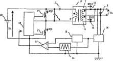
图5是一个传统DC-DC转换器的方框电路图。 Fig. 5 is a block circuit diagram of a conventional DC-DC converter. the
现参考图5,传统的DC-DC转换器包括:第一串联电路,其包括金属氧化物半导体场效应晶体管(MOSFET)1和2且并联到直流电源10;第二串联电路,其包括电容3和变压器9的初级绕组,且并联到MOSFET 2;一缓冲电容4并联到MOSFET 2上;以及包括二极管11的整流及平滑电路5连接到变压器9的次级绕组7,而二极管12连接到变压器9的另一次级绕组8。第一输出电压检测电路16检测输出电压V0。三角波发生器电路14产生三角波信号,其频率相应于输出电压V0与参考输出电压之差而变化。比较器15比较该三角波信号的频率和通断比设定电路(on-off ratio setting circuit)13的输出。驱动器电路18按固定的50%的通断比交替地接通和断开MOSFET 1和2。 Referring now to FIG. 5, a conventional DC-DC converter includes: a first series circuit comprising metal oxide semiconductor field effect transistors (MOSFETs) 1 and 2 connected in parallel to a
如上所述,图5所示的传统DC-DC转换器通过以固定的通断比改变MOSFET 1和2的开关频率Fs而控制输出电压。因为上述的DC-DC转换器是通常的电流共振型转换器,且因为其操作与普通的一样,所以省略对传统DC-DC转换器的详细说明。 As mentioned above, the conventional DC-DC converter shown in Figure 5 controls the output voltage by varying the switching frequency Fs of
在传统DC-DC转换器中,变压器的激励电感应足够低以防止开关频率增加太大。 In conventional DC-DC converters, the excitation inductance of the transformer should be low enough to prevent the switching frequency from increasing too much. the
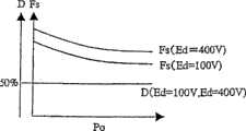
图6是关于开关频率Fs在DC电源电压Ed为100V和400V下,通断比D对输出功率Po的一组曲线。在传统的DC-DC变压器中,虽然开关频率根据负载条件和来自DC电源的输入电压而在一定程度上变化,但通断比D几乎没有显示出变化。 Fig. 6 is a set of curves of on-off ratio D versus output power Po about switching frequency Fs under DC power supply voltage Ed of 100V and 400V. In conventional DC-DC transformers, although the switching frequency varies to some extent depending on the load conditions and the input voltage from the DC power supply, the on-off ratio D shows little variation. the
图7是一波形图,描述分别流经MOSFET1和2的电流IQ1和IQ2,以及分别流经二极管11和12的电流ID11和ID12,其中二极管11和 12连接到额定负载条件下的变压器次级绕组一侧。图8是一波形图,描述分别流经MOSFET1和2的电流IQ1和IQ2,以及分别流经二极管11和12的电流ID11和ID12,其中二极管11和12连接到轻负载条件下的变压器次级绕组一侧。 Figure 7 is a waveform diagram depicting the currents IQ1 and IQ2 flowing through
减少变压器的激励电感从而防止在轻负载条件下开关频率增加太大,结果使得在额定负载和轻负载条件下高激励电流流入变压器,如图7和图8所示的IQ1和IQ2。该激励电流引起电抗性电流,其进一步引起在电路中阻抗上的损失,该阻抗例如为MOSFET和变压器绕组的电阻。由于所引起的损失,上述DC-DC转换器的转换效率低于轻负载条件下的转换效率。 Reducing the excitation inductance of the transformer prevents the switching frequency from increasing too much under light load conditions, resulting in high excitation currents flowing into the transformer at both rated and light load conditions, as shown in Figure 7 and Figure 8 for IQ1 and IQ2. This excitation current induces a reactive current, which further causes losses in the circuit in impedance, such as the resistance of MOSFETs and transformer windings. Due to the losses incurred, the conversion efficiency of the above-mentioned DC-DC converter is lower than that under light load conditions. the
按前述观点,本发明的一个目标是提供一种控制DC-DC转换器的方法,其有利于防止开关频率在轻负载条件下增加,且促进DC-DC转换器的转换效率。 In view of the foregoing, an object of the present invention is to provide a method of controlling a DC-DC converter which is advantageous in preventing the switching frequency from increasing under light load conditions and promoting the conversion efficiency of the DC-DC converter. the
发明内容Contents of the invention
根据本发明,提供了一种控制DC-DC转换器的方法,该DC-DC转换器包括:第一串联电路,其包括两个开关器件且连接到DC电压的正端和负端之间;和第二串联电路,其包括一个或多个电容和变压器的初级绕组且并联地连接到一个开关器件上,该DC-DC转换器接通或断开开关器件以于变压器的次级绕组的两端产生正的和负的电压。该DC-DC转换器导通产生于变压器的次级绕组两端的正和负的电压的半波整流或全波整流以得到一DC输出,所述方法包括:所述两个开关器件的通断比相应于输出电压而改变,所述开关频率相应于DC电源电压而改变,并且,对于所述通断比,以额定负载时为50%附近、或负载小时小于50%的方式分别进行控制,对于所述开关频率,以输入电压高时则高、或输入电压低时则低的方式分别进行控制。 According to the present invention, there is provided a method of controlling a DC-DC converter comprising: a first series circuit comprising two switching devices and connected between a positive terminal and a negative terminal of a DC voltage; and a second series circuit comprising one or more capacitors and the primary winding of the transformer and connected in parallel to a switching device, the DC-DC converter turns on or off the switching device for both of the secondary windings of the transformer produces positive and negative voltages. The DC-DC converter conducts half-wave rectification or full-wave rectification of the positive and negative voltages generated across the secondary winding of the transformer to obtain a DC output, the method comprising: an on-off ratio of the two switching devices The switching frequency is changed corresponding to the output voltage, and the switching frequency is changed corresponding to the DC power supply voltage, and the on-off ratio is controlled so that it is around 50% at the rated load or less than 50% when the load is small. The switching frequency is individually controlled so as to increase when the input voltage is high or to decrease when the input voltage is low. the
本发明还提供了一种控制DC-DC转换器的方法,该DC-DC转换器包括:第一串联电路,其包括两个开关器件且连接到DC电压的正端和负端之间;和第二串联电路,其包括一个或多个电容和变压器的初级绕组且并联地连接到一个开关器件上,该DC-DC转换器接通或断开开关器件以于变压器的次级绕组的两端产生正的和负的电压。该 DC-DC转换器导通产生于变压器的次级绕组两端的正和负的电压的半波整流或全波整流以得到一DC输出,所述方法包括:在使所述两个开关器件的通断比为固定的状态下,进行改变所述开关频率的控制,而当所述开关频率达到一预定值后,在使所述开关频率为固定的状态下改变所述通断比,从而防止所述开关频率为所述预定值以上。 The present invention also provides a method of controlling a DC-DC converter comprising: a first series circuit comprising two switching devices connected between a positive terminal and a negative terminal of a DC voltage; and The second series circuit, which includes one or more capacitors and the primary winding of the transformer and is connected in parallel to a switching device, the DC-DC converter turns on or off the switching device to connect the two ends of the secondary winding of the transformer Generate positive and negative voltages. The DC-DC converter conducts half-wave rectification or full-wave rectification of positive and negative voltages generated at both ends of the secondary winding of the transformer to obtain a DC output, the method comprising: passing the two switching devices When the off-ratio is fixed, the control of changing the switching frequency is performed, and when the switching frequency reaches a predetermined value, the on-off ratio is changed while the switching frequency is fixed, thereby preventing the The switching frequency is above the predetermined value. the
附图说明Description of drawings
图1是一DC-DC转换器的方框电路图,该DC-DC转换器通过根据本发明的第一实施方案的控制方法来控制。 Fig. 1 is a block circuit diagram of a DC-DC converter controlled by a control method according to a first embodiment of the present invention. the
图2是电源电压Ed为100V和400V时,一组关于开关频率Fs和通断比D与输出功率Po的曲线。 Figure 2 is a set of curves about switching frequency Fs, on-off ratio D and output power Po when the power supply voltage Ed is 100V and 400V. the
图3是一DC-DC转换器的方框电路图,该DC-DC转换器通过根据本发明的第二实施方案的控制方法来控制。 Fig. 3 is a block circuit diagram of a DC-DC converter controlled by a control method according to a second embodiment of the present invention. the
图4是电源电压Ed为400V时,一对关于开关频率Fs和通断比D与输出功率Po的曲线。 Figure 4 is a pair of curves about switching frequency Fs, on-off ratio D and output power Po when the power supply voltage Ed is 400V. the
图5是一传统DC-DC转换器的方框电路图。 Fig. 5 is a block circuit diagram of a conventional DC-DC converter. the
图6是DC电源电压Ed为100V和400V时,一组关于开关频率Fs和通断比D与输出功率Po的曲线。 Figure 6 is a set of curves about switching frequency Fs, on-off ratio D and output power Po when the DC power supply voltage Ed is 100V and 400V. the
图7是一波形图,说明在额定负载条件下,流过图5中MOSFET的电流,以及流过连接到图5中变压器的次级侧的二极管的电流。 FIG. 7 is a waveform diagram illustrating the current flowing through the MOSFET in FIG. 5 and the current flowing through the diode connected to the secondary side of the transformer in FIG. 5 under rated load conditions. the
图8是一波形图,说明在轻负载条件下,流过图5中MOSFET的电流,以及流过连接到图5中变压器的次级侧的二极管的电流。 FIG. 8 is a waveform diagram illustrating the current flowing through the MOSFET in FIG. 5 and the current flowing through the diode connected to the secondary side of the transformer in FIG. 5 under light load conditions. the
具体实施方式Detailed ways
现在将参考说明本发明优选实施方案的附图而详细说明本发明。所有附图中,如图5到图8中所用的相同的参考编号和符号代表相同的构成元件,为了简洁起见,略去重复的说明。 The present invention will now be described in detail with reference to the accompanying drawings illustrating preferred embodiments of the invention. In all the drawings, the same reference numerals and symbols used in FIGS. 5 to 8 denote the same constituent elements, and repeated descriptions are omitted for the sake of brevity. the
图1是一DC-DC转换器的方框图,该DC-DC转换器通过根据本发明的第一实施方案的控制方法来控制。 Fig. 1 is a block diagram of a DC-DC converter controlled by a control method according to a first embodiment of the present invention. the
参考图1,根据第一实施方案的DC-DC转换器的主电路和传统的DC-DC转换器的主电路相同。根据本发明第一实施方案的DC-DC转换器和传统的DC-DC转换器不同,这是因为根据第一实施方案的DC-DC转换器进一步包括了第二电压检测器电路17,其输出被输入到三角波发生电路14,也因为第一电压检测电路16的输出还被输入到通断比设定电路13。 Referring to FIG. 1, the main circuit of the DC-DC converter according to the first embodiment is the same as that of a conventional DC-DC converter. The DC-DC converter according to the first embodiment of the present invention is different from conventional DC-DC converters because the DC-DC converter according to the first embodiment further includes a second
图2是DC电源电压Ed为100V和400V时,关于开关频率Fs和通断比D与输出功率Po(电压Vo与电流ID11和ID12的乘积)的一组曲线。 Fig. 2 is a set of curves about switching frequency Fs, on-off ratio D and output power Po (product of voltage Vo and current ID11 and ID12) when DC power supply voltage Ed is 100V and 400V. the
在上述电路中,由三角波发生电路14产生的三角波信号的振荡频率,也就是开关频率Fs,相应于由DC电源馈入的输入电压Ed而改变,且被第二电压检测器电路17检测。使得对应于100V和400V的输入电压Ed的三角波信号的振荡频率互不相同。在同一时间,MOSFET1和2的通断比D相应于被第一电压检测器电路16检测到的输出电压Vo而调整(改变),如图2所示。由此控制输出电压Vo。对任意一个DC电源电压Ed,开关频率Fs被预先设定为一个值,在该值下,通断比D在额定负载条件下大约是50%,因为在本发明所应用的DC-DC转换器中,最高转换效率是在通断比大约为50%时获得的。 In the above circuit, the oscillation frequency of the triangular wave signal generated by the triangular
图3是一个DC-DC转换器的方框电路图,该DC-DC转换器通过根据本发明的第二个实施方案的控制方法来控制。 Fig. 3 is a block circuit diagram of a DC-DC converter controlled by a control method according to a second embodiment of the present invention. the
现参考图3,根据第二实施方案的DC-DC转换器的主电路和传统DC-DC转换器的主电路相同。根据该第二实施方案的DC-DC转换器则不同于传统的DC-DC转换器,这是因为其中来自第一电压检测器电路16的输出不仅被输入到三角波发生器电路14,还被输入到通断比设定电路13。 Referring now to FIG. 3, the main circuit of the DC-DC converter according to the second embodiment is the same as that of the conventional DC-DC converter. The DC-DC converter according to this second embodiment is different from the conventional DC-DC converter because the output from the first
图4是DC电源电压Ed为400V时,关于开关频率Fs和通断比D与输出功率Po的一对曲线。 Figure 4 is a pair of curves about switching frequency Fs, on-off ratio D and output power Po when the DC power supply voltage Ed is 400V. the
如图3所示配置的电路基本通过改变开关频率Fs同时将通断比D固定于50%来调整输出电压Vo。在轻负载和类似条件下,当开关频率Fs超过一特定限制时,图3中的DC-DC转换器通过改变通断比D同时将开关频率Fs固定于如图4中所示的一个特定值来控制输出电压 Vo。 The circuit configured as shown in FIG. 3 basically adjusts the output voltage Vo by changing the switching frequency Fs while fixing the on-off ratio D at 50%. Under light load and similar conditions, when the switching frequency Fs exceeds a certain limit, the DC-DC converter in Figure 3 fixes the switching frequency Fs at a certain value as shown in Figure 4 by changing the on-off ratio D to control the output voltage Vo. the
发明效果Invention effect
因为根据本发明而防止了开关频率显著增加,且减小了变压器的激励电流,甚至当变压器的激励电感比传统的激励电感高时,电抗性电流所引起的损失也被减小。根据本发明,DC-DC转换器的转换效率特别是在轻负载条件下得到了改进。 Since the switching frequency is prevented from significantly increasing according to the present invention and the exciting current of the transformer is reduced, even when the exciting inductance of the transformer is higher than conventional exciting inductance, the loss caused by the reactive current is also reduced. According to the present invention, the conversion efficiency of the DC-DC converter is improved especially under light load conditions. the
参考数字和符号的指代物Designators of reference numerals and symbols
1,2:金属氧化物半导体场效应晶体管(MOSFET) 1, 2: Metal Oxide Semiconductor Field Effect Transistor (MOSFET)
3,4,5:电容 3, 4, 5: capacitance
6,7,8:绕组 6, 7, 8: winding
9:变压器 9: Transformer
10:DC电压源 10: DC voltage source
11,12:二极管 11, 12: Diodes
13:通断比设定电路 13: On-off ratio setting circuit
14:三角波发生电路 14: Triangular wave generating circuit
15:比较器 15: Comparator
16:第一电压检测器电路 16: The first voltage detector circuit
17:第二电压检测器电路 17: Second voltage detector circuit
18:驱动器电路 18: Driver circuit
Claims (1)
Translated fromChineseApplications Claiming Priority (3)
| Application Number | Priority Date | Filing Date | Title |
|---|---|---|---|
| JP2002-218285 | 2002-07-26 | ||
| JP2002218285AJP4217950B2 (en) | 2002-07-26 | 2002-07-26 | Control method of DC / DC converter |
| JP2002218285 | 2002-07-26 |
Related Parent Applications (1)
| Application Number | Title | Priority Date | Filing Date |
|---|---|---|---|
| CNB031502741ADivisionCN100413194C (en) | 2002-07-26 | 2003-07-23 | A method of controlling a DC-DC converter |
Publications (2)
| Publication Number | Publication Date |
|---|---|
| CN101242144A CN101242144A (en) | 2008-08-13 |
| CN101242144Btrue CN101242144B (en) | 2012-03-28 |
Family
ID=31884294
Family Applications (2)
| Application Number | Title | Priority Date | Filing Date |
|---|---|---|---|
| CN2008100866348AExpired - Fee RelatedCN101242144B (en) | 2002-07-26 | 2003-07-23 | A method of controlling a DC-DC converter |
| CNB031502741AExpired - Fee RelatedCN100413194C (en) | 2002-07-26 | 2003-07-23 | A method of controlling a DC-DC converter |
Family Applications After (1)
| Application Number | Title | Priority Date | Filing Date |
|---|---|---|---|
| CNB031502741AExpired - Fee RelatedCN100413194C (en) | 2002-07-26 | 2003-07-23 | A method of controlling a DC-DC converter |
Country Status (3)
| Country | Link |
|---|---|
| US (1) | US6900996B2 (en) |
| JP (1) | JP4217950B2 (en) |
| CN (2) | CN101242144B (en) |
Families Citing this family (13)
| Publication number | Priority date | Publication date | Assignee | Title |
|---|---|---|---|---|
| JP4626338B2 (en)* | 2005-02-25 | 2011-02-09 | サンケン電気株式会社 | DC converter |
| CN1925290B (en)* | 2005-09-02 | 2012-06-06 | 中兴通讯股份有限公司 | Positive-negative voltage conversion circuit |
| JP5691137B2 (en)* | 2008-05-14 | 2015-04-01 | 富士電機株式会社 | Switching power supply |
| JP5419286B2 (en)* | 2010-03-26 | 2014-02-19 | ニチコン株式会社 | Forward converter |
| CN103329420B (en)* | 2011-01-26 | 2015-12-02 | 株式会社村田制作所 | switching power supply circuit |
| KR101964224B1 (en) | 2012-02-03 | 2019-04-01 | 후지 덴키 가부시키가이샤 | Control device for resonance-type dc-dc converter |
| JP5995139B2 (en)* | 2012-10-12 | 2016-09-21 | 富士電機株式会社 | Bidirectional DC / DC converter |
| CN103728528B (en)* | 2013-12-05 | 2016-09-21 | 国家电网公司 | A kind of MMC submodule diagnostic method based on switching frequency statistics |
| US9729072B2 (en) | 2014-02-11 | 2017-08-08 | Fairchild Korea Semiconductor Ltd. | Resonant converter and driving method thereof |
| KR20150095180A (en) | 2014-02-11 | 2015-08-20 | 페어차일드코리아반도체 주식회사 | Switch control circuit and resonant converter comprising thereof |
| US9627988B2 (en)* | 2014-02-11 | 2017-04-18 | Fairchild Korea Semiconductor Ltd. | Switch control circuit and resonant converter including the same |
| US9647528B2 (en) | 2014-02-11 | 2017-05-09 | Fairchild Korea Semiconductor Ltd | Switch control circuit and resonant converter including the same |
| WO2016149319A1 (en)* | 2015-03-16 | 2016-09-22 | Finsix Corporation | Control of resonant power converters |
Citations (2)
| Publication number | Priority date | Publication date | Assignee | Title |
|---|---|---|---|---|
| CN1298223A (en)* | 1999-10-29 | 2001-06-06 | 索尼公司 | Secondary lateral parallel and series resonance power circuit for switch |
| US20020080634A1 (en)* | 2000-11-10 | 2002-06-27 | Fuji Electric Co., Ltd. | DC/DC Converter and control method thereof |
Family Cites Families (7)
| Publication number | Priority date | Publication date | Assignee | Title |
|---|---|---|---|---|
| JPH07118918B2 (en)* | 1989-01-26 | 1995-12-18 | 三菱電機株式会社 | DC / DC power supply |
| JPH04180U (en)* | 1990-04-11 | 1992-01-06 | ||
| JPH0731143A (en)* | 1993-07-09 | 1995-01-31 | Murata Mfg Co Ltd | Voltage resonance converter |
| JPH07123706A (en) | 1993-10-25 | 1995-05-12 | Canon Inc | Dc-dc converter |
| JP3511195B2 (en)* | 1997-09-03 | 2004-03-29 | 株式会社ルネサステクノロジ | Voltage conversion circuit |
| JP2000116027A (en)* | 1998-03-10 | 2000-04-21 | Fiderikkusu:Kk | Power supply device |
| KR100426606B1 (en)* | 2000-10-30 | 2004-04-08 | 가부시키가이샤 무라타 세이사쿠쇼 | DC―DC Convertor and an electronic device using the same |
- 2002
- 2002-07-26JPJP2002218285Apatent/JP4217950B2/ennot_activeExpired - Fee Related
- 2003
- 2003-07-23CNCN2008100866348Apatent/CN101242144B/ennot_activeExpired - Fee Related
- 2003-07-23CNCNB031502741Apatent/CN100413194C/ennot_activeExpired - Fee Related
- 2003-07-28USUS10/628,586patent/US6900996B2/ennot_activeExpired - Lifetime
Patent Citations (2)
| Publication number | Priority date | Publication date | Assignee | Title |
|---|---|---|---|---|
| CN1298223A (en)* | 1999-10-29 | 2001-06-06 | 索尼公司 | Secondary lateral parallel and series resonance power circuit for switch |
| US20020080634A1 (en)* | 2000-11-10 | 2002-06-27 | Fuji Electric Co., Ltd. | DC/DC Converter and control method thereof |
Non-Patent Citations (2)
| Title |
|---|
| JP平11-89222A 1999.03.30 |
| JP平7-31143A 1995.01.31 |
Also Published As
| Publication number | Publication date |
|---|---|
| US20040105280A1 (en) | 2004-06-03 |
| JP4217950B2 (en) | 2009-02-04 |
| US6900996B2 (en) | 2005-05-31 |
| CN1477774A (en) | 2004-02-25 |
| CN100413194C (en) | 2008-08-20 |
| JP2004064859A (en) | 2004-02-26 |
| CN101242144A (en) | 2008-08-13 |
Similar Documents
| Publication | Publication Date | Title |
|---|---|---|
| US7301785B2 (en) | Switching power supply circuit | |
| US6654259B2 (en) | Resonance type switching power supply unit | |
| US6366476B1 (en) | Switching power supply apparatus with active clamp circuit | |
| US6396717B2 (en) | Switching power supply having an improved power factor by voltage feedback | |
| CN101288219B (en) | Load resonant power supply for ozone generator | |
| EP1150418B1 (en) | Switching power supply apparatus with active voltage clamp circuit | |
| US7388760B2 (en) | Switching power supply circuit | |
| JPH09215337A (en) | Voltage conversion circuit apparatus for supplying energy to a high output electric load | |
| JPH02184267A (en) | Series resonance inverter with non-loss snabber-reset part | |
| CN101242144B (en) | A method of controlling a DC-DC converter | |
| KR20020029904A (en) | Switching power supply circuit | |
| US7821801B2 (en) | Power factor correction method for AC/DC converters and corresponding converter | |
| US5864472A (en) | Apparatus for controlling a multiresonant self-oscillating converter circuit | |
| JP4359026B2 (en) | Electric circuit device for generating low power rectification low voltage from AC voltage | |
| US7158389B2 (en) | Switching power supply circuit | |
| JP2000058252A (en) | High frequency heating equipment | |
| JP4683364B2 (en) | Composite resonant switching power supply | |
| KR100439414B1 (en) | DC/DC converter of Insulation type and Uninterruptible power supply used the same apparatus | |
| JP2002262568A (en) | Switching power circuit | |
| JP3163655B2 (en) | Inverter device | |
| JP2002281756A (en) | Switching converter circuit | |
| JP3230560B2 (en) | DC power supply | |
| JPH0622546A (en) | Switching regulator | |
| JP2001086747A (en) | Power-supply unit | |
| JPH0745361A (en) | High frequency heating device |
Legal Events
| Date | Code | Title | Description |
|---|---|---|---|
| C06 | Publication | ||
| PB01 | Publication | ||
| C10 | Entry into substantive examination | ||
| SE01 | Entry into force of request for substantive examination | ||
| ASS | Succession or assignment of patent right | Owner name:FUJI MOTOR SYSTEM CO., LTD. Free format text:FORMER OWNER: FUJI MOTOR ELECTRONICS TECHNOLOGY CO., LTD. Effective date:20100510 Owner name:FUJI MOTOR ELECTRONICS TECHNOLOGY CO., LTD. Free format text:FORMER OWNER: FUJI MOTOR STOCK CO., LTD. Effective date:20100510 | |
| C41 | Transfer of patent application or patent right or utility model | ||
| COR | Change of bibliographic data | Free format text:CORRECT: ADDRESS; FROM: KAWASAKI CITY, JAPAN TO: TOKYO, JAPAN | |
| TA01 | Transfer of patent application right | Effective date of registration:20100510 Address after:Tokyo, Japan Applicant after:Fuji Electric Systems Co.,Ltd. Address before:Tokyo, Japan Applicant before:Fuji Electric Device Technology Co.,Ltd. Effective date of registration:20100510 Address after:Tokyo, Japan Applicant after:Fuji Electric Device Technology Co.,Ltd. Address before:Kawasaki, Japan Applicant before:Fuji Electric Holdings Co.,Ltd. | |
| ASS | Succession or assignment of patent right | Owner name:FUJI ELECTRIC CO., LTD. Free format text:FORMER OWNER: FUJI ELECTRIC SYSTEMS CO., LTD. Effective date:20111009 | |
| C41 | Transfer of patent application or patent right or utility model | ||
| TA01 | Transfer of patent application right | Effective date of registration:20111009 Address after:Japan's Kawasaki City Applicant after:FUJI ELECTRIC Co.,Ltd. Address before:Tokyo, Japan Applicant before:Fuji Electric Systems Co.,Ltd. | |
| C14 | Grant of patent or utility model | ||
| GR01 | Patent grant | ||
| CF01 | Termination of patent right due to non-payment of annual fee | Granted publication date:20120328 | |
| CF01 | Termination of patent right due to non-payment of annual fee |