CN101231437A - Liquid crystal display device and method of manufacturing the same - Google Patents
Liquid crystal display device and method of manufacturing the sameDownload PDFInfo
- Publication number
- CN101231437A CN101231437ACNA2008100039468ACN200810003946ACN101231437ACN 101231437 ACN101231437 ACN 101231437ACN A2008100039468 ACNA2008100039468 ACN A2008100039468ACN 200810003946 ACN200810003946 ACN 200810003946ACN 101231437 ACN101231437 ACN 101231437A
- Authority
- CN
- China
- Prior art keywords
- electrode
- liquid crystal
- display device
- crystal display
- insulating film
- Prior art date
- Legal status (The legal status is an assumption and is not a legal conclusion. Google has not performed a legal analysis and makes no representation as to the accuracy of the status listed.)
- Granted
Links
Images


Classifications
- G—PHYSICS
- G02—OPTICS
- G02F—OPTICAL DEVICES OR ARRANGEMENTS FOR THE CONTROL OF LIGHT BY MODIFICATION OF THE OPTICAL PROPERTIES OF THE MEDIA OF THE ELEMENTS INVOLVED THEREIN; NON-LINEAR OPTICS; FREQUENCY-CHANGING OF LIGHT; OPTICAL LOGIC ELEMENTS; OPTICAL ANALOGUE/DIGITAL CONVERTERS
- G02F1/00—Devices or arrangements for the control of the intensity, colour, phase, polarisation or direction of light arriving from an independent light source, e.g. switching, gating or modulating; Non-linear optics
- G02F1/01—Devices or arrangements for the control of the intensity, colour, phase, polarisation or direction of light arriving from an independent light source, e.g. switching, gating or modulating; Non-linear optics for the control of the intensity, phase, polarisation or colour
- G02F1/13—Devices or arrangements for the control of the intensity, colour, phase, polarisation or direction of light arriving from an independent light source, e.g. switching, gating or modulating; Non-linear optics for the control of the intensity, phase, polarisation or colour based on liquid crystals, e.g. single liquid crystal display cells
- G02F1/133—Constructional arrangements; Operation of liquid crystal cells; Circuit arrangements
- G02F1/1333—Constructional arrangements; Manufacturing methods
- G02F1/1343—Electrodes
- G02F1/134309—Electrodes characterised by their geometrical arrangement
- G—PHYSICS
- G02—OPTICS
- G02F—OPTICAL DEVICES OR ARRANGEMENTS FOR THE CONTROL OF LIGHT BY MODIFICATION OF THE OPTICAL PROPERTIES OF THE MEDIA OF THE ELEMENTS INVOLVED THEREIN; NON-LINEAR OPTICS; FREQUENCY-CHANGING OF LIGHT; OPTICAL LOGIC ELEMENTS; OPTICAL ANALOGUE/DIGITAL CONVERTERS
- G02F1/00—Devices or arrangements for the control of the intensity, colour, phase, polarisation or direction of light arriving from an independent light source, e.g. switching, gating or modulating; Non-linear optics
- G02F1/01—Devices or arrangements for the control of the intensity, colour, phase, polarisation or direction of light arriving from an independent light source, e.g. switching, gating or modulating; Non-linear optics for the control of the intensity, phase, polarisation or colour
- G02F1/13—Devices or arrangements for the control of the intensity, colour, phase, polarisation or direction of light arriving from an independent light source, e.g. switching, gating or modulating; Non-linear optics for the control of the intensity, phase, polarisation or colour based on liquid crystals, e.g. single liquid crystal display cells
- G02F1/133—Constructional arrangements; Operation of liquid crystal cells; Circuit arrangements
- G02F1/136—Liquid crystal cells structurally associated with a semi-conducting layer or substrate, e.g. cells forming part of an integrated circuit
- G—PHYSICS
- G02—OPTICS
- G02F—OPTICAL DEVICES OR ARRANGEMENTS FOR THE CONTROL OF LIGHT BY MODIFICATION OF THE OPTICAL PROPERTIES OF THE MEDIA OF THE ELEMENTS INVOLVED THEREIN; NON-LINEAR OPTICS; FREQUENCY-CHANGING OF LIGHT; OPTICAL LOGIC ELEMENTS; OPTICAL ANALOGUE/DIGITAL CONVERTERS
- G02F1/00—Devices or arrangements for the control of the intensity, colour, phase, polarisation or direction of light arriving from an independent light source, e.g. switching, gating or modulating; Non-linear optics
- G02F1/01—Devices or arrangements for the control of the intensity, colour, phase, polarisation or direction of light arriving from an independent light source, e.g. switching, gating or modulating; Non-linear optics for the control of the intensity, phase, polarisation or colour
- G02F1/13—Devices or arrangements for the control of the intensity, colour, phase, polarisation or direction of light arriving from an independent light source, e.g. switching, gating or modulating; Non-linear optics for the control of the intensity, phase, polarisation or colour based on liquid crystals, e.g. single liquid crystal display cells
- G02F1/133—Constructional arrangements; Operation of liquid crystal cells; Circuit arrangements
- G02F1/1333—Constructional arrangements; Manufacturing methods
- G02F1/133357—Planarisation layers
- G—PHYSICS
- G02—OPTICS
- G02F—OPTICAL DEVICES OR ARRANGEMENTS FOR THE CONTROL OF LIGHT BY MODIFICATION OF THE OPTICAL PROPERTIES OF THE MEDIA OF THE ELEMENTS INVOLVED THEREIN; NON-LINEAR OPTICS; FREQUENCY-CHANGING OF LIGHT; OPTICAL LOGIC ELEMENTS; OPTICAL ANALOGUE/DIGITAL CONVERTERS
- G02F1/00—Devices or arrangements for the control of the intensity, colour, phase, polarisation or direction of light arriving from an independent light source, e.g. switching, gating or modulating; Non-linear optics
- G02F1/01—Devices or arrangements for the control of the intensity, colour, phase, polarisation or direction of light arriving from an independent light source, e.g. switching, gating or modulating; Non-linear optics for the control of the intensity, phase, polarisation or colour
- G02F1/13—Devices or arrangements for the control of the intensity, colour, phase, polarisation or direction of light arriving from an independent light source, e.g. switching, gating or modulating; Non-linear optics for the control of the intensity, phase, polarisation or colour based on liquid crystals, e.g. single liquid crystal display cells
- G02F1/133—Constructional arrangements; Operation of liquid crystal cells; Circuit arrangements
- G02F1/1333—Constructional arrangements; Manufacturing methods
- G02F1/1343—Electrodes
- G02F1/134309—Electrodes characterised by their geometrical arrangement
- G02F1/134372—Electrodes characterised by their geometrical arrangement for fringe field switching [FFS] where the common electrode is not patterned
- G—PHYSICS
- G02—OPTICS
- G02F—OPTICAL DEVICES OR ARRANGEMENTS FOR THE CONTROL OF LIGHT BY MODIFICATION OF THE OPTICAL PROPERTIES OF THE MEDIA OF THE ELEMENTS INVOLVED THEREIN; NON-LINEAR OPTICS; FREQUENCY-CHANGING OF LIGHT; OPTICAL LOGIC ELEMENTS; OPTICAL ANALOGUE/DIGITAL CONVERTERS
- G02F1/00—Devices or arrangements for the control of the intensity, colour, phase, polarisation or direction of light arriving from an independent light source, e.g. switching, gating or modulating; Non-linear optics
- G02F1/01—Devices or arrangements for the control of the intensity, colour, phase, polarisation or direction of light arriving from an independent light source, e.g. switching, gating or modulating; Non-linear optics for the control of the intensity, phase, polarisation or colour
- G02F1/13—Devices or arrangements for the control of the intensity, colour, phase, polarisation or direction of light arriving from an independent light source, e.g. switching, gating or modulating; Non-linear optics for the control of the intensity, phase, polarisation or colour based on liquid crystals, e.g. single liquid crystal display cells
- G02F1/133—Constructional arrangements; Operation of liquid crystal cells; Circuit arrangements
- G02F1/1333—Constructional arrangements; Manufacturing methods
- G02F1/1343—Electrodes
- G02F1/134309—Electrodes characterised by their geometrical arrangement
- G02F1/134381—Hybrid switching mode, i.e. for applying an electric field with components parallel and orthogonal to the substrates
- G—PHYSICS
- G02—OPTICS
- G02F—OPTICAL DEVICES OR ARRANGEMENTS FOR THE CONTROL OF LIGHT BY MODIFICATION OF THE OPTICAL PROPERTIES OF THE MEDIA OF THE ELEMENTS INVOLVED THEREIN; NON-LINEAR OPTICS; FREQUENCY-CHANGING OF LIGHT; OPTICAL LOGIC ELEMENTS; OPTICAL ANALOGUE/DIGITAL CONVERTERS
- G02F1/00—Devices or arrangements for the control of the intensity, colour, phase, polarisation or direction of light arriving from an independent light source, e.g. switching, gating or modulating; Non-linear optics
- G02F1/01—Devices or arrangements for the control of the intensity, colour, phase, polarisation or direction of light arriving from an independent light source, e.g. switching, gating or modulating; Non-linear optics for the control of the intensity, phase, polarisation or colour
- G02F1/13—Devices or arrangements for the control of the intensity, colour, phase, polarisation or direction of light arriving from an independent light source, e.g. switching, gating or modulating; Non-linear optics for the control of the intensity, phase, polarisation or colour based on liquid crystals, e.g. single liquid crystal display cells
- G02F1/133—Constructional arrangements; Operation of liquid crystal cells; Circuit arrangements
- G02F1/136—Liquid crystal cells structurally associated with a semi-conducting layer or substrate, e.g. cells forming part of an integrated circuit
- G02F1/1362—Active matrix addressed cells
- G02F1/136227—Through-hole connection of the pixel electrode to the active element through an insulation layer
- G—PHYSICS
- G02—OPTICS
- G02F—OPTICAL DEVICES OR ARRANGEMENTS FOR THE CONTROL OF LIGHT BY MODIFICATION OF THE OPTICAL PROPERTIES OF THE MEDIA OF THE ELEMENTS INVOLVED THEREIN; NON-LINEAR OPTICS; FREQUENCY-CHANGING OF LIGHT; OPTICAL LOGIC ELEMENTS; OPTICAL ANALOGUE/DIGITAL CONVERTERS
- G02F2201/00—Constructional arrangements not provided for in groups G02F1/00 - G02F7/00
- G02F2201/40—Arrangements for improving the aperture ratio
Landscapes
- Physics & Mathematics (AREA)
- Nonlinear Science (AREA)
- Mathematical Physics (AREA)
- Chemical & Material Sciences (AREA)
- Crystallography & Structural Chemistry (AREA)
- General Physics & Mathematics (AREA)
- Optics & Photonics (AREA)
- Geometry (AREA)
- Liquid Crystal (AREA)
- Engineering & Computer Science (AREA)
- Microelectronics & Electronic Packaging (AREA)
Abstract
Translated fromChinese
Description
Translated fromChinese技术领域technical field
本发明涉及一种FFS模式的液晶显示装置及其制造方法,不用增加制造工时就能够制造,在平坦化膜上配置有像素电极及共用电极,并且可以实现高开口率及高显示画质。The invention relates to an FFS mode liquid crystal display device and a manufacturing method thereof, which can be manufactured without increasing manufacturing man-hours, and a pixel electrode and a common electrode are arranged on a planarization film, and can realize high aperture ratio and high display quality.
背景技术Background technique
液晶显示装置已被广泛使用的是纵向电场方式的液晶显示装置,具有:一对透明基板,在表面上形成电极等;和液晶层,夹持于该一对基板间;通过对两个基板上的电极施加电压使液晶重新排列来显示各种信息。这种纵向电场方式的液晶显示装置一般是TN(Twisted Nematic,扭曲向列)模式,但是因为存在视场角狭窄这样的问题所在,所以正在开发VA(Vertical Alignment,垂直取向)模式和MVA(Multidomain VerticalAlignment,多畴垂直取向)模式等各种改进后的纵向电场方式的液晶显示装置。The liquid crystal display device that has been widely used is the liquid crystal display device of the longitudinal electric field method, which has: a pair of transparent substrates on which electrodes and the like are formed on the surface; and a liquid crystal layer sandwiched between the pair of substrates; The electrodes apply a voltage to rearrange the liquid crystals to display various information. This type of longitudinal electric field liquid crystal display device is generally TN (Twisted Nematic, twisted nematic) mode, but because of the problem of narrow viewing angle, VA (Vertical Alignment, vertical alignment) mode and MVA (Multidomain alignment) mode are being developed. Vertical Alignment, multi-domain vertical alignment) mode and other improved liquid crystal display devices in the vertical electric field mode.
另一方面,和上述纵向电场方式的液晶显示装置不同,只在一方基板上具备由像素电极及共用电极构成的一对电极的IPS(In-Plane Switching,面内开关)模式或FFS(Fringe Field Switching,边缘场开关)模式的液晶显示装置,也已众所周知。On the other hand, unlike the liquid crystal display device of the above-mentioned vertical electric field method, the IPS (In-Plane Switching, in-plane switch) mode or the FFS (Fringe Field Switching (fringe field switching) mode liquid crystal display devices are also well known.
其中,IPS模式的液晶显示装置将一对电极配置于同一层,使给液晶施加的电场方向为与基板大致平行的方向,使液晶分子按平行于基板的方向重新排列。因此,该IPS模式的液晶显示装置也称为横向电场方式的液晶显示装置,和上述纵向电场方式的液晶显示装置相比,具有视场角非常宽这样的优点。但是,IPS模式的液晶显示装置因为为了给液晶施加电场,将一对电极设置在同一层,所以位于像素电极上侧的液晶分子没有被充分驱动,存在导致透射率等下降之类的问题所在。Among them, in the IPS mode liquid crystal display device, a pair of electrodes are arranged on the same layer, so that the direction of the electric field applied to the liquid crystal is roughly parallel to the substrate, so that the liquid crystal molecules are rearranged in a direction parallel to the substrate. Therefore, this IPS mode liquid crystal display device is also called a transverse electric field type liquid crystal display device, and has an advantage of a very wide viewing angle compared with the above-mentioned vertical electric field type liquid crystal display device. However, in an IPS mode liquid crystal display device, since a pair of electrodes are provided on the same layer in order to apply an electric field to the liquid crystal, the liquid crystal molecules located above the pixel electrodes are not sufficiently driven, resulting in a decrease in transmittance and the like.
为了解决这种IPS模式的液晶显示装置的问题所在,已经开发出也应称为所谓斜向电场方式的FFS模式的液晶显示装置(参见下述专利文献1及2)。该FFS模式的液晶显示装置将用来给液晶层施加电场的像素电极和共用电极分别通过绝缘膜配置到不同的层。In order to solve the problems of such an IPS mode liquid crystal display device, an FFS mode liquid crystal display device which should also be called a so-called oblique electric field system has been developed (see Patent Documents 1 and 2 below). In this FFS mode liquid crystal display device, a pixel electrode and a common electrode for applying an electric field to a liquid crystal layer are respectively arranged in different layers through an insulating film.
该FFS模式的液晶显示装置具备下述特征,即与IPS模式的液晶显示装置相比视场角较宽且对比度较高,还因为可以进行低电压驱动并且是高透射率,所以能够实现明亮的显示。除此之外,FFS模式的液晶显示装置还存在下述优点,即因为与IPS模式的液晶显示装置相比,俯视像素电极和共用电极的重叠面积较大,所以附带产生较大的保持电容,不需要另行设置辅助电容线。This FFS mode liquid crystal display device is characterized in that it has a wider viewing angle and higher contrast than an IPS mode liquid crystal display device, and can realize a bright display because it can be driven at a low voltage and has a high transmittance. show. In addition, the liquid crystal display device of the FFS mode also has the following advantages, that is, because compared with the liquid crystal display device of the IPS mode, the overlapping area of the pixel electrode and the common electrode is larger when viewed from above, so a larger storage capacitance is generated incidentally. It is not necessary to separately provide an auxiliary capacitor line.
专利文献1:特开2001-235763号公报Patent Document 1: JP-A-2001-235763
专利文献2:特开2002-182230号公报Patent Document 2: JP-A-2002-182230
但是,以往的FFS模式的液晶显示装置因为在和开关元件、共用布线重叠的像素电极表面形成台阶差,所以在该台阶差的部分处液晶分子的取向出现紊乱。因此,在以往的FFS模式的液晶显示装置中,由于台阶差的部分成为实质上不用于显示的区域,因而需要在滤色基板上利用黑矩阵进行遮光,因此按该台阶差的部分的量,使开口率下降。However, in the conventional FFS mode liquid crystal display device, since a step is formed on the surface of the pixel electrode overlapping the switching element and the common wiring, the alignment of the liquid crystal molecules is disturbed at the portion of the step. Therefore, in the conventional FFS mode liquid crystal display device, since the portion of the level difference becomes an area that is not used for display substantially, it is necessary to shield light with a black matrix on the color filter substrate, so the amount of the portion of the level difference, Decrease the aperture ratio.
为了消除这种台阶差,还考虑利用上述VA方式或MVA方式的液晶显示装置中所使用的那种平坦化膜,在该平坦化膜上配置像素电极、共用电极。但是,若采用这种结构,则因为开关元件及共用布线形成在平坦化膜的下部,所以为了电连接像素电极及开关元件之间以及共用电极和共用布线之间,需要形成2处接触孔。该2处接触孔因为像素电极及共用电极配置在不同的层,所以通常无法同时形成,存在需要分别通过不同的工序来形成这样的问题所在。In order to eliminate such a step difference, it is conceivable to use a planarization film such as that used in the above-mentioned VA system or MVA system liquid crystal display device, and to arrange pixel electrodes and common electrodes on the planarization film. However, with this structure, since the switching element and the common wiring are formed under the planarizing film, two contact holes need to be formed to electrically connect between the pixel electrode and the switching element and between the common electrode and the common wiring. Since the pixel electrode and the common electrode are arranged in different layers, these two contact holes cannot usually be formed at the same time, and there is a problem that they need to be formed in different steps.
发明内容Contents of the invention
本发明是鉴于上面的问题所在而做出的,其目的为提供一种FFS模式的液晶显示装置,当在平坦化膜上配置了像素电极及共用电极时,可以通过一个工序形成多个接触孔,并且是高开口率且显示画质良好。The present invention is made in view of the above problems, and its object is to provide an FFS mode liquid crystal display device, when a pixel electrode and a common electrode are arranged on a planarization film, a plurality of contact holes can be formed in one process , and it has a high aperture ratio and a good display quality.
为了达到上述目的,本发明的液晶显示装置,In order to achieve the above object, the liquid crystal display device of the present invention,
具备夹持液晶层的一对透明基板,在上述一对透明基板之中的一方的上述液晶层侧,形成:A pair of transparent substrates sandwiching a liquid crystal layer is provided, and on the liquid crystal layer side of one of the pair of transparent substrates, the following is formed:
多条扫描线及信号线,在显示区域配置成矩阵状;A plurality of scanning lines and signal lines are arranged in a matrix in the display area;
开关元件,设置于多条上述扫描线及信号线的交叉点旁边;A switch element is arranged next to the intersection of the plurality of above-mentioned scanning lines and signal lines;
共用布线,沿着上述显示区域的边缘部形成;common wiring formed along the edge of the above-mentioned display area;
平坦化膜,至少在显示区域的整体范围内形成;a planarizing film formed over at least the entirety of the display area;
第1电极,形成于上述平坦化膜的表面;The first electrode is formed on the surface of the above-mentioned planarization film;
绝缘膜,形成于上述第1电极上;以及an insulating film formed on the first electrode; and
第2电极,形成于上述绝缘膜上,在与由上述多条扫描线及信号线所划分的区域对应的每个位置具有多条缝隙;The second electrode is formed on the insulating film, and has a plurality of slits at each position corresponding to the region divided by the plurality of scanning lines and signal lines;
上述第2电极通过在上述绝缘膜及平坦化膜所形成的第1接触孔,电连接到上述共用布线或开关元件,The second electrode is electrically connected to the common wiring or the switching element through a first contact hole formed in the insulating film and the planarizing film,
上述第1电极经过下述架桥结构的导电通路,电连接到和第2电极不同的上述开关元件或共用布线,该架桥结构的导电通路形成为,经过在上述绝缘膜所形成的第2接触孔、上述绝缘膜的表面以及在上述绝缘膜及平坦化膜所形成的第3接触孔,并且采用和上述第2电极相同的材料来形成。The above-mentioned first electrode is electrically connected to the above-mentioned switching element or common wiring different from the second electrode through a conductive path of a bridging structure formed so as to pass through the second electrode formed on the insulating film. The contact hole, the surface of the insulating film, and the third contact hole formed in the insulating film and the planarizing film are formed using the same material as that of the second electrode.
在本发明的液晶显示装置中,设置于绝缘膜表面的第2电极需要在与由多条扫描线及信号线所划分的区域对应的每个位置(下面,称为“每个子像素区域”)具有多条缝隙。本发明的液晶显示装置可以利用经由该缝隙在每个子像素区域中对第1电极和第2电极之间施加的电场,使之发挥边缘场效应。In the liquid crystal display device of the present invention, the second electrode provided on the surface of the insulating film needs to be at each position corresponding to the area divided by a plurality of scanning lines and signal lines (hereinafter referred to as "each sub-pixel area") Has multiple gaps. The liquid crystal display device of the present invention can exhibit a fringe field effect by utilizing an electric field applied between the first electrode and the second electrode in each sub-pixel region via the slit.
该多条缝隙需要按相互平行的方向来形成,但是在一个像素内存在按不同的多个方向形成的组,也可以。只要成为这种结构,就能够减少因视场角而产生的画质变化。The plurality of slits need to be formed in directions parallel to each other, but groups formed in different directions may exist within one pixel. With such a configuration, it is possible to reduce the change in image quality due to the angle of view.
另外,在本发明中,作为第1电极及第2电极,可以使用ITO(IndiumTin Oxide,氧化铟锡)或IZO(Indium Zinc Oxide、氧化铟锌)等。此时,第1电极和第2电极是相同组成或是不同组成,都可以。In addition, in the present invention, as the first electrode and the second electrode, ITO (Indium Tin Oxide, indium tin oxide) or IZO (Indium Zinc Oxide, indium zinc oxide) or the like can be used. In this case, the first electrode and the second electrode may have the same composition or different compositions.
另外,在本发明中,作为开关元件,可以使用p-Si(多晶硅)型的薄膜晶体管(TFT:Tin Film Transistor)元件、a-Si(非晶硅)型的TFT元件、低温多晶硅(LTPS:Low Temperature Poly Silicon)型的TFT元件等三端子式元件,或者以薄膜二极管(TFD:Thin Film Diode)元件等为代表的二端子式非线性元件等。In addition, in the present invention, as the switching element, p-Si (polysilicon) type thin film transistor (TFT: Tin Film Transistor) element, a-Si (amorphous silicon) type TFT element, low temperature polysilicon (LTPS: Three-terminal devices such as Low Temperature Poly Silicon) type TFT devices, or two-terminal nonlinear devices such as Thin Film Diode (TFD: Thin Film Diode) devices.
另外,本发明中的平坦化膜只要是至少表面具有平坦性的透明绝缘膜,就可以使用,例如可以使用丙烯酸树脂、聚酰亚胺等的透明树脂。再者,作为本发明中的绝缘膜,可以使用氧化硅、氮化硅等的无机绝缘膜。In addition, the flattening film in the present invention can be used as long as it is a transparent insulating film having at least a flat surface, for example, transparent resins such as acrylic resins and polyimides can be used. In addition, as the insulating film in the present invention, an inorganic insulating film such as silicon oxide or silicon nitride can be used.
还有,根据本发明的液晶显示装置,虽然接触孔形成3处,但是因为这些接触孔全部贯穿第1电极上的绝缘膜,所以能够通过一次工序同时形成3处的接触孔。而且,根据本发明的液晶显示装置,因为架桥结构的导电通路采用和第2电极相同的材料来形成,所以能够和第2电极的形成同时,通过各接触孔实现第1电极和开关元件或共用布线之间、第2电极和共用布线或开关元件之间的电导通。因此,根据本发明的液晶显示装置,可以提供一种FFS模式的液晶显示装置,不用特别增加制造工时就能够制造,在平坦化膜上形成有第1电极及第2电极。In addition, according to the liquid crystal display device of the present invention, although three contact holes are formed, all of these contact holes penetrate the insulating film on the first electrode, so three contact holes can be formed simultaneously in one process. Moreover, according to the liquid crystal display device of the present invention, because the conductive path of the bridging structure is formed using the same material as the second electrode, it is possible to realize the first electrode and the switching element or the switching element through each contact hole at the same time as the formation of the second electrode. Electrical conduction between the common wirings, between the second electrode and the common wiring or between the switching elements. Therefore, according to the liquid crystal display device of the present invention, it is possible to provide an FFS mode liquid crystal display device which can be manufactured without particularly increasing the manufacturing man-hours, and in which the first electrode and the second electrode are formed on the planarizing film.
另外,根据本发明的液晶显示装置,第1电极和第2电极之间的绝缘膜作为形成辅助电容的电介质膜来发挥作用。因此,根据本发明的液晶显示装置,通过调整该绝缘膜的厚度,就可以容易调整辅助电容的大小。例如,在为减小各像素的面积并被高精细化后的液晶显示装置时等、需要增大每单位面积的辅助电容的情况下,通过使作为电介质发挥作用的绝缘膜厚度变薄,就可以获得足够大小的辅助电容。In addition, according to the liquid crystal display device of the present invention, the insulating film between the first electrode and the second electrode functions as a dielectric film forming a storage capacitor. Therefore, according to the liquid crystal display device of the present invention, by adjusting the thickness of the insulating film, the size of the storage capacitor can be easily adjusted. For example, when it is necessary to increase the storage capacity per unit area in the case of reducing the area of each pixel and making a high-definition liquid crystal display device, by reducing the thickness of the insulating film that functions as a dielectric, the An auxiliary capacitor of sufficient size can be obtained.
除此之外,因为电场强度,只要对第1电极和第2电极之间施加的电压为一定,则与电极间距离成反比例增大,所以若使绝缘膜的厚度变薄,则第1电极和第2电极之间的电场强度增强。因此,若使绝缘膜的厚度变薄,则即便降低对第1电极和第2电极之间施加的电压,也可以获得用来驱动液晶分子的预定的电场强度。从而,根据本发明的液晶显示装置,可以提供一种液晶显示装置,能够使显示质量得到提高并且进行低电压驱动,还可以谋求低消耗功率化。In addition, since the electric field strength increases in inverse proportion to the distance between the electrodes as long as the voltage applied between the first electrode and the second electrode is constant, if the thickness of the insulating film is reduced, the first electrode and the electric field strength between the second electrode increases. Therefore, if the thickness of the insulating film is reduced, even if the voltage applied between the first electrode and the second electrode is reduced, a predetermined electric field strength for driving liquid crystal molecules can be obtained. Therefore, according to the liquid crystal display device of the present invention, it is possible to provide a liquid crystal display device capable of improving display quality and capable of being driven at a low voltage and achieving low power consumption.
而且,根据本发明的液晶显示装置,因为开关元件及共用布线的表面由平坦化膜覆盖,所以在第2电极中不产生以往例的FFS模式的液晶显示装置的那种台阶差。因此,根据本发明的液晶显示装置,另一方的透明基板和第2电极之间的间隔,也就是单元间隙均匀,并且因为在显示区域内必须由黑矩阵遮光的区域的面积减少,所以开口率增大。从而,根据本发明的液晶显示装置,能获得一种FFS模式的液晶显示装置,可以作为明亮、显示画质良好且被小型化及高精细化的液晶显示装置来适当使用。Furthermore, according to the liquid crystal display device of the present invention, since the surfaces of the switching elements and the common wiring are covered with the planarizing film, there is no level difference in the second electrode as in the conventional FFS mode liquid crystal display device. Therefore, according to the liquid crystal display device of the present invention, the interval between the other transparent substrate and the second electrode, that is, the cell gap is uniform, and since the area of the area that must be shielded from light by the black matrix in the display area is reduced, the aperture ratio is reduced. increase. Therefore, according to the liquid crystal display device of the present invention, an FFS mode liquid crystal display device can be obtained, which can be suitably used as a liquid crystal display device that is bright, has good display quality, and is miniaturized and high-definition.
另外,根据上述发明的一个方式,其特征为,上述第1电极在上述显示区域的平坦化膜的表面,形成到与由上述多条扫描线及信号线所划分的区域对应的每个位置,各个上述第1电极电连接到多个上述开关元件的各自,上述第2电极在上述绝缘膜的显示区域表面整体的范围内形成,并且连接到上述共用布线。In addition, according to one aspect of the above invention, the first electrode is formed on the surface of the planarizing film in the display region at each position corresponding to the region divided by the plurality of scanning lines and signal lines, Each of the first electrodes is electrically connected to each of the plurality of switching elements, and the second electrode is formed over the entire surface of the display region of the insulating film and connected to the common wiring.
根据该方式的液晶显示装置,能获得一种FFS模式的液晶显示装置,将绝缘膜表面的第2电极作为共用电极,并且将绝缘膜下面的按每个子像素区域所形成的第1电极作为与开关元件所连接的像素电极,产生上述本发明的效果。According to the liquid crystal display device of this mode, an FFS mode liquid crystal display device can be obtained, the second electrode on the surface of the insulating film is used as a common electrode, and the first electrode formed for each sub-pixel area under the insulating film is used as a common electrode. The pixel electrode to which the switching element is connected produces the effects of the present invention described above.
另外,根据上述发明的另一方式,其特征为,上述架桥结构的导电通路形成在每个上述子像素区域。In addition, according to another aspect of the above-mentioned invention, it is characterized in that the conductive path of the bridge structure is formed in each of the sub-pixel regions.
根据该方式的液晶显示装置,可以将作为像素电极发挥作用的每个子像素区域的第1电极,在绝缘膜的表面使其和第2电极之间确保绝缘状态,同时使其与开关元件进行电连接。According to the liquid crystal display device of this aspect, the first electrode functioning as the pixel electrode for each sub-pixel region can be electrically connected to the switching element while ensuring an insulating state between the first electrode and the second electrode on the surface of the insulating film. connect.
另外,根据上述发明的另一方式,其特征为,上述第2电极和上述共用布线的连接部位形成多个。In addition, according to another aspect of the above invention, a plurality of connection locations between the second electrode and the common wiring are formed.
根据该方式的液晶显示装置,因为可以减小第2电极和共用布线间的连接电阻,所以能够减小经过共用布线对第2电极施加的信号因布线电阻而劣化的程度,因此能获得显示画质良好的液晶显示装置。According to the liquid crystal display device of this mode, since the connection resistance between the second electrode and the common wiring can be reduced, the degree of deterioration of the signal applied to the second electrode through the common wiring due to the wiring resistance can be reduced, so that a display picture can be obtained. A good quality liquid crystal display device.
另外,根据上述发明的另一方式,其特征为,上述第1电极在上述显示区域的平坦化膜表面整体的范围内形成,并且连接到上述共用布线,上述第2电极在上述显示区域的绝缘膜表面,形成到与由上述多条扫描线及信号线所划分的区域对应的每个位置,各个上述第2电极电连接到多个上述开关元件的各自。In addition, according to another aspect of the above invention, the first electrode is formed over the entire surface of the planarizing film in the display region and is connected to the common wiring, and the second electrode is insulated from the display region. The surface of the film is formed at positions corresponding to the regions defined by the plurality of scanning lines and signal lines, and each of the second electrodes is electrically connected to each of the plurality of switching elements.
根据该方式的液晶显示装置,能获得一种FFS模式的液晶显示装置,将绝缘膜表面的按每个子像素区域所形成的第2电极作为与开关元件所连接的像素电极,并且将绝缘膜下面的第1电极作为与共用布线所连接的共用电极,产生上述本发明的效果。According to the liquid crystal display device of this mode, an FFS mode liquid crystal display device can be obtained, the second electrode formed for each sub-pixel region on the surface of the insulating film is used as the pixel electrode connected to the switching element, and The first electrode is used as a common electrode connected to the common wiring to produce the above-mentioned effects of the present invention.
另外,根据上述发明的另一方式,其特征为,上述架桥结构的导电通路形成在上述共用布线和上述显示区域的边界部。In addition, according to another aspect of the above-mentioned invention, the conductive path of the bridging structure is formed at a boundary between the common wiring and the display region.
根据该方式的液晶显示装置,因为作为像素电极发挥作用的第2电极只形成于显示区域,所以能够将作为共用电极发挥作用的第1电极,在绝缘膜的表面使其和第2电极之间确保绝缘状态,同时使其与共用布线进行电连接。According to the liquid crystal display device of this aspect, since the second electrode functioning as the pixel electrode is formed only in the display area, the first electrode functioning as the common electrode can be placed between the surface of the insulating film and the second electrode. While ensuring the insulation state, make it electrically connected to the common wiring.
另外,根据上述发明的另一方式,其特征为,上述架桥结构的导电通路形成多个。In addition, according to another aspect of the above-mentioned invention, a plurality of conductive paths of the bridge structure are formed.
根据该方式的液晶显示装置,因为可以减小第1电极和共用布线间的连接电阻,所以能够减小经过共用布线对第1电极施加的信号因布线电阻而劣化的程度,因此能获得显示画质良好的液晶显示装置。According to the liquid crystal display device of this mode, since the connection resistance between the first electrode and the common wiring can be reduced, the degree of deterioration of the signal applied to the first electrode through the common wiring due to the wiring resistance can be reduced, so that a display image can be obtained. A good quality liquid crystal display device.
再者,为了达到上述目的,本发明的液晶显示装置的制造方法其特征为,包括下面(1)~(7)的工序。Furthermore, in order to achieve the above objects, the method of manufacturing a liquid crystal display device of the present invention is characterized by including the following steps (1) to (7).
液晶显示装置的制造方法其特征为,包括下面(1)~(7)的工序。The method of manufacturing a liquid crystal display device is characterized by including the following steps (1) to (7).
(1)工序1,准备第1透明基板,该第1透明基板具备:多条扫描线及信号线,在显示区域形成为矩阵状;开关元件,设置于多条上述扫描线及信号线的交叉点旁边;以及共用布线,沿着上述显示区域的边缘部来形成;(1) Step 1, preparing a first transparent substrate, the first transparent substrate includes: a plurality of scanning lines and signal lines formed in a matrix in the display area; switching elements arranged at the intersections of the plurality of scanning lines and signal lines next to the dot; and the common wiring is formed along the edge portion of the above-mentioned display area;
(2)工序2,在上述第1透明基板的显示区域整体的范围内形成平坦化膜;(2) Step 2, forming a planarizing film over the entire display area of the first transparent substrate;
(3)工序3,在上述平坦化膜的表面形成第1电极;(3) step 3, forming a first electrode on the surface of the above-mentioned planarization film;
(4)工序4,在经过上述(3)的工序后的第1透明基板表面整体的范围内,形成绝缘膜;(4) Step 4, forming an insulating film over the entire surface of the first transparent substrate after the step of (3);
(5)工序5,在上述绝缘膜及平坦化膜以使上述开关元件及共用布线露出的方式形成第1及第3接触孔,并且在上述绝缘膜以使上述第1电极露出的方式形成第2接触孔;(5) Step 5, forming first and third contact holes in the insulating film and the planarizing film so as to expose the switching element and the common wiring, and forming a first contact hole in the insulating film so as to expose the first electrode. 2 contact holes;
(6)工序6,在通过上述(5)的工序所得到的透明基板表面整体的范围内形成由导电性材料构成的膜,之后通过腐蚀,在与由上述多条扫描线及信号线所划分的区域对应的每个位置形成具有多条缝隙的第2电极,并且通过上述第1接触孔电连接上述第2电极和上述开关元件或共用布线,经过下述架桥结构的导电通路电连接上述第1电极和上述共用布线或开关元件,该架桥结构形成为经过上述第2接触孔、上述绝缘膜上及上述第3接触孔;(6) In step 6, a film made of a conductive material is formed on the entire surface of the transparent substrate obtained in the step (5) above, and then etched to form a film divided by the above-mentioned plurality of scanning lines and signal lines. A second electrode with a plurality of slits is formed at each position corresponding to the region, and the second electrode is electrically connected to the switching element or common wiring through the first contact hole, and the above-mentioned is electrically connected through the conductive path of the following bridging structure. The bridging structure of the first electrode and the above-mentioned common wiring or switching element is formed to pass through the above-mentioned second contact hole, the above-mentioned insulating film, and the above-mentioned third contact hole;
(7)工序7,在通过上述(6)的工序所得到的第1透明基板表面,使第2透明基板相隔预定距离来对向配置,在上述第1及第2透明基板间封入液晶。(7) In step 7, on the surface of the first transparent substrate obtained in the above step (6), the second transparent substrate is arranged opposite to each other with a predetermined distance therebetween, and liquid crystal is sealed between the first and second transparent substrates.
根据本发明的液晶显示装置的制造方法,因为可以通过同一工序制造第1~第3接触孔,所以不用特别增加制造工时就可以制造实现上述发明效果的液晶显示装置。According to the method of manufacturing a liquid crystal display device of the present invention, since the first to third contact holes can be manufactured in the same process, a liquid crystal display device achieving the above-mentioned effects of the invention can be manufactured without particularly increasing the manufacturing man-hours.
附图说明Description of drawings
图1是实施例1的液晶显示装置的阵列基板的2个像素的量的模式俯视图。FIG. 1 is a schematic plan view of two pixels of an array substrate of a liquid crystal display device according to Example 1. FIG.
图2是表示液晶显示装置的共用布线和共用电极的连接位置X的附图。FIG. 2 is a diagram showing a connection position X of a common wiring and a common electrode of a liquid crystal display device.
图3是实施例1的液晶显示装置的X部分处的阵列基板的放大俯视图。FIG. 3 is an enlarged plan view of the array substrate at part X of the liquid crystal display device of Embodiment 1. FIG.
图4A是沿着图1的IVA-IVA线的模式截面图,图4B是沿着图1的IVB-IVB线的模式截面图,图4C是沿着图3的IVC-IVC线的模式截面图。4A is a schematic sectional view along the line IVA-IVA of FIG. 1 , FIG. 4B is a schematic sectional view along the line IVB-IVB of FIG. 1 , and FIG. 4C is a schematic sectional view along the line IVC-IVC of FIG. 3 .
图5是实施例1的液晶显示装置的变形例中X部分的阵列基板的放大俯视图。FIG. 5 is an enlarged plan view of the array substrate at part X in a modified example of the liquid crystal display device of Embodiment 1. FIG.
图6是实施例2的液晶显示装置的阵列基板的2个像素的量的模式俯视图。6 is a schematic plan view of two pixels of the array substrate of the liquid crystal display device of Example 2. FIG.
图7是实施例2的液晶显示装置的X部分处的阵列基板的放大俯视图。FIG. 7 is an enlarged plan view of the array substrate at part X of the liquid crystal display device of Example 2. FIG.
图8A是沿着图6的VIIIA-VIIIA线的模式截面图,图8B是沿着图7的VIIIB-VIIIB线的模式截面图。8A is a schematic cross-sectional view along line VIIIA-VIIIA of FIG. 6 , and FIG. 8B is a schematic cross-sectional view along line VIIIB-VIIIB of FIG. 7 .
图9是实施例2的液晶显示装置的变形例中X部分的阵列基板的放大俯视图。FIG. 9 is an enlarged plan view of the array substrate at part X in a modified example of the liquid crystal display device of Embodiment 2. FIG.
图10是比较例1的FFS模式的液晶显示装置的阵列基板的2个像素的量的概略俯视图。10 is a schematic plan view of two pixels of the array substrate of the FFS mode liquid crystal display device of Comparative Example 1. FIG.
图11A是沿着图10的XIA-XIA线的模式截面图,图11B是沿着图10的XIB-XIB线的概略截面图。11A is a schematic cross-sectional view along line XIA-XIA of FIG. 10 , and FIG. 11B is a schematic cross-sectional view along line XIB-XIB of FIG. 10 .
图12是比较例2的液晶显示装置的阵列基板的2个像素的量的模式俯视图。12 is a schematic plan view of two pixels of the array substrate of the liquid crystal display device of Comparative Example 2. FIG.
图13是比较例2的液晶显示装置的X部分处的阵列基板的放大俯视图。FIG. 13 is an enlarged plan view of the array substrate at part X of the liquid crystal display device of Comparative Example 2. FIG.
图14A是沿着图12的XIVA-XIVA线的模式截面图,图14B是沿着图13的XIVB-XIVB线的概略截面图。14A is a schematic cross-sectional view along line XIVA-XIVA in FIG. 12 , and FIG. 14B is a schematic cross-sectional view along line XIVB-XIVB in FIG. 13 .
符号说明Symbol Description
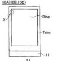
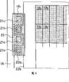
10A~10D:液晶显示装置,11:透明基板,12:扫描线,13:栅绝缘膜,14:半导体层,15:信号线,16:共用布线,17:钝化膜,18:平坦化膜,19、19a、19b:像素电极,20:绝缘膜,21、21a~21c:接触孔,22、22a、22b:共用电极,23:导电通路,24:缝隙,25:框状的缺口部,Disp:显示区域,Trim:边框区域10A~10D: Liquid crystal display device, 11: Transparent substrate, 12: Scanning line, 13: Gate insulating film, 14: Semiconductor layer, 15: Signal line, 16: Common wiring, 17: Passivation film, 18: Planarizing film , 19, 19a, 19b: pixel electrodes, 20: insulating films, 21, 21a-21c: contact holes, 22, 22a, 22b: common electrodes, 23: conductive paths, 24: slits, 25: frame-shaped notches,Disp : Display area, Trim : Border area
具体实施方式Detailed ways
下面,参照附图,通过实施例来说明本发明的最佳实施方式。但是,下面所示的实施例作为用来使本发明的技术构思具体化的液晶显示装置将例示FFS模式的液晶显示装置,并不是将本发明特定为该FFS模式的液晶显示装置之意,同样还能够适用于包括在技术方案的范围内的其他实施方式。Hereinafter, the best mode of carrying out the present invention will be described through examples with reference to the accompanying drawings. However, the embodiments shown below illustrate an FFS-mode liquid crystal display device as a liquid crystal display device for realizing the technical concept of the present invention, and do not intend to specify the present invention as the FFS-mode liquid crystal display device. It can also be applied to other embodiments included in the scope of the technical claims.
实施例1Example 1
作为实施例1的FFS模式的液晶显示装置,将按制造工序顺序使用图1~图5,来说明具有平坦化膜、把上电极连接于共用布线来作为共用电极的FFS模式的液晶显示装置的例子。还有,图1是实施例1的液晶显示装置10A的阵列基板的2个像素的量的模式俯视图。图2是表示实施例1的液晶显示装置的共用布线和共用电极的连接位置X的附图。图3是实施例1的液晶显示装置10A的X部分处的阵列基板的放大俯视图。图4A是沿着图1的IVA-IVA线的模式截面图,图4B是沿着图1的IVB-IVB线的模式截面图,图4C是沿着图3的IVC-IVC线的模式截面图。另外,图5是实施例1的液晶显示装置的变形例中的X部分的阵列基板的放大俯视图。As the FFS mode liquid crystal display device of Example 1, the structure of the FFS mode liquid crystal display device having a flattening film and connecting the upper electrode to the common wiring as a common electrode will be described using FIGS. example. 1 is a schematic plan view of two pixels of the array substrate of the liquid
当制造该实施例1的FFS模式的液晶显示装置10A中的阵列基板AR时,首先在玻璃基板等透明基板11的表面整体的范围内形成金属膜等的导电性层。随后,采用众所周知的光刻法及腐蚀法,在显示区域形成多条扫描线12使之相互平行,并且在显示区域的周围(下面,称为“边框区域”。)形成栅布线(未图示)。该栅布线并不一定作为扫描线用的布线来使用,因为是和扫描线相同材质的布线,所以称为“栅布线”,适合使用于各种的布线用。When manufacturing the array substrate AR in the FFS mode liquid
接下来,在该表面整体覆盖由氮化硅层或氧化硅层构成的栅绝缘膜13。随后,在采用CVD法例如将非晶硅(下面,称为“a-Si”。)层覆盖在栅绝缘膜13的表面整体的范围内之后,同样采用光刻法及腐蚀法,在TFT形成区域形成由a-Si层构成的半导体层14。形成该半导体层14后的位置的扫描线12的区域将形成TFT的栅电极G。Next, the entire surface is covered with a
接下来,将由金属膜构成的导电性层,覆盖在形成半导体层14后的透明基板11的表面整体的范围内。进而,把由该金属膜所构成的导电性层,采用光刻法及腐蚀法在显示区域Disp形成包括源电极S的信号线15并使之与扫描线12正交,在TFT形成区域形成漏电极D,并且在边框区域Trim形成源布线(未图示)及共用布线16。在该共用布线16形成连接部161,该连接部161在与下面所示的和共用电极22a的连接位置X(参见图2)对应的位置处宽度被部分扩大。还有,信号线15的源电极S部分及漏电极D部分全都部分重叠到半导体层14的表面。Next, a conductive layer made of a metal film is covered over the entire surface of the
随后,在通过上述工序所得到的透明基板11的表面整体覆盖钝化膜17。作为该钝化膜17,虽然可以使用由氮化硅层或氧化硅层构成的膜,但是从绝缘性的观点来看,优选的是氮化硅层。进而,在钝化膜17的表面整体依次叠层例如由丙烯酸树脂或聚酰亚胺树脂构成的平坦化膜(也称为层间膜)18及由ITO或IZO构成的透明导电性层。Subsequently, the
接下来,对透明导电性层,采用光刻法及腐蚀法,在每个子像素区域形成像素电极19a。在实施例1的液晶显示装置10A中,该像素电极19a对应于本发明的第1电极。Next, for the transparent conductive layer, a
进而,在形成有像素电极19a后的基板11表面整体的范围内,将由氮化硅层或氧化硅层构成的绝缘膜20形成为预定的厚度。该绝缘膜20作为电介质膜来发挥作用,该电介质膜在像素电极19a和通过后面的工序形成于绝缘膜20表面的透明的共用电极之间形成辅助电容。因此,通过适当调整该绝缘膜的厚度,就可以调整辅助电容的大小使之成为预期的值。Furthermore, an insulating
接下来,从该绝缘膜20的表面,分别同时形成:第1接触孔21a,贯穿绝缘膜20、平坦化膜18及钝化膜17到达共用布线16的连接部161的表面;第2接触孔21b,贯穿绝缘膜20到达像素电极19a的表面;和第3接触孔21c,贯穿绝缘膜20、平坦化膜18及钝化膜17到达漏电极D的表面。在该接触孔21a~21c的形成中,能够采用作为干式腐蚀法的1种的等离子腐蚀法。Next, from the surface of the insulating
接下来,在形成有接触孔21a~21c后的基板11的表面整体的范围内,形成由ITO或IZO构成的透明导电性层。此时,其状态为,利用透明导电性层并通过接触孔21a~21c,共用布线16、像素电极19a及漏电极D相互进行电连接。Next, a transparent conductive layer made of ITO or IZO is formed over the entire surface of the
随后,通过采用光刻法及腐蚀法,对上述透明导电性层进行腐蚀,来形成实质上覆盖显示区域整体的共用电极22a。此时,同时在共用电极22a,在每个子像素区域内相互平行地形成用来使之发生边缘场效应的多条缝隙24,并且在导电通路23的周围设置框状的缺口部25,对导电通路23和共用电极22a进行电绝缘。另外,在该共用电极22a,在共用布线16和共用电极22a的连接位置X形成连接部22a1,使之俯视和共用布线16的、宽度被部分扩大的连接部161重叠。还有,在图3中,缝隙24及框状的缺口部25省略了图示。在实施例1的液晶显示装置10A中,该共用电极22a对应于本发明的第2电极。Thereafter, the above-mentioned transparent conductive layer is etched by photolithography and etching to form the
这样一来,共用电极22a通过第1接触孔21a,和共用布线16进行电连接,像素电极19a经过第2接触孔21b、导电通路23及第3接触孔21c,与TFT的漏电极D进行连接。此后,通过在共用电极22a侧的表面整体设置取向膜(未图示),实施例1的液晶显示装置10A的阵列基板AR就得以完成。In this way, the
与上述阵列基板AR相对向的滤色基板省略了图示,可以使用和以往的FFS模式的液晶显示面板用的滤色基板实质上相同的基板。也就是说,该滤色基板在与各个像素电极相对向的位置形成各色的滤色层,而且,在滤色层的表面设置取向膜。而且,在滤色层和透明基板之间的、与扫描线12及信号线相对向的位置以及与TFT相对向的位置,分别形成黑矩阵。The color filter substrate facing the above-mentioned array substrate AR is omitted from the illustration, and substantially the same color filter substrate as a conventional color filter substrate for an FFS mode liquid crystal display panel can be used. That is, in the color filter substrate, color filter layers of each color are formed at positions facing each pixel electrode, and an alignment film is provided on the surface of the color filter layer. Further, black matrices are formed at positions facing the
特别是为了成为实施例1的液晶显示装置10A用的滤色基板,可以通过在与上述导电通路23或框状缺口部25相对向的位置再设置黑矩阵,遮挡来自该部分的泄漏光。接下来,通过使上述阵列基板及滤色基板分别相对向,并在内部封入液晶,获得实施例1的液晶显示装置10A。In particular, in order to serve as a color filter substrate for the liquid
根据这样制造出的实施例1的液晶显示装置10A,虽然接触孔形成3处,但是因为这些接触孔全部贯穿像素电极19a上的绝缘膜20,所以能够通过一次的工序同时形成3处的接触孔。而且,根据该液晶显示装置10A,因为架桥结构的导电通路23采用和共用电极22a相同的材料来形成,所以能够和共用电极22a的形成同时,通过各接触孔21a~21c实现各像素电极19a和漏电极D之间、共用电极22a和共用布线16之间的电导通。因此,根据实施例1的液晶显示装置10A,能获得一种FFS模式的液晶显示装置10A,不用特别增加制造工时就能够制造,并且在平坦化膜18上形成有像素电极19a及共用电极22a。According to the liquid
另外,根据实施例1的液晶显示装置10A,像素电极19a和共用电极22a之间的绝缘膜20作为形成辅助电容的电介质膜来发挥作用。因此,通过调整该绝缘膜20的厚度,就可以容易调整辅助电容的大小。除此之外,因为电场强度,只要对像素电极19a和共用电极22a之间施加的电压为一定,则与电极间距离成反比例增大,所以若使绝缘膜20的厚度变薄,则像素电极19a和共用电极22a之间的电场强度增强。因此,若使绝缘膜20的厚度变薄,则即便降低对像素电极19a和共用电极22a之间施加的电压,也可以获得用来驱动液晶分子的预定的电场强度。从而,根据实施例1的液晶显示装置10A,能获得一种液晶显示装置10A,可以使显示质量得到提高并且进行低电压驱动,还可以谋求低消耗功率化。In addition, according to the liquid
而且,根据实施例1的液晶显示装置10A,因为TFT等的表面由平坦化膜覆盖,所以在共用电极22a不产生以往例的FFS模式的液晶显示装置的那种台阶差。因此,根据实施例1的液晶显示装置10A,未图示的滤色基板和共用电极22a之间的间隔,也就是单元间隙均匀,并且因为在显示区域内由黑矩阵遮光的区域的面积减少,所以开口率增大。从而,根据实施例1的液晶显示装置10A,能获得一种FFS模式的液晶显示装置10A,可以作为明亮、显示画质良好且被小型化及高精细化的液晶显示装置来适当使用。Furthermore, according to the liquid
实施例2Example 2
下面,将按制造工序顺序使用图6~图9,来说明具有平坦化膜、把下电极连接于共用布线来作为共用电极的实施例2的FFS模式的液晶显示装置的例子。还有,图6是实施例2的液晶显示装置的阵列基板的2个像素的量的模式俯视图。图7是表示实施例2的液晶显示装置的共用布线和共用电极的连接位置处的阵列基板的放大俯视图。图8A是沿着图6的VIIIA-VIIIA线的模式截面图,图8B是沿着图7的VIIIB-VIIIB线的模式截面图。另外,图9是实施例2的液晶显示装置10B的变形例中的、和共用电极的连接位置的阵列基板的放大俯视图。还有,实施例2的液晶显示装置10B中共用布线与共用电极的连接位置由于和图2所示的实施例1的液晶显示装置10A的共用布线与共用电极的连接位置X相同,因而将根据需要,引用图2进行说明。Next, an example of the FFS mode liquid crystal display device of the second embodiment having a flattening film and connecting the lower electrode to the common wiring as the common electrode will be described using FIGS. 6 to 9 in the order of the manufacturing steps. 6 is a schematic plan view of two pixels of the array substrate of the liquid crystal display device according to the second embodiment. 7 is an enlarged plan view showing the array substrate at the connection position of the common wiring and the common electrode in the liquid crystal display device of the second embodiment. 8A is a schematic cross-sectional view along line VIIIA-VIIIA of FIG. 6 , and FIG. 8B is a schematic cross-sectional view along line VIIIB-VIIIB of FIG. 7 . 9 is an enlarged plan view of the array substrate at the connection position to the common electrode in a modified example of the liquid
该实施例2的FFS模式的液晶显示装置10B的阵列基板AR由于在透明基板11的表面形成扫描线12、栅绝缘膜13、半导体层14、包括源电极S的信号线15、漏电极D、源布线、共用布线16及其连接部161、钝化膜17以及平坦化膜18的工序和实施例1的FFS模式的液晶显示装置10A的阵列基板AR的制造方法实质上相同,因而其详细的说明予以省略。The array substrate AR of the FFS mode liquid
在形成平坦化膜18之后,在平坦化膜18的表面整体的范围内形成由ITO或IZO构成的透明导电性层,并采用光刻法及腐蚀法将共用电极22b形成为预定的图形。在该共用电极22b,在共用布线16和共用电极22b的连接位置X(参见图2)形成连接部22b1,使之俯视不和共用布线16及其连接部161重叠,而其位置为与共用布线16及其连接部161相邻。另外,同时在共用电极22b的下面所述的第1接触孔21a的形成位置,形成比第1接触孔21a稍大的孔。在实施例2的液晶显示装置10B中,该共用电极22b对应于本发明的第1电极。还有,在图7中,缝隙24省略了图示。After the
接下来,在形成有共用电极22b后的基板11的表面整体的范围内将由氮化硅层或氧化硅层构成的绝缘膜20形成为预定厚度。此时,将比共用电极22b中所形成的第1接触孔21a的大小大的孔内用绝缘膜20来充填。接下来,从该绝缘膜20的表面,分别同时形成:第1接触孔21a,贯穿绝缘膜20、平坦化膜18及钝化膜17到达漏电极D的表面;第2接触孔21b,贯穿绝缘膜20到达共用电极22b的表面;和第3接触孔21c,贯穿绝缘膜20、平坦化膜18及钝化膜17到达共用布线16的连接部161表面。此时,共用电极22b不露出于接触孔21a的周边壁。在该接触孔21a~21c的形成中,能够采用作为干式腐蚀法1种的等离子腐蚀法。Next, the insulating
接下来,在形成有接触孔21a~21c后的基板11的表面整体的范围内,形成由ITO或IZO构成的透明导电性层。此时,其状态为,利用透明导电性层并通过接触孔21a~21c,将共用布线16、像素电极19b及漏电极D相互进行电连接。Next, a transparent conductive layer made of ITO or IZO is formed over the entire surface of the
随后,通过采用光刻法及腐蚀法,在每个子像素区域形成像素电极19b。此时,同时在各像素电极19b,平行形成用来使之发生边缘场效应的多条缝隙24,并且去除导电通路23周围的透明导电性层,以在连接位置X形成导电通路23。由于成为这种结构,因而能确保导电通路23和各像素电极19b之间的绝缘性。在实施例2的液晶显示装置10B中,该各像素电极19b对应于本发明的第2电极。Subsequently, a
这样一来,各像素电极19b就通过第1接触孔21a,和漏电极D进行电连接,共用电极22b经过第2接触孔21b、导电通路23及第3接触孔21c,与共用布线16进行连接。此后,通过在共用电极22b侧的表面整体设置取向膜(未图示),实施例2的液晶显示装置10B的阵列基板AR就得以完成。此后的制造工序由于和实施例1的液晶显示装置10A的制造工序相同,因而省略详细的说明。In this way, each
根据这样制造出的实施例2的液晶显示装置10B,虽然接触孔形成3处,但是因为这些接触孔全部贯穿共用电极22b上的绝缘膜20,所以能够通过一次的工序同时形成3处的接触孔。而且,根据该液晶显示装置10B,因为架桥结构的导电通路23采用和像素电极19b相同的材料来形成,所以能够和像素电极19b的形成同时,通过各接触孔21a~21c实现各像素电极19b和漏电极D之间、共用电极22b和共用布线16之间的电导通。因此,根据实施例2的液晶显示装置10B,能获得一种FFS模式的液晶显示装置10B,不用特别增加制造工时就能够制造,并且在平坦化膜18上形成有像素电极19b及共用电极22b。还有,其他实施例2的液晶显示装置10B的作用、效果由于和实施例1的液晶显示装置的情形相同,因而其详细说明予以省略。According to the liquid
比较例1Comparative example 1
下面,为了确认本发明的液晶显示装置的效果,作为比较例1的FFS模式的液晶显示装置,按制造工序顺序使用图10及图11来说明不具备平坦化膜的FFS模式的液晶显示装置的例子。还有,图10是比较例1的FFS模式的液晶显示装置的阵列基板的2个像素的量的概略俯视图,图11A是沿着图10的XIA-XIA线的概略截面图,图11b是沿着图10的XIB-XIB线的概略截面图。还有,在图10及图11中,对和图1~图5所示的实施例1的液晶显示装置相同的结构部分,附上相同的参照符号进行说明。Next, in order to confirm the effect of the liquid crystal display device of the present invention, as the liquid crystal display device of the FFS mode of Comparative Example 1, the liquid crystal display device of the FFS mode that does not have a planarizing film will be described in the order of manufacturing steps using FIGS. 10 and 11 . example. Also, FIG. 10 is a schematic plan view of two pixels of the array substrate of the FFS mode liquid crystal display device of Comparative Example 1, and FIG. 11A is a schematic cross-sectional view along line XIA-XIA of FIG. 10 , and FIG. A schematic cross-sectional view along line XIB-XIB of FIG. 10 is shown. In FIGS. 10 and 11, the same components as those of the liquid crystal display device of Embodiment 1 shown in FIGS. 1 to 5 are described with the same reference numerals.
该比较例1的FFS模式的液晶显示装置10C的阵列基板AR在玻璃基板等透明基板11的表面整体的范围内,下部形成金属膜等的导电性层之后,采用光刻法及腐蚀法,形成具有栅部分的多条扫描线12及多条共用布线16使之相互平行。The array substrate AR of the FFS-mode liquid crystal display device 10C of Comparative Example 1 is formed on the lower portion of the entire surface of the
接下来,在形成有扫描线12及共用布线16后的透明基板11的表面整体的范围内,覆盖例如由ITO或IZO构成的透明导电性层,并同样采用光刻法及腐蚀法来形成共用电极22。该共用电极22虽然和共用布线16进行电连接,但是未和扫描线12或栅电极G连接。Next, within the entire range of the surface of the
进而,在该表面整体覆盖由氮化硅层或氧化硅层构成的栅绝缘膜13,接下来在采用CVD法例如将a-Si层覆盖在栅绝缘膜13的表面整体的范围内之后,同样采用光刻法及腐蚀法,在TFT形成区域形成由a-Si层构成的半导体层14。形成该半导体层14的位置的扫描线12的区域将形成TFT的栅电极G。Furthermore, the entire surface is covered with a
接下来,将由金属膜等构成的导电性层覆盖在形成有半导体层14后的透明基板11表面整体的范围内,同样采用光刻法及腐蚀法,形成包括源电极S的信号线15及漏电极D。该信号线15的源电极S部分及漏电极D部分全都部分重叠到半导体层14的表面。进而,在该基板的表面整体覆盖由氮化硅层构成的钝化膜17。Next, a conductive layer made of a metal film or the like is covered on the entire surface of the
接下来,在与漏电极D对应的位置的钝化膜17形成接触孔21,使漏电极D的一部分露出。进而,在该表面整体的范围内覆盖例如由ITO或IZO构成的透明导电性层。此时,漏电极D的状态为,通过接触孔21,和透明导电性层进行电连接。接下来,采用光刻法及腐蚀法,在由信号线15所包围的每个区域各自的钝化膜17上形成下述像素电极19使之成为图10所示的图形,该像素电极19相互平行形成有多条缝隙24。在该状态下,各个像素电极19通过接触孔21,和漏电极D进行电连接。Next, a
此后,通过在像素电极19侧的表面整体设置取向膜(未图示),比较例1的液晶显示装置10C的阵列基板AR就得以完成。此后的制造工序由于和实施例1的液晶显示装置10A的制造工序相同,因而省略详细的说明。Thereafter, the array substrate AR of the liquid crystal display device 10C of Comparative Example 1 is completed by providing an alignment film (not shown) on the entire surface of the
这种结构的比较例1的液晶显示装置10C因为共用电极22和共用布线16直接连接,所以接触孔21只需要1处,但是在共用布线16的旁边在像素电极19的一部分产生台阶差,另外TFT的表面成为凹凸状态。因此,该比较例1的液晶显示装置10C由于在滤色基板不只是在与TFT相对向的部分,还需要在与台阶差部相对向的部分设置黑矩阵进行遮光,因而至少按该台阶差部的量使开口率下降。In the liquid crystal display device 10C of Comparative Example 1 having such a structure, since the
除此之外,因为由遮光性材料构成的共用布线16在扫描线12间被平行配置,所以还因该共用布线16而使开口率下降。因此,比较例1的液晶显示装置10C和实施例1及2的液晶显示装置10A及10B相比,开口率必然下降。In addition, since the
比较例2Comparative example 2
下面,为了确认本发明的效果,作为比较例2,按制造工序顺序使用图12~图14来说明具备平坦化膜的FFS模式液晶显示装置的例子。还有,图12是比较例2的液晶显示装置的阵列基板的2个像素的量的模式俯视图。图13是比较例2的液晶显示装置的X部分处的阵列基板的放大俯视图。图14A是沿着图12的XIVA-XIVA线的概略截面图,图14B是沿着图13的XIVB-XIVB线的概略截面图。还有,在图12~图14中,对于和图1~图3所示的实施例1的FFS模式的液晶显示装置10A相同的结构部分,附上相同的参照符号,其详细的说明予以省略。另外,比较例2的液晶显示装置中共用布线与共用电极的连接位置由于和图2所示实施例1的液晶显示装置10A的共用布线与共用电极的连接位置X相同,因而将根据需要,引用图2进行说明。Next, in order to confirm the effects of the present invention, as Comparative Example 2, an example of an FFS mode liquid crystal display device including a planarizing film will be described using FIGS. 12 to 14 in order of manufacturing steps. 12 is a schematic plan view of two pixels of the array substrate of the liquid crystal display device of Comparative Example 2. As shown in FIG. FIG. 13 is an enlarged plan view of the array substrate at part X of the liquid crystal display device of Comparative Example 2. FIG. 14A is a schematic cross-sectional view taken along line XIVA-XIVA of FIG. 12 , and FIG. 14B is a schematic cross-sectional view taken along line XIVB-XIVB of FIG. 13 . In FIGS. 12 to 14, the same components as those of the FFS-mode liquid
该比较例2的FFS模式的液晶显示装置10D的阵列基板AR制造工序之中,在透明基板11的表面形成包括栅电极G的扫描线12、栅绝缘膜13、半导体层14、包括源电极S的信号线15、漏电极D、源布线、共用布线16及其连接部161、钝化膜17及平坦化膜18的工序,由于和实施例1的FFS模式的液晶显示装置10A的阵列基板AR的制造工序实质上相同,因而其详细的说明予以省略。In the manufacturing process of the array substrate AR of the FFS mode liquid
在形成平坦化膜18之后,在下面所述的共用电极22和共用布线16的连接位置X(参见图2),使之贯穿连接部161上的平坦化膜18及钝化膜17地形成第1接触孔21a,使连接部161的表面露出。接下来,在形成有该平坦化膜18后的透明基板11的表面整体的范围内形成由ITO或IZO构成的透明导电性层,采用光刻法及腐蚀法,将共用电极22形成为预定的图形。与此同时,在下面所示的第2接触孔21b的形成位置,形成比该第2接触孔21b的大小大的孔。此时,其状态为,共用电极22和共用布线16的连接部161通过第1接触孔21a内的透明导电性层进行电连接。After the
接下来,在形成有共用电极22后的基板11的表面整体的范围内,将由氮化硅层或氧化硅层构成的绝缘膜20形成为预定厚度。此时,将比在共用电极22所形成的第2接触孔21b的大小大的孔内用绝缘膜20来充填。进而,从该绝缘膜20的表面形成第2接触孔21b,贯穿绝缘膜20、平坦化膜18及钝化膜17到达漏电极D的表面。此时,共用电极22不露出于接触孔21b的周边壁。Next, an insulating
接下来,在形成有第2接触孔21b后的基板11表面整体的范围内,形成由ITO或IZO构成的透明导电性层。此时,其状态为,透明导电性层通过第2接触孔21b,和漏电极D进行电连接。Next, a transparent conductive layer made of ITO or IZO is formed over the entire surface of the
随后,采用光刻法及腐蚀法,在每个子像素区域形成预定图形的像素电极19。此时,同时在各像素电极19,平行形成用来使之发生边缘场效应的多条缝隙24。这样一来,其状态为,各像素电极19通过第2接触孔21b,和漏电极D进行电连接。Subsequently, a photolithography method and an etching method are used to form a
此后,通过在像素电极19侧的表面整体设置取向膜(未图示),比较例2的液晶显示装置10D的阵列基板AR就得以完成。此后的制造工序由于和实施例1的液晶显示装置10A的制造工序相同,因而省略详细的说明。Thereafter, by providing an alignment film (not shown) on the entire surface of the
这样制造所得的比较例2的FFS模式的液晶显示装置10D实质上具备和实施例1及2的FFS模式的液晶显示装置10A及10B相同的光学特性。但是,在该比较例2的液晶显示装置10D中,接触孔存在2处,该2处的接触孔却分别需要通过不同的工序来形成。因此,可知:为了制造比较例2的FFS模式的液晶显示装置10D,和制造实施例1及2的液晶显示装置10A及10B的工序相比,接触孔的制造工序增加了一个工序。The thus-produced FFS-mode liquid
还有,在实施例1及2中,虽然作为设置于像素电极19的缝隙24表示出长度方向的两端闭合的形状的例子,但是可以将缝隙形成为一方端侧开放的形状。这种情况下,由于可以直到该缝隙开放的一方侧的端部都使之发挥边缘效应,而且该缝隙的端部开放的一侧的液晶分子取向紊乱较少,因而若和缝隙的两端侧闭合的液晶显示装置相比,则必须利用在滤色基板所设置的黑矩阵进行遮光的部分的面积减少,因此能获得显示开口率较大并且显示明亮的液晶显示装置。Also, in Embodiments 1 and 2, the
Claims (8)
Translated fromChineseApplications Claiming Priority (2)
| Application Number | Priority Date | Filing Date | Title |
|---|---|---|---|
| JP2007014660AJP4356750B2 (en) | 2007-01-25 | 2007-01-25 | Liquid crystal display device and manufacturing method thereof |
| JP014660/2007 | 2007-01-25 |
Publications (2)
| Publication Number | Publication Date |
|---|---|
| CN101231437Atrue CN101231437A (en) | 2008-07-30 |
| CN101231437B CN101231437B (en) | 2011-04-06 |
Family
ID=39667542
Family Applications (1)
| Application Number | Title | Priority Date | Filing Date |
|---|---|---|---|
| CN2008100039468AActiveCN101231437B (en) | 2007-01-25 | 2008-01-23 | Liquid crystal display device and method of manufacturing the same |
Country Status (5)
| Country | Link |
|---|---|
| US (1) | US7636144B2 (en) |
| JP (1) | JP4356750B2 (en) |
| KR (1) | KR100917503B1 (en) |
| CN (1) | CN101231437B (en) |
| TW (1) | TW200835993A (en) |
Cited By (4)
| Publication number | Priority date | Publication date | Assignee | Title |
|---|---|---|---|---|
| CN102810571A (en)* | 2012-08-13 | 2012-12-05 | 京东方科技集团股份有限公司 | A substrate, a display device, and a method for preparing the substrate |
| CN103713435A (en)* | 2013-09-16 | 2014-04-09 | 友达光电股份有限公司 | Pixel structure, manufacturing method thereof, and display panel |
| CN105242467A (en)* | 2012-03-26 | 2016-01-13 | 乐金显示有限公司 | Display device and method for manufacturing the same |
| CN105259714A (en)* | 2009-12-11 | 2016-01-20 | 乐金显示有限公司 | Liquid crystal display device |
Families Citing this family (41)
| Publication number | Priority date | Publication date | Assignee | Title |
|---|---|---|---|---|
| KR101189275B1 (en) | 2005-08-26 | 2012-10-09 | 삼성디스플레이 주식회사 | Thin film transistor array panel and method for manufacturing the same |
| US7903220B2 (en)* | 2007-10-01 | 2011-03-08 | Sony Corporation | Liquid crystal display device and electronic apparatus |
| KR101528758B1 (en)* | 2008-07-08 | 2015-06-15 | 삼성디스플레이 주식회사 | Method of driving a liquid crystal display apparatus, array substrate, method of manufacturing the array substrate and liquid crystal display apparatus having the same |
| JP5121651B2 (en)* | 2008-09-29 | 2013-01-16 | 株式会社ジャパンディスプレイウェスト | Liquid crystal display device and electronic device |
| JP5500712B2 (en)* | 2009-09-02 | 2014-05-21 | 株式会社ジャパンディスプレイ | LCD panel |
| JP5404281B2 (en) | 2009-09-28 | 2014-01-29 | 株式会社ジャパンディスプレイ | LCD panel |
| KR101250319B1 (en)* | 2009-10-06 | 2013-04-03 | 엘지디스플레이 주식회사 | Fringe field switching mode liquid crystal display device and Method of fabricating the same |
| WO2011043194A1 (en) | 2009-10-09 | 2011-04-14 | Semiconductor Energy Laboratory Co., Ltd. | Semiconductor device and method for manufacturing the same |
| JP2011095451A (en)* | 2009-10-29 | 2011-05-12 | Sony Corp | In-plane switching liquid crystal display device |
| JP5280988B2 (en)* | 2009-11-09 | 2013-09-04 | 株式会社ジャパンディスプレイ | Manufacturing method of liquid crystal display device |
| JP4911793B2 (en) | 2009-11-09 | 2012-04-04 | 東芝モバイルディスプレイ株式会社 | Liquid crystal display |
| JP5585127B2 (en)* | 2010-03-08 | 2014-09-10 | 三菱電機株式会社 | Array substrate and liquid crystal display device |
| CN102135691B (en)* | 2010-09-17 | 2012-05-23 | 京东方科技集团股份有限公司 | Array substrate, manufacturing method thereof and liquid crystal display |
| GB2489939A (en)* | 2011-04-11 | 2012-10-17 | Plastic Logic Ltd | Control of capacitive coupling in pixel circuitry |
| CN102629047B (en)* | 2011-07-12 | 2014-10-08 | 京东方科技集团股份有限公司 | Pixel unit, array substrate, liquid crystal panel and display equipment |
| JP5939755B2 (en)* | 2011-09-07 | 2016-06-22 | 株式会社ジャパンディスプレイ | Liquid crystal display |
| KR101873498B1 (en)* | 2011-10-07 | 2018-07-03 | 삼성디스플레이 주식회사 | Liquid crystal display device |
| US8773627B2 (en)* | 2011-10-07 | 2014-07-08 | Japan Display West Inc. | Liquid crystal display device and method for manufacturing liquid crystal display device |
| WO2013073619A1 (en)* | 2011-11-18 | 2013-05-23 | シャープ株式会社 | Semiconductor device, display device, and method for producing semiconductor device |
| MY173293A (en) | 2012-02-15 | 2020-01-13 | Sharp Kk | Liquid crystal display |
| US9368523B2 (en)* | 2012-03-27 | 2016-06-14 | Sharp Kabushiki Kaisha | Semiconductor device, method for manufacturing semiconductor device, and display device |
| TWI465819B (en)* | 2012-07-13 | 2014-12-21 | Au Optronics Corp | Liquid crystal display panel |
| US20140034952A1 (en)* | 2012-07-31 | 2014-02-06 | Shenzhen China Star Optoelectronics Technology Co. Ltd. | Liquid Crystal Display Device, Array Substrate and Manufacturing Method Thereof |
| TWI636309B (en)* | 2013-07-25 | 2018-09-21 | 日商半導體能源研究所股份有限公司 | Liquid crystal display device and electronic device |
| JP6188473B2 (en) | 2013-07-31 | 2017-08-30 | 三菱電機株式会社 | Thin film transistor array substrate and manufacturing method thereof |
| KR102118332B1 (en) | 2013-08-12 | 2020-06-04 | 삼성디스플레이 주식회사 | Display substrate and method of manufacturing the same |
| JP2015049426A (en) | 2013-09-03 | 2015-03-16 | パナソニック液晶ディスプレイ株式会社 | Liquid crystal display device |
| JP5800070B2 (en)* | 2014-07-15 | 2015-10-28 | 三菱電機株式会社 | Array substrate and liquid crystal display device |
| CN104157613B (en)* | 2014-07-31 | 2017-03-08 | 京东方科技集团股份有限公司 | A kind of preparation method of array base palte |
| CN104571765B (en)* | 2015-01-09 | 2017-08-29 | 京东方科技集团股份有限公司 | A kind of In-cell touch panel and display device |
| WO2016194269A1 (en) | 2015-05-29 | 2016-12-08 | パナソニック液晶ディスプレイ株式会社 | Liquid crystal display device |
| WO2016194270A1 (en) | 2015-05-29 | 2016-12-08 | パナソニック液晶ディスプレイ株式会社 | Liquid crystal display device |
| KR102263876B1 (en)* | 2015-05-29 | 2021-06-14 | 엘지디스플레이 주식회사 | In cell touch liquid crystal display device and method for manufacturing the same |
| TWI590424B (en)* | 2016-03-14 | 2017-07-01 | 友達光電股份有限公司 | Pixel structure |
| JP2017173624A (en) | 2016-03-24 | 2017-09-28 | パナソニック液晶ディスプレイ株式会社 | Liquid crystal display device |
| JP6936750B2 (en) | 2018-02-23 | 2021-09-22 | パナソニック液晶ディスプレイ株式会社 | Liquid crystal display |
| JP7030563B2 (en) | 2018-03-02 | 2022-03-07 | 株式会社ジャパンディスプレイ | Display device |
| KR101888035B1 (en)* | 2018-03-05 | 2018-08-13 | 엘지디스플레이 주식회사 | Method for fabricating array substratefor fringe field switching mode liquid crystal display device |
| CN208488633U (en)* | 2018-05-14 | 2019-02-12 | 北京京东方技术开发有限公司 | Array substrate, display panel and display device |
| CN109324720B (en)* | 2018-09-28 | 2023-09-26 | 武汉华星光电技术有限公司 | Array substrate, touch display screen and driving method of array substrate |
| CN115424538B (en)* | 2022-09-09 | 2024-04-09 | 惠科股份有限公司 | Display device and method for manufacturing the same |
Family Cites Families (12)
| Publication number | Priority date | Publication date | Assignee | Title |
|---|---|---|---|---|
| TW460731B (en)* | 1999-09-03 | 2001-10-21 | Ind Tech Res Inst | Electrode structure and production method of wide viewing angle LCD |
| KR100325079B1 (en) | 1999-12-22 | 2002-03-02 | 주식회사 현대 디스플레이 테크놀로지 | Method of manufacturing lcd having high aperture ratio and high transmittance |
| JP3832261B2 (en)* | 2000-03-16 | 2006-10-11 | セイコーエプソン株式会社 | Liquid crystal device, projection display device, and electronic apparatus |
| KR20020002052A (en)* | 2000-06-29 | 2002-01-09 | 주식회사 현대 디스플레이 테크놀로지 | Method for manufacturing fringe field switching mode lcd |
| KR100482468B1 (en) | 2000-10-10 | 2005-04-14 | 비오이 하이디스 테크놀로지 주식회사 | Fringe field switching mode lcd |
| JP3949897B2 (en)* | 2001-01-29 | 2007-07-25 | 株式会社日立製作所 | Liquid crystal display |
| JP4305811B2 (en)* | 2001-10-15 | 2009-07-29 | 株式会社日立製作所 | Liquid crystal display device, image display device and manufacturing method thereof |
| US6650385B1 (en)* | 2002-04-24 | 2003-11-18 | Prime View International Co., Ltd. | Scattering fringe field optical-compensated reflective and transflective liquid crystal display |
| JP4627148B2 (en)* | 2004-04-09 | 2011-02-09 | 株式会社 日立ディスプレイズ | Display device |
| JP4223993B2 (en)* | 2004-05-25 | 2009-02-12 | 株式会社 日立ディスプレイズ | Liquid crystal display |
| JP4223992B2 (en)* | 2004-05-25 | 2009-02-12 | 株式会社 日立ディスプレイズ | Liquid crystal display |
| KR20060001165A (en) | 2004-06-30 | 2006-01-06 | 엘지.필립스 엘시디 주식회사 | Horizontal field applied thin film transistor substrate and manufacturing method thereof |
- 2007
- 2007-01-25JPJP2007014660Apatent/JP4356750B2/enactiveActive
- 2008
- 2008-01-22TWTW097102294Apatent/TW200835993A/enunknown
- 2008-01-22USUS12/009,785patent/US7636144B2/enactiveActive
- 2008-01-23CNCN2008100039468Apatent/CN101231437B/enactiveActive
- 2008-01-24KRKR1020080007710Apatent/KR100917503B1/enactiveActive
Cited By (7)
| Publication number | Priority date | Publication date | Assignee | Title |
|---|---|---|---|---|
| CN105259714A (en)* | 2009-12-11 | 2016-01-20 | 乐金显示有限公司 | Liquid crystal display device |
| CN105242467A (en)* | 2012-03-26 | 2016-01-13 | 乐金显示有限公司 | Display device and method for manufacturing the same |
| CN105242467B (en)* | 2012-03-26 | 2018-08-24 | 乐金显示有限公司 | Display device and its manufacturing method |
| CN102810571A (en)* | 2012-08-13 | 2012-12-05 | 京东方科技集团股份有限公司 | A substrate, a display device, and a method for preparing the substrate |
| CN102810571B (en)* | 2012-08-13 | 2015-03-11 | 京东方科技集团股份有限公司 | Substrate, display device and substrate preparation method |
| CN103713435A (en)* | 2013-09-16 | 2014-04-09 | 友达光电股份有限公司 | Pixel structure, manufacturing method thereof, and display panel |
| CN103713435B (en)* | 2013-09-16 | 2016-05-11 | 友达光电股份有限公司 | Pixel structure, manufacturing method thereof and display panel |
Also Published As
| Publication number | Publication date |
|---|---|
| TWI369560B (en) | 2012-08-01 |
| KR20080070563A (en) | 2008-07-30 |
| KR100917503B1 (en) | 2009-09-16 |
| US7636144B2 (en) | 2009-12-22 |
| CN101231437B (en) | 2011-04-06 |
| JP2008180928A (en) | 2008-08-07 |
| JP4356750B2 (en) | 2009-11-04 |
| US20080180622A1 (en) | 2008-07-31 |
| TW200835993A (en) | 2008-09-01 |
Similar Documents
| Publication | Publication Date | Title |
|---|---|---|
| CN101231437A (en) | Liquid crystal display device and method of manufacturing the same | |
| CN101359139B (en) | Liquid crystal display panel and manufacturing method thereof | |
| CN1908789B (en) | Liquid crystal display device | |
| US7663723B2 (en) | In-plane switching mode liquid crystal display device and fabrication method thereof | |
| CN103309093B (en) | Liquid crystal indicator | |
| US6762815B2 (en) | In-plane switching LCD with a redundancy structure for an opened common electrode and a high storage capacitance | |
| JP2004325953A (en) | Liquid crystal display | |
| US8576365B2 (en) | Display panel | |
| JP2009128905A (en) | Liquid crystal display device | |
| JPH0736058A (en) | Active matrix liquid crystal display | |
| CN102236229A (en) | Array substrate for in-plane switching mode liquid crystal display device | |
| JP2007279634A (en) | Horizontal electric field type liquid crystal display device | |
| CN104813386A (en) | Tft substrate | |
| CN104115058A (en) | Liquid crystal display device with a light guide plate | |
| JP5171412B2 (en) | Liquid crystal display device and electronic device | |
| CN100417992C (en) | liquid crystal display device | |
| CN103309100A (en) | Liquid crystal display device and method of fabricating the same | |
| US20090284695A1 (en) | Liquid crystal display | |
| US20120113372A1 (en) | Liquid crystal display panel | |
| JP2003107508A (en) | Multi-domain vertical alignment type liquid crystal display | |
| JP2004361946A (en) | Liquid crystal display | |
| JP5207947B2 (en) | Liquid crystal display device and manufacturing method thereof | |
| KR20080100642A (en) | Liquid crystal display | |
| WO2014034786A1 (en) | Active matrix substrate and liquid crystal display device | |
| JP2008134498A (en) | Liquid crystal display panel and method for manufacturing the same |
Legal Events
| Date | Code | Title | Description |
|---|---|---|---|
| C06 | Publication | ||
| PB01 | Publication | ||
| C10 | Entry into substantive examination | ||
| SE01 | Entry into force of request for substantive examination | ||
| ASS | Succession or assignment of patent right | Owner name:NANKAI UNIVERSITY Free format text:FORMER OWNER: SANYO EPSON IMAGING DEVICES CO. Effective date:20100727 | |
| C41 | Transfer of patent application or patent right or utility model | ||
| COR | Change of bibliographic data | Free format text:CORRECT: ADDRESS; FROM: NAGANO PREFECTURE, JAPAN TO: TOKYO, JAPAN | |
| TA01 | Transfer of patent application right | Effective date of registration:20100727 Address after:Tokyo, Japan Applicant after:Sony Corp. Address before:Nagano Applicant before:Epson Imaging Devices Corp. | |
| C14 | Grant of patent or utility model | ||
| GR01 | Patent grant | ||
| ASS | Succession or assignment of patent right | Owner name:NIPPON DISPLAY CO., LTD. Free format text:FORMER OWNER: SONY CORPORATION Effective date:20121122 | |
| C41 | Transfer of patent application or patent right or utility model | ||
| TR01 | Transfer of patent right | Effective date of registration:20121122 Address after:Aichi Prefecture, Japan Patentee after:Japan display West Co.,Ltd. Address before:Tokyo, Japan Patentee before:Sony Corp. | |
| TR01 | Transfer of patent right | ||
| TR01 | Transfer of patent right | Effective date of registration:20211021 Address after:Tokyo, Japan Patentee after:JAPAN DISPLAY Inc. Address before:Aichi Prefecture, Japan Patentee before:Japan display West Co.,Ltd. | |
| TR01 | Transfer of patent right | Effective date of registration:20250813 Address after:Tokyo, Japan Patentee after:Magno Haote Co.,Ltd. Country or region after:Japan Address before:Tokyo, Japan Patentee before:JAPAN DISPLAY Inc. Country or region before:Japan |