CN101231193B - Monolithic Visible/Infrared Dual Spectrum Focal Plane Detector - Google Patents
Monolithic Visible/Infrared Dual Spectrum Focal Plane DetectorDownload PDFInfo
- Publication number
- CN101231193B CN101231193BCN2008100693419ACN200810069341ACN101231193BCN 101231193 BCN101231193 BCN 101231193BCN 2008100693419 ACN2008100693419 ACN 2008100693419ACN 200810069341 ACN200810069341 ACN 200810069341ACN 101231193 BCN101231193 BCN 101231193B
- Authority
- CN
- China
- Prior art keywords
- visible light
- infrared
- pixel
- diode
- focal plane
- Prior art date
- Legal status (The legal status is an assumption and is not a legal conclusion. Google has not performed a legal analysis and makes no representation as to the accuracy of the status listed.)
- Expired - Fee Related
Links
Images


Landscapes
- Transforming Light Signals Into Electric Signals (AREA)
- Solid State Image Pick-Up Elements (AREA)
Abstract
Translated fromChinese
Description
Translated fromChinese技术领域technical field
本发明涉及一种探测器,尤其涉及一种单片式可见光/红外光双光谱焦平面探测器。The invention relates to a detector, in particular to a single-chip visible light/infrared light dual-spectrum focal plane detector.
背景技术Background technique
目前可见光/红外摄像系统大都采用可见光和红外两种探测器的分离式系统,即以可见光电荷耦合器件(CCD)为基础的可见光探测部分和以红外焦平面为基础的红外光探测部分。At present, most visible light/infrared camera systems use a separate system of visible light and infrared detectors, that is, the visible light detection part based on the visible light charge-coupled device (CCD) and the infrared light detection part based on the infrared focal plane.
上述的分离式摄像系统工作过程如下:当系统对目标进行探测时,可见光探测系统和红外探测系统同时对目标进行成像,在相应的探测系统中可以观测到相应可见光或红外的像;而后端的信号处理系统则可以对前端探测到的可见光和红外信号进行融合处理,得到双波段信号融合的图像,以提高探测器的探测能力。The working process of the above-mentioned separate camera system is as follows: when the system detects the target, the visible light detection system and the infrared detection system simultaneously image the target, and the corresponding visible light or infrared image can be observed in the corresponding detection system; and the signal at the back end The processing system can perform fusion processing on the visible light and infrared signals detected by the front end to obtain a dual-band signal fusion image to improve the detection capability of the detector.
由于整个探测器是通过两个不同的光路系统对目标进行探测,对同一目标,其探测位置不可能做到完全一致,因此所成的可见光像和红外像就会存在一定的位置偏差。由于这种位置偏差的影响,两幅图像不可能完全重合,这就会影响到信号融合后的图像的清晰度。Since the entire detector detects the target through two different optical path systems, the detection positions of the same target cannot be completely consistent, so there will be a certain position deviation between the visible light image and the infrared image formed. Due to the influence of this positional deviation, it is impossible for the two images to overlap completely, which will affect the clarity of the image after signal fusion.
基于上述现有技术中的不足,本发明提出了一种可以解决上述问题的新的单片式可见光/红外光双光谱焦平面探测器。Based on the deficiencies in the prior art above, the present invention proposes a new monolithic visible light/infrared light dual-spectrum focal plane detector that can solve the above problems.
发明内容Contents of the invention
针对现有技术中的不足,本发明提供了一种只需一个光路系统就可成像的单片式可见光/红外光双光谱焦平面探测器。Aiming at the deficiencies in the prior art, the present invention provides a single-chip visible light/infrared light dual-spectrum focal plane detector capable of imaging with only one optical path system.
本发明的技术方案为:它包括:可见光像元、可见光像元收集二极管、红外感光像元、红外感光像元收集二极管、四相CCD转移栅上的电极V1、V2、V3、V4,各个电极按上述顺序从上至下排列并构成CCD信道;可见光像元和红外感光像元并列在四相CCD转移栅的一侧,且可见光像元和红外感光像元的位置可互换;可见光像元和红外感光像元分别通过可见光像元收集二极管和红外感光像元收集二极管把可见光信号和红外信号输入四相CCD转移栅上的相应电极;各个器件间用沟阻隔离,防止信号间的相互干扰。The technical scheme of the present invention is: it comprises: the electrode V1, V2, V3, V4 on the transfer grid of four-phase CCD, each electrode Arranged from top to bottom in the above order to form a CCD channel; visible light pixels and infrared photosensitive pixels are juxtaposed on one side of the four-phase CCD transfer grid, and the positions of visible light pixels and infrared photosensitive pixels are interchangeable; visible light pixels The visible light signal and infrared signal are input to the corresponding electrodes on the four-phase CCD transfer grid through the visible light pixel collection diode and the infrared photosensitive pixel collection diode respectively; each device is isolated by trench resistance to prevent mutual interference between signals .
可见光像元收集二极管把可见光信号输出到电极V1,红外感光像元收集二极管把红外信号输出到电极V3;或者红外感光像元收集二极管把红外信号输出到电极V1,可见光像元收集二极管把可见光信号输出到电极V3。The visible light pixel collection diode outputs the visible light signal to the electrode V1, and the infrared photosensitive pixel collection diode outputs the infrared signal to the electrode V3; or the infrared photosensitive pixel collection diode outputs the infrared signal to the electrode V1, and the visible light pixel collection diode outputs the visible light signal Output to electrode V3.
所述的CCD信道宽度为7μm。The CCD channel width is 7 μm.
所述的红外感光像元的尺寸大于可见光像元。The size of the infrared photosensitive pixel is larger than that of the visible light pixel.
所述的可见光像元的尺寸为30(H)×20(V)μm2;所述的红外感光像元的尺寸为30(H)×40(V)μm2。The size of the visible light pixel is 30(H)×20(V)μm2 ; the size of the infrared sensitive pixel is 30(H)×40(V)μm2 .
所述的红外感光像元外沿有一N型保护环。There is an N-shaped protective ring on the outer edge of the infrared photosensitive pixel.
所述的红外感光像元为PtSi二极管,可见光像元为光敏二极管。The infrared photosensitive picture elements are PtSi diodes, and the visible light picture elements are photosensitive diodes.
所述的PtSi二极管的PtSi薄膜厚度小于5nm。The PtSi film thickness of the PtSi diode is less than 5nm.
本发明的有益技术效果是:可大大减小探测系统的体积、重量及成本,与现有的硅工艺兼容,易于制作大规模焦平面阵列,在同一光路中实现实时图象融合与分离,提高探测器在双波段的探测能力。The beneficial technical effects of the present invention are: the volume, weight and cost of the detection system can be greatly reduced, compatible with the existing silicon technology, easy to manufacture large-scale focal plane arrays, real-time image fusion and separation in the same optical path, and improved The detection capability of the detector in dual bands.
附图说明Description of drawings
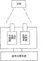
附图1,常规的可见光/红外双光谱探测器系统结构图;Accompanying
附图2,本发明的单片式可见光/红外光双光谱焦平面探测器结构示意图;Accompanying
附图3,本发明的像元结构示意图;Accompanying
附图4,本发明的可见光像元剖面结构示意图;Accompanying
附图5,本发明的红外感光像元剖面结构示意图;Accompanying drawing 5, the schematic diagram of the cross-sectional structure of the infrared photosensitive pixel of the present invention;
附图中:可见光像元1、可见光像元收集二极管2、红外感光像元3、红外感光像元收集二极管4、四相CCD转移栅5、沟阻6、N型保护环7、P型势垒8、P型硅衬底9、二氧化硅层10、V-CCD信道11。In the drawings:
具体实施方式Detailed ways
参见附图1,常规的可见光/红外双光谱探测器系统结构图,可见光探测系统和红外探测系统同时对目标进行成像,在相应的探测系统中可以观测到相应可见光或红外的像;而后端的信号处理系统则可以对前端探测到的可见光和红外信号进行融合处理,得到双波段信号融合的图像;这种成像方式的缺点在于两幅图像不可能完全重合,这就会影响到信号融合后的图像的清晰度。Referring to Figure 1, the structural diagram of a conventional visible light/infrared dual-spectrum detector system, the visible light detection system and the infrared detection system simultaneously image the target, and the corresponding visible light or infrared image can be observed in the corresponding detection system; while the signal at the back end The processing system can fuse the visible light and infrared signals detected by the front end to obtain a dual-band signal fusion image; the disadvantage of this imaging method is that the two images cannot be completely overlapped, which will affect the image after signal fusion clarity.
参见附图3,本发明的像元结构示意图,由于本发明的单片式可见光/红外光双光谱焦平面探测器,针对两个不同的波段分别设计有可见光像元1和红外感光像元3,因此利用该结构不仅可以在单芯片上实现双光谱的探测,而且有利于对双波段的信号实现实时的融合和分离处理,提高探测器对目标的识别能力;同时其制作工艺与现有的可见光/红外双光谱探测器制作工艺完全兼容,便于制作生产。Referring to accompanying drawing 3, the schematic diagram of the pixel structure of the present invention, due to the single-chip visible light/infrared light dual-spectrum focal plane detector of the present invention, a visible
附图3中,可见光像元1和红外感光像元3并列在四相CCD转移栅5的一侧,且可见光像元1和红外感光像元3的位置可互换;可见光像元1和红外感光像元3分别通过可见光像元收集二极管2和红外感光像元收集二极管4把可见光信号和红外信号输入四相CCD转移栅5上的相应电极;各个器件间用沟阻6隔离,防止信号间的相互干扰。In accompanying drawing 3, the visible
参见附图3,通常情况下红外响应要明显比可见光响应低,因此在设计时增大了红外感光像元3的感光面积以提高其响应,红外感光像元3的尺寸为30(H)×40(V)μm2,可见光像元1的尺寸为30(H)×20(V)μm2(上述尺寸为任意选取的一种);由四相CCD转移栅5上的电极V1、V2、V3、V4构成的CCD信道宽为7μm;为了降低PtSi红外探测器(由红外感光像元3和其它相关结构组成)热噪声和暗电流,PtSi二极管(红外感光像元3)周围设计了N型保护环;光信号从正面入射,在PtSi膜内产生电子空穴对,能量高于PtSi肖特基势垒的热空穴注入衬底,留在PtSi膜内的电子即为信号电荷;可见光像元1则设计成光敏二极管。Referring to accompanying drawing 3, usually the infrared response is significantly lower than the visible light response, so the photosensitive area of the infrared
参见附图2,本发明的单片式可见光/红外光双光谱焦平面探测器结构示意图(图中箭头所指方向为信号传输方向),本发明的单片式可见光/红外光双光谱焦平面探测器,采用内线转移结构,信号电荷通过四相结构的垂直埋沟CCD移位寄存器(四相CCD转移栅5)转移到四相的水平埋沟CCD移位寄存器(四相CCD转移栅5),最后由输出放大器输出;当探测器工作时,偶数行对红外响应,奇数行对可见光响应,利用CCD隔行扫描模式,可在偶场读出红外图像,奇场读出可见光图像的方案。Referring to accompanying drawing 2, the single-chip visible light/infrared light dual-spectrum focal plane detector structure schematic diagram of the present invention (the direction indicated by the arrow in the figure is the signal transmission direction), the single-chip visible light/infrared light dual-spectrum focal plane of the present invention The detector adopts an internal line transfer structure, and the signal charge is transferred to the four-phase horizontal buried trench CCD shift register (four-phase CCD transfer gate 5) through the four-phase vertical buried trench CCD shift register (four-phase CCD transfer gate 5) , and finally output by the output amplifier; when the detector is working, the even lines respond to infrared, and the odd lines respond to visible light. Using the CCD interlaced scanning mode, the infrared image can be read out in the even field, and the visible light image can be read out in the odd field.
参见附图4、附图5,图中箭头所指方向为光入射方向,衬底采用P型硅衬底9,对于红外感光像元3在其表面制备出厚度不大于5nm的PtSi薄膜(图中略)。为了降低PtSi探测器热噪声和暗电流,PtSi二极管周围设计有N型保护环7。对于可见光像元1则在P型硅衬底9上注入一层N型掺杂层形成光敏二极管。光信号从PtSi或光敏二极管正面入射,在PtSi薄膜或光敏二极管内产生信号电荷。P型势垒8则控制信号电荷的转出。除感光的区域外,器件其余地方用厚的二氧化硅层10覆盖。Referring to accompanying drawing 4, accompanying drawing 5, the direction indicated by arrow among the figure is light incident direction, and substrate adopts P-
实施例1:Example 1:
参见附图3,一种单片式可见光/红外光双光谱焦平面探测器,它包括:可见光像元1、可见光像元收集二极管2、红外感光像元3、红外感光像元收集二极管4、四相CCD转移栅5上的电极V1、V2、V3、V4,各个电极按上述顺序从上至下排列并构成CCD信道;可见光像元1和红外感光像元3并列在四相CCD转移栅5的一侧,且可见光像元1和红外感光像元3的位置可互换;可见光像元1和红外感光像元3分别通过可见光像元收集二极管2和红外感光像元收集二极管4把可见光信号和红外信号输入四相CCD转移栅5上的相应电极;各个器件间用沟阻6隔离,防止信号间的相互干扰。Referring to accompanying drawing 3, a kind of monolithic visible light/infrared light dual-spectrum focal plane detector, it comprises: visible
由于器件采用三电平工作方式输出信号,光敏二极管(可见光像元1)和PtSi二极管(红外感光像元3)与V-CCD信道11对应电极分别为V1和V3(即可见光像元收集二极管2把可见光信号输出到电极V1,红外感光像元收集二极管4把红外信号输出到电极V3),使得器件可采用场积分和帧积分两种模式进行工作。Since the device uses a three-level working mode to output signals, the corresponding electrodes of the photosensitive diode (visible light pixel 1) and PtSi diode (infrared photosensitive pixel 3) and V-
其工作方式如下:It works like this:
场积分模式下:电极V1和V3同时加高电平,奇数行的光敏二极管中积累的可见光信号和偶数行的PtSi二极管中积累的红外信号同时转出后,奇场时,信号电荷通过电极V2下面的CCD进行叠加然后依次转移,偶场时,信号电荷通过电极V4下面的CCD进行叠加然后依次转移,完成一场信号的输出。In the field integration mode: the electrodes V1 and V3 are high at the same time, after the visible light signals accumulated in the photodiodes of the odd rows and the infrared signals accumulated in the PtSi diodes of the even rows are transferred out at the same time, in the odd field, the signal charge passes through the electrode V2 The lower CCDs are superimposed and then transferred sequentially. In an even field, the signal charges are superimposed and transferred sequentially through the CCD below the electrode V4 to complete the output of one field signal.
帧积分模式下:在奇场信号转出时,对应的电极V1为高电平,奇数行的PtSi二极管积累的电荷通过表沟势垒区转移进入相应的电极V1,然后依次转移,此时偶数行PtSi二极管对光信号进行积分。在偶场信号转出时,对应电极V3,偶数行的PtSi二极管积累的电荷被读出,然后依次转移,同时奇数行PtSi二极管对光信号进行积分,依次重复进行,完成一帧信号输出。In the frame integration mode: when the odd field signal is transferred out, the corresponding electrode V1 is at a high level, and the charges accumulated by the PtSi diodes in the odd rows are transferred into the corresponding electrode V1 through the surface trench potential barrier region, and then transferred in turn. At this time, the even Rows of PtSi diodes integrate the light signal. When the even field signal is transferred out, corresponding to the electrode V3, the charges accumulated by the PtSi diodes in the even rows are read out, and then transferred sequentially. At the same time, the PtSi diodes in the odd rows integrate the optical signal, and the process is repeated in sequence to complete a frame of signal output.
依据器件的工作模式,完成图像的融合与隔离成像可以有两种方法:According to the working mode of the device, there are two ways to complete image fusion and isolation imaging:
1)单独从驱动电路上着手进行控制,让器件工作在场积分模式,通过跳线或者开关控制FPGA(现场可编程逻辑阵列)的引脚输入来控制驱动时序脉冲的发生。融合成像时,控制时序发生电路按正常场积分模式工作,使得信号电荷在CCD器件读出转移的过程中便得到融合;单光谱成像时,如单独成可见光像,控制时序发生电路,将电极V3的三电平关掉,只读出电极V1下面的信号电荷,即可见光响应的信号,依次转移读出,单独成红外像时,类似的关掉电极V1的三电平,只读出电极V3下面的信号电荷,即红外响应的信号,依次转移读出,实现单光谱成像。1) Start the control from the driving circuit alone, let the device work in the field integration mode, and control the pin input of the FPGA (Field Programmable Logic Array) through jumpers or switches to control the generation of driving timing pulses. In fusion imaging, the control timing generation circuit works in the normal field integration mode, so that the signal charge is fused during the readout and transfer of the CCD device; in single-spectrum imaging, if a visible light image is formed alone, the timing generation circuit is controlled, and the electrode V3 Turn off the three levels of the electrode V1, and only read the signal charge under the electrode V1, that is, the visible light response signal, which is transferred and read in turn. When the infrared image is formed separately, similarly turn off the three levels of the electrode V1, and only read the electrode V3 The underlying signal charge, that is, the signal of the infrared response, is sequentially transferred for readout, enabling single-spectrum imaging.
2)从图像处理的角度着手,让器件工作在隔行扫描的帧积分模式下,先将依次转移读出的模拟信号转换成数字信号,用FPGA做控制及接口器件,将数字信号分场存储于存储芯片中,通过串口(UTAR)接收命令控制图像的处理与显示。单光谱成像时,通过FPGA控制从存储芯片实时取出奇场信号(偶场)传送到DA(数模转换),并在接下来的偶场(奇场)时间内将该场的信号重复读出一次以满足PAL制式,实现单光谱成像;多光谱融合成像时,则要读出存储器中两场的数字信号,在FPGA内通过一定的算法将数字信息处理后再送出到DA转换成电视信号,完成多光谱融合成像。2) From the perspective of image processing, let the device work in the frame integration mode of interlaced scanning, first convert the analog signals read out in sequence into digital signals, use FPGA as the control and interface device, and store the digital signals in separate fields In the memory chip, commands are received through the serial port (UTAR) to control image processing and display. During single-spectrum imaging, the odd field signal (even field) is taken out from the memory chip in real time through FPGA control and sent to DA (digital-to-analog conversion), and the signal of the field is repeatedly read out in the next even field (odd field) time Once to meet the PAL standard, realize single-spectrum imaging; when multi-spectral fusion imaging, it is necessary to read out the digital signals of two fields in the memory, process the digital information through a certain algorithm in the FPGA, and then send it to the DA to convert it into a TV signal. Completion of multi-spectral fusion imaging.
实施例2:Example 2:
实施例2与实施例1的不同之处在于:可见光像元1和红外感光像元3的位置进行了互换,并且红外感光像元收集二极管4把红外信号输出到电极V1,可见光像元收集二极管2把可见光信号输出到电极V3,其余结构也作相应改变;进行这种改变后,其工作原理和过程与实施例1相类似。The difference between
Claims (8)
Priority Applications (1)
| Application Number | Priority Date | Filing Date | Title |
|---|---|---|---|
| CN2008100693419ACN101231193B (en) | 2008-02-01 | 2008-02-01 | Monolithic Visible/Infrared Dual Spectrum Focal Plane Detector |
Applications Claiming Priority (1)
| Application Number | Priority Date | Filing Date | Title |
|---|---|---|---|
| CN2008100693419ACN101231193B (en) | 2008-02-01 | 2008-02-01 | Monolithic Visible/Infrared Dual Spectrum Focal Plane Detector |
Publications (2)
| Publication Number | Publication Date |
|---|---|
| CN101231193A CN101231193A (en) | 2008-07-30 |
| CN101231193Btrue CN101231193B (en) | 2010-06-09 |
Family
ID=39897845
Family Applications (1)
| Application Number | Title | Priority Date | Filing Date |
|---|---|---|---|
| CN2008100693419AExpired - Fee RelatedCN101231193B (en) | 2008-02-01 | 2008-02-01 | Monolithic Visible/Infrared Dual Spectrum Focal Plane Detector |
Country Status (1)
| Country | Link |
|---|---|
| CN (1) | CN101231193B (en) |
Families Citing this family (5)
| Publication number | Priority date | Publication date | Assignee | Title |
|---|---|---|---|---|
| CN104266761B (en)* | 2014-10-13 | 2017-02-15 | 中国电子科技集团公司第四十四研究所 | Method for restraining background currents of focal plane detector |
| CN107346774A (en)* | 2016-05-05 | 2017-11-14 | 上海芯晨科技有限公司 | A kind of single chip integrated ultraviolet FPA and preparation method thereof |
| CN106595870B (en)* | 2016-12-08 | 2019-12-31 | 苏州长风航空电子有限公司 | Infrared imaging device and heterogeneity processing method thereof |
| CN111430397B (en)* | 2020-04-01 | 2022-08-02 | 中国电子科技集团公司第四十四研究所 | Multi-spectrum TDICCD structure with antireflection film |
| CN112577612B (en)* | 2020-12-09 | 2022-04-08 | 中国电子科技集团公司第四十四研究所 | Black silicon plasmon auxiliary absorption thermopile chip and manufacturing method thereof |
Citations (2)
| Publication number | Priority date | Publication date | Assignee | Title |
|---|---|---|---|---|
| EP1503580A1 (en)* | 2003-07-30 | 2005-02-02 | DaimlerChrysler AG | Sensor arrangement including a plurality of sensor types |
| CN1723564A (en)* | 2003-11-10 | 2006-01-18 | 松下电器产业株式会社 | Imaging device and imaging method |
- 2008
- 2008-02-01CNCN2008100693419Apatent/CN101231193B/ennot_activeExpired - Fee Related
Patent Citations (2)
| Publication number | Priority date | Publication date | Assignee | Title |
|---|---|---|---|---|
| EP1503580A1 (en)* | 2003-07-30 | 2005-02-02 | DaimlerChrysler AG | Sensor arrangement including a plurality of sensor types |
| CN1723564A (en)* | 2003-11-10 | 2006-01-18 | 松下电器产业株式会社 | Imaging device and imaging method |
Also Published As
| Publication number | Publication date |
|---|---|
| CN101231193A (en) | 2008-07-30 |
Similar Documents
| Publication | Publication Date | Title |
|---|---|---|
| TWI406402B (en) | Circuitry for backside illuminated image sensor overlaps with light sensor | |
| CN106847841B (en) | Solid-state imaging devices and electronic equipment | |
| US10270996B2 (en) | Image sensor including a pixel unit having an autofocusing pixel and a normal pixel and driving method thereof | |
| TWI407555B (en) | Back side light receiving image sensor and control method thereof | |
| KR102730554B1 (en) | Solid-state imaging element, production method and electronic device | |
| US9880057B2 (en) | Visible and near-infrared radiation detector | |
| CN101939982B (en) | Backside illuminated image sensor with global shutter and storage capacitor | |
| JP4500574B2 (en) | Wide dynamic range color solid-state imaging device and digital camera equipped with the solid-state imaging device | |
| CN101465364B (en) | Solid-state imaging device and camera | |
| US9040916B2 (en) | Visible and near-infrared radiation detector | |
| TWI360223B (en) | Image sensor with high fill factor pixels and meth | |
| US20130026548A1 (en) | Image sensor with controllable vertically integrated photodetectors | |
| US8339494B1 (en) | Image sensor with controllable vertically integrated photodetectors | |
| JPWO2014097899A1 (en) | Solid-state imaging device | |
| TW201523849A (en) | Solid-state image sensing device | |
| CN106488148B (en) | A kind of super-resolution image sensor and its building method | |
| US8730362B2 (en) | Image sensor with controllable vertically integrated photodetectors | |
| CN101231193B (en) | Monolithic Visible/Infrared Dual Spectrum Focal Plane Detector | |
| US20130026594A1 (en) | Image sensor with controllable vertically integrated photodetectors | |
| WO2016104177A1 (en) | Solid-state image capture element, method for manufacturing same, and electronic component | |
| CN103531601B (en) | A kind of large area cmos image sensor for direct detection X ray | |
| US8946612B2 (en) | Image sensor with controllable vertically integrated photodetectors | |
| US8736728B2 (en) | Image sensor with controllable vertically integrated photodetectors | |
| CN104092963A (en) | Reconfigurable CMOS image sensor chip |
Legal Events
| Date | Code | Title | Description |
|---|---|---|---|
| C06 | Publication | ||
| PB01 | Publication | ||
| C10 | Entry into substantive examination | ||
| SE01 | Entry into force of request for substantive examination | ||
| C14 | Grant of patent or utility model | ||
| GR01 | Patent grant | ||
| C17 | Cessation of patent right | ||
| CF01 | Termination of patent right due to non-payment of annual fee | Granted publication date:20100609 Termination date:20140201 |