CN101226449A - Capacitive Sensing and Absolute Position Mapping in Displacement-Type Pointing Devices - Google Patents
Capacitive Sensing and Absolute Position Mapping in Displacement-Type Pointing DevicesDownload PDFInfo
- Publication number
- CN101226449A CN101226449ACNA2008100000650ACN200810000065ACN101226449ACN 101226449 ACN101226449 ACN 101226449ACN A2008100000650 ACNA2008100000650 ACN A2008100000650ACN 200810000065 ACN200810000065 ACN 200810000065ACN 101226449 ACN101226449 ACN 101226449A
- Authority
- CN
- China
- Prior art keywords
- sensing
- electrodes
- coupling element
- electrode
- conductive coupling
- Prior art date
- Legal status (The legal status is an assumption and is not a legal conclusion. Google has not performed a legal analysis and makes no representation as to the accuracy of the status listed.)
- Granted
Links
Images


Classifications
- G—PHYSICS
- G06—COMPUTING OR CALCULATING; COUNTING
- G06F—ELECTRIC DIGITAL DATA PROCESSING
- G06F3/00—Input arrangements for transferring data to be processed into a form capable of being handled by the computer; Output arrangements for transferring data from processing unit to output unit, e.g. interface arrangements
- G06F3/01—Input arrangements or combined input and output arrangements for interaction between user and computer
- G06F3/03—Arrangements for converting the position or the displacement of a member into a coded form
- G06F3/033—Pointing devices displaced or positioned by the user, e.g. mice, trackballs, pens or joysticks; Accessories therefor
- G06F3/0354—Pointing devices displaced or positioned by the user, e.g. mice, trackballs, pens or joysticks; Accessories therefor with detection of 2D relative movements between the device, or an operating part thereof, and a plane or surface, e.g. 2D mice, trackballs, pens or pucks
- G06F3/03543—Mice or pucks
- G—PHYSICS
- G06—COMPUTING OR CALCULATING; COUNTING
- G06F—ELECTRIC DIGITAL DATA PROCESSING
- G06F3/00—Input arrangements for transferring data to be processed into a form capable of being handled by the computer; Output arrangements for transferring data from processing unit to output unit, e.g. interface arrangements
- G06F3/01—Input arrangements or combined input and output arrangements for interaction between user and computer
- G06F3/03—Arrangements for converting the position or the displacement of a member into a coded form
- G06F3/041—Digitisers, e.g. for touch screens or touch pads, characterised by the transducing means
- G06F3/044—Digitisers, e.g. for touch screens or touch pads, characterised by the transducing means by capacitive means
- G06F3/0447—Position sensing using the local deformation of sensor cells
- G—PHYSICS
- G06—COMPUTING OR CALCULATING; COUNTING
- G06F—ELECTRIC DIGITAL DATA PROCESSING
- G06F2203/00—Indexing scheme relating to G06F3/00 - G06F3/048
- G06F2203/041—Indexing scheme relating to G06F3/041 - G06F3/045
- G06F2203/04107—Shielding in digitiser, i.e. guard or shielding arrangements, mostly for capacitive touchscreens, e.g. driven shields, driven grounds
Landscapes
- Engineering & Computer Science (AREA)
- General Engineering & Computer Science (AREA)
- Theoretical Computer Science (AREA)
- Human Computer Interaction (AREA)
- Physics & Mathematics (AREA)
- General Physics & Mathematics (AREA)
- Position Input By Displaying (AREA)
Abstract
Translated fromChinese
Description
Translated fromChinese技术领域technical field
本发明涉及位移型定点设备(displacement type pointing device)中的电容传感(capacitive sensing)和绝对位置映射。The present invention relates to capacitive sensing and absolute position mapping in displacement type pointing devices.
背景技术Background technique
已经开发出许多种定点设备,用于向机器输入命令。例如,诸如计算机鼠标、操纵杆(joystick)、跟踪球(trackball)、触摸屏和键盘之类的手控定点设备共同地被用于通过操作定点设备来向计算机输入指令。这种定点设备允许用户控制光标(即,虚拟指针)在计算机屏幕上的移动、选择或移动显示在计算机屏幕上的图标或其它虚拟物体、以及打开和关闭与不同输入命令相对应的菜单项目。Many types of pointing devices have been developed for entering commands to machines. For example, hand-controlled pointing devices such as computer mice, joysticks, trackballs, touch screens, and keyboards are commonly used to input instructions to computers by operating the pointing devices. Such pointing devices allow a user to control the movement of a cursor (ie, a virtual pointer) on a computer screen, select or move icons or other virtual objects displayed on the computer screen, and open and close menu items corresponding to various input commands.
已经开发出用于趋向于保持固定的、诸如台式计算机之类的大型电子设备的定点设备,以及用于诸如蜂窝电话和移动计算机系统之类的小型便携式电子设备的定点设备。与用于便携式电子设备的定点设备相比,一般地,用于大型电子设备的定点设备具有更少和更灵活的设计限制,原因在于其可以使用更大的空间和更多的功率资源。一般而言,用于便携式电子设备的定点设备应当允许用户快速精确地移动光标,并且在有限的工作空间和功率限制内进行操作。Pointing devices have been developed for large electronic devices, such as desktop computers, which tend to remain stationary, and for small portable electronic devices, such as cellular telephones and mobile computer systems. Pointing devices for large electronic devices generally have fewer and more flexible design constraints than pointing devices for portable electronic devices because they can use more space and power resources. In general, pointing devices for portable electronic devices should allow a user to move a cursor quickly and precisely, and operate within limited workspace and power constraints.
已经开发出位移型定点设备,用以满足便携式电子设备的固有限制。这些类型的定点设备包括可位移构件(例如,手持游标器(puck)、按钮或者其它可移动物体),该可位移构件在例如通过用户的手指来施加压力之后在限定的运动场内移动。在典型的位移型定点设备中,可位移构件响应于平面方向上的横向力而进行二维移动。电阻器电路、电容传感器和磁性(霍尔效应,Hall-effect)传感器已经被用于确定可位移构件在运动场中的位移。所确定的可位移构件的位移被映射成显示器上的光标的二维移动。在用户释放可移动构件之后,一般地,恢复机构(例如,一组弹簧)将可位移构件返回到运动场中的中心位置。当可移动构件位于运动场的中心位置时,位置映射系统一般地固定显示器上的光标位置。Displacement-type pointing devices have been developed to meet the inherent limitations of portable electronic devices. These types of pointing devices include a displaceable member (eg, a hand-held puck, button, or other movable object) that moves within a defined field of play upon application of pressure, eg, by a user's finger. In a typical displacement-type pointing device, a displaceable member moves two-dimensionally in response to a lateral force in a planar direction. Resistor circuits, capacitive sensors and magnetic (Hall-effect) sensors have been used to determine the displacement of the displaceable member in the motion field. The determined displacement of the displaceable member is mapped to two-dimensional movement of a cursor on the display. After the user releases the movable member, typically a return mechanism (eg, a set of springs) returns the displaceable member to a central position in the playing field. The position mapping system generally fixes the position of the cursor on the display when the movable member is located in the center of the playing field.
可位移构件的运动场一般地非常小。其结果是,位移型定点设备一般地以相对设备-光标映射模式或速度映射(或,操纵杆)模式来进行操作。在相对设备-光标映射模式下,可位移构件的位置和显示器上的光标的位置可以利用可变映射来平衡。在速度映射模式下,可位移构件的位置被映射成显示器上的光标的速度。一般地,可位移构件的运动场太小以至于无法提供绝对的设备-光标映射模式,在绝对的设备-光标映射模式下,可位移构件的位置和屏幕上的光标的位置一一对应。The field of play of the displaceable member is generally very small. As a result, displacement-type pointing devices generally operate in either a relative device-to-cursor mapping mode or a velocity mapping (or, joystick) mode. In the relative device-to-cursor mapping mode, the position of the displaceable member and the position of the cursor on the display can be balanced using a variable mapping. In velocity mapping mode, the position of the displaceable member is mapped to the velocity of a cursor on the display. Typically, the motion field of the displaceable member is too small to provide an absolute device-to-cursor mapping mode in which the position of the displaceable member corresponds to the position of the cursor on the screen.
需要的是这样的位移型定点设备和方法,该设备和方法能够高精确度地感应可位移构件的移动,并提供输入的绝对位置映射模式,其中可位移构件的位置和显示器上的光标的位置一一对应的。What is needed is a displacement-type pointing device and method that senses the movement of a displaceable member with high accuracy and provides an absolute position mapping mode of input wherein the position of the displaceable member and the position of a cursor on a display corresponding.
发明内容Contents of the invention
在一个方面,本发明的特征在于一种输入装置,该输入装置包括传感系统、可位移构件、测量系统和处理系统。传感系统包括传感电极和至少一个驱动电极的空间排列阵。可位移构件在传感系统上的操作区域中移动,并且包括电导耦合元件,该电导耦合元件可用于将来自所述至少一个驱动电极的信号电容耦合至在该电导耦合元件下面的那些传感电极。测量系统生成指示电导耦合元件和那些传感电极之间的重叠量的测量信号。处理系统根据该测量信号来产生具有下述信息的输出信号,所述信息传达与所述电导耦合元件在操作区域中的绝对位置相对应的运动度量。In one aspect, the invention features an input device that includes a sensing system, a displaceable member, a measurement system, and a processing system. The sensing system includes a spatially arrayed array of sense electrodes and at least one drive electrode. The displaceable member moves in an operating region on the sensing system and includes a conductive coupling element operable to capacitively couple signals from the at least one drive electrode to those sensing electrodes underlying the conductive coupling element. The measurement system generates a measurement signal indicative of the amount of overlap between the conductive coupling element and those sensing electrodes. A processing system generates an output signal having information conveying a measure of motion corresponding to an absolute position of the conductive coupling element in the region of operation from the measurement signal.
在其它方面,本发明的特征在于一种输入装置,该输入装置包括传感系统和可位移构件。传感系统包括在操作区域的各个分区中的分区传感电极和至少一个驱动电极的空间排列阵。至少一个所述分区传感电极包括分布在操作区域的各个分区中的电导传感元件。驱动电极包括散布于所述至少一个分区传感电极的传感元件中的分立电导传感元件。可位移构件在传感系统上的操作区域中移动,并且包括电导耦合元件,该电导耦合元件将来自所述至少一个驱动电极的信号电容耦合至在该电导耦合元件下面的那些传感电极。In other aspects, the invention features an input device that includes a sensing system and a displaceable member. The sensing system includes a spatial array of zoned sense electrodes and at least one drive electrode in each zone of the operating area. At least one of said zoned sensing electrodes comprises conductance sensing elements distributed in respective zones of the operating area. The drive electrodes include discrete conductance sensing elements interspersed among the sensing elements of the at least one zoned sensing electrode. A displaceable member moves in an operating region on the sensing system and includes a conductive coupling element that capacitively couples signals from the at least one drive electrode to those sensing electrodes underlying the conductive coupling element.
在另一个方面,本发明的特征在于一种输入方法,根据该输入方法,响应于可位移构件在传感电极和至少一个驱动电极的空间排列阵上的操作区域中的移动,生成这样的测量信号,该测量信号指示所述可位移构件的电导耦合元件和下面的那些传感电极之间的重叠量。根据所述测量信号来产生具有下述信息的输出信号,所述信息传达与所述电导耦合元件在所述操作区域中的绝对位置相对应的运动度量。In another aspect, the invention features a method of input according to which a measurement is generated in response to movement of a displaceable member in an operating region over a spatial array of sense electrodes and at least one drive electrode A signal indicative of the amount of overlap between the conductive coupling elements of the displaceable member and those underlying sensing electrodes. An output signal having information conveying a measure of motion corresponding to the absolute position of the conductive coupling element in the operating region is generated from the measurement signal.
根据以下描述(包括附图和权利要求),本发明的其它特征和优点将变得清楚。Other features and advantages of the invention will become apparent from the following description, including the drawings and claims.
附图说明Description of drawings
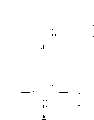
图1是在示例性操作环境中的定点设备的一个实施例的图示,该定点设备包括可位移构件、传感系统、测量系统和处理系统;1 is an illustration of one embodiment of a pointing device including a displaceable member, a sensing system, a measurement system, and a processing system in an exemplary operating environment;
图2A是图1所示的定点设备的一个实施例的示意性顶视图;Figure 2A is a schematic top view of one embodiment of the pointing device shown in Figure 1;
图2B是图2A所示的定点设备沿线2B-2B的截面图;2B is a cross-sectional view of the pointing device shown in FIG. 2A along line 2B-2B;
图3是图1所示的定点设备的一个实施例的截面图;Figure 3 is a cross-sectional view of one embodiment of the pointing device shown in Figure 1;
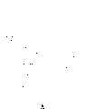
图4A是操作区域的一个实施例的示意性顶视图;Figure 4A is a schematic top view of one embodiment of an operating area;
图4B是传感系统的一个实施例的顶视图,该传感系统包括与图1所示的测量系统的一个实施例相耦合的传感电极和至少一个驱动电极的空间排列阵;Figure 4B is a top view of one embodiment of a sensing system comprising a spatial array of sense electrodes and at least one drive electrode coupled to one embodiment of the measurement system shown in Figure 1;
图5是传感系统的一个实施例的一部分的顶部放大图,该传感系统包括在分区传感电极和驱动电极的相互交错的电极指之间的噪声屏蔽(noise-shielding)电导体;5 is an enlarged top view of a portion of one embodiment of a sensing system that includes noise-shielding electrical conductors between interdigitated electrode fingers of segmented sense electrodes and drive electrodes;
图6是叠加在操作区域的一个实施例上的电导耦合元件的一个实施例的示意性顶视图;Figure 6 is a schematic top view of one embodiment of a conductive coupling element superimposed on one embodiment of an operating region;
图7是叠加在操作区域的一个实施例上的电导耦合元件的一个实施例的示意性顶视图;Figure 7 is a schematic top view of one embodiment of a conductive coupling element superimposed on one embodiment of an operating region;
图8是叠加在传感系统的一个实施例上的、图7所示的操作区域实施例的示意性顶视图;Figure 8 is a schematic top view of the embodiment of the operating area shown in Figure 7 superimposed on an embodiment of the sensing system;
图9A和9B是在图1所示的传感系统实施例上的不同各点处的模拟地示出的电导耦合元件的一个实施例的顶视图;9A and 9B are top views of one embodiment of a conductive coupling element shown analogously at various points on the sensing system embodiment shown in FIG. 1;
图10是在图1所示的传感系统实施例上模拟地示出的电导耦合元件的一个实施例的顶视图;Figure 10 is a top view of one embodiment of a conductive coupling element shown analogously on the sensing system embodiment shown in Figure 1;
图11A是图1的定点设备的一个实施例的示意性截面图,该定点设备包括具有可位移耦合构件的电导耦合元件的一个实施例;11A is a schematic cross-sectional view of one embodiment of the pointing device of FIG. 1 including one embodiment of a conductive coupling element having a displaceable coupling member;
图11B是图11A所示的定点设备的示意性截面图,其中,可位移耦合构件已经响应于用户手指所施加的垂直力而向传感系统移动;11B is a schematic cross-sectional view of the pointing device shown in FIG. 11A, wherein the displaceable coupling member has moved toward the sensing system in response to a vertical force applied by a user's finger;
图12A和12B各自为电导耦合元件的一个实施例的顶视图和仰视图,该电导耦合元件包括环绕中心电导耦合元件的外围电导耦合元件,所述中心电导耦合元件包括可位移耦合构件;12A and 12B are top and bottom views, respectively, of one embodiment of a conductance coupling element comprising peripheral conductance coupling elements surrounding a central conductance coupling element comprising a displaceable coupling member;
图13是图1所示的可位移构件的一个实施例的示意性截面图;Figure 13 is a schematic cross-sectional view of one embodiment of the displaceable member shown in Figure 1;
图14是处理系统的一个实施例和测量电路的一个实施例的框图,该测量电路与图9A和9B所示的电导耦合元件和传感系统的等效电路电连接;Figure 14 is a block diagram of one embodiment of a processing system and one embodiment of a measurement circuit in electrical connection with the equivalent circuit of the conductive coupling element and sensing system shown in Figures 9A and 9B;
图15是图1所示的测量电路的一个实施例的电路图;Figure 15 is a circuit diagram of one embodiment of the measurement circuit shown in Figure 1;
图16是使用图9A和9B所示的传感系统来获得测量值的方法的一个实施例的流程图;Figure 16 is a flowchart of one embodiment of a method of obtaining measurements using the sensing system shown in Figures 9A and 9B;
图17是从根据图16的方法来生成的测量值中产生显示控制信号的方法的一个实施例的流程图;17 is a flowchart of one embodiment of a method of generating display control signals from measurements generated according to the method of FIG. 16;
图18是根据图16的方法、在测量周期中测得的总电容作为时间的函数来绘制的图形;Fig. 18 is a graph plotted as a function of time of total capacitance measured during a measurement cycle according to the method of Fig. 16;
图19是可以由图1所示的定点设备的实施例来执行的方法的一个实施例的流程图;Figure 19 is a flowchart of one embodiment of a method that may be performed by the embodiment of the pointing device shown in Figure 1;
图20A是在图1所示的定点设备的一个实施例中、正从操作区域中的第一位置向第二位置移动的可位移构件的示意性示图;FIG. 20A is a schematic illustration of a displaceable member being moved from a first position to a second position in an operating region in one embodiment of the pointing device shown in FIG. 1;
图20B是根据绝对位置映射输入方法的一个实施例、响应于图20A所示的可位移构件的移动而正从显示屏幕中的第一位置向第二位置移动的光标的示意性示图。Figure 20B is a schematic illustration of a cursor being moved from a first position to a second position in a display screen in response to movement of the displaceable member shown in Figure 20A, according to one embodiment of an absolute position mapping input method.
具体实施方式Detailed ways
在以下的描述中,相似的标号用于标识相似元件。此外,附图意在以图示方式来示出示例性实施例的主要特征。附图并不意在示出实际实施例的每一个特征,也不意在示出所描绘的元件的相对尺度,并且附图的绘制并不成比例。In the following description, like reference numerals are used to identify like elements. Furthermore, the drawings are intended to illustrate key features of the exemplary embodiments by way of illustration. The drawings are not intended to show every feature of actual embodiments nor relative scale of the depicted elements, and the drawings are not drawn to scale.
I.引言I. Introduction
图1示出了定点设备10的一个实施例,定点设备10包括可位移构件12、传感系统14、测量系统16和处理系统18。以下将详细描述,定点设备10能够高精确度地感应可位移构件12的移动,并提供输入的绝对位置映射模式,在该模式中,可位移构件12的位置被一一对应地映射成光标的位置。FIG. 1 illustrates one embodiment of a pointing device 10 that includes a displaceable member 12 , a
一般而言,定点设备10可以并入到输入控制信号起到有用的目的任何类型的设备或系统中。为了说明的目的,定点设备10在这里被描述成用于将图形用户界面命令输入到机器(例如,便携式或台式计算机)中的系统组件。在图1所示的示意性操作环境中,定点设备10将输出信号20发送到对显示器24进行驱动的显示控制器22。在一些实施例中,处理系统18产生具有传达运动度量的信息的输出信号20,所述运动度量指示可位移构件12在操作区域中的移动。处理系统18可以产生的输出信号20的示例类型包括:描述了可位移构件12的绝对或相对位置的位置数据(例如,以操作区域的指定原点为中心的坐标系统的轴向距离);描述了可位移构件12的速度的速度数据;以及滚动位置和距离数据。显示控制器22对输出信号20进行处理,以例如控制显示器24上的光标25的移动。In general, pointing device 10 may be incorporated into any type of device or system in which input control signals serve a useful purpose. For purposes of illustration, pointing device 10 is described herein as a system component for entering graphical user interface commands into a machine (eg, a portable or desktop computer). In the exemplary operating environment shown in FIG. 1 , pointing device 10 sends output signals 20 to display controller 22 , which drives
在一些实施例中,定点设备10和显示器24被集成为一个整体设备,例如便携式(例如,手持式)电子设备。便携式电子设备可以是人们能够容易地携带的任何类型的设备,包括蜂窝电话、无绳电话、传呼机、个人数字助理(PDA)、数字音频播放器、数码相机和数字视频游戏机。在其它实施例中,定点设备10和显示器24被实现为分离的独立设备,例如,分离的定点设备和基于远程显示器的系统。一般而言,远程系统可以是接收用户输入的、任何类型的基于显示器的电器,包括通用计算机系统、专用计算机系统和视频游戏系统。显示控制信号20可以经有线通信链路(例如,诸如RS-232串行端口、通用串行总线或PS/2端口之类的串行通信链路)或无线通信链路(例如,红外(IR)无线链路或射频(RF)无线链路)被发送到远程系统。在这些实施例中的一些中,可以将一个或多个模块并入(因而可以将处理系统18的一个或多个功能并入)远程系统,而不是并入定点设备10。In some embodiments, pointing device 10 and
处理系统18一般地通过一个或多个分立模块来实现,该分立模块并不限于任何特定的硬件、固件或软件配置。所述一个或多个模块可以在任何计算或数据处理环境中实现,包括在数字电子电路中(例如,诸如数字信号处理器(DSP)之类的专用集成电路)或者在计算机硬件、固件、设备驱动器或软件中。在一些实施例中,用于实现处理系统18的模块的计算机处理指令和由这些模块生成的数据被存储在一个或多个计算机可读介电中。适于有形地收录这些指令和数据的存储设备包括所有形式的非易失存储器,例如包括:诸如EPROM、EEPROM和闪存设备之类的半导体存储设备,诸如内部硬盘和可移动磁盘之类的磁盘,磁光盘,以及CD/DVD-ROM。
显示控制器22一般地运行驱动器以对输出信号20进行处理。一般而言,驱动器可以在任何计算或处理环境中实现,包括在数字电子电路中、或者在计算机硬件、固件或软件中。在一些实施例中,驱动器是操作系统或应用程序的组件。Display controller 22 generally operates drivers to process
显示器24例如可以是平板显示器,例如,LCD(液晶显示器)、等离子体显示器、EL显示器(电致发光显示器)和FED(场发射显示器)。The
以下将详细描述,可位移构件12包括电导耦合元件,而传感系统14包括传感电极和至少一个驱动电极的空间排列阵。可位移构件12可以用手持游标器、按钮或其它可移动物体来实现。在一些实施例中,可位移构件12由电导体组成,在这种情况下,可位移构件12完全由电导耦合元件组成。在其它实施例中,除了电导耦合元件之外,可位移构件12还包括其它元件(例如,输入按钮)。As will be described in detail below, the displaceable member 12 includes a conductive coupling element, and the
可位移构件12可以在受限的运动区域中移动,该受限运动区域在这里称为“操作区域”(operational zone)。在一种示例性操作模式下,用户的手指26在操作区域内操纵可位移构件12,并且传感系统14检测可位移构件在操作区域中的位置。电导耦合元件将测量系统16施加给所述至少一个驱动电极的输入信号28电容性耦合至在电导耦合元件下面的那些传感电极。响应于所施加的输入信号28,传感电极产生传感信号30,该传感信号30是对用户手指26对可位移构件12的触摸的响应,并且是对可位移构件12在操作区域中的不同位置的响应。The displaceable member 12 is movable within a restricted motion zone, referred to herein as an "operational zone". In one exemplary mode of operation, a user's
II.传感系统和可位移构件的示例性实施例II. Exemplary Embodiments of Sensing Systems and Displaceable Members
图2A示出了定点设备10的示例性实施例40的顶视图。图2B示出了定点设备40沿线2B-2B的截面图。在定点设备40中,可位移构件12用手持游标器42来实现。手持游标器42可以在由支撑框架46的围壁45限定的操作区域44中移动。操作区域44可以具有任何形状,包括弯曲形状(例如,椭圆形和圆形)、多边形状(例如,矩形)和曲线形状。在图示的实施例中,操作区域44具有圆角矩形的形状,该圆角的曲率半径与圆形手持游标器42的半径相匹配。支撑框架46安装在基板48(例如,印制电路板)上。传感系统14设在手持游标器42之下、基板48之上。FIG. 2A shows a top view of an exemplary embodiment 40 of pointing device 10 . FIG. 2B shows a cross-sectional view of pointing device 40 along line 2B-2B. In pointing device 40 , displaceable member 12 is implemented with a hand-held
在操作时,手持游标器42响应于用户手指26所施加的横向力(即,具有图2A所示的x-y平面中的分量的力)而在操作区域44内自由移动。手持游标器42可以在传感系统14之上、在支撑面50上滑动,支撑面50可以是传感系统14的低摩擦的电绝缘顶层。在一些实施例中,手持游标器42被限制于在操作区域44内进行二维移动。In operation, hand-held
在一些实施例中,磁性机构将手持游标器42限制于在支撑面50上进行二维移动。例如,在一些示例性实施例中,手持游标器42被磁性吸引至支撑结构50。在这些实施例中,手持游标器42和支撑结构50中的一个或这两者都可以各自包括永磁体。In some embodiments, a magnetic mechanism constrains hand-held
在其它实施例中,机械机构将手持游标器42限制于在支撑面50上进行二维移动。例如,图3示出了图2B所示的定点设备40的一个实施例52,其中,可位移构件包括把手56和基座58,并且支撑框架46用壳体60来实现,壳体60包括顶部62和侧壁64。顶部62包括侧壁66,侧壁66限定了开口68,把手56通过该开口68来伸出。可位移构件54的操作区域一般地由把手56在开口68内的运动范围来限定。可位移构件54的基座58在空腔70内自由地横向滑动,空腔70形成在壳体60的侧壁64和顶部62之间。这样,壳体60将可位移构件54限制于在支撑面50上进行二维移动。In other embodiments, a mechanical mechanism constrains hand-held
在一些实施例中,传感系统14包括在操作区域的各个分区中的分区(regional)传感电极和至少一个驱动电极。在这些实施例的一些中,至少一个所述分区传感电极包括分布在操作区域的各个分区中的分立电导传感元件,而驱动电极包括散布于所述至少一个分区传感电极的传感元件中的分立电导传感元件。In some embodiments,
图4A和4B示出了操作区域94的一个实施例以及传感系统14的一个实施例72,该传感系统14包括四个分区传感电极74、76、78、80和一个驱动电极82。驱动电极82包括一种式样(pattern)的电极指84,而各个分区传感电极74-80包括各自式样的电极指86、88、90、92。驱动电极82的电极指84分布在操作区域94中,该操作区域94经图4B中的电极指84-92的式样来模拟示出。分区传感电极74-80的电极指86-92位于操作区域94的各个分区中。具体而言,分区传感电极74的电极指86位于分区1中,分区传感电极76的电极指88位于分区2中,分区传感电极78的电极指90位于分区3中,而分区传感电极80的电极指92位于分区4中。4A and 4B illustrate one embodiment of an
分区传感电极74-80的电极指86-92一般地排列成规则阵列,该规则阵列提供了跨操作区域94的各个分区的均一密度的电极指。在传感系统72中,驱动电极82的电极指84散布于分区传感电极74-80的电极指86-92中。具体而言,分区传感电极74-80的电极指86-92与驱动电极82的电极指84相互交叉从而形成交错的电极指阵列,在该电极指阵列中,驱动电极82的电极指84穿插在操作区域94的各个分区中的分区传感电极74-80的电极指86-92之间。The electrode fingers 86 - 92 of the zoned sense electrodes 74 - 80 are generally arranged in a regular array that provides a uniform density of electrode fingers across the various zones of the operating
在图示的实施例中,传感电极74-82被排列在基板48(参见图2B)的平面上。在其它实施例中,传感电极74-82被排列在基板48的一个或多个弯曲(例如,凸起或凹陷)表面上。In the illustrated embodiment, the sense electrodes 74-82 are arranged in the plane of the substrate 48 (see FIG. 2B). In other embodiments, sense electrodes 74 - 82 are arranged on one or more curved (eg, convex or concave) surfaces of
图5示出了传感系统72的一个实施例96的一部分,该传感系统72额外包括至少一个噪声屏蔽电导体,该噪声屏蔽电导体介于分区传感电极74-80的电极指86-92与相邻的、驱动电极82的电极指84之间。在图5所示的传感系统96的所述部分中,噪声屏蔽电导体98穿插在驱动电极82的电极指84与分区传感电极76的电极指88之间。噪声屏蔽电导体98与参考电位100电气连接,该参考电位100一般地是地电位。噪声屏蔽电导体98降低了分区传感电极74-80与驱动电极82之间的直接电容耦合,并从而降低了噪声。FIG. 5 shows a portion of one
在图4B所示的实施例中,传感电极74-82与测量系统16的实施例102相连接。具体而言,各个分区传感电极74-80各自与传感电路104、106、108、110相连接,而驱动电极82与驱动电路112相连接。驱动电路112向驱动电极82施加输入信号,而传感电路104-110测量指示出电导耦合元件和那些传感电极之间的重叠量的传感信号。In the embodiment shown in FIG. 4B , sensing electrodes 74 - 82 are coupled to
在其它实施例中,至少一个驱动电路向分区传感电极74-80施加输入信号28,而传感电路测量在驱动电极处产生的传感信号30。In other embodiments, at least one drive circuit applies the
图6示出了叠加在操作区域94(参见图4A和4B)的实施例116上的电导耦合元件114的实施例。电导耦合元件114一般地具有空间广度,从而电导耦合元件114从操作区域116中的任意位置向操作区域116中的任意其它位置的移动可以使得电导耦合元件114重叠至少两个分区传感电极,该分区传感电极位于操作区域116的各个边界分割分区(即,分区1-4)中。以这种方式与操作区域116相关联地限定电导耦合元件114的尺寸避免了可位移构件在操作区域116中的不确定移动。FIG. 6 shows an embodiment of a
虽然电导耦合元件114可以自由地在整个操作区域116中移动,但是该移动的可分辨部分限于边界为120的有效区域(active area)118,边界120与下述位置相对应:即,在电导耦合元件114与操作区域94的外围相接触地移动时该电导耦合元件114的形心位置。在一些实施例中,有效区域118具有基于显示器24的指定像素分辨率和指定浏览分辨率(navigation resolution)来设定的尺寸,其一般地确定了用户必须运用在可位移构件的移动上的控制量,从而实现对显示器24(参见图1)上的光标25的逐个像素的控制。Although the
例如,在一个示例性实施例中,指定的显示器分辨率是XGA 1024×768像素,而指定的浏览分辨率是819dpi(每英寸的点数)。利用浏览分辨率来分割屏幕分辨率产生了宽度为1024/819=1.25英寸、高度为768/819=0.94英寸的有效区域。在该示例性实施例中,操作区域宽度(w1)为2.5英寸而高度(h1)为2.19英寸。在这个示例中,电导耦合元件114的直径(d1)等于有效区域118的宽度和高度中的较大者(即,1.25英寸)。For example, in one exemplary embodiment, the specified display resolution is XGA 1024×768 pixels, while the specified viewing resolution is 819 dpi (dots per inch). Splitting the screen resolution by the viewing resolution yields an active area with a width of 1024/819=1.25 inches and a height of 768/819=0.94 inches. In the exemplary embodiment, the operating area has a width (w1) of 2.5 inches and a height (h1) of 2.19 inches. In this example, the diameter (d1) of the
一般而言,操作区域的尺寸和电导耦合元件的尺寸可以通过调节浏览分辨率而针对给定的屏幕分辨率来调节。高浏览分辨率的一个潜在缺点是增大了用户控制的难度,原因在于手持游标器的很小移动就会转换成显示器24上光标25的很大移动。在一些情况下,通过增加分区传感电极的数目可以减小操作区域的尺寸,同时保持相同的浏览分辨率,如图7所示。In general, the size of the operating area and the size of the conductive coupling element can be adjusted for a given screen resolution by adjusting the viewing resolution. A potential disadvantage of high viewing resolutions is the increased difficulty of user control, since small movements of the hand-held puck translate into large movements of the cursor 25 on the
图7示出了叠加在操作区域实施例124上的电导耦合元件114的一个实施例122,操作区域实施例124被分割成6个分区。在指定显示器分辨率为XGA 1024×768像素而指定浏览分辨率为819dpi的示例性实施例中,有效区域126与上述示例具有相同尺度(即,宽度为1024/819=1.25英寸,而高度为768/819=0.94英寸),但是操作区域124和电导耦合元件122的面积分别减少了25%和43%。具体而言,操作区域124的高度(h2)为0.94+0.94=1.88英寸,操作区域124的宽度(w2)为0.94+1.25=2.19英寸,而电导耦合元件122的直径(d2)为0.94英寸。FIG. 7 shows an embodiment 122 of a
在一些实施例中,至少一个分区传感电极被分割成至少两个位于各自不同的操作区域范围中的电极结构,该不同的操作区域范围被其它各个分区传感电极所相互分离。例如,图8示出了模拟地叠加在传感系统130的一个实施例上的操作区域124,传感系统130包括传感电极的空间排列阵。在这个排列阵中,分区传感电极132被分割成两个分区传感电极结构134、136(即,分区传感电极3-1和3-2),该分区传感电极结构134、136位于所述空间排列阵的各自不同的区域中(即,操作区域124的分区3和分区6中),所述区域被其它各个分区传感电极(即,分区传感电极1和4)所相互分离。In some embodiments, at least one partitioned sensing electrode is divided into at least two electrode structures located in respective different operating regions, which are separated from each other by other partitioned sensing electrodes. For example, FIG. 8 shows the operating region 124 simulated superimposed on one embodiment of a sensing system 130 that includes a spatial array of sensing electrodes. In this array, the segmented sensing electrode 132 is divided into two segmented sensing electrode structures 134, 136 (ie, segmented sensing electrodes 3-1 and 3-2), which are located at In respective distinct regions of the spatial array (i.e., in subregion 3 and subregion 6 of the operating region 124), the regions are separated from each other by other respective subregional sensing electrodes (i.e.,
在图8所示的那种类型的实施例中,电导耦合元件与分区传感电极的叠加的最大程度至多等于分离各个经分割的分区传感电极的所有电极结构对的距离中的最短的那个距离。In an embodiment of the type shown in FIG. 8, the superimposition of the conductive coupling element with the segmented sense electrodes is at most equal to the shortest of the distances of all pairs of electrode structures separating the respective segmented segmented sense electrodes. distance.
图9A和9B示出了定点设备40(参见图2B)的示例性实施例150的顶视图,该实施例150包括电导耦合元件152(由虚线圆来模拟示出)和传感系统154,传感系统154包括在环绕驱动电极E的外围分区中的四个外围传感电极A、B、C和D。在图示的实施例中,传感系统154被排列在基板48(参见图2B)的平面上。在其它实施例中,传感系统154可以被排列在基板48的一个或多个弯曲(例如,凸起或凹陷)表面上。电极A-E相互电绝缘。电接头(未示出)将电极A-E电连接到测量系统16(参见图1)。在一些实施例中,位于电导耦合元件152和电极A-E之间的低摩擦介电隔片(dielectric spacer)将电导耦合元件152和电极A-E电绝缘,同时允许电导耦合元件152在电极A-E上滑动。电导耦合元件152和各个电极A-E之间的重叠量取决于手持游标器42相对于电极A-E的位置。9A and 9B illustrate a top view of an
图9A示出了以驱动电极E为中心的电导耦合元件152。图9B示出了靠着操作区域的外壁45摆置的电导耦合元件152。在该实施例中,在可位移构件在操作区域的各个位置中,电导耦合元件152完全与驱动电极E重叠。即,电导耦合元件152的半径rT至少是驱动电极的半径rE加上目标电极离操作区域中心的最大运动范围rM(即,rT≥rE+rM)。另外,在手持游标器42在操作区域的各个位置中,电极A-E横跨完全与电导耦合元件152重叠的传感分区。FIG. 9A shows a
电导耦合元件152包括环绕中心电导耦合元件、且与中心电导耦合元件电连接的外围电导耦合元件,该中心电导耦合元件包括可位移耦合构件156(由虚线圆圈模拟示出)。可位移耦合构件156可以基本与环绕的外围电导耦合元件相独立地向传感系统154移动和从传感系统154移开。在手持游标器42在操作区域的各个位置中,驱动电极E完全与可位移耦合构件156相重叠。即,驱动电极E的半径rE至少是可位移耦合构件156的半径rD加上电导耦合元件离操作区域的中心的最大运动范围rM(即,rE≥rD+rM)。
在图9A和9B所示的实施例中,传感系统154包括环绕单个驱动电极E的四个外围传感电极A-D,而电导耦合元件152包括环绕单个中心电导耦合元件156的外围电导耦合元件。在其它实施例中,传感系统154可以包括不同数目的外部传感电极。例如,图10示出了传感系统155,该传感系统155包括环绕驱动电极I的三个外围传感电极F、G、H。In the embodiment shown in FIGS. 9A and 9B ,
图11A示出了定点设备40的一个实施例160,该实施例160包括电导耦合元件152(如图9A和9B所示)的实施例161,该电导耦合元件152包括环绕中心电导耦合元件164的外围电导耦合元件162的平面排列。中心电导耦合元件164包括可位移耦合构件166,该可位移耦合构件166通过弹性恢复机构168而与外围电导耦合元件162相连接。恢复机构168响应于施加给可位移耦合构件的外力而促使可位移耦合构件166回到平衡位置。例如,在一个示例性图示中,图11B示出了响应于用户手指26所施加的力而离开图11A所示的平衡位置且向传感系统14移动的可位移耦合构件166。仅出于示意性的目的,图11B示出了用户手指26与可位移耦合构件166相接触的情形。在实际的实施例中,用户手指26是通过定点设备10的其它组件而与可位移耦合构件166电绝缘的。用户手指26所施加的力使恢复机构168发生变形,并且作为响应,恢复机构168运用与所施加的力相反的恢复力并促使可位移耦合构件166向平衡位置移动。在用户手指26所施加的力移开之后,恢复机构168所运用的反向恢复力使可位移耦合构件166返回到平衡位置。FIG. 11A shows an embodiment 160 of pointing device 40 that includes an embodiment 161 of conductive coupling element 152 (as shown in FIGS. 9A and 9B ) that includes a surrounding central conductive coupling element 164. Planar arrangement of peripheral conductive coupling elements 162 . Central conductance coupling element 164 includes a displaceable coupling member 166 connected to peripheral conductance coupling element 162 by an elastic recovery mechanism 168 . Restoration mechanism 168 urges displaceable coupling member 166 back to the equilibrium position in response to an external force applied to the displaceable coupling member. For example, in one exemplary illustration, FIG. 11B shows displaceable coupling member 166 moving away from the equilibrium position shown in FIG. 11A and toward
如图11A和11B所示,介电隔片170介于电导耦合元件161和传感系统14之间。在这个实施例中,介电隔片170包括分立的介电膜172、174、176,介电膜172、174、176附着于面向传感系统14的电导耦合元件161的各自隔离的表面区域。各个分立的介电膜172-176附着于电导耦合元件161的外围表面区域以及电导耦合元件161的至少一个中心表面区域。介电膜172-176可以在传感系统14的表面上自由滑动。在一些实施例中,介电带172-176由低摩擦的介电材料(例如,诸如尼龙和TEFLON之类的塑胶材料)形成,其与电导耦合元件161的各个表面区域相粘连。As shown in FIGS. 11A and 11B , a dielectric spacer 170 is interposed between the conductive coupling element 161 and the
与使用一个均一的介电膜相比,使用多个分立的介电膜允许目标电极更好地适应传感系统上的任何表面不规则性。另外,介电隔片170通过增大电导耦合元件和传感系统之间的关于空气的介电常数,降低了传感系统对分离电导耦合元件和传感电极结构的间隙变化的敏感性。Using multiple discrete dielectric films allows the target electrode to better adapt to any surface irregularities on the sensing system than using one uniform dielectric film. In addition, the dielectric spacer 170 reduces the sensitivity of the sensing system to changes in the gap separating the conductive coupling element and the sensing electrode structure by increasing the dielectric constant with respect to air between the conductive coupling element and the sensing system.
在图示的实施例中,介电膜172-176是环形的。在其它实施例中,介电隔片170可以包括形状和尺寸与介电膜172-176不同的介电膜。例如,在一些实施例中,介电隔片170包括这样的介电材料(例如,TEFLON)薄膜,该薄膜涂覆电导耦合元件152的整个朝下表面,并防止可位移耦合构件166与驱动电极电短路。另外,介电隔片170还包括两个环形的介电膜172、174,该介电膜172、174粘附于所述薄膜介电涂层的外露表面区域。该薄膜介电涂层一般地具有在25-100微米(μm)范围内的均一厚度,而两个环形介电膜172、174一般地具有在100-300μm范围内的厚度。In the illustrated embodiment, the dielectric films 172-176 are annular. In other embodiments, dielectric spacer 170 may include a dielectric film of a different shape and size than dielectric films 172-176. For example, in some embodiments, dielectric spacer 170 comprises a thin film of dielectric material (e.g., TEFLON(R )) that coats the entire downward-facing surface of
在一些实施例中,通过在传感系统154的外露顶部表面粘附很薄的(例如,在100μm量级上)介电涂层,来进一步降低电导耦合元件152、161和传感系统154之间的电短路风险。In some embodiments, the conductance between
图12A示出了平面电导耦合元件161(如图11A和11B所示)的示例性实施例180的顶视图。电导耦合元件180包括环绕中心电导耦合元件184的环形外围电导耦合元件182。中心电导耦合元件184包括可位移耦合构件186,该可位移耦合构件186通过平面恢复机构188而与外围电导耦合元件182相连接。恢复机构188包括环190,该环190分别通过柔性关联装置(linkage)192、194而与外围电导耦合元件182和可位移耦合构件186相连接,柔性关联装置192、194与将可位移耦合构件186对半分开的轴96相对准地排列。参考图12B,电导耦合元件180包括可选的介电材料的均一薄膜198以及两个环形的介电膜200、202,薄膜198涂覆电导耦合元件的底部表面,而介电膜200、202粘附于薄膜介电涂层198的各个底部表面区域。在一些实施例中,平面电导耦合元件180是使用印模(stamp)或冲模(die)技术来从电导材料(例如,金属)薄片中切割出来的。FIG. 12A shows a top view of an exemplary embodiment 180 of planar conductive coupling element 161 (as shown in FIGS. 11A and 11B ). Conductive coupling element 180 includes an annular peripheral conductive coupling element 182 surrounding a central conductive coupling element 184 . Central conductance coupling element 184 includes a displaceable coupling member 186 connected to peripheral conductance coupling element 182 by planar restoration mechanism 188 . The recovery mechanism 188 includes a ring 190 connected to the peripheral conductive coupling element 182 and the displaceable coupling member 186 via flexible linkages 192, 194, respectively, which are connected to the displaceable coupling member 186. The shaft halves 96 are aligned in alignment. Referring to FIG. 12B, the conductance coupling element 180 includes an optional uniform thin film 198 of dielectric material and two annular dielectric films 200, 202, the film 198 coating the bottom surface of the conductance coupling element, and the dielectric films 200, 202 adhered to the bottom surface of the conductance coupling element. Attached to each bottom surface area of thin film dielectric coating 198 . In some embodiments, planar conductive coupling element 180 is cut from a thin sheet of conductive material (eg, metal) using stamp or die techniques.
图13示出了图1所示的可位移构件12的实施例210。该可位移构件210包括输入按钮212和电导耦合元件214。电导耦合元件214包括:与参考电位218(一般地是地电位)相连接的第一电导体216;与第一电导体216电绝缘的第二电导体220;以及一对互连的平面电导体222、224。第一介电层226将第一电导体216和第二电导体220相互电绝缘。第二介电层228将第二电导体220和电导体对222、224相互电绝缘。FIG. 13 shows an
输入按钮212中的开关230与电导体216电连接。开关230可用于选择性地将第一电导体216连接到第二电导体220。在图示的实施例中,开关230用弹性的电导圆顶开关来实现,该圆顶开关的外围部分与第一电导体216电连接。圆顶开关230具有松弛(或平衡)状态(如图13所示),在该状态中,中心部分与接触结构232不相连接,接触结构232与第二电导体220电连接。响应于用户手指所施加的足够大的垂直向下力(即,负z方向的力),圆顶开关230转换为变形偏置状态,在该变形偏置状态中,所述中心部分与接触结构232相接触,并从而将第一电导体216和第二电导体220电连接。在这种状态下,减少了电导耦合元件210和下方的传感系统电极之间的电容耦合,原因在于电容耦合信号的一部分通过参考电位218的源而泄漏了。当用户手指从输入按钮212移开时,圆顶开关230反弹回图13所示的松弛状态,并从而断开第二电导体220与参考电位218的源的连接。A switch 230 in the input button 212 is electrically connected to the
III.测量电路和处理系统的示例性实施例III. Exemplary Embodiments of Measurement Circuits and Processing Systems
A.概况A. Overview
以下将在定点设备150(图9A和9B所示)的情形下描述示例性定点设备方法。类似地,这些方法也适用于这里所描述的其它定点设备实施例。如图9A所示,该实施例中的传感系统154包括环绕单个驱动电极E的四个外围传感电极A-D,并且电导耦合元件152包括环绕单个中心电导耦合元件156的外围电导耦合元件。Exemplary pointing device methods will be described below in the context of pointing device 150 (shown in FIGS. 9A and 9B ). These methods are similarly applicable to other pointing device embodiments described herein. As shown in FIG. 9A ,
图14是电导耦合元件152和传感系统154的等效电路的框图。与电极A-E相重叠的电导耦合元件152的各个部分形成了各个并联的平板电容器,这些电容器的电容与相应的重叠量成比例。因为所有的电容器都共享电导耦合元件152的一部分,所以该等效电路包括与共同的电导耦合元件152相连接的五个电容器CA、CB、CC、CD、CE,该共同的电导耦合元件152具有用标号152A、152B、152C、152D、152E标识的各个部分。在图示的实施例中,输入信号28被施加于驱动电极E和各个外围传感电极A-D的各个组合对。因此,该等效电路包括与外围传感电极A-D的并联电容CA、CB、CC、CD串联耦合的驱动电极E的电容CE。FIG. 14 is a block diagram of an equivalent electrical circuit of a
在给定的测量周期中,测量系统16生成针对各个外部传感电极A-D的各个测量值32。输入信号28可以通过驱动电极E来驱动,并且在外围传感电极A-D的输出端进行测量。可替代地,输入信号28可以通过各个外围传感电极A-D来驱动,并且在驱动电极E的输出端以时间复用的方式来进行测量。电导耦合元件152将从测量系统16施加的输入信号电容耦合至驱动电极E和各个外围传感电极A-D的相应组合。响应于所施加的输入信号,传感系统154产生传感信号30,该传感信号30是对用户手指对可位移构件12的接触的响应以及对可位移构件12在操作区域中的不同位置的响应。具体而言,由测量系统16生成的各个测量值指示出电导耦合元件152和相应的外围传感电极之间的各自重叠程度。另外,在给定的测量周期中生成的测量值的组合指示出施加给可位移构件的垂直(或z轴)力。During a given measurement cycle,
处理系统18根据测量值32来生成输出信号20。在这个处理中,处理系统18基于测量值32来确定电导耦合元件152关于外围传感电极A-D的位置。
B.示例性测量电路实施例B. Exemplary Measurement Circuit Embodiment
图15示出了测量电路16的一个实施例300。测量电路300包括驱动放大器302和各自与各个外围传感电极A-D的输出端相连接的测量电路304、306、308、310。驱动放大器302通过驱动电极E来驱动输入信号28。在图示实施例中,输入信号28是方波脉冲。各个测量电路304-310包括各自的积分器312、314、316、318,各自的滤波器320、322、324、326,以及各自的模数(A/D)转换器328、330、332、334。各个积分器312-318包括各自的正输入端和负输入端,各个正输入端都与参考电压(VREF)相连接,而各个负输入端通过各个负反馈环路而连接到相应的输出端,所述反馈环路包括反馈电容器CF和复位开关。各个滤波器320-326对各个积分器312-318的输出进行滤波。各个模数转换器328-334对从各个滤波器320-326输出的经过滤波的信号进行采样。处理系统18接收由模数转换器328-334生成的数字测量值。FIG. 15 shows an
图16示出了测量系统16生成测量值32所依据的方法的实施例。根据该实施例,测量周期指数k可选地被初始化为0(图16,块340)。在各个测量周期的开始(图16,块342),测量周期指数被加1(图16,块344)。测量电路16将输入信号VIN,k施加给外围传感电极i(其中,i∈{A,B,C,D})和驱动电极E(图16,块346)。然后,测量电路16生成测量值VOUT,ki(图16,块348)。测量电路16随后在重复所述处理之前等待下一个测量周期(图16,块342)。FIG. 16 shows an embodiment of a method by which
因此,在各个测量周期k期间,处理器18闭合积分器312-318的复位开关,并向驱动电极E施加幅度为VIN,k的方波脉冲。各个积分器312-318的输出端将生成下式(1)所给出的电压VOUT,k:Thus, during each measurement period k,
其中,CF是积分器312-318的负反馈环路中的反馈电容器的值,CEQ,i是驱动电极E的电容CE和各个外围传感电极A-D的电容Ci的等效串联和,且由下式(2)给出:whereCF is the value of the feedback capacitor in the negative feedback loop of the integrator 312-318, CEQ,i is the equivalent series sum of the capacitance CE of the drive electrode E and the capacitance Ci of each peripheral sense electrode AD , and is given by the following formula (2):
按照CEQ,i,式(1)可以重新写成式(3):According to CEQ, i , formula (1) can be rewritten as formula (3):
其中,K1=CF/(VIN,i-VREF),而K2=CF·VREF/(VIN,i-VREF)。因此,由于VIN、VREF和CF是已知的,所以测得的输出电压VOUT给出了CEQ,i的值。Wherein, K1 =CF /(VIN, i -VREF ), and K2 =CF ·VREF /(VIN,i -VREF ). Therefore, since VIN , VREF andCF are known, the measured output voltage VOUT gives the value of CEQ,i .
在图15所示的实施例中,测量电路300通过驱动电极E来驱动输入信号28,并测量从外围传感电极A-D的输出端得到的传感信号30。测量电路16(如图1所示)的其它实施例可以通过各个外围传感电极A-D来驱动输入信号28,并以时间复用的方式测量从驱动电极E的输出端得到的传感信号30。In the embodiment shown in FIG. 15,
C.示例性处理系统的实施例C. Embodiments of Exemplary Processing Systems
图17示出了处理系统18根据测量信号32生成显示控制信号20所依据的方法的实施例。根据该实施例,处理系统18确定(i)和(ii)之间的差值(ΔP),(i)是在给定的测量周期k中针对在坐标轴P(例如,P∈{x,y})的一侧上的外围传感电极来生成的测量值,(ii)是在所述给定测量周期k中针对在坐标轴P的另一侧上的外围传感电极来生成的测量值(图17,块360)。处理系统18将差值(ΔP)相对于在该给定测量周期k中生成的所有测量值的和进行归一化,从而生成
因此,相对于图9A所定义的x轴和y轴,处理系统根据式(4)和(5)来确定Δx和Δy:Thus, with respect to the x-axis and y-axis defined in FIG. 9A, the processing system determinesΔx andΔy according to equations (4) and (5):
Δx=(CEQ,B +CEQ,D)-(CEQ,A+CEQ,C)Δx = (CEQ, B + CEQ, D ) - (CEQ, A + CEQ, C )
=K1·(VOUT,B+VOUT,D-VOUT,A-VOUT,C)=K1 ·(VOUT, B +VOUT, D -VOUT, A -VOUT, C )
(4)...
Δy=(CEQ,A+CEQ,B)-(CEQ,C+CEQ,D)Δy = (CEQ, A + CEQ, B ) - (CEQ, C + CEQ, D )
=K1·(VOUT,A +VOUT,B-VOUT,C-VOUT,D)=K1 ·(VOUT, A +VOUT, B -VOUT, C -VOUT, D )
(5)
在假设将VREF设置为零电位的情况下,根据式(6)和(7)来计算归一化差值
(6)(6)
(7)(7)
这些归一化差值

在结合图9A-9B描述的实施例中,电导耦合元件152包括环绕中心电导耦合元件的外围电导耦合元件,所述中心电导耦合元件包括可位移耦合构件156,而可位移耦合构件156可以基本与环绕电导耦合元件相独立地向传感系统移动和从传感系统移开。在这些实施例的一些中,在可位移构件在操作区域的各个位置中,驱动电极E都完全与可位移耦合构件156重叠。在这些实施例中,可位移耦合构件156的垂直运动仅影响驱动电极E的电容CE。因此,电容CE影响针对所有外围传感电极进行的测量。其结果是,电容CE仅轻微地影响可位移构件的x和y坐标的确定,原因在于这些坐标被相对于总电容来进行归一化。In the embodiment described in conjunction with FIGS. 9A-9B , the
在一些实施例中,施加给可位移构件的垂直(或z轴)力可以通过根据测量值32确定总电容(CT)来进行测量。假设VREF被设置成零电位,则CT由式(8)给出:In some embodiments, the vertical (or z-axis) force applied to the displaceable member may be measured by determining the total capacitance (CT ) from the
CT=CEQ,A+CEQ,B+CEQ,C+CEQ,DCT = CEQ, A + CEQ, B + CEQ, C + CEQ, D
=K1·(VOUT,A+VOUT,B+VOUT,C+VOUT,D)=K1 ·(VOUT, A +VOUT, B +VOUT, C +VOUT, D )
(8)处理系统18基于在给定的测量周期中生成的所有测量值的和来检测可位移耦合构件156向驱动电极E的移动。具体而言,可位移耦合构件的垂直位移将减小可位移耦合构件之下的间隙,并从而增大处理系统18所测得的总电容。(8) The
在一些实施例中,处理系统18被配置成根据测量信号32来检测何时用户已经对手持游标器42施加超过预校准的“点击”阈值的垂直力。基于该信息,处理系统18判断手持游标器42是否处于选择状态(或“点击”状态),该选择状态可能对应于显示控制功能,而该显示控制功能与一般地和典型计算机鼠标的右侧按钮或左侧按钮中的一个或多个相关联的功能相对应。这样,用户可以通过增大施加给手持游标器42的、超过预校准的点击阈值的压力来点击显示器24上的光标34的当前位置。定点设备10的一些实施例包括提供点击阈值的触觉反馈的机械点击机构(例如,弹性圆顶开关)。In some embodiments,
图18示出了在一段时间内、作为时间的函数来绘制的总电容CT的设计图,在该段时间中,在时间段T1中用户没有向可位移耦合构件156施加力,而在时间段T2中用户向可位移耦合构件156施加了选择力。在一些实施例中,处理系统18响应于这样的判断,即,在给定的测量周期中生成的所有测量值的总和超过了与预校准的点击阈值相对应的电容阈值CSELECT,而生成指示可位移耦合构件156已经被按压以作出选择的选择状态信号。FIG. 18 shows a plot of the total capacitance CT plotted as a function of time over a period of time during which no force is applied by the user to the
IV.示例性显示控制信号产生方法IV. Exemplary display control signal generation method
图19示出了利用这里所描述的定点设备实施例来实现的输入方法的示例性实施例的流程图。以下将在图1所示的定点设备10的情形下描述这个方法。Figure 19 shows a flowchart of an exemplary embodiment of an input method implemented using the pointing device embodiments described herein. This method will be described below in the context of the pointing device 10 shown in FIG. 1 .
根据这个方法,测量系统16响应于可位移构件在操作区域中、在传感电极和至少一个驱动电极的空间排列阵上的移动而生成测量信号32(图19,块370)。在这个处理中,测量系统16向驱动电极施加输入信号28。电导耦合元件将来自驱动电极的输入信号28电容耦合至在电导耦合元件下面的那些传感电极。测量系统16检测耦合过来的输入信号28作为传感信号30。这样,传感信号30是对用户手指26对可位移构件12的接触以及可位移构件12在操作区域中的不同位置的响应。According to this method,
测量系统16根据得到的传感信号30来生成测量信号32。该测量信号32指示出电导耦合元件和下面的那些传感电极之间的重叠量,并因此指示出可位移构件12在操作区域中的不同位置。测量系统16所生成的测量信号32或者直接传达可位移构件12在操作区域内的当前位置,或者传达可以根据其来推导可位移构件12在操作区域内的当前位置的信息。如上所述,在一些实施例中,测量信号32还指示出施加给可位移构件12的垂直力。这样,测量系统16可以检测可位移构件12何时被接触或者被按压从而进行基于显示的选择。The
在操作的绝对位置映射模式下,处理系统18根据测量信号32来产生具有下述信息的输出信号20,所述信息传达与电导耦合元件在操作区域中的绝对位置相对应的运动度量(图19,块372)。以下将参考图20A和20B来描述这个处理的一个实施例。In the absolute position mapping mode of operation,
图20A示出了在操作区域376中、正从第一位置(用实线示出)向第二位置(用虚线示出)移动的可位移构件12(参见图1)的实施例374。图20B示出了在显示器24(参见图1)的区域380中、正从第一位置(用实线示出)向第二位置(用虚线示出)移动的光标378。根据操作的绝对位置映射模式,处理系统18产生输出信号20,从而使得在可位移构件374在操作区域376中的位置和光标378在显示区域380中的位置之间存在一一对应映射。FIG. 20A shows an
根据这些实施例,响应于如图20A所示的可位移构件374从第一位置向第二位置的移动,处理系统18产生使得光标378从第一位置向第二位置移动(如图20B所示)的输出信号。在这点上,处理系统18实现了操作区域376对显示区域380的绝对位置映射,其中,操作区域376的各点对应于显示区域380中的各点。如图20A和20B所示,操作区域376的宽度和高度分别为wz和hz,而显示区域380的宽度和高度分别为wD和hD。处理系统18依据式(9)和(10)、根据操作区域中的各点(xz,yz)来确定显示区域380中的相应点(xD,yD):According to these embodiments, in response to movement of the
有效区域和显示器之间存在对应性。操作区域和有效区域的尺寸可以随着分区的数目(例如,四个或六个)而变化。There is a correspondence between the active area and the display. The size of the operating area and active area may vary with the number of partitions (eg, four or six).
处理系统18随后产生与根据式(9)和(10)确定的显示点位置相对应的输出信号20。The
V.结论V. Conclusion
这里所描述的定点设备实施例能够高精确度地感应可位移构件的移动,并提供输入的绝对位置映射模式,在该模式下,可位移构件的位置被一一对应地映射成光标的位置。Pointing device embodiments described herein are capable of sensing the movement of a displaceable member with high precision and provide an absolute position mapping mode of input in which the position of the displaceable member is mapped one-to-one to the position of the cursor.
其它实施例也在权利要求的范围内。Other implementations are within the scope of the following claims.
相关申请的交叉引用Cross References to Related Applications
本发明涉及申请日为2006年7月18日、发明人为Jonah Harley等、题为“CAPACITIVE SENSING IN DISPLACEMENT TYPE POINTINGDEVIDES(位移型定点设备中的电容传感)”的共同待决美国专利申请No.11/488,559,该申请通过引用而结合于此。This invention is related to co-pending U.S. Patent Application No. 11, filed July 18, 2006, and entitled "CAPACITIVE SENSING IN DISPLACEMENT TYPE POINTING DEVIDES" by Jonah Harley et al. /488,559, which application is hereby incorporated by reference.
Claims (23)
Translated fromChineseApplications Claiming Priority (2)
| Application Number | Priority Date | Filing Date | Title |
|---|---|---|---|
| US11/619,681 | 2007-01-04 | ||
| US11/619,681US7639234B2 (en) | 2007-01-04 | 2007-01-04 | Capacitive sensing and absolute position mapping in displacement type pointing devices |
Publications (2)
| Publication Number | Publication Date |
|---|---|
| CN101226449Atrue CN101226449A (en) | 2008-07-23 |
| CN101226449B CN101226449B (en) | 2010-08-25 |
Family
ID=39593314
Family Applications (1)
| Application Number | Title | Priority Date | Filing Date |
|---|---|---|---|
| CN2008100000650AExpired - Fee RelatedCN101226449B (en) | 2007-01-04 | 2008-01-03 | Capacitive sensing and absolute position mapping in displacement type pointing devices |
Country Status (2)
| Country | Link |
|---|---|
| US (1) | US7639234B2 (en) |
| CN (1) | CN101226449B (en) |
Cited By (3)
| Publication number | Priority date | Publication date | Assignee | Title |
|---|---|---|---|---|
| CN102301320A (en)* | 2008-09-26 | 2011-12-28 | 苹果公司 | Improved Touch Detection For Touch Input Devices |
| CN103162606A (en)* | 2012-11-30 | 2013-06-19 | 陈晓玉 | Capacitive non-contact position sensor |
| CN104182103A (en)* | 2013-05-24 | 2014-12-03 | 胜华科技股份有限公司 | touch panel |
Families Citing this family (98)
| Publication number | Priority date | Publication date | Assignee | Title |
|---|---|---|---|---|
| US6610917B2 (en) | 1998-05-15 | 2003-08-26 | Lester F. Ludwig | Activity indication, external source, and processing loop provisions for driven vibrating-element environments |
| US20070247446A1 (en)* | 2006-04-25 | 2007-10-25 | Timothy James Orsley | Linear positioning input device |
| US7889176B2 (en)* | 2006-07-18 | 2011-02-15 | Avago Technologies General Ip (Singapore) Pte. Ltd. | Capacitive sensing in displacement type pointing devices |
| GB2451267A (en)* | 2007-07-26 | 2009-01-28 | Harald Philipp | Capacitive position sensor |
| US8232963B2 (en)* | 2007-08-27 | 2012-07-31 | Avago Technologies Ecbu Ip (Singapore) Pte. Ltd. | Control and data entry apparatus |
| US8633915B2 (en) | 2007-10-04 | 2014-01-21 | Apple Inc. | Single-layer touch-sensitive display |
| DE102007047599A1 (en)* | 2007-10-05 | 2009-04-09 | Ident Technology Ag | Input panel and circuit device for operating an electrical appliance |
| US7978175B2 (en)* | 2007-11-23 | 2011-07-12 | Avago Technologies Ecbu Ip (Singapore) Pte. Ltd. | Magnetic re-centering mechanism for a capacitive input device |
| US20090135157A1 (en)* | 2007-11-27 | 2009-05-28 | Avago Technologies Ecbu Ip (Singapore) Pte. Ltd. | Capacitive Sensing Input Device with Reduced Sensitivity to Humidity and Condensation |
| US8223130B2 (en)* | 2007-11-28 | 2012-07-17 | Sony Corporation | Touch-sensitive sheet member, input device and electronic apparatus |
| KR20090062190A (en)* | 2007-12-12 | 2009-06-17 | 삼성전자주식회사 | Tactile input / output device and driving method thereof |
| US20090174676A1 (en) | 2008-01-04 | 2009-07-09 | Apple Inc. | Motion component dominance factors for motion locking of touch sensor data |
| US9019237B2 (en)* | 2008-04-06 | 2015-04-28 | Lester F. Ludwig | Multitouch parameter and gesture user interface employing an LED-array tactile sensor that can also operate as a display |
| US8169414B2 (en) | 2008-07-12 | 2012-05-01 | Lim Seung E | Control of electronic games via finger angle using a high dimensional touchpad (HDTP) touch user interface |
| US8345014B2 (en) | 2008-07-12 | 2013-01-01 | Lester F. Ludwig | Control of the operating system on a computing device via finger angle using a high dimensional touchpad (HDTP) touch user interface |
| US8604364B2 (en)* | 2008-08-15 | 2013-12-10 | Lester F. Ludwig | Sensors, algorithms and applications for a high dimensional touchpad |
| CN102124425A (en)* | 2008-08-21 | 2011-07-13 | Nxp股份有限公司 | Method and device for processing signals from a pointing device |
| US20100059294A1 (en)* | 2008-09-08 | 2010-03-11 | Apple Inc. | Bandwidth enhancement for a touch sensor panel |
| US9927924B2 (en)* | 2008-09-26 | 2018-03-27 | Apple Inc. | Differential sensing for a touch panel |
| US8368657B2 (en)* | 2008-12-01 | 2013-02-05 | Freescale Semiconductor, Inc. | Touch sensor panel using regional and local electrodes to increase number of sense locations |
| US8922521B2 (en) | 2009-02-02 | 2014-12-30 | Apple Inc. | Switching circuitry for touch sensitive display |
| US9261997B2 (en) | 2009-02-02 | 2016-02-16 | Apple Inc. | Touch regions in diamond configuration |
| US8170346B2 (en) | 2009-03-14 | 2012-05-01 | Ludwig Lester F | High-performance closed-form single-scan calculation of oblong-shape rotation angles from binary images of arbitrary size using running sums |
| US8593410B2 (en) | 2009-04-10 | 2013-11-26 | Apple Inc. | Touch sensor panel design |
| JP2010282471A (en)* | 2009-06-05 | 2010-12-16 | Sanyo Electric Co Ltd | Capacitive touch panel signal processing circuit |
| US8957874B2 (en) | 2009-06-29 | 2015-02-17 | Apple Inc. | Touch sensor panel design |
| US20110055722A1 (en)* | 2009-09-02 | 2011-03-03 | Ludwig Lester F | Data Visualization Environment with DataFlow Processing, Web, Collaboration, Advanced User Interfaces, and Spreadsheet Visualization |
| US20110066933A1 (en) | 2009-09-02 | 2011-03-17 | Ludwig Lester F | Value-driven visualization primitives for spreadsheets, tabular data, and advanced spreadsheet visualization |
| US20110202934A1 (en)* | 2010-02-12 | 2011-08-18 | Ludwig Lester F | Window manger input focus control for high dimensional touchpad (htpd), advanced mice, and other multidimensional user interfaces |
| US10146427B2 (en) | 2010-03-01 | 2018-12-04 | Nri R&D Patent Licensing, Llc | Curve-fitting approach to high definition touch pad (HDTP) parameter extraction |
| EP2559164B1 (en) | 2010-04-14 | 2014-12-24 | Frederick Johannes Bruwer | Pressure dependent capacitive sensing circuit switch construction |
| US9164620B2 (en) | 2010-06-07 | 2015-10-20 | Apple Inc. | Touch sensing error compensation |
| US9632344B2 (en) | 2010-07-09 | 2017-04-25 | Lester F. Ludwig | Use of LED or OLED array to implement integrated combinations of touch screen tactile, touch gesture sensor, color image display, hand-image gesture sensor, document scanner, secure optical data exchange, and fingerprint processing capabilities |
| US9626023B2 (en) | 2010-07-09 | 2017-04-18 | Lester F. Ludwig | LED/OLED array approach to integrated display, lensless-camera, and touch-screen user interface devices and associated processors |
| US8754862B2 (en) | 2010-07-11 | 2014-06-17 | Lester F. Ludwig | Sequential classification recognition of gesture primitives and window-based parameter smoothing for high dimensional touchpad (HDTP) user interfaces |
| US9652088B2 (en) | 2010-07-30 | 2017-05-16 | Apple Inc. | Fabrication of touch sensor panel using laser ablation |
| US9950256B2 (en) | 2010-08-05 | 2018-04-24 | Nri R&D Patent Licensing, Llc | High-dimensional touchpad game controller with multiple usage and networking modalities |
| US20120204577A1 (en) | 2011-02-16 | 2012-08-16 | Ludwig Lester F | Flexible modular hierarchical adaptively controlled electronic-system cooling and energy harvesting for IC chip packaging, printed circuit boards, subsystems, cages, racks, IT rooms, and data centers using quantum and classical thermoelectric materials |
| US9442652B2 (en) | 2011-03-07 | 2016-09-13 | Lester F. Ludwig | General user interface gesture lexicon and grammar frameworks for multi-touch, high dimensional touch pad (HDTP), free-space camera, and other user interfaces |
| US8982062B2 (en)* | 2011-05-09 | 2015-03-17 | Blackberry Limited | Multi-modal user input device |
| FR2977950B1 (en)* | 2011-07-13 | 2014-11-07 | Jean Noel Lefebvre | CAPACITIVE DETECTION DEVICE |
| US9052772B2 (en) | 2011-08-10 | 2015-06-09 | Lester F. Ludwig | Heuristics for 3D and 6D touch gesture touch parameter calculations for high-dimensional touch parameter (HDTP) user interfaces |
| WO2013052005A2 (en)* | 2011-10-07 | 2013-04-11 | Quek Joo Hai | A self-centering input device |
| DE102011054690B4 (en)* | 2011-10-21 | 2016-05-12 | Ident Technology Ag | Electrode device for a capacitive sensor device for position detection |
| US10430066B2 (en) | 2011-12-06 | 2019-10-01 | Nri R&D Patent Licensing, Llc | Gesteme (gesture primitive) recognition for advanced touch user interfaces |
| US9823781B2 (en) | 2011-12-06 | 2017-11-21 | Nri R&D Patent Licensing, Llc | Heterogeneous tactile sensing via multiple sensor types |
| US9207814B2 (en)* | 2011-12-14 | 2015-12-08 | Atmel Corporation | Single-layer touch sensor |
| JP6052914B2 (en) | 2012-01-12 | 2016-12-27 | シナプティクス インコーポレイテッド | Single-layer capacitive imaging sensor |
| US9329723B2 (en) | 2012-04-16 | 2016-05-03 | Apple Inc. | Reconstruction of original touch image from differential touch image |
| US9581628B2 (en)* | 2012-05-04 | 2017-02-28 | Apple Inc. | Electronic device including device ground coupled finger coupling electrode and array shielding electrode and related methods |
| CN103576950B (en)* | 2012-07-24 | 2016-08-24 | 宸鸿科技(厦门)有限公司 | Contact panel and preparation method thereof |
| TW201409297A (en)* | 2012-08-21 | 2014-03-01 | Wintek Corp | Touch-sensing electrode structure and touch-sensitive device |
| KR102008739B1 (en)* | 2012-12-21 | 2019-08-09 | 엘지이노텍 주식회사 | Touch panel |
| US9292138B2 (en) | 2013-02-08 | 2016-03-22 | Parade Technologies, Ltd. | Single layer sensor pattern |
| CN103150069B (en)* | 2013-03-01 | 2016-08-17 | 合肥京东方光电科技有限公司 | A kind of capacitance type in-cell touch panel and display device |
| US20140253503A1 (en)* | 2013-03-05 | 2014-09-11 | Bang & Olufsen A/S | Touch system configured on metal surface with x-y and force detection |
| US8754662B1 (en)* | 2013-03-11 | 2014-06-17 | Cypress Semiconductor Corporation | Flipped cell sensor pattern |
| CN103176657B (en)* | 2013-03-20 | 2015-11-25 | 南昌欧菲光科技有限公司 | Touch-screen and conductive layer thereof |
| CN103399665B (en)* | 2013-07-22 | 2016-06-01 | 北京京东方光电科技有限公司 | Array substrate and manufacture method, touch-screen and display unit |
| US9552089B2 (en) | 2013-08-07 | 2017-01-24 | Synaptics Incorporated | Capacitive sensing using a matrix electrode pattern |
| US9886141B2 (en) | 2013-08-16 | 2018-02-06 | Apple Inc. | Mutual and self capacitance touch measurements in touch panel |
| US20150091842A1 (en) | 2013-09-30 | 2015-04-02 | Synaptics Incorporated | Matrix sensor for image touch sensing |
| US9298325B2 (en) | 2013-09-30 | 2016-03-29 | Synaptics Incorporated | Processing system for a capacitive sensing device |
| US10042489B2 (en) | 2013-09-30 | 2018-08-07 | Synaptics Incorporated | Matrix sensor for image touch sensing |
| US9459367B2 (en) | 2013-10-02 | 2016-10-04 | Synaptics Incorporated | Capacitive sensor driving technique that enables hybrid sensing or equalization |
| US9274662B2 (en) | 2013-10-18 | 2016-03-01 | Synaptics Incorporated | Sensor matrix pad for performing multiple capacitive sensing techniques |
| US9081457B2 (en) | 2013-10-30 | 2015-07-14 | Synaptics Incorporated | Single-layer muti-touch capacitive imaging sensor |
| US9798429B2 (en) | 2014-02-28 | 2017-10-24 | Synaptics Incorporated | Guard electrodes in a sensing stack |
| US10133421B2 (en)* | 2014-04-02 | 2018-11-20 | Synaptics Incorporated | Display stackups for matrix sensor |
| US9927832B2 (en) | 2014-04-25 | 2018-03-27 | Synaptics Incorporated | Input device having a reduced border region |
| US9690397B2 (en) | 2014-05-20 | 2017-06-27 | Synaptics Incorporated | System and method for detecting an active pen with a matrix sensor |
| WO2015178920A1 (en) | 2014-05-22 | 2015-11-26 | Onamp Research Llc | Panel bootstrapping architectures for in-cell self-capacitance |
| US10289251B2 (en) | 2014-06-27 | 2019-05-14 | Apple Inc. | Reducing floating ground effects in pixelated self-capacitance touch screens |
| US9880655B2 (en) | 2014-09-02 | 2018-01-30 | Apple Inc. | Method of disambiguating water from a finger touch on a touch sensor panel |
| CN104238816A (en)* | 2014-09-04 | 2014-12-24 | 京东方科技集团股份有限公司 | Touch screen panel and manufacturing method thereof |
| WO2016048269A1 (en) | 2014-09-22 | 2016-03-31 | Onamp Research Llc | Ungrounded user signal compensation for pixelated self-capacitance touch sensor panel |
| EP3213173A4 (en) | 2014-10-27 | 2018-06-06 | Apple Inc. | Pixelated self-capacitance water rejection |
| US10175827B2 (en) | 2014-12-23 | 2019-01-08 | Synaptics Incorporated | Detecting an active pen using a capacitive sensing device |
| US10795471B2 (en) | 2015-01-05 | 2020-10-06 | Synaptics Incorporated | Modulating a reference voltage to perform capacitive sensing |
| US10795488B2 (en) | 2015-02-02 | 2020-10-06 | Apple Inc. | Flexible self-capacitance and mutual capacitance touch sensing system architecture |
| US10488992B2 (en) | 2015-03-10 | 2019-11-26 | Apple Inc. | Multi-chip touch architecture for scalability |
| US9939972B2 (en) | 2015-04-06 | 2018-04-10 | Synaptics Incorporated | Matrix sensor with via routing |
| US10409426B2 (en)* | 2015-04-14 | 2019-09-10 | Ford Global Technologies, Llc | Motion based capacitive sensor system |
| US10095948B2 (en) | 2015-06-30 | 2018-10-09 | Synaptics Incorporated | Modulation scheme for fingerprint sensing |
| US9720541B2 (en) | 2015-06-30 | 2017-08-01 | Synaptics Incorporated | Arrangement of sensor pads and display driver pads for input device |
| US9715304B2 (en) | 2015-06-30 | 2017-07-25 | Synaptics Incorporated | Regular via pattern for sensor-based input device |
| CN205028263U (en) | 2015-09-07 | 2016-02-10 | 辛纳普蒂克斯公司 | Capacitance sensor |
| US10365773B2 (en) | 2015-09-30 | 2019-07-30 | Apple Inc. | Flexible scan plan using coarse mutual capacitance and fully-guarded measurements |
| US10037112B2 (en) | 2015-09-30 | 2018-07-31 | Synaptics Incorporated | Sensing an active device'S transmission using timing interleaved with display updates |
| US10067587B2 (en) | 2015-12-29 | 2018-09-04 | Synaptics Incorporated | Routing conductors in an integrated display device and sensing device |
| CN106933400B (en) | 2015-12-31 | 2021-10-29 | 辛纳普蒂克斯公司 | Single-layer sensor pattern and sensing method |
| AU2017208277B2 (en) | 2016-09-06 | 2018-12-20 | Apple Inc. | Back of cover touch sensors |
| US10642418B2 (en) | 2017-04-20 | 2020-05-05 | Apple Inc. | Finger tracking in wet environment |
| US10879978B2 (en)* | 2018-02-23 | 2020-12-29 | Amphenol Antenna Solutions, Inc. | Differential phase shifter for hybrid beamforming |
| KR20190110885A (en)* | 2018-03-21 | 2019-10-01 | 삼성전자주식회사 | Touch screen panel and touch sensing system comprising the same |
| US11157109B1 (en) | 2019-09-06 | 2021-10-26 | Apple Inc. | Touch sensing with water rejection |
| US11662867B1 (en) | 2020-05-30 | 2023-05-30 | Apple Inc. | Hover detection on a touch sensor panel |
| WO2024127798A1 (en)* | 2022-12-15 | 2024-06-20 | アルプスアルパイン株式会社 | Input device, and output detection method for input device |
Family Cites Families (31)
| Publication number | Priority date | Publication date | Assignee | Title |
|---|---|---|---|---|
| US5541622A (en)* | 1990-07-24 | 1996-07-30 | Incontrol Solutions, Inc. | Miniature isometric joystick |
| JPH08212793A (en)* | 1994-11-29 | 1996-08-20 | Sanyo Electric Co Ltd | Shift register and display device |
| CN1139037C (en)* | 1997-11-11 | 2004-02-18 | 叶富国 | High analytic finger control input device with any definite range |
| KR100243159B1 (en)* | 1997-12-01 | 2000-02-01 | 윤종용 | Remote controller united wireless mouse |
| AU1553699A (en)* | 1997-12-16 | 1999-07-05 | Jing Li | Mouse with remote control function of infrared ray |
| US8479122B2 (en) | 2004-07-30 | 2013-07-02 | Apple Inc. | Gestures for touch sensitive input devices |
| US6271830B1 (en)* | 1998-09-24 | 2001-08-07 | International Business Machines Corporation | Three- point capacitor trackpoint |
| US7046229B1 (en)* | 1999-04-20 | 2006-05-16 | Microsoft Corporation | Computer input device providing absolute and relative positional information |
| US7750891B2 (en)* | 2003-04-09 | 2010-07-06 | Tegic Communications, Inc. | Selective input system based on tracking of motion parameters of an input device |
| US6305222B1 (en)* | 1999-05-27 | 2001-10-23 | Delphi Technologies, Inc. | Road vibration compensated angular rate sensor |
| JP3621860B2 (en)* | 2000-01-21 | 2005-02-16 | ホシデン株式会社 | Pointing device |
| US6765557B1 (en)* | 2000-04-10 | 2004-07-20 | Interlink Electronics, Inc. | Remote control having touch pad to screen mapping |
| JP3923253B2 (en)* | 2000-12-28 | 2007-05-30 | ホシデン株式会社 | Pointing device |
| US7061468B2 (en)* | 2001-04-10 | 2006-06-13 | Logitech Europe S.A. | Hybrid presentation controller and computer input device |
| US7466307B2 (en)* | 2002-04-11 | 2008-12-16 | Synaptics Incorporated | Closed-loop sensor on a solid-state object position detector |
| US20040032392A1 (en)* | 2002-08-19 | 2004-02-19 | Topseed Technology Corp. | Mouse pen device having remote-control function |
| JP4167477B2 (en)* | 2002-11-25 | 2008-10-15 | 日本電気株式会社 | Pointing device and electronic equipment |
| CN1206585C (en)* | 2003-01-06 | 2005-06-15 | 致伸科技股份有限公司 | Dual-Purpose input device |
| DE212004000044U1 (en)* | 2003-08-21 | 2006-06-01 | Philipp, Harald, Hamble | Capacitive position sensor |
| US7429976B2 (en)* | 2003-11-24 | 2008-09-30 | Avago Technologies Ecbu Ip (Singapore) Pte. Ltd. | Compact pointing device |
| US7495659B2 (en)* | 2003-11-25 | 2009-02-24 | Apple Inc. | Touch pad for handheld device |
| US20060152491A1 (en) | 2005-01-10 | 2006-07-13 | Yankee Technology Co., Ltd. | Mouse and remote control integration control method and device |
| JP4611046B2 (en)* | 2005-02-02 | 2011-01-12 | アルプス電気株式会社 | Input means |
| US7344273B2 (en)* | 2005-03-22 | 2008-03-18 | Binary Works, Inc. | Ring light with user manipulable control |
| US8619054B2 (en)* | 2006-05-31 | 2013-12-31 | Atmel Corporation | Two dimensional position sensor |
| US20070291016A1 (en)* | 2006-06-20 | 2007-12-20 | Harald Philipp | Capacitive Position Sensor |
| US7253643B1 (en)* | 2006-07-19 | 2007-08-07 | Cypress Semiconductor Corporation | Uninterrupted radial capacitive sense interface |
| US9507465B2 (en)* | 2006-07-25 | 2016-11-29 | Cypress Semiconductor Corporation | Technique for increasing the sensitivity of capacitive sensor arrays |
| US20080088595A1 (en)* | 2006-10-12 | 2008-04-17 | Hua Liu | Interconnected two-substrate layer touchpad capacitive sensing device |
| US8120584B2 (en)* | 2006-12-21 | 2012-02-21 | Cypress Semiconductor Corporation | Feedback mechanism for user detection of reference location on a sensing device |
| US20090135157A1 (en)* | 2007-11-27 | 2009-05-28 | Avago Technologies Ecbu Ip (Singapore) Pte. Ltd. | Capacitive Sensing Input Device with Reduced Sensitivity to Humidity and Condensation |
- 2007
- 2007-01-04USUS11/619,681patent/US7639234B2/enactiveActive
- 2008
- 2008-01-03CNCN2008100000650Apatent/CN101226449B/ennot_activeExpired - Fee Related
Cited By (6)
| Publication number | Priority date | Publication date | Assignee | Title |
|---|---|---|---|---|
| CN102301320A (en)* | 2008-09-26 | 2011-12-28 | 苹果公司 | Improved Touch Detection For Touch Input Devices |
| CN102301320B (en)* | 2008-09-26 | 2015-06-10 | 苹果公司 | Improved Touch Detection For Touch Input Devices |
| CN104932754A (en)* | 2008-09-26 | 2015-09-23 | 苹果公司 | Touch detection for touch input devices |
| CN104932754B (en)* | 2008-09-26 | 2018-06-26 | 苹果公司 | For the improved touch detection of touch input device |
| CN103162606A (en)* | 2012-11-30 | 2013-06-19 | 陈晓玉 | Capacitive non-contact position sensor |
| CN104182103A (en)* | 2013-05-24 | 2014-12-03 | 胜华科技股份有限公司 | touch panel |
Also Published As
| Publication number | Publication date |
|---|---|
| CN101226449B (en) | 2010-08-25 |
| US20080164076A1 (en) | 2008-07-10 |
| US7639234B2 (en) | 2009-12-29 |
Similar Documents
| Publication | Publication Date | Title |
|---|---|---|
| CN101226449B (en) | Capacitive sensing and absolute position mapping in displacement type pointing devices | |
| US7889176B2 (en) | Capacitive sensing in displacement type pointing devices | |
| JP6129994B2 (en) | Apparatus and method for localized force sensing | |
| US9720538B2 (en) | System and method for measuring individual force in multi-object sensing | |
| CN105518424B (en) | Apparatus and method for proximity sensing using force imaging | |
| KR102040481B1 (en) | Systems and methods for determining types of user input | |
| CN100514267C (en) | Pointing device and method of inputting data into a device having a display screen | |
| KR20170049591A (en) | Device and method for force and proximity sensing employing an intermediate shield electrode layer | |
| JP6932646B2 (en) | Integrated display and detection device with force detection function | |
| US9471173B2 (en) | Capacitive input sensing in the presence of a uniform conductor | |
| US7616195B2 (en) | One dimensional and three dimensional extensions of the slide pad | |
| US20150070278A1 (en) | Device and method for disambiguating button presses on a capacitive sensing mouse | |
| JP2008511907A (en) | Pack-based input device with rotation detection | |
| KR20170052641A (en) | Device and method for localized force sensing | |
| US20080024441A1 (en) | Displacement type pointing device and method | |
| CN102109921B (en) | Input device, input control device and portable information apparatus | |
| US7978173B2 (en) | Pointing device including a moveable puck with mechanical detents | |
| KR20170026269A (en) | Estimating force applied by an input object to a touch sensor | |
| CN106095137B (en) | Top-mounted click plate module of double-water-plane basin body | |
| JP2003233456A (en) | Pointing device | |
| JP2012132816A (en) | Pressure detection device, electronic apparatus and robot | |
| KR100932357B1 (en) | Pointing device and item selection method on display using same |
Legal Events
| Date | Code | Title | Description |
|---|---|---|---|
| C06 | Publication | ||
| PB01 | Publication | ||
| C10 | Entry into substantive examination | ||
| SE01 | Entry into force of request for substantive examination | ||
| C14 | Grant of patent or utility model | ||
| GR01 | Patent grant | ||
| ASS | Succession or assignment of patent right | Owner name:YUANXIANG SCIENCE + TECHNOLOGY CO., LTD. Free format text:FORMER OWNER: AVAGO TECHNOLOGIES ECBU IP (SINGAPORE) PTE. LTD. Effective date:20120912 | |
| C41 | Transfer of patent application or patent right or utility model | ||
| COR | Change of bibliographic data | Free format text:CORRECT: ADDRESS; TO: TAIWAN, CHINA | |
| TR01 | Transfer of patent right | Effective date of registration:20120912 Address after:Hsinchu, Taiwan, China Patentee after:PixArt Imaging Inc. Address before:Singapore Singapore Patentee before:ANHUA HIGH TECHNOLOGY ECBUIP (SINGAPORE) PRIVATE Ltd. | |
| CF01 | Termination of patent right due to non-payment of annual fee | ||
| CF01 | Termination of patent right due to non-payment of annual fee | Granted publication date:20100825 |