CN101221961B - Pixel structure and manufacturing method thereof - Google Patents
Pixel structure and manufacturing method thereofDownload PDFInfo
- Publication number
- CN101221961B CN101221961BCN2008100045492ACN200810004549ACN101221961BCN 101221961 BCN101221961 BCN 101221961BCN 2008100045492 ACN2008100045492 ACN 2008100045492ACN 200810004549 ACN200810004549 ACN 200810004549ACN 101221961 BCN101221961 BCN 101221961B
- Authority
- CN
- China
- Prior art keywords
- layer
- conductive pattern
- pattern
- light
- dot structure
- Prior art date
- Legal status (The legal status is an assumption and is not a legal conclusion. Google has not performed a legal analysis and makes no representation as to the accuracy of the status listed.)
- Active
Links
- 238000004519manufacturing processMethods0.000titleclaimsabstractdescription9
- 239000000758substrateSubstances0.000claimsabstractdescription30
- 239000010410layerSubstances0.000claimsdescription111
- 238000000034methodMethods0.000claimsdescription12
- 239000002184metalSubstances0.000claimsdescription9
- 229910052751metalInorganic materials0.000claimsdescription9
- 239000011241protective layerSubstances0.000claimsdescription6
- 230000004888barrier functionEffects0.000claims9
- 230000003071parasitic effectEffects0.000abstractdescription13
- 230000000694effectsEffects0.000description9
- 230000002093peripheral effectEffects0.000description9
- 239000003990capacitorSubstances0.000description8
- 239000004065semiconductorSubstances0.000description8
- 239000010409thin filmSubstances0.000description4
- 239000004020conductorSubstances0.000description3
- 238000010586diagramMethods0.000description3
- 238000005530etchingMethods0.000description3
- 239000004973liquid crystal related substanceSubstances0.000description3
- 238000001459lithographyMethods0.000description3
- 239000000463materialSubstances0.000description3
- 239000007769metal materialSubstances0.000description3
- 238000002161passivationMethods0.000description3
- VYPSYNLAJGMNEJ-UHFFFAOYSA-Nsilicon dioxideInorganic materialsO=[Si]=OVYPSYNLAJGMNEJ-UHFFFAOYSA-N0.000description3
- 229910021417amorphous siliconInorganic materials0.000description2
- -1amorphous silicon)Chemical compound0.000description2
- 229910052814silicon oxideInorganic materials0.000description2
- 229910052581Si3N4Inorganic materials0.000description1
- XUIMIQQOPSSXEZ-UHFFFAOYSA-NSiliconChemical compound[Si]XUIMIQQOPSSXEZ-UHFFFAOYSA-N0.000description1
- 238000006243chemical reactionMethods0.000description1
- 238000005137deposition processMethods0.000description1
- 239000003989dielectric materialSubstances0.000description1
- 238000005516engineering processMethods0.000description1
- 239000011521glassSubstances0.000description1
- AMGQUBHHOARCQH-UHFFFAOYSA-Nindium;oxotinChemical compound[In].[Sn]=OAMGQUBHHOARCQH-UHFFFAOYSA-N0.000description1
- 229910010272inorganic materialInorganic materials0.000description1
- 239000011147inorganic materialSubstances0.000description1
- 239000000203mixtureSubstances0.000description1
- 238000012986modificationMethods0.000description1
- 230000004048modificationEffects0.000description1
- 239000011368organic materialSubstances0.000description1
- 239000010453quartzSubstances0.000description1
- 229910052710siliconInorganic materials0.000description1
- 239000010703siliconSubstances0.000description1
- HQVNEWCFYHHQES-UHFFFAOYSA-Nsilicon nitrideChemical compoundN12[Si]34N5[Si]62N3[Si]51N64HQVNEWCFYHHQES-UHFFFAOYSA-N0.000description1
Images


Landscapes
- Liquid Crystal (AREA)
- Thin Film Transistor (AREA)
Abstract
Description
Translated fromChinese技术领域technical field
本发明系关于一种像素结构及其制作方法,尤指一种具有超高开口率的像素结构及其制作方法。The present invention relates to a pixel structure and a manufacturing method thereof, in particular to a pixel structure with an ultra-high aperture ratio and a manufacturing method thereof.
背景技术Background technique
在液晶显示器的制造上,像素开口率的大小直接影响到背光源的利用率,也影响到面板的显示亮度。影响开口率大小的主要因素,即是透明像素电极与数据线之间的距离,若欲追求较大的开口率,在布局时必须缩短透明像素电极与数据线之间的距离。然而,当透明像素电极与数据线过于接近时,其所受到的寄生电容(Cpd,capacitance between pixel and data line)会变大,导致像素电极(pixel electrode)上充饱的电荷在下个画面(frame)转换前,会因数据线传送不同电压,而产生串音效应(cross talk)。另外,共通电极与数据线之间的距离过于接近时,其所受到的寄生电容会变大,而亦会产生串音效应。In the manufacture of liquid crystal displays, the size of the pixel aperture ratio directly affects the utilization rate of the backlight source, and also affects the display brightness of the panel. The main factor affecting the aperture ratio is the distance between the transparent pixel electrode and the data line. To pursue a larger aperture ratio, the distance between the transparent pixel electrode and the data line must be shortened during layout. However, when the transparent pixel electrode is too close to the data line, the parasitic capacitance (Cpd, capacitance between pixel and data line) it receives will become larger, causing the fully charged charge on the pixel electrode to be lost in the next frame. ) before conversion, there will be a crosstalk effect (cross talk) due to the different voltages transmitted by the data lines. In addition, when the distance between the common electrode and the data line is too close, the parasitic capacitance received by it will increase, and a crosstalk effect will also occur.
为减少寄生电容的效应,已有许多方式被研究,例如增加储存电容的大小,其可降低寄生电容占影响一个子像素单元(sub-pixel)所有电容的比率,然而若以增大面积的方式增加储存电容,会影响像素开口率。In order to reduce the effect of parasitic capacitance, many methods have been studied, such as increasing the size of the storage capacitor, which can reduce the ratio of parasitic capacitance to all capacitance affecting a sub-pixel unit (sub-pixel). However, if the area is increased Increasing the storage capacitance will affect the pixel aperture ratio.
发明内容Contents of the invention
本发明的目的之一在于提供一种像素结构及其制作方法,以提升开口率并减少寄生电容。One of the objectives of the present invention is to provide a pixel structure and a manufacturing method thereof, so as to increase aperture ratio and reduce parasitic capacitance.
为达上述目的,本发明首先提出一种像素结构,该像素结构包括:In order to achieve the above purpose, the present invention first proposes a pixel structure, which includes:
一基板;a substrate;
一第一层导电图案,设置于基板上,该第一层导电图案包括一栅极、一扫描线与一遮光图案,其中栅极电连接至该扫描线;A first-layer conductive pattern disposed on the substrate, the first-layer conductive pattern includes a grid, a scanning line and a light-shielding pattern, wherein the grid is electrically connected to the scanning line;
一绝缘层,设置于第一层导电图案与基板上;an insulating layer, disposed on the first layer of conductive patterns and the substrate;
一第二层导电图案,设置于绝缘层上,该第二层导电图案包括一数据线、一源极与一漏极,其中数据线设置于遮光图案的上方且数据线电性连接至源极;A second-layer conductive pattern is disposed on the insulating layer, the second-layer conductive pattern includes a data line, a source and a drain, wherein the data line is arranged above the light-shielding pattern and the data line is electrically connected to the source ;
一介电层,设置于第二层导电图案与绝缘层上;以及a dielectric layer disposed on the second conductive pattern and the insulating layer; and
一第三层导电图案,设置于介电层上,第三层导电图案包含一共通线及一共通图案,共通图案具有两支线,两支线之间具有一间隙,且间隙位于该数据线上方。A third-layer conductive pattern is arranged on the dielectric layer. The third-layer conductive pattern includes a common line and a common pattern. The common pattern has two branch lines with a gap between the two branch lines, and the gap is located above the data line.
本发明另提供一种制作像素结构的方法,包括下列步骤:The present invention also provides a method for manufacturing a pixel structure, comprising the following steps:
提供一基板;providing a substrate;
于基板上形成一第一层导电图案,该第一层导电图案包括一栅极、一扫描线与一遮光图案,其中栅极电连接至扫描线;forming a first-layer conductive pattern on the substrate, the first-layer conductive pattern includes a gate, a scanning line and a light-shielding pattern, wherein the gate is electrically connected to the scanning line;
于第一层导电图案与基板上形成一绝缘层;forming an insulating layer on the first conductive pattern and the substrate;
于绝缘层上形成一第二层导电图案,第二层导电图案包括一数据线、一源极与一漏极,其中数据线设置于遮光图案的上方,且数据线电连接至源极;forming a second-layer conductive pattern on the insulating layer, the second-layer conductive pattern includes a data line, a source and a drain, wherein the data line is arranged above the light-shielding pattern, and the data line is electrically connected to the source;
于第二层导电图案与绝缘层上形成一介电层;以及forming a dielectric layer on the second conductive pattern and the insulating layer; and
于该介电层上形成一第三层导电图案,其中第三层导电图案包含一共通线及一共通图案,共通图案具有两支线,两支线之间具有一间隙,且间隙位于数据线上方。A third layer of conductive pattern is formed on the dielectric layer, wherein the third layer of conductive pattern includes a common line and a common pattern, the common pattern has two branch lines with a gap between the two branch lines, and the gap is located above the data line.
本发明还提出另一种像素结构,该像素结构包含有一有源元件区与一周边区,包括:The present invention also proposes another pixel structure, which includes an active device area and a peripheral area, including:
一第一层导电图案,设置于该基板上,该第一层导电图案包括一栅极与一遮光图案,其中该栅极位于该有源元件区,该遮光图案位于该周边区;A first-layer conductive pattern is disposed on the substrate, the first-layer conductive pattern includes a gate and a light-shielding pattern, wherein the gate is located in the active element area, and the light-shielding pattern is located in the peripheral area;
一绝缘层,设置于该第一层导电图案与该基板上;an insulating layer disposed on the first conductive pattern and the substrate;
一第二层导电图案,设置于该绝缘层上,该第二层导电图案包括一数据线、一源极与一漏极,其中该数据线设置于该周边区的该遮光图案的上方,该源极与该漏极设置于该有源元件区,并且分置于该栅极两侧的上方而与该栅极部分重叠;A second-layer conductive pattern is disposed on the insulating layer, the second-layer conductive pattern includes a data line, a source and a drain, wherein the data line is disposed above the light-shielding pattern in the peripheral region, the The source and the drain are arranged in the active element area, and are separated above the two sides of the gate to partially overlap with the gate;
一介电层,设置于该第二层导电图案与该绝缘层上,并暴露出该有源元件区的该漏极;以及a dielectric layer, disposed on the second-layer conductive pattern and the insulating layer, and exposing the drain of the active device region; and
一第三层导电图案,设置于该周边区的该介电层上,并分置于该数据线两侧的上方并与该遮光图案重叠。A third-layer conductive pattern is arranged on the dielectric layer in the peripheral area, and is separated above the two sides of the data line and overlapped with the light-shielding pattern.
本发明的特点和优点是:本发明的像素结构利用第一导电图案的遮光图案遮蔽第二层导电图案的数据线两侧容易产生的漏光,并利用第三层导电图案的共通图案屏蔽像素电极与数据线,以避免像素电极与数据线之间产生寄生电容。此外,共通图案本身具有两支线且两支线之间具有间隙,因此两支线虽具有屏蔽像素电极与数据线的作用,但却不会与数据线产生过大的寄生电容而可减少串音效应。另外共通图案的支线、像素电极与位于其间保护层亦可形成的储存电容,使得像素结构不需另行于显示区内设置过大的储存电容,使得本发明的像素结构具有高开口率的优点。The features and advantages of the present invention are: the pixel structure of the present invention uses the light-shielding pattern of the first conductive pattern to shield the light leakage that is likely to occur on both sides of the data line of the second layer of conductive pattern, and uses the common pattern of the third layer of conductive pattern to shield the pixel electrode and the data line to avoid parasitic capacitance between the pixel electrode and the data line. In addition, the common pattern itself has two branch lines and there is a gap between the two branch lines. Therefore, although the two branch lines have the function of shielding the pixel electrodes and the data lines, they do not generate excessive parasitic capacitance with the data lines to reduce the crosstalk effect. In addition, the branch lines of the common pattern, the pixel electrodes and the protection layer located therebetween can also form storage capacitors, so that the pixel structure does not need to set too large storage capacitors in the display area, so that the pixel structure of the present invention has the advantage of high aperture ratio.
附图说明Description of drawings
图1为本发明较佳实施例的像素结构的示意图。FIG. 1 is a schematic diagram of a pixel structure in a preferred embodiment of the present invention.
图2至图7为本发明较佳实施例的制作像素结构的方法示意图。2 to 7 are schematic diagrams of a method for fabricating a pixel structure according to a preferred embodiment of the present invention.
图8为本发明另一较佳实施例的像素结构的剖面示意图。FIG. 8 is a schematic cross-sectional view of a pixel structure according to another preferred embodiment of the present invention.
图9为本发明又一较佳实施例的像素结构的剖面示意图。FIG. 9 is a schematic cross-sectional view of a pixel structure in another preferred embodiment of the present invention.
图10为本发明又一较佳实施例的像素结构的剖面示意图。FIG. 10 is a schematic cross-sectional view of a pixel structure in another preferred embodiment of the present invention.
【主要组件符号说明】[Description of main component symbols]
10 基板 12 薄膜晶体管区10
14 周边区 20 扫描线14
22 栅极 24 遮光图案22
30 绝缘层 32 半导体层30
34 重掺杂半导体层 40 数据线34 heavily doped
42 源极 44 漏极42
50 介电层 60 共通图案50
60a 共通图案的支线 61 共通线60a Branch line of
62 间隙 70 保护层62
80 像素电极80 pixel electrodes
具体实施方式Detailed ways
为使审查员与熟习该项技艺者能更进一步了解本发明,下文特列举本发明的较佳实施例,并配合附图、组件符号等,详细说明本发明的构成内容及所欲达成的功效。In order to enable examiners and those familiar with the art to further understand the present invention, the preferred embodiments of the present invention are listed below, together with the accompanying drawings, component symbols, etc., to describe in detail the composition of the present invention and the desired effects .
本实施例是以非晶硅薄膜晶体管液晶显示装置的像素结构为例说明本发明,但本发明的像素结构应用不局限于此,而可应用于其它型式液晶显示装置的像素结构上,请参考图1至图7。图1为本发明一较佳实施例的像素结构的示意图,图2至图7为制作图1的像素结构的剖面示意图,其中图1绘示出像素结构的俯视示意图,图2至图7为像素结构沿图1的切线AA’绘示的剖面示意图。如图2所示,首先提供一基板10,基板10为透明基板,例如玻璃基板、石英基板或塑料基板。基板10上定义有数个像素结构,且每单一像素结构包含有一薄膜晶体管区12与一周边区14。如接着进行一沉积制程于基板10上形成一导电层,例如一金属层,并利用微影暨蚀刻技术定义此导电层,以形成一第一层导电图案。第一层导电图案为金属材料但亦可为其它导电材质,其包括一扫描线20、一栅极22以及一遮光图案24。扫描线20可为一直线位于像素结构的一边,如图1所示。栅极22设置于薄膜晶体管区12,并与扫描线20电连接,其电连接方式请参考图1所示。遮光图案24则设置于周边区14,其中遮光图案24为一浮置(floating)金属,而未与扫描线20与栅极22电连接,其作用为遮蔽光线防止漏光。This embodiment illustrates the present invention by taking the pixel structure of an amorphous silicon thin film transistor liquid crystal display device as an example, but the application of the pixel structure of the present invention is not limited thereto, and can be applied to the pixel structure of other types of liquid crystal display devices. Please refer to Figures 1 to 7. Figure 1 is a schematic diagram of a pixel structure in a preferred embodiment of the present invention, and Figures 2 to 7 are schematic cross-sectional views of manufacturing the pixel structure in Figure 1, wherein Figure 1 shows a schematic top view of the pixel structure, and Figures 2 to 7 are A schematic cross-sectional view of the pixel structure along the tangent line AA' in FIG. 1 . As shown in FIG. 2 , firstly, a
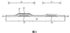
如图3所示,于基板10与第一层导电图案上形成一绝缘层30。绝缘层30是作为栅极绝缘层,其材质可为氧化硅或其它适合的介电材料。再于薄膜晶体管区12的绝缘层30上另形成一半导体层32与一重掺杂半导体层34。半导体层32作为通道,其材质可为硅(例如非晶硅),而重掺杂半导体层34则用来提高后续形成的源极与漏极与半导体层之间的奥姆式接触。As shown in FIG. 3 , an insulating
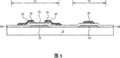
如图4所示,接着于绝缘层30上沉积一导电层,例如一金属层,并利用微影暨蚀刻技术定义此导电层以形成一第二层导电图案。第二层导电图案为金属材料,但亦可为其它导电材质,其包括一数据线40、一源极42与一漏极44。数据线40亦可为一直线,与扫描线20垂直交错并位于像素结构的另一边(如图1所示)。数据线40设置于遮光图案24的上方并对应遮光图案24,其中遮光图案24的宽度会略大于数据线40的宽度,用以遮蔽光线防止漏光,但遮光图案24的宽度与数据线40的宽度可视遮光需要作适度调整。源极42与漏极44亦设置于薄膜晶体管区12,且分别设置于栅极22二侧的上方并对应重掺杂半导体层34,并且源极42电连接至数据线40。As shown in FIG. 4 , a conductive layer, such as a metal layer, is then deposited on the insulating
如图5所示,随后于绝缘层30与第二层导电图案上形成一介电层50,再于介电层50上沉积一导电层(例如一金属层),并利用微影暨蚀刻技术定义此导电层以形成一第三层导电图案。介电层50的材质可为无机材质如氧化硅、氮化硅等,或是有机材质。第三层导电图案为金属材料,但亦可为其它导电材质,如氧化铟锡,其包含一贯穿像素结构的共通线61与一共通图案60,其共通图案60连接于共通线61,如图1所示。共通图案60含包两支线60a,此两支线60a位于像素结构的周边区14,并且两支线60a具有一间隙62,此两平行的支线60a亦可为两平行的直条。两支线60a分置于数据线40的两侧,其间隙62则位于数据线40的上方并且其间隙62至少大于或等于数据线40的宽度。As shown in FIG. 5, a
如图6所示,接着于介电层50与第三层导电图案上形成至少一保护层70,并去除部分保护层70与介电层50,以曝露出漏极44。如图7所示,随后于保护层70上形成一像素电极80,并使像素电极80与曝露出的漏极44电连接。As shown in FIG. 6 , at least one
本发明的像素结构具有三层金属层,其中第一导电图案的遮光图案24的作用在于遮蔽第二层导电图案的数据线40两侧容易产生的漏光,特别是斜向漏光,而第三层导电图案的作用在于利用共通图案60及部分共通线61屏蔽像素电极80与数据线40,以避免像素电极80与数据线40之间产生寄生电容,藉此可减少串音效应。值得注意的是,共通图案60本身为一具有一间隙62的两支线60a,而数据线40位于两支线60a之间,因此共通图案60本身却不会与数据线40产生过大的寄生电容。另外,共通图案60、像素电极80与位于其间保护层70亦可形成储存电容,使得像素结构不需另行于显示区内设置过大的储存电容,而可大幅提升开口率。The pixel structure of the present invention has three layers of metal layers, wherein the function of the light-shielding
于本实施例的像素结构中,共通图案60的两支线60a大体上与数据线40的两侧切齐,且由于遮光图案24的宽度大于数据线40的宽度,因此共通图案60与遮光图案24部分重叠,如图7所示,亦可形成储存电容。在综合考虑共通图案60的屏蔽效果、共通图案60与像素电极80之间的寄生电容值等因素下,本发明的像素结构亦可具有其它不同的实施方式,请参考相关的附图并配合下文说明,其中为彰显各实施例的特征,以下各附图仅绘示出周边区的剖面示意图,且各实施例相同组件使用相同组件符号标示并不再赘述。In the pixel structure of this embodiment, the two
请参考图8。图8为本发明另一较佳实施例的像素结构的剖面示意图。如图8所示,在本实施例中,共通图案60的两支线60a其中之一与数据线40的一侧部分重叠,而另一者则与数据线40的一侧切齐,而未与数据线40重叠。Please refer to Figure 8. FIG. 8 is a schematic cross-sectional view of a pixel structure according to another preferred embodiment of the present invention. As shown in FIG. 8 , in this embodiment, one of the two
请参考图9。图9为本发明又一较佳实施例的像素结构的剖面示意图。如图9所示,在本实施例中,共通图案60的两支线60a分别与数据线40相对应的一侧部分重叠。Please refer to Figure 9. FIG. 9 is a schematic cross-sectional view of a pixel structure in another preferred embodiment of the present invention. As shown in FIG. 9 , in this embodiment, the two
请参考图10。图10为本发明又一较佳实施例的像素结构的剖面示意图。如图5所示,在本实施例中,共通图案60的两支线60a均未与数据线40的两侧重叠,且各支线60a与数据线40对应的一侧间距有一距离。Please refer to Figure 10. FIG. 10 is a schematic cross-sectional view of a pixel structure in another preferred embodiment of the present invention. As shown in FIG. 5 , in this embodiment, neither of the two
上述实施例仅为本发明的不同实施方式,本发明的像素结构并不限于上述实施例所教导而可有其它变化,举例来说,遮光图案24、数据线40、共通图案60与像素电极80的相对位置可视需要作适度的变化。The above-mentioned embodiments are only different implementations of the present invention, and the pixel structure of the present invention is not limited to the teachings of the above-mentioned embodiments, and other changes are possible, for example, the light-shielding
综上所述,本发明的像素结构利用第一导电图案的遮光图案遮蔽第二层导电图案的数据线两侧容易产生的漏光,并利用第三层导电图案的共通图案屏蔽像素电极与数据线,以避免像素电极与数据线之间产生寄生电容。同时共通图案本身具有两平行的直条,且两直条之间具有对应于数据线之间隙,因此共通图案的两支线虽具有屏蔽像素电极与数据线的作用,但却不会与数据线产生过大的寄生电容,而可减少串音效应。再者,共通图案的两支线、像素电极与位于其间保护层亦可形成的储存电容,使得像素结构不需另行于显示区内设置过大的储存电容,使得本发明的像素结构具有超高开口率。In summary, the pixel structure of the present invention uses the light-shielding pattern of the first conductive pattern to shield the light leakage that is likely to occur on both sides of the data line of the second layer of conductive pattern, and uses the common pattern of the third layer of conductive pattern to shield the pixel electrode and the data line. to avoid parasitic capacitance between the pixel electrode and the data line. At the same time, the common pattern itself has two parallel straight bars, and there is a gap corresponding to the data line between the two straight bars. Therefore, although the two branch lines of the common pattern have the effect of shielding the pixel electrode and the data line, they will not interfere with the data line. Excessive parasitic capacitance can reduce crosstalk effects. Furthermore, the two branch lines of the common pattern, the pixel electrode and the protective layer in between can also form a storage capacitor, so that the pixel structure does not need to be additionally provided with an excessively large storage capacitor in the display area, so that the pixel structure of the present invention has an ultra-high opening. Rate.
以上所述仅为本发明的较佳实施例,凡依本发明申请专利范围所做的均等变化与修饰,皆应属本发明的涵盖范围。The above descriptions are only preferred embodiments of the present invention, and all equivalent changes and modifications made according to the scope of the patent application of the present invention shall fall within the scope of the present invention.
Claims (16)
Priority Applications (1)
| Application Number | Priority Date | Filing Date | Title |
|---|---|---|---|
| CN2008100045492ACN101221961B (en) | 2008-01-22 | 2008-01-22 | Pixel structure and manufacturing method thereof |
Applications Claiming Priority (1)
| Application Number | Priority Date | Filing Date | Title |
|---|---|---|---|
| CN2008100045492ACN101221961B (en) | 2008-01-22 | 2008-01-22 | Pixel structure and manufacturing method thereof |
Publications (2)
| Publication Number | Publication Date |
|---|---|
| CN101221961A CN101221961A (en) | 2008-07-16 |
| CN101221961Btrue CN101221961B (en) | 2010-06-23 |
Family
ID=39631675
Family Applications (1)
| Application Number | Title | Priority Date | Filing Date |
|---|---|---|---|
| CN2008100045492AActiveCN101221961B (en) | 2008-01-22 | 2008-01-22 | Pixel structure and manufacturing method thereof |
Country Status (1)
| Country | Link |
|---|---|
| CN (1) | CN101221961B (en) |
Families Citing this family (9)
| Publication number | Priority date | Publication date | Assignee | Title |
|---|---|---|---|---|
| CN101582423B (en)* | 2009-06-30 | 2011-01-05 | 友达光电股份有限公司 | Pixel structure and manufacturing method thereof |
| KR101730552B1 (en)* | 2010-04-13 | 2017-05-12 | 엘지디스플레이 주식회사 | In-Plane Switching Mode LCD and method of driving the same |
| CN103278971A (en)* | 2012-10-10 | 2013-09-04 | 上海天马微电子有限公司 | Thin film transistor array substrate and method of manufacturing the same |
| CN106773394B (en)* | 2016-10-14 | 2024-04-09 | 合肥京东方光电科技有限公司 | Array substrate, display panel and display device |
| CN107329339B (en)* | 2017-08-14 | 2020-04-07 | 深圳市华星光电技术有限公司 | Array substrate and curved surface liquid crystal display |
| TWI662349B (en)* | 2018-05-18 | 2019-06-11 | 友達光電股份有限公司 | Pixel structure |
| CN208737168U (en)* | 2018-09-30 | 2019-04-12 | 惠科股份有限公司 | Array substrate, display panel and display device |
| TWI692089B (en)* | 2019-04-09 | 2020-04-21 | 友達光電股份有限公司 | Display device |
| CN116449615B (en) | 2023-06-13 | 2023-10-03 | Tcl华星光电技术有限公司 | Display panel and display panel driving method |
Citations (2)
| Publication number | Priority date | Publication date | Assignee | Title |
|---|---|---|---|---|
| CN1677206A (en)* | 2004-03-30 | 2005-10-05 | Lg.菲利浦Lcd株式会社 | Liquid crystal display device |
| CN1987624A (en)* | 2006-11-17 | 2007-06-27 | 京东方科技集团股份有限公司 | TFT LCD array base board structure and its producing method |
- 2008
- 2008-01-22CNCN2008100045492Apatent/CN101221961B/enactiveActive
Patent Citations (2)
| Publication number | Priority date | Publication date | Assignee | Title |
|---|---|---|---|---|
| CN1677206A (en)* | 2004-03-30 | 2005-10-05 | Lg.菲利浦Lcd株式会社 | Liquid crystal display device |
| CN1987624A (en)* | 2006-11-17 | 2007-06-27 | 京东方科技集团股份有限公司 | TFT LCD array base board structure and its producing method |
Non-Patent Citations (3)
| Title |
|---|
| JP特开2004-77544A 2004.03.11 |
| JP特开2007-333835A 2007.12.27 |
| JP特开2007-334082A 2007.12.27 |
Also Published As
| Publication number | Publication date |
|---|---|
| CN101221961A (en) | 2008-07-16 |
Similar Documents
| Publication | Publication Date | Title |
|---|---|---|
| CN101221961B (en) | Pixel structure and manufacturing method thereof | |
| CN107316873B (en) | Array substrate and display device | |
| CN101825814B (en) | TFT (Thin Film Transistor)-LCD (Liquid Crystal Display) array baseplate and manufacturing method thereof | |
| CN103413812B (en) | Array base palte and preparation method thereof, display device | |
| CN100438048C (en) | Electrode structure in flat panel display, and fabricating method | |
| EP2953165B1 (en) | Oxide thin film transistor array substrate, manufacturing method thereof, and display panel | |
| CN100437306C (en) | TFT array circuit board and manufacturing method thereof | |
| CN103472646A (en) | Array substrate, manufacturing method thereof and display device | |
| TW200821721A (en) | Pixel structure and fabrication method thereof | |
| US20230178560A1 (en) | Thin-film transistor and method for manufacturing same, and array substrate and display panel | |
| CN112928125B (en) | Array substrate and display panel | |
| WO2014153958A1 (en) | Array substrate, method for manufacturing array substrate and display device | |
| CN102969311B (en) | Array substrate and manufacturing method thereof, and display device | |
| WO2023272503A1 (en) | Thin film transistor, preparation method therefor, display substrate, and display apparatus | |
| CN115810636A (en) | Metal oxide thin film transistor array substrate, manufacturing method thereof and display panel | |
| CN103094069A (en) | Pixel structure and manufacturing method thereof | |
| CN101799603B (en) | TFT-LCD array substrate and manufacture method thereof | |
| CN100447646C (en) | Pixel structure and manufacturing method thereof | |
| TWI328136B (en) | Pixel structure and method of making the same | |
| WO2021097995A1 (en) | Array substrate and preparation method therefor | |
| CN103681695B (en) | Thin-film transistor array base-plate, manufacture method and liquid crystal indicator | |
| CN101470307B (en) | Liquid crystal display device and manufacturing method thereof | |
| CN110034131A (en) | Array substrate and its manufacturing method, display panel and display device | |
| CN102487044A (en) | Array substrate, manufacturing method thereof, and electronic paper display | |
| CN101221926A (en) | Liquid crystal display unit structure and manufacturing method thereof |
Legal Events
| Date | Code | Title | Description |
|---|---|---|---|
| C06 | Publication | ||
| PB01 | Publication | ||
| C10 | Entry into substantive examination | ||
| SE01 | Entry into force of request for substantive examination | ||
| C14 | Grant of patent or utility model | ||
| GR01 | Patent grant |