CN101221629A - Smart card chip and method for placing input/output bonding pad - Google Patents
Smart card chip and method for placing input/output bonding padDownload PDFInfo
- Publication number
- CN101221629A CN101221629ACNA2008100022397ACN200810002239ACN101221629ACN 101221629 ACN101221629 ACN 101221629ACN A2008100022397 ACNA2008100022397 ACN A2008100022397ACN 200810002239 ACN200810002239 ACN 200810002239ACN 101221629 ACN101221629 ACN 101221629A
- Authority
- CN
- China
- Prior art keywords
- pads
- column
- pad
- smart card
- input
- Prior art date
- Legal status (The legal status is an assumption and is not a legal conclusion. Google has not performed a legal analysis and makes no representation as to the accuracy of the status listed.)
- Granted
Links
Images


Classifications
- G—PHYSICS
- G06—COMPUTING OR CALCULATING; COUNTING
- G06K—GRAPHICAL DATA READING; PRESENTATION OF DATA; RECORD CARRIERS; HANDLING RECORD CARRIERS
- G06K19/00—Record carriers for use with machines and with at least a part designed to carry digital markings
- G06K19/06—Record carriers for use with machines and with at least a part designed to carry digital markings characterised by the kind of the digital marking, e.g. shape, nature, code
- G06K19/067—Record carriers with conductive marks, printed circuits or semiconductor circuit elements, e.g. credit or identity cards also with resonating or responding marks without active components
- G06K19/07—Record carriers with conductive marks, printed circuits or semiconductor circuit elements, e.g. credit or identity cards also with resonating or responding marks without active components with integrated circuit chips
- H—ELECTRICITY
- H01—ELECTRIC ELEMENTS
- H01L—SEMICONDUCTOR DEVICES NOT COVERED BY CLASS H10
- H01L2924/00—Indexing scheme for arrangements or methods for connecting or disconnecting semiconductor or solid-state bodies as covered by H01L24/00
- H01L2924/0001—Technical content checked by a classifier
- H01L2924/0002—Not covered by any one of groups H01L24/00, H01L24/00 and H01L2224/00
Landscapes
- Engineering & Computer Science (AREA)
- Computer Hardware Design (AREA)
- Microelectronics & Electronic Packaging (AREA)
- Physics & Mathematics (AREA)
- General Physics & Mathematics (AREA)
- Theoretical Computer Science (AREA)
- Semiconductor Integrated Circuits (AREA)
Abstract
Description
Translated fromChinese技术领域technical field
本发明涉及智能卡(smart card)芯片,特别涉及智能卡内所使用芯片的输入/输出焊盘(pad)的配置,用以改善静电放电(electrostatic discharge,ESD)功能并减少芯片的布局面积。The present invention relates to a smart card chip, in particular to the configuration of the input/output pads of the chip used in the smart card to improve electrostatic discharge (electrostatic discharge, ESD) function and reduce the layout area of the chip.
背景技术Background technique
智能卡是一种内嵌集成电路(integrated circuit)芯片的塑胶卡片型式的卡,集成电路芯片可包括非易失性(non-volatile)存储器存储元件以及一些其他特定的安全逻辑电路。智能卡增强系统广泛使用在保健、银行业务、娱乐以及运输等范围。A smart card is a plastic card type card embedded with an integrated circuit chip, which may include non-volatile memory storage elements and some other specific security logic circuits. Smart card enhancement systems are widely used in healthcare, banking, entertainment, and transportation.
智能卡包括接触卡、无接触(contactless)卡以及混合(hybrid)卡。无接触卡使用射频(radio frequency,RF)来进行卡片与卡片读取器之间的传送。接触卡以及混合卡包括位于卡片外侧的一组电性接点,用以插入且耦接于卡片读取器。Smart cards include contact cards, contactless cards and hybrid cards. Contactless cards use radio frequency (RF) to communicate between the card and the card reader. Contact cards and hybrid cards include a set of electrical contacts on the outside of the card for insertion and coupling to the card reader.
智能卡传统上包括芯片,其中芯片包括微处理器以及可经由电性接点进行存取的存储器,例如:随机存取存储器(Random Access Memory,RAM)、只读存储器(Read Only Memory,ROM)以及电可擦可编程只读存储器(Electrically Erasable Programmable Read Only Memory,EEPROM)。接点提供电源、串行数据(serial data)传送的输入/输出、用以读取智能卡时钟(clock,CLK)信号的连接、用以复位(reset,RST)智能卡的连接以及智能卡的编程电压(programming voltage)的连接。这些接点的尺寸、功能以及位置由工业标准ISO 7816-2以及7816-3来规定(参考图1A)。上述标准可允许不同的制造商生产可互相兼容的智能卡以及装置。Smart cards traditionally include a chip, where the chip includes a microprocessor and memory that can be accessed through electrical contacts, such as: Random Access Memory (Random Access Memory, RAM), Read Only Memory (Read Only Memory, ROM) and electronic memory. Electrically Erasable Programmable Read Only Memory (EEPROM). The contacts provide power, input/output for serial data transmission, connections for reading the smart card clock (clock, CLK) signal, connections for resetting (reset, RST) the smart card, and programming voltage for the smart card (programming voltage) connection. The size, function and location of these contacts are specified by industry standards ISO 7816-2 and 7816-3 (see Figure 1A). The above-mentioned standards allow different manufacturers to produce smart cards and devices that are compatible with each other.
图1B示出智能卡的输入以及输出(I/O)焊盘的传统布局。然而,图1B布局中的主要缺点是需要越过芯片(cross-chip)的VDD/GND(或是图1B中VCC/GND)总线金属连接来提供足够的静电放电保护网络。越过芯片的VDD/GND总线金属连接会增加芯片的尺寸,所以不是令人满意的解决方案。FIG. 1B shows a conventional layout of input and output (I/O) pads of a smart card. However, the main disadvantage of the layout in Figure 1B is the need for a cross-chip VDD/GND (or VCC/GND in Figure 1B) bus metal connection to provide an adequate ESD protection network. Metal connections of the VDD/GND bus across the chip would increase the size of the chip, so it is not a satisfactory solution.
嵌入在智能卡内的芯片传统上是由互补金属氧化物半导体(complementary metal oxide semiconductor,CMOS)技术制造的,并需要免于受到静电放电的损害。当智能卡被到处携带、从皮夹内放入和取出并插入至卡片读取器时,静电电荷会累积在智能卡上。当足够的电荷累积在智能卡的特定尖端时,电荷将被传导至最低电位的电压(传统为接地端)。在累积电荷的尖端到较低电位的路径上,当电荷足够高时会损害芯片。与芯片所能承受的最大电压或电流相比,例如:金属氧化物半导体的栅极氧化物可能被仅略高于一般供应电压(5伏特、3.3伏特或甚至更低)的电压所破坏,由累积电荷所感应的电压和电流可能相当大,例如:2000伏特甚至更大的电压,或是越过1.5k欧姆的电阻的1.3安培以上甚至更大的电流。Chips embedded in smart cards are traditionally fabricated using complementary metal oxide semiconductor (CMOS) technology and need to be protected from damage from electrostatic discharge. Electrostatic charges can build up on smart cards as they are carried around, put in and out of wallets and inserted into card readers. When sufficient charge accumulates on a particular tip of the smart card, the charge is conducted to the lowest potential voltage (traditionally ground). On the way from the tip of the accumulated charge to a lower potential, the charge can damage the chip when it is high enough. Compared with the maximum voltage or current that the chip can withstand, for example: the gate oxide of metal oxide semiconductors may be damaged by voltages that are only slightly higher than the typical supply voltage (5 volts, 3.3 volts or even lower), by The voltage and current induced by the accumulated charge can be quite large, for example: 2000 volts or more, or 1.3 amps or more across a 1.5k ohm resistor.
传统上将静电放电保护电路加入到芯片的结合焊盘(bond pad)上,其中结合焊盘为提供芯片耦接至外部电路、电力供应、接地端以及电信号的连接。静电放电保护电路必须能够允许芯片正常操作,使得静电放电保护电路在芯片正常操作期间能有效地与芯片的核心电路隔离。Traditionally, an ESD protection circuit is added to a bond pad of a chip, wherein the bond pad provides connections for the chip to be coupled to external circuits, power supply, ground, and electrical signals. The ESD protection circuit must be able to allow the chip to operate normally, so that the ESD protection circuit can be effectively isolated from the core circuit of the chip during normal operation of the chip.
具有四种P型以及N型半导体材料可选择层的半导体元件或被称为可控硅整流器(silicon controlled rectifier,SCR)的PNPN元件可以是静电放电保护电路中能防止静电放电产生损害的最有效的元件之一。可控硅整流器操作在两种模式:阻隔(blocking)模式以及闩锁(latch up)模式。在阻隔模式中,可控硅整流器会阻挡电流通过,使得静电放电保护电路不会对要被保护的核心电路造成影响。当可控硅整流器内有足够的电流再生时,闩锁情况被触发。闩锁出现在互补寄生双极性晶体管结构中,其传统上存在于互补金属氧化物半导体结构内。既然互补寄生双极性晶体管非常靠近,互补双极性结构即能互相电性作用,从而形成动作表现如PNPN二极管的元件结构。静电放电事件中,大电流能流经可控硅整流器从而越过核心电路。A semiconductor element with four optional layers of P-type and N-type semiconductor materials or a PNPN element called a silicon controlled rectifier (SCR) can be the most effective way to prevent damage caused by electrostatic discharge in an electrostatic discharge protection circuit. one of the components. SCRs operate in two modes: blocking mode and latch up mode. In blocking mode, the silicon controlled rectifier will block the flow of current, so that the electrostatic discharge protection circuit will not affect the core circuit to be protected. The latch-up condition is triggered when sufficient current is regenerated in the SCR. Latch-up occurs in complementary parasitic bipolar transistor structures, which are traditionally found in complementary metal-oxide-semiconductor structures. Since the complementary parasitic bipolar transistors are in close proximity, the complementary bipolar structures can electrically interact with each other to form a device structure that behaves like a PNPN diode. During an ESD event, large currents can flow through the silicon controlled rectifier across the core circuitry.
然而,无论使用何种结构作为静电放电保护电路,智能卡上的传统芯片还是必须包括会增加芯片尺寸的越过芯片的VDD/GND总线金属连接(参考图1B)。However, no matter what structure is used as the ESD protection circuit, conventional chips on smart cards still have to include VDD/GND bus metal connections across the chip which increase chip size (see FIG. 1B ).
因此,在智能卡设计的技术中,需要能够对智能卡内所使用的芯片的输入/输出焊盘提供有效空间布局的新设计。Therefore, in the art of smart card design, there is a need for a new design capable of providing an efficient spatial layout of the input/output pads of the chip used in the smart card.
发明内容Contents of the invention
本发明涉及智能卡芯片,特别涉及智能卡内所使用芯片的输入/输出焊盘的配置,用以改善静电放电功能并减少芯片的布局面积。仅作为示例来说,本发明可用于智能卡内所使用的芯片上。然而,本领域技术人员可认识到,本发明还具有更大范围的实用性。The invention relates to a smart card chip, in particular to the configuration of the input/output pads of the chip used in the smart card, which is used to improve the electrostatic discharge function and reduce the layout area of the chip. By way of example only, the invention can be used on chips used in smart cards. However, those skilled in the art will recognize that the present invention has broader applicability.
在一个特定实施例中,本发明提供一种具有新输入/输出焊盘配置的智能卡芯片。在一个实施例中,智能卡芯片包括核心电路。芯片还包括对应于上述电性接点的多个输入/输出焊盘,其中上述输入/输出焊盘划分成至少一个第一列以及放置成与上述第一列直接相邻的第二列,使得上述第一列以及上述第二列形成丛聚。In a particular embodiment, the present invention provides a smart card chip with a new input/output pad configuration. In one embodiment, the smart card chip includes core circuitry. The chip also includes a plurality of input/output pads corresponding to the above-mentioned electrical contacts, wherein the above-mentioned I/O pads are divided into at least one first column and a second column placed directly adjacent to the above-mentioned first column, so that the above-mentioned The first column and the aforementioned second column form clusters.
上述智能卡芯片中,第一列或第二列可具有至少四个输入/输出焊盘。In the above smart card chip, the first column or the second column may have at least four input/output pads.
上述智能卡芯片中,丛聚可被核心电路的三个邻近侧部分地包围。In the smart card chip described above, the cluster may be partially surrounded by three adjacent sides of the core circuit.
上述智能卡芯片中,多个输入/输出焊盘可包括电源焊盘、接地焊盘、串行数据传送焊盘、时钟信号焊盘、复位焊盘、冗余电源焊盘以及冗余接地焊盘,并且所述输入/输出焊盘放置在所述丛聚内,以使得串行数据传送焊盘、时钟信号焊盘以及复位焊盘被电源焊盘、冗余电源焊盘、接地焊盘以及冗余接地焊盘部分地围住。In the above smart card chip, the multiple input/output pads may include power pads, ground pads, serial data transmission pads, clock signal pads, reset pads, redundant power pads, and redundant ground pads, And the I/O pads are placed in the cluster so that the serial data transfer pads, clock signal pads, and reset pads are replaced by power pads, redundant power pads, ground pads, and redundant The ground pad is partially enclosed.
上述智能卡芯片还可包括:VDD/GND保护环结构,用于防止闩锁;以及至少一个或多边缘单元,具有VDD/GND保护环结构。The smart card chip above may further include: a VDD/GND guard ring structure for preventing latch-up; and at least one or more edge units with a VDD/GND guard ring structure.
在另一个实施例中,公开一种放置输入/输出焊盘的方法,适用于包括核心电路以及与智能卡读取器传送数据的多个输入/输出焊盘的智能卡芯片。上述方法包括将上述输入/输出焊盘划分成至少一个第一列以及第二列,上述第一列以及上述第二列具有相同数量的输入/输出焊盘。上述方法还包括将上述第一列以及上述第二列放置成彼此直接相邻,以在上述核心电路内形成丛聚。In another embodiment, a method of placing I/O pads for a smart card chip including a core circuit and a plurality of I/O pads for communicating data with a smart card reader is disclosed. The method includes dividing the input/output pads into at least a first column and a second column, the first column and the second column having the same number of input/output pads. The method also includes placing the first column and the second column directly adjacent to each other to form clusters within the core circuit.
上述放置输入/输出焊盘的方法中,丛聚可被核心电路的至少三个邻近侧部分地包围。In the above method of placing input/output pads, the cluster may be partially surrounded by at least three adjacent sides of the core circuit.
上述放置输入/输出焊盘的方法中,第一列可包括至少一个接地焊盘以及串行数据传送焊盘。In the above method for placing input/output pads, the first column may include at least one ground pad and a serial data transmission pad.
上述放置输入/输出焊盘的方法中,第二列可包括至少一个电源焊盘、复位焊盘以及时钟信号焊盘。In the above method of placing input/output pads, the second column may include at least one power pad, reset pad and clock signal pad.
上述放置输入/输出焊盘的方法中,接地焊盘以及电源焊盘可放置成彼此直接相邻,以减少电源或接地总线的绕线面积,并通过减少电源或接地总线的电阻来改善静电放电的功能。In the above method of placing I/O pads, the ground pad and the power pad can be placed directly adjacent to each other to reduce the power or ground bus winding area and improve electrostatic discharge by reducing the resistance of the power or ground bus function.
上述放置输入/输出焊盘的方法中,丛聚还可包括冗余接地焊盘以及冗余电源焊盘。In the above method of placing input/output pads, the cluster may further include redundant ground pads and redundant power pads.
上述放置输入/输出焊盘的方法中,输入/输出焊盘可放置在丛聚内,以使得串行数据传送焊盘、时钟信号焊盘以及复位焊盘被电源供应焊盘、冗余电源供应焊盘、接地焊盘以及冗余接地焊盘部分地围住。In the above method of placing the I/O pads, the I/O pads can be placed in the cluster so that the serial data transfer pads, the clock signal pads, and the reset pads are replaced by the power supply pads, redundant power supply pads, etc. pads, ground pads, and redundant ground pads are partially enclosed.
上述放置输入/输出焊盘的方法中,丛聚还可包括至少一个或多个测试焊盘,以及来自电压稳压器的输入的焊盘,以允许容易地与芯片内电压稳压器整合。In the above method of placing I/O pads, the cluster may further include at least one or more test pads, and pads for inputs from voltage regulators to allow easy integration with on-chip voltage regulators.
上述放置输入/输出焊盘的方法中,丛聚还可包括至少一个或多个边缘单元,具有保护环结构以防止闩锁。In the above method of placing I/O pads, the cluster may further include at least one or more edge cells having a guard ring structure to prevent latch-up.
在又一个实施例中,芯片包括静电放电网络,其包括电性连接至上述电源焊盘的至少一个VDD总线,以及电性连接至上述接地焊盘的至少一个GND总线,上述VDD总线与上述GND总线被放置成大体上平行于上述输入/输出焊盘的上述列。上述VDD总线可被放置在上述cluster的各侧且上述GND总线被放置在上述列之间,其中各上述输入/输出焊盘经由静电放电单元而至少耦接至上述GND总线或VDD总线,因此提供从上述输入/输出焊盘至上述GND总线或VDD总线直至接地端的短路径。In yet another embodiment, the chip includes an electrostatic discharge network, which includes at least one VDD bus electrically connected to the power pad, and at least one GND bus electrically connected to the ground pad, the VDD bus and the GND The bus lines are placed substantially parallel to the aforementioned columns of input/output pads. The VDD bus may be placed on each side of the cluster and the GND bus may be placed between the columns, wherein each of the input/output pads is at least coupled to the GND bus or the VDD bus via an electrostatic discharge unit, thus providing A short path from the above I/O pad to the above GND bus or VDD bus to ground.
对客户芯片而言,既然不需要越过芯片的VDD/GND总线连接,所以优于传统相关技术的新配置的优点之一是芯片尺寸至少可减少3%至5%。另一个优点包括本发明可改善静电放电功能。既然丛聚可被放置在芯片内的任何地方,因此可容易地与芯片内电压稳压器整合。For the customer chip, one of the advantages of the new configuration over the conventional related art is that the chip size can be reduced by at least 3% to 5% since there is no need for a VDD/GND bus connection across the chip. Another advantage includes that the present invention improves electrostatic discharge performance. Since clusters can be placed anywhere within the chip, they can be easily integrated with on-chip voltage regulators.
附图说明Description of drawings
图1A示出根据ISO标准的智能卡接点的简单布局图;Figure 1A shows a simple layout of smart card contacts according to the ISO standard;
图1B示出智能卡芯片中输入/输出焊盘的传统配置的简单布局图;Figure 1B shows a simple layout diagram of a traditional configuration of input/output pads in a smart card chip;
图2示出根据本发明一个实施例所述智能卡芯片中输入/输出焊盘的配置的简单布局图;Fig. 2 shows a simple layout diagram of the configuration of input/output pads in the smart card chip according to an embodiment of the present invention;
图3示出根据本发明另一个实施例所述智能卡芯片中输入/输出焊盘的配置的放大布局图;以及3 shows an enlarged layout diagram of the configuration of the input/output pads in the smart card chip according to another embodiment of the present invention; and
图4示出根据本发明又一个实施例所述智能卡芯片中输入/输出焊盘的配置以及静电放电网络的简单布局图。Fig. 4 shows the configuration of the input/output pads and the simple layout of the electrostatic discharge network in the smart card chip according to another embodiment of the present invention.
其中,附图标记说明如下:Wherein, the reference signs are explained as follows:
1-8~电性接点1-8~electrical contacts
10-11~距离10-11~distance
100~图示100~Illustrated
102、200~芯片102, 200~chip
21-28、41-48~输入/输出焊盘21-28, 41-48~input/output pads
29、30~列29, 30 ~ column
31、51~核心电路31, 51~core circuit
32、52~存储器元件32, 52 ~ memory element
33、34~越过芯片的VDD/GND总线连接33, 34 ~ VDD/GND bus connection across the chip
400~布局视图400~Layout view
49、300~丛聚49, 300~clustering
61-65、70~焊盘61-65, 70~pad
68~冗余接地焊盘68~Redundant ground pad
69~冗余电源焊盘69~redundant power pad
71、72~测试焊盘71, 72~Test pads
73~丛聚边缘单元73~cluster edge unit
80~静电放电网络80~ESD network
81、82~VDD总线81, 82 ~ VDD bus
83~GND总线83~GND bus
86-97~静电放电保护元件86-97~ESD protection components
9~智能卡边缘9 ~ smart card edge
具体实施方式Detailed ways
为让本发明的上述和其他目的、特征、和优点能更明显易懂,下文特举出较佳实施例,并配合所附图式,作详细说明如下:In order to make the above and other objects, features, and advantages of the present invention more comprehensible, the preferred embodiments are specifically listed below, together with the accompanying drawings, and are described in detail as follows:
实施例:Example:
图1A示出根据ISO标准的智能卡接点的简单布局图。如图1A所示,图示100示出ISO标准中与智能卡边缘9的电性接点1-8相关的配置。接点1与接点5被设计成耦接至供应电源以及接地端。接点7作为串行数据的输入/输出焊盘。接点3作为用以读出智能卡时钟信号的连接。接点2作为用以复位智能卡的连接,而接点6用于智能卡的编程电压的连接。接点的配置分别由从智能卡上边以及左边的一组距离10与距离11来决定。接点4以及接点8保留给将来使用。Figure 1A shows a simple layout of smart card contacts according to the ISO standard. As shown in FIG. 1A , diagram 100 shows the configuration related to the electrical contacts 1 - 8 of the
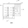
图1B示出智能卡芯片中输入/输出焊盘的传统配置的简单布局图。图1A所示出的ISO标准接点1-8的配置会导致如图1B所示的智能卡芯片的输入/输出焊盘的传统配置。传统上,芯片102具有位于芯片102边缘、划分成列(column)29与列30、并由核心电路31分隔的输入/输出焊盘21-28。FIG. 1B shows a simple layout diagram of a conventional configuration of input/output pads in a smart card chip. The configuration of ISO standard contacts 1-8 shown in FIG. 1A would result in the conventional configuration of I/O pads of a smart card chip as shown in FIG. 1B. Conventionally, chip 102 has I/O pads 21 - 28 located at the edge of chip 102 , divided into
芯片102还包括存储器元件32。核心电路31与存储器元件32均对静电放电非常敏感,因此芯片102也必须包括由越过芯片的VDD/GND总线连接33、34构成的足够的静电放电保护电路。上述越过芯片的VDD/GND总线连接会显著增加芯片的总面积以及总线电阻。Chip 102 also includes memory element 32 . Both core circuitry 31 and memory elements 32 are very sensitive to ESD, so chip 102 must also include adequate ESD protection circuitry consisting of VDD/GND bus connections 33, 34 across the chip. The above-mentioned VDD/GND bus connection across the chip will significantly increase the total area of the chip and the bus resistance.
图2示出根据本发明一个实施例的智能卡芯片中输入/输出焊盘的配置的简单布局图。参考图2,其示出智能卡的输入/输出焊盘41-48的布局。与传统配置相比,列29与列30(参考图1B)被放置成彼此直接紧邻,并组成丛聚(cluster)49。通过修改核心电路51的形状,就能部分地包围丛聚49(以及输入/输出焊盘41-48)。芯片200还包括存储器元件52。全部的输入/输出焊盘41-48还聚集在丛聚49的相连区域内。Fig. 2 shows a simple layout diagram of the configuration of input/output pads in a smart card chip according to an embodiment of the present invention. Referring to Figure 2, there is shown the layout of the input/output pads 41-48 of the smart card. In contrast to conventional configurations, columns 29 and 30 (see FIG. 1B ) are placed directly next to each other and form a cluster 49 . By modifying the shape of core circuit 51, cluster 49 (and input/output pads 41-48) can be partially surrounded. Chip 200 also includes memory element 52 . All input/output pads 41 - 48 are also grouped in the contiguous area of cluster 49 .
图3示出根据本发明另一个实施例的智能卡芯片中输入/输出焊盘的配置的放大布局图。丛聚300包括作为电源(VDD)的焊盘61、用以复位芯片的焊盘62(RST)、用以读取芯片的脉冲信号的焊盘63(CLK)、作为接地端的焊盘64,以及与芯片传送串行数据的焊盘65(IO)。然而,与图2中的丛聚49相比,丛聚300额外地包括冗余接地焊盘(Dummy GND)68、冗余电源焊盘(Dummy VDD)69、作为来自电压稳压器的输入的焊盘70(VDDC)以及测试焊盘71(TEST PAD 1)与测试焊盘72(TEST PAD 2)。丛聚边缘单元73包括VDD/GND保护环(guard ring)结构以防止闩锁现象。FIG. 3 shows an enlarged layout diagram of a configuration of input/output pads in a smart card chip according to another embodiment of the present invention. The
如图3所示,分别作为电源以及接地的焊盘61与焊盘64被放置成背对背。增加冗余接地焊盘68以及冗余电源焊盘69以改善静电放电保护功能,使得焊盘62、焊盘63与焊盘65被VDD/GND焊盘(焊盘61、64)以及冗余VDD/GND焊盘(焊盘68、69)所包围。As shown in FIG. 3 ,
图4示出根据本发明另一个实施例的智能卡芯片中输入/输出焊盘的配置以及静电放电网络的简单布局图。图4示出图3中智能卡芯片内输入/输出焊盘的配置以及静电放电网络80的布局视图400。静电放电网络80包括作为主要静电放电总线的VDD总线81、82以及GND总线83。静电放电网络80还包括多个静电放电保护元件86-97(例如可控硅整流器),静电放电保护元件86-97分别耦接于焊盘61-68以及VDD总线81、82与GND总线83之间,用以例如当使用者意外地接触到智能卡的接触点时,保护各输入/输出端免于任何意外的静电放电。FIG. 4 shows a configuration of input/output pads and a simple layout diagram of an electrostatic discharge network in a smart card chip according to another embodiment of the present invention. FIG. 4 shows a
可以了解到,包括焊盘64、65的第一组结合焊盘以及包括焊盘61-63的第二组结合焊盘被静电放电金属总线(GND)包围在两侧。耦接于第一组结合焊盘以及第二组结合焊盘之间的静电放电金属总线(VDD)经由背对背的VDD/GND与冗余VDD/GND与边缘单元相邻。与现有技术相比,上述设计提供变短的全面静电放电路径以将电荷传导至接地端。本领域技术人员可认识到,VDD总线以及GND总线越短,则电阻越低且放电速度越快。It can be appreciated that the first group of bonding
本发明排除了对于越过芯片的VDD/GND总线连接的需要,因此大幅地减少了芯片尺寸(在客户芯片上大约减少3%至5%),而仍然提供极佳的静电放电功能。由于VDD总线以及GND总线的电阻减少,本发明还提供较佳的静电放电保护功能,且没有限定芯片内丛聚的配置。另外,本发明能够容易地与芯片内电压稳压器(voltage regulator,VR)整合,以提供额外的冗余接地焊盘以及其他电源焊盘,如图3所示。The present invention eliminates the need for a VDD/GND bus connection across the chip, thus reducing the chip size dramatically (approximately 3% to 5% on customer chips), while still providing excellent ESD capability. Due to the reduced resistance of the VDD bus and the GND bus, the present invention also provides a better ESD protection function, and does not limit the configuration of clusters in the chip. In addition, the present invention can be easily integrated with an on-chip voltage regulator (VR) to provide additional redundant ground pads and other power pads, as shown in FIG. 3 .
上述说明提供许多不同的实施例或是用以实施本发明不同特征的实施例。描述构成以及步骤的特定实施例可帮助理解本发明。当然,上述说明只是实施例,并没有打算在权利要求意义上限定本发明。The above description provides many different embodiments or embodiments for implementing various features of the invention. Specific embodiments describing components and steps are helpful in understanding the present invention. Of course, the above descriptions are examples only, and are not intended to limit the invention in the sense of the claims.
本发明虽以优选实施例公开如上,然而所公开内容并非用以限定本发明的范围,任何本领域技术人员,在不脱离本发明的精神和范围内,当可做一定的更动与修改,因此本发明的保护范围应以所附权利要求为准。Although the present invention is disclosed above with preferred embodiments, the disclosed content is not intended to limit the scope of the present invention. Anyone skilled in the art can make certain changes and modifications without departing from the spirit and scope of the present invention. Therefore, the protection scope of the present invention should be determined by the appended claims.
Claims (15)
Translated fromChineseApplications Claiming Priority (2)
| Application Number | Priority Date | Filing Date | Title |
|---|---|---|---|
| US11/651,870US8079528B2 (en) | 2007-01-10 | 2007-01-10 | Input/output pads placement for a smart card chip |
| US11/651,870 | 2007-01-10 |
Publications (2)
| Publication Number | Publication Date |
|---|---|
| CN101221629Atrue CN101221629A (en) | 2008-07-16 |
| CN101221629B CN101221629B (en) | 2010-12-29 |
Family
ID=39593420
Family Applications (1)
| Application Number | Title | Priority Date | Filing Date |
|---|---|---|---|
| CN2008100022397AExpired - Fee RelatedCN101221629B (en) | 2007-01-10 | 2008-01-02 | Smart card chip and method for placing input/output bonding pad |
Country Status (2)
| Country | Link |
|---|---|
| US (1) | US8079528B2 (en) |
| CN (1) | CN101221629B (en) |
Cited By (3)
| Publication number | Priority date | Publication date | Assignee | Title |
|---|---|---|---|---|
| CN104866891A (en)* | 2015-06-02 | 2015-08-26 | 苏州海博智能系统有限公司 | Intelligent card with electrostatic protection |
| CN109195318A (en)* | 2018-10-26 | 2019-01-11 | 科大智能电气技术有限公司 | The method and PCB pad of one kind of multiple network switchings encapsulate |
| WO2020087427A1 (en)* | 2018-11-01 | 2020-05-07 | Yangtze Memory Technologies Co., Ltd. | Integrated circuit electrostatic discharge bus structure and related method |
Families Citing this family (13)
| Publication number | Priority date | Publication date | Assignee | Title |
|---|---|---|---|---|
| US7986504B2 (en)* | 2009-03-24 | 2011-07-26 | Arm Limited | Distributing power to an integrated circuit |
| US8649820B2 (en) | 2011-11-07 | 2014-02-11 | Blackberry Limited | Universal integrated circuit card apparatus and related methods |
| USD703208S1 (en) | 2012-04-13 | 2014-04-22 | Blackberry Limited | UICC apparatus |
| US8936199B2 (en) | 2012-04-13 | 2015-01-20 | Blackberry Limited | UICC apparatus and related methods |
| USD701864S1 (en) | 2012-04-23 | 2014-04-01 | Blackberry Limited | UICC apparatus |
| USD759022S1 (en) | 2013-03-13 | 2016-06-14 | Nagrastar Llc | Smart card interface |
| USD758372S1 (en) | 2013-03-13 | 2016-06-07 | Nagrastar Llc | Smart card interface |
| US9888283B2 (en) | 2013-03-13 | 2018-02-06 | Nagrastar Llc | Systems and methods for performing transport I/O |
| USD729808S1 (en) | 2013-03-13 | 2015-05-19 | Nagrastar Llc | Smart card interface |
| US9647997B2 (en) | 2013-03-13 | 2017-05-09 | Nagrastar, Llc | USB interface for performing transport I/O |
| USD780763S1 (en) | 2015-03-20 | 2017-03-07 | Nagrastar Llc | Smart card interface |
| USD864968S1 (en) | 2015-04-30 | 2019-10-29 | Echostar Technologies L.L.C. | Smart card interface |
| DE102016110780B4 (en)* | 2016-06-13 | 2024-10-10 | Infineon Technologies Austria Ag | Chip card module and method for producing a chip card module |
Family Cites Families (41)
| Publication number | Priority date | Publication date | Assignee | Title |
|---|---|---|---|---|
| US4727246A (en)* | 1984-08-31 | 1988-02-23 | Casio Computer Co., Ltd. | IC card |
| JPS6478397A (en)* | 1987-09-18 | 1989-03-23 | Mitsubishi Electric Corp | Ic card writing system |
| US5300765A (en)* | 1990-03-19 | 1994-04-05 | Mitsubishi Denki Kabushiki Kaisha | Memory card with latch-up protection |
| JPH05294093A (en)* | 1991-03-22 | 1993-11-09 | Toshiba Corp | Portable memory medium |
| FR2686997B1 (en)* | 1992-01-30 | 1994-04-01 | Gemplus Card International | TWO - CONTACTING CHIP CARD AND METHOD FOR COMMUNICATING WITH A CARD READER. |
| JP3477781B2 (en)* | 1993-03-23 | 2003-12-10 | セイコーエプソン株式会社 | IC card |
| EP0623958B1 (en)* | 1993-05-04 | 1998-04-01 | Siemens Aktiengesellschaft | Semi-conductor integrated circuit including protection means |
| US5581065A (en)* | 1993-08-02 | 1996-12-03 | Dai Nippon Printing Co., Ltd. | Sheet-framed IC carrier, method for producing the same, and IC carrier case |
| US5932866A (en)* | 1995-05-19 | 1999-08-03 | Dai Nippon Printing Co., Ltd. | Optical card with a built-in IC module technical field |
| DE19541072A1 (en)* | 1995-11-03 | 1997-05-07 | Siemens Ag | Chip module |
| US5837153A (en)* | 1997-01-15 | 1998-11-17 | Kawan; Joseph C. | Method and system for creating and using a logotype contact module with a smart card |
| US6581122B1 (en)* | 1998-03-26 | 2003-06-17 | Gemplus | Smart card which operates with the USB protocol |
| US6151202A (en)* | 1999-03-18 | 2000-11-21 | International Business Machines Corporation | Discharging electrostatic charge during hot card insertion |
| EP1095356B1 (en)* | 1999-05-14 | 2011-07-20 | Robert Bosch Gmbh | Contact arrangement and counter-contact module |
| DE19950524A1 (en)* | 1999-10-20 | 2001-04-26 | Philips Corp Intellectual Pty | Smart card |
| JP3822768B2 (en)* | 1999-12-03 | 2006-09-20 | 株式会社ルネサステクノロジ | IC card manufacturing method |
| JP3815936B2 (en)* | 2000-01-25 | 2006-08-30 | 株式会社ルネサステクノロジ | IC card |
| EP1146560B1 (en)* | 2000-04-12 | 2006-12-06 | Infineon Technologies AG | ESD Latch-up protection circuit for an integrated circuit |
| WO2001084490A1 (en)* | 2000-04-28 | 2001-11-08 | Hitachi,Ltd | Ic card |
| US6439464B1 (en)* | 2000-10-11 | 2002-08-27 | Stmicroelectronics, Inc. | Dual mode smart card and associated methods |
| US6538288B2 (en)* | 2000-11-29 | 2003-03-25 | Winbond Electronics Corp. | ESD protection device with island-like distributed p+ diffusion regions |
| US6634565B2 (en)* | 2001-11-06 | 2003-10-21 | Litronic, Inc. | Smart card having additional connector pads |
| EP1612711B1 (en)* | 2002-05-24 | 2007-03-21 | NTT DoCoMo, Inc. | Terminal interface for chipcards |
| JP3866178B2 (en)* | 2002-10-08 | 2007-01-10 | 株式会社ルネサステクノロジ | IC card |
| US6752321B1 (en)* | 2003-03-31 | 2004-06-22 | Stmicroelectronics, Inc. | Smart card and method that modulates multi-color LED indicative of operational attributes and/or transactions between the smart card and USB port of a USB host |
| JP4037332B2 (en)* | 2003-07-10 | 2008-01-23 | シャープ株式会社 | IC module and IC card |
| JP2005322109A (en)* | 2004-05-11 | 2005-11-17 | Renesas Technology Corp | Ic card module |
| US7411767B2 (en)* | 2004-06-02 | 2008-08-12 | Taiwan Semiconductor Manufacturing Company, Ltd. | Multi-domain ESD protection circuit structure |
| US7325724B2 (en)* | 2004-07-01 | 2008-02-05 | American Express Travel Related Services Company, Inc. | Method for registering a biometric for use with a smartcard |
| US20060016869A1 (en)* | 2004-07-01 | 2006-01-26 | American Express Travel Related Services Company, Inc. | Method and system for auditory emissions recognition biometrics on a smartcard |
| US7420250B2 (en)* | 2004-08-30 | 2008-09-02 | Taiwan Semiconductor Manufacturing Company, Ltd. | Electrostatic discharge protection device having light doped regions |
| US7360713B2 (en)* | 2004-09-24 | 2008-04-22 | Renesas Technology Corp. | Semiconductor device |
| US7323752B2 (en)* | 2004-09-30 | 2008-01-29 | Taiwan Semiconductor Manufacturing Co., Ltd. | ESD protection circuit with floating diffusion regions |
| US20060081968A1 (en)* | 2004-10-15 | 2006-04-20 | Bai Shwang S | Semiconductor package |
| EP1772794A1 (en)* | 2005-10-10 | 2007-04-11 | Axalto S.A. | Method and circuit for local clock generation and smartcard including it thereon |
| DE102005049256A1 (en)* | 2005-10-14 | 2007-04-26 | Infineon Technologies Ag | Chip card module has card contacts with contact surface and chip on opposite side from contact surface with integrated circuit and contacts at least partly connected to card contacts |
| ATE462168T1 (en)* | 2005-12-22 | 2010-04-15 | Lg Electronics Inc | METHOD FOR MORE EFFICIENT USE OF AN INTERFACE BETWEEN A CHIP CARD AND A DEVICE, ASSOCIATED CHIP CARD AND DEVICE |
| WO2007097775A1 (en)* | 2006-02-24 | 2007-08-30 | American Bank Note Holographics, Inc. | Method of reducing electro-static discharge (esd) from conductors on insulators |
| DE102006016419A1 (en)* | 2006-04-07 | 2007-10-18 | Infineon Technologies Ag | Smart card module and method for protecting a smart card module from overvoltages |
| KR100939067B1 (en)* | 2006-07-07 | 2010-01-28 | 삼성전자주식회사 | Smart card with multiple different interfaces |
| US8049250B2 (en)* | 2008-10-27 | 2011-11-01 | Taiwan Semiconductor Manufacturing Company, Ltd. | Circuit and method for power clamp triggered dual SCR ESD protection |
- 2007
- 2007-01-10USUS11/651,870patent/US8079528B2/ennot_activeExpired - Fee Related
- 2008
- 2008-01-02CNCN2008100022397Apatent/CN101221629B/ennot_activeExpired - Fee Related
Cited By (7)
| Publication number | Priority date | Publication date | Assignee | Title |
|---|---|---|---|---|
| CN104866891A (en)* | 2015-06-02 | 2015-08-26 | 苏州海博智能系统有限公司 | Intelligent card with electrostatic protection |
| CN109195318A (en)* | 2018-10-26 | 2019-01-11 | 科大智能电气技术有限公司 | The method and PCB pad of one kind of multiple network switchings encapsulate |
| CN109195318B (en)* | 2018-10-26 | 2021-03-02 | 科大智能电气技术有限公司 | Method for switching multiple networks and PCB pad package |
| WO2020087427A1 (en)* | 2018-11-01 | 2020-05-07 | Yangtze Memory Technologies Co., Ltd. | Integrated circuit electrostatic discharge bus structure and related method |
| CN111199891A (en)* | 2018-11-01 | 2020-05-26 | 长江存储科技有限责任公司 | Integrated circuit electrostatic discharge bus structure and related method |
| US10879164B2 (en) | 2018-11-01 | 2020-12-29 | Yangtze Memory Technologies Co., Ltd. | Integrated circuit electrostatic discharge bus structure and related method |
| CN111199891B (en)* | 2018-11-01 | 2021-03-12 | 长江存储科技有限责任公司 | Integrated circuit electrostatic discharge bus structure and related method |
Also Published As
| Publication number | Publication date |
|---|---|
| CN101221629B (en) | 2010-12-29 |
| US8079528B2 (en) | 2011-12-20 |
| US20080164324A1 (en) | 2008-07-10 |
Similar Documents
| Publication | Publication Date | Title |
|---|---|---|
| CN101221629B (en) | Smart card chip and method for placing input/output bonding pad | |
| KR102705228B1 (en) | Area-efficient and robust electrostatic discharge circuit | |
| US20030007298A1 (en) | Electrostatic discharge protective circuit | |
| TW200302627A (en) | Semiconductor integrated circuit apparatus | |
| CN106601717A (en) | Semiconductor chip module and semiconductor package including the same | |
| CN107408533B (en) | Semiconductor device | |
| US20030235019A1 (en) | Electrostatic discharge protection scheme for flip-chip packaged integrated circuits | |
| JP2011060303A (en) | Device with integrated circuit made secure by attenuation of electronic signatures | |
| CN107112281B (en) | Semiconductor device and design method thereof | |
| US11004521B2 (en) | Semiconductor device and semiconductor memory device | |
| US20110045645A1 (en) | High-efficiency filler cell with switchable, integrated buffer capacitance for high frequency applications | |
| US11152314B2 (en) | Integrated circuit with supply circuit comprising field-effect transistors | |
| KR20170132371A (en) | Semiconductor Integrated Circuit Device Having Circuit For Electrostatic Discharge Protection | |
| JP4403372B2 (en) | Data communication device | |
| CN102945823B (en) | Method for reducing area of interconnected input-output pins on stacked chips | |
| US6628488B2 (en) | Electrostatic discharge protection circuit | |
| EP3929982A1 (en) | Integrated circuit device including electrostatic discharge protection and current limiting circuitry | |
| CN114362482B (en) | Pin input circuit and chip | |
| KR101679347B1 (en) | Semiconductor device | |
| KR100942956B1 (en) | Electrostatic Discharge Device Using SRC Circuit | |
| US20250158392A1 (en) | Semiconductor device | |
| KR200443273Y1 (en) | Functional unit interface circuit of multi-chip system | |
| CN212874490U (en) | ESD protection device on EEPROM chip | |
| US20250076368A1 (en) | Semiconductor package | |
| CN116864495A (en) | A communication chip and electronic device |
Legal Events
| Date | Code | Title | Description |
|---|---|---|---|
| C06 | Publication | ||
| PB01 | Publication | ||
| C10 | Entry into substantive examination | ||
| SE01 | Entry into force of request for substantive examination | ||
| C14 | Grant of patent or utility model | ||
| GR01 | Patent grant | ||
| CF01 | Termination of patent right due to non-payment of annual fee | ||
| CF01 | Termination of patent right due to non-payment of annual fee | Granted publication date:20101229 |