CN101213531A - Memory controller interface for memory access with micro-stitching - Google Patents
Memory controller interface for memory access with micro-stitchingDownload PDFInfo
- Publication number
- CN101213531A CN101213531ACNA200680023855XACN200680023855ACN101213531ACN 101213531 ACN101213531 ACN 101213531ACN A200680023855X ACNA200680023855X ACN A200680023855XACN 200680023855 ACN200680023855 ACN 200680023855ACN 101213531 ACN101213531 ACN 101213531A
- Authority
- CN
- China
- Prior art keywords
- memory
- address
- micro
- channel
- sub
- Prior art date
- Legal status (The legal status is an assumption and is not a legal conclusion. Google has not performed a legal analysis and makes no representation as to the accuracy of the status listed.)
- Granted
Links
Images


Classifications
- G—PHYSICS
- G06—COMPUTING OR CALCULATING; COUNTING
- G06F—ELECTRIC DIGITAL DATA PROCESSING
- G06F13/00—Interconnection of, or transfer of information or other signals between, memories, input/output devices or central processing units
- G06F13/14—Handling requests for interconnection or transfer
- G06F13/16—Handling requests for interconnection or transfer for access to memory bus
- G06F13/1668—Details of memory controller
- G06F13/1684—Details of memory controller using multiple buses
- G—PHYSICS
- G06—COMPUTING OR CALCULATING; COUNTING
- G06F—ELECTRIC DIGITAL DATA PROCESSING
- G06F13/00—Interconnection of, or transfer of information or other signals between, memories, input/output devices or central processing units
- G06F13/14—Handling requests for interconnection or transfer
- G06F13/16—Handling requests for interconnection or transfer for access to memory bus
Landscapes
- Engineering & Computer Science (AREA)
- Theoretical Computer Science (AREA)
- Physics & Mathematics (AREA)
- General Engineering & Computer Science (AREA)
- General Physics & Mathematics (AREA)
- Dram (AREA)
- Memory System Of A Hierarchy Structure (AREA)
- Static Random-Access Memory (AREA)
Abstract
Translated fromChinese
Description
Translated fromChinese技术领域technical field
本发明的实施例一般涉及存储器体系结构,确切地来说涉及存储器控制器与系统存储器之间的存储器通道。Embodiments of the invention relate generally to memory architecture, and specifically to memory channels between a memory controller and system memory.
背景技术Background technique
在具有一致或统一存储器访问的存储器体系结构(有时称为统一存储器体系结构(UMA))中,处理器和图形控制器共享系统存储器以降低成本。通常,可以优化UMA存储器体系结构以处理从处理器发到系统存储器中的存储器请求(读/写访问)。典型的UMA存储器体系结构兼顾图形控制器发出的存储器请求。目前,图形性能对于支持三维(3D)以及更高分辨率变得越加重要。In a memory architecture with coherent or unified memory access, sometimes called a unified memory architecture (UMA), the processor and graphics controller share system memory to reduce cost. In general, the UMA memory architecture can be optimized to handle memory requests (read/write accesses) from the processor into system memory. A typical UMA memory architecture accommodates memory requests from the graphics controller. Today, graphics performance is becoming more and more important to support three-dimensional (3D) and higher resolutions.
在典型的UMA存储器体系结构中,高速缓存存储器使用固定的64(64)字节高速缓存行来支持处理器发出的存储器请求和图形控制器发出的存储器请求。UMA存储器体系结构中的典型存储器控制器具有一个或两个存储器通道。每个存储器通道与每个存储器模块共享地址总线中的所有地址线以便执行读或写访问。典型存储器通道中的数据总线通常是六十四(64)位宽,由此同时从存储器访问给定地址的八(8)字节的连续数据。能以多种方式将这些位的数据总线布线到存储器模块,具体根据所采用的存储器的类型和存储器大小而定。In a typical UMA memory architecture, the cache memory uses a fixed 64 (64) byte cache line to support memory requests from the processor and memory requests from the graphics controller. A typical memory controller in a UMA memory architecture has one or two memory channels. Each memory channel shares all address lines in the address bus with each memory module for read or write access. The data bus in a typical memory channel is usually sixty-four (64) bits wide, whereby eight (8) bytes of contiguous data for a given address are simultaneously accessed from the memory. The data bus for these bits can be routed to the memory blocks in a variety of ways, depending on the type and size of memory used.
虽然处理器通常使用从存储器访问的所有64位的连续数据,但是图形控制器通常不会这样。当图形控制器在UMA存储器体系结构中发出存储器请求时,可能废弃非常多连续数据。因此,在典型的UMA存储器体系结构中,图形控制器发出的存储器请求并未有效率地利用存储器通道的带宽。While processors typically use all 64 bits of contiguous data accessed from memory, graphics controllers typically do not. When a graphics controller issues a memory request in a UMA memory architecture, very large amounts of contiguous data may be discarded. Therefore, in a typical UMA memory architecture, the memory requests issued by the graphics controller do not efficiently utilize the bandwidth of the memory channel.
附图说明Description of drawings
根据下文的详细描述,本发明实施例的特征将变得显而易见,其中:Features of embodiments of the invention will become apparent from the detailed description below, in which:
图1A图示其中可以利用本发明实施例的典型计算机系统的框图。Figure 1A illustrates a block diagram of a typical computer system in which embodiments of the present invention may be utilized.
图1B图示其中可以利用本发明实施例的客户机-服务器系统的框图。Figure IB illustrates a block diagram of a client-server system in which embodiments of the present invention may be utilized.
图2A图示其中可以利用本发明实施例的第一处理单元的框图。Figure 2A illustrates a block diagram of a first processing unit in which embodiments of the present invention may be utilized.
图2B图示其中可以利用本发明实施例的第二处理单元的框图。Figure 2B illustrates a block diagram of a second processing unit in which embodiments of the present invention may be utilized.
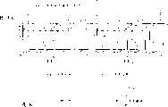
图3A图示耦合到一对存储器通道的存储器控制块的高层框图,其中每个存储器通道包括四个存储器子通道。Figure 3A illustrates a high-level block diagram of a memory control block coupled to a pair of memory channels, where each memory channel includes four memory sub-channels.
图3B图示耦合到高速缓存存储器和一对存储器通道的存储器控制块中的存储器控制器的详细框图,其中每个存储器通道包括多个(S个)子通道。3B illustrates a detailed block diagram of a memory controller in a memory control block coupled to cache memory and a pair of memory channels, where each memory channel includes a plurality (S) of sub-channels.
图4A是图示在使用线性存储器访问而没子通道的情况中将视频显示器上的像素映射到通过存储器通道的存储器访问的示意图。4A is a schematic diagram illustrating the mapping of pixels on a video display to memory accesses through memory channels in the case of using linear memory accesses without sub-channels.
图4B是图示在以两个子通道支持微拼接(micro-tiling)存储器访问的情况中将视频显示器上的像素映射到通过存储器通道的存储器访问的示意图。4B is a schematic diagram illustrating the mapping of pixels on a video display to memory accesses through memory channels in the case of supporting micro-tiling memory accesses with two sub-channels.
图4C是图示在以四个子通道支持微拼接存储器访问的情况中将视频显示器上的像素映射到通过存储器通道的存储器访问的示意图。4C is a schematic diagram illustrating the mapping of pixels on a video display to memory accesses through memory channels in the case of supporting micro-tiled memory accesses with four sub-channels.
图5A是图示通过64位宽的存储器通道的线性64字节存储器访问的示意图。5A is a schematic diagram illustrating linear 64-byte memory access through a 64-bit wide memory channel.
图5B是图示通过一对32位宽的存储器子通道的一对32字节存储器访问的独立子通道存储器访问的示意图。5B is a schematic diagram illustrating an independent sub-channel memory access of a pair of 32-byte memory accesses through a pair of 32-bit wide memory sub-channels.
图5C是图示通过四个16位宽的存储器子通道的四个16字节存储器访问的独立子通道存储器访问的示意图。5C is a schematic diagram illustrating independent sub-channel memory accesses of four 16-byte memory accesses through four 16-bit wide memory sub-channels.
图6图示存储器通道的地址信号线位图。FIG. 6 illustrates an address signal line bitmap of a memory channel.
图7A图示耦合到主机印刷电路板上安装的连接器的多芯片存储器模块的框图。7A illustrates a block diagram of a multi-chip memory module coupled to a connector mounted on a host printed circuit board.
图7B图示主机印刷电路板上嵌入的多个存储器芯片和存储器控制器的框图。Figure 7B illustrates a block diagram of multiple memory chips and a memory controller embedded on a host printed circuit board.
图8图示支持通过存储器子通道的微拼接存储器访问的存储器集成电路的框图。8 illustrates a block diagram of a memory integrated circuit that supports micro-tile memory access through memory sub-channels.
图9A图示用于实现16位宽的存储器子通道和16字节存储器访问的耦合到模式寄存器的地址重载逻辑的示意图。9A illustrates a schematic diagram of address reload logic coupled to a mode register for implementing 16-bit wide memory subchannels and 16-byte memory accesses.
图9B图示用于实现32位宽的存储器子通道和32字节存储器访问的耦合到模式寄存器的地址重载逻辑的示意图。9B illustrates a schematic diagram of address reload logic coupled to a mode register for implementing 32-bit wide memory sub-channels and 32-byte memory accesses.
图9C图示用于实现32位宽的存储器子通道和32字节存储器访问的重排(swizzle)逻辑的示意图。9C illustrates a schematic diagram of swizzle logic for implementing 32-bit wide memory sub-channels and 32-byte memory accesses.
图9D图示用于实现32位宽的存储器子通道和32字节存储器访问而将图9B的地址重载逻辑与图9C的重排逻辑组合的简化逻辑的示意图。9D illustrates a schematic diagram of simplified logic combining the address reload logic of FIG. 9B with the rearrangement logic of FIG. 9C for implementing 32-bit wide memory subchannels and 32 byte memory accesses.
图10图示用于提供微拼接存储器访问的存储器集成电路的方法的流程图。10 illustrates a flow diagram of a method for a memory integrated circuit providing micro-stitched memory access.
附图中相似的引用数字和符号表示指示提供相似功能的单元。Like reference numerals and symbol designations in the figures indicate elements providing similar functions.
具体实施方式Detailed ways
在下文对本发明实施例的详细描述中,给出了许多特定细节以便提供对本发明的透彻理解。但是,对于本领域技术人员来说,显然本发明实施例可以在没有这些特定细节的情况下实施。在其他情况中,对公知的方法、过程、组件和电路未进行详细描述,以不致于妨碍对本发明实施例的多个方面的描述。In the following detailed description of the embodiments of the present invention, numerous specific details are given in order to provide a thorough understanding of the present invention. It will be apparent, however, to one skilled in the art that embodiments of the invention may be practiced without these specific details. In other instances, well-known methods, procedures, components and circuits have not been described in detail so as not to obscure the description of the various aspects of the embodiments of the invention.
由于高速缓存行的大小的原因,集成图形计算机系统的存储器效率通常是有限的。非常常见的情况是,用于图形的理想存储器访问大小是4至16字节的数据,因为图像处理器一次对一个或多个像素或纹素(texel)操作。但是,UMA存储器体系结构是针对64字节高速缓存行来进行优化的,以便优化处理器存储器效率。在64字节高速缓存行的情况中,图形控制器发出的存储器请求平均起来导致大量从存储器提取而从未被图形控制器使用的数据。未使用的数据可以称为过度提取。Integrated graphics computer systems are generally limited in memory efficiency due to the size of cache lines. Very often, the ideal memory access size for graphics is 4 to 16 bytes of data, since image processors operate on one or more pixels or texels at a time. However, the UMA memory architecture is optimized for 64-byte cache lines in order to optimize processor memory efficiency. In the case of a 64-byte cache line, memory requests issued by the graphics controller result in, on average, a large amount of data fetched from memory that is never used by the graphics controller. Unused data can be referred to as over-fetching.
包括微拼接的本发明实施例减少来自图形控制器的存储器请求的过度提取同时维持具有集成图形控制器的UMA存储器体系结构中处理器的高速缓存行需求。通常,微拼接包括新存储器体系结构和新存储器控制器体系结构。虽然描述了新存储器控制器体系结构,但是本申请的焦点在于支持微拼接的新存储器体系结构。为了支持微拼接存储器体系结构,新存储器子系统在存储器通道内提供独立的子通道存储器访问。至存储器中的这些独立的子通道存储器访问可以称为微拼接或微拼接的存储器访问,一般称为微拼接。Embodiments of the present invention that include micro-stitching reduce overfetching of memory requests from a graphics controller while maintaining cache line requirements for processors in a UMA memory architecture with an integrated graphics controller. Typically, micro-stitching includes new memory architectures and new memory controller architectures. Although a new memory controller architecture is described, the focus of this application is a new memory architecture that supports micro-stitching. To support micro-stitched memory architectures, the new memory subsystem provides independent sub-channel memory access within a memory channel. These independent sub-channel memory accesses into memory may be referred to as micro-stitching or micro-stitched memory accesses, generally referred to as micro-stitching.
简言之,微拼接能够实现由对不连续的存储器片段或存储器块的更小请求构成存储器请求。微拼接存储器体系结构能够基于请求方的需求使读和写存储器提取在大小和结构上有所变化。为了正确地标识更小的块,由微拼接的存储器控制器将附加地址信息提供到系统存储器中。例如,在本发明的一个实施例中,可以将64位宽的存储器通道(物理位宽)分成四个16位宽的子通道。在此实现中,64字节存储器访问(存储器通道的逻辑字节宽)由四个不连续的16字节块构成(假定存储器事务是8个传送的突发)。每个子通道使用一些唯一的地址信息。图3A是四个16位子通道的示范实现,其中每个子通道具有一些唯一的地址信息。微拼接存储器体系结构的其他实现可以改变每个子通道的大小以及提供到每个子通道中的独立地址线的数量。In short, micro-tiles enable memory requests to be composed of smaller requests for non-contiguous memory fragments or memory blocks. The micro-tile memory architecture enables read and write memory fetches to vary in size and structure based on the requester's needs. In order to correctly identify the smaller blocks, additional address information is provided into system memory by the micro-tile memory controller. For example, in one embodiment of the present invention, a 64-bit wide memory channel (physical bit width) may be divided into four 16-bit wide sub-channels. In this implementation, a 64-byte memory access (the logical byte width of a memory channel) consists of four non-contiguous 16-byte blocks (assuming a memory transaction is a burst of 8 transfers). Each subchannel uses some unique address information. Figure 3A is an exemplary implementation of four 16-bit sub-channels, where each sub-channel has some unique address information. Other implementations of the micro-tile memory architecture may vary the size of each sub-channel and the number of independent address lines provided into each sub-channel.
有多种方法可用于将附加的独立地址信息提供到存储器阵列的每个子通道,包括通过将新的专用线从存储器控制器布线到存储器集成装置或重新定位(retarget)存储器模块中布线的要作为附加地址线的未用纠错码(ECC)信号线来提供附加地址线。还可以通过在典型未用期间(例如当将列地址写入到存储器集成电路时的存储器周期期间)重载现已存在的地址信号线来提供独立的附加地址信息。在此情况中,可以在存储器模块中实现微拼接支持,并且仍具有对现已存在的存储器模块实现的后向兼容性。这些方法可以单独使用或与本发明实施例组合来使用,以通过期望数量的地址线(包括任何附加地址线)提供附加地址信息。There are various methods that can be used to provide additional independent address information to each sub-channel of the memory array, including by routing new dedicated lines from the memory controller to the memory integrated device or retargeting the routing in the memory module to be used as The unused error correction code (ECC) signal lines of the additional address lines provide additional address lines. Independent additional address information can also be provided by reloading already existing address signal lines during typically unused periods, such as during memory cycles when column addresses are written to the memory integrated circuit. In this case, micro-stitching support can be implemented in a memory module and still have backward compatibility with existing memory module implementations. These methods may be used alone or in combination with embodiments of the present invention to provide additional address information over the desired number of address lines (including any additional address lines).
在本发明的一个实施例中,经主板将附加地址信号线布线到存储器集成电路以支持微拼接和微拼接的存储器访问。这些新的地址信号线是专用的地址线,它们从存储器控制器经主板布线到存储器集成电路装置。在本发明的另一个实施例中,经主板将附加地址信号线布线到新的连接器,并且将具有新引脚分布(pinout)的新存储器模块插入到该新连接器中。In one embodiment of the invention, additional address signal lines are routed to the memory integrated circuit via the motherboard to support micro-stitching and micro-stitching of memory accesses. These new address signal lines are dedicated address lines that are routed from the memory controller through the motherboard to the memory integrated circuit device. In another embodiment of the invention, additional address signal lines are routed through the motherboard to a new connector, and a new memory module with a new pinout is plugged into the new connector.
在本发明的另一个实施例中,可以利用地址信号重载来传送附加地址以支持微拼接。典型的动态随机存取存储器(DRAM)集成电路在行地址选通(RAS#)控制信号断言为低时经这些地址信号线来接收行地址。当列地址选通(CAS#)控制信号断言为低时DRAM集成电路经较少的地址信号线接收列地址。虽然行地址经所有现已存在的地址信号线来发送,但是据观察,常常有较少的列地址经相同的地址信号线发送。即,使用较少的现已存在的地址信号线来传送列地址信号。因此,当CAS#控制信号断言为低时,可以经未用地址信号线将附加地址信号传送到DRAM集成电路。以此方式,只需布设几乎很少的附加地址信号线即可支持微拼接的附加寻址功能。In another embodiment of the present invention, address signal overloading may be utilized to transmit additional addresses to support micro-stitching. A typical dynamic random access memory (DRAM) integrated circuit receives a row address via these address signal lines when a row address strobe (RAS#) control signal is asserted low. A DRAM integrated circuit receives a column address over fewer address signal lines when the column address strobe (CAS#) control signal is asserted low. Although row addresses are sent over all address signal lines that exist, it has been observed that often fewer column addresses are sent over the same address signal lines. That is, column address signals are transmitted using fewer existing address signal lines. Therefore, when the CAS# control signal is asserted low, additional address signals can be sent to the DRAM integrated circuit via the unused address signal lines. In this way, the additional addressing function of micro-stitching can be supported by laying few additional address signal lines.
在本发明的另一个实施例中,可以利用未用纠错码或奇偶检验信号线来传送附加地址以支持微拼接。在一些存储器模块中,可以通过使纠错码(ECC)集成电路监视数据位以及使附加存储器存储ECC数据以支持纠错码(ECC)。但是,通常由于较为昂贵,所以仅在高端系统(例如服务器)中才使用具有ECC的存储器模块。在计算机数量较大的桌上型或客户端计算机中,通常由于ECC是额外的开销而不支持ECC。在这些情况中,通常为ECC或奇偶校验预留的许多存储器模块引脚被闲置未用。在没有ECC的存储器模块中,可以使用未用的ECC或奇偶校验引脚来传送附加地址以支持微拼接。还可以使用其他未用非接触(NC)引脚来提供附加的独立地址信号线以支持微拼接。In another embodiment of the present invention, additional addresses may be transmitted using unused error correction codes or parity check lines to support micro-stitching. In some memory modules, error correction code (ECC) may be supported by having an error correction code (ECC) integrated circuit monitor the data bits and by having additional memory store the ECC data. However, memory modules with ECC are typically only used in high-end systems (eg servers) because they are more expensive. In desktop or client computers with a large number of computers, ECC is usually not supported because ECC is an additional overhead. In these cases, many memory module pins normally reserved for ECC or parity are left unused. In memory modules without ECC, unused ECC or parity pins can be used to communicate additional addresses to support micro-stitching. Other unused non-contact (NC) pins can also be used to provide additional independent address signal lines to support micro-stitching.
在本发明的另一个实施例中,可以通过将未用引脚提供的附加地址信号线与列地址传送期间的地址信号重载组合来实现附加的独立地址信号传送。In another embodiment of the present invention, additional independent address signal transfers can be achieved by combining additional address signal lines provided by unused pins with address signal overloading during column address transfers.
在标准的存储器通道中,例如在基于双数据速率(DDR)DRAM技术的存储器通道中,存储器通道的逻辑宽度可以视为M字节宽。一个数据字节中有8个位。有时存储器通道的逻辑宽度与经存储器模块的数据传送的突发长度相关。即,利用按基地址递增的连续地址,构成一个突发的数据传送连续地访问M字节的数据。通常,要访问(读或写)的字节块的基地址是通道的逻辑宽度的整数倍。存储器通道的物理宽度是存储器控制器与存储器模块之间的数据总线的位宽度。典型的最小突发长度可以是8个存储器周期且起始字节顺序可以由地址线的最低有效位设置。在64位的典型物理宽度的情况中,8个存储器周期访问存储器通道中的64字节的数据。因此,存储器通道的典型逻辑宽度是64字节的数据。In a standard memory channel, such as a memory channel based on Double Data Rate (DDR) DRAM technology, the logical width of the memory channel can be considered Mbytes wide. There are 8 bits in a data byte. Sometimes the logical width of a memory channel is related to the burst length of data transfers through the memory module. That is, a data transfer constituting one burst continuously accesses M bytes of data using consecutive addresses incremented by the base address. Typically, the base address of the block of bytes to be accessed (read or written) is an integer multiple of the logical width of the channel. The physical width of a memory channel is the width in bits of the data bus between the memory controller and the memory modules. A typical minimum burst length may be 8 memory cycles and the starting byte order may be set by the least significant bit of the address line. In the case of a typical physical width of 64 bits, 8
如先前论述的,存储器通道的逻辑宽度是可以利用基地址连续传送的字节数,而存储器通道的物理宽度是存储器控制器与存储器模块之间的数据总线的位宽(“WDB”)。微拼接的存储器系统均等地将存储器通道的逻辑宽度和物理宽度分成具有更小逻辑字节宽度和更小物理位宽度的子通道。As previously discussed, the logical width of a memory channel is the number of bytes that can be transferred contiguously using a base address, while the physical width of a memory channel is the width in bits of the data bus ("WDB ") between the memory controller and the memory modules. A micro-stitched memory system equally divides the logical and physical widths of a memory channel into sub-channels with smaller logical byte widths and smaller physical bit widths.
存储器的微拼接将存储器通道的物理宽度(WDB位)和存储器通道的逻辑宽度(M字节)拆分成S个子通道(WSC)。每个子通道的物理宽度为WSC=WDB/S位而逻辑宽度为N=M/S字节。因此,对于每个数据传送突发,可以经每个子通道中的WSC位的数据线传送N字节的数据。存储器通道可以使存储器中总共有TML个存储器位置供访问。每个子通道访问存储器通道的全部存储器位置(TSML)的一个子集,其中TSML=TML/S。The micro-splicing of the memory splits the physical width (WDB bits) and the logical width (M bytes) of the memory channel into S sub-channels (WSC ). The physical width of each sub-channel is WSC =WDB /S bits and the logical width is N = M/S bytes. Thus, for each data transfer burst, N bytes of data may be transferred over the data lines of the WSC bits in each sub-channel. A memory channel may make a total of TML memory locations in memory available for access. Each sub-channel accesses a subset of the total memory locations (TSML ) of the memory channel, where TSML =TML /S.
在微拼接存储器中,每个子通道可以经存储器通道彼此独立地访问更小粒度的数据。为了使它们完全独立,可以将单独的地址信号线从存储器控制器布线到每个子通道。为了避免布设太多单独的地址信号线,可以在子通道之间共享一些地址信号线,以便可以独立地从一组共用地址中选择存储器位置。因此,呈交到每个子通道的地址具有其值可以不同于呈交给其他子通道的地址中的对应位的多个独立地址位(“I”)。因此,虽然每个子通道上传送的数据表示相邻的数据块,但是每个子通道上的数据块并不一定由来自相邻的地址范围的数据构成。In micro-tile memory, each sub-channel can access smaller-grained data independently of each other through the memory channel. To make them completely independent, separate address signal lines can be routed from the memory controller to each subchannel. To avoid routing too many individual address signal lines, some address signal lines can be shared between subchannels so that memory locations can be independently selected from a common set of addresses. Accordingly, the address presented to each sub-channel has a number of independent address bits ("I") whose values may differ from corresponding bits in addresses presented to other sub-channels. Thus, although the data transferred on each sub-channel represents adjacent blocks of data, the blocks of data on each sub-channel do not necessarily consist of data from adjacent address ranges.
可以在不同的系统中使用本发明的实施例,例如图1A-1B中图示的那些系统。现在参考图1A,其中图示可以利用本发明实施例的典型计算机系统100的框图。计算机系统100A包括第一处理单元101;例如键盘、调制解调器、打印机、外部存储装置等的输入/输出装置(I/O)102;以及例如CRT或图形显示器的监视装置(M)103。监视装置(M)103能以人可理解的格式(例如可视或音频格式)提供计算机信息。系统100可以是除计算机系统外的多种不同电子系统。Embodiments of the present invention may be used in different systems, such as those illustrated in FIGS. 1A-1B . Referring now to FIG. 1A , illustrated therein is a block diagram of a typical computer system 100 in which embodiments of the present invention may be utilized. The
现在参考图1B,其中图示可以利用本发明实施例的客户机服务器系统100B。客户机服务器系统100B包括耦合到网络112的一个或多个客户机110A-110M以及耦合到网络112的服务器114。客户机110A-110M经由网络112与服务器114通信,以便传送或接收信息,并获得对服务器上可能需要的任何数据库和/或应用软件的访问。客户机110A-110M和服务器114可以是典型计算机系统100A的实例。服务器114具有含存储器的处理单元,并且还可以包括一个或多个磁盘驱动器存储装置。服务器114可以在存储区网络(SAN)中用作例如网络连接的存储(NAS)装置,并且具有磁盘阵列。可以由多个客户机110A-110C经网络112共享对服务器114的数据访问。Referring now to FIG. 1B , there is illustrated a
现在参考图2A,其中图示可以利用本发明实施例的第一处理单元101A的框图。处理单元101A可以包括如图所示耦合在一起的处理器电路201、存储器控制块202、外部高速缓存存储器203E、一个或多个存储器通道204A-204N,图形控制器206以及输入/输出控制器207。可以将处理器单元101A的处理器电路201、存储器控制块202、高速缓存存储器203E、图形控制器206和输入/输出控制器207的其中两个或两个以上单元的组合一起集成到单个集成电路中。例如,可以将存储器控制块202、图形控制器206以及输入/输出控制器207一起集成为一个集成电路210。又如,可以将处理器电路201、存储器控制块202、高速缓存存储器203E、图形控制器206以及输入/输出控制器207一起集成为一个集成电路210′。又如,可以将具有其存储器控制器的存储器控制块202集成到处理器电路201中。虽然耦合在处理器电路201与存储器控制块202之间的外部高速缓存存储器203E图示为集成电路210′的一部分,但是它可以是单独的电路。有时,高速缓存存储器203E保留在集成电路210′外部,因为单独制造大存储器容量更有效率。Referring now to FIG. 2A , therein is shown a block diagram of a first processing unit 101A that may utilize embodiments of the present invention. Processing unit 101A may include processor circuitry 201,
处理器电路201可以作为多处理器集成电路包括一个或多个执行单元或多于一个处理器(也称为核处理器),例如处理器A-N201A-201N。处理器电路201的每个处理器可以具有一级或多级芯片上或内部高速缓存存储器203I或共享相同的内部高速缓存存储器。其他多级高速缓存存储器可以在处理器201外部,并与存储器控制器实现接口,例如外部高速缓存存储器203E。与微计算机所具有的那些一样,处理器电路201也可以具有芯片上或内部随机存取存储器(RAM)和芯片上或内部只读存储器(ROM)。处理器201、它的一个或多个执行单元以及一级或多级高速缓存存储器可以经由存储器控制块20连同一个或多个存储器通道204A-204N来读或写数据(包括指令)。The processor circuit 201 may comprise one or more execution units or more than one processor (also referred to as a core processor) as a multiprocessor integrated circuit, such as processors A-N 201A-201N. Each processor of processor circuit 201 may have one or more levels of on-chip or internal cache memory 203I or share the same internal cache memory. Other multi-level cache memories may be external to processor 201 and interface with the memory controller, such as
耦合到一个或多个存储器通道204A-204N和处理器201以及图形控制器206并耦合于它们之间的存储器控制块202可选地具有它自己的内部高速缓存存储器203M或它可以作为另一级高速缓存存储器而为外部的。存储器控制块202包括一个或多个微拼接存储器控制器MCA-MCN 208A-208N,它们各对应于一个或多个存储器通道204A-204N的相应一个The
一个或多个存储器通道204A-204N的每一个包括一个或多个存储器模块MM1-MMn。每个存储器模块包括一个或多个存储器集成电路或装置。所述一个或多个存储器集成电路或装置可以是多种类型的存储器集成电路,包括动态随机存取存储器(DRAM)电路、静态随机存取存储器(SRAM)电路或非易失性随机存取存储器(NVRAM)电路。但是,在本发明的优选实施例中,一个或多个存储器集成电路是动态随机存取存储器(DRAM)电路。Each of the one or
一个或多个存储器通道204A-204N的每一个包括两个或两个以上存储器子通道。在图2A中,在每个存储器通道204A-204N中包含四个存储器子通道205A-205D。暂时参考图2B,在每个存储器通道204A-204N中包含两个存储器子通道205A′-205B′。虽然每个存储器通道中图示了两个和四个子通道,但是应理解还可以有存储器通道的其他划分,包括偶数或奇数个子通道的其他划分。随着存储器通道的逻辑宽度或突发长度增加,此情况尤其突显。Each of the one or
可以将每个存储器通道204A-204N中的一个或多个存储器模块MM1-MMN配置成支持微拼接。存储器控制块可以使用一种算法来确定一个或多个存储器模块是否支持微拼接。可以将一个或多个存储器模块中包含的一个或多个存储器电路或装置配置成支持微拼接。所述一个或多个存储器电路可以是启用微拼接(MTE)的并可以分配所述一个或多个存储器电路来支持特定的存储器子通道。该一个或多个存储器电路可以包括附加的引脚或在模式寄存器中具有用于启用微拼接和分配给特定的存储器子通道的附加位。在由存储器电路提供附加引脚的情况中,可以使用外部跳线引脚、跳线连线或微开关(例如DIP开关)来配置微拼接支持。在存储器电路中提供模式寄存器的情况中,可以使用至每个子通道的数据总线的独立部分来以适合的加载选通加载模式寄存器。One or more memory modules MM1-MMN in each
可以将I/O控制器207耦合到存储器控制块202以便将数据写入所述一个或多个存储器通道204A-204N,这样该数据就可被处理器201访问。处理单元101A还可以包括无线网络接口电路(WNIC)213、有线网络接口电路或网卡(NIC)214、通用串行总线(USB)和/或火线(FW)串行接口215和/或耦合到I/O控制器207的磁盘驱动器216。无线网络接口电路(WNIC)213提供例如经由无线局域联网、wifi(IEEE 802.11)、蓝牙或其他无线电连接的至基本无线电单元的无线电连接。无线联网互连(WNIC)213包括通过无线电波耦合到基本无线电单元或其他移动无线电单元的天线。NIC 214提供以太网连线的局域网连接。USB/FW串行接口215允许扩充系统而包括其他I/O外围设备。磁盘驱动器216是公知的装置,它为处理器201提供可重写存储装置。磁盘存储装置216可以是软磁盘、zip磁盘、DVD光盘、硬盘、可重写光盘、闪速存储器或其他非易失性存储装置的其中一种或多种。An I/
可以将图形控制器206耦合到存储器控制块202以便读取数据和将数据写入到一个或多个存储器通道204A-204N中。处理器201可以将数据写入到一个或多个存储器通道204A-204N,以便该数据可被图形控制器206访问并可在图形显示器或视频装置上显示。可以将图形显示器217耦合到图形控制器206。视频接口218可以耦合到图形控制器206。视频接口218可以是模拟和/或数字的视频接口。
在处理单元101A中,处理器201、I/O控制器207和图形控制器206可以经由存储器控制块202中的存储器控制器来访问一个或多个存储器通道204A-204N中的数据。存储器控制块中的存储器控制器与相应的存储器通道204A-240N实现接口以便在系统存储器与处理器201、I/O控制器207与图形控制器206之间读和写数据。在微拼接的存储器控制器208A-208N分别与存储器通道204A-204N实现接口的情况中,可以有地址总线的地址信号线220、数据总线的数据信号线222和控制与时钟信号线224作为存储器接口的一部分。耦合到I/O控制器207的输入装置(例如磁盘存储装置216)也可以读取信息和将信息写入到系统存储器中。In processing unit 101A, processor 201 , I/
通常,将数据总线的数据信号线222分配给S个子通道。在图2B中,其中S为四,将数据总线的数据信号线222分配到四个子通道,如子通道数据线222A、222B、222C和222D所示,并将它们耦合到相应的子通道205A、205B、205C和205D中。例如,将64位总线划分成四组16位数据线。在本发明的一个实施例中,可以在这些子通道中共享一些地址信号线220中,而其他地址信号线对于子通道彼此独立。在本发明的另一个实施例中,地址信号线220可以在每个子通道中完全是独立的。下文进一步描述地址信号线。Generally, the data signal
现在参考图2B,其中图示可以利用本发明实施例的第二处理单元101B的框图。第二处理单元101B与第一处理单元101A相似,因为它可以包括如图所示耦合在一起的处理器电路201、存储器控制块202、外部高速缓存存储器203E、一个或多个存储器通道204A-204N,图形控制器206以及输入/输出控制器207。为了简化,对于相似编号的单元请参考图2A的描述,在此不进行赘述。但是在第二处理单元101B中,如图所示,将一个或多个存储器通道204A-204N的每个存储器通道分配到两个子通道205A′和205B′中。即,子通道的数量S为2。如图所示,通过子通道数据线222A和222B将数据总线的数据信号线222分配到两个子通道,并将这些数据信号线222耦合到相应的子通道205A′和205B′。例如,将64位总线划分成两组32位数据线。在本发明的一个实施例中,可以在这些子通道的每个子通道中共享一些地址信号线220中,而其他地址信号线对于子通道彼此独立。在本发明的另一个实施例中,地址信号线220可以在每个子通道中完全是独立的。Referring now to FIG. 2B , therein is illustrated a block diagram of a
现在参考图3A,其中图示两个存储器通道的框图。图3A图示组合的图形与存储器控制器300,也称为主机300,它耦合到存储器通道0 304A和存储器通道1 304B。分别将存储器通道0 304A和存储器通道1 304B划分成四个子通道305A、305B、305C和305D。每个存储器通道具有独立的微拼接存储器控制器以支持存储器通道的子通道。每个存储器通道具有独立的数据总线。例如,假定存储器通道的每个数据总线为总共64位数据位宽,则每个子通道耦合到一组独立的16位的数据总线。将子通道305 A耦合到数据位D15-D0,将子通道305B耦合到数据位D31-D16,将子通道305C耦合到D47-D32,以及将子通道305D耦合到数据位D63-D48,如图3A中所示。Referring now to FIG. 3A, therein is shown a block diagram of two memory channels. FIG. 3A illustrates a combined graphics and
如前文论述的,在本发明的一个实施例中,可以在这些子通道的每个子通道中共享一些地址信号线中,而其他地址信号线对于子通道彼此独立。例如,地址信号线310(标记为Axx-A10、BA2-BA0)对于所有子通道305A-305D都是共享的。即,这些地址信号线310的每个地址信号线都可以向外发散,并耦合到每个子通道。相比之下,地址信号线311A(标记为A9-A6的第一组)独立地耦合到子通道305A。地址信号线311B(标记为A9-A6的第二组)独立地耦合到子通道305B。地址信号线311C(标记为A9-A6的第三组)独立地耦合到子通道305C。地址信号线311D(标记为A9-A6的第四组)独立地耦合到子通道305D。As previously discussed, in one embodiment of the present invention, some of the address signal lines may be shared among each of the sub-channels, while other address signal lines are independent of each other for the sub-channels. For example, address signal lines 310 (labeled Axx-A10, BA2-BA0) are shared by all sub-channels 305A-305D. That is, each address signal line of these
理想的情况下,提供足够的独立地址线能够实现分配的存储器页大小粒度内的完全可寻址。通常由管理图形存储器空间的软件来设置页大小。例如,考虑两个通道高速缓存行交织的存储器子系统中进行4千字节(KB)页大小分配的情况。将2KB的页映射到每个存储器通道。在此情况中,可以使用五个地址线来寻址存储器的每个物理页中的32个64B高速缓存行。因此,十五个附加的独立地址线对于四个16位子通道的实现应是理想的。它们图示为最初第一组地址信号线311A、标记为第一组地址线A10-A6,其下是地址信号线311B-D,分别标记为第二组、第三组和第四组地址线(标为A10-A6)。如果将较少的附加独立地址线设为可用,则每个子通道可寻址的独立地址空间减少。如果将更多独立地址线设为可用于每个子通道,则增加每个子通道可寻址的独立地址空间。为了实现两个32位子通道,期望具有五个附加独立地址线。Ideally, providing enough independent address lines enables full addressability within the granularity of the allocated memory page size. The page size is usually set by the software that manages the graphics memory space. For example, consider the case of a 4 kilobyte (KB) page size allocation in a memory subsystem with two-way cache-line interleaving. A 2KB page is mapped to each memory channel. In this case, 32 64B cache lines in each physical page of memory can be addressed using five address lines. Therefore, fifteen additional independent address lines should be ideal for four 16-bit sub-channel implementations. They are shown initially as the first group of
在本发明的一个实施例中,可以在存储器控制器与子通道之间布设额外的地址信号线,以便提供独立地址信号线,如图3A所示。在本发明的另一个实施例中,可以将地址信号重载到现已存在的地址线上。在本发明的另一个实施例中,可以采用布设额外地址信号线与重载地址信号的组合来支持微拼接。在本发明的另一个实施例中,可以为每个子通道提供一组完整的独立地址线,而无需图3A所示的共享的地址线310。但是,使用共享的地址信号线310因避免独立地址信号线的布线而省下了印刷电路板区域。In one embodiment of the present invention, additional address signal lines can be laid between the memory controller and the sub-channels to provide independent address signal lines, as shown in FIG. 3A . In another embodiment of the invention, address signals can be overridden onto existing address lines. In another embodiment of the present invention, a combination of routing additional address signal lines and reloading address signals may be used to support micro-splicing. In another embodiment of the present invention, a complete set of independent address lines may be provided for each sub-channel without the shared
暂时参考图6,其中图示使用共享的地址位和独立地址位的存储器通道的地址信号线位图。即,图6是图示地址位在物理地址中的解释的地址位图。将一组I个独立地址位(IAB)提供到每个子通道以支持微拼接。可以将一组零个或多个(SA个)共享的地址位(SAB)提供到所有的子通道。将存储器请求分配到子通道时使用一组Q个子通道选择位(SSB)。在DRAM存储器内,使用一组P个子通道数据地址位(SDAB)来寻址DRAM存储器内每个高速缓存行中的字节。该组P个SDAB位通常是地址信号线图(line map)的最低有效位。实际上在存储器控制器与子通道存储器之间并未路由该组Q个SSB位和P个SDAB位,应理解,正在访问的数据块的基地址是突发大小的整数倍。即,可以由存储器集成电路、例如DRAM装置根据双数据速率(DDR)存储器规范在内部生成P个SDAB位。虽然图6图示了选择来共享的某些地址位和独立地址位,但是可以分配其他地址位。即,将P个子通道数据地址(SDAB)位上的地址位划分成SA个共享的地址(SAB)位和I个独立地址(IAB)位一般是任意的。Referring momentarily to FIG. 6, there is illustrated an address signal line bitmap for a memory channel using shared address bits and individual address bits. That is, FIG. 6 is an address bit map illustrating the interpretation of address bits in a physical address. A set of 1 independent address bits (IAB) is provided to each sub-lane to support micro-stitching. A set of zero or more (SA) shared address bits (SAB) may be provided to all sub-channels. A set of Q sub-channel select bits (SSBs) are used to allocate memory requests to sub-channels. Within DRAM memory, a set of P sub-channel data address bits (SDAB) are used to address bytes in each cache line within DRAM memory. The set of P SDAB bits is typically the least significant bits of the address signal line map. The set of Q SSB bits and P SDAB bits is not actually routed between the memory controller and the sub-channel memory, it being understood that the base address of the data block being accessed is an integer multiple of the burst size. That is, the P SDAB bits may be generated internally by a memory integrated circuit, such as a DRAM device, according to the Double Data Rate (DDR) memory specification. While FIG. 6 illustrates certain address bits selected to be shared and individual address bits, other address bits may be assigned. That is, the division of the address bits on the P sub-channel data address (SDAB) bits into SA shared address (SAB) bits and I independent address (IAB) bits is generally arbitrary.
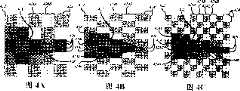
现在参考图4A-4C,图示使用拼接的地址空间对三角形的理想化像素图渲染。图4A图示使用非微拼接的存储器系统在拼接的地址空间中对三角形401的光栅化,在该非微拼接的存储器系统中逻辑通道宽度是64字节。图4B-4C图示使用微拼接的存储器系统在拼接的地址空间中对三角形401的光栅化。三角形401的光栅化的单位是片元(fragment)402。一个片元402可以表示一个像素或纹素。拼接的地址空间是一种其中将逻辑上二维的数据阵列组织为一组子阵列以使子阵列内的数据存储在连续的地址空间范围中并因此在存储器中高度局部化的地址空间。线性寻址的逻辑上二维的数据阵列没有这种子阵列;相反而是在行中从左到右、然后从上到下下移到下一行来线性地寻址例如片元402的数据。因此,垂直方向上相邻的片元402在存储器中可能相距较远。Referring now to FIGS. 4A-4C , there are illustrated idealized pixmap renderings of triangles using a tiled address space. Figure 4A illustrates the rasterization of a
与图4A比较,图4B-4C示出微拼接存储器访问如何提供更小的存储器请求的优点。图4A-4C的每一个附图示出对应于不同存储器请求大小的三角形401的光栅化。Compared to Figure 4A, Figures 4B-4C illustrate how micro-stitched memory accesses provide the advantage of smaller memory requests. Each of Figures 4A-4C shows the rasterization of a
在图4A中,单个存储器请求包含表示16个片元的数据。这些个体方块402的每一个方块表示一个片元,每个片元通常为32位或4字节的数据。图4A-4C图示20×20片元的阵列。如图4A所示,4×4片元的阵列是跨度(span)404,表示64字节存储器请求。图4C中将子跨度424图示为2×2片元的阵列或16字节存储器请求。图4B中图示双子跨度414,它是按2×4片元的阵列朝向的32字节存储器请求。In Figure 4A, a single memory request contains data representing 16 fragments. Each of these
图4A-4C之间的差异说明了因为存储器请求大小减小在过度提取中的理论上减小。在图4A-4C的每一个附图中,三角形401需要访问相同数量的片元。但是,存储器访问通常传送多于一个片元的数据,从而它可能包含表示三角形401内的片元408和三角形401外的片元406的数据。表示三角形401外的片元406的数据是过度提取的,这导致无效率地利用存储器宽度。The difference between Figures 4A-4C illustrates the theoretical reduction in overfetching due to the reduction in memory request size. In each of Figures 4A-4C,
在图4A中,64字节存储器访问传送跨度404的数据,4×4片元块。例如,跨度404A是第一个64字节存储器访问。跨度404B是第二个64字节存储器访问。例如,考虑三角形401包含大约57个像素要渲染。对于64字节存储器访问的情况,需要10个存储器访问来访问该三角形内的65个片元。额外95个片元的数据被访问,但是可能不会被使用。In FIG. 4A, a 64-byte memory access transfers data that spans 404, a 4x4 tile block. For example, span 404A is the first 64-byte memory access.
在图4B中,32字节存储器访问传送双子跨度的数据,2×4片元块或64字节存储器访问的一半。例如,双子跨度414A是第一个32字节存储器访问。双子跨度414B是第二个32字节存储器访问。对于32字节存储器访问的情况,需要13个存储器访问来访问该三角形内的65个片元。额外47个片元的数据被访问,但是可能不会被使用。In FIG. 4B, a 32-byte memory access transfers a double sub-span of data, a 2x4 slice block or half of a 64-byte memory access. For example,
在图4C中,16字节存储器访问传送子跨度的数据,2×2片元块或64字节存储器访问的四分之一。跨度424A是第一个16字节存储器访问。跨度424B是第二个16字节存储器访问。跨度424C是第三个16字节存储器访问。跨度424D是第四个16字节存储器访问。对于16字节存储器访问的情况,需要22个存储器访问来访问该三角形内的65个片元。额外13个片元的数据被访问,但是可能不会被使用。In FIG. 4C, a 16-byte memory access transfers a subspan of data, a 2x2 slice block, or one quarter of a 64-byte memory access.
考虑另一个示例,在图4A、4B和4C的每一个中三角形401需要65个像素或片元(260字节)来显示。在图4A中,大约存储器的10个跨度被访问,包括160个像素或640字节数据来渲染三角形401。在图4B中,大约13个双子跨度数据被访问,包括112个像素或448字节的数据来渲染三角形401。在图4C中,大约22个子跨度的数据被访问,包括88个片元或352字节的数据来渲染三角形401。因此与图4A相比,图4B和4C中利用在每个存储器通道内的子通道实现微拼接寻址减少了过度提取的像素或片元406。Consider another example, in each of Figures 4A, 4B and
如前文所论述的,图4B-4C图示使用包括存储器子通道的微拼接的存储器系统在拼接的地址空间中对三角形401的光栅化。在图4B中,可以由两个32字节宽的存储器子通道构成64字节宽的存储器通道。在此情况中,微拼接的存储器访问将两个不相邻的32字节访问组合成一个64字节访问,对两个子通道的每个子通道各执行一个访问,总共64字节的大小。对三角形的光栅化产生访问双子跨度414的请求。例如,微拼接存储器控制器可以将访问双子跨度414C和414D的请求组合成单个微拼接的存储器访问。又如,该存储器控制器可以将访问双子跨度414E和414F的请求组合成单个微拼接的存储器请求。可以将访问双子跨度的请求的其他组合构成单个微拼接的存储器请求或访问。在本发明的一个或多个实施例中,组合的子通道访问具有SA个共享的地址位中的共享的地址位模式。As previously discussed, FIGS. 4B-4C illustrate the rasterization of a
在图4C中,可以由四个16字节宽的存储器子通道构成64字节宽的存储器通道。在此情况中,微拼接的存储器访问将四个不相邻的16字节访问组合成单个64字节访问,对四个子通道的每个子通道各执行一个访问,总共64字节的大小。对三角形的光栅化产生访问子跨度424的请求。例如,微拼接存储器控制器可以将访问子跨度424E、424F、424G和424H的请求组合成单个微拼接的存储器访问。可以将访问子跨度的请求的其他组合构成单个微拼接的存储器请求或访问。在本发明的一个或多个实施例中,组合的子通道存储器访问对应于四个存储器子通道的每一个存储器子通道具有SA个共享的地址位中的共享的地址位模式。In FIG. 4C, a 64-byte wide memory channel may be formed from four 16-byte wide memory sub-channels. In this case, the micro-stitched memory access combines four non-contiguous 16-byte accesses into a single 64-byte access, one for each of the four sub-lanes, for a total size of 64 bytes. Rasterization of a triangle generates a request to access
在理想的情况中,假定所有微拼接的存储器请求都可以被微拼接事务汇编器利用来构建64B存储器事务而没有未使用的子通道。即,微拼接的效率取决于事务汇编器326A、326B构造充分填充的存储器事务的能力。In an ideal case, it is assumed that all micro-tile memory requests can be utilized by the micro-tile transaction assembler to construct a 64B memory transaction with no unused subchannels. That is, the efficiency of micro-stitching depends on the ability of the
现在参考图3B,其中图示多通道存储器子系统,该多通道存储器子系统包括耦合到系统存储器通道的微拼接的存储器控制块300和一个或多个高速缓存存储器203。在存储器控制块300内,多通道存储器子系统包括用于至系统存储器的每个存储器通道的微拼接存储器控制器。Referring now to FIG. 3B , there is illustrated a multi-channel memory subsystem comprising a micro-tile
在图3B中,提供两个存储器通道304A和304B。因此,为相应的存储器通道304A和304B提供两个微拼接存储器控制器321A和321B。每个存储器通道304A、304B可以由S个子通道305A-305S组成。每个子通道305在逻辑上为N字节宽和B位宽。每个存储器通道304在逻辑上为M=N*S字节宽。In FIG. 3B, two
在存储器控制块300与高速缓存存储器203之间的是写数据路径301和读数据路径302,它们可以包括其上可发出读和写请求的命令路径或地址路径。在读事务的情况中,从存储器控制块300经读数据路径302将N字节返回到高速缓存203。在写事务的情况中,从高速缓存203经写数据路径301将N字节写请求提供到存储器控制块300。虽然在高速缓存203与存储器控制块300之间发出N字节读或写请求,但是将请求描述为2×2拼接阵列以表示2×2像素或纹素阵列,例如可在四个子通道的情况中使用的。Between
存储器控制块300包括通道分配器320、第一存储器控制器321A以及第二存储器控制器321B。存储器控制块300还耦合到存储器通道0 304A和存储器通道1 304B。存储器通道0 304A包括“S”个子通道305A-305S。相似地,存储器通道1 304B包括“S”个子通道305A-305S。共享的地址线310从每个存储器控制器322耦合到每个子通道305A-305S。独立地址线311A-311S耦合到相应的子通道305A-305S。数据总线子通道部分312A-312S的每个部分耦合到相应的存储器子通道305A-305S。The
存储器控制器321A包括子通道分配器322A、重排序缓冲器324A和事务汇编器326A并且存储器控制器321B包括子通道分配器322B、重排序缓冲器324B和事务汇编器326B。
将N字节数据的存储器请求、通道的逻辑宽度耦合到通道分配器320中。通道分配器将存储器请求分配到存储器通道0 304A或存储器通道1 304B,具体根据包括存储器通道的易变性(variability)的情况而定。在由通道分配器分配到存储器通道之后,将N字节请求耦合到相应的存储器控制器321A或321B中以及耦合到子通道分配器322A或322B中。A memory request of N bytes of data, the logical width of the lane, is coupled into
子通道分配器322A和322B将N字节请求分配到子通道305A-305S的其中之一。暂时参考图6,可以通过如下过程定义标识子通道分配s:(1)将请求地址“A”右移位P SDAB位,得到新的整数值


微拼接存储器控制器321A-321B的每一个微拼接存储器控制器分别具有重排序缓冲器324A和重排序缓冲器324B。重排序缓冲器将存储器请求重新排序到子通道中,以便增加每个存储器通道中的带宽效率。要在地址“A”处读或写N字节数据块的请求进入存储器控制器322A或322B,并被分配到子通道,然后被置于重排序缓冲器中。重排序缓冲器可以作为每个子通道的重排序队列来实现。重排序缓冲器的其他实现也是可能的。Each of the
事务汇编器326A、326B通过从重排序缓冲器中选择S个读请求(每个子通道一个)来形成读事务,使得所有S个请求具有相同的共享的地址位。通过从重排序缓冲器中选择S个写请求(每个子通道一个)来形成写事务,使得所有S个请求具有相同的共享的地址位。例如,事务汇编器326A、326B可以每个子通道对应于一个地在存储器通道中由四个16字节请求汇编一个64字节事务。The
当尝试形成事务时,微拼接的控制器中的事务汇编器可能无法找到一组并行的请求(每个子通道一个),使得SA个共享的地址位对于所有子通道是相同的。在这种情况中,可以不在未找到请求的子通道上传送任何数据,或如果在该子通道上传送数据,则可以废弃该数据。When trying to form a transaction, the transaction assembler in the micro-tile's controller may not be able to find a parallel set of requests (one for each sublane) such that the SA shared address bits are the same for all sublanes. In this case, no data may be transmitted on the sub-channel for which the request was not found, or if data was transmitted on the sub-channel, the data may be discarded.
现在参考图5A-5C,其中图示对应于每个存储器通道500A-500C的示范字节排序。在图5A中,存储器通道500A具有从0到63编号的64字节的传送大小。可以由64位物理宽度的存储器通道访问64字节的逻辑宽度。Referring now to FIGS. 5A-5C , there are illustrated exemplary byte orderings corresponding to each memory channel 500A- 500C. In FIG. 5A, memory channel 500A has a transfer size of 64 bytes numbered from 0-63. A logical width of 64 bytes can be accessed by a memory channel of a physical width of 64 bits.
在图5B中,可以将存储器通道500B划分成两个存储器子通道505A和505B,每个存储器子通道传送64字节传送的一半,从而每个子通道传送32字节。对于存储器子通道505A来说,对图5A所示的进行了重新排序,被访问的存储器字节编号为从0到31。对于存储器子通道505B来说,对图5A所示的进行了重新排序,被访问的字节编号为从32到63。In FIG. 5B, memory channel 500B may be divided into two memory sub-channels 505A and 505B, with each memory sub-channel transferring half of a 64-byte transfer such that each sub-channel transfers 32 bytes. For memory sub-channel 505A, the sequence shown in FIG. 5A is reordered, and the accessed memory bytes are numbered from 0 to 31 . For memory subchannel 505B, reordered from that shown in FIG. 5A, the bytes accessed are numbered from 32 to 63.
在图5C中,可以将存储器通道500C划分成四个存储器子通道515A、505B、515C和515D,每个存储器子通道传送64字节传送的四分之一,从而每个子通道传送16字节。存储器子通道515A访问对图5A所示的重新排序的编号为从0到15的存储器字节。存储器子通道515B访问对图5A所示的重新排序的存储器字节16到31。存储器子通道515C访问对图5A所示的重新排序的编号为32-47的字节。存储器子通道515D访问对图5A所示的重新排序的编号为48-63的字节。以此方式,将64字节传送均等地分布在这些存储器子通道的每个存储器子通道之间,同时对字节编号重新排序和分配。In FIG. 5C, memory channel 500C may be divided into four memory sub-channels 515A, 505B, 515C, and 515D, with each memory sub-channel transferring a quarter of a 64-byte transfer, whereby each sub-channel transfers 16 bytes. Memory subchannel 515A accesses memory bytes numbered from 0 to 15 for the reordering shown in FIG. 5A . Memory subchannel 515B accesses the reordered memory bytes 16 through 31 shown in FIG. 5A . Memory subchannel 515C accesses bytes numbered 32-47 for the reordering shown in FIG. 5A. Memory subchannel 515D accesses bytes numbered 48-63 for the reordering shown in FIG. 5A. In this way, the 64-byte transfers are evenly distributed among each of the memory sub-channels, while byte numbers are reordered and distributed.
现在参考图6,在本发明的其他实施例中,可以采用不同方式对字节重新排序。Referring now to FIG. 6, in other embodiments of the present invention, the bytes may be reordered in different ways.
如先前论述的,为了支持微拼接存储器访问,可以使用SA个共享的地址位以及I个独立地址位,同时利用Q个子通道选择位和P个子通道数据地址位来寻址高速缓存行访问的物理字节。对于64字节高速缓存行来说,Q个子通道选择位和P个子通道数据地址位之和是6。As previously discussed, to support micro-stitched memory accesses, SA shared address bits and I individual address bits can be used while utilizing Q sub-channel select bits and P sub-channel data address bits to address the physical cache line access byte. The sum of Q sub-channel select bits and P sub-channel data address bits is six for a 64-byte cache line.
在图6中,将P个子通道数据地址位指示为A0-A8。在图6中,Q个子通道选择位标记为A10、A8以及如果还有其他子通道选择位则标记为A10与A8之间的编号。在图6中,I个独立地址位标记为A9、A10、A16、A18、A24以及如果还有其他独立地址位则标记为A9、A10、A16、A18、A24之间的编号。在图6中,SA个共享的地址位标记为例如A11、A15、A17、A19、A20、A25、A26和Ax。在这些编号之间的编号可以用于另外的共享的地址位。In FIG. 6, the P sub-channel data address bits are indicated as A0-A8. In FIG. 6, the Q sub-channel selection bits are labeled A10, A8 and, if there are other sub-channel selection bits, the numbers between A10 and A8. In FIG. 6, one independent address bit is marked as A9, A10, A16, A18, A24 and if there are other independent address bits, it is marked as a number between A9, A10, A16, A18, A24. In FIG. 6, the SA shared address bits are labeled, for example, A11, A15, A17, A19, A20, A25, A26, and Ax. Numbers between these numbers can be used for additional shared address bits.
就I个独立地址位而言,子通道地址在彼此的地址偏移量内是独立的。为了使子通道完全彼此独立,可以使用将命令和地址完整地从存储器控制器复制到每个子通道,但是这会大大地增加存储器控制器引脚计数,输入/输出驱动器的硅区域以及主机印刷电路板或主板上所需的布线区域。相反,本发明的实施例在所有子通道之间共享一个或多个部分的子通道地址位,并允许余下I个独立地址位对于每个子通道是独立的,如图6所示。因此,妥当地选择I个独立地址位可以实现平衡I个地址信号复制到每个子通道的成本的前提下的带宽效率的提高。The sub-channel addresses are independent within an address offset of each other in terms of 1 independent address bit. To make the subchannels completely independent of each other, a complete copy of the commands and addresses from the memory controller to each subchannel could be used, but this would greatly increase the memory controller pin count, the silicon area of the input/output drivers, and the host printed circuit required routing area on the board or motherboard. In contrast, embodiments of the present invention share one or more portions of subchannel address bits among all subchannels, and allow the remaining 1 independent address bits to be independent for each subchannel, as shown in FIG. 6 . Therefore, properly selecting one independent address bit can realize the improvement of bandwidth efficiency under the premise of balancing the cost of copying one address signal to each sub-channel.
如先前所论述的,能以不同方式获取I个独立地址位,包括将附加的地址线布线到每个存储器子通道和/或使用地址重载。As previously discussed, the 1 independent address bit can be obtained in different ways, including routing additional address lines to each memory sub-channel and/or using address reloading.
现在参考图7A,其中图示存储器模块(MM)710,它是存储器模块MM1-MMn的示范。存储器模块710可以是任何类型的存储器模块,例如SIMM或DIMM。存储器模块710包括耦合到印刷电路板751的存储器集成电路芯片(“存储器装置”)752。印刷电路板751包括耦合到主机印刷电路板762的边缘连接器760的边缘连接器或边缘连接754。Referring now to FIG. 7A, there is shown a memory module (MM) 710, which is exemplary of memory modules MM1-MMn.
为了支持存储器的微拼接,在本发明的一个实施例中,可以使用印刷电路板751的边缘连接754的引脚分布的未用或未连接引脚来将附加的地址信号线独立地提供到存储器集成电路752。可以使用边缘连接754的这些未用或未连接引脚将附加的独立地址信号线布线到存储器集成电路752。在装配到主板762的对应边缘连接器760中可见到相同的未用引脚。在主板762上将附加的独立地址信号线763从存储器控制块中的存储器控制器布线到现已存在的连接器,以提供附加的独立地址信息。可以发现存储器模块的边缘连接754的引脚分布有许多不同类型的未用或未连接引脚。To support micro-stitching of memory, in one embodiment of the present invention, additional address signal lines may be independently provided to the memory using unused or unconnected pins of the pinout of
例如,奇偶校验或纠错码(ECC)功能可以具有作为边缘连接754的引脚分布的一部分预留的引脚。为了将存储器模决的成本降低到消费级,常常从存储器模块取消奇偶校验和ECC功能,而使预留的信号线和引脚常常被闲置未用。即,奇偶校验/ECC信号线可能布线到主板的所有边缘连接器中,但是仅当其中安装了启用ECC的存储器模块(例如双列直插存储器模块(DIMM))时,这些奇偶校验/ECC信号线才会被使用。将存储器模块的现已存在的未用ECC线/引脚重新定位为独立地址信号线,并用于实现非ECC存储器模块中的微拼接。但是,在使用ECC线/引脚来实现微拼接时,无法在存储器模块上同时启用ECC和微拼接功能。此解决方案在通常不需要(或不想要)启用奇偶校验/ECC的环境中较为有效。For example, a parity check or error correction code (ECC) function may have pins reserved as part of the
又如,边缘连接754的引脚分布中预留的可选低有效(active low)数据信号线常常闲置未用,因为它们作为所提供的高有效(active high)信号线的备用。又如,存储器模块的边缘连接754的引脚分布内预留的可选测试引脚常常闲置未用,因为未使用该测试模式。As another example, the optional active low data signal lines reserved in the pinout of the
在任何情况中,将这些未用引脚重新定位以作为独立地址信号引脚755A-755D,以及在主机印刷电路板762上布设独立地址信号线763,在存储器模块710的PCB 751上将独立地址信号线756A-756D布线到存储器集成电路752。In any event, these unused pins are relocated as individual address signal pins 755A-755D, and individual
在一些情况中,存储器模块710还可以包括支持集成电路750,例如缓冲器集成电路(“缓冲器”)或纠错控制(ECC)集成电路。但是如先前论述的,如果存储器模块710上不提供ECC,则可以将为ECC预留且未用的边缘连接754引脚用于至存储器子通道的独立地址线来支持微拼接。In some cases,
为了支持微拼接和存储器子通道的独立寻址,可以将存储器模块710上的存储器集成电路752划分并分配到不同的存储器子通道,例如图7A所示的四个存储器子通道205A、205B、205C和205D。存储器集成电路752的数据I/O通常为4、8或16位宽。对于存储器通道的物理宽度为64位以及每个存储器子通道为16位的情况,将四个16位宽的存储器集成电路752分别一对一地分配到四个存储器子通道205A、205B、205C和205D。将八个8位宽的存储器集成电路752分别一次两个地分配到四个存储器子通道205A、205B、205C和205D来为存储器通道提供64位的物理宽度并为每个存储器子通道提供16位。将十六个4位宽的存储器集成电路752分别一次四个地分配给四个存储器子通道205A、205B、205C和205D来为存储器通道提供64位的物理宽度并为每个存储器子通道提供16位。In order to support micro-stitching and independent addressing of memory sub-channels, the memory integrated
在两个存储器子通道的情况中,将四个16位宽的存储器集成电路752分别一次两个地分配到两个存储器子通道来为存储器通道提供64位的物理宽度以及为每个存储器子通道提供32位。将八个8位宽的存储器集成电路752分别一次四个地分配给两个存储器子通道来为存储器通道提供64位的物理宽度并为每个存储器子通道提供32位。将十六个4位宽的存储器集成电路752分别一次八个地分配给两个存储器子通道来为存储器通道提供64位的物理宽度并为每个存储器子通道提供32位。In the case of two memory subchannels, the four 16-bit wide memory integrated
利用存储器模块的边缘连接754的未用引脚和标准边缘连接器760,存储器模块710可以与现已存在的存储器子系统后向兼容。在本发明的另一个实施例中,为新的边缘连接754和新的边缘连接器760提供添加的独立地址信号线以支持微拼接存储器。但是在本发明的此实施例中,专门将存储器模块和边缘连接器设计为支持存储器的微拼接而不与现已存在的系统后向兼容。在本发明的另一个实施例中,存储器集成电路焊接到主板,而非使用存储器模块710或边缘连接器760。Utilizing the unused pins of the memory module's
现在参考图7B,通过直接焊接到主机印刷电路板762来将752存储器集成电路752连同具有微拼接的存储器控制器208A-208N的存储器控制块202以及其他组件一起嵌入到主机印刷电路板762上,这些组件的其中一些是先前在图2A-2B中描述和图示的。以主机印刷电路板762上的布线区域为代价,可以在存储器控制块202中的微拼接的存储器控制器208A-208N与存储器集成电路752之间布设独立地址信号线766A-776D。在不同的存储器子通道205A-205D中的存储器集成电路752之间不共享这些独立地址信号线766A-776D。但是可以在相同存储器子通道中的一个或多个存储器集成电路752中间共享这些独立地址信号线。Referring now to FIG. 7B , the memory integrated
例如考虑图3A,其中每个存储器通道中可见到四个独立存储器子通道。可以对每个子通道提供附加的四个独立地址线以独立地访问每个子通道中的存储器区域。地址线311A-311D(标记为A9-A6)在每个子通道内是独立的。给定现已存在一组四个地址线,要布设的附加地址线的总数是3乘以4即12个独立地址信号线。当将存储器焊接在主板上时布设附加的信号线较为有效。或者,当现已存在的边缘连接器和存储器模块的引脚分布未被完全利用时,可以利用在主板上将附加的信号线布线到存储器模块来添加独立的地址信令。但是,如果现已存在的接头的引脚被完全利用时,则没有用于附加线的空间,该方法或布设附加信号线则不是容易实现的,尤其是在要求后向兼容性的情况下。Consider, for example, Figure 3A, where four independent memory sub-channels are visible in each memory channel. An additional four independent address lines may be provided for each sub-channel to independently access memory regions in each sub-channel.
现在参考图8,其中图示存储器集成电路800的框图。存储器集成电路800作为一个或多个存储器装置752包括在存储器模块MM1-MMn中。存储器集成电路800包括如图示耦合在一起的存储器阵列801、行地址解码器802、位线预充电/刷新逻辑803、列解码器804、传感放大器阵列和写驱动器块806、控制器808、地址缓冲器811和微拼接控制逻辑812。微拼接控制逻辑812还可以称为重载逻辑(OL)。Referring now to FIG. 8 , therein is shown a block diagram of a memory integrated
控制器808包括模式寄存器810,模式寄存器810具有可以经设置/初始化来控制存储器集成电路800的一般功能的许多位。模式寄存器包括用于存储位的位存储电路。可以通过将适合的位设置值应用于与加载选通相符的地址线820或数据线821来设置模式寄存器810的位。可以在存储器处于空闲时,通过开关一个或多个控制线822来生成加载选通,其中一个或多个控制线822被耦合到存储器集成电路的控制器808。控制器808接收一个或多个控制线822。一个或多个控制线822可以包括行地址选通RAS#、列地址选通CAS#、写使能WE#、芯片组CS#、存储器组选择BA0、BA1、BA2或其他标准存储器集成控制输入。The
更确切地来说,模式寄存器810可以用于配置集成电路800来实现微拼接存储器访问。正如下文进一步论述的,模式寄存器810的一个或多个位是微拼接使能位。微拼接使能位可以是高有效,并称为MTE位。或者,微拼接使能位可以是低有效,并称为MTE#。在这两种情况的任一种情况中,微拼接使能位一般可以称为微拼接使能位或MTE位。缺省情况下将微拼接使能位复位,使得装置最初加电或复位时禁用微拼接。这使得存储器模块710和存储器集成电路800在插入到不支持微拼接的系统中时能后向兼容。模式寄存器810还具有一个或多个子通道选择(SCS)位,它们指示存储器集成电路所分配的且存储器集成电路可访问的存储器子通道。将MTE位和一个或多个SCS位耦合到微拼接控制逻辑812中。More specifically,
微拼接控制逻辑812耦合到多个地址信号线820,以便经由地址缓冲器811将地址耦合到列地址解码器804和/或行地址解码器802。地址缓冲器811可以锁存内部地址信号线上的地址信号以便为地址解码器保存它们。控制逻辑812还耦合到控制器的模式寄存器来接收微拼接使能位和至少一个子通道选择位,以便支持对存储器阵列801的微拼接存储器访问。响应微拼接使能位和至少一个子通道选择位,控制逻辑812选择要从其上为其所分配的预定子通道捕获独立地址信息的一个或多个地址信号线。即,仅可以将地址信号线的一个子集分配到预定的子通道。控制逻辑812选择该子集的地址信号线来提取独立地址信息。可以将其他地址信号线用于其他子通道或一些地址信号线是每个子通道中共享的地址信号线。控制逻辑812将独立地址信息耦合到列地址解码器804和/或行地址解码器802。通过控制逻辑选择一个或多个地址信号线还可以响应列地址加载信号(CAS#)和事务使能信号来进行。
可以将附加的控制逻辑添加到微拼接控制逻辑812中以及添加到其周围,以便进一步重排一个有效位到另一个有效位位置的独立地址信息。当启用微拼接时,这某种程度地提供了线性寻址方法,例如用于屏幕刷新的线性寻址方法。Additional control logic may be added in and around the
传感放大阵列和写驱动器块806耦合到数据输入/输出(I/O)总线,并且可以从控制器808接收控制信号以从存储器阵列801读取数据或将数据写入到存储器阵列801。传感放大阵列和写驱动器块806接收要写入到存储器阵列801的数据,并将从存储器阵列801读取的数据驱动到数据输入/输出(I/O)总线821上。数据输入/输出(I/O)总线821包括存储器集成电路800的双向数据线,这些双向数据线通常为4、8或16位宽。Sense amplifier array and write
存储器阵列801由可以按行和列组织的存储器单元组成。存储器单元通常是动态随机存取存储器(DRAM)单元,但是作为可选项也可以是静态类型的随机存取存储器(SRAM)单元或非易失性可编程(NVRAM)类型的可重写存储器单元。
行地址解码器802在地址线上接收行地址,并在字线(WL)之一上生成信号,以便寻址存储器阵列801中的一行存储器单元。列解码器804也在地址线上接收列地址,并选择要寻址该行存储器单元内的哪些列。列解码器804实质上选择至要访问的存储器单元的位线。在读访问中,列解码器804起复用器的作用。在写访问中,列解码器804起解复用器的功能。列地址解码器804响应共享的列地址信号选择性地访问存储器阵列801内的存储器单元的列,如果模式寄存器内的微拼接使能位被设置,则列地址解码器804响应独立子通道列地址信号选择性地访问存储器阵列801内的存储器单元的列。
传感放大器阵列和写驱动器块406可以包括传感放大器,传感放大器用于确定读操作期间在被访问的存储器单元内存储了逻辑1还是逻辑0。读操作期间,被寻址的存储器单元尝试将逻辑1或逻辑0驱动到存储器阵列的所选位线上。在读操作期间,传感放大器检测被寻址的存储器单元将逻辑1还是逻辑0驱动到存储器阵列的所选位线上。传感放大器阵列和写驱动器块406还可以包括写驱动器,写驱动器用于在写操作期间将逻辑1或逻辑0驱动到存储器阵列的所选位线上,以及驱动到被寻址的存储器单元中。The sense amplifier array and write
预充电/刷新块803耦合到存储器阵列801中的位线。在读或写操作期间,预充电/刷新块803可以在寻址存储器单元之前预处理位线。预充电/刷新块803还可以在不活动期间刷新存储器阵列801的存储器单元中存储的数据。Precharge/
在特定的存储器周期期间,至存储器集成电路800的一些现存信号线未被使用,因此可以在此期间将它们重新定位用于其他目的。例如,在CAS(列地址选通)周期期间,并非所有地址线都被使用。可以在CAS周期期间将这些未用的数据信号线重新定位,来将附加地址信息传送到存储器模块(例如DIMM)和其中的存储器集成电路装置。在CAS周期期间,存储器控制块202中的存储器控制器208在这些未用地址信号线上发送附加地址信息。具有添加的微拼接控制逻辑电路812的存储器集成电路800和模式寄存器810内的位识别CAS周期期间未被使用的先前未用地址信号线上的这些重载的信号并将其解码。During a particular memory cycle, some existing signal lines to the memory integrated
现在参考图9A,其中图示为了支持微拼接,示范微拼接存储器控制逻辑812A耦合到存储器集成电路内的模式寄存器810A。微拼接存储器控制逻辑812A的示范实现将含有未用存储器周期(例如CAS周期)期间提供的附加地址信息的重载的地址信号线解码。微拼接存储器控制逻辑812A的示意图假定提供四个子通道,其中每个子通道具有用于支持微拼接的16字节的逻辑宽度。Referring now to FIG. 9A , there is shown an exemplary micro-stitching
微拼接存储器控制逻辑812A的中央是双路4输入复用器900,该双路4输入复用器900用于捕获独立地址信息。微拼接存储器控制逻辑812A的双路4输入复用器900选择性地在复用的输出(A3′和A4′)上输出共享的列地址信号或独立子通道列地址信号。双路4输入复用器的输出(A3′和A4′)耦合到列地址解码器的输入。独立子通道列地址信号是已选择要被相应存储器子通道接收的一个或多个独立列地址信号。Central to the micro-stitch
微拼接控制逻辑812A从存储器集成电路的地址引脚接收地址线。微拼接控制逻辑812A将地址提供到地址缓冲器,以便将其分发到行地址解码器和列地址解码器。存储器集成电路的一些地址引脚接收共享的行地址信号、共享的列地址信号、独立列地址信号或它们的组合。例如,地址引脚A5-A9和A13绕过到微拼接控制逻辑812A,并可以将共享的行地址信号和/或共享的列地址信号接收到每个存储器子通道中。地址引脚A0-A4和A10-A12耦合到双路4输入复用器900,并且如果启用微拼接,则可以接收共享的行地址信号和独立列地址信号。如果未启用微拼接,则耦合到双路4输入复用器900的地址引脚A3和A4可以接收共享的行地址信号和/或共享的列地址信号。列地址加载选通引脚CAS#耦合到控制逻辑812A以接收列地址加载选通信号并在分配到给定子通道用于存储器集成电路内捕获的地址引脚上选择性地接收适合的一个或多个独立列地址信号。还可以使用列地址加载选通信号来从适合的地址引脚接收和捕获共享的列地址信号。
模式寄存器810A可以包括3位存储电路、例如触发器或存储器单元,用于存储微拼接使能(MTE)位、子通道选择位0(SCS0)位和子通道选择位1(SCS1)位的设置值。模式寄存器810A中的这三位是利用适合的子通道选择位和微拼接使能位来编程的。在初始化(例如加电或复位)期间,这三位被设置/根据存储器集成电路接收的位设置值复位。这三位还可以在存储器集成电路空闲且没有存储器访问正在进行时被设置/复位。可以在地址或数据信号线上接收位设置值,并响应耦合到存储器集成电路中的一个或多个控制线输入生成的加载选通信号而将其加载到模式寄存器中。如果要在存储器集成电路中启用微拼接,则微拼接使位MTE被设置。因为MTE位是高有效,所以将其设为高逻辑电平。如果是低有效,则将MTE#位设为逻辑低电平。在图9A的示范控制逻辑中,存储器通道内可能有四个或四个以下的子通道。SCS0和SCS1位将存储器集成电路分配到四个存储器子通道的其中之一。可以将相同存储器模块上的其他存储器集成电路分配到四个存储器子通道中的另一个存储器子通道。The
在CAS周期期间,使每个子通道的独立地址信息可存在于现已存在的地址线(例如地址线A0-A4和A10-A12)上。在此示例中,一般使用地址线A3和A4。因此,地址线A0、A1、A2、A10、A11、A12和A13是重载的信号线(A13可以是微拼接事务启用的-基于事务指定的)。在现已存在的地址线上重载信号线的此方法将实际上六个附加地址线(A0-A2和A10-A12)提供到存储器集成电路装置,而不使用附加的线路(即线路布线)或不使用附加的引脚。During the CAS cycle, independent address information for each sub-channel is made available on existing address lines (eg, address lines A0-A4 and A10-A12). In this example, address lines A3 and A4 are generally used. Therefore, address lines A0, A1, A2, A10, A11, A12, and A13 are reloaded signal lines (A13 may be micro-stitched transaction enabled - based on transaction assignment). This method of overloading the signal lines on the already existing address lines provides effectively six additional address lines (A0-A2 and A10-A12) to the memory integrated circuit device without using additional wiring (i.e., wire routing) or without using the additional pins.
每个存储器集成电路中提供微拼接存储器控制逻辑812A,以便响应模式寄存器中存储的子通道选择位从地址线A0-A4和A10-A12中选择适合的独立子通道地址信息。将子通道选择位的设置值从模式寄存器810A路由到微拼接存储器控制逻辑812A以控制复用器900的输入选择过程。复用器900的输出端耦合到地址信号线A3′和A4′。地址信号线A3′和A4′耦合到地址解码器(例如列地址解码器804)以选择存储器阵列内的存储器单元。Micro-stitched
微拼接控制逻辑可以在列地址写访问时间期间且CAS#是低有效(“CAS周期”)时重载存储器地址信号线A3′和A4′。即,在没有微拼接的情况下,当正在将列地址写入到存储器集成电路时,地址位A0、A1、A2、A10、A11和A12通常是未被使用的地址位。被A3′和A4′代替的地址位A3和A4是用于将列地址写入到存储器集成电路的地址位。虽然CAS周期期间在没有微拼接的情况下地址位一般未被使用,但是在RAS#为低有效(“RAS周期”)时且将行地址写入到存储器集成电路中时,可以使用它们来选择存储器集成电路中的行地址。这在本文称为地址重载。虽然在图9A中将A0、A1、A2、A10、A11和A12图示为在列地址选通CAS#期间未用的地址位,但是可以利用不同的未用地址位作为重载的地址信号线来支持微拼接。The micro-tile control logic may reload memory address signal lines A3' and A4' during column address write access times and when CAS# is active low ("CAS cycle"). That is, without micro-stitching, address bits A0, A1, A2, A10, A11, and A12 are typically unused address bits when the column address is being written to the memory integrated circuit. Address bits A3 and A4 replaced by A3' and A4' are address bits for writing a column address to the memory integrated circuit. Although the address bits are generally unused during a CAS cycle without micro-stitching, they can be used to select the A row address in a memory integrated circuit. This is referred to herein as address overloading. Although A0, A1, A2, A10, A11, and A12 are illustrated in FIG. 9A as unused address bits during column address strobe CAS#, different unused address bits can be utilized as reloaded address signal lines. to support micro-splicing.
微拼接存储器控制逻辑812A包括如图示耦合在一起的双路4输入复用器900、3输入AND门电路903、多个2输入AND门电路904-911以及多个反相器912-918。众所周知,AND门电路可以由NAND门电路与将其耦合到NAND门电路的输出的反相器的组合来形成。The micro-tile
双路4输入复用器900是一对4至1复用器,其中每个4至1复用器具有耦合在一起的第一选择控制输入S0和耦合在一起的第二选择控制输入S1。第一4至1复用器接收输入1I0-1I3,并响应选择控制输入S0和S1来提供输出1Y。第二4至1复用器接收输入2I0-2I3,并响应选择控制输入S0和S1来提供输出2Y。如果S0和S1都是逻辑低或0,则输入1I0和2I0被复用到相应的输出1Y和2Y上。如果S0是逻辑高或1而S1是逻辑低或0,则输入1I1和2I1被复用到相应的输出1Y和2Y上。如果S0是逻辑低或0而S1是逻辑高或1,则输入1I2和2I2被复用到相应的输出1Y和2Y上。如果S0和S1都是逻辑高或1,则输入1I3和2I3被复用到相应的输出1Y和2Y上。Dual 4-
双路4输入复用器900的第一4输入复用器在其相应的输入1I0-113处接收地址位A3、A0、A1和A2,并选择它们的其中之一以在其1Y输出处驱动到地址信号线A3′上。第二4输入复用器在其相应的2I0-2I3输入处接收地址位A4和A10-A12,并选择它们的其中之一在其2Y输出处驱动到地址信号线A4′上。选择控制输入S0和S1分别耦合到AND门电路904-905的输出。The first 4-input multiplexer of dual 4-
AND门电路903在其输出处生成微拼接模式信号(MTM)902A。微拼接模式信号902A是高有效,并在独立地址信号在耦合到双路4输入复用器900的重载的地址信号线上时的适合时间生成。反相器912在其耦合到AND门电路903的输入的输出处将低有效CAS#信号取反成高有效CAS信号。AND门电路903将CAS信号、MTE位设置值(ME)和事务使能信号(TE、地址位A13)进行逻辑与运算以生成微拼接模式信号902 A。即如果MTE位启用微拼接,且TE信号启用事务,则在CAS#变为低时,生成微拼接模式信号(MTM)902A。AND gate 903 generates micro-tile mode signal (MTM) 902A at its output. The
微拼接模式信号(MTM)902A被耦合到AND门电路904和905的输入来门控(gate)子通道选择位SCS0和SCS1。如果出于任何原因,微拼接模式信号(MTM)902A为低,则进入复用器900的选择控制S0和S1在AND门电路904和905的输出处逻辑上为低或0。在S0和S1为逻辑低或0的情况下,分别耦合到输入1I0和2I0的地址位A3和A4分别在相应的输出1Y和2Y处复用到地址信号线A3′和A4′上。位A3和A4仅分别通过信号线A3′和A4′。如果未启用微拼接或如果处于任何其他目的使用位A3和A4(例如行寻址),则这是缺省条件。Micro Tile Mode signal (MTM) 902A is coupled to the inputs of AND
当微拼接模式信号(MTM)902A是高有效时,子通道选择位SCS0和SCS1分别通过AND门电路904和905分别耦合到复用器900的选择控制输入S0和S1。因此,当由AND门电路903将微拼接模式信号(MTM)902A生成为高有效时,子通道选择位SCS0和SCS1控制将复用器900的相应四个输入复用到相应输出的选择。指示可以将存储器IC分配到的子通道的子通道选择位SCS0和SCS1的设置值实际上确定在CAS周期期间使用耦合到复用器900的哪些地址位线来捕获独立地址信号。When micro tiling mode signal (MTM) 902A is active high, subchannel select bits SCS0 and SCS1 are coupled to select control inputs S0 and S1 of
子通道选择位SCS0和SCS1的设置值将对于不同子通道而不同。对于四个子通道,分别有四个不同SCS0和SCS1的设置值。但是注意可以仅使用两个不同的子通道选择位SCS0和SCS1的不同设置值容易地将设计为支持四个子通道的微拼接控制逻辑缩减为支持两个子通道。利用SCS0和SCS1的不同设置值,在生成微拼接模式信号时,复用器900选择不同的地址信号线来捕获独立地址信号。The setting values of the sub-channel selection bits SCS0 and SCS1 will be different for different sub-channels. For the four sub-channels, there are four different setting values of SCS0 and SCS1 respectively. Note however that a micro-splice control logic designed to support four sub-channels can be easily reduced to support two sub-channels using only two different setting values of the sub-channel select bits SCS0 and SCS1. Using different setting values of SCS0 and SCS1 , when generating micro-splice mode signals, the
微拼接模式信号(MTM)902A还分别在至AND门电路906-911的第一输入处耦合到反相器913-918。地址信号A0、A1、A2、A10、A11和A12分别耦合到AND门电路906-911的第二输入。微拼接模式信号(MTM)902A实际上门控分别在AND门电路906-911的输出A0′、A1′、A2′、A10′、A11′和A12′处进入存储器集成电路的地址线A0、A1、A2、A10、A11和A12上的信号。即,当微拼接模式信号(MTM)902A逻辑上为低或0时,AND门电路906-911允许地址线A0、A1、A2、A10、A11和A12上的信号通过而到达输出A0′、A1′、A2′、A10′、A11′和A12′上并到达地址解码器。当微拼接模式信号(MTM)902A在逻辑上为高或1时,AND门电路906-911驱动所有输出A0′、A1′、A2′、A10′、A11′和A12′为逻辑低或0。因此,当微拼接模式信号(MTM)902A为高有效来捕获独立地址信息时,不使用输出A0′、A1′、A2′、A10′、A11′和A12′,因为它们全部被驱动为0。Micro Tile Mode signal (MTM) 902A is also coupled to inverters 913-918 at first inputs to AND gates 906-911, respectively. Address signals A0, A1, A2, A10, A11 and A12 are coupled to second inputs of AND gates 906-911, respectively. Micro Tile Mode signal (MTM) 902A actually gates address lines A0, A1, Signals on A2, A10, A11 and A12. That is, AND gates 906-911 allow signals on address lines A0, A1, A2, A10, A11, and A12 to pass to outputs A0', A1 when micro-tile mode signal (MTM) 902A is logically low or 0. ', A2', A10', A11' and A12' and reach the address decoder. AND gates 906-911 drive all outputs A0', A1', A2', A10', A11' and A12' to logic low or 0 when micro-tile mode signal (MTM) 902A is logic high or 1. Thus, outputs A0', A1', A2', A10', A11', and A12' are not used because they are all driven to zero when micro-tile mode signal (MTM) 902A is active high to capture independent address information.
现在参考图9B,其中图示为了支持微拼接,模式寄存器810B耦合到存储器集成电路内的微拼接控制逻辑812B。微拼接控制逻辑812B在功能上某种程度地与微拼接控制逻辑812A相似,只是微拼接控制逻辑812B用于使用低有效控制信令并支持存储器通道内的两个子通道。微拼接控制逻辑812B中的电路被构成减少通过复用器的选择控制输入来选择地址信号线上的独立地址信号时的延迟。在要支持两个存储器子通道的情况下,微拼接控制逻辑812B接收选为从中接收的地址信号线上的两组独立地址信号。微拼接存储器控制逻辑812B的中央是六路2输入复用器901A,该六路2输入复用器901A用于从地址信号线捕获独立地址信息。微拼接控制逻辑812B中的六路2输入复用器901A接收更多且不同的地址信号线,在这些地址信号线上可以选择性地接收多组独立地址信号。即,图6所示的I个独立地址位的数量更大。因此,存储器子通道内的可独立访问的存储器空间更大。Referring now to FIG. 9B , there is shown a
微拼接控制逻辑812B耦合到存储器集成电路的地址引脚,包括地址引脚A0-A8和A10-A13。在CAS周期期间使每个子通道的独立地址信息可存在于这些现已存在的地址线上。微拼接控制逻辑选择性地在内部地址信号线A3′-A8′上形成独立子通道地址信号。内部地址信号线A0′-A8′和A11′-A13′经由地址缓冲器耦合到地址解码器。地址缓冲器可以响应RAS#和CAS#选通信号来锁存内部地址信号线A0′-A8′和A11′-A13′上的地址信号,然后将这些地址信号耦合到地址解码器。如图所示,地址引脚A0-A8和A10-A13在未用存储器周期期间已重载地址信号,并耦合到六路2输入复用器901A的输入。地址信号线A3-A8是第一组地址信号线,可以经第一组地址信号线将第一组独立地址信号耦合到第一存储器子通道中。地址信号线A0-A2和A11-A13是第二组地址信号线,可以经第二组地址信号线将第二组独立地址信号耦合到第二存储器子通道中。响应第一子通道选择位(SCS0)和微拼接模式信号(MTM#)902B,微拼接控制逻辑812B一般在接收用于第一存储器子通道的第一组独立地址信号或用于第二存储器子通道的第二组独立地址信号之间选择。在六路2输入复用器901A的输出处提供所选的一组独立地址信号。这些独立地址信号耦合到存储器集成电路中以便独立地寻址可以耦合到每个存储器子通道中的SA个共享的地址位所构成的一组共用存储器位置内的不同存储器位置。
在CAS周期期间,使每个子通道的独立地址信息可存在于现已存在的地址线(例如地址线A0-A4和A10-A12)。在此示例中,一般使用地址线A3-A8。因此,地址线A0-A2和A10-A12是重载的信号线(A13可以是微拼接事务启用的-基于事务指定的)。在现已存在的地址线上重载信号线的此方法将六个附加地址线(A0-A2和A10-A12)实际上提供到存储器集成电路装置,而不使用附加的线路(即线路布线)或不使用附加的引脚。During a CAS cycle, independent address information for each sub-channel is made available on existing address lines (eg, address lines A0-A4 and A10-A12). In this example, address lines A3-A8 are generally used. Therefore, address lines A0-A2 and A10-A12 are reloaded signal lines (A13 may be micro-stitched transaction enabled-based on transaction assignment). This method of overloading the signal lines on the already existing address lines effectively provides six additional address lines (A0-A2 and A10-A12) to the memory integrated circuit device without using additional wiring (i.e., wire routing) or without using the additional pins.
模式寄存器810B可以包括2位存储电路、例如触发器或存储器单元,它用于存储低有效微拼接使能位MTE#和子通道选择位0(SCS0)的设置值。模式寄存器接收这两个位的位设置值。使用一个或多个控制信号生成的加载选通信号将这两个位设置值加载到模式寄存器中。在初始化(例如加电或复位)期间,这三位被设置/根据存储器集成电路接收的位设置值复位。在存储器集成电路空闲且没有存储器访问正在进行时这三位也会被设置/复位。可以在地址或数据信号线上接收位设置值,并响应耦合到存储器集成电路中的一个或多个控制线输入生成的加载选通信号来将其加载到模式寄存器中。The
模式寄存器810A中的MTE#位和SCS0位是利用适合的子通道选择位和微拼接使能位来编程的。如果要在存储器集成电路中启用微拼接,则将微拼接使能位(MTE#)低有效信号设为逻辑低电平。当存储器子系统支持微拼接时,微拼接使能位被设置。否则,不设置微拼接使能位,使得存储器集成电路与不支持微拼接的较旧系统后向兼容。在图9B的示范控制逻辑中,存储器通道内可能有两个可能的子通道。SCS0位将存储器集成电路分配到存储器通道内的两个存储器子通道的其中一个。可以将相同存储器模块上的其他存储器集成电路分配到另一个存储器子通道。The MTE# and SCS0 bits in the
每个存储器集成电路中提供微拼接存储器控制逻辑812B,以便响应模式寄存器中存储的子通道选择位从地址信号引脚中选择适合的独立子通道地址信息。将子通道选择位的设置值从模式寄存器路由到微拼接存储器控制逻辑以控制复用器901A的输入选择过程。Micro-stitched
微拼接控制逻辑812B包括如图9B所示耦合在一起的第一六路2输入复用器901A、第二六路2输入复用器901B、多个AND门电路906-911、多个反相器913-918和3输入OR门电路923。众所周知,可以通过将反相器的输入耦合到NOR门电路的输出来构成OR门电路。先前已提供AND门电路的公知构成方式。The
第一六路2输入复用器901A的输出耦合到第二六路2输入复用器901B中的每个复用器的两个输入的第一个输入。地址位或信号线A3、A4、A5、A6、A7和A8耦合到第二六路2输入复用器901B中的每个复用器的两个输入的第二个输入。第二六路2输入复用器901B的输出端耦合到地址信号线A3′-A8′。地址信号线A3′和A8′耦合到地址解码器(例如列地址解码器804)来选择存储器阵列内的存储器单元。地址缓冲器可以锁存或寄存地址信号线A3′-A8′以保存其状态,以便地址解码器可以将它们解码。The output of the first six-way 2-input multiplexer 901A is coupled to the first of the two inputs of each multiplexer in the second six-way 2-input multiplexer 901B. Address bits or signal lines A3, A4, A5, A6, A7 and A8 are coupled to the second of the two inputs of each of the second six 2-input multiplexers 901B. The output of the second six-way 2-input multiplexer 901B is coupled to address signal lines A3'-A8'. Address signal lines A3' and A8' are coupled to an address decoder (eg, column address decoder 804) to select memory cells within the memory array. The address buffer can latch or register the address signal lines A3'-A8' to preserve their state so that the address decoder can decode them.
第一六路2输入复用器901A使其选择控制S0耦合到子通道选择0(SCS0)位,使得直接通过存储器集成电路的子通道分配来控制复用器901A的输出。以此方式,较好地处理所选的输出以将地址信号的传播延迟降至最小。第二六路2输入复用器901B使其选择控制输入S0耦合到3输入OR门电路923的输出、低有效微拼接模式(MTM#)信号902B。如果低有效微拼接模式(MTM#)信号902B逻辑上为低或0,则启用微拼接存储器访问,使得第一六路2输入复用器901A的输出是第二六路2输入复用器901B在地址信号线A3′-A8′上的相应逻辑输出。如果未启用微拼接访问,则MTM#为高,由此选择第二六路2输入复用器901B中的每个复用器的两个输入的第二个输入,并将地址信号线A3-A8耦合到独立子通道列地址线A3′-A8′上。在此情况中,第一六路2输入复用器901A对地址信号A3-A8没有任何影响,这实际上使地址信号A3-A8绕过微拼接控制逻辑812B并分别驱动到内部地址线A3′-A8′上。The first six-way 2-input multiplexer 901A has its select control SO coupled to the subchannel select 0 (SCSO) bit so that the output of the multiplexer 901A is controlled directly by the subchannel assignment of the memory integrated circuit. In this way, the selected outputs are better processed to minimize the propagation delay of the address signals. A second six-way 2-input multiplexer 901B has its select control input SO coupled to the output of a 3-input OR
六路2输入复用器901A-901B是将选择控制输入S0耦合在一起的六个2至1复用器。第一2至1复用器接收输入1I0和1I1,并响应选择控制输入S0来提供输出1Y。第二2至1复用器接收输入2I0和2I1,并响应选择控制输入S0来提供输出2Y。第三2至1复用器接收输入3I0和3I1,并响应选择控制输入S0来提供输出3Y。第四2至1复用器接收输入4I0和4I1,并响应选择控制输入S0来提供输出4Y。第五2至1复用器接收输入5I0和5I1,并响应选择控制输入S0来提供输出5Y。第六2至1复用器接收输入6I0和6I1,并响应选择控制输入S0来提供输出6Y。如果S0为逻辑低或0,则分别将输入1I0、2I0、3I0、4I0、5I0和6I0驱动到输出1Y、2Y、3Y、4Y、5Y和6Y上。如果S0为逻辑高或1,则分别将输入1I1、2I1、3I1、4I1、5I1和6I1驱动到输出1Y、2Y、3Y、4Y、5Y和6Y上。Six 2-input multiplexers 901A-901B are six 2-to-1 multiplexers that couple select control input S0 together. A first 2 to 1 multiplexer receives inputs 1I0 and 1I1 and provides an
如先前论述的,3输入OR门电路923在其输出处生成低有效微拼接模式(MTM#)信号902B。在其输入处,3输入OR门电路923接收微拼接使能位MTE#、列地址选通CAS#信号以及事务使能位TE#(地址线A10)。如果所有这3个输入为低逻辑电平或0,则微拼接模式(MTM#)信号902B在逻辑上为低或0,以便从重载的地址线选择性地接收独立子通道地址信号。这要求通过将微拼接使能位设为它的低有效电平或0来启用微拼接;通过将地址线A10设为逻辑低或0来启用微拼接事务;以及通过将CAS#控制信号选通为逻辑低或0来将列地址选通到存储器集成电路。即,所有这些输入信号为低有效进入控制逻辑812B来实现微拼接存储器访问。如果输入MTE#、CAS#或TE#的任何其中之一是逻辑高或1,则微拼接模式(MTM#)信号902B在逻辑上为高或1。在微拼接模式(MTM#)信号902B在逻辑上为高或1的情况下,控制逻辑812B的第二六路2输入复用器901B按常规将地址信号A3-A8传递到内部地址线A3′-A8′,而不选择任何独立子通道地址信号信息。要求多于一个信号来启用微拼接访问可确保不会因仅一个位信号中的错误而误进入微拼接模式。As previously discussed, the 3-input OR
控制逻辑812B中的AND门电路906-911以与控制逻辑812A中的AND门电路906-911相似的方式工作,只是控制逻辑812B中的AND门电路906-911选通不同的地址信号,并且可以在没有反相器913-918的情况下执行此操作,因为微拼接模式(MTM#)信号902B是低有效的信号。因此,控制逻辑812B中的AND门电路906-911响应微拼接模式(MTM#)信号902B为低有效而分别在内部地址线A0′-A2′和A11′-A12′上将地址信号A0-A2和A11-A12门控为0。AND gates 906-911 in
现在参考图9C,其中图示地址重排逻辑930的示意图,地址重排逻辑930耦合到模式寄存器810C。图9C所示的地址重排逻辑930是用于具有两个存储器子通道的存储器通道的。可以在图9A和9B所示的重载或微拼接控制逻辑812A或812B之前或之后加设重排控制逻辑。Referring now to FIG. 9C , therein is shown a schematic diagram of
简言之,提供地址重排逻辑930以便利用微拼接的存储控制器实现某种程度的线性寻址能力,例如屏幕刷新期间可能需要的线性寻址能力。地址重排逻辑930选择性地将从存储器控制器接收到的地址位的有效位重新排序或转置。实现此操作的一种方式是交换位的位置。可以实现此操作的另一种方式是选择性地将地址位反相。Briefly, address
地址重排逻辑930包括如图所示耦合在一起的双路2输入复用器935、NOR门电路936和异或(XOR)门电路)937-938。双路2输入复用器935包括其选择控制输入S0耦合在一起并耦合到从NOR门电路936输出的重排控制信号(SWZ)932的一对2输入复用器。地址位或引脚A4和A3分别耦合到复用器935的110和210输入,当选择控制输入S0在逻辑上为低或0时选择地址位或引脚A4和A3来输出。XOR门电路937-938的输出分别耦合到复用器935的1I1和2I1输入,当选择控制输入S0在逻辑上为高或1时选择XOR门电路937-938的输出来输出。
子通道选择位1(SCS1)和子通道选择位0(SCS0)分别地耦合到异或(XOR)门电路937-938的第一输入。地址位A3和A4分别耦合到XOR门电路937和938的第二输入。如果SCS1位设为1,则XOR门电路937在其输出处将地址位A3取反,其中其输出耦合到复用器935的1I1。如果SCS0位被设为1,则XOR门电路938在其输出处将地址位A4取反,其中其输出耦合到复用器935的2I1。以此方式,SCS1和SCS0位的设置值实际上可以将地址位线A3和A4上的地址信号反相。Sub-channel select bit 1 (SCS1) and sub-channel select bit 0 (SCS0) are coupled to first inputs of exclusive OR (XOR) gates 937-938, respectively. Address bits A3 and A4 are coupled to second inputs of
NOR门电路936在其输出处生成重排控制信号(SWZ)932,其中其输出耦合到双路2输入复用器935的选择控制输入S0。重排控制信号(SWZ)932、高有效信号选择重排的地址位是否被选择从双路2输入复用器935输出。如果重排控制信号(SWZ)932在逻辑上为高或1且耦合到双路2输入复用器935的选择控制输入S0,则选择从XOR门电路937和938输出的重排的地址位以便驱动到复用器935的输出处的相应的地址线A4″和A3″上。如果通过低有效微拼接使能位MTE#启用微拼接,CAS#选通信号在逻辑上为低以捕获列地址信息,并且TE#位在逻辑上为低以启用微拼接事务,这三个信号都输入到NOR门电路936中,则会出现此情况。但是,如果重排控制信号(SWZ)932在逻辑上为低或0,耦合到双路2输入复用器935的选择控制输入S0,则地址位A4和A3在复用器935的输出处通过相应的地址线A4″和A3″而不重排。如果未通过低有效微拼接使能位MTE#启用微拼接,或如果CAS#选通信号在逻辑上不为低以捕获列地址信息,或如果TE#位在逻辑上不为低以启用微拼接事务,则会出现此情况。NOR
模式寄存器810C与模式寄存器810B相似,只是模式寄存器810C存储附加位(SCS1)的设置值。模式寄存器810C可以包括3位存储电路、例如触发器或存储器单元,用于存储低有效的微拼接使能(MTE)位、子通道选择位0(SCS0)位和子通道选择位1(SCS1)位的设置值。该模式寄存器接收这些位的位设置值。使用一个或多个控制信号生成的加载选通信号将这些位设置值加载到模式寄存器中。在初始化(例如加电或复位)期间,这三位被设置/根据存储器集成电路接收的位设置值复位。这三位还可以在存储器集成电路空闲且没有存储器访问正在进行时被设置/复位。可以在地址或数据信号线上接收其位设置值,并响应耦合到存储器集成电路的一个或多个控制线输入生成的加载选通信号来将其加载到模式寄存器中。
因为将地址信号延迟保持得尽可能小是重要的,所以可以将图9B的地址重排逻辑与图9C所示的重载逻辑组合并进行简化来减少内部地址信号线上的信号延迟。Because it is important to keep address signal delays as small as possible, the address rearrangement logic of FIG. 9B can be combined and simplified with the reload logic shown in FIG. 9C to reduce signal delays on the internal address signal lines.
现在参考图9D,其中图示将重排和微拼接控制逻辑950耦合到存储器集成电路中的模式寄存器810C。控制逻辑950将图9C的地址重排逻辑930与图9B的重载或微拼接控制逻辑812B组合并进行简化。因此,组合的重排和微拼接控制逻辑950起到与微拼接控制逻辑812B和地址重排逻辑930的单独组件相似的作用。在控制逻辑950中进行简化的目的是要缩减存储器集成电路中至地址解码器和地址缓冲器的地址信号路径的时间延迟。该对六路2输入复用器901A和901B已简化成单个六路3输入复用器960。Referring now to FIG. 9D , there is illustrated coupling of rearrangement and
如先前描述的,模式寄存器810C包括低有效微拼接使能位(MTE#)、SCS0位和SCS1位。可以利用耦合到存储器集成电路的控制信号生成的加载选通从位设置值加载模式寄存器位。As previously described, the
控制逻辑950包括如图所示耦合在一起的六路3输入复用器960、AND门电路906-910、OR门电路923、AND门电路969、异非或(XNOR)门电路974-975和反相器976。或者异非或(XNOR)门电路974-975可以是SCS0和SCS1的位设置值被取反的异或(XOR)门电路。控制逻辑950耦合到地址引脚A0-A8和A10-A13接收地址信号,并在地址信号线A0′-A8′和A10′-A13′上生成内部地址信令。地址信号输入A10执行作为微拼接模式中的事务使能位TE#和作为地址输入信号的双重任务。
在控制逻辑中,可以首先将始于地址引脚的地址信号线耦合到地址重排逻辑,然后才将其耦合到六路3输入复用器960。例如,将地址A4耦合到XNOR门电路974的输入,将地址A1耦合到XNOR门电路975,以及将地址A0耦合到反相器976。如果SCS0位设置为逻辑低或0,则XNOR门电路974-975将相应的地址信号A4和A1取反,然后才将其分别耦合到复用器960的1I0和1I1输入。如果SCS0位设置为逻辑高或1,则XNOR门电路974-975传递相应的地址信号A4和A1而不取反,然后才将其分别耦合到复用器960的1I0和1I1输入。In the control logic, the address signal lines from the address pins may be coupled first to the address rearrangement logic and only then to the six-way 3-
六路3输入复用器960是六个3至1复用器,其具有耦合在一起的第一选择控制输入S0和耦合在一起的第二选择控制输入S1。第一3至1复用器接收输入1I0、1I1和1I2,并响应选择控制输入S0和S1来提供输出1Y。第二3至1复用器接收输入2I0、2I1和2I2,并响应选择控制输入S0和S1来提供输出2Y。第三3至1复用器接收输入3I0、3I1和3I2,并响应选择控制输入S0和S1来提供输出3Y。第四3至1复用器接收输入4I0、4I1和4I2,并响应选择控制输入S0和S1来提供输出4Y。第五3至1复用器接收输入5I0、5I1和5I2,并响应选择控制输入S0和S1来提供输出5Y。第六3至1复用器接收输入6I0、6I1和6I2,并响应选择控制输入S0和S1来提供输出6Y。Six 3-
六路3输入复用器960具有第一选择控制输入S0和第二选择控制输入S1,用于选择要将三个输入的哪个输入耦合到相应的输出。因为利用两个选择控制输入来进行四选一是可能的,所以现在将描述六路3输入复用器的真值表。如果选择位S0和S1都设为0,则选择I0输入来从复用器输出。如果S0位设为1且S1位设为0,则选择I1输入来从复用器输出。如果S1位设为1,则不考虑S0的位设置值而选择I2输入来从复用器输出。即,在此情况中,当S1位设为1时不考虑输入到六路3输入复用器中的S0,因为是覆盖(overriding)。The six-way 3-
如先前论述的,OR门电路923生成低有效微拼接模式信号(MTM#)902B。低有效微拼接模式信号(MTM#)902B耦合到复用器960的第二选择控制输入S1。至复用器960中的相应的I2输入是地址位A3-A8。至复用器960的相应的I1输入分别是来XNOR门电路975的输出、来自反相器976的输出以及地址位A2、A11、A12和A13。至复用器960的相应的I0输入分别是来自XNOR门电路974的输出和地址位A3、A5、A6、A7和A8。As previously discussed, OR
如先前论述的,微拼接模式信号(MTM#)902B是低有效信号。但是,如果微拼接模式信号(MTM#)902B在逻辑上为高或1,则不考虑第一选择控制输入S0的位设置值而选择I2输入来从复用器输出。即,如果微拼接模式信号(MTM#)902B为高或1,则选择I2输入(地址位A3-A8)传递通过复用器960并驱动到内部地址信号线A3′-A8′上。As previously discussed, the Micro Tile Mode signal (MTM#) 902B is an active low signal. However, if the micro-tile mode signal (MTM#) 902B is logic high or 1, the I2 input is selected for output from the multiplexer regardless of the bit setting value of the first select control input SO. That is, if Micro Tile Mode signal (MTM#) 902B is high or 1, the select I2 input (address bits A3-A8) is passed through
如果由至OR门电路923的输入条件使微拼接模式信号(MTM#)902B生成为高有效时,耦合到复用器的第一选择控制输入的SCS1位选择至复用器960的要生成在其相应的Y输出处的I0输入或I1输入。如果SCS1位设为逻辑低或0且耦合到S0,则选择I0输入(来自XNOR门电路974的输出以及地址位A3、A5、A6、A7和A8)从复用器960输出到相应的内部地址信号线A3′-A8′。以此方式,可以从地址线选择、重排和捕获子通道0的独立地址信息。但是,如果SCS1位设为逻辑高或1且耦合到S0,则选择I1输入(来自XNOR门电路975的输出、来自反相器976的输出以及地址位A2、A11、A12和A13)从复用器960输出到相应的内部地址信号线A3′-A8′。以此方式,可以从地址线选择、重排和捕获子通道1的独立地址信息。If the Micro Tile Mode signal (MTM#) 902B is generated active high by the input condition to OR
控制逻辑930中的AND门电路906-911起到与控制逻辑812B中的AND门电路906-911相似的作用,即响应微拼接模式(MTM#)信号902B为低有效而在内部地址线A0′-A2′和A11′-A12′上将相同的地址信号A0-A2和A11-A12执行门运算为0。此外,AND门电路969响应微拼接模式(MTM#)信号902B为低有效而在内部地址线A10′上将地址信号A10选通为0。The AND gate circuits 906-911 in the
现在参考图10,图示用于存储器集成电路提供微拼接存储器操作的方法1000。Referring now to FIG. 10 , a
在框1002,将存储器集成电路分配到存储器通道的与之相应的独立存储器子通道。即,将存储器集成电路内的模式寄存器中的一个或多个子通道选择位设为将存储器IC分配到预定的存储器子通道。At block 1002, memory integrated circuits are assigned to respective individual memory sub-channels of a memory channel. That is, setting one or more subchannel select bits in a mode register within the memory integrated circuit assigns the memory IC to a predetermined memory subchannel.
在框1004,启用至存储器集成电路的微拼接存储器访问。即,将存储器集成电路内的模式寄存器中的微拼接使能MTE位设为在其中启用微拼接存储器访问。如果MTE位是高有效,则将其设为高逻辑电平。如果MTE位是低有效(“MTE#”),则将MTE#位设为逻辑低电平。At block 1004, micro-tile memory access to a memory integrated circuit is enabled. That is, the micro-tile enable MTE bit in the mode register within the memory integrated circuit is set to enable micro-tile memory access therein. If the MTE bit is active high, set it to a high logic level. If the MTE bit is active low ("MTE#"), set the MTE# bit to logic low.
在框1006,一个存储器子通道中的一个或多个存储器集成电路中的存储器单元与另一个子通道中的一个或多个存储器集成电路中的存储器单元彼此独立地被寻址。即,在存储器集成电路的相应独立存储器子通道中独立寻址这些存储器集成电路,以便独立访问每个存储器子通道中的存储器。At block 1006, memory cells in one or more memory integrated circuits in one memory subchannel are addressed independently of each other from memory cells in one or more memory integrated circuits in another subchannel. That is, the memory integrated circuits are independently addressed in their respective independent memory subchannels so that memory in each memory subchannel is independently accessed.
如先前论述的,能以不同方式提供至子通道的独立寻址。可以提供至子通道的独立寻址的一种方式是在未用存储器周期期间(例如在正写入列地址的CAS周期期间)在现已存在的地址信号线上同时捕获每个相应存储器子通道中的独立地址信息。可以提供至子通道的独立寻址的另一种方式是在存储器控制器与存储器通道的相应独立存储器子通道中的存储器集成电路之间布设独立地址信号线。As previously discussed, independent addressing to sub-channels can be provided in different ways. One way that independent addressing to sub-channels can be provided is to simultaneously capture each corresponding memory sub-channel on an already existing address signal line during an unused memory cycle (eg, during a CAS cycle while a column address is being written) Individual address information in . Another way that independent addressing to sub-channels can be provided is by routing independent address signal lines between the memory controller and the memory integrated circuits in respective independent memory sub-channels of a memory channel.
可以提供至子通道的独立寻址的再一种方式是重新分配边缘连接的未用引脚作为独立地址引脚、并在边缘连接器的独立地址引脚与存储器模块上的相应独立存储器子通道中的多个存储器集成电路之间布设独立地址信号线。在此情况中,还可以通过在存储器控制器与耦合到存储器模块上的边缘连接的独立地址引脚的边缘连接器的引脚之间布设独立地址信号线来提供独立寻址。边缘连接的未用引脚可以是纠错控制引脚、奇偶校验引脚或它们的组合。Yet another way that independent addressing to subchannels can be provided is by reassigning unused pins of the edge connections as independent address pins, and connecting the independent address pins of the edge connector with the corresponding independent memory subchannels on the memory module. Independent address signal lines are arranged between multiple memory integrated circuits in the memory. In this case, independent addressing may also be provided by routing individual address signal lines between the memory controller and pins of the edge connectors coupled to edge-connected individual address pins on the memory modules. Unused pins that are edge-connected can be error correction control pins, parity check pins, or a combination of these.
只要启用微拼接,就可以在存储器通道上实现到每个存储器子通道中的微拼接存储器访问。在框1008,做出判断以确定存储器集成电路中微拼接是否仍是启用的。执行对模式寄存器中的MTE位的检查以确定微拼接是否仍是启用的。如果微拼接仍是启用的,则过程跳回到框1006,使用微拼接对存储器集成电路的下一次访问已准备就绪。如果微拼接不再是启用的,则过程结束,并且可以进行常规线性寻址。Micro-stitched memory accesses into each memory sub-channel are implemented on a memory channel as long as micro-stitching is enabled. At block 1008, a determination is made to determine whether micro-stitching is still enabled in the memory integrated circuit. A check of the MTE bit in the mode register is performed to determine if micro-stitching is still enabled. If micro-stitching is still enabled, the process jumps back to block 1006 and the next access to the memory integrated circuit using micro-stitching is ready. If micro-stitching is no longer enabled, the process ends and regular linear addressing can proceed.
先前,基于UMA存储器体系结构的集成图形控制器往往存在带宽限制。本发明实施例的模型建立给予建议,将微拼接应用于UMA存储器体系结构可以将纹理存储器访问带宽降低20-40%以使存储器访问更有效率。可以通过应用微拼接将用于游戏工作量的色彩和深度存储器访问带宽降低约10-20%以使存储器访问更有效率。Previously, integrated graphics controllers based on the UMA memory architecture were often bandwidth-limited. Modeling of embodiments of the present invention suggests that applying micro-stitching to UMA memory architecture can reduce texture memory access bandwidth by 20-40% to make memory access more efficient. Color and depth memory access bandwidth for game workloads can be reduced by about 10-20% by applying micro-stitching to make memory access more efficient.
为了支持微拼接存储器体系结构,改进了存储器子系统以允许子通道访问。据图示,本发明的实施例可以实现微拼接,并且仍与现有存储器模块形式系数和标准后向兼容。先前,没有方法可用于在现已存在存储器模块(例如DIMM)连接器上布设附加的地址信号线。本发明的实施例通过为每个子通道以独立地址信息重载现已存在的地址线来对此提供了一种解决方案。如果后向兼容是不重要的,则可以提供用于向每个子通道提供独立地址信息的其他方法。To support micro-stitched memory architectures, the memory subsystem has been improved to allow sub-channel access. As illustrated, embodiments of the present invention can achieve micro-stitching and still be backward compatible with existing memory module form factors and standards. Previously, no method was available for routing additional address signal lines over an existing memory module (eg, DIMM) connector. Embodiments of the present invention provide a solution to this by overriding the existing address lines with independent address information for each sub-channel. If backward compatibility is not important, other methods for providing independent address information to each sub-channel may be provided.
虽然结合附图描述并图示了某些示范实施例,但是要理解此类实施例仅仅是说明性的而非对本发明的限制,并且本发明的实施例不限于图示和描述的特定构造和布置,因为本领域技术人员可以设想多种其他修改。While certain exemplary embodiments have been described and illustrated in conjunction with the drawings, it is to be understood that such embodiments are illustrative only and not restrictive of the invention, and that embodiments of the invention are not limited to the specific constructions and configurations shown and described. arrangement, as numerous other modifications may be envisaged by those skilled in the art.
Claims (21)
Translated fromChinesePriority Applications (1)
| Application Number | Priority Date | Filing Date | Title |
|---|---|---|---|
| CN201210130067.8ACN102981961B (en) | 2005-06-30 | 2006-06-29 | Memory controller interface for micro-tiled memory access |
Applications Claiming Priority (3)
| Application Number | Priority Date | Filing Date | Title |
|---|---|---|---|
| US11/173,375US8253751B2 (en) | 2005-06-30 | 2005-06-30 | Memory controller interface for micro-tiled memory access |
| US11/173,375 | 2005-06-30 | ||
| PCT/US2006/025746WO2007005693A2 (en) | 2005-06-30 | 2006-06-29 | Memory controller interface for micro-tiled memory access |
Related Child Applications (1)
| Application Number | Title | Priority Date | Filing Date |
|---|---|---|---|
| CN201210130067.8ADivisionCN102981961B (en) | 2005-06-30 | 2006-06-29 | Memory controller interface for micro-tiled memory access |
Publications (2)
| Publication Number | Publication Date |
|---|---|
| CN101213531Atrue CN101213531A (en) | 2008-07-02 |
| CN101213531B CN101213531B (en) | 2012-06-27 |
Family
ID=37187723
Family Applications (2)
| Application Number | Title | Priority Date | Filing Date |
|---|---|---|---|
| CN201210130067.8AExpired - Fee RelatedCN102981961B (en) | 2005-06-30 | 2006-06-29 | Memory controller interface for micro-tiled memory access |
| CN200680023855XAExpired - Fee RelatedCN101213531B (en) | 2005-06-30 | 2006-06-29 | Memory controller interface for micro-tiled memory access |
Family Applications Before (1)
| Application Number | Title | Priority Date | Filing Date |
|---|---|---|---|
| CN201210130067.8AExpired - Fee RelatedCN102981961B (en) | 2005-06-30 | 2006-06-29 | Memory controller interface for micro-tiled memory access |
Country Status (7)
| Country | Link |
|---|---|
| US (2) | US8253751B2 (en) |
| EP (1) | EP1896963B1 (en) |
| JP (1) | JP4838844B2 (en) |
| KR (1) | KR100947876B1 (en) |
| CN (2) | CN102981961B (en) |
| TW (1) | TWI342493B (en) |
| WO (1) | WO2007005693A2 (en) |
Cited By (6)
| Publication number | Priority date | Publication date | Assignee | Title |
|---|---|---|---|---|
| CN102012876A (en)* | 2010-11-19 | 2011-04-13 | 中兴通讯股份有限公司 | Big bit width data writing and reading method and controller |
| CN104598204A (en)* | 2009-12-17 | 2015-05-06 | 英特尔公司 | method and apparatus for performing a shift and exclusive or operation in a single instruction |
| CN109525358A (en)* | 2017-09-18 | 2019-03-26 | 深圳市中兴微电子技术有限公司 | Mapping method and device, de-mapping method and device, computer storage medium |
| CN109952567A (en)* | 2016-09-08 | 2019-06-28 | 优普梅姆公司 | For bypassing the internally cached method and apparatus of advanced DRAM memories controller |
| CN110083555A (en)* | 2015-05-19 | 2019-08-02 | 英特尔公司 | The common die of memory devices with stand-alone interface path is realized |
| CN113412194A (en)* | 2019-02-06 | 2021-09-17 | 惠普发展公司,有限责任合伙企业 | Integrated circuit comprising memory cells |
Families Citing this family (41)
| Publication number | Priority date | Publication date | Assignee | Title |
|---|---|---|---|---|
| US7558941B2 (en)* | 2005-06-30 | 2009-07-07 | Intel Corporation | Automatic detection of micro-tile enabled memory |
| US8253751B2 (en) | 2005-06-30 | 2012-08-28 | Intel Corporation | Memory controller interface for micro-tiled memory access |
| US8145851B2 (en)* | 2005-09-07 | 2012-03-27 | Sony Corporation | Integrated device |
| US8432409B1 (en) | 2005-12-23 | 2013-04-30 | Globalfoundries Inc. | Strided block transfer instruction |
| US8368710B1 (en)* | 2005-12-29 | 2013-02-05 | Globalfoundries Inc. | Data block transfer to cache |
| US8878860B2 (en)* | 2006-12-28 | 2014-11-04 | Intel Corporation | Accessing memory using multi-tiling |
| US8145869B2 (en) | 2007-01-12 | 2012-03-27 | Broadbus Technologies, Inc. | Data access and multi-chip controller |
| US8621132B2 (en)* | 2008-01-08 | 2013-12-31 | Cisco Technology, Inc. | System and methods for memory expansion |
| US8825965B2 (en)* | 2008-01-08 | 2014-09-02 | Cisco Technology, Inc. | System and methods for memory expansion |
| US7908455B2 (en)* | 2008-02-27 | 2011-03-15 | Microchip Technology Incorporated | Low overhead memory management system and method |
| US7904700B2 (en)* | 2008-03-10 | 2011-03-08 | International Business Machines Corporation | Processing unit incorporating special purpose register for use with instruction-based persistent vector multiplexer control |
| US7904699B2 (en)* | 2008-03-10 | 2011-03-08 | International Business Machines Corporation | Processing unit incorporating instruction-based persistent vector multiplexer control |
| US8914589B2 (en)* | 2008-09-22 | 2014-12-16 | Infineon Technologies Ag | Multi-port DRAM architecture for accessing different memory partitions |
| US7814303B2 (en)* | 2008-10-23 | 2010-10-12 | International Business Machines Corporation | Execution of a sequence of vector instructions preceded by a swizzle sequence instruction specifying data element shuffle orders respectively |
| US8472199B2 (en)* | 2008-11-13 | 2013-06-25 | Mosaid Technologies Incorporated | System including a plurality of encapsulated semiconductor chips |
| US20130027416A1 (en)* | 2011-07-25 | 2013-01-31 | Karthikeyan Vaithianathan | Gather method and apparatus for media processing accelerators |
| US8626994B2 (en)* | 2011-11-30 | 2014-01-07 | Apple Inc. | Systems and methods for improved communications in a nonvolatile memory system |
| US10902890B2 (en)* | 2012-06-22 | 2021-01-26 | Intel Corporation | Method, apparatus and system for a per-DRAM addressability mode |
| US10152820B2 (en)* | 2013-03-15 | 2018-12-11 | Intel Corporation | Texture address mode discarding filter taps |
| US9208829B2 (en)* | 2013-08-20 | 2015-12-08 | Teradata Us, Inc. | Designated memory sub-channels for computing systems and environments |
| US9406362B2 (en) | 2013-06-17 | 2016-08-02 | Micron Technology, Inc. | Memory tile access and selection patterns |
| US10318473B2 (en) | 2013-09-24 | 2019-06-11 | Facebook, Inc. | Inter-device data-transport via memory channels |
| US9489136B2 (en)* | 2014-10-27 | 2016-11-08 | Facebook, Inc. | Interrupt driven memory signaling |
| CN104483849B (en)* | 2014-10-28 | 2017-08-25 | 广州视源电子科技股份有限公司 | Multi-master control module connecting structure, identification method thereof and splicing wall |
| US10067903B2 (en) | 2015-07-30 | 2018-09-04 | SK Hynix Inc. | Semiconductor device |
| KR102358177B1 (en)* | 2015-12-24 | 2022-02-07 | 에스케이하이닉스 주식회사 | Control circuit and memory device including the control circuit |
| US11755255B2 (en) | 2014-10-28 | 2023-09-12 | SK Hynix Inc. | Memory device comprising a plurality of memories sharing a resistance for impedance matching |
| CN105760310B (en)* | 2016-02-05 | 2018-12-14 | 华为技术有限公司 | address distribution method and DDR controller |
| US10120749B2 (en) | 2016-09-30 | 2018-11-06 | Intel Corporation | Extended application of error checking and correction code in memory |
| US10997096B2 (en) | 2017-05-22 | 2021-05-04 | Intel Corporation | Enumerated per device addressability for memory subsystems |
| GB2566470B (en)* | 2017-09-13 | 2021-02-10 | Advanced Risc Mach Ltd | Cache storage |
| GB2566469B (en) | 2017-09-13 | 2021-03-24 | Advanced Risc Mach Ltd | Cache line statuses |
| CN111771192A (en)* | 2018-05-11 | 2020-10-13 | 拉姆伯斯公司 | Efficient Storage of Error Correcting Code Information |
| US10985779B2 (en)* | 2018-08-27 | 2021-04-20 | Polaran Haberlesme Teknolojileri Anonim Sirketi | Method and system for decoding data using compressed channel output information |
| US10983724B2 (en)* | 2018-09-14 | 2021-04-20 | Micron Technology, Inc. | Controller with distributed sequencer components |
| US11409684B2 (en) | 2020-07-31 | 2022-08-09 | Alibaba Group Holding Limited | Processing accelerator architectures |
| US11625341B2 (en) | 2020-08-11 | 2023-04-11 | Alibaba Group Holding Limited | Narrow DRAM channel systems and methods |
| US11556279B2 (en)* | 2020-08-21 | 2023-01-17 | Samsung Electronics Co., Ltd. | System device, and method for memory interface including reconfigurable channel |
| US20240289033A1 (en)* | 2021-09-15 | 2024-08-29 | Intel Corporation | Routing of memory transactions |
| CN115565560A (en)* | 2022-01-06 | 2023-01-03 | 澜起电子科技(上海)有限公司 | Storage device with modular design and storage system comprising same |
| US20240311231A1 (en)* | 2023-03-15 | 2024-09-19 | Micron Technology, Inc. | Apparatuses and methods to perform data swapping on a host |
Family Cites Families (123)
| Publication number | Priority date | Publication date | Assignee | Title |
|---|---|---|---|---|
| US3323109A (en) | 1963-12-30 | 1967-05-30 | North American Aviation Inc | Multiple computer-multiple memory system |
| JPS5178643A (en)* | 1974-12-29 | 1976-07-08 | Fujitsu Ltd | Sabuchaneru memori akusesuseigyohoshiki |
| JPS51127626A (en) | 1975-04-30 | 1976-11-06 | Hitachi Ltd | Information processor |
| US3988717A (en) | 1975-08-06 | 1976-10-26 | Litton Systems, Inc. | General purpose computer or logic chip and system |
| NL7510904A (en) | 1975-09-17 | 1977-03-21 | Philips Nv | WORD GROUP PRIORITY DEVELOPMENT. |
| US4124891A (en) | 1976-11-18 | 1978-11-07 | Honeywell Information Systems Inc. | Memory access system |
| US4320456A (en) | 1980-01-18 | 1982-03-16 | International Business Machines Corporation | Control apparatus for virtual address translation unit |
| JPS5725052A (en)* | 1980-07-22 | 1982-02-09 | Nec Corp | Memory control device |
| US4495570A (en) | 1981-01-14 | 1985-01-22 | Hitachi, Ltd. | Processing request allocator for assignment of loads in a distributed processing system |
| US4504902A (en) | 1982-03-25 | 1985-03-12 | At&T Bell Laboratories | Cache arrangement for direct memory access block transfer |
| US4604743A (en) | 1984-11-21 | 1986-08-05 | North American Philips Corporation | Bus structure for an image processor |
| US4713327A (en) | 1985-05-01 | 1987-12-15 | Eastman Kodak Company | Determination of total creatine kinase or an isoenzyme with a multilayer analytical element |
| JPH083805B2 (en) | 1985-06-28 | 1996-01-17 | ヒューレット・パッカード・カンパニー | TLB control method |
| US4797850A (en)* | 1986-05-12 | 1989-01-10 | Advanced Micro Devices, Inc. | Dynamic random access memory controller with multiple independent control channels |
| US4999620A (en)* | 1986-08-21 | 1991-03-12 | Ascii Corporation | Apparatus for storing and accessing image data to be displayed on a display unit |
| US5034917A (en)* | 1988-05-26 | 1991-07-23 | Bland Patrick M | Computer system including a page mode memory with decreased access time and method of operation thereof |
| US5097437A (en)* | 1988-07-17 | 1992-03-17 | Larson Ronald J | Controller with clocking device controlling first and second state machine controller which generate different control signals for different set of devices |
| JPH0267622A (en) | 1988-09-01 | 1990-03-07 | Kansai Nippon Denki Software Kk | Disk input/output system |
| US5142627A (en) | 1988-11-17 | 1992-08-25 | Unisys Corporation | FIP-compliant block multiplexor channel interface operational method for cache/disk subsystem |
| JP3015475B2 (en)* | 1990-01-31 | 2000-03-06 | 株式会社東芝 | Magneto-optical recording method and magneto-optical recording medium used therein |
| US5325510A (en) | 1990-05-25 | 1994-06-28 | Texas Instruments Incorporated | Multiprocessor system and architecture with a computation system for minimizing duplicate read requests |
| US5251310A (en)* | 1990-06-29 | 1993-10-05 | Digital Equipment Corporation | Method and apparatus for exchanging blocks of information between a cache memory and a main memory |
| US5270973A (en) | 1990-08-06 | 1993-12-14 | Texas Instruments Incorporated | Video random access memory having a split register and a multiplexer |
| JPH056305A (en)* | 1991-06-27 | 1993-01-14 | Oki Electric Ind Co Ltd | System for controlling constitution of main storage device |
| JP2836321B2 (en) | 1991-11-05 | 1998-12-14 | 三菱電機株式会社 | Data processing device |
| US5526507A (en) | 1992-01-06 | 1996-06-11 | Hill; Andrew J. W. | Computer memory array control for accessing different memory banks simullaneously |
| EP0571645B1 (en)* | 1992-05-20 | 1995-09-20 | Siemens Aktiengesellschaft | Method and device for a recognition of defects in a control system for a controlled series compensator |
| US5459842A (en) | 1992-06-26 | 1995-10-17 | International Business Machines Corporation | System for combining data from multiple CPU write requests via buffers and using read-modify-write operation to write the combined data to the memory |
| JPH0695959A (en) | 1992-09-09 | 1994-04-08 | Hitachi Ltd | Information processor |
| JP3240709B2 (en) | 1992-10-30 | 2001-12-25 | 株式会社アドバンテスト | Memory test equipment |
| US5606347A (en) | 1992-12-16 | 1997-02-25 | Texas Instruments Incorporated | Devices systems and methods for flexible format data storage |
| US5504875A (en) | 1993-03-17 | 1996-04-02 | Intel Corporation | Nonvolatile memory with a programmable output of selectable width and a method for controlling the nonvolatile memory to switch between different output widths |
| JPH09506439A (en)* | 1993-10-29 | 1997-06-24 | サン・マイクロシステムズ・インコーポレーテッド | Method and apparatus for frame buffer operation without the need for row address strobe cycles |
| US5412613A (en) | 1993-12-06 | 1995-05-02 | International Business Machines Corporation | Memory device having asymmetrical CAS to data input/output mapping and applications thereof |
| JP3670041B2 (en) | 1993-12-10 | 2005-07-13 | アドバンスト・マイクロ・ディバイシズ・インコーポレイテッド | Nonvolatile memory chip enable encoding method, computer system, and memory controller |
| US6804760B2 (en)* | 1994-12-23 | 2004-10-12 | Micron Technology, Inc. | Method for determining a type of memory present in a system |
| JP3619565B2 (en)* | 1995-04-26 | 2005-02-09 | 株式会社ルネサステクノロジ | Data processing apparatus and system using the same |
| US5649157A (en) | 1995-03-30 | 1997-07-15 | Hewlett-Packard Co. | Memory controller with priority queues |
| WO1996041274A1 (en) | 1995-06-07 | 1996-12-19 | Advanced Micro Devices, Inc. | Dynamically reconfigurable data bus |
| US5752045A (en) | 1995-07-14 | 1998-05-12 | United Microelectronics Corporation | Power conservation in synchronous SRAM cache memory blocks of a computer system |
| US5710550A (en) | 1995-08-17 | 1998-01-20 | I-Cube, Inc. | Apparatus for programmable signal switching |
| US5875470A (en) | 1995-09-28 | 1999-02-23 | International Business Machines Corporation | Multi-port multiple-simultaneous-access DRAM chip |
| JPH09120371A (en)* | 1995-10-26 | 1997-05-06 | Nec Corp | Memory controller |
| JPH10143428A (en) | 1996-11-07 | 1998-05-29 | Nec Niigata Ltd | Memory control system for power saving and memory control circuit |
| US5799209A (en) | 1995-12-29 | 1998-08-25 | Chatter; Mukesh | Multi-port internally cached DRAM system utilizing independent serial interfaces and buffers arbitratively connected under a dynamic configuration |
| US6061773A (en) | 1996-05-03 | 2000-05-09 | Digital Equipment Corporation | Virtual memory system with page table space separating a private space and a shared space in a virtual memory |
| US5781926A (en) | 1996-05-20 | 1998-07-14 | Integrated Device Technology, Inc. | Method and apparatus for sub cache line access and storage allowing access to sub cache lines before completion of line fill |
| US5761708A (en) | 1996-05-31 | 1998-06-02 | Sun Microsystems, Inc. | Apparatus and method to speculatively initiate primary memory accesses |
| US5781200A (en) | 1996-08-08 | 1998-07-14 | Ulsi Systems | Tile memory mapping for increased throughput in a dual bank access DRAM |
| KR100204336B1 (en) | 1996-11-16 | 1999-06-15 | 윤종용 | Texture Cache Memory Using Tile Maps |
| US5905725A (en) | 1996-12-16 | 1999-05-18 | Juniper Networks | High speed switching device |
| US5748554A (en)* | 1996-12-20 | 1998-05-05 | Rambus, Inc. | Memory and method for sensing sub-groups of memory elements |
| US6308248B1 (en)* | 1996-12-31 | 2001-10-23 | Compaq Computer Corporation | Method and system for allocating memory space using mapping controller, page table and frame numbers |
| US6067593A (en)* | 1997-07-18 | 2000-05-23 | Avido Systems, Inc. | Universal memory bus and card |
| US5790118A (en) | 1997-03-07 | 1998-08-04 | International Business Machines Corporation | Mobile client programmed to hide empty table elements |
| US5913231A (en) | 1997-03-31 | 1999-06-15 | International Business Machines Corporation | Method and system for high speed memory address forwarding mechanism |
| US6145065A (en) | 1997-05-02 | 2000-11-07 | Matsushita Electric Industrial Co., Ltd. | Memory access buffer and reordering apparatus using priorities |
| US5913044A (en) | 1997-09-18 | 1999-06-15 | International Business Machines Corporation | Method and system for simultaneous variable-width bus access in a multiprocessor system |
| US6151641A (en) | 1997-09-30 | 2000-11-21 | Lsi Logic Corporation | DMA controller of a RAID storage controller with integrated XOR parity computation capability adapted to compute parity in parallel with the transfer of data segments |
| US6122709A (en) | 1997-12-19 | 2000-09-19 | Sun Microsystems, Inc. | Cache with reduced tag information storage |
| WO1999034294A1 (en) | 1997-12-24 | 1999-07-08 | Creative Technology Ltd. | Optimal multi-channel memory controller system |
| US6438675B1 (en) | 1998-03-23 | 2002-08-20 | Ati Technologies, Inc. | Variable format memory access device |
| US6003121A (en)* | 1998-05-18 | 1999-12-14 | Intel Corporation | Single and multiple channel memory detection and sizing |
| JP4081860B2 (en)* | 1998-06-25 | 2008-04-30 | ソニー株式会社 | Image processing device |
| US6249851B1 (en) | 1998-08-25 | 2001-06-19 | Stmicroelectronics, Inc. | Computer system having non-blocking cache and pipelined bus interface unit |
| US5995405A (en)* | 1998-10-27 | 1999-11-30 | Micron Technology, Inc. | Memory module with flexible serial presence detect configuration |
| US6798420B1 (en)* | 1998-11-09 | 2004-09-28 | Broadcom Corporation | Video and graphics system with a single-port RAM |
| US6636222B1 (en)* | 1999-11-09 | 2003-10-21 | Broadcom Corporation | Video and graphics system with an MPEG video decoder for concurrent multi-row decoding |
| US6405273B1 (en) | 1998-11-13 | 2002-06-11 | Infineon Technologies North America Corp. | Data processing device with memory coupling unit |
| JP3797810B2 (en)* | 1998-11-30 | 2006-07-19 | 松下電器産業株式会社 | Semiconductor device |
| US6453380B1 (en) | 1999-01-23 | 2002-09-17 | International Business Machines Corporation | Address mapping for configurable memory system |
| US6389488B1 (en) | 1999-01-28 | 2002-05-14 | Advanced Micro Devices, Inc. | Read ahead buffer for read accesses to system memory by input/output devices with buffer valid indication |
| JP3639464B2 (en)* | 1999-07-05 | 2005-04-20 | 株式会社ルネサステクノロジ | Information processing system |
| US6708248B1 (en) | 1999-07-23 | 2004-03-16 | Rambus Inc. | Memory system with channel multiplexing of multiple memory devices |
| US6370668B1 (en) | 1999-07-23 | 2002-04-09 | Rambus Inc | High speed memory system capable of selectively operating in non-chip-kill and chip-kill modes |
| JP2001060169A (en) | 1999-08-24 | 2001-03-06 | Hitachi Ltd | Cache controller and computer system |
| JP2001176282A (en) | 1999-12-20 | 2001-06-29 | Fujitsu Ltd | Semiconductor memory device and control method thereof |
| US6678810B1 (en) | 1999-12-30 | 2004-01-13 | Intel Corporation | MFENCE and LFENCE micro-architectural implementation method and system |
| US6502161B1 (en) | 2000-01-05 | 2002-12-31 | Rambus Inc. | Memory system including a point-to-point linked memory subsystem |
| US6658553B1 (en)* | 2000-04-14 | 2003-12-02 | Koninklijke Philips Electronics N.V. | Universal pointer implementation scheme for uniformly addressing distinct memory spaces in a processor's address space |
| US6430672B1 (en) | 2000-07-17 | 2002-08-06 | International Business Machines Corporation | Method for performing address mapping using two lookup tables |
| EP1182564A3 (en) | 2000-08-21 | 2004-07-28 | Texas Instruments France | Local memory with indicator bits to support concurrent DMA and CPU access |
| US6853557B1 (en) | 2000-09-20 | 2005-02-08 | Rambus, Inc. | Multi-channel memory architecture |
| US7006505B1 (en) | 2000-10-23 | 2006-02-28 | Bay Microsystems, Inc. | Memory management system and algorithm for network processor architecture |
| JP3931577B2 (en) | 2000-11-22 | 2007-06-20 | セイコーエプソン株式会社 | Method of using memory and arithmetic processing device |
| US6928516B2 (en) | 2000-12-22 | 2005-08-09 | Texas Instruments Incorporated | Image data processing system and method with image data organization into tile cache memory |
| US6549483B2 (en) | 2001-03-30 | 2003-04-15 | Atmos Corporation | RAM having dynamically switchable access modes |
| US6745272B2 (en) | 2001-04-04 | 2004-06-01 | Advanced Micro Devices, Inc. | System and method of increasing bandwidth for issuing ordered transactions into a distributed communication system |
| US7200759B2 (en) | 2001-06-08 | 2007-04-03 | Safenet B.V. | Method and device for making information contents of a volatile semiconductor memory irretrievable |
| US6742097B2 (en) | 2001-07-30 | 2004-05-25 | Rambus Inc. | Consolidation of allocated memory to reduce power consumption |
| US20030056058A1 (en) | 2001-09-17 | 2003-03-20 | Alistair Veitch | Logical volume data migration |
| JP2003216943A (en)* | 2002-01-22 | 2003-07-31 | Toshiba Corp | Image processing apparatus, compiler used in this apparatus, and image processing method |
| US6812928B2 (en) | 2002-01-30 | 2004-11-02 | Sun Microsystems, Inc. | Performance texture mapping by combining requests for image data |
| US20030179598A1 (en) | 2002-03-20 | 2003-09-25 | Yu-Guang Chen | Device for selectively providing read-only data |
| DE10214123B4 (en)* | 2002-03-28 | 2015-10-15 | Infineon Technologies Ag | Register for parallel-to-serial conversion of data |
| US7103730B2 (en) | 2002-04-09 | 2006-09-05 | Intel Corporation | Method, system, and apparatus for reducing power consumption of a memory |
| DE10216611A1 (en) | 2002-04-15 | 2003-11-06 | Infineon Technologies Ag | Method for replacing content of a data storage unit |
| US6842828B2 (en) | 2002-04-30 | 2005-01-11 | Intel Corporation | Methods and arrangements to enhance an upbound path |
| US7028200B2 (en) | 2002-05-15 | 2006-04-11 | Broadcom Corporation | Method and apparatus for adaptive power management of memory subsystem |
| JP2003338193A (en) | 2002-05-21 | 2003-11-28 | Mitsubishi Electric Corp | Semiconductor memory module |
| US6934804B2 (en) | 2002-05-28 | 2005-08-23 | Sun Microsystems, Inc. | Method and system for striping spares in a data storage system including an array of disk drives |
| US6820181B2 (en) | 2002-08-29 | 2004-11-16 | Micron Technology, Inc. | Method and system for controlling memory accesses to memory modules having a memory hub architecture |
| US6851030B2 (en) | 2002-10-16 | 2005-02-01 | International Business Machines Corporation | System and method for dynamically allocating associative resources |
| US7130229B2 (en) | 2002-11-08 | 2006-10-31 | Intel Corporation | Interleaved mirrored memory systems |
| US6836434B2 (en) | 2002-11-21 | 2004-12-28 | Micron Technology, Inc. | Mode selection in a flash memory device |
| US7255895B2 (en) | 2003-01-21 | 2007-08-14 | Bioarray Solutions, Ltd. | Method for controlling solute loading of polymer microparticles |
| KR100525459B1 (en)* | 2003-05-16 | 2005-10-31 | (주)실리콘세븐 | SRAM compatable memory performing REFRESH operation in which the inducing and the rewriting operation are performed seperately and Operating Method thereof |
| US7310719B2 (en) | 2003-07-24 | 2007-12-18 | Sap Aktiengesellschaft | Memory management tile optimization |
| US7243172B2 (en) | 2003-10-14 | 2007-07-10 | Broadcom Corporation | Fragment storage for data alignment and merger |
| US6999088B1 (en)* | 2003-12-23 | 2006-02-14 | Nvidia Corporation | Memory system having multiple subpartitions |
| JP4601305B2 (en) | 2004-02-27 | 2010-12-22 | 富士通セミコンダクター株式会社 | Semiconductor device |
| US7672268B2 (en)* | 2004-06-18 | 2010-03-02 | Kenneth Stanwood | Systems and methods for implementing double wide channels in a communication system |
| US7311144B2 (en)* | 2004-10-12 | 2007-12-25 | Greg Allen Conrad | Apparatus and method for increasing well production using surfactant injection |
| US7398484B2 (en) | 2005-04-27 | 2008-07-08 | Microsoft Corporation | Memory efficient array transposition via multi pass tiling |
| US8332598B2 (en) | 2005-06-23 | 2012-12-11 | Intel Corporation | Memory micro-tiling request reordering |
| US7765366B2 (en) | 2005-06-23 | 2010-07-27 | Intel Corporation | Memory micro-tiling |
| US7587521B2 (en) | 2005-06-23 | 2009-09-08 | Intel Corporation | Mechanism for assembling memory access requests while speculatively returning data |
| US8032688B2 (en) | 2005-06-30 | 2011-10-04 | Intel Corporation | Micro-tile memory interfaces |
| US7558941B2 (en) | 2005-06-30 | 2009-07-07 | Intel Corporation | Automatic detection of micro-tile enabled memory |
| US8253751B2 (en) | 2005-06-30 | 2012-08-28 | Intel Corporation | Memory controller interface for micro-tiled memory access |
| US7872892B2 (en) | 2005-07-05 | 2011-01-18 | Intel Corporation | Identifying and accessing individual memory devices in a memory channel |
| US20070073974A1 (en)* | 2005-09-29 | 2007-03-29 | International Business Machines Corporation | Eviction algorithm for inclusive lower level cache based upon state of higher level cache |
| US7991933B2 (en)* | 2008-06-25 | 2011-08-02 | Dell Products L.P. | Synchronizing processors when entering system management mode |
- 2005
- 2005-06-30USUS11/173,375patent/US8253751B2/ennot_activeExpired - Fee Related
- 2006
- 2006-06-29KRKR1020077030814Apatent/KR100947876B1/ennot_activeExpired - Fee Related
- 2006-06-29EPEP06786071Apatent/EP1896963B1/ennot_activeNot-in-force
- 2006-06-29CNCN201210130067.8Apatent/CN102981961B/ennot_activeExpired - Fee Related
- 2006-06-29TWTW095123607Apatent/TWI342493B/ennot_activeIP Right Cessation
- 2006-06-29CNCN200680023855XApatent/CN101213531B/ennot_activeExpired - Fee Related
- 2006-06-29WOPCT/US2006/025746patent/WO2007005693A2/enactiveApplication Filing
- 2006-06-29JPJP2008519644Apatent/JP4838844B2/ennot_activeExpired - Fee Related
- 2012
- 2012-08-17USUS13/588,995patent/US8866830B2/ennot_activeExpired - Fee Related
Cited By (16)
| Publication number | Priority date | Publication date | Assignee | Title |
|---|---|---|---|---|
| US10684855B2 (en) | 2009-12-17 | 2020-06-16 | Intel Corporation | Method and apparatus for performing a shift and exclusive or operation in a single instruction |
| US9747105B2 (en) | 2009-12-17 | 2017-08-29 | Intel Corporation | Method and apparatus for performing a shift and exclusive or operation in a single instruction |
| CN104598204B (en)* | 2009-12-17 | 2018-01-02 | 英特尔公司 | For performing the device of displacement and XOR in single instruction |
| CN104598204A (en)* | 2009-12-17 | 2015-05-06 | 英特尔公司 | method and apparatus for performing a shift and exclusive or operation in a single instruction |
| CN102012876B (en)* | 2010-11-19 | 2015-09-16 | 中兴通讯股份有限公司 | The write of large bit wide data, read method and controller |
| CN102012876A (en)* | 2010-11-19 | 2011-04-13 | 中兴通讯股份有限公司 | Big bit width data writing and reading method and controller |
| CN110083555B (en)* | 2015-05-19 | 2024-03-08 | 英特尔公司 | Generic die implementation of memory devices with independent interface paths |
| CN110083555A (en)* | 2015-05-19 | 2019-08-02 | 英特尔公司 | The common die of memory devices with stand-alone interface path is realized |
| CN109952567B (en)* | 2016-09-08 | 2023-08-22 | 优普梅姆公司 | Method and apparatus for bypassing internal caches of advanced DRAM memory controllers |
| CN109952567A (en)* | 2016-09-08 | 2019-06-28 | 优普梅姆公司 | For bypassing the internally cached method and apparatus of advanced DRAM memories controller |
| CN109525358B (en)* | 2017-09-18 | 2021-08-27 | 深圳市中兴微电子技术有限公司 | Mapping method and device, demapping method and device, and computer storage medium |
| CN109525358A (en)* | 2017-09-18 | 2019-03-26 | 深圳市中兴微电子技术有限公司 | Mapping method and device, de-mapping method and device, computer storage medium |
| CN113412194A (en)* | 2019-02-06 | 2021-09-17 | 惠普发展公司,有限责任合伙企业 | Integrated circuit comprising memory cells |
| US11938722B2 (en) | 2019-02-06 | 2024-03-26 | Hewlett-Packard Development Company, L.P. | Integrated circuits including memory cells |
| US11969995B2 (en) | 2019-02-06 | 2024-04-30 | Hewlett-Packard Development Company, L.P. | Integrated circuits including memory cells |
| US12145360B2 (en) | 2019-02-06 | 2024-11-19 | Hewlett-Packard Development Company, L.P. | Integrated circuits including memory cells |
Also Published As
| Publication number | Publication date |
|---|---|
| EP1896963B1 (en) | 2013-01-09 |
| US8866830B2 (en) | 2014-10-21 |
| CN101213531B (en) | 2012-06-27 |
| JP4838844B2 (en) | 2011-12-14 |
| TWI342493B (en) | 2011-05-21 |
| JP2008544426A (en) | 2008-12-04 |
| TW200710661A (en) | 2007-03-16 |
| WO2007005693A2 (en) | 2007-01-11 |
| KR100947876B1 (en) | 2010-03-17 |
| KR20080017063A (en) | 2008-02-25 |
| EP1896963A2 (en) | 2008-03-12 |
| CN102981961B (en) | 2016-08-31 |
| US20120306902A1 (en) | 2012-12-06 |
| US8253751B2 (en) | 2012-08-28 |
| WO2007005693A3 (en) | 2007-11-15 |
| CN102981961A (en) | 2013-03-20 |
| US20070013704A1 (en) | 2007-01-18 |
Similar Documents
| Publication | Publication Date | Title |
|---|---|---|
| KR101054640B1 (en) | Memory integrated circuits | |
| KR100947876B1 (en) | Memory controller interface for micro-tiled memory access | |
| KR101026582B1 (en) | Method and memory integrated circuit for identification and access of individual memory devices in a memory channel | |
| KR100947132B1 (en) | Automatic detection of microtile capable memory |
Legal Events
| Date | Code | Title | Description |
|---|---|---|---|
| C06 | Publication | ||
| PB01 | Publication | ||
| C10 | Entry into substantive examination | ||
| SE01 | Entry into force of request for substantive examination | ||
| C14 | Grant of patent or utility model | ||
| GR01 | Patent grant | ||
| CF01 | Termination of patent right due to non-payment of annual fee | Granted publication date:20120627 Termination date:20190629 | |
| CF01 | Termination of patent right due to non-payment of annual fee |