CN101198200A - Electronic device, display device, semiconductor device, and driving method thereof - Google Patents
Electronic device, display device, semiconductor device, and driving method thereofDownload PDFInfo
- Publication number
- CN101198200A CN101198200ACNA2007101679382ACN200710167938ACN101198200ACN 101198200 ACN101198200 ACN 101198200ACN A2007101679382 ACNA2007101679382 ACN A2007101679382ACN 200710167938 ACN200710167938 ACN 200710167938ACN 101198200 ACN101198200 ACN 101198200A
- Authority
- CN
- China
- Prior art keywords
- transistor
- switch
- electrode
- transistorized
- semiconductor device
- Prior art date
- Legal status (The legal status is an assumption and is not a legal conclusion. Google has not performed a legal analysis and makes no representation as to the accuracy of the status listed.)
- Granted
Links
Images


Classifications
- G—PHYSICS
- G09—EDUCATION; CRYPTOGRAPHY; DISPLAY; ADVERTISING; SEALS
- G09G—ARRANGEMENTS OR CIRCUITS FOR CONTROL OF INDICATING DEVICES USING STATIC MEANS TO PRESENT VARIABLE INFORMATION
- G09G3/00—Control arrangements or circuits, of interest only in connection with visual indicators other than cathode-ray tubes
- G09G3/20—Control arrangements or circuits, of interest only in connection with visual indicators other than cathode-ray tubes for presentation of an assembly of a number of characters, e.g. a page, by composing the assembly by combination of individual elements arranged in a matrix no fixed position being assigned to or needed to be assigned to the individual characters or partial characters
- G09G3/22—Control arrangements or circuits, of interest only in connection with visual indicators other than cathode-ray tubes for presentation of an assembly of a number of characters, e.g. a page, by composing the assembly by combination of individual elements arranged in a matrix no fixed position being assigned to or needed to be assigned to the individual characters or partial characters using controlled light sources
- G09G3/30—Control arrangements or circuits, of interest only in connection with visual indicators other than cathode-ray tubes for presentation of an assembly of a number of characters, e.g. a page, by composing the assembly by combination of individual elements arranged in a matrix no fixed position being assigned to or needed to be assigned to the individual characters or partial characters using controlled light sources using electroluminescent panels
- G09G3/32—Control arrangements or circuits, of interest only in connection with visual indicators other than cathode-ray tubes for presentation of an assembly of a number of characters, e.g. a page, by composing the assembly by combination of individual elements arranged in a matrix no fixed position being assigned to or needed to be assigned to the individual characters or partial characters using controlled light sources using electroluminescent panels semiconductive, e.g. using light-emitting diodes [LED]
- G09G3/3208—Control arrangements or circuits, of interest only in connection with visual indicators other than cathode-ray tubes for presentation of an assembly of a number of characters, e.g. a page, by composing the assembly by combination of individual elements arranged in a matrix no fixed position being assigned to or needed to be assigned to the individual characters or partial characters using controlled light sources using electroluminescent panels semiconductive, e.g. using light-emitting diodes [LED] organic, e.g. using organic light-emitting diodes [OLED]
- G09G3/3225—Control arrangements or circuits, of interest only in connection with visual indicators other than cathode-ray tubes for presentation of an assembly of a number of characters, e.g. a page, by composing the assembly by combination of individual elements arranged in a matrix no fixed position being assigned to or needed to be assigned to the individual characters or partial characters using controlled light sources using electroluminescent panels semiconductive, e.g. using light-emitting diodes [LED] organic, e.g. using organic light-emitting diodes [OLED] using an active matrix
- G09G3/3233—Control arrangements or circuits, of interest only in connection with visual indicators other than cathode-ray tubes for presentation of an assembly of a number of characters, e.g. a page, by composing the assembly by combination of individual elements arranged in a matrix no fixed position being assigned to or needed to be assigned to the individual characters or partial characters using controlled light sources using electroluminescent panels semiconductive, e.g. using light-emitting diodes [LED] organic, e.g. using organic light-emitting diodes [OLED] using an active matrix with pixel circuitry controlling the current through the light-emitting element
- H—ELECTRICITY
- H05—ELECTRIC TECHNIQUES NOT OTHERWISE PROVIDED FOR
- H05B—ELECTRIC HEATING; ELECTRIC LIGHT SOURCES NOT OTHERWISE PROVIDED FOR; CIRCUIT ARRANGEMENTS FOR ELECTRIC LIGHT SOURCES, IN GENERAL
- H05B33/00—Electroluminescent light sources
- H05B33/10—Apparatus or processes specially adapted to the manufacture of electroluminescent light sources
- G—PHYSICS
- G09—EDUCATION; CRYPTOGRAPHY; DISPLAY; ADVERTISING; SEALS
- G09G—ARRANGEMENTS OR CIRCUITS FOR CONTROL OF INDICATING DEVICES USING STATIC MEANS TO PRESENT VARIABLE INFORMATION
- G09G2300/00—Aspects of the constitution of display devices
- G09G2300/04—Structural and physical details of display devices
- G09G2300/0421—Structural details of the set of electrodes
- G09G2300/0426—Layout of electrodes and connections
- G—PHYSICS
- G09—EDUCATION; CRYPTOGRAPHY; DISPLAY; ADVERTISING; SEALS
- G09G—ARRANGEMENTS OR CIRCUITS FOR CONTROL OF INDICATING DEVICES USING STATIC MEANS TO PRESENT VARIABLE INFORMATION
- G09G2300/00—Aspects of the constitution of display devices
- G09G2300/04—Structural and physical details of display devices
- G09G2300/0439—Pixel structures
- G09G2300/0465—Improved aperture ratio, e.g. by size reduction of the pixel circuit, e.g. for improving the pixel density or the maximum displayable luminance or brightness
- G—PHYSICS
- G09—EDUCATION; CRYPTOGRAPHY; DISPLAY; ADVERTISING; SEALS
- G09G—ARRANGEMENTS OR CIRCUITS FOR CONTROL OF INDICATING DEVICES USING STATIC MEANS TO PRESENT VARIABLE INFORMATION
- G09G2300/00—Aspects of the constitution of display devices
- G09G2300/08—Active matrix structure, i.e. with use of active elements, inclusive of non-linear two terminal elements, in the pixels together with light emitting or modulating elements
- G09G2300/0809—Several active elements per pixel in active matrix panels
- G09G2300/0819—Several active elements per pixel in active matrix panels used for counteracting undesired variations, e.g. feedback or autozeroing
- G—PHYSICS
- G09—EDUCATION; CRYPTOGRAPHY; DISPLAY; ADVERTISING; SEALS
- G09G—ARRANGEMENTS OR CIRCUITS FOR CONTROL OF INDICATING DEVICES USING STATIC MEANS TO PRESENT VARIABLE INFORMATION
- G09G2300/00—Aspects of the constitution of display devices
- G09G2300/08—Active matrix structure, i.e. with use of active elements, inclusive of non-linear two terminal elements, in the pixels together with light emitting or modulating elements
- G09G2300/0809—Several active elements per pixel in active matrix panels
- G09G2300/0842—Several active elements per pixel in active matrix panels forming a memory circuit, e.g. a dynamic memory with one capacitor
- G09G2300/0852—Several active elements per pixel in active matrix panels forming a memory circuit, e.g. a dynamic memory with one capacitor being a dynamic memory with more than one capacitor
- G—PHYSICS
- G09—EDUCATION; CRYPTOGRAPHY; DISPLAY; ADVERTISING; SEALS
- G09G—ARRANGEMENTS OR CIRCUITS FOR CONTROL OF INDICATING DEVICES USING STATIC MEANS TO PRESENT VARIABLE INFORMATION
- G09G2300/00—Aspects of the constitution of display devices
- G09G2300/08—Active matrix structure, i.e. with use of active elements, inclusive of non-linear two terminal elements, in the pixels together with light emitting or modulating elements
- G09G2300/0809—Several active elements per pixel in active matrix panels
- G09G2300/0842—Several active elements per pixel in active matrix panels forming a memory circuit, e.g. a dynamic memory with one capacitor
- G09G2300/0861—Several active elements per pixel in active matrix panels forming a memory circuit, e.g. a dynamic memory with one capacitor with additional control of the display period without amending the charge stored in a pixel memory, e.g. by means of additional select electrodes
- G—PHYSICS
- G09—EDUCATION; CRYPTOGRAPHY; DISPLAY; ADVERTISING; SEALS
- G09G—ARRANGEMENTS OR CIRCUITS FOR CONTROL OF INDICATING DEVICES USING STATIC MEANS TO PRESENT VARIABLE INFORMATION
- G09G2310/00—Command of the display device
- G09G2310/02—Addressing, scanning or driving the display screen or processing steps related thereto
- G09G2310/0243—Details of the generation of driving signals
- G09G2310/0251—Precharge or discharge of pixel before applying new pixel voltage
- G—PHYSICS
- G09—EDUCATION; CRYPTOGRAPHY; DISPLAY; ADVERTISING; SEALS
- G09G—ARRANGEMENTS OR CIRCUITS FOR CONTROL OF INDICATING DEVICES USING STATIC MEANS TO PRESENT VARIABLE INFORMATION
- G09G2310/00—Command of the display device
- G09G2310/02—Addressing, scanning or driving the display screen or processing steps related thereto
- G09G2310/0262—The addressing of the pixel, in a display other than an active matrix LCD, involving the control of two or more scan electrodes or two or more data electrodes, e.g. pixel voltage dependent on signals of two data electrodes
- G—PHYSICS
- G09—EDUCATION; CRYPTOGRAPHY; DISPLAY; ADVERTISING; SEALS
- G09G—ARRANGEMENTS OR CIRCUITS FOR CONTROL OF INDICATING DEVICES USING STATIC MEANS TO PRESENT VARIABLE INFORMATION
- G09G2320/00—Control of display operating conditions
- G09G2320/02—Improving the quality of display appearance
- G09G2320/0233—Improving the luminance or brightness uniformity across the screen
- G—PHYSICS
- G09—EDUCATION; CRYPTOGRAPHY; DISPLAY; ADVERTISING; SEALS
- G09G—ARRANGEMENTS OR CIRCUITS FOR CONTROL OF INDICATING DEVICES USING STATIC MEANS TO PRESENT VARIABLE INFORMATION
- G09G2320/00—Control of display operating conditions
- G09G2320/04—Maintaining the quality of display appearance
- G09G2320/043—Preventing or counteracting the effects of ageing
- G09G2320/045—Compensation of drifts in the characteristics of light emitting or modulating elements
- G—PHYSICS
- G09—EDUCATION; CRYPTOGRAPHY; DISPLAY; ADVERTISING; SEALS
- G09G—ARRANGEMENTS OR CIRCUITS FOR CONTROL OF INDICATING DEVICES USING STATIC MEANS TO PRESENT VARIABLE INFORMATION
- G09G2330/00—Aspects of power supply; Aspects of display protection and defect management
- G09G2330/02—Details of power systems and of start or stop of display operation
- G09G2330/021—Power management, e.g. power saving
- G—PHYSICS
- G09—EDUCATION; CRYPTOGRAPHY; DISPLAY; ADVERTISING; SEALS
- G09G—ARRANGEMENTS OR CIRCUITS FOR CONTROL OF INDICATING DEVICES USING STATIC MEANS TO PRESENT VARIABLE INFORMATION
- G09G3/00—Control arrangements or circuits, of interest only in connection with visual indicators other than cathode-ray tubes
- G09G3/20—Control arrangements or circuits, of interest only in connection with visual indicators other than cathode-ray tubes for presentation of an assembly of a number of characters, e.g. a page, by composing the assembly by combination of individual elements arranged in a matrix no fixed position being assigned to or needed to be assigned to the individual characters or partial characters
- G09G3/2007—Display of intermediate tones
- G09G3/2018—Display of intermediate tones by time modulation using two or more time intervals
- G09G3/2022—Display of intermediate tones by time modulation using two or more time intervals using sub-frames
- H—ELECTRICITY
- H10—SEMICONDUCTOR DEVICES; ELECTRIC SOLID-STATE DEVICES NOT OTHERWISE PROVIDED FOR
- H10D—INORGANIC ELECTRIC SEMICONDUCTOR DEVICES
- H10D86/00—Integrated devices formed in or on insulating or conducting substrates, e.g. formed in silicon-on-insulator [SOI] substrates or on stainless steel or glass substrates
- H10D86/40—Integrated devices formed in or on insulating or conducting substrates, e.g. formed in silicon-on-insulator [SOI] substrates or on stainless steel or glass substrates characterised by multiple TFTs
- H10D86/421—Integrated devices formed in or on insulating or conducting substrates, e.g. formed in silicon-on-insulator [SOI] substrates or on stainless steel or glass substrates characterised by multiple TFTs having a particular composition, shape or crystalline structure of the active layer
- H10D86/423—Integrated devices formed in or on insulating or conducting substrates, e.g. formed in silicon-on-insulator [SOI] substrates or on stainless steel or glass substrates characterised by multiple TFTs having a particular composition, shape or crystalline structure of the active layer comprising semiconductor materials not belonging to the Group IV, e.g. InGaZnO
- H—ELECTRICITY
- H10—SEMICONDUCTOR DEVICES; ELECTRIC SOLID-STATE DEVICES NOT OTHERWISE PROVIDED FOR
- H10D—INORGANIC ELECTRIC SEMICONDUCTOR DEVICES
- H10D86/00—Integrated devices formed in or on insulating or conducting substrates, e.g. formed in silicon-on-insulator [SOI] substrates or on stainless steel or glass substrates
- H10D86/40—Integrated devices formed in or on insulating or conducting substrates, e.g. formed in silicon-on-insulator [SOI] substrates or on stainless steel or glass substrates characterised by multiple TFTs
- H10D86/60—Integrated devices formed in or on insulating or conducting substrates, e.g. formed in silicon-on-insulator [SOI] substrates or on stainless steel or glass substrates characterised by multiple TFTs wherein the TFTs are in active matrices
- H—ELECTRICITY
- H10—SEMICONDUCTOR DEVICES; ELECTRIC SOLID-STATE DEVICES NOT OTHERWISE PROVIDED FOR
- H10K—ORGANIC ELECTRIC SOLID-STATE DEVICES
- H10K59/00—Integrated devices, or assemblies of multiple devices, comprising at least one organic light-emitting element covered by group H10K50/00
- H10K59/10—OLED displays
- H10K59/12—Active-matrix OLED [AMOLED] displays
Landscapes
- Engineering & Computer Science (AREA)
- Physics & Mathematics (AREA)
- Computer Hardware Design (AREA)
- General Physics & Mathematics (AREA)
- Theoretical Computer Science (AREA)
- Manufacturing & Machinery (AREA)
- Control Of Indicators Other Than Cathode Ray Tubes (AREA)
- Electroluminescent Light Sources (AREA)
- Control Of El Displays (AREA)
- Devices For Indicating Variable Information By Combining Individual Elements (AREA)
- Thin Film Transistor (AREA)
Abstract
Description
Translated fromChinese技术领域technical field
本发明涉及一种半导体装置以及显示装置,所述半导体装置具有使用晶体管控制向负载供应的电流的功能,所述显示装置包括由其亮度根据信号而改变的显示元件形成的像素、以及驱动该像素的信号线驱动电路和扫描线驱动电路。另外,本发明还涉及其驱动方法。而且,本发明还涉及在其显示部具有所述显示装置的电子设备。The present invention relates to a semiconductor device having a function of controlling current supplied to a load using a transistor, and a display device including a pixel formed of a display element whose luminance is changed according to a signal, and driving the pixel The signal line driving circuit and the scanning line driving circuit. In addition, the present invention also relates to its driving method. Furthermore, the present invention also relates to electronic equipment having the display device on a display portion thereof.
背景技术Background technique
近年来,将电致发光(EL:Electro Luminescence)等的发光元件用于像素的自发光显示装置,即所谓的发光器件引人注目。作为用于这种自发光显示装置的发光元件,有机发光二极管(OLED:OrganicLight Emitting Diode)和EL元件引人注目,并且已经应用于EL显示器等。由于这些发光元件自身发光,所以它们的像素的可见度比液晶显示器好,因而不需要背光灯。此外,它们具有响应速度快等优点。注意,在很多情况下,发光元件的亮度由流过发光元件的电流值控制。In recent years, self-luminous display devices using light-emitting elements such as electroluminescence (EL: Electro Luminescence) for pixels, so-called light-emitting devices, have attracted attention. Organic Light Emitting Diodes (OLED: Organic Light Emitting Diode) and EL elements are attracting attention as light emitting elements used for such self-luminous display devices, and have been applied to EL displays and the like. Because these light-emitting elements emit their own light, their pixels are more visible than LCDs, eliminating the need for a backlight. In addition, they have advantages such as fast response speed. Note that in many cases, the brightness of a light emitting element is controlled by the value of the current flowing through the light emitting element.
另外,正在展开对在每个像素中提供有控制发光元件的发光的晶体管的有源矩阵型显示装置的开发。有源矩阵型显示装置被期望着能实用化,因为不仅它实现了无源矩阵型显示装置难以实现的高清晰度和大屏幕的显示,而且它以比无源矩阵型显示装置更低的耗电量工作。In addition, development of an active matrix type display device in which a transistor controlling light emission of a light emitting element is provided in each pixel is underway. The active matrix type display device is expected to be put into practical use, because not only it realizes high-definition and large-screen display which are difficult to realize by the passive matrix type display device, but also it consumes less power than the passive matrix type display device. Power work.
图62中示出了现有的有源矩阵型显示装置的像素结构(参见专利文献1)。图62中所示的像素具有薄膜晶体管(Thin Film Transistor:TFT)11、TFT12、电容元件13、以及发光元件14,并且连接到信号线15及扫描线16。注意,电源电位Vdd供应给TFT12的源电极或漏电极、以及电容元件13的一个电极,并且接地电位供应给发光元件14的相对电极。A pixel structure of a conventional active matrix type display device is shown in FIG. 62 (see Patent Document 1). The pixel shown in FIG. 62 has a thin film transistor (Thin Film Transistor: TFT) 11, a
此时,当将非晶硅用于控制供应给发光元件14的电流值的TFT12的半导体层,即驱动TFT的半导体层时,由于退化等造成阈值电压(Vth)的变动。在此情况下,尽管通过信号线15向不同的像素施加相同的电位,在每个像素中流过发光元件14的电流却不同,并且显示亮度根据像素变得不均匀。注意,在将多晶硅用于驱动TFT的半导体层的情况下,晶体管的特性也会退化或发生不均匀性。At this time, when amorphous silicon is used for the semiconductor layer of the
专利文献2中提出了使用图63的像素的工作方法,以便改善上述问题。图63中所示的像素包括晶体管21、控制向发光元件24供应的电流值的驱动晶体管22、电容元件23和发光元件24,并且所述像素连接到信号线25和扫描线26。注意,驱动晶体管22是NMOS晶体管,接地电位供应给驱动晶体管22的源电极或漏电极,并且Vca供应给发光元件24的相对电极。Patent Document 2 proposes an operation method using the pixels of FIG. 63 in order to improve the above-mentioned problems. A pixel shown in FIG. 63 includes a
图64中示出了上述像素工作的时序图。在图64中,将一个帧期间分成初始化期间31、阈值电压(Vth)写入期间32、数据写入期间33、以及发光期间34。注意,一个帧期间相当于显示一个画面的图像的期间,并且将初始化期间、阈值电压(Vth)写入期间及数据写入期间统称为寻址期间。A timing chart of the pixel operation described above is shown in FIG. 64 . In FIG. 64 , one frame period is divided into an
首先,在阈值电压写入期间32中,驱动晶体管22的阈值电压写入到电容元件23中。之后,在数据写入期间33中,表示像素亮度的数据电压(Vdata)写入到电容元件23中,以在电容元件23中存储Vdata+Vth。然后,在发光期间34中,通过使驱动晶体管22接通(ON)并使Vca改变,从而发光元件24以由数据电压指定的亮度发光。这种工作降低由于驱动晶体管22的阈值电压的变动而导致的亮度的不均匀性。First, in the threshold voltage writing period 32 , the threshold voltage of the
专利文献3也公开了:对驱动TFT的阈值电压加上数据电位后的电压相当于栅-源电压,并且即使在TFT的阈值电压变动时,流过的电流也不会改变。Patent Document 3 also discloses that the voltage obtained by adding the data potential to the threshold voltage of the driving TFT corresponds to the gate-source voltage, and that the flowing current does not change even when the threshold voltage of the TFT fluctuates.
如上所述,在显示装置中,要求抑制由于驱动TFT的阈值电压的不均匀性而导致的电流值的不均匀性。As described above, in the display device, it is required to suppress the non-uniformity of the current value due to the non-uniformity of the threshold voltage of the driving TFT.
[专利文献1]日本专利申请特开平8-234683号公报[Patent Document 1] Japanese Patent Application Laid-Open No. 8-234683
[专利文献2]日本专利申请特开2004-295131号公报[Patent Document 2] Japanese Patent Application Laid-Open No. 2004-295131
[专利文献3]日本专利申请特开2004-280059号公报[Patent Document 3] Japanese Patent Application Laid-Open No. 2004-280059
在专利文献2及3所记载的工作方法中,都通过在每个帧期间中多次改变Vca的电位来进行上述的初始化、阈值电压的写入和发光。在专利文献2及3所记载的像素中,由于供应有Vca的发光元件的一个电极,即相对电极形成在整个像素区域中,所以,如果即使除了初始化及阈值电压的写入以外,只有一个像素还进行数据写入工作,发光元件就不能发光。因此,如图65所示,发光期间在一个帧期间中所占的比例(即占空比)降低。In both the operation methods described in Patent Documents 2 and 3, the above-mentioned initialization, writing of threshold voltage, and light emission are performed by changing the potential of Vca multiple times in each frame period. In the pixels described in Patent Documents 2 and 3, one electrode of the light-emitting element to which Vca is supplied, that is, the counter electrode, is formed in the entire pixel area. If the data writing operation is still performed, the light-emitting element cannot emit light. Therefore, as shown in FIG. 65 , the ratio (that is, the duty ratio) of the light-emitting period to one frame period decreases.
由于若占空比低则需要增加流向发光元件或驱动晶体管的电流值,所以施加到发光元件的电压增大而耗电量增大。另外,发光元件和驱动晶体管变得容易退化,因此产生屏幕的图像烧伤,并且为了获得与退化前相等的亮度而需要更大的功率。If the duty ratio is low, it is necessary to increase the value of the current flowing to the light emitting element or the drive transistor, so the voltage applied to the light emitting element increases and the power consumption increases. In addition, light-emitting elements and drive transistors become easily degraded, so image burn-in of the screen occurs, and greater power is required to obtain brightness equal to that before degradation.
此外,因为相对电极连接到所有像素,所以发光元件用作大电容的元件。因此,当改变相对电极的电位时,需要高耗电量。In addition, since the opposite electrode is connected to all pixels, the light emitting element functions as an element of large capacitance. Therefore, high power consumption is required when changing the potential of the opposite electrode.
发明内容Contents of the invention
鉴于上述问题,本发明的目的在于提供一种耗电量低且亮度高的显示装置。此外,本发明的目的还在于制作出与数据电位所指定的亮度之间的偏差小的像素结构、半导体装置、以及显示装置。注意,本发明的范围不局限于具有发光元件的显示装置,并且本发明的目的在于抑制由于晶体管的阈值电压的不均匀性而导致的电流值的不均匀性。In view of the above problems, an object of the present invention is to provide a display device with low power consumption and high brightness. In addition, an object of the present invention is to manufacture a pixel structure, a semiconductor device, and a display device that have a small deviation from the luminance specified by the data potential. Note that the scope of the present invention is not limited to a display device having a light emitting element, and the present invention aims at suppressing unevenness in current value due to unevenness in threshold voltage of transistors.
本发明的技术方案之一包括像素,该像素包括控制供应给负载的电流值的晶体管、第一保持电容、第二保持电容、以及第一开关至第四开关,其中,在使所述第二保持电容保持所述晶体管的阈值电压之后,对所述像素输入对应于视频信号的电位。以这种方式,使所述第二保持电容保持对所述阈值电压加上对应于所述视频信号的电位中的与所述第一保持电容电容分割而获得的电压,来抑制由于晶体管的阈值电压的不均匀性而导致的电流值的不均匀性。因此,可以向发光元件等负载供应所需电流。此外,可以提供与视频信号所指定的亮度之间的偏差小的显示装置。One of the technical solutions of the present invention includes a pixel including a transistor for controlling a current value supplied to a load, a first storage capacitor, a second storage capacitor, and a first switch to a fourth switch, wherein the second After the holding capacitor holds the threshold voltage of the transistor, a potential corresponding to the video signal is input to the pixel. In this way, the second holding capacitor is made to hold a voltage obtained by capacitively dividing the first holding capacitor from the threshold voltage plus a potential corresponding to the video signal, to suppress the threshold voltage due to the transistor. The non-uniformity of the current value caused by the non-uniformity of the voltage. Therefore, a required current can be supplied to a load such as a light emitting element. In addition, it is possible to provide a display device with a small deviation from the luminance specified by the video signal.
本发明的技术方案之一是一种半导体装置,其包括晶体管、保持电容器、第一开关、第二开关、第三开关和第四开关,其中,所述晶体管的源电极及漏电极的一方与像素电极电连接,所述晶体管的源电极及漏电极的另一方通过所述第二开关与第一布线电连接,所述晶体管的源电极及漏电极的另一方通过所述第三开关与所述晶体管的栅电极电连接,所述晶体管的栅电极通过所述保持电容及所述第四开关与第二布线电连接,并且所述晶体管的栅电极通过所述保持电容及所述第一开关与第三布线电连接。One of the technical solutions of the present invention is a semiconductor device, which includes a transistor, a storage capacitor, a first switch, a second switch, a third switch, and a fourth switch, wherein one of the source electrode and the drain electrode of the transistor is connected to The pixel electrode is electrically connected, the other of the source electrode and the drain electrode of the transistor is electrically connected to the first wiring through the second switch, and the other of the source electrode and the drain electrode of the transistor is connected to the first wiring through the third switch. The gate electrode of the transistor is electrically connected, the gate electrode of the transistor is electrically connected to the second wiring through the holding capacitor and the fourth switch, and the gate electrode of the transistor is connected through the holding capacitor and the first switch It is electrically connected to the third wiring.
本发明的技术方案之一是一种半导体装置,其包括晶体管、第一保持电容、第二保持电容、第一开关、第二开关、第三开关和第四开关,其中,所述晶体管的源电极及漏电极的一方与像素电极电连接,所述晶体管的源电极及漏电极的一方通过所述第二保持电容与所述晶体管的栅电极电连接,所述晶体管的源电极及漏电极的另一方通过所述第二开关与第一布线电连接,所述晶体管的源电极及漏电极的另一方通过所述第三开关与所述晶体管的栅电极电连接,所述晶体管的栅电极通过所述第一保持电容及所述第四开关与第二布线电连接,并且所述晶体管的栅电极通过所述第一保持电容及所述第一开关与第三布线电连接。One of the technical solutions of the present invention is a semiconductor device, which includes a transistor, a first holding capacitor, a second holding capacitor, a first switch, a second switch, a third switch, and a fourth switch, wherein the source of the transistor One of the electrode and the drain electrode is electrically connected to the pixel electrode, one of the source electrode and the drain electrode of the transistor is electrically connected to the gate electrode of the transistor through the second storage capacitor, and the source electrode and the drain electrode of the transistor are electrically connected to each other. The other is electrically connected to the first wiring through the second switch, the other of the source electrode and the drain electrode of the transistor is electrically connected to the gate electrode of the transistor through the third switch, and the gate electrode of the transistor is connected to the gate electrode of the transistor through the third switch. The first storage capacitor and the fourth switch are electrically connected to a second wiring, and the gate electrode of the transistor is electrically connected to a third wiring through the first storage capacitor and the first switch.
本发明的技术方案之一是一种半导体装置,其包括晶体管、第一保持电容、第二保持电容、第一开关、第二开关、第三开关、第四开关和第五开关,其中,所述晶体管的源电极及漏电极的一方与像素电极电连接,所述晶体管的源电极及漏电极的一方通过所述第二保持电容与所述晶体管的栅电极电连接,所述晶体管的源电极及漏电极的一方通过所述第五开关与第四布线电连接,所述晶体管的源电极及漏电极的另一方通过所述第二开关与第一布线电连接,所述晶体管的源电极及漏电极的另一方通过所述第三开关与所述晶体管的栅电极电连接,所述晶体管的栅电极通过所述第一保持电容及所述第四开关与第二布线电连接,并且所述晶体管的栅电极通过所述第一保持电容及所述第一开关与第三布线电连接。One of the technical solutions of the present invention is a semiconductor device, which includes a transistor, a first storage capacitor, a second storage capacitor, a first switch, a second switch, a third switch, a fourth switch, and a fifth switch, wherein the One of the source electrode and the drain electrode of the transistor is electrically connected to the pixel electrode, one of the source electrode and the drain electrode of the transistor is electrically connected to the gate electrode of the transistor through the second storage capacitor, and the source electrode of the transistor One of the drain electrode and the drain electrode is electrically connected to the fourth wiring through the fifth switch, the other of the source electrode and the drain electrode of the transistor is electrically connected to the first wiring through the second switch, and the source electrode and the drain electrode of the transistor are electrically connected to the first wiring through the second switch. The other side of the drain electrode is electrically connected to the gate electrode of the transistor through the third switch, the gate electrode of the transistor is electrically connected to the second wiring through the first storage capacitor and the fourth switch, and the A gate electrode of the transistor is electrically connected to a third wiring through the first storage capacitor and the first switch.
在上述结构中,所述第二布线也可以与控制第一开关的布线相同。另外,所述第二布线还可以是控制上一行或下一行的第一至第四开关中的一个的任一扫描线。In the above structure, the second wiring may also be the same as the wiring that controls the first switch. In addition, the second wiring may also be any scan line that controls one of the first to fourth switches of the previous row or the next row.
本发明的技术方案之一是一种半导体装置,其包括晶体管、第一保持电容、第二保持电容、第一开关、第二开关、第三开关和第四开关,其中,所述晶体管的源电极及漏电极的一方与像素电极电连接,所述晶体管的源电极及漏电极的一方通过所述第二保持电容与所述晶体管的栅电极电连接,所述晶体管的源电极及漏电极的另一方通过所述第二开关与第一布线电连接,所述晶体管的源电极及漏电极的另一方通过所述第三开关与所述晶体管的栅电极电连接,所述晶体管的栅电极通过所述第一保持电容及所述第四开关与所述第一布线电连接,并且所述晶体管的栅电极通过所述第一保持电容及所述第一开关与第三布线电连接。One of the technical solutions of the present invention is a semiconductor device, which includes a transistor, a first holding capacitor, a second holding capacitor, a first switch, a second switch, a third switch, and a fourth switch, wherein the source of the transistor One of the electrode and the drain electrode is electrically connected to the pixel electrode, one of the source electrode and the drain electrode of the transistor is electrically connected to the gate electrode of the transistor through the second storage capacitor, and the source electrode and the drain electrode of the transistor are electrically connected to each other. The other is electrically connected to the first wiring through the second switch, the other of the source electrode and the drain electrode of the transistor is electrically connected to the gate electrode of the transistor through the third switch, and the gate electrode of the transistor is connected to the gate electrode of the transistor through the third switch. The first storage capacitor and the fourth switch are electrically connected to the first wiring, and the gate electrode of the transistor is electrically connected to a third wiring through the first storage capacitor and the first switch.
本发明的技术方案之一是一种半导体装置,其包括晶体管、第一保持电容、第二保持电容、第一开关、第二开关、第三开关和整流元件,其中,所述晶体管的源电极及漏电极的一方与像素电极电连接,所述晶体管的源电极及漏电极的一方通过所述第二保持电容与所述晶体管的栅电极电连接,所述晶体管的源电极及漏电极的另一方通过所述第二开关与第一布线电连接,所述晶体管的源电极及漏电极的另一方通过所述第三开关与所述晶体管的栅电极电连接,所述晶体管的栅电极通过所述第一保持电容及所述整流元件与第二布线电连接,并且所述晶体管的栅电极通过所述第一保持电容及所述第一开关与第三布线电连接。One of the technical solutions of the present invention is a semiconductor device, which includes a transistor, a first holding capacitor, a second holding capacitor, a first switch, a second switch, a third switch, and a rectifying element, wherein the source electrode of the transistor One of the drain electrode and the drain electrode is electrically connected to the pixel electrode, one of the source electrode and the drain electrode of the transistor is electrically connected to the gate electrode of the transistor through the second storage capacitor, and the other of the source electrode and the drain electrode of the transistor is electrically connected to the pixel electrode. One side is electrically connected to the first wiring through the second switch, the other of the source electrode and the drain electrode of the transistor is electrically connected to the gate electrode of the transistor through the third switch, and the gate electrode of the transistor is connected through the The first holding capacitor and the rectifying element are electrically connected to a second wiring, and the gate electrode of the transistor is electrically connected to a third wiring through the first holding capacitor and the first switch.
本发明的技术方案之一是一种半导体装置,其包括晶体管、第一保持电容、第二保持电容、第一开关、第二开关、第三开关和第四开关,其中,所述晶体管的源电极及漏电极的一方与像素电极电连接,所述晶体管的源电极及漏电极的一方通过所述第二保持电容与所述晶体管的栅电极电连接,所述晶体管的源电极及漏电极的另一方通过所述第二开关与第一布线电连接,所述晶体管的源电极及漏电极的另一方通过所述第三开关与所述晶体管的栅电极电连接,所述晶体管的栅电极通过所述第一保持电容及所述第一开关与第三布线电连接,并且所述第四开关与所述第一保持电容并联电连接且通过所述第一开关与所述第三布线电连接。One of the technical solutions of the present invention is a semiconductor device, which includes a transistor, a first holding capacitor, a second holding capacitor, a first switch, a second switch, a third switch, and a fourth switch, wherein the source of the transistor One of the electrode and the drain electrode is electrically connected to the pixel electrode, one of the source electrode and the drain electrode of the transistor is electrically connected to the gate electrode of the transistor through the second storage capacitor, and the source electrode and the drain electrode of the transistor are electrically connected to each other. The other is electrically connected to the first wiring through the second switch, the other of the source electrode and the drain electrode of the transistor is electrically connected to the gate electrode of the transistor through the third switch, and the gate electrode of the transistor is connected to the gate electrode of the transistor through the third switch. The first holding capacitor and the first switch are electrically connected to a third wiring, and the fourth switch is electrically connected in parallel to the first holding capacitor and is electrically connected to the third wiring through the first switch. .
所述晶体管还可以是N沟道型晶体管。另外,所述晶体管的半导体层还可以由非晶半导体膜构成。另外,所述晶体管的半导体层还可以由非晶硅构成。The transistor may also be an N-channel transistor. In addition, the semiconductor layer of the transistor may also be composed of an amorphous semiconductor film. In addition, the semiconductor layer of the transistor may also be made of amorphous silicon.
此外,所述晶体管的半导体层还可以由晶体半导体膜构成。In addition, the semiconductor layer of the transistor may also be composed of a crystalline semiconductor film.
在上述发明中,所述第一布线的电位也可以高于所述像素电极的电位加上所述晶体管的阈值电压的值。In the above invention, the potential of the first wiring may be higher than the potential of the pixel electrode plus the threshold voltage of the transistor.
另外,所述晶体管还可以是P沟道型晶体管。在此情况下,在上述发明中,所述第一布线的电位也可以低于所述像素电极的电位减所述晶体管的阈值的值。In addition, the transistor may also be a P-channel transistor. In this case, in the above invention, the potential of the first wiring may be lower than the potential of the pixel electrode minus the threshold value of the transistor.
本发明的技术方案之一是一种半导体装置,包括:第一保持电容;晶体管,其源电极及漏电极的一方电连接到负载,其源电极及漏电极的另一方电连接到第一布线,并且其栅电极通过所述第一保持电容与第二布线电连接;保持所述晶体管的栅-源电压的第二保持电容;使所述第一保持电容保持第一电压且使所述第二保持电容保持第二电压的单元;将所述第二保持电容的第二电压放电至所述晶体管的阈值电压的单元;以及通过将对应于视频信号的电位从所述第二布线输入到所述第一保持电容来向所述负载供应由所述晶体管设定的电流的单元。One of the technical solutions of the present invention is a semiconductor device, including: a first storage capacitor; a transistor, one of its source electrode and drain electrode is electrically connected to a load, and the other of its source electrode and drain electrode is electrically connected to a first wiring , and its gate electrode is electrically connected to the second wiring through the first holding capacitor; the second holding capacitor that holds the gate-source voltage of the transistor; the first holding capacitor holding the first voltage and the first holding capacitor A unit for holding a second voltage by two holding capacitors; a unit for discharging the second voltage of the second holding capacitor to the threshold voltage of the transistor; and by inputting a potential corresponding to a video signal from the second wiring to the A unit that uses the first hold capacitor to supply the load with the current set by the transistor.
所述晶体管还可以是N沟道型晶体管。另外,所述晶体管的半导体层还可以由非晶半导体膜构成。而且,所述晶体管的半导体层还可以由非晶硅构成。The transistor may also be an N-channel transistor. In addition, the semiconductor layer of the transistor may also be composed of an amorphous semiconductor film. Furthermore, the semiconductor layer of the transistor may also be composed of amorphous silicon.
此外,所述晶体管的半导体层还可以由晶体半导体膜构成。In addition, the semiconductor layer of the transistor may also be composed of a crystalline semiconductor film.
此外,所述晶体管还可以是P沟道型晶体管。In addition, the transistor may also be a P-channel transistor.
此外,本发明的技术方案之一是一种具有上述半导体装置的显示装置。另外,本发明还提供具有所述显示装置的电子设备。In addition, one of the technical solutions of the present invention is a display device including the above-mentioned semiconductor device. In addition, the present invention also provides electronic equipment having the display device.
注意,本说明书中所示的开关可以使用各种方式的开关。例如,有电开关和机械开关等。换句话说,只要它可以控制电流的流动就可以,而不局限于特定开关。例如,作为开关,可以使用晶体管(例如,双极晶体管或MOS晶体管等)、二极管(例如,PN二极管、PIN二极管、肖特基二极管、MIM(金属-绝缘体-金属)二极管、MIS(金属-绝缘体-半导体)二极管、二极管连接的晶体管等)、或可控硅整流器等。另外,也可以使用组合了它们的逻辑电路作为开关。Note that switches shown in this specification may use various types of switches. For example, there are electrical switches and mechanical switches, etc. In other words, as long as it can control the flow of current, it is not limited to a specific switch. For example, as switches, transistors (eg, bipolar transistors or MOS transistors, etc.), diodes (eg, PN diodes, PIN diodes, Schottky diodes, MIM (Metal-Insulator-Metal) diodes, MIS (Metal-Insulator - semiconductors) diodes, diode-connected transistors, etc.), or silicon controlled rectifiers, etc. In addition, a logic circuit combining them can also be used as a switch.
在使用晶体管作为开关的情况下,该晶体管作为简单的开关工作,所以晶体管的极性(导电类型)没有特别限制。但是,最好使用具有截止电流小的极性的晶体管。作为截止电流小的晶体管,存在着具有LDD区的晶体管或具有多栅极结构的晶体管等。另外,当用作开关的晶体管在处于其源电极的电位接近低电位侧电源(Vss、GND或0V等)的状态下工作时,最好使用N沟道型晶体管,而当晶体管在处于其源电极的电位接近高电位侧电源(Vdd等)的状态下工作时,最好使用P沟道型晶体管。通过像这样工作,可以增加栅-源电压的绝对值,因此晶体管容易作为开关工作。另外,由于很少进行源随工作,从而可以防止减少输出电压。In the case of using a transistor as a switch, the transistor operates as a simple switch, so the polarity (conduction type) of the transistor is not particularly limited. However, it is preferable to use a transistor having a polarity with a small off-state current. As transistors having a small off-state current, there are transistors having an LDD region, transistors having a multi-gate structure, and the like. In addition, when a transistor used as a switch operates in a state where the potential of its source electrode is close to a low-potential side power supply (Vss, GND, or 0V, etc.), it is preferable to use an N-channel type transistor, while It is preferable to use a P-channel transistor when the potential of the electrode is close to that of the high-potential side power supply (Vdd, etc.). By working like this, the absolute value of the gate-source voltage can be increased, so the transistor works easily as a switch. In addition, since source follower operation is rarely performed, reduction in output voltage can be prevented.
注意,开关可以是使用N沟道型晶体管和P沟道型晶体管双方的CMOS开关。当使用CMOS开关时,对各种输入电压容易控制输出电压,所以可以进行适当的工作。而且,由于可以减少使开关接通或关断的信号的电压振幅值,所以也可以降低耗电量。Note that the switches may be CMOS switches using both N-channel type transistors and P-channel type transistors. When a CMOS switch is used, it is easy to control the output voltage for various input voltages, so proper operation can be performed. Furthermore, since the voltage amplitude value of the signal for turning on or off the switch can be reduced, power consumption can also be reduced.
注意,在使用晶体管作为开关的情况下,源电极及漏电极的一方用作开关的输入端子,源电极及漏电极的另一方用作输出端子,并且栅电极用作控制开关的导通的端子。另一方面,在使用二极管作为开关的情况下,开关有时不具有控制导通的端子。因此,使用二极管作为开关与使用晶体管作为开关相比,由于使用二极管时不需要具有控制端子的布线,从而可以减少布线数。Note that in the case of using a transistor as a switch, one of the source electrode and the drain electrode is used as an input terminal of the switch, the other of the source electrode and the drain electrode is used as an output terminal, and the gate electrode is used as a terminal for controlling the conduction of the switch . On the other hand, when a diode is used as a switch, the switch may not have a terminal for controlling conduction. Therefore, using a diode as a switch does not require wiring having a control terminal when using a diode as compared with using a transistor as a switch, and the number of wiring can be reduced.
注意,本发明中的“连接”和“电连接”是同义的。因此,在本发明提出的结构中,不仅具有预定的连接关系,例如在图或文章中所示的连接关系,而且也可以具有在它们之间设置能够实现电连接的其他元件(例如,开关、晶体管、电容元件、电感器、电阻元件或二极管等)的连接关系。当然,也可以设置为在中间没夹有其他元件,“电连接”包括直接连接的情况。Note that "connection" and "electrical connection" in the present invention are synonymous. Therefore, in the structure proposed by the present invention, there is not only a predetermined connection relationship, such as the connection relationship shown in the figures or articles, but also other elements (for example, switches, The connection relationship of transistors, capacitive elements, inductors, resistive elements or diodes, etc.). Of course, it can also be arranged that there is no other element interposed therebetween, and "electrical connection" includes the case of direct connection.
注意,负载不局限于以电致发光(EL)元件为代表的发光元件,可以使用通过流过电流而改变其亮度、色调、偏振等的显示介质。只要可以对负载供应所希望的电流即可,所以作为负载,例如可以使用电子发射元件、液晶元件、电子墨水、电泳元件、光栅光阀(GLV)、等离子体显示器(PDP)或数字微镜器件(DMD)等通过磁作用而改变其对比度的显示介质等。此外,还可以将碳纳米管用于电子发射元件。注意,可以举出EL显示器作为使用EL元件的显示装置,并且可以举出场致发射显示器(FED)或SED平板显示器(SED:表面传导电子发射显示器)等作为使用电子发射元件的显示装置。另外,可以举出液晶显示器、透过型液晶显示器、半透过型液晶显示器或反射型液晶显示器作为使用液晶元件的显示装置,并且可以给出电子纸作为使用电子墨水的显示装置。Note that the load is not limited to a light-emitting element represented by an electroluminescent (EL) element, and a display medium whose luminance, color tone, polarization, etc. are changed by passing an electric current may be used. As long as the desired current can be supplied to the load, for example, an electron emission element, a liquid crystal element, an electronic ink, an electrophoretic element, a grating light valve (GLV), a plasma display (PDP), or a digital micromirror device can be used. (DMD) and other display media that change their contrast through magnetic action. In addition, carbon nanotubes can also be used for electron emission elements. Note that an EL display can be cited as a display device using an EL element, and a field emission display (FED) or an SED flat panel display (SED: Surface Conduction Electron Emission Display) or the like can be cited as a display device using an electron emission element. In addition, a liquid crystal display, a transmissive liquid crystal display, a transflective liquid crystal display, or a reflective liquid crystal display can be cited as a display device using a liquid crystal element, and electronic paper can be given as a display device using electronic ink.
注意,晶体管是具有包括栅电极、漏区和源区的至少三个端子的元件,并且在漏区和源区之间具有沟道形成区。这里,由于源区和漏区根据晶体管的结构和工作条件等改变,所以不容易正确限定源区或漏区的范围。于是,当说明晶体管的连接关系时,对于漏区和源区的两个端子而言,将连接到这些区域的电极的一方称作第一电极且将另一方称作第二电极来说明。Note that a transistor is an element having at least three terminals including a gate electrode, a drain region, and a source region, and has a channel formation region between the drain region and the source region. Here, since the source region and the drain region vary according to the structure of the transistor, operating conditions, etc., it is not easy to define the range of the source region or the drain region correctly. Therefore, when describing the connection relationship of a transistor, one of the electrodes connected to these regions will be referred to as a first electrode and the other will be referred to as a second electrode for two terminals of the drain region and the source region.
晶体管也可以是具有包括基极、发射极和集电极的至少三个端子的元件,并且发射极和集电极中的任一方相当于第一电极且另一方相当于第二电极。The transistor may also be an element having at least three terminals including a base, an emitter, and a collector, and either one of the emitter and the collector corresponds to the first electrode and the other corresponds to the second electrode.
在本发明中,对晶体管可以使用各种方式的晶体管,其种类没有特别限制。例如,可以使用具有以非晶硅、多晶硅、微晶(也称为微结晶、半非晶)硅等为代表的非单晶半导体膜的薄膜晶体管(TFT)等。使用TFT具有各种优点。例如,由于可以以低于单晶硅时的温度来制造,所以可以实现制造成本的降低和制造装置的大型化。通过可以实现制造装置的大型化,可以在大型衬底上制造,从而同时制造多个显示装置。因此,可以以进一步低成本来制造。另外,由于制造温度很低,所以也可以使用耐热性低的衬底,例如,可以在玻璃衬底等的具有透光性的衬底上制造晶体管。In the present invention, various types of transistors can be used as the transistors, and the types thereof are not particularly limited. For example, a thin film transistor (TFT) having a non-single crystal semiconductor film typified by amorphous silicon, polycrystalline silicon, microcrystalline (also referred to as microcrystalline, semi-amorphous) silicon, or the like can be used. There are various advantages to using TFTs. For example, since it can be produced at a temperature lower than that of single crystal silicon, it is possible to reduce the production cost and increase the size of the production equipment. By enabling the upsizing of the manufacturing device, it is possible to manufacture on a large substrate and simultaneously manufacture a plurality of display devices. Therefore, it can be manufactured at a further low cost. In addition, since the manufacturing temperature is very low, a substrate with low heat resistance can also be used. For example, a transistor can be manufactured on a light-transmitting substrate such as a glass substrate.
另外,当制造多晶硅时,通过使用催化剂(镍等),能够进一步提高结晶性来制造电特性良好的晶体管。其结果,可以在衬底上一体地形成栅极驱动电路(扫描线驱动电路)、源极驱动电路(信号线驱动电路)、以及信号处理电路(信号产生电路、灰度校正电路、DA转换电路等)。注意,不必需要使用催化剂。In addition, when producing polysilicon, by using a catalyst (nickel or the like), the crystallinity can be further improved, and a transistor with good electrical characteristics can be produced. As a result, a gate driver circuit (scanning line driver circuit), a source driver circuit (signal line driver circuit), and a signal processing circuit (signal generation circuit, gradation correction circuit, DA conversion circuit) can be integrally formed on a substrate. wait). Note that it is not necessary to use a catalyst.
另外,当使用微晶硅时,也可以在衬底上一体地形成栅极驱动电路(扫描线驱动电路)和源极驱动电路的一部分(模拟开关等)。In addition, when microcrystalline silicon is used, a gate driver circuit (scanning line driver circuit) and a part of a source driver circuit (analog switch, etc.) may be integrally formed on a substrate.
另外,可以使用半导体衬底和SOI衬底等来形成晶体管。在此情况下,可以使用MOS晶体管、结型晶体管、双极晶体管等作为晶体管。通过使用它们,可以制造特性、尺寸和形状等的不均匀性少且电流供应能力高的晶体管。因此,可以实现电路的低耗电量化、电路的高集成化等。In addition, a transistor can be formed using a semiconductor substrate, an SOI substrate, or the like. In this case, a MOS transistor, a junction transistor, a bipolar transistor, or the like can be used as the transistor. By using them, it is possible to manufacture a transistor with little variation in characteristics, size, shape, etc., and high current supply capability. Therefore, low power consumption of the circuit, high integration of the circuit, and the like can be realized.
另外,可以使用具有ZnO、a-InGaZnO、SiGe、GaAs、IZO、ITO、SnO等的化合物半导体或氧化物半导体的晶体管;或使上述化合物半导体或氧化物半导体薄膜化了的薄膜晶体管等。借助于它们,可以降低制造温度,例如能够在室温下制造晶体管。其结果,可以在耐热性低的衬底如塑料衬底或薄膜衬底上直接形成晶体管。另外,这些化合物半导体或氧化物半导体除了用于晶体管的沟道部以外,还可以具有其他用途。例如,这些化合物半导体或氧化物半导体可以用作电阻元件、像素电极或具有透光性的电极。而且,由于它们可以与晶体管同时形成,所以可以降低成本。In addition, transistors having compound semiconductors or oxide semiconductors such as ZnO, a-InGaZnO, SiGe, GaAs, IZO, ITO, SnO, or thin-film transistors obtained by thinning the compound semiconductors or oxide semiconductors can be used. By means of them, manufacturing temperatures can be reduced, for example transistors can be manufactured at room temperature. As a result, transistors can be directly formed on a substrate having low heat resistance such as a plastic substrate or a film substrate. In addition, these compound semiconductors or oxide semiconductors may have other uses besides being used for the channel portion of a transistor. For example, these compound semiconductors or oxide semiconductors can be used as resistance elements, pixel electrodes, or electrodes having light transmission. Also, since they can be formed at the same time as the transistors, costs can be reduced.
或者,可以使用通过使用喷墨法或印刷法来形成的晶体管等。以该方式,可以在室温下、以低真空度、或在大型衬底上制造。另外,由于可以不使用掩模(中间掩模)来制造,所以可以容易改变晶体管的布局。而且,由于不必使用抗蚀剂,所以减少工序的数目而可以降低制造成本。另外,由于只在需要的部分形成膜,所以与在整个表面上形成膜之后进行蚀刻的制造方法相比,不白费材料而能够以低成本制造。Alternatively, a transistor or the like formed by using an inkjet method or a printing method may be used. In this way, it can be fabricated at room temperature, in low vacuum, or on large substrates. In addition, since it can be manufactured without using a mask (reticle), the layout of the transistor can be easily changed. Furthermore, since it is not necessary to use a resist, the number of steps can be reduced to reduce manufacturing costs. In addition, since the film is formed only on the necessary part, it can be produced at low cost without wasting material compared to the production method of forming a film on the entire surface and then etching.
另外,可以使用具有有机半导体或碳纳米管的晶体管等。由于这种晶体管还可以提供在柔性衬底,从而其冲击耐性优良。不局限于这些,可以使用其他各种各样的晶体管。In addition, transistors or the like having organic semiconductors or carbon nanotubes can be used. Since this transistor can also be provided on a flexible substrate, it is excellent in impact resistance. Not limited to these, other various transistors can be used.
注意,对于形成有晶体管的衬底的种类没有限定于特定种类,而可以使用各种各样的衬底。作为衬底,例如可以使用单晶衬底、SOI衬底、玻璃衬底、石英衬底、塑料衬底、纸衬底、玻璃纸衬底、石材衬底、木材衬底、布衬底(包括天然纤维(丝、棉、麻)、合成纤维(尼龙、聚氨乙酯、聚脂)或再生纤维(醋酯纤维、铜氨纤维、人造丝、再生聚酯)等)、皮革衬底、橡皮衬底、不锈钢衬底、具有不锈钢箔的衬底等。另外,也可以在某个衬底上形成晶体管,之后将晶体管转置到其他衬底上来在其他衬底上布置晶体管。作为晶体管被转置的衬底,可以使用单晶衬底、SOI衬底、玻璃衬底、石英衬底、塑料衬底、纸衬底、玻璃纸衬底、石材衬底、木材衬底、布衬底(包括天然纤维(丝、棉、麻)、合成纤维(尼龙、聚氨乙酯、聚脂)或再生纤维(醋酯纤维、铜氨纤维、人造丝、再生聚酯)等)、皮革衬底、橡皮衬底、不锈钢衬底、具有不锈钢箔的衬底等。可以通过使用这些衬底,可以形成具有更好特性的晶体管,提高耐热性,并且实现轻量化。Note that the type of substrate on which transistors are formed is not limited to a specific type, and various substrates can be used. As the substrate, for example, a single crystal substrate, SOI substrate, glass substrate, quartz substrate, plastic substrate, paper substrate, cellophane substrate, stone substrate, wood substrate, cloth substrate (including natural Fibers (silk, cotton, linen), synthetic fibers (nylon, polyurethane, polyester) or recycled fibers (acetate, cupro, rayon, recycled polyester, etc.), leather backing, rubber lining Bottom, stainless steel substrate, substrate with stainless steel foil, etc. Alternatively, transistors may be formed on a certain substrate, and then transistors may be arranged on other substrates by transposing the transistors on other substrates. As the substrate on which the transistor is transposed, a single crystal substrate, SOI substrate, glass substrate, quartz substrate, plastic substrate, paper substrate, cellophane substrate, stone substrate, wood substrate, cloth substrate can be used Bottom (including natural fiber (silk, cotton, hemp), synthetic fiber (nylon, polyurethane, polyester) or recycled fiber (acetate fiber, cupro ammonia fiber, rayon, recycled polyester), etc.), leather lining Bottom, rubber backing, stainless steel backing, backing with stainless steel foil, etc. By using these substrates, transistors with better characteristics can be formed, heat resistance can be improved, and weight can be reduced.
注意,晶体管的结构可以采用各种各样的形态,而不局限于特定的结构。例如,也可以采用有两个以上的栅电极的多栅极结构。在采用多栅极结构时,由于沟道区串联连接,所以成为多个晶体管串联连接的结构。借助于多栅极结构,可以降低截止电流且实现晶体管的耐压性的提高,以提高晶体管的可靠性。另外,借助于多栅极结构,当在饱和区工作时,即使漏-源电压改变,漏-源电流也几乎没有改变,而可以获得倾斜度平整的电压-电流特性。通过利用倾斜度平整的电压-电流特性,可以实现理想的电流源电路、以及具有极高电阻值的主动负载。其结果,可以实现特性好的差动电路或电流镜电路。另外,也可以具有在沟道区的上下布置栅电极的结构。通过采用在沟道区的上下布置有栅电极的结构,有效的沟道区增加,从而可以实现起因于电流量的增加或容易产生耗尽层的S值的降低。另外,若在沟道区的上下布置栅电极,则成为多个晶体管并联连接的结构。Note that the structure of the transistor can take various forms and is not limited to a specific structure. For example, a multi-gate structure having two or more gate electrodes may also be employed. When a multi-gate structure is adopted, since the channel regions are connected in series, a plurality of transistors are connected in series. With the help of the multi-gate structure, the off-current can be reduced and the withstand voltage of the transistor can be improved, so as to improve the reliability of the transistor. In addition, with the help of the multi-gate structure, when working in the saturation region, even if the drain-source voltage changes, the drain-source current hardly changes, and a voltage-current characteristic with a flat slope can be obtained. By utilizing the voltage-current characteristic with a flat slope, an ideal current source circuit and an active load with an extremely high resistance value can be realized. As a result, a differential circuit or a current mirror circuit with good characteristics can be realized. In addition, there may be a structure in which gate electrodes are arranged above and below the channel region. By adopting a structure in which the gate electrodes are arranged above and below the channel region, the effective channel region increases and the S value due to an increase in current flow or a tendency to generate a depletion layer can be reduced. In addition, if gate electrodes are arranged above and below the channel region, a plurality of transistors are connected in parallel.
另外,也可以采用在沟道区上布置有栅电极的结构或在沟道区下布置有栅电极的结构。或者,也可以是正交错结构或反交错结构。另外,也可以沟道区分成多个区域,或者沟道区并联连接或串联连接。而且,也可以源电极或漏电极重叠于沟道区(或其一部分)。通过采用像这样源电极或漏电极重叠于沟道区(或其一部分)的结构,可以防止在沟道区的一部分积累电荷而工作不稳定。另外,也可以提供LDD区。通过提供LDD区,可以实现截止电流的降低及晶体管的耐压性的提高以进一步提高晶体管的可靠性。或者,通过提供LDD区,当在饱和区工作时,即使漏-源电压改变,漏-源电流也几乎没有改变,而可以获得倾斜度平整的电压-电流特性。In addition, a structure in which the gate electrode is arranged on the channel region or a structure in which the gate electrode is arranged below the channel region may also be employed. Alternatively, it may be a normal staggered structure or a reverse staggered structure. In addition, the channel region may be divided into a plurality of regions, or the channel regions may be connected in parallel or in series. Furthermore, the source electrode or the drain electrode may overlap the channel region (or a part thereof). By employing such a structure in which the source electrode or the drain electrode overlaps the channel region (or a part thereof), it is possible to prevent charge accumulation in a part of the channel region from causing unstable operation. In addition, an LDD area may also be provided. By providing the LDD region, it is possible to achieve a reduction in off-current and an increase in withstand voltage of the transistor to further improve the reliability of the transistor. Alternatively, by providing the LDD region, when operating in the saturation region, the drain-source current hardly changes even if the drain-source voltage changes, and a voltage-current characteristic with a flat slope can be obtained.
注意,如上所述,本发明中的晶体管可以使用各种类型的晶体管,并且可以形成在各种各样的衬底上。因此,也可以在相同的衬底上形成有为了实现预定功能所需的所有电路。例如,在玻璃衬底、塑料衬底、单晶衬底或SOI衬底上形成有为了实现预定功能所需的所有电路。通过像这样在相同的衬底上形成为了实现预定功能所需的所有电路,可以减少构件个数来降低成本且减少与电路构件的连接个数来提高可靠性。另一方面,也可以在某个衬底上形成为了实现预定功能所需的电路的一部分,并且在其他衬底上形成为了实现预定功能所需的电路的另一部分。换句话说,不一定要在相同的衬底上形成为了实现预定功能所需的所有电路。Note that, as described above, transistors in the present invention can use various types of transistors, and can be formed on various substrates. Therefore, it is also possible to form all the circuits necessary for realizing predetermined functions on the same substrate. For example, all circuits necessary for realizing predetermined functions are formed on a glass substrate, a plastic substrate, a single crystal substrate, or an SOI substrate. By forming all the circuits required to realize predetermined functions on the same substrate in this way, it is possible to reduce the number of components to reduce costs and reduce the number of connections to circuit components to improve reliability. On the other hand, it is also possible to form a part of a circuit required to realize a predetermined function on a certain substrate, and form another part of a circuit required to realize a predetermined function on another substrate. In other words, it is not necessary to form all the circuits required to realize the intended function on the same substrate.
例如,在玻璃衬底上形成为了实现预定功能所需的电路的一部分且在单晶衬底上形成为了实现预定功能所需的电路的其他一部分,并且以COG(玻璃覆晶)方式将在单晶衬底上的由晶体管构成的IC芯片连接到玻璃衬底,来在玻璃衬底上布置其IC芯片。或者,也可以以TAB(载带自动键合:Tape Automated Bonding)方式或使用印刷衬底将其IC芯片与玻璃衬底连接。像这样,通过在相同的衬底上形成有电路的一部分,可以减少构件个数来降低成本且减少与电路构件的连接个数来提高可靠性。另外,由于在驱动电压高的部分或驱动频率高的部分的电路的耗电量大,所以该部分的电路不形成在与其他的电路相同的衬底上,例如通过使用在单晶衬底上形成的IC芯片,而可以防止耗电量的增加。For example, a part of the circuit required to realize a predetermined function is formed on a glass substrate and the other part of the circuit required to realize a predetermined function is formed on a single crystal substrate, and the monocrystalline An IC chip composed of transistors on a crystal substrate is connected to a glass substrate to arrange its IC chip on the glass substrate. Alternatively, it is also possible to connect the IC chip to the glass substrate by TAB (Tape Automated Bonding) or using a printed substrate. Thus, by forming part of the circuit on the same substrate, it is possible to reduce the number of components to reduce costs, and to reduce the number of connections to circuit components to improve reliability. In addition, since the power consumption of the circuit in the part with high driving voltage or the part with high driving frequency is large, the circuit in this part is not formed on the same substrate as other circuits, for example, by using a single crystal substrate. Formed IC chips, which can prevent an increase in power consumption.
此外,在本说明书中,一个像素表示一个可控制亮度的成分。作为其一例,一个像素表示一个色彩单元,并且该一个色彩单元呈现亮度。因此,在由R(红)、G(绿)和B(蓝)的色彩单元构成的彩色显示装置中,图像的最小单位由R的像素、G的像素和B的像素三个像素构成。此外,色彩单元不局限于三种颜色,既可使用三种以上的颜色,又可使用RGB以外的颜色。例如,有RGBW(W是白色)、对RGB加上例如黄色、蓝绿色、紫红色、翡翠绿色、朱红色等一种以上的颜色的色彩单元。此外,也可以加上与RGB中的至少一种颜色类似的颜色。例如,也可以为R、G、B1、B2。B1和B2虽然都是蓝色,但是其频率有些不同。同样地,也可以使用R1、R2、G、B或R、G1、G2、B的色彩单元。通过使用这种色彩单元,可以进行更接近于实体的显示。另外,通过使用这种色彩单元,可以减少耗电量。此外,作为其他实例,在使用多个区域来控制一个色彩单元的亮度的情况下,可以将一个色彩单元作为一个像素。作为其一例,可以举出进行区域灰度的情况或具有子像素的情况。在这种情况下,在每一个色彩单元中具有多个控制亮度的区域,并且其整体表现灰度,但是,也可以将一个控制亮度的区域作为一个像素。此时,一个色彩单元由多个像素构成。另外,即使在一个色彩单元中有多个控制亮度的区域,也可以将它汇总并作为一个像素考虑。注意,在此情况下,一个像素由一个色彩单元构成。另外,在使用多个区域控制一个色彩单元的亮度的情况下,有助于显示的区域的大小有时根据像素而不同。另外,也可以通过将稍微不同的信号供应给每一个色彩单元所具有的多个控制亮度的区域,来扩大视角。换句话说,可以通过使在一个色彩单元中的多个区域所具有的像素电极的电位彼此不同,来使施加到液晶分子的电压成为不同,以提高视角。Also, in this specification, one pixel represents one component whose luminance can be controlled. As an example thereof, one pixel represents one color unit, and the one color unit exhibits luminance. Therefore, in a color display device composed of color cells of R (red), G (green), and B (blue), the minimum unit of an image is composed of three pixels of R pixel, G pixel, and B pixel. In addition, the color unit is not limited to three colors, and more than three colors and colors other than RGB may be used. For example, there are RGBW (W is white), and color cells in which one or more colors such as yellow, cyan, magenta, emerald green, and vermilion are added to RGB. In addition, a color similar to at least one color in RGB may also be added. For example, it may be R, G, B1, or B2. Although both B1 and B2 are blue, their frequencies are somewhat different. Likewise, R1, R2, G, B or R, G1, G2, B color units can also be used. By using such color cells, a more solid display can be performed. Also, by using such a color unit, power consumption can be reduced. Also, as another example, in the case of controlling the brightness of one color unit using a plurality of regions, one color unit may be regarded as one pixel. Examples thereof include the case of performing area gradation and the case of having sub-pixels. In this case, there are a plurality of areas for controlling brightness in each color unit, and the whole represents gray scale, but one area for controlling brightness may also be regarded as one pixel. At this time, one color unit is composed of a plurality of pixels. Also, even if there are multiple areas that control brightness in one color unit, it can be aggregated and considered as one pixel. Note that in this case, one pixel is composed of one color cell. Also, in the case of controlling the luminance of one color cell using a plurality of areas, the size of the area that contributes to the display may differ from pixel to pixel. In addition, it is also possible to expand the viewing angle by supplying slightly different signals to the multiple brightness-controlling regions that each color cell has. In other words, by making the potentials of the pixel electrodes in a plurality of regions in one color cell different from each other, the voltages applied to the liquid crystal molecules can be made different to improve the viewing angle.
注意,在本说明书中,半导体装置是指具有包括半导体元件(晶体管或二极管等)的电路的装置。此外,也可以是通过利用半导体特性而能够工作的所有装置。另外,显示装置不仅包括在衬底上形成有包括负载的多个像素以及用于驱动这些像素的外围驱动电路的显示面板的主体,而且包括安装有柔性印刷电路(FPC)或印刷线路板(PWB)的显示面板。Note that in this specification, a semiconductor device refers to a device having a circuit including semiconductor elements (transistors, diodes, etc.). In addition, any device that can operate by utilizing semiconductor characteristics may be used. In addition, the display device includes not only a main body of a display panel on which a plurality of pixels including loads and a peripheral driving circuit for driving the pixels are formed on a substrate, but also a flexible printed circuit (FPC) or a printed wiring board (PWB) mounted thereon. ) display panel.
注意,在本发明中,“在某个物体之上形成”或“在......上形成”,即“......之上”或“......上”不局限于在某个物体上直接接触的情况。它们还包括没有直接接触的情况,即中间夹有别的物体的情况。因此,例如当“在层A之上(或在层A上)形成有层B”时,包括在层A之上直接接触地形成有层B的情况;和在层A之上形成有别的层(例如层C或层D等),并且在其上形成有层B的情况。此外,“在......的上方”也是同样的,其不局限于在某个物体上直接接触的情况,还包括中间夹有别的物体的情况。因此,例如当“在层A的上方形成有层B”时,包括在层A上直接接触地形成有层B的情况;和在层A上形成有别的层(例如层C或层D等),并且在其上形成有层B的情况。注意,“在......之下”或“在......的下方”也同样地包括直接接触的情况和没有接触的情况。Note that in the present invention, "formed on an object" or "formed on" means "on" or "on" Not limited to situations of direct contact on an object. They also include situations where there is no direct contact, that is, situations where other objects are in between. Therefore, for example, when "the layer B is formed on (or on) the layer A", it includes the case where the layer B is formed directly on the layer A; layer (such as layer C or layer D, etc.), and the case where layer B is formed thereon. In addition, the same is true for "on top of", which is not limited to the case of direct contact with a certain object, but also includes the case of interposing other objects. Therefore, for example, when "the layer B is formed on the layer A", it includes the case where the layer B is formed directly on the layer A; ), and the case where layer B is formed thereon. Note that "under" or "under" also includes the case of direct contact and the case of no contact.
借助于本发明,可以抑制由于晶体管的阈值电压的不均匀性而导致的电流值的不均匀性。因此,可以向如发光元件的负载供应所需电流。特别是当使用发光元件作为负载时,可以提供亮度的不均匀性小并且发光期间在一个帧期间中所占的比例高的显示装置。With the present invention, it is possible to suppress the non-uniformity of the current value due to the non-uniformity of the threshold voltage of the transistor. Therefore, a required current can be supplied to a load such as a light emitting element. In particular, when a light-emitting element is used as a load, it is possible to provide a display device in which unevenness in luminance is small and the ratio of light-emitting periods to one frame period is high.
附图说明Description of drawings
图1是说明实施方式1所示的像素结构的图;FIG. 1 is a diagram illustrating a pixel structure shown in
图2是说明图1所示的像素的工作的时序图;FIG. 2 is a timing diagram illustrating the operation of the pixels shown in FIG. 1;
图3A至3D是说明图1所示的像素的工作的图;3A to 3D are diagrams illustrating the operation of the pixel shown in FIG. 1;
图4是由于沟道长度调制导致的电压-电流特性的示范图;FIG. 4 is an exemplary diagram of voltage-current characteristics due to channel length modulation;
图5是说明实施方式1所示的像素结构的图;FIG. 5 is a diagram illustrating a pixel structure shown in
图6是说明实施方式1所示的像素结构的图;FIG. 6 is a diagram illustrating a pixel structure shown in
图7是说明实施方式1所示的显示装置的图;7 is a diagram illustrating a display device shown in
图8是说明实施方式1所示的显示装置的写入工作的图;8 is a diagram illustrating a writing operation of the display device shown in
图9A至9F是说明实施方式2所示的像素结构的图;9A to 9F are diagrams illustrating a pixel structure shown in Embodiment Mode 2;
图10A和10B是说明实施方式3所示的像素结构的图;10A and 10B are diagrams illustrating a pixel structure shown in Embodiment Mode 3;
图11是说明实施方式3所示的像素结构的图;FIG. 11 is a diagram illustrating a pixel structure shown in Embodiment 3;
图12是说明实施方式3所示的像素结构的图;FIG. 12 is a diagram illustrating a pixel structure shown in Embodiment 3;
图13是说明实施方式4所示的像素结构的图;13 is a diagram illustrating a pixel structure shown in Embodiment 4;
图14是说明实施方式4所示的像素结构的图;FIG. 14 is a diagram illustrating a pixel structure shown in Embodiment 4;
图15是说明实施方式4所示的像素结构的图;FIG. 15 is a diagram illustrating a pixel structure shown in Embodiment 4;
图16是说明实施方式4所示的像素结构的图;FIG. 16 is a diagram illustrating a pixel structure shown in Embodiment 4;
图17是实施方式9所示的像素的部分截面图;17 is a partial cross-sectional view of a pixel shown in Embodiment Mode 9;
图18A和18B是说明实施方式9所示的发光元件的图;18A and 18B are diagrams illustrating a light emitting element shown in Embodiment Mode 9;
图19A至19C是说明实施方式9所示的光取出方向的图;19A to 19C are diagrams illustrating light extraction directions shown in Embodiment Mode 9;
图20A和20B是实施方式9所示的像素的部分截面图;20A and 20B are partial cross-sectional views of a pixel shown in Embodiment Mode 9;
图21A和21B是实施方式9所示的像素的部分截面图;21A and 21B are partial cross-sectional views of a pixel shown in Embodiment Mode 9;
图22A和22B是实施方式9所示的像素的部分截面图;22A and 22B are partial cross-sectional views of a pixel shown in Embodiment Mode 9;
图23是实施方式9所示的像素的部分截面图;23 is a partial cross-sectional view of a pixel shown in Embodiment Mode 9;
图24是实施方式9所示的像素的部分截面图;24 is a partial cross-sectional view of a pixel shown in Embodiment Mode 9;
图25A和25B是说明实施方式11所示的显示装置的图;25A and 25B are diagrams illustrating a display device shown in
图26A和26B是说明实施方式11所示的显示装置的图;26A and 26B are diagrams illustrating a display device shown in
图27A和27B是说明实施方式11所示的显示装置的图;27A and 27B are diagrams illustrating a display device shown in
图28是实施方式11所示的像素的部分截面图;28 is a partial cross-sectional view of a pixel shown in
图29是说明实施方式5所示的像素结构的图;FIG. 29 is a diagram illustrating a pixel structure shown in
图30是说明实施方式5所示的像素结构的图;30 is a diagram illustrating a pixel structure shown in
图31是说明实施方式6所示的像素结构的图;31 is a diagram illustrating a pixel structure shown in
图32是说明图31所示的像素的工作的时序图;FIG. 32 is a timing diagram illustrating the operation of the pixels shown in FIG. 31;
图33A至33H是说明能够应用本发明的电子设备的图;33A to 33H are diagrams illustrating electronic devices to which the present invention can be applied;
图34是示出了移动电话机的结构例子的图;FIG. 34 is a diagram showing a structural example of a mobile phone;
图35是示出了EL模块的实例的图;FIG. 35 is a diagram showing an example of an EL module;
图36是示出了EL电视接收机的主要结构的框图;Fig. 36 is a block diagram showing the main structure of an EL television receiver;
图37是说明实施方式6所示的像素结构的图;37 is a diagram illustrating a pixel structure shown in
图38是说明实施方式7所示的像素结构的图;38 is a diagram illustrating a pixel structure shown in Embodiment 7;
图39是说明组合了数据灰度方式和时间灰度方式的驱动方式的图;FIG. 39 is a diagram illustrating a driving method combining a data grayscale method and a time grayscale method;
图40是说明实施方式7所示的像素结构的图;FIG. 40 is a diagram illustrating a pixel structure shown in Embodiment 7;
图41是说明实施方式7所示的像素结构的图;FIG. 41 is a diagram illustrating a pixel structure shown in Embodiment 7;
图42是说明实施方式7所示的像素结构的图;FIG. 42 is a diagram illustrating a pixel structure shown in Embodiment Mode 7;
图43是说明实施方式1所示的像素结构的图;FIG. 43 is a diagram illustrating a pixel structure shown in
图44是说明图6所示的像素的布局的俯视图;FIG. 44 is a plan view illustrating the layout of the pixels shown in FIG. 6;
图45是说明图6所示的像素的布局的俯视图;FIG. 45 is a plan view illustrating the layout of the pixels shown in FIG. 6;
图46是说明实施方式8所示的像素结构的图;FIG. 46 is a diagram illustrating a pixel structure shown in Embodiment Mode 8;
图47是说明图46所示的像素的工作的时序图;FIG. 47 is a timing diagram illustrating the operation of the pixels shown in FIG. 46;
图48A至48D是说明图46所示的像素的工作的图;48A to 48D are diagrams illustrating the operation of the pixel shown in FIG. 46;
图49是说明实施方式8所示的像素结构的图;FIG. 49 is a diagram illustrating a pixel structure shown in Embodiment Mode 8;
图50是说明实施方式8所示的像素结构的图;FIG. 50 is a diagram illustrating a pixel structure shown in Embodiment Mode 8;
图51A至51C是说明实施方式10所示的发光元件的图;51A to 51C are diagrams illustrating light emitting elements shown in Embodiment Mode 10;
图52A至52C是说明实施方式10所示的发光元件的图;52A to 52C are diagrams illustrating light emitting elements shown in Embodiment Mode 10;
图53A至53D是说明实施方式1所示的像素的工作的图;53A to 53D are diagrams explaining the operation of pixels shown in
图54是说明实施方式1所示的像素结构的图;FIG. 54 is a diagram illustrating a pixel structure shown in
图55是说明实施方式1所示的像素结构的图;FIG. 55 is a diagram illustrating a pixel structure shown in
图56是说明根据本发明的显示装置的应用例子的图;FIG. 56 is a diagram illustrating an application example of a display device according to the present invention;
图57是说明根据本发明的显示装置的应用例子的图;FIG. 57 is a diagram illustrating an application example of a display device according to the present invention;
图58是说明根据本发明的显示装置的应用例子的图;FIG. 58 is a diagram illustrating an application example of a display device according to the present invention;
图59是说明根据本发明的显示装置的应用例子的图;FIG. 59 is a diagram illustrating an application example of a display device according to the present invention;
图60A和60B是说明根据本发明的显示装置的应用例子的图;60A and 60B are diagrams illustrating application examples of the display device according to the present invention;
图61A和61B是说明根据本发明的显示装置的应用例子的图;61A and 61B are diagrams illustrating application examples of the display device according to the present invention;
图62是说明现有技术的像素结构的图;FIG. 62 is a diagram illustrating a prior art pixel structure;
图63是说明现有技术的像素结构的图;FIG. 63 is a diagram illustrating a prior art pixel structure;
图64是使现有技术所示的像素工作的时序图;Fig. 64 is a timing diagram for operating pixels shown in the prior art;
图65是说明当使用现有技术时的一个帧期间中的发光期间的比例的图。FIG. 65 is a diagram illustrating the ratio of light-emitting periods in one frame period when the conventional technique is used.
具体实施方式Detailed ways
下面,将说明本发明的实施方式。但是,本发明可以通过多种不同的方式来实施,所属技术领域的普通人员可以很容易地理解一个事实就是其方式及详细内容在不脱离本发明的宗旨及其范围下可以被变换为各种各样的形式。因此,本发明不应该被解释为仅限定在实施方式所记载的内容中。注意,在以下说明的本发明的结构中使用相同的附图标记来表示不同附图中的相同部分。Next, embodiments of the present invention will be described. However, the present invention can be implemented in many different ways, and those skilled in the art can easily understand the fact that the ways and details can be changed into various forms without departing from the spirit and scope of the present invention. in various forms. Therefore, the present invention should not be interpreted as being limited only to the contents described in the embodiments. Note that in the structure of the present invention described below, the same reference numerals are used to denote the same parts in different drawings.
实施方式1
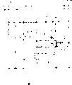
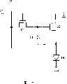
将参照图1说明本发明的像素的基本结构。图1中所示的像素具有晶体管110、第一开关111、第二开关112、第三开关113、第四开关114、第一电容元件115、第二电容元件116和发光元件117。注意,像素连接到信号线118、第一扫描线119、第二扫描线120、第三扫描线121、电源线122、以及电位供应线123。在本实施方式中,晶体管110是N沟道型晶体管,并且当其栅-源电压(Vgs)超过阈值电压(Vth)时处于导通状态。另外,发光元件117的像素电极用作阳极且其相对电极124用作阴极。注意,将晶体管的栅-源电压示为Vgs、将漏-源电压示为Vds、将阈值电压示为Vth、将累积在第一电容元件115及第二电容元件116中的电压分别示为Vc1及Vc2,并且将电源线122、电位供应线123、以及信号线118也分别称为第一布线、第二布线、以及第三布线。此外,也可以将第一扫描线119、第二扫描线120、以及第三扫描线121分别称为第四布线、第五布线、以及第六布线。The basic structure of a pixel of the present invention will be described with reference to FIG. 1 . The pixel shown in FIG. 1 has a
晶体管110的第一电极(源电极及漏电极的一方)连接到发光元件117的像素电极,其第二电极(源电极及漏电极的另一方)通过第二开关112连接到电源线122,并且其栅电极通过第三开关113及第二开关112与电源线122连接。注意,第三开关113连接在晶体管110的栅电极和第二开关112之间。The first electrode (one of the source electrode and the drain electrode) of the
另外,若以晶体管110的栅电极和第三开关113的连接点作为节点130,节点130通过第一电容元件115及第一开关111与信号线118连接。换句话说,第一电容元件115的第一电极通过第一开关111连接到信号线118,并且其第二电极连接到晶体管110的栅电极。另外,第一电容元件115的第一电极也通过第四开关114与电位供应线123连接。节点130也通过第二电容元件116与晶体管110的第一电极连接。换句话说,第二电容元件116的第一电极连接到晶体管110的栅电极,并且其第二电极连接到晶体管110的第一电极。这些电容元件可以通过由布线、半导体层或电极夹绝缘膜来形成,或者根据情况,也可以如图55所示那样使用晶体管110的栅极电容而省略第二电容元件116。将这些保持电压的单元称为保持电容。此外,将节点130与连接有第一电容元件115的第二电极和第二电容元件116的第一电极的布线的连接点作为节点131,将晶体管110的第一电极与连接有第二电容元件116的第二电极和发光元件117的像素电极的布线的连接点作为节点132,以及将晶体管110的第二电极与连接有第二开关112和第三开关113的布线的连接点作为节点133。In addition, if the connection point between the gate electrode of the
另外,通过向第一扫描线119、第二扫描线120和第三扫描线121输入信号来分别控制第一开关111、第二开关112、第三开关113、以及第四开关114的接通和关断。In addition, by inputting signals to the
向信号线118输入相当于视频信号的根据像素灰度的信号,即对应于亮度数据的电位。To the
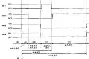
接着,将参照图2的时序图及图3A至3D说明图1所示的像素的工作。注意,在图2中将相当于显示一个画面图像的期间的一个帧期间分成初始化期间、阈值电压写入期间、数据写入期间及发光期间。另外,将初始化期间、阈值电压写入期间和数据写入期间统称为寻址期间。对一个帧期间的长度没有特别限制,但是优选为1/60秒以下,以图像观察者不感觉到闪烁(flicker)。Next, the operation of the pixel shown in FIG. 1 will be described with reference to the timing chart of FIG. 2 and FIGS. 3A to 3D. Note that in FIG. 2 , one frame period corresponding to a period for displaying one screen image is divided into an initialization period, a threshold voltage writing period, a data writing period, and a light emission period. In addition, the initialization period, the threshold voltage writing period, and the data writing period are collectively referred to as an address period. The length of one frame period is not particularly limited, but is preferably 1/60 second or less so that the viewer of the image does not feel flicker.
注意,向发光元件117的相对电极124输入V1的电位(V1:任意数)。另外,若将为了发光元件117发光而至少需要的电位差设定为VEL,向电源线122输入V1+VEL+Vth+α(α:任意的正数)的电位。换句话说,电源线122的电位是V1+VEL+Vth+α以上即可。电位供应线123的电位没有特别的限定,但优选在输入到形成有像素的面板中的电位范围内。这样做,就不需要另行制造电源。注意,在这里,将电位供应线123的电位设定为V2。Note that the potential of V1 (V1: arbitrary number) is input to the
首先,在图2的期间(A)及图3A所示的初始化期间中使第一开关111关断,并且使第二开关112、第三开关113、以及第四开关114接通。此时,晶体管110处于导通状态,在第一电容元件115中保持V1+VEL+Vth+α-V2,在第二电容元件116中保持Vth+α。注意,在初始化期间中,在第一电容元件115中保持预定电压,并且在第二电容元件116中保持至少高于Vth的电压即可。First, in the period (A) of FIG. 2 and the initialization period shown in FIG. 3A , the
在图2的期间(B)及图3B所示的阈值电压写入期间中,使第二开关112关断。因此,晶体管110的第一电极,即源电极的电位逐渐上升,当晶体管110的栅-源电压Vgs达到阈值电压(Vth)时,晶体管110处于非导通状态。因此,保持在第二电容元件116中的电压Vc2大约是Vth。In the period (B) of FIG. 2 and the threshold voltage writing period shown in FIG. 3B , the
在后续的图2的期间(C)及图3C所示的数据写入期间中,在使第三开关113及第四开关114关断之后,使第一开关111接通,并且从信号线118输入对应于亮度数据的电位(V2+Vdata)。此时,当将第一电容元件115、第二电容元件116、以及发光元件117的静电容量分别设定为C1、C2、以及C3时,C3>>C1、C2,从而可以将保持在第二电容元件116中的电压Vc2表示为公式1。In the subsequent period (C) of FIG. 2 and the data writing period shown in FIG. 3C, after the
[公式1][Formula 1]
注意,当决定从信号线118供应的电位时需要C1和C2,但是它们的关系不特别限定。注意,在C1>C2时,因为可以减少由于亮度的变化而引起的Vdata的振幅,所以可以降低耗电量。另一方面,在C2>C1时,可以抑制周围的开关的接通或关断、以及由于截止电流导致的Vc2的变化。因为这些相反的效果,所以优选C1和C2相等,并且第一电容元件115和第二电容元件116的大小相同。Note that C1 and C2 are required when deciding the potential supplied from the
注意,当要在后续的发光期间中使发光元件117不发光时,输入Vdata≤0的电位即可。Note that when the light-emitting
接下来,在图2的期间(D)及图3D所示的发光期间中,在使第一开关111关断之后,使第二开关112接通。此时,晶体管110的栅-源电压为Vgs=Vth+Vdata×(C1/(C1+C2)),对应于亮度数据的电流流到晶体管110及发光元件117,从而发光元件117发光。当然,对于从信号线118输入的对应于亮度数据的电位而言,考虑到晶体管110的栅-源电压为Vgs=Vth+Vdata×(C1/(C1+C2))来决定Vdata。Next, in the period (D) of FIG. 2 and the light emitting period shown in FIG. 3D , after the
注意,在使晶体管110在饱和区工作的情况下,流过发光元件117的电流I由公式2表示。Note that the current I flowing through the
[公式2][Formula 2]
此外,在使晶体管110在线性区工作的情况下,流过发光元件117的电流I由公式3表示。In addition, the current I flowing through the
[公式3][Formula 3]
这里,W是指晶体管110的沟道宽度,L为沟道长度,μ为迁移率,以及Cox为存储电容。Here, W refers to the channel width of the
根据公式2及3,无论晶体管110的工作区是饱和区还是线性区,流过发光元件117的电流都不依赖于晶体管110的阈值电压(Vth)。因此,可以抑制由于晶体管110的阈值电压的不均匀性而导致的电流值的不均匀性,并且可以向发光元件117供应对应于亮度数据的电流。According to formulas 2 and 3, the current flowing through the
据此,可以抑制由于晶体管110的阈值电压的不均匀性而导致的亮度的不均匀性。另外,因为使在将相对电极124的电位固定于恒定值的状态下工作,所以可以降低耗电量。According to this, unevenness in luminance due to unevenness in the threshold voltage of the
而且,在使晶体管110在饱和区中工作的情况下,还可以抑制由发光元件117的退化而导致的亮度的不均匀性。注意,发光元件117的退化不局限于其电流电压特性变化为与退化之前相比平行移动的情况。例如包括如下情况:当特性的倾斜和特性由曲线表现时,其微分值与退化之前的微分值不同。当发光元件117退化时,发光元件117的VEL增加,并且晶体管110的第一电极,即源电极的电位上升。此时,晶体管110的源电极连接到第二电容元件116的第二电极,晶体管110的栅电极连接到第二电容元件116的第一电极,并且栅电极处于浮动状态。因此,随着源极电位的上升,晶体管110的栅极电位也上升相同的电位。因此,由于晶体管110的Vgs没有改变,所以即使发光元件退化也不会影响到流过晶体管110及发光元件117的电流。注意,在公式2中也可以知道流过发光元件117的电流I不依赖于源极电位或漏极电位。Also, in the case of operating the
因此,在使晶体管110在饱和区中工作的情况下,可以抑制由于晶体管110的阈值电压的不均匀性及发光元件117的退化而导致的流过晶体管110的电流的不均匀性。Therefore, in the case of operating the
注意,在使晶体管110在饱和区中工作的情况下,当显著增加漏电压时,沟道长度L越短,因为击穿现象而越容易流过大量电流。Note that in the case of operating the
另外,当漏极电压增加超过夹断电压(pinch-off voltage)时,夹断点(pinch-off point)向源极一侧移动,并且实质上起到沟道作用的有效沟道长度减少。由此,电流值增大。将该现象称作沟道长度调制。注意,夹断点是指沟道消失且在栅极下的沟道厚度为0的边界部,夹断电压是指当夹断点处于漏极端部时的电压。沟道长度L越短,该现象也越容易发生。例如,在图4中示出了根据沟道长度调制的电压-电流特性的示范图。注意,在图4中,晶体管的沟道长度L为(a)>(b)>(c)。In addition, when the drain voltage increases beyond the pinch-off voltage, the pinch-off point moves toward the source side, and the effective channel length substantially functioning as a channel decreases. As a result, the current value increases. This phenomenon is called channel length modulation. Note that the pinch-off point refers to the boundary portion where the channel disappears and the channel thickness under the gate is 0, and the pinch-off voltage refers to the voltage when the pinch-off point is at the end of the drain. The shorter the channel length L, the more likely this phenomenon occurs. For example, an exemplary graph of voltage-current characteristics according to channel length modulation is shown in FIG. 4 . Note that in FIG. 4, the channel length L of the transistor is (a)>(b)>(c).
据此,在使晶体管110在饱和区中工作的情况下,相对于漏-源电压Vds的电流I优选尽可能是恒定的。因此,晶体管110的沟道长度L优选是长的。例如,晶体管的沟道长度L优选大于沟道宽度W。另外,沟道长度L优选为10μm以上且50μm以下,更优选为15μm以上且40μm以下。但是,沟道长度L及沟道宽度W不局限于此。Accordingly, in the case of operating the
因为如上那样可以抑制由于晶体管的阈值电压的不均匀性而导致的电流值的不均匀性,所以在本发明中对于将由所述晶体管控制的电流供应到哪里没有特别限制。因此,有代表性地可以将EL元件(有机EL元件、无机EL元件、或者包含有机物及无机物的EL元件)应用于图1中所示的发光元件117。另外,也可以应用电子发射元件、液晶元件、电子墨水等而代替发光元件117。图5示出了将EL元件517用作发光元件117的实例。注意,图5示出了电流从像素电极511流向相对电极124的情况。Since the non-uniformity of the current value due to the non-uniformity of the threshold voltage of the transistor can be suppressed as above, there is no particular limitation on where the current controlled by the transistor is supplied in the present invention. Therefore, typically, an EL element (an organic EL element, an inorganic EL element, or an EL element including an organic substance and an inorganic substance) can be applied to the
另外,晶体管110只要具有控制供应给发光元件117的电流的功能即可,对于晶体管的种类没有特别限制,而可以使用各种各样的晶体管。例如,将使用晶体半导体膜的薄膜晶体管(TFT)、使用以非晶硅或多晶硅为代表的非单晶半导体膜的薄膜晶体管、使用半导体衬底或SOI衬底形成的晶体管、MOS晶体管、结型晶体管、双极晶体管、使用ZnO或a-InGaZnO等化合物半导体的晶体管、使用有机半导体或碳纳米管的晶体管、或者其它晶体管都可以用作晶体管110。In addition, as long as the
第一开关111选择将对应于亮度数据的电位,即视频信号从信号线118输入到像素的时序,并且主要改变保持在第一电容元件115中的电压及保持在第二电容元件116中的电压,即晶体管110的栅-源电压。另外,第二开关112选择对晶体管110的第二电极供应预定电位的时序。注意,根据情况,对第一电容元件115的第二电极及第二电容元件116的第一电极也供应所述预定电位。第三开关113控制晶体管110的栅电极和第二电极之间的连接,第四开关114选择以每个帧期间将预定电压保持在第一电容元件115中的时序,并且控制对第一电容元件115的第一电极是否供应预定电位。因此,只要第一开关111、第二开关112、第三开关113和第四开关114具有上述功能,就没有特别限制。例如,每个开关都可以是晶体管、二极管、或者组合了它们的逻辑电路。注意,只要可以在上述的时序向像素供应信号或电位,第一开关111、第二开关112、以及第四三开关114就不是必需的。另外,只要实现上述功能,第三开关113也不是必需的。The
例如,当在初始化期间及阈值电压写入期间中可以使第一电容元件115保持预定电压,而且在数据写入期间中可以对像素输入根据像素的灰度的信号时,也可以在像素内不设置第一开关111及第四开关114。而且,若在初始化期间及发光期间中可以对像素供应V1+VEL+Vth+α(α>0),则可以如图43所示那样不必设置第二开关112。图43所示的像素具有晶体管110、第一电容元件115、第三开关113、以及像素电极4300。并且,晶体管110的第一电极(源电极及漏电极的一方)连接到像素电极4300,栅电极通过第三开关113与晶体管110的第二电极连接。另外,晶体管110的栅电极也与第一电容元件115的第二电极连接。注意,在预定期间中,根据灰度的信号,即对应于亮度数据的电位(即,V2+Vdata)及用于使第一电容元件115保持预定电压的任意电位(即,V2)供应到第一电容元件115的第一电极。注意,由于将晶体管110的栅极电容4310利用作保持电容,所以不必设置图1中的第二电容元件116。在这种像素中,也可以通过与图2所示的时序图同样地对各个电极供应所希望的电位,来抑制由于晶体管110的阈值电压的不均匀性而导致的电流值的不均匀性。因此,可以对像素电极4300供应所希望的电流。当然,也可以在图1中也利用晶体管110的栅极电容,而不设置第二电容元件116。For example, when the first
接下来,图6示出了使用N沟道型晶体管作为第一开关111、第二开关112、第三开关113、以及第四开关114的情况。注意,使用相同的附图标记来表示与图1相同的组成部分,并且省略其说明。Next, FIG. 6 shows a case where N-channel type transistors are used as the
第一开关晶体管611相当于图1中的第一开关111,第二开关晶体管612相当于第二开关112,第三开关晶体管613相当于第三开关113,并且第四开关晶体管614相当于第四开关114。注意,晶体管110的沟道长度优选大于第一开关晶体管611、第二开关晶体管612、第三开关晶体管613及第四开关晶体管614中的任一个晶体管的沟道长度。The
第一开关晶体管611的栅电极连接到第一扫描线119,其第一电极连接到信号线118,并且其第二电极连接到第一电容元件115的第一电极。The gate electrode of the
另外,第二开关晶体管612的栅电极连接到第二扫描线120,其第一电极连接到节点133,并且其第二电极连接到电源线122。In addition, the gate electrode of the
第三开关晶体管613的栅电极连接到第三扫描线121,其第一电极连接到节点130,并且其第二电极连接到节点133。The gate electrode of the
另外,第四开关晶体管614的栅电极连接到第三扫描线121,其第一电极连接到第一电容元件115的第一电极,并且其第二电极连接到电位供应线123。In addition, the gate electrode of the
各个开关晶体管当输入到每个扫描线的信号处于H电平时接通,而当被输入的信号处于L电平时关断。The respective switching transistors are turned on when a signal input to each scanning line is at H level, and turned off when the input signal is at L level.
图44图示出了图6所示的像素的布局的一个方式。注意,在下面的实施方式中对于晶体管、电容元件、以及发光元件等的结构进行说明,从而这里仅说明布局方式。另外,作为图44所示的晶体管110及第一开关晶体管611至第四开关晶体管614,使用栅电极位于半导体层下的底栅型晶体管。FIG. 44 illustrates one aspect of the layout of the pixels shown in FIG. 6 . Note that, in the following embodiments, the structures of transistors, capacitive elements, light emitting elements, and the like will be described, so only the layout method will be described here. In addition, as the
图44所示的导电层4410包括用作第一扫描线119的部分和用作第一开关晶体管611的栅电极的部分,导电层4411包括用作信号线118的部分和用作第一开关晶体管611的第一电极的部分。另外,导电层4412包括用作第一开关晶体管611的第二电极的部分、用作第一电容元件115的第一电极的部分、以及用作第四开关晶体管614的第一电极的部分。导电层4413包括用作第一电容元件115的第二电极的部分、用作第二电容元件116的第一电极的部分、以及用作晶体管110的栅电极的部分。另外,该导电层4413通过布线4414与导电层4415连接,导电层4415包括用作第三开关晶体管613的第一电极的部分。导电层4416包括用作第二电容元件116的第二电极的部分和用作晶体管110的第一电极的部分,并且通过接触孔与发光元件的像素电极4455连接。另外,导电层4417包括用作晶体管110的第二电极的部分、用作第三开关晶体管613的第二电极的部分、以及用作第二开关晶体管612的第一电极的部分,导电层4418包括用作电源线122的部分和用作第二开关晶体管612的第二电极的部分。导电层4419包括用作第二扫描线120的部分和用作第二开关晶体管612的栅电极的部分。导电层4420包括用作第三开关晶体管613的栅电极的部分和用作第四开关晶体管614的栅电极的部分,并且通过布线4421与第三扫描线121连接。此外,包括用作第四开关晶体管614的第二电极的部分的导电层4422通过布线4423与电位供应线123连接。The
注意,各导电层的用作第一开关晶体管611的栅电极的部分、用作其第一电极的部分、以及用作其第二电极的部分是分别包括它们的导电层和半导体层4431重叠的部分。用作第二开关晶体管612的栅电极的部分、用作其第一电极的部分、以及用作其第二电极的部分是分别包括它们的导电层和半导体层4432重叠的部分。此外,各导电层的用作第三开关晶体管613的栅电极的部分、用作其第一电极的部分、以及用作其第二电极的部分是分别包括它们的导电层和半导体层4433重叠的部分。用作第四开关晶体管614的栅电极的部分、用作其第一电极的部分、以及用作其第二电极的部分是分别包括它们的导电层和半导体层4434重叠的部分。同样地,在晶体管110中用作栅电极的部分、用作其第一电极的部分、以及用作其第二电极的部分是分别包括它们的导电层和半导体层4430重叠的部分。另外,第一电容元件115形成在导电层4412和导电层4413重叠的部分,并且第二电容元件116形成在导电层4413和导电层4416重叠的部分。Note that the portion serving as the gate electrode of the
另外,导电层4410、导电层4413、导电层4419、导电层4420、第三扫描线121、以及电位供应线123可以使用相同的材料及相同的层来制造。半导体层4430、半导体层4431、半导体层4432、半导体层4433和半导体层4434、以及导电层4411、导电层4412、导电层4415、导电层4416、导电层4417、导电层4418、以及导电层4422可以使用相同的材料及相同的层来制造。另外,可以使用与像素电极4455相同的材料及相同的层来制造布线4414、布线4421、以及布线4423。In addition, the
如图44所示,通过使第一开关晶体管611除外的各个晶体管具有源电极及漏电极的一方电极包围另一方电极的结构,可以使沟道宽度加宽。因此,当将其迁移率低于晶体半导体层的迁移率的非晶半导体层用作构成像素的晶体管的半导体层时,尤其有效。当然,在第一开关晶体管611中也可以采用源电极及漏电极的一方电极包围另一方电极的结构。As shown in FIG. 44 , each transistor except the
接下来,图45的俯视图示出了图6所示的像素的布局的一个方式,该布局方式与图44不同。注意,在图45所示的晶体管110及第一开关晶体管611至第四开关晶体管614中采用栅电极位于半导体层上的正交错型等的顶栅型晶体管。Next, the top view of FIG. 45 shows one aspect of the layout of the pixels shown in FIG. 6 , which is different from that of FIG. 44 . Note that in the
在图45中,导电层4510包括用作第一扫描线119的部分和用作第一开关晶体管611的栅电极的部分,导电层4511包括用作信号线118的部分和用作第一开关晶体管611的第一电极的部分。半导体膜4520包括用作第一开关晶体管611的半导体层的部分、用作第一开关晶体管611的第二电极的部分、用作第四开关晶体管614的第一电极的部分、用作第四开关晶体管614的半导体层的部分、以及用作第一电容元件115的第一电极的部分。注意,半导体膜4520通过布线4512与电位供应线123连接,并且布线4512用作第四开关晶体管614的第二电极。另外,导电层4513包括用作第一电容元件115的第二电极的部分、用作第二电容元件116的第一电极的部分、以及用作晶体管110的栅电极的部分。注意,导电层4513通过用作第三开关晶体管613的第一电极的布线4514与半导体膜4512连接。该半导体膜4521包括用作第三开关晶体管613的半导体层的部分、用作第三开关晶体管613的第二电极的部分、用作第二开关晶体管612的第一电极的部分、用作第二开关晶体管612的半导体层的部分、用作晶体管110的第一电极的部分、用作晶体管110的半导体层的部分、用作晶体管110的第二电极的部分、以及用作第二电容元件116的第二电极的部分。导电层4515包括用作第二扫描线120的部分和用作第二开关晶体管612的栅电极的部分。导电层4516包括用作电源线122的部分和用作第二开关晶体管612的第二电极的部分。导电层4517包括用作第三开关晶体管613的栅电极的部分及用作第四开关晶体管614的栅电极的部分,并且通过布线4518与第三扫描线121连接。注意,发光元件的像素电极4545通过布线4519与半导体膜4521连接。In FIG. 45, the
另外,第一电容元件115形成在半导体膜4520和导电层4513重叠的部分,第二电容元件116形成在半导体膜4521和导电层4513重叠的部分。In addition, the first
另外,导电层4510、导电层4513、导电层4515、导电层4517、第三扫描线121、以及电位供应线123可以使用相同的材料及相同的层来制造。半导体膜4520和半导体膜4521也可以使用相同的材料及相同的层来制造。另外,可以使用与导电层4511相同的材料及相同的层来制造布线4512、布线4514、导电层4516、以及布线4518。In addition, the
注意,像素的布局不局限于上述布局。Note that the layout of pixels is not limited to the above-mentioned layout.
通过与图1相同的工作方法,图6的像素结构中也可以抑制由于晶体管110的阈值电压的不均匀性而导致的电流值的不均匀性。因此,可以向发光元件117供应对应于亮度数据的电流,并且可以抑制亮度的不均匀性。此外,当使晶体管110在饱和区中工作时,也可以抑制由于发光元件117的退化而导致的亮度的不均匀性。By the same working method as in FIG. 1 , the unevenness of the current value caused by the unevenness of the threshold voltage of the
此外,因为可以只使用N沟道型晶体管形成像素,所以可以简化制造工序。另外,将非晶半导体或半非晶半导体等可以用于构成像素的晶体管的半导体层。例如,作为非晶半导体,可以举出非晶硅(a-Si:H)。通过使用这些半导体,可以进一步简化制造工序。因此,可以降低制造成本且提高成品率。In addition, since a pixel can be formed using only N-channel transistors, the manufacturing process can be simplified. In addition, an amorphous semiconductor, a semi-amorphous semiconductor, or the like can be used for the semiconductor layer of the transistor constituting the pixel. For example, amorphous silicon (a-Si:H) is mentioned as an amorphous semiconductor. By using these semiconductors, the manufacturing process can be further simplified. Therefore, manufacturing cost can be reduced and yield can be improved.
注意,由于第一开关晶体管611、第二开关晶体管612、第三开关晶体管613、以及第四开关晶体管614作为简单的开关工作,所以晶体管的极性(导电类型)没有特别限制。但是,最好使用具有低截止电流的晶体管。作为具有低截止电流的晶体管,存在着提供有LDD区的晶体管、具有多栅极结构的晶体管等。另外,所述开关也可以是使用NNote that since the
沟道型晶体管和P沟道型晶体管双方的CMOS型开关。CMOS type switch of both trench type transistor and P-channel type transistor.
此外,只要能够进行与图1相同的工作,开关可以以各种各样的结构来连接,而不局限于图1的结构。图3A至3D说明了在采用图1的像素结构时的工作,从该图3A至3D可以了解的是:在本发明中,初始化期间、阈值电压写入期间、数据写入期间、以及发光期间分别如图53A至53D所示的实线那样导通即可。由此,具有能够满足上述条件地布置开关等并使它们工作的结构即可。In addition, as long as the same operation as that of FIG. 1 can be performed, switches can be connected in various configurations without being limited to the configuration of FIG. 1 . 3A to 3D illustrate the work when the pixel structure of FIG. 1 is adopted. From these FIGS. 3A to 3D, it can be understood that: in the present invention, the initialization period, the threshold voltage writing period, the data writing period, and the light emitting period It is only necessary to conduct as the solid lines shown in FIGS. 53A to 53D . Therefore, what is necessary is just to have the structure which can arrange switches etc. and operate them satisfy|filling the above-mentioned conditions.
另外,在初始化期间中,在第一电容元件115中保持预定电压并且在第二电容元件116中保持至少高于晶体管110的阈值电压Vth的电压即可,从而也可以如图54所示那样节点132通过第五开关5405与电位供应线5401连接。该第五开关5405仅在初始化期间中接通。在图54中,控制第五开关5405的接通或关断的扫描线未图示。注意,电位供应线5401的电位低于V1+VEL的电位即可。更优选是V1以下的电位,通过使它成为这种电位,可以向发光元件117施加反向偏压,所以可以使发光元件中的短路部绝缘并且抑制发光元件的退化。因此,可以延长发光元件的使用寿命。In addition, in the initialization period, it is only necessary to hold a predetermined voltage in the first
接下来,将参照图7说明具有上述的本发明的像素的显示装置。Next, a display device having the pixel of the present invention described above will be described with reference to FIG. 7 .
显示装置具有信号线驱动电路711、扫描线驱动电路712、以及像素部713。像素部713具有:从信号线驱动电路711在列方向上延伸排列的多个信号线S1至Sm、以及电源线P1_1至Pm_1;从扫描线驱动电路712在行方向上延伸排列的多个第一扫描线G1_1至Gn_1、第二扫描线G1_2至Gn_2、第三扫描线G1_3至Gn_3、以及电位供应线P1_2至Pn_2;以及对应于信号线S1至Sm排列成矩阵状的多个像素714。此外,每个像素714与信号线Sj(信号线S1至Sm中的任一个)、电源线Pj_1、第一扫描线Gi_1(扫描线G1_1至Gn_1中的任一个)、第二扫描线Gi_2、第三扫描线Gi_3、以及电位供应线Pi_2连接。The display device has a signal
注意,信号线Sj、电源线Pj_1、第一扫描线Gi_1、第二扫描线Gi_2、第三扫描线Gi_3和电位供应线Pi_2分别相当于图1中的信号线118、电源线122、第一扫描线119、第二扫描线120、第三扫描线121和电位供应线123。Note that the signal line Sj, the power supply line Pj_1, the first scanning line Gi_1, the second scanning line Gi_2, the third scanning line Gi_3, and the potential supply line Pi_2 are respectively equivalent to the
根据从扫描线驱动电路712输出的信号,选择要工作的像素的行,并且同时对属于该行的每个像素进行图2所示的工作。注意,在图2的数据写入期间中,将从信号线驱动电路711输出的视频信号写入到所选择的行的像素中。此时,将对应于每个像素的亮度数据的电位分别输入到各信号线S1至Sm中。According to the signal output from the scanning
如图8所示,例如在第i行的数据写入期间结束后,在属于第i+1行的像素中写入信号。注意,为了表示每行的数据写入期间,图8只示出了可以精确显示该期间的图2的第一开关111的工作。之后,第i行中结束了数据写入期间的像素进入发光期间,并且根据写入到该像素中的信号发光。As shown in FIG. 8 , for example, after the data writing period of the i-th row ends, a signal is written to the pixels belonging to the i+1-th row. Note that in order to represent the data writing period of each row, FIG. 8 only shows the operation of the
因此,若各个行中的数据写入期间不重叠,就可以在各行中自由地设定开始初始化的时间。另外,因为各个像素在其自身的寻址期间除外的期间中可以发光,所以可以使发光期间在一个帧期间中所占的比例(即占空比)非常高,可以大约为100%。因此,可以获得亮度的不均匀性小并且占空比高的显示装置。Therefore, as long as the data writing periods in the respective rows do not overlap, the time to start the initialization can be freely set in the respective rows. In addition, since each pixel can emit light in a period other than its own address period, the ratio (that is, the duty ratio) of the light emission period to one frame period can be very high, and can be approximately 100%. Therefore, a display device with less unevenness in luminance and a high duty ratio can be obtained.
另外,因为也可以将阈值电压写入期间设定为较长,所以可以更准确地将晶体管的阈值电压写入到电容元件中。因此,可以提高显示装置的可靠性。In addition, since the threshold voltage writing period can also be set to be longer, the threshold voltage of the transistor can be more accurately written to the capacitive element. Therefore, the reliability of the display device can be improved.
注意,图7所示的显示装置的结构是一个实例,而本发明不局限于此。例如,电位供应线P1_2至Pn_2不一定要排列成与第一扫描线G1_1至Gn_1平行,也可以排列成与信号线S1至Sm平行。另外,电源线P1_1至Pm_1也不一定要排列成与信号线S1至Sm平行,也可以排列成与第一扫描线G1_1至Gn_1平行。Note that the structure of the display device shown in FIG. 7 is an example, and the present invention is not limited thereto. For example, the potential supply lines P1_2 to Pn_2 do not have to be arranged parallel to the first scan lines G1_1 to Gn_1, and may also be arranged to be parallel to the signal lines S1 to Sm. In addition, the power lines P1_1 to Pm_1 are not necessarily arranged to be parallel to the signal lines S1 to Sm, and may also be arranged to be parallel to the first scan lines G1_1 to Gn_1.
在本实施方式中,虽然示出了使用相同的扫描线即第三扫描线121来控制第三开关113及第四开关114的接通或关断的情况,但也可以分别使用不同的扫描线并且根据图2的时序图来控制各个开关。In this embodiment, although the
注意,阈值电压的不均匀性除了包括在像素之间的每个晶体管的阈值电压的差异以外,还包括当关注于一个晶体管时的阈值电压的经时变化。而且,各个晶体管的阈值电压的差异还包括由于当制造晶体管时的晶体管特性不同而造成的差异。注意,这里所说的晶体管是指具有向发光元件等的负载供应电流的功能的晶体管。Note that the non-uniformity of the threshold voltage includes, in addition to the difference in the threshold voltage of each transistor between pixels, the change over time of the threshold voltage when focusing on one transistor. Furthermore, the difference in the threshold voltage of each transistor also includes a difference due to a difference in transistor characteristics when the transistor is manufactured. Note that the transistor referred to here refers to a transistor having a function of supplying current to a load such as a light emitting element.
实施方式2Embodiment 2
在本实施方式中,将具有与实施方式1不同的结构的像素示出于图9A。注意,使用相同的附图标记来表示与实施方式1相同的组成部分,并且省略相同部分或者具有相似功能的部分的详细说明。In this embodiment, a pixel having a structure different from that of
图9A中所示的像素包括晶体管110、第一开关111、第二开关112、第三开关113、整流元件914、第一电容元件115、第二电容元件116和发光元件117。注意,像素连接到信号线118、第一扫描线119、第二扫描线120、第三扫描线921、第四扫描线922、以及电源线122。图9A所示的像素具有使用整流元件914代替图1中的第四开关114的结构,其中第一电容元件115的第一电极通过整流元件914与第四扫描线922连接。换句话说,连接整流元件914,以使电流从第一电容元件115的第一电极流向第四扫描线922。当然,可以如实施方式1所示那样使用晶体管等作为第一开关111、第二开关112、以及第四开关114。另外,对于整流元件914,不仅可以使用图9B至9D所示的肖特基势垒二极管951、PIN二极管952或PN二极管953等,也可以使用如图9E及9F所示的二极管连接的晶体管954或晶体管955等。但是,至于晶体管954及晶体管955,需要根据流过电流的方向适当地选择晶体管的极性。The pixel shown in FIG. 9A includes a
当向第四扫描线922输入H电平信号时电流不流过整流元件914,而当向第四扫描线922输入L电平信号时电流流过整流元件914。因此,当以与图1中所示的像素相同的方式使图9A至9F中的像素工作时,在初始化期间及阈值电压写入期间中向第四扫描线922输入L电平信号,并且在其它期间中输入H电平信号。不仅向整流元件914流过电流,而且若与实施方式1那样将对应于输入到像素的亮度数据的电位设定为(V2+Vdata),则需要使第二电容元件116的第一电极的电位降低到V2,因此,L电平信号的电位是V2减整流元件914的正方向的阈值电压的电位。但是,V2是任意的值,并且当要在发光期间中使发光元件117不发光时,输入Vdata=0的电位即可。另外,因为如上述那样只要使整流元件914不流过电流即可,所以H电平信号大于从V2减去整流元件914的正方向的阈值电压的值即可。Current does not flow through the rectifying
考虑上述情况,通过以与图1同样的方式进行工作,图9A至9F的像素结构中也可以抑制由于晶体管110的阈值电压的不均匀性而导致的电流值的不均匀性。因此,可以向发光元件117供应对应于亮度数据的电流,并且能够抑制亮度的不均匀性。另外,当使晶体管110在饱和区中工作时,还可以抑制由于发光元件117的退化而导致的亮度的不均匀性。Considering the above, by operating in the same manner as in FIG. 1 , unevenness in current value due to unevenness in the threshold voltage of the
此外,可以将本实施方式所示的像素应用于图7的显示装置。与实施方式1同样,若各个行中的数据写入期间不重叠,就可以在各行中自由地设定开始初始化的时间。另外,因为每个像素除了在其自身的寻址期间外可以发光,所以可以使发光期间在一个帧期间中所占的比例(即占空比)非常高,可以大约为100%。因此,可以获得亮度的不均匀性小并且占空比高的显示装置。In addition, the pixels described in this embodiment mode can be applied to the display device shown in FIG. 7 . As in the first embodiment, as long as the data writing periods in the respective rows do not overlap, the time to start the initialization can be freely set in the respective rows. In addition, since each pixel can emit light except during its own addressing period, the proportion of the light emitting period in one frame period (ie, the duty cycle) can be very high, which can be about 100%. Therefore, a display device with less unevenness in luminance and a high duty ratio can be obtained.
另外,因为可以将阈值电压写入期间设定为较长,所以可以更准确地将控制流向发光元件中的电流值的晶体管的阈值电压写入到电容元件中。因此,提高显示装置的可靠性。In addition, since the threshold voltage writing period can be set longer, the threshold voltage of the transistor controlling the value of the current flowing to the light emitting element can be more accurately written in the capacitive element. Therefore, the reliability of the display device is improved.
本实施方式除了与上述图1以外,还可以与其它实施方式所示的像素结构自由地组合。即,整流元件914还可以应用于其他实施方式所示的像素。In addition to the above-mentioned FIG. 1 , this embodiment can also be freely combined with the pixel structures shown in other embodiments. That is, the rectifying
实施方式3Embodiment 3
在本实施方式中,将具有与实施方式1及2不同结构的像素示出于图10A和10B及图11。具体而言,将说明具有使用其他布线代替图1所示的电位供应线123的结构的像素。注意,只要可以向第一电容元件115的第一电极供应任意电位即可,所以可以具有上述结构。使用相同的附图标记来表示与实施方式1相同的组成部分,并且省略相同部分或者具有相似功能的部分的详细说明。In this embodiment mode, pixels having structures different from those in
图10A所示的像素具有晶体管110、第一开关111、第二开关112、第三开关113、第四开关114、第一电容元件115、第二电容元件116和发光元件117。注意,像素连接到信号线118、第一扫描线119、第二扫描线120、第三扫描线121、以及电源线122。The pixel shown in FIG. 10A has a
在实施方式1所示的图1的像素中,第一电容元件115的第一电极通过第四开关114连接到电位供应线123,而在图10A中可以连接到电源线122。这是因为如下缘故:可以在初始化期间及阈值电压写入期间中将预定电压保持在第一电容元件115中地向第一电容元件115的第一电极供应电位即可,而不局限于第一电容元件115的第一电极连接到电位供应线123的结构。因此,可以使用电源线122而代替电位供应线123。像这样,通过使用电源线122代替向第一电容元件115的第一电极供应电位的布线,而可以减少布线数量,从而可以提高开口率。In the pixel of FIG. 1 shown in
另外,也可以如图10B所示那样使第四开关114与第一电容元件115并联连接。换句话说,第一电容元件115的第一电极也可以通过第四开关114连接到节点131。在这种结构中,也可以在初始化期间及阈值电压写入期间中将预定电压保持在第一电容元件115地向第一电容元件115的第一电极供应电位。In addition, as shown in FIG. 10B , the
另外,如图11的像素所示那样将第一电容元件115的第一电极通过第四开关114连接到发光元件117的相对电极124或向相对电极124供应预定电位的布线。即,也可以使用供应给相对电极124的预定电位而代替图1中的从电位供应线123供应的电位。以上述方式,可以减少布线数量,从而可以提高开口率。In addition, as shown in the pixel of FIG. 11 , the first electrode of the first
另外,也可以通过将使第一电容元件115的第一电极和发光元件117的相对电极124连接的布线不仅与相对电极124连接,而且接触于相对电极124且并联延伸,而利用作相对电极124中的辅助布线。当然,辅助布线不仅在一个像素中,也可以延伸到相邻的像素或像素区整体。借助于这种辅助布线,可以实现相对电极124的低电阻化。因此,当减薄相对电极124时,可以防止电阻值的增加。尤其,在使用具有透光性的电极作为相对电极124的情况下很有效。另外,在相对电极的电阻值提高时,可以抑制由于因电压下降产生的相对电极124的不均匀的面电位分布而产生的发光元件117的亮度的不均匀性。因此,可以进一步提高可靠性。In addition, the wiring connecting the first electrode of the first
另外,通过以与实施方式1中相同的方式工作,图10A和10B及图11中所示的像素结构中也能抑制由于晶体管110的阈值电压的不均匀性而导致的电流值的不均匀性。因此,可以向发光元件117供应对应于亮度数据的电流,并且可以抑制亮度的不均匀性。另外,因为在将相对电极的电位固定于恒定值的状态下进行工作,所以可以降低耗电量。注意,尽管晶体管110的工作区没有特别限制,但是,当使晶体管110在饱和区中工作时,也可以抑制由于发光元件117的退化而导致的流过晶体管110的电流的不均匀性。In addition, by operating in the same manner as in
注意,图1中的电位供应线123只要在初始化期间及阈值电压写入期间中向第一电容元件115的第一电极供应任意电位,以在第一电容元件115中保持预定电压即可。因此,代替电位供应线使用的布线不局限于上述布线,只要是在初始化期间及阈值电压写入期间中不改变电位的布线即可。例如,如图12所示那样使用第一扫描线119和第三扫描线121也可以。但是,在使用第三扫描线121的情况下,需要注意第四开关114有时用作实施方式2所示的整流元件来选择开关的种类。Note that the
此外,可以将本实施方式所示的像素应用于图7的显示装置。与实施方式1同样,若各个行中的数据写入期间不重叠,就可以在各行中自由地设定开始初始化的时间。另外,因为每个像素除了在其自身的寻址期间外可以发光,所以可以使发光期间在一个帧期间中所占的比例(即占空比)非常高,可以大约为100%。因此,可以提供亮度的不均匀性小并且占空比高的显示装置。In addition, the pixels described in this embodiment mode can be applied to the display device shown in FIG. 7 . As in the first embodiment, as long as the data writing periods in the respective rows do not overlap, the time to start the initialization can be freely set in the respective rows. In addition, since each pixel can emit light except during its own addressing period, the proportion of the light emitting period in one frame period (ie, the duty cycle) can be very high, which can be about 100%. Therefore, it is possible to provide a display device having a small unevenness in luminance and a high duty ratio.
另外,因为可以将阈值电压写入期间设定为较长,所以可以更准确地将控制流向发光元件中的电流值的晶体管的阈值电压写入到电容元件中。因此,提高显示装置的可靠性。In addition, since the threshold voltage writing period can be set longer, the threshold voltage of the transistor controlling the value of the current flowing to the light emitting element can be more accurately written in the capacitive element. Therefore, the reliability of the display device is improved.
本实施方式可以与其他实施方式所示的像素结构自由地组合,而不局限于上述结构。This implementation manner can be freely combined with the pixel structures shown in other implementation manners, and is not limited to the above structures.
实施方式4Embodiment 4
在本实施方式中,将具有与实施方式1至3不同结构的像素示出于图13至图16。注意,在实施方式1至3中虽然着眼于一个像素来说明,然而,也可以通过在不同像素之间共同使用连接到各个像素的布线,而减少布线的数量。在此情况下,只要正常工作,就可以在不同像素之间共同使用各种布线。例如,可以与相邻的像素共同使用布线,本实施方式中将说明该情况的一例。注意,使用相同的附图标记来表示与实施方式1相同的组成部分,并且省略相同部分或者具有相似功能的部分的详细说明。In this embodiment, pixels having structures different from those in
图13中所示的像素1300包括晶体管110、第一开关111、第二开关112、第三开关113、第四开关114、第一电容元件115、第二电容元件116和发光元件117。注意,像素1300连接到信号线118、第一扫描线119、第二扫描线120、第三扫描线121、以及前一列的电源线1322。A
在实施方式1所示的图1的像素中,第一电容元件115的第一电极通过第四开关114连接到电位供应线123,而在图13中可以连接到前一列的电源线1322。这是因为如下缘故:可以在初始化期间及阈值电压写入期间中将预定电压保持在第一电容元件115中地向第一电容元件115的第一电极供应电位即可,而不局限于第一电容元件115的第一电极连接到电位供应线123的结构。因此,可以采用前一列的电源线1322而代替电位供应线123。像这样,像素1300与前一列的像素共同使用布线,而可以减少布线数量,从而可以提高开口率。In the pixel shown in FIG. 1 shown in
注意,通过以与实施方式1中相同的方式进行工作,图13中所示的像素结构中也能抑制由于晶体管110的阈值电压的不均匀性而导致的电流值的不均匀性。因此,可以向发光元件117中供应对应于亮度数据的电流,并且可以抑制亮度的不均匀性。另外,因为在将相对电极的电位固定于恒定值的状态下进行工作,所以可以降低耗电量。注意,尽管晶体管110的工作区没有特别限制,但是当在饱和区中工作时,可以抑制由于发光元件117的退化而导致的流过晶体管110的电流的不均匀性。Note that, by operating in the same manner as in
另外,如图14的像素1400所示,也可以与下一行的第一扫描线1419共同使用图1中的电位供应线123。在像素1400中也可以进行与实施方式1相同的工作。但是,需要像素1400所属的行的初始化期间及阈值电压写入期间与共同使用布线的行的数据写入期间不重叠来工作。In addition, as shown in the
另外,如图15的像素1500所示,也可以与下一行的第二扫描线1520共同使用图1中的电位供应线123。在像素1500中也可以进行与实施方式1相同的工作。但是,需要像素1500所属的行的初始化期间及阈值电压写入期间与共同使用布线的行的阈值电压写入期间及数据写入期间重叠或完全不重叠来工作。换句话说,对供应给第一电容元件115的第一电极的电位使用于使第二开关112接通的信号或关断的信号中的任一个。In addition, as shown in the
另外,除了上述以外,也可以如图16所示那样与前一行的第三扫描线1621共同使用图1中的电位供应线123。但是,需要像素1600所属的行的初始化期间及阈值电压写入期间与共同使用布线的行的阈值电压写入期间及数据写入期间不重叠来工作。In addition to the above, as shown in FIG. 16 , the
注意,尽管在本实施方式中说明了与上一列的电源线、下一行或上一行的扫描线共同使用图1的电位供应线123的情况,但是只要能在初始化期间及阈值电压写入期间中向第一电极供应电位,以在第一电容元件115中保持预定电压,就可以使用其它布线。Note that although the case of using the
而且,可以将本实施方式所示的像素应用于图7的显示装置。注意,在图13至图16中所记载的每个像素的工作限制及各行中数据写入期间不重叠的范围内,可以在各行中自由地设定开始初始化的时间。另外,因为各个像素在其自身的寻址期间以外的期间中可以发光,所以可以使发光期间在一个帧期间中所占的比例(即占空比)非常高,可以大约为100%。因此,可以提供亮度的不均匀性小并且占空比高的显示装置。Furthermore, the pixels described in this embodiment mode can be applied to the display device shown in FIG. 7 . Note that the time to start initialization can be freely set in each row within the limits of the operation of each pixel described in FIGS. 13 to 16 and the data writing periods in each row do not overlap. In addition, since each pixel can emit light in a period other than its own address period, the ratio (that is, the duty ratio) of the light emission period to one frame period can be very high, and can be approximately 100%. Therefore, it is possible to provide a display device having a small unevenness in luminance and a high duty ratio.
另外,因为可以将阈值电压写入期间设定为较长,所以可以更准确地将控制流向发光元件中的电流值的晶体管的阈值电压写入到电容元件中。因此,提高显示装置的可靠性。In addition, since the threshold voltage writing period can be set longer, the threshold voltage of the transistor controlling the value of the current flowing to the light emitting element can be more accurately written in the capacitive element. Therefore, the reliability of the display device is improved.
本实施方式可以与其他实施方式所示的像素结构自由地组合来实施,而不局限于上述结构。This embodiment mode can be freely combined with the pixel structures shown in other embodiments, and is not limited to the above structures.
实施方式5
在本实施方式中,将具有与实施方式1不同结构的像素示出于图29。注意,使用相同的附图标记来表示与实施方式1相同的组成部分,并且省略了相同部分或者具有相似功能的部分的详细说明。In this embodiment, a pixel having a structure different from that of
图29所示的像素包括晶体管2910、第一开关111、第二开关112、第三开关113、第四开关114、第一电容元件115、第二电容元件116和发光元件117。注意,像素连接到信号线118、第一扫描线119、第二扫描线120、第三扫描线121、电源线122、以及电位供应线123。The pixel shown in FIG. 29 includes a
本实施方式中的晶体管2910是串联连接了两个晶体管的多栅极晶体管,并且设在与实施方式1中的晶体管110相同的位置上。但是,串联连接的晶体管的数量没有特别限制。The
通过以与图1中的像素相同的方式使图29所示的像素工作,可以抑制由于晶体管2910的阈值电压的不均匀性而导致的电流值的不均匀性。因此,可以向发光元件117中供应对应于亮度数据的电流,并且可以抑制亮度的不均匀性。另外,因为在将相对电极的电位固定于恒定值的状态下进行工作,所以可以降低耗电量。注意,尽管晶体管2910的工作区没有特别限制,但是在饱和区工作时,也可以抑制由于发光元件117的退化而导致的流过晶体管2910的电流的不均匀性。By operating the pixel shown in FIG. 29 in the same manner as the pixel in FIG. 1 , unevenness in current value due to unevenness in the threshold voltage of the
当串联连接的两个晶体管的沟道宽度彼此相等时,本实施方式中的晶体管2910的沟道长度L等于各个晶体管的沟道长度的总和。因此,不管漏-源电压Vds如何,在饱和区中都容易获得更加接近恒定值的电流值。特别是当难以制造具有长沟道长度L的晶体管时,晶体管2910是有效的。注意,两个晶体管的连接部用作电阻。When the channel widths of two transistors connected in series are equal to each other, the channel length L of the
注意,只要晶体管2910具有控制供应给发光元件117的电流值的功能即可,晶体管的种类没有特别限制。因此,使用晶体半导体膜的薄膜晶体管(TFT)、使用以非晶硅或多晶硅为代表的非单晶半导体膜的薄膜晶体管、使用半导体衬底或SOI衬底形成的晶体管、MOS晶体管、结型晶体管、双极晶体管、使用ZnO或a-InGaZnO等化合物半导体的晶体管、使用有机半导体或碳纳米管的晶体管、或者其它晶体管都可以应用。Note that the type of transistor is not particularly limited as long as the
此外,与图1中所示的像素相同,在图29所示的像素中,可以将晶体管等用于第一开关111、第二开关112、第三开关113和第四开关114。Also, in the pixel shown in FIG. 29 , transistors and the like can be used for the
此外,可以将本实施方式所示的像素应用于图7的显示装置。与实施方式1相同,若各个行中的数据写入期间不重叠,就可以在各个行中自由地设定开始初始化的时间。另外,因为各个像素在其自身的寻址期间以外的期间中可以发光,所以可以使发光期间在一个帧期间中所占的比例(即占空比)非常高,可以大约为100%。因此,可以提供亮度的不均匀性小并且占空比高的显示装置。In addition, the pixels described in this embodiment mode can be applied to the display device shown in FIG. 7 . As in the first embodiment, as long as the data writing periods in the respective rows do not overlap, the time to start the initialization can be freely set in the respective rows. In addition, since each pixel can emit light in a period other than its own address period, the ratio (that is, the duty ratio) of the light emission period to one frame period can be very high, and can be approximately 100%. Therefore, it is possible to provide a display device having a small unevenness in luminance and a high duty ratio.
另外,也因为可以将阈值电压写入期间设定为较长,所以可以更准确地将控制流向发光元件中的电流值的晶体管的阈值电压写入到电容元件中。因此,提高显示装置的可靠性。Also, since the threshold voltage writing period can be set longer, the threshold voltage of the transistor that controls the value of the current flowing to the light emitting element can be written more accurately in the capacitive element. Therefore, the reliability of the display device is improved.
注意,晶体管2910不局限于将晶体管串联连接的结构,也可以具有像图30所示的晶体管3010那样将晶体管并联连接的结构。晶体管3010可以向发光元件117供应更大的电流。另外,因为晶体管的特性被两个并联连接的晶体管平均,所以可以降低构成晶体管3010的晶体管本来的特性的不均匀性。由此,若不均匀性小,可以更容易地抑制由于晶体管的阈值电压的不均匀性而导致的电流值的不均匀性。Note that the
此外,如图29的晶体管2910那样,还可以将晶体管3010中的并联连接的各个晶体管串联连接。In addition, like the
本实施方式不局限于上述所示的结构,而可以与其他实施方式所示的像素结构自由地组合来实施。就是说,晶体管2910或晶体管3010可以应用于其他实施方式所示的像素结构中。This embodiment is not limited to the structures shown above, and can be freely combined with the pixel structures shown in other embodiments. That is to say, the
实施方式6
在本实施方式中,将参照图31说明一种像素结构,其中通过在每个期间中分别使用控制供应给本发明的像素中的发光元件的电流值的晶体管,而使晶体管的经时退化平均化。In this embodiment mode, a pixel structure will be described with reference to FIG. 31 in which the time-dependent deterioration of the transistors is averaged by using transistors for controlling the current value supplied to the light-emitting element in the pixel of the present invention for each period respectively. change.
图31所示的像素包括第一晶体管3101、第二晶体管3102、第一开关3111、第二开关3112、第三开关3113、第四开关3114、第五开关3103、第六开关3104、第一电容元件3115、第二电容元件3116和发光元件3117。注意,像素连接到信号线3118、第一扫描线3119、第二扫描线3120、第三扫描线3121、电源线3122、以及电位供应线3123。而且,尽管图31中未图示,但是像素还连接到控制第五开关3103及第六开关3104的接通和关断的第四扫描线及第五扫描线。在本实施方式中,第一晶体管3101及第二晶体管3102都是N沟道型晶体管,并且每个晶体管当其栅-源电压(Vgs)超过阈值电压时分别处于导通状态。另外,发光元件3117的像素电极是阳极而其相对电极3124是阴极。注意,将晶体管的栅-源电压示为Vgs,并且将存储在第一电容元件3115及第二电容元件3116中的电压分别示为Vc1、Vc2。此外,将第一晶体管3101的阈值电压示为Vth1,并且将第二晶体管3102的阈值电压示为Vth2。电源线3122、电位供应线3123、以及信号线3118也分别称为第一布线、第二布线、以及第三布线。The pixel shown in FIG. 31 includes a
第一晶体管3101的第一电极(源电极及漏电极的一方)通过第五开关3103连接到发光元件3117的像素电极,其第二电极(源电极及漏电极的另一方)通过第二开关3112连接到电源线3122。另外,第一晶体管3101的栅电极也通过第三开关3113及第二开关3112与电源线3122连接。注意,第三开关3113连接在第一晶体管3101的栅电极和第二开关3112之间,并且以第一晶体管3101的第二电极与连接第二开关3112和第三开关3113的布线的连接点为节点3133。The first electrode (one of the source electrode and the drain electrode) of the
第二晶体管3102的第一电极(源电极及漏电极的一方)通过第六开关3104连接到发光元件3117的像素电极,其第二电极(源电极及漏电极的另一方)连接到第一晶体管3101的第二电极。另外,当以第一晶体管3101的第二电极和第二晶体管3102的第二电极的连接点为节点3132时,节点3132与节点3133连接。此外,第二晶体管3102的栅电极通过第三开关3113连接到节点3133。另外,第一晶体管3101的栅电极和第二晶体管3102的栅电极彼此连接。The first electrode (one of the source electrode and the drain electrode) of the
另外,当以第一晶体管3101及第二晶体管3102的栅电极与第三开关3113的连接点为节点3130时,节点3130通过第一电容元件3115及第一开关3111与信号线3118连接。即,第一电容元件3115的第一电极通过第一开关3111连接到信号线3118,而其第二电极连接到第一晶体管3101及第二晶体管3102的栅电极。另外,第一电容元件3115的第一电极通过第四开关3114也与电位供应线3123连接。节点3130还通过第二电容元件3116也与发光元件3117的像素电极连接。换句话说,第二电容元件3116的第一电极连接到第一晶体管3101及第二晶体管3102的栅电极,并且其第二电极通过第五开关3103及第六开关3104连接到第一晶体管3101及第二晶体管3102的第一电极。这些电容元件可以通过由布线、半导体层或电极夹绝缘膜来形成,或者根据情况,使用第一晶体管3101及第二晶体管3102的栅极电容,而不形成第二电容元件3116。In addition, when the connection point between the gate electrodes of the
注意,通过向第一扫描线3119、第二扫描线3120和第三扫描线3121输入信号来分别控制第一开关3111、第二开关3112、第三开关3113、以及第四开关3114的接通和关断。如上所述,在图31中,省略了控制第五开关3103及第六开关3104的接通和关断的扫描线。Note that the on and off of the
向信号线3118输入相当于视频信号的根据像素灰度的信号,即对应于亮度数据的电位。To the
接着,将参照图32的时序图说明图31所示的像素的工作。注意,在图32中将相当于显示一个画面图像的期间的一个帧期间分成初始化期间、阈值电压写入期间、数据写入期间、以及发光期间。Next, the operation of the pixel shown in FIG. 31 will be described with reference to the timing chart of FIG. 32 . Note that in FIG. 32 , one frame period corresponding to a period in which one screen image is displayed is divided into an initialization period, a threshold voltage writing period, a data writing period, and a light emission period.
注意,向发光元件3117的相对电极3124输入V1的电位(V1:任意数)。另外,若将为使发光元件3117发光至少需要的电位差设定为VEL,向电源线3122输入V1+VEL+Vth+α(α:任意的正数)的电位。换句话说,电源线3122具有V1+VEL+Vth+α以上的电位即可。注意,Vth是Vth1和Vth2中的大一方的值。电位供应线3123的电位没有特别的限定,但优选在输入到形成有像素的面板中的电位范围内。这样做,就不需要另行制造电源。注意,在这里,将电位供应线3123的电位设定为V2。Note that the potential of V1 (V1: arbitrary number) is input to the
首先,在图32的期间(A)所示的初始化期间中,使第一开关3111及第六开关3104关断,并且使第二开关3112、第三开关3113、第四开关3114、以及第五开关3103接通。此时,第一晶体管3101处于导通状态,并且在第一电容元件3115中保持V1+VEL+Vth+α-V2,在第二电容元件3116中保持Vth+α。另外,在该初始化期间中,在第一电容元件3115保持预定电压且在第二电容元件3116保持至少高于Vth1的电压即可。First, in the initialization period shown in period (A) of FIG. The
在图32的期间(B)所示的阈值电压写入期间中,使第二开关3112关断。因此,第一晶体管3101的第一电极,即源电极的电位逐渐上升,当第一晶体管3101的栅-源电压Vgs成为阈值电压(Vth1)时,第一晶体管3101处于非导通状态。因此,保持在第二电容元件3116中的电压Vc2大致成为Vth1。In the threshold voltage writing period shown in the period (B) of FIG. 32 , the
在图32的期间(C)所示的后续的数据写入期间中,在使第三开关3113及第四开关3114关断之后,使第一开关3111接通,并且从信号线3118输入对应于亮度数据的电位(V2+Vdata)。此时,当将第一电容元件3115、第二电容元件3116、以及发光元件3117的静电容量分别设定为C1、C2、以及C3时,C3>>C1、C2,从而可以将保持在第二电容元件3116中的电压Vc2成为Vth1+Vdata×(C1/(C1+C2))。In the subsequent data writing period shown in period (C) of FIG. 32 , after the
注意,当决定从信号线3118供应的电位时需要C1和C2,但是它们的关系不特别限定。注意,在C1>C2时,因为可以减少由于亮度的变化而引起的Vdata的振幅,所以可以降低耗电量。另一方面,在C2>C1时,可以抑制周围的开关的接通或关断、以及由于截止电流导致的Vc2的变化。因为这些相反的效果,所以优选C1和C2相等,并且第一电容元件3115和第二电容元件3116的大小相同。Note that C1 and C2 are required when deciding the potential supplied from the
注意,当要在后续的发光期间中使发光元件3117不发光时,输入Vdata≤0的电位即可。Note that when the light-emitting
接着,在图32的期间(D)所示的发光期间中,在使第一开关3111关断之后,使第二开关3112接通。此时,第一晶体管3101的栅-源电压Vgs成为Vth1+Vdata×(C1/(C1+C2)),并且对应于亮度数据的电流流过第一晶体管3101及发光元件3117,从而发光元件3117发光。Next, in the light emitting period shown in the period (D) of FIG. 32 , after the
通过这种工作,无论第一晶体管3101的工作区是饱和区还是线性区,流过发光元件3117的电流都不依赖于第一晶体管3101的阈值电压(Vth1)。Through this operation, the current flowing through the
而且,在图32的期间(E)所示的下一帧期间中的初始化期间中,使第五开关3103关断,并且使第三开关3113、第四开关3114、以及第六开关3104接通。第二晶体管3102处于导通状态,在第一电容元件3115中保持V1+VEL+Vth+α-V2,在第二电容元件3116中保持Vth+α。注意,在该初始化期间中,在第一电容元件3115保持预定电压且在第二电容元件3116中保持至少高于Vth2的电压即可。Furthermore, in the initialization period in the next frame period shown in period (E) of FIG. . The
接着,在图32的期间(F)所示的阈值电压写入期间中,使第二开关3112关断。因此,第二晶体管3102的第一电极,即源电极的电位逐渐上升,当第二晶体管3102的栅-源电压Vgs成为阈值电压(Vth2)时,第二晶体管3102处于非导通状态。因此,保持在第二电容元件3116中的电压Vc2大致成为Vth2。Next, in the threshold voltage writing period shown in the period (F) of FIG. 32 , the
在图32的期间(G)所示的后续的数据写入期间中,在使第三开关3113及第四开关3114关断之后,使第一开关3111接通,并且从信号线3118输入对应于亮度数据的电位(V2+Vdata)。此时,保持在第二电容元件3116中的电压Vc2成为Vth2+Vdata×(C1/(C1+C2))。In the subsequent data writing period shown in period (G) of FIG. 32 , after the
接着,在图32的期间(H)所示的发光期间中,在使第一开关3111关断之后,使第二开关3112接通。此时,第二晶体管3102的栅-源电压Vgs成为Vth2+Vdata×(C1/(C1+C2)),并且对应于亮度数据的电流流过第二晶体管3102及发光元件3117,从而发光元件3117发光。Next, in the light emitting period shown in the period (H) of FIG. 32 , after the
无论第二晶体管3102的工作区是饱和区还是线性区,流过发光元件3117的电流都不依赖于阈值电压(Vth2)。Regardless of whether the operation region of the
因此,通过使用第一晶体管3101或第二晶体管3102控制供应给发光元件的电流,可以抑制由于晶体管的阈值电压的不均匀性而导致的电流值的不均匀性,并且可以向发光元件3117供应对应于亮度数据的电流。注意,通过将第一晶体管3101和第二晶体管3102切换来减轻施加到一个晶体管的负载,而可以减小晶体管的阈值电压的经时变化。Therefore, by controlling the current supplied to the light emitting element using the
据此,可以抑制由于第一晶体管3101和第二晶体管3102的阈值电压而导致的亮度的不均匀性。另外,因为相对电极的电位是恒定的,所以可以降低耗电量。According to this, unevenness in luminance due to threshold voltages of the
而且,当使第一晶体管3101和第二晶体管3102在饱和区中工作的情况下,也可以抑制流过每个晶体管的电流因发光元件3117的退化而产生不均匀性。Also, when the
注意,当使第一晶体管3101和第二晶体管3102在饱和区中工作的情况下,这些晶体管的沟道长度L优选是长的。Note that, in the case of operating the
注意,因为可以抑制由于晶体管的阈值电压的不均匀性而导致的电流值的不均匀性,所以将由所述晶体管控制的电流供应到哪里没有特别限制。因此,可以使用EL元件(有机EL元件、无机EL元件、或者包含有机物及无机物的EL元件)作为图31所示的发光元件3117。另外,也可以使用电子发射元件、液晶元件、电子墨水等而代替发光元件3117。Note that there is no particular limitation to where the current controlled by the transistor is supplied because the non-uniformity of the current value due to the non-uniformity of the threshold voltage of the transistor can be suppressed. Therefore, an EL element (an organic EL element, an inorganic EL element, or an EL element including organic and inorganic substances) can be used as the
另外,只要第一晶体管3101和第二晶体管3102具有控制供应给发光元件3117的电流值的功能即可,晶体管的种类没有特别限制。因此,使用晶体半导体膜的薄膜晶体管(TFT)、使用以非晶硅或多晶硅为代表的非单晶半导体膜的薄膜晶体管、使用半导体衬底或SOI衬底来形成的晶体管、MOS晶体管、耦合晶体管、双极晶体管、使用ZnO或a-InGaZnO等化合物半导体的晶体管、使用有机半导体或碳纳米管的晶体管、或者其它晶体管都可以使用。In addition, as long as the
第一开关3111选择将对应于亮度数据的电位,即信号从信号线3118输入到像素的时序,并且主要改变保持在第一电容元件3115中的电压及保持在第二电容元件3116中的电压,即第一晶体管3101或第二晶体管3102的的栅-源电压。另外,第二开关3112选择对第一晶体管3101或第二晶体管3102的第二电极供应预定电位的时序。注意,根据情况,对第一电容元件3115的第二电极及第二电容元件3116的第一电极也供应所述预定电位。第三开关3113控制第一晶体管3101或第二晶体管3102的栅电极和各个晶体管的第二电极之间的连接,第四开关3114选择以每个帧期间将预定电压保持在第一电容元件3115中的时序,并且控制对第一电容元件3115的第一电极是否供应预定电位。因此,只要第一开关3111、第二开关3112、第三开关3113和第四开关3114具有上述功能,就没有特别限制。例如,每个开关都可以是晶体管、二极管、或者组合了它们的逻辑电路。注意,只要可以在上述的时序向像素供应信号或电位,第一开关3111、第二开关3112、以及第四三开关3114就不是必需的。另外,只要实现上述功能,第三开关3113也不是必需的。The
例如,在使用N沟道型晶体管作为第一开关3111、第二开关3112、第三开关3113、第四开关3114、第五开关3103和第六开关3104的情况下,因为可以只使用N沟道型晶体管形成像素,所以可以简化制造工序。另外,可以将非晶半导体或半非晶半导体等用于构成像素的晶体管的半导体层。例如,作为非晶半导体,可以举出非晶硅(a-Si:H)。通过使用这些半导体,可以进一步简化制造工序。因此,可以降低制造成本且提高成品率。For example, in the case of using N-channel type transistors as the
注意,在使用晶体管作为第一开关3111、第二开关3112、第三开关3113、第四开关3114、第五开关3103和第六开关3104的情况下,晶体管的极性(导电类型)没有特别限制。但是,最好使用具有低截止电流的晶体管。Note that in the case of using transistors as the
另外,如图37中所示,第一晶体管3101及第五开关3103与第二晶体管3102及第六开关3104可以相互交换位置。换句话说,第一晶体管3101及第二晶体管3102的第一电极通过第二电容元件3116连接到第一晶体管3101及第二晶体管3102的栅电极。此外,第一晶体管3101的第二电极通过第五开关3103与节点3132连接,并且第二晶体管3102的第二电极通过第六开关3104与节点3132连接。In addition, as shown in FIG. 37 , the
此外,图31及图37示出了并联设置的元件数量是两个的情况,其中使用晶体管和开关作为一组,即使用第一晶体管3101和第五开关3103作为一组、以及第二晶体管3102和第六开关3104作为一组。但是,并联设置的元件数量没有特别限制。In addition, FIG. 31 and FIG. 37 show the case where the number of elements arranged in parallel is two, wherein a transistor and a switch are used as a set, that is, the
此外,通过将本实施方式所示的像素应用到图7的显示装置,若各行中的数据写入期间不重叠,就可以与实施方式1同样地在各行中自由地设定开始初始化的时间。另外,因为各个像素在其自身的寻址期间以外的期间中可以发光,所以发光期间在一个帧期间中所占的比例(即占空比)可以非常高,可以大约为100%。因此,可以提供亮度的不均匀性小并且占空比高的显示装置。Also, by applying the pixels shown in this embodiment to the display device of FIG. 7 , as in
另外,因为可以将阈值电压写入期间设定为较长,所以可以更准确地将控制流向发光元件中的电流值的晶体管的阈值电压写入到电容元件中。因此,提高显示装置的可靠性。In addition, since the threshold voltage writing period can be set longer, the threshold voltage of the transistor controlling the value of the current flowing to the light emitting element can be more accurately written in the capacitive element. Therefore, the reliability of the display device is improved.
注意,在本实施方式中,也可以如实施方式3所示那样使用相同像素内的布线代替电位供应线3123,也可以与实施方式4同样共同使用电位供应线3123和其它行的布线共用。另外,也可以使用晶体管串联连接的多栅极晶体管或并联设置的晶体管作为第一晶体管3101及第二晶体管3102中的每一个。本实施方式不局限于此,而可以应用于实施方式1至5所示的像素结构。Note that in the present embodiment, the wiring in the same pixel may be used instead of the
实施方式7Embodiment 7
在本实施方式中,说明具有与实施方式1不同结构的像素。使用共同的附图标记来表示与实施方式1相似的元件,并且省略了相同部分或者具有相似功能的部分的详细说明。注意,以与实施方式1相同的方式操作这些部分。In this embodiment, a pixel having a structure different from that of
在本实施方式中,说明强迫阻止电流流向发光元件117的像素结构。换句话说,本实施方式的目的在于获得通过强迫使发光元件处于不发光状态,几乎看不见余像并且使动画特性优越的显示装置。In this embodiment mode, a pixel structure in which current flow to the
图38中显示了这种像素结构之一。图38中所示的像素除了包括晶体管110、第一开关111、第二开关112、第三开关113、第四开关114、第一电容元件115、第二电容元件116和发光元件117以外还包括第五开关3801。另外,像素除了连接到信号线118、第一扫描线119、第二扫描线120、第三扫描线121、电源线122、以及电位供应线123以外,还连接到第四扫描线3802。One such pixel structure is shown in FIG. 38 . The pixel shown in FIG. 38 includes a
在图38中,第五开关3801与第二电容元件116并联连接。因此,当第五开关3801接通时,晶体管110的栅电极和第一电极短路。由此,因为可以使第二电容元件116保持的晶体管110的栅-源电压成为0V,所以晶体管110关断,从而使发光元件117处于不发光状态。注意,通过使用输入到第四扫描线3802的信号逐行扫描像素,来控制第四开关3801的接通和关断。In FIG. 38 , the
根据这种工作,擦除写入在像素中的信号。因此,可以提供迫使发光元件处于不发光状态一直到下一个初始化期间的擦除期间。换句话说,插入黑色显示。因此,不容易看见余像并且可以提高动画特性。According to this operation, a signal written in a pixel is erased. Therefore, an erasing period in which the light emitting element is forced to be in a non-light emitting state until the next initialization period can be provided. In other words, insert a black display. Therefore, afterimages are not easily seen and animation characteristics can be improved.
作为表达显示装置的灰度级的驱动方式,有模拟灰度级方式和数字灰度级方式。模拟灰度级方式包括以模拟方式控制发光元件的发光强度的方式和以模拟方式控制发光元件的发光时间的方式。在两者间,通常使用以模拟方式控制发光元件的发光强度的方式作为模拟灰度级方式。另一方面,在数字灰度级方式中,通过以数字方式控制来使发光元件接通或关断以表达灰度级。数字灰度级方式因为使用数字信号进行处理而具有高的抗噪性。但是,仅有两种状态,即发光状态和不发光状态,从而只能表达两个灰度级。因此,组合使用其它方法实现多级灰度级显示。作为多级灰度级显示的方法,有权重像素的发光面积并选择来进行灰度级显示的面积灰度级方式和权重发光时间并选择来进行灰度级显示的时间灰度级方式。There are an analog grayscale method and a digital grayscale method as driving methods for expressing grayscale levels of a display device. The analog gray scale method includes a method of controlling the light emission intensity of the light emitting element in an analog manner and a method of controlling the light emission time of the light emitting element in an analog manner. Between the two, a method of controlling the light emission intensity of a light-emitting element in an analog manner is generally used as an analog gray scale method. On the other hand, in the digital grayscale method, a light emitting element is turned on or off by digitally controlling to express a grayscale. The digital grayscale method has high noise immunity because it uses digital signals for processing. However, there are only two states, a light-emitting state and a non-light-emitting state, so that only two gray scales can be expressed. Therefore, other methods are used in combination to realize multi-level gray scale display. As a method of multi-level grayscale display, there are area grayscale method in which grayscale display is performed by selecting and weighting the light emitting area of pixels, and time grayscale method in which grayscale display is performed by weighting light emitting time.
在组合数字灰度级方式和时间灰度级方式的情况中,如图39中所示,将一个帧期间分成多个子帧期间(SFn)。各个子帧期间包括寻址期间(Ta)和发光期间(Ts),所述寻址期间(Ta)包括初始化期间、阈值电压写入期间和数据写入期间。注意,在一个帧期间中提供其数量与显示位数n对应的子帧期间。另外,设置各个子帧期间中将发光期间的长度的比例设定为2(n-1)∶2(n-2)∶......∶2∶1,并且在各个发光期间中选择发光元件发光或不发光,并使用一个帧期间中发光元件发光的总时间的差异来表达灰度级。当一个帧期间中发光的总时间长时,亮度是高的,而当其短时,亮度是低的。注意,图39示出了4位灰度级的实例,其中将一个帧期间分成四个子帧期间并且通过发光期间的组合来表达24=16个灰度级。注意,即使发光期间的长度的比例不是2的幂指数,也能够表达灰度级。此外,也可以进一步分割某子帧期间。In the case of combining the digital grayscale method and the time grayscale method, as shown in FIG. 39, one frame period is divided into a plurality of subframe periods (SFn). Each subframe period includes an address period (Ta) including an initialization period, a threshold voltage writing period, and a data writing period, and a light emitting period (Ts). Note that subframe periods whose number corresponds to the number of display bits n are provided in one frame period. In addition, the ratio of the length of the light-emitting period in each sub-frame period is set to 2(n-1) : 2(n-2) : ... : 2: 1, and in each light-emitting period select The light emitting element emits light or does not emit light, and the gray scale is expressed using the difference in the total time during which the light emitting element emits light in one frame period. When the total time of light emission in one frame period is long, the luminance is high, and when it is short, the luminance is low. Note that FIG. 39 shows an example of 4-bit gray scales in which one frame period is divided into four subframe periods and 24 =16 gray scales are expressed by a combination of light emission periods. Note that gray scales can be expressed even if the ratio of the length of the light emitting period is not a power of 2. In addition, a certain subframe period may be further divided.
注意,在使用如上所述的时间灰度级方式实现多级灰度级显示的情况中,低位的发光期间的长度较短。因此,当在发光期间结束后,立即起动下一子帧期间的数据写入工作时,它与前一子帧期间的数据写入工作重叠,从而不能进行正常工作。因此,通过在子帧期间中提供如上所述的擦除期间,可以表达比所有行所需的数据写入期间短的发光。换句话说,可以自由地设置发光期间。Note that in the case of realizing multi-level gray scale display using the time gray scale method as described above, the length of the light emitting period of the lower bit is short. Therefore, when the data writing operation in the next subframe period is started immediately after the light emitting period ends, it overlaps with the data writing operation in the previous subframe period, so that normal operation cannot be performed. Therefore, by providing the erasing period as described above in the subframe period, it is possible to express light emission shorter than the data writing period required for all rows. In other words, the light emission period can be freely set.
本发明当然在模拟灰度级方式中特别有效,而且由于在组合数字灰度级方式和时间灰度级方式的方式中也可以自由地设置发光期间,所以提供擦除期间是有效的。Of course, the present invention is particularly effective in the analog grayscale method, and also in the combination of the digital grayscale method and the time grayscale method, since the light emitting period can be freely set, it is effective to provide an erasing period.
另外,也可以通过截断电流从电源线122通过晶体管110流向发光元件117的像素电极的路径,来提供擦除期间。例如,可以通过在电流从电源线122通过晶体管110流向发光元件117的像素电极的路径中提供另一个开关并且逐行扫描像素来使其开关关断,而提供擦除期间。Alternatively, the erasing period may be provided by blocking the path of current flowing from the
图40中示出了这种结构之一。在图40中,除了图1所示的像素结构外,第五开关4001还连接在晶体管110的第一电极和节点132之间。通过输入到第四扫描线4002的信号控制第五开关4001的接通或关断。通过使该第五开关4001关断,可以提供擦除期间。One such structure is shown in FIG. 40 . In FIG. 40 , in addition to the pixel structure shown in FIG. 1 , a
另外,也可以通过将第五开关4001连接在晶体管110的第二电极和节点133之间或者如图41所示那样连接到发光元件117的像素电极和节点132之间,来提供擦除期间。In addition, the erasing period can also be provided by connecting the
当然,也可以通过在图1的像素中使第二开关112关断来截断电流从电源线122流向发光元件117的路径,来提供擦除期间而不提供另一个开关。Of course, it is also possible to provide an erasing period without providing another switch by turning off the
此外,也可以通过改变晶体管110的栅电极的电位来强迫提供擦除期间。In addition, the erasing period may be forcibly provided by changing the potential of the gate electrode of the
图42中示出了这种结构之一。图42的结构除了图1的像素结构外,还包括整流元件4201,并且晶体管110的栅电极和第四扫描线4202通过整流元件4201彼此连接。注意,当晶体管110是n沟道型晶体管时,连接整流元件4201,使电流从晶体管110的栅电极流向第四扫描线4202。至于第四扫描线4202,仅当强迫关断晶体管110时输入L电平信号,否则输入H电平信号。当第四扫描线4202处于H电平时电流不流向整流元件4201,而当处于L电平时电流从晶体管110的栅电极流向第四扫描线4202。通过如上所述使电流流向第四扫描线4202,将晶体管110的栅-源电压降低至阈值电压(Vth)以下,并且强迫关断晶体管110。注意,L电平电位需要考虑如下情况来决定,即晶体管110栅电极的电位不会变成对L电平电位加上整流元件4201的正方向的阈值电压而获得的电位以下。One such structure is shown in FIG. 42 . The structure in FIG. 42 includes a
注意,除了图9B所示的肖特基势垒二极管、图9C所示的PIN二极管、图9D所示的PN二极管以外,二极管连接的晶体管等都可以用于整流元件4201。Note that, in addition to the Schottky barrier diode shown in FIG. 9B , the PIN diode shown in FIG. 9C , and the PN diode shown in FIG. 9D , a diode-connected transistor or the like can be used for the
注意,因为只要像素结构包括强迫使发光元件不发光的单元,就可以通过插入黑色显示来不容易看见余像,所以像素结构没有特别限制于上述结构。Note that the pixel structure is not particularly limited to the above-mentioned structure because the afterimage can be easily seen by inserting black display as long as the pixel structure includes a unit that forces the light-emitting element not to emit light.
在本实施方式中说明的提供擦除期间的开关等不仅应用到图1所示的像素结构,还可以应用到在其它实施方式所示的像素结构。The switches and the like for providing an erasing period described in this embodiment mode are applicable not only to the pixel structure shown in FIG. 1 but also to pixel structures shown in other embodiments.
另外,在不提供这种开关下,通过设置长的初始化期间,初始化期间也可以用作擦除期间。因此,在使实施方式1至6所记载的像素工作时,通过为了不容易看见余像将希望进行黑色显示的期间的长度设定为等于初始化期间的长度,也可以提高动画特性。另外,也可以上述那样使第二开关关断来提供擦除期间。此外,也可以通过在发光期间中使电源线122的电位与相对电极124的电位相等,来插入黑色显示。In addition, without providing such a switch, by setting a long initialization period, the initialization period can also be used as an erasing period. Therefore, when operating the pixels described in
注意,本实施方式中所示的像素可以应用于实施方式1中描述的显示装置。据此,可以获得亮度的不均匀性小且动画特性优越的显示装置。Note that the pixels shown in this embodiment mode can be applied to the display device described in
实施方式8Embodiment 8
在本实施方式中,参照图46说明将P沟道型晶体管应用于控制供应给发光元件的电流值的晶体管的情况。In this embodiment, a case where a P-channel transistor is applied to a transistor for controlling the value of current supplied to a light emitting element will be described with reference to FIG. 46 .
图46中所示的像素包括晶体管4610、第一开关4611、第二开关4612、第三开关4613、第四开关4614、第一电容元件4615、第二电容元件4616和发光元件4617。像素连接到信号线4618、第一扫描线4619、第二扫描线4620、第三扫描线4621、电源线4622、以及电位供应线4623。在本实施方式中,晶体管4610是P沟道型晶体管,并且当其栅-源电压的绝对值(|Vgs|)超过阈值电压的绝对值(|Vth|)时(即,当Vgs低于Vth时)处于导通状态。另外,发光元件4617的像素电极用作阴极并且其相对电极4624用作阳极。注意,将晶体管的栅-源电压的绝对值记为|Vgs|,将阈值电压的绝对值记为|Vth|,并且将存储在第一电容元件4615及第二电容元件4616中的电压分别记为Vc1、Vc2。另外,也将电源线4622、电位供应线4623、以及信号线4618分别称为第一布线、第二布线、以及第三布线。而且,将第一扫描线4619、第二扫描线4620、以及第三扫描线4621也可以分别称为第四布线、第五布线、以及第六布线。The pixel shown in FIG. 46 includes a
晶体管4610的第一电极(源电极及漏电极的一方)连接到发光元件4617的像素电极,其第二电极(源电极及漏电极的另一个)通过第二开关4612连接到电源线4622,并且其栅电极通过第三开关4613及第二开关4612与电源线4622连接。另外,第三开关4613连接在晶体管4610的栅电极和第二开关4612之间。The first electrode (one of the source electrode and the drain electrode) of the
另外,当将晶体管4610的栅电极和第三开关4613的连接点为节点4630时,节点4630通过第一电容元件4615及第一开关4611与信号线4618连接。换句话说,第一电容元件4615的第一电极通过第一开关4611连接到信号线4618,并且其第二电极连接到晶体管4610的栅电极。另外,第一电容元件4615的第一电极通过第四开关4614也与电位供应线4623连接。节点4630还通过第二电容元件4616也与晶体管4610的第一电极连接。换句话说,第二电容元件4616的第一电极连接到晶体管4610的栅电极,并且其第二电极连接到晶体管4610的第一电极。这些电容元件可以通过有布线、半导体层或电极夹绝缘膜来形成,或者根据情况,也可以使用第一晶体管4610的栅极电容,而不形成第二电容元件4616。In addition, when the connection point between the gate electrode of the
注意,通过向第一扫描线4619、第二扫描线4620、以及第三扫描线4621输入信号,来分别控制第一开关4611、第二开关4612、第三开关4613、以及第四开关4614的接通和关断。Note that the
向信号线4618输入相当于视频信号的根据像素的灰度的信号,即对应于亮度数据的电位。To the
接着,将参照图47的时序图及图48A至48D说明图46所示的像素的工作。注意,在图47中将相当于显示一个画面图像的期间的一个帧期间分成初始化期间、阈值电压写入期间、数据写入期间及发光期间。此外,将初始化期间、阈值电压写入期间和数据写入期间统称为寻址期间。一个帧期间的长度没有特别限制,但是优选 1/60秒以下,从而图像观察者不会感觉到闪烁。Next, the operation of the pixel shown in FIG. 46 will be described with reference to the timing chart of FIG. 47 and FIGS. 48A to 48D. Note that in FIG. 47 , one frame period corresponding to a period in which one screen image is displayed is divided into an initialization period, a threshold voltage writing period, a data writing period, and a light emission period. In addition, the initialization period, the threshold voltage writing period, and the data writing period are collectively referred to as an address period. The length of one frame period is not particularly limited, but is preferably less than 1/60 second so that the image observer does not feel flicker.
注意,向发光元件4617的相对电极4624输入V1的电位(V1:任意数)。另外,若将为使发光元件4617发光至少需要的电位差设定为VEL,向电源线4622输入V1-VEL-|Vth|-α(α:任意的正数)的电位。换句话说,电源线4622具有V1-VEL-|Vth|-α以下的电位即可。电位供应线4623的电位没有特别的限定,但优选在输入到形成有像素的面板中的电位范围内。这样做,就不需要另行制造电源。注意,在这里,将电位供应线4623的电位设定为V2。Note that the potential of V1 (V1: arbitrary number) is input to the
首先,在图47的期间(A)及图48A中所示的初始化期间中使第一开关4611关断,并且使第二开关4612、第三开关4613、以及第四开关4614接通。此时,晶体管4610处于导通状态,在第一电容元件4615中保持V1-VEL-|Vth|-α-V2,在第二电容元件4616中保持|Vth|+α。注意,在初始化期间中,在第一电容元件4615中保持预定电压,并且在第二电容元件4616中保持至少高于|Vth|的绝对值的电压即可。First, in the period (A) of FIG. 47 and the initialization period shown in FIG. 48A , the
在图47的期间(B)及图48B所示的阈值电压写入期间中,使第二开关4612关断。因此,晶体管4610的栅电极逐渐上升,当晶体管4610的栅-源电压Vgs达到阈值电压|Vth|时,晶体管4610处于非导通状态。因此,保持在第二电容元件4616中的电压Vc2大约是|Vth|。In the period (B) of FIG. 47 and the threshold voltage writing period shown in FIG. 48B , the
在图47的期间(C)及图48C所示的后续的数据写入期间中,在使第三开关4613及第四开关4614关断之后,使第一开关4611接通,并且从信号线4618输入对应于亮度数据的电位(V2-Vdata)。此时,当将第一电容元件4615、第二电容元件4616、以及发光元件4617的静电容量分别设定为C1、C2、以及C3时,C3>>C1、C2,从而可以将保持在第二电容元件4616中的电压Vc2表示为公式4。In the period (C) of FIG. 47 and the subsequent data writing period shown in FIG. 48C, after the
[公式4][Formula 4]
注意,当决定从信号线4618供应的电位时需要C1和C2,但是它们的关系不特别限定。注意,在C1>C2时,因为可以减少由于亮度的变化而引起的Vdata的振幅,所以可以降低耗电量。另一方面,在C2>C1时,可以抑制周围的开关的接通或关断、以及由于截止电流导致的Vc2的变化。因为这些相反的效果,所以优选C1和C2相等,并且第一电容元件4615和第二电容元件4616的大小相同。Note that C1 and C2 are required when deciding the potential supplied from the
注意,当要在后续的发光期间中使发光元件4617不发光时,输入Vdata≤0的电位即可。Note that when the light-emitting
接下来,在图47的期间(D)及图48D所示的发光期间中,在使第一开关4611关断之后,使第二开关4612接通。此时,晶体管4610的栅-源电压为Vgs=-|Vth|-Vdara×(C1/(C1+C2)),对应于亮度数据的电流流到晶体管4610及发光元件4617,从而发光元件4617发光。当然,对于从信号线4618输入的对应于亮度数据的电位而言,考虑到晶体管4610的栅-源电压为Vgs=-|Vth|-Vdata×(C1/(C1+C2))来决定Vdata。Next, in the period (D) of FIG. 47 and the light emitting period shown in FIG. 48D , after the
注意,在使晶体管4610在饱和区工作的情况下,流过发光元件4617的电流I由公式5表示。Note that the current I flowing through the
[公式5][Formula 5]
由于晶体管4610是P沟道型晶体管,从而Vth<0。因此,公式5可以变为公式6。Since the
[公式6][Formula 6]
此外,在使晶体管4610在线性区工作的情况下,流过发光元件4617的电流I由公式7表示。In addition, in the case where the
[公式7][Formula 7]
由于Vth<0,从而公式7可以变为公式8。Since Vth<0, Equation 7 can be changed to Equation 8.
[公式8][Formula 8]
这里,W是指晶体管4610的沟道宽度,L为沟道长度,μ为迁移率,以及Cox为存储电容。Here, W refers to the channel width of the
根据公式6及8,无论晶体管4610的工作区是饱和区还是线性区,流过发光元件4617的电流都不依赖于晶体管4610的阈值电压(Vth)。因此,可以抑制由于晶体管4610的阈值电压的不均匀性而导致的电流值的不均匀性,并且可以向发光元件4617供应对应于亮度数据的电流。According to
据此,可以抑制由于晶体管4610的阈值电压的不均匀性而导致的亮度的不均匀性。另外,因为使在将相对电极4624的电位固定于恒定值的状态下工作,所以可以降低耗电量。According to this, unevenness in luminance due to unevenness in the threshold voltage of the
而且,在使晶体管4610在饱和区中工作的情况下,还可以抑制由发光元件4617的退化而导致的亮度的不均匀性。当发光元件4617退化时,发光元件4617的VEL增加,并且晶体管4610的第一电极,即源电极的电位降低。此时,晶体管4610的源电极连接到第二电容元件4616的第二电极,晶体管4610的栅电极连接到第二电容元件4616的第一电极,并且栅电极一侧处于浮动状态。因此,随着源极电位的降低,晶体管4610的栅极电位也以与源极电位的降低相同的量降低。因此,由于晶体管4610的Vgs没有改变,所以即使发光元件退化也不会影响到流过晶体管4610及发光元件4617的电流。注意,在公式6中也可以知道流过发光元件的电流I不依赖于源极电位或漏极电位。Also, in the case of operating the
因此,在使晶体管4610在饱和区中工作的情况下,可以抑制由于晶体管4610的阈值电压的不均匀性及发光元件4617的退化而导致的流过晶体管4610的电流的不均匀性。Therefore, in the case of operating the
注意,当使晶体管4610在饱和区中工作时,晶体管4610的沟道长度L优选是长的,以便抑制由于击穿现象和沟道长度调制导致的电流量的增加。Note that when the
因为如上那样可以抑制由于晶体管的阈值电压的不均匀性而导致的电流值的不均匀性,所以在本发明中对于将由所述晶体管控制的电流供应到哪里没有特别限制。因此,有代表性地可以将EL元件(有机EL元件、无机EL元件、或者包含有机物及无机物的EL元件)应用于图46中所示的发光元件4617。另外,也可以应用电子发射元件、液晶元件、电子墨水等而代替发光元件4617。图49示出了将EL元件4917用作发光元件4617的实例。注意,图49示出了电流从相对电极4924流向像素电极4911的情况。Since the non-uniformity of the current value due to the non-uniformity of the threshold voltage of the transistor can be suppressed as above, there is no particular limitation on where the current controlled by the transistor is supplied in the present invention. Therefore, typically, an EL element (an organic EL element, an inorganic EL element, or an EL element including an organic substance and an inorganic substance) can be applied to the
另外,晶体管4610只要具有控制供应给发光元件4617的电流值的功能即可,对于晶体管的种类没有特别限制,而可以使用各种各样的晶体管。例如,将使用晶体半导体膜的薄膜晶体管(TFT)、使用以非晶硅或多晶硅为代表的非单晶半导体膜的薄膜晶体管、使用半导体衬底或SOI衬底形成的晶体管、MOS晶体管、耦合晶体管、双极晶体管、使用ZnO或a-InGaZnO等化合物半导体的晶体管、使用有机半导体或碳纳米管的晶体管、或者其它晶体管都可以用作晶体管4610。In addition, as long as the
第一开关4611选择将对应于亮度数据的电位,即信号从信号线4618输入到像素的时序,并且主要改变保持在第一电容元件4615中的电压及保持在第二电容元件4616中的电压,即晶体管4610的栅-源电压。另外,第二开关4612选择对晶体管4610的第二电极供应预定电位的时序。注意,根据情况,对第一电容元件4615的第二电极及第二电容元件4616的第一电极也供应所述预定电位。第三开关4613控制晶体管4610的栅电极和第二电极之间的连接,第四开关4614选择以每个帧期间将预定电压保持在第一电容元件4615中的时序,并且控制对第一电容元件4615的第一电极是否供应预定电位。因此,只要第一开关4611、第二开关4612、第三开关4613和第四开关4614具有上述功能,就没有特别限制。例如,每个开关都可以是晶体管、二极管、或者组合了它们的逻辑电路。注意,只要可以在上述的时序向像素供应信号或电位,第一开关4611、第二开关4612、以及第四三开关4614就不是必需的。另外,只要实现上述功能,第三开关4613也不是必需的。The
注意,在使用晶体管的情况下,其极性(导电类型)没有特别限制。但是,最好使用具有低截止电流的晶体管。作为具有低截止电流的晶体管,可以给出设置有LDD区的晶体管、具有多栅极结构的晶体管等。此外,所述开关可以是使用N沟道型晶体管和P沟道型晶体管双方的CMOS型开关。Note that, in the case of using a transistor, its polarity (conduction type) is not particularly limited. However, it is better to use transistors with low off-current. As a transistor having a low off-state current, a transistor provided with an LDD region, a transistor having a multi-gate structure, and the like can be given. In addition, the switch may be a CMOS type switch using both N-channel type transistors and P-channel type transistors.
例如,在对第一开关4611、第二开关4612、第三开关4613和第四开关4614应用P沟道型晶体管的情况下,当需要使各个开关接通时向控制各个开关的接通和关断的扫描线输入L电平信号,或者当需要使各个开关关断时向扫描线输入H电平信号。在此情况下,因为可以只使用P沟道型晶体管形成像素,所以可以简化制造工序。For example, in the case of applying P-channel type transistors to the
而且,可以将本实施方式所示的像素应用于图7的显示装置。与实施方式1相同,若各行中的数据写入期间不重叠,就可以在各行中自由地设定开始初始化的时间。另外,因为各个像素在其自身的寻址期间以外的期间中可以发光,所以发光期间在一个帧期间中所占的比例(即占空比)可以非常高,可以大约为100%。因此,可以获得亮度的不均匀性小且占空比高的显示装置。Furthermore, the pixels described in this embodiment mode can be applied to the display device shown in FIG. 7 . As in the first embodiment, as long as the data writing periods in the rows do not overlap, the initialization start time can be freely set in each row. In addition, since each pixel can emit light in a period other than its own address period, the ratio of the light emission period to one frame period (that is, the duty ratio) can be as high as about 100%. Therefore, a display device with less unevenness in luminance and a high duty ratio can be obtained.
另外,因为可以将阈值电压写入期间设定为较长,所以可以更准确地将控制流向发光元件的电流值的晶体管的阈值电压写入到电容元件中。因此,提高显示装置的可靠性。In addition, since the threshold voltage writing period can be set longer, the threshold voltage of the transistor that controls the value of the current flowing to the light emitting element can be written more accurately in the capacitive element. Therefore, the reliability of the display device is improved.
注意,本实施方式也可以与其他实施方式所示的像素结构自由地组合来实施。例如如实施方式2同样,也可以使用整流元件作为第四开关4614,或者也可以如实施方式3及4所示那样使用其他布线代替电位供应线4623。另外,如实施方式5及6中所示的晶体管的结构都可以应用于晶体管4610。另外,还可以应用实施方式7中所示的结构和工作。另外,本实施方式所记载的晶体管4610不局限于此,也可以应用于其他实施方式中所示的像素中。Note that this embodiment can also be freely combined with the pixel structures shown in other embodiments. For example, a rectifying element may be used as the
但是,需要根据控制流过发光元件的电流的晶体管的极性来改变流过整流元件的电流的方向。例如,参照图50说明为了提供擦除期间而使用整流元件的情况。However, it is necessary to change the direction of the current flowing through the rectifying element according to the polarity of the transistor controlling the current flowing through the light emitting element. For example, a case where a rectifying element is used to provide an erase period will be described with reference to FIG. 50 .
当晶体管4610是P沟道型晶体管时,连接整流元件5001,从而电流从第四扫描线5002流向节点4630。至于第四扫描线5002,仅当强迫关断晶体管4610时输入H电平信号,否则输入L电平信号。当第四扫描线5002处于L电平时电流不流向整流元件5001,并且当处于H电平时电流从第四扫描线5002流向节点4630。通过如上所述使电流流向节点4630,使晶体管4610的栅极电位上升,并且将晶体管4610的栅-源电压降低至阈值电压(|Vth|)以下,以强迫关断晶体管4610。通过这种工作,插入黑色显示,不容易看见余像,并且可以提高动画特性。When the
实施方式9Embodiment 9
在本实施方式中,参照图17说明本发明的像素的部分截面图的一种方式。注意,本实施方式的部分截面图所示的晶体管是具有如下功能的晶体管,即控制向发光元件供应的电流值。In this embodiment mode, one mode of a partial cross-sectional view of a pixel of the present invention will be described with reference to FIG. 17 . Note that the transistor shown in the partial cross-sectional view of this embodiment is a transistor having a function of controlling the value of current supplied to the light emitting element.
首先,在具有绝缘表面的衬底1711上形成基底膜1712。作为具有绝缘表面的衬底1711,除了使用如玻璃衬底、石英衬底、塑料衬底(聚酰亚胺、丙烯、聚对苯二甲酸乙二醇酯、聚碳酸酯、聚芳酯、聚醚砜等)、或陶瓷衬底等的绝缘衬底以外,还可以使用表面上形成了绝缘膜的金属衬底(钽、钨、钼等)或半导体衬底等。但是,需要使用能够至少耐受工艺中产生的热量的衬底。First,
使用氧化硅膜、氮化硅膜或者氧氮化硅膜(SiOxNy)等绝缘膜并且以单层或两层以上的多个层形成基底膜1712。另外,使用溅射法、CVD法等形成基底膜1712即可。虽然在本实施方式中基底膜1712是单层,但是不用说它也可以是两层以上的多个层。The
接着,在基底膜1712上形成晶体管1713。晶体管1713至少由半导体层1714、形成在半导体层1714上的栅极绝缘膜1715、以及在半导体层1714上中间插有栅极绝缘膜1715形成的栅电极1716构成,并且半导体层1714具有源区及漏区。Next, a
除了使用非晶硅(a-Si:H)以外,还可以使用以硅、硅锗(SiGe)等为其主要成分的非晶半导体、混合非晶状态和晶体状态的半非晶半导体、在非晶半导体中可以观察到0.5nm至20nm的晶粒的微晶半导体、或者多晶硅(p-Si:H)等晶体半导体来形成半导体层1714。注意,将可以观察到0.5nm至20nm的晶粒的微晶状态称作所谓的微晶。例如,当使用非晶半导体膜作为半导体层1714时,可以使用溅射法、CVD法等来形成即可,而当使用晶体半导体膜作为半导体层1714时,例如在形成非晶半导体膜之后使非晶半导体膜结晶来形成即可。另外,如果需要,半导体层1714除了包含上述主要组分以外,也可以包含微量的杂质元素(磷、砷或硼等),以便控制晶体管的阈值电压。In addition to using amorphous silicon (a-Si:H), amorphous semiconductors with silicon, silicon germanium (SiGe), etc. as their main components, semi-amorphous semiconductors that mix amorphous and crystalline states, and The semiconductor layer 1714 is formed of a microcrystalline semiconductor having crystal grains of 0.5 nm to 20 nm, or a crystalline semiconductor such as polycrystalline silicon (p-Si:H) among crystalline semiconductors. Note that a microcrystalline state in which crystal grains of 0.5 nm to 20 nm can be observed is referred to as so-called microcrystalline. For example, when an amorphous semiconductor film is used as the semiconductor layer 1714, it can be formed by sputtering, CVD, etc., and when a crystalline semiconductor film is used as the semiconductor layer 1714, for example, the amorphous A crystalline semiconductor film may be formed by crystallization. In addition, if necessary, the semiconductor layer 1714 may contain trace amounts of impurity elements (phosphorus, arsenic, or boron, etc.) in addition to the above-mentioned main components, so as to control the threshold voltage of the transistor.
接着,形成栅极绝缘膜1715来覆盖半导体层1714。例如使用氧化硅、氮化硅或氮氧化硅等以单层或层叠多个层形成栅极绝缘膜1715。注意,可以使用CVD法、溅射法等作为膜形成方法。Next, a
接着,在半导体层1714上方中间插有栅极绝缘膜1715形成栅电极1716。栅电极1716可以以单层形成或者层叠多层金属膜来形成。注意,栅电极可以由如下材料形成:选自钽(Ta)、钨(W)、钛(Ti)、钼(Mo)、铝(Al)、铜(Cu)、铬(Cr)和铌(Nb)等中的元素、以这些元素作为其主要成分的合金材料或以这些元素作为其主要成分的化合物材料。例如,栅电极也可以由第一导电膜和第二导电膜构成,其中使用氮化钽作为第一导电层并且使用钨作为第二导电层。Next, a
接着,使用栅电极1716或者形成为所需形状的抗蚀剂作为掩模,向半导体层1714中选择性地添加赋予n型或p型导电性的杂质。像这样,在半导体层1714中形成沟道形成区及杂质区(包括源区、漏区、GOLD区和LDD区)。另外,取决于要添加的杂质元素的导电类型,晶体管1713可以形成为n沟道型晶体管或者p沟道型晶体管。Next, an impurity imparting n-type or p-type conductivity is selectively added to the semiconductor layer 1714 using the
注意,在图17中为了以自对准的方式形成LDD区1720,形成硅化合物,例如氧化硅膜、氮化硅膜或者氧氮化硅膜来覆盖栅电极1716,然后进行回蚀刻(etch-back)形成侧壁1717。之后,可以通过向半导体层1714中添加赋予导电性的杂质来形成源区1718、漏区1719、以及LDD区1720。因此,LDD区1720位于侧壁1717的下方。注意,由于侧壁1717是为了以自对准的方式形成LDD区1720而提供的,从而不一定需要提供它。注意,使用磷、砷或硼等作为赋予导电性的杂质。Note that in FIG. 17, in order to form the
接着,通过层叠第一绝缘膜1721和第二绝缘膜1722来形成覆盖栅电极1716的第一层间绝缘膜1730。作为第一绝缘膜1721和第二绝缘膜1722,可以使用无机绝缘膜,如氧化硅膜、氮化硅膜或者氧氮化硅(SiOxNy)膜等,或者具有低介电常数的有机树脂膜(光敏或非光敏的有机树脂膜)。另外,也可以使用含有硅氧烷的膜。注意,硅氧烷是其骨架结构由硅(Si)和氧(O)的键构成的材料,并且使用有机基团(如烷基或芳香烃)作为取代基。此外,也可以包含氟基作为取代基。Next, a first
注意,可以使用由相同材料组成的绝缘膜作为第一绝缘膜1721和第二绝缘膜1722。在本实施方式中,第一层间绝缘膜1730具有两层的叠层结构,但是它可以是单层或者具有三层以上的叠层结构。Note that insulating films composed of the same material may be used as the first insulating film 1721 and the second insulating film 1722 . In this embodiment mode, the first
注意,第一绝缘膜1721和第二绝缘膜1722可以使用溅射法、CVD法、旋涂法等来形成,并且在使用有机树脂膜或包含硅氧烷的膜的情况下通过涂敷法来形成即可。Note that the first insulating film 1721 and the second insulating film 1722 can be formed using a sputtering method, a CVD method, a spin coating method, etc., and are formed by a coating method in the case of using an organic resin film or a film containing siloxane. It can be formed.
之后,在第一层间绝缘膜1730上形成源电极及漏电极1723。注意,源电极及漏电极1723通过接触孔分别连接到源区1718和漏区1719。After that, a source electrode and a
注意,可以使用如银(Ag)、金(Au)、铜(Cu)、镍(Ni)、铂(Pt)、钯(Pd)、铱(Ir)、铑(Rh)、钨(W)、铝(Al)、钽(Ta)、钼(Mo)、镉(Cd)、锌(Zn)、铁(Fe)、钛(Ti)、硅(Si)、锗(Ge)、锆(Zr)、钡(Ba)或钕(Nd)等的金属、其合金、其金属氮化物、或者它们的叠层膜来形成源电极及漏电极1723。Note that silver (Ag), gold (Au), copper (Cu), nickel (Ni), platinum (Pt), palladium (Pd), iridium (Ir), rhodium (Rh), tungsten (W), Aluminum (Al), Tantalum (Ta), Molybdenum (Mo), Cadmium (Cd), Zinc (Zn), Iron (Fe), Titanium (Ti), Silicon (Si), Germanium (Ge), Zirconium (Zr), The source and
接着,形成第二层间绝缘膜1731来覆盖源电极及漏电极1723。作为第二层间绝缘膜1731,可以使用无机绝缘膜、树脂膜、或者这些的叠层。作为无机绝缘膜,可以使用氮化硅膜、氧化硅膜、氧氮化硅膜或者层叠它们的膜。对于树脂膜,可以使用聚酰亚胺、聚酰胺、丙烯、聚酰亚胺酰胺、环氧等。Next, a second
在第二层间绝缘膜1731上形成像素电极1724。接着,形成绝缘体1725来覆盖像素电极1724的端部。为了在后面良好形成包含发光物质的层1726,将绝缘体1725优选形成为在其上端或者下端具有曲率的曲面。例如,在使用正光敏丙烯作为绝缘体1725的材料时,优选将绝缘体1725形成为具有仅在上端具有曲率半径(0.2μm至3μm)的曲面。另外,作为绝缘体1725,通过光辐照在蚀刻剂中不可溶的负抗蚀剂或者通过光辐照在蚀刻剂中可溶的正抗蚀剂都可以使用。此外,也可以使用如氧化硅或氧氮化硅等的无机物作为绝缘体1725的材料,而不局限于有机物。A
接着,在像素电极1724及绝缘体1725上形成包含发光物质的层1726及相对电极1727。Next, a
另外,在包含发光物质的层1726夹在像素电极1724和相对电极1727之间的区域中形成有发光元件1728。In addition, a
接着,参照图18A和18B说明发光元件1728的细节。注意,图17中的像素电极1724及相对电极1727分别对应于图18A和18B中的像素电极1801及相对电极1802。另外,在图18A中,像素电极是阳极并且相对电极是阴极。Next, details of the
如图18A所示,在像素电极1801和相对电极1802之间不仅提供有发光层1813,而且还提供有空穴注入层1811、空穴传输层1812、电子传输层1814、电子注入层1815等。层叠这些层,使得当施加电压来将像素电极1801的电位设定成高于相对电极1802的电位时,从像素电极1801一侧注入空穴并且从相对电极1802一侧注入电子。As shown in FIG. 18A, between the
在这种发光元件中,从像素电极1801注入的空穴和从相对电极1802注入的电子在发光层1813中复合,以使发光物质处于激发状态。然后,处于激发状态的发光物质当返回基态时发光。注意,只要发光物质是可以发光(电致发光)的物质就可。In such a light-emitting element, holes injected from the
对于形成发光层1813的物质没有特别限制,并且发光层可以是仅由发光物质形成的层。但是,当发生浓度淬灭时,发光层优选是由其能隙大于发光物质的能隙的物质(宿主)构成的层中混合而分散发光物质的层。这就可以防止发光物质的浓度淬灭。注意,能隙是指最低未占据分子轨道(LUMO)能级和最高占据分子轨道(HOMO)能级之间的能量差。There is no particular limitation on the substance forming the
另外,对于发光物质也没有特别限制,使用能够在所希望的发射波长下发光的物质即可。例如,为了获得红光发射,可以使用呈现在600nm至680nm处具有发射光谱峰的发光的物质,如4-二氰基亚甲基-2-异丙基-6-[2-(1,1,7,7-四甲基久洛里定-9-基)乙烯基]-4H-吡喃(缩写:DCJTI)、4-二氰基亚甲基-2-甲基-6-[2-(1,1,7,7-四甲基久洛里定-9-基)乙烯基]-4H-吡喃(缩写:DCJT)、4-二氰基亚甲基-2-叔丁基-6-[2-(1,1,7,7-四甲基久洛里定-9-基)乙烯基]-4H-吡喃(缩写:DCJTB)、吡啶醇、或者2,5-二氰基-1,4-二[2-(10-甲氧基-1,1,7,7-四甲基久洛里定-9-基)乙烯基]苯。为了获得绿光发射,可以使用呈现在500nm至550nm处具有发射光谱峰的发光的物质,如N,N’-二甲基喹吖啶酮(缩写:DMQd)、香豆素6、香豆素545T、三(8-羟基喹啉)铝(缩写:Alq)、或者N,N’-二苯基喹吖啶酮(缩写:DPQd)。为了获得蓝光发射,可以使用呈现在420nm至500nm处具有发射光谱峰的发光的物质,如9,10-双(2-萘基)-叔丁基蒽(缩写:t-BuDNA)、9,9’-联蒽、9,10-二苯基蒽(缩写:DPA)、9,10-双(2-萘基)蒽(缩写:DNA)、双(2-甲基-8-羟基喹啉)-4-苯基苯酚氧基-镓(缩写:BGaq)、或者双(2-甲基-8-羟基喹啉)-4-苯基苯酚氧基-铝(缩写:BAlq)。In addition, the luminescent substance is not particularly limited, and a substance capable of emitting light at a desired emission wavelength may be used. For example, in order to obtain red light emission, a substance exhibiting luminescence having an emission spectrum peak at 600nm to 680nm, such as 4-dicyanomethylene-2-isopropyl-6-[2-(1,1 , 7,7-Tetramethyljuloridin-9-yl)vinyl]-4H-pyran (abbreviation: DCJTI), 4-dicyanomethylene-2-methyl-6-[2- (1,1,7,7-tetramethyljuloridin-9-yl)vinyl]-4H-pyran (abbreviation: DCJT), 4-dicyanomethylene-2-tert-butyl- 6-[2-(1,1,7,7-tetramethyljuloridin-9-yl)vinyl]-4H-pyran (abbreviation: DCJTB), pyridinol, or 2,5-
对于用来使发光物质处于分散状态的物质没有特别限制,例如可以使用蒽的衍生物,如9,10-双(2-萘基)-叔丁基蒽(缩写:t-BuDNA)、咔唑衍生物,如4,4’-双(N-咔唑基)联苯(缩写:CBP)、金属配合物,如双[2-(2-羟苯基)吡啶]锌(缩写:Znpp2)或者双[2-(2-羟苯基)苯并唑]锌(缩写:ZnBOX)等。There is no particular limitation on the substance used to make the luminescent substance in a dispersed state. For example, anthracene derivatives such as 9,10-bis(2-naphthyl)-tert-butylanthracene (abbreviation: t-BuDNA), carbazole Derivatives such as 4,4'-bis(N-carbazolyl)biphenyl (abbreviation: CBP), metal complexes such as bis[2-(2-hydroxyphenyl)pyridine]zinc (abbreviation: Znpp2 ) Or bis[2-(2-hydroxyphenyl)benzoxazole]zinc (abbreviation: ZnBOX) and the like.
尽管形成像素电极1801的阳极材料没有特别限制,但是优选使用具有高功函数(4.0eV以上的功函数)的金属、合金、导电化合物、以极它们的混合物等。作为这种阳极材料的具体实例,除了给出金属材料的氧化物,如铟锡氧化物(缩写:ITO)、包含氧化硅的ITO(缩写:ITSO)、或者使用将2重量%至20重量%的氧化锌(ZnO)混合到氧化铟中而获得的靶形成的铟锌氧化物(缩写:IZO)以外,还可以给出金(Au)、铂(Pt)、镍(Ni)、钨(W)、铬(Cr)、钼(Mo)、铁(Fe)、钴(Co)、铜(Cu)、钯(Pd)、或金属材料的氮化物(如氮化钛)等。Although the anode material forming the
另一方面,作为形成相对电极1802的物质,可以使用具有低功函数(3.8eV以下的功函数)的金属、合金、导电化合物、以极它们的混合物等。作为这种阴极材料的具体实例,可以给出属于周期表第1或2族的元素,即诸如锂(Li)或铯(Cs)等的碱金属、诸如镁(Mg)、钙(Ca)或锶(Sr)等的碱土金属、以及包含它们的合金(Mg:Ag、Al:Li)。另外,通过在相对电极1802和发光层1813之间与该相对电极层叠地提供具有优越的电子注入性质的层,各种导电材料,包括作为像素电极1801的材料说明的材料,如Al、Ag、ITO、或者包含氧化硅的ITO等都可以用于相对电极1802,而与功函数的大小无关。另外,通过使用具有特别优越的电子注入功能的材料形成后面所述的电子注入层1815,可以获得相同的作用。On the other hand, as a substance forming the
注意,为了将光发射提取到外部,优选像素电极1801和相对电极1802任一或者两者都是由ITO等制成的具有透光性的电极、或者形成为几至几十nm厚度而能够传播可见光的电极。Note that, in order to extract the light emission to the outside, it is preferable that either or both of the
如图18A所示,在像素电极1801和发光层1813之间具有空穴传输层1812。空穴传输层是具有将从像素电极1801注入的空穴传输到发光层1813中的功能的层。像这样,通过提供空穴传输层1812并且使像素电极1801和发光层1813彼此分开,可以防止发光由于金属而淬灭。As shown in FIG. 18A , there is a
注意,空穴传输层1812优选使用具有优越空穴传输性质的物质,特别优选使用空穴迁移率为1×10⁻⁶cm2/Vs以上的物质来形成。注意,具有优越空穴传输性质的物质是指空穴迁移率高于电子迁移率的物质。作为可以用来形成空穴传输层1812的物质的具体实例,可以给出4,4’-双[N-(1-萘基)-N-苯基氨基]-联苯(缩写:NPB)、4,4’-双[N-(3-甲苯基)-N-苯基氨基]-联苯(缩写:TPD)、4,4’,4”-三(N,N-二苯氨基)三苯胺(缩写:TDATA)、4,4’,4”-三[N-(3-甲苯基)-N-苯基氨基]三苯胺(缩写:MTDATA)、4,4’-双{N-[4-(N,N-二-间甲苯氨基)苯基]-N-苯基氨基}-联苯(缩写:DNTPD)、1,3,5-三[N,N-二(间-甲苯基)氨基]苯(缩写:m-MTDAB)、4,4’,4”-三(N-咔唑基)三苯胺(缩写:TCTA)、酞菁(缩写:H2PC)、铜酞菁(缩写:CuPC)、钒氧酞菁(缩写:VoPC)等。另外,空穴传输层1812也可以是组合两层以上的由上述的物质构成的层来形成的多层结构的层。Note that the
此外,如图18A所示,在相对电极1802和发光层1813之间也可以具有电子传输层1814。此处,电子传输层是具有将从相对电极1802注入的电子传输到发光层1813的功能的层。像这样,通过提供电子传输层1814使相对电极1802和发光层1813彼此分开,可以防止发光由于电极材料的金属而淬灭。In addition, as shown in FIG. 18A , an
对于电子传输层1814的材料没有特别限制,并且电子传输层1814可以由具有喹啉骨架或苯并喹啉骨架的金属配合物形成,如三(8-羟基喹啉)铝(缩写:Alq)、三(4-甲基-8-羟基喹啉)铝(缩写:Almq3)、双(10-羟基苯并[h]-喹啉)铍(缩写:BeBq2)或者双(2-甲基-8-羟基喹啉)-4-苯基苯酚氧基-铝(缩写:BAlq)。替代地,它可以由具有唑基或噻唑基配体的金属配合物,如双[2-(2-羟苯基)苯并唑]锌(缩写:Zn(BOX)2)或双[2-(2-羟苯基)苯并噻唑]锌(缩写:Zn(BTZ)2)等形成。此外,它还可以使用2-(4-联苯基)-5-(4-叔丁苯基)-1,3,4-二唑(缩写:PBD)或1,3-二[5-(对叔丁苯基)-1,3,4-二唑-2-基]苯(缩写:OXD-7)、3-(4-叔丁苯基)-4-苯基-5-(4-联苯基)-1,2,4-三唑(缩写:TAZ)、3-(4-叔丁苯基)-4-(4-乙苯基)-5-(4-联苯基)-1,2,4-三唑(缩写:p-EtTAZ)、红菲咯啉(缩写:BPhen)、浴铜灵(缩写:BCP)等形成。电子传输层1814优选使用电子迁移率高于空穴迁移率的如上所述的物质形成。另外,电子传输层1814优选使用电子迁移率为10-6cm2/Vs或更大的物质来形成。注意,电子传输层1814可以是具有通过结合由上述物质形成的两层或更多层而形成的多层结构的层。There is no particular limitation on the material of the
而且,如图18A所示,在像素电极1801和空穴传输层1812之间也可以具有空穴注入层1811。这里,空穴注入层是指具有促进从用作阳极的电极向空穴传输层1812注入空穴的功能的层。Furthermore, as shown in FIG. 18A , a
对于空穴注入层1811没有特别限制,并且可以使用由如钼氧化物、钒氧化物、钌氧化物、钨氧化物或锰氧化物等的金属氧化物形成的层。另外,也可以使用诸如酞菁(缩写:H2Pc)或酞菁铜(缩写:CuPc)等的酞菁基化合物、诸如4,4’-双(N-(4-(N,N-二-间甲苯氨基)苯基)-N-苯基氨基)-联苯(缩写:DNTPD)的芳香胺基化合物、诸如聚乙烯二氧噻吩/聚苯乙烯磺酸盐水溶液(PEDOT/PSS)的高分子量化合物等形成空穴注入层1811。The
另外,也可以在像素电极1801和空穴传输层1812之间提供所述金属氧化物和具有优越空穴传输性质的物质的混合物。因为这种层甚至在增厚时也不会引起驱动电压的上升,所以通过调整层的厚度可以进行利用微腔效应或者光干涉效应的光学设计。因此,可以制造出具有优越的色纯度和依赖于视角的颜色变化等很少的高质量的发光元件。另外,可以选择如下厚度:防止由于在像素电极1801的表面上形成膜时产生的凹凸和残留在电极表面上的少量残渣的影响而引起像素电极1801和相对电极1802的短路。In addition, a mixture of the metal oxide and a substance having superior hole transport properties may also be provided between the
另外,如图18A中所示,也可以在相对电极1802和电子传输层1814之间具有电子注入层1815。此处,电子注入层是具有促进从用作阴极的电极到电子传输层1814注入电子的层。注意,当没有特别提供电子传输层时,可以通过在用作阴极的电极和发光层之间提供电子注入层来支持对发光层的电子注入。In addition, as shown in FIG. 18A , an
对于电子注入层1815的材料没有特别限制,可以使用碱金属或碱土金属的化合物,如氟化锂(LiF)、氟化铯(CsF)或者氟化钙(CaF2)等来形成电子注入层1815。替代地,具有优越电子传输性质的物质,如Alq或4,4-双(5-甲基苯并唑-2-基)二苯乙烯(BzOs)等和诸如镁或锂等的碱金属或碱土金属的混合物都可以用于电子注入层1815。The material of the
注意,空穴注入层1811、空穴传输层1812、发光层1813、电子传输层1814和电子注入层1815都可以通过如气相沉积法、喷墨法或涂敷法等的任意方法来形成。另外,也可以使用诸如溅射法或气相沉积法等的任意方法形成像素电极1801或相对电极1802。Note that the
另外,发光元件的层结构不局限于图18A中所示的结构,并且也可以如图18B中所示那样通过从用作阴极的电极按顺序形成层来制造。换句话说,以像素电极1801作为阴极,依次在像素电极1801上层叠电子注入层1815、电子传输层1814、发光层1813、空穴传输层1812、空穴注入层1811和相对电极1802。注意,相对电极1802用作阳极。In addition, the layer structure of the light emitting element is not limited to the structure shown in FIG. 18A, and can also be manufactured by sequentially forming layers from an electrode serving as a cathode as shown in FIG. 18B. In other words, using the
注意,虽然描述了具有一个发光层的发光元件,但是发光元件也可以具有多个发光层。通过提供多个发光层并且混合来自各个发光层的光发射可以获得白光。例如,在具有两个发光层的发光元件的情况下,优选在第一发光层和第二发光层之间提供间隔层、产生空穴的层及产生电子的层。这种结构能够使向外部发射的光在视觉上混合并且作为白光看到。因此,可以获得白光。Note that although a light emitting element having one light emitting layer has been described, the light emitting element may also have a plurality of light emitting layers. White light can be obtained by providing multiple light emitting layers and mixing the light emissions from the respective light emitting layers. For example, in the case of a light-emitting element having two light-emitting layers, it is preferable to provide a spacer layer, a hole-generating layer, and an electron-generating layer between the first light-emitting layer and the second light-emitting layer. This structure enables the light emitted to the outside to be visually mixed and seen as white light. Therefore, white light can be obtained.
另外,在图17中通过像素电极1724和相对电极1727中的任一个或者两者向外部提取发光。因此,像素电极1724和相对电极1727中的任一个或者两者由具有透光性的物质形成。In addition, in FIG. 17 , light is extracted to the outside through either or both of the
当只有相对电极1727由具有透光性的物质形成时,如图19A所示,通过相对电极1727从与衬底相反一侧提取发光。另外,当只有像素电极1724由具有透光性的物质形成时,如图19B所示,通过像素电极1724从衬底一侧提取发光。当像素电极1724及相对电极1727两者都由具有透光性的物质形成时,如图19C所示,通过像素电极1724及相对电极1727从衬底一侧及与衬底相反一侧两侧提取发光。When only the
布线和电极不局限于上述材料,它们可以使用如下材料来形成:选自铝(Al)、钽(Ta)、钛(Ti)、钼(Mo)、钨(W)、钕(Nd)、铬(Cr)、镍(Ni)、铂(Pt)、金(Au)、银(Ag)、铜(Cu)、镁(Mg)、钪(Sc)、钴(Co)、锌(Zn)、铌(Nb)、硅(Si)、磷(P)、硼(B)、砷(As)、镓(Ga)、铟(In)、锡(Sn)等的组中的一种或多种元素;以选自上述组中的一种或多种元素为成分的化合物或合金材料(例如,铟锡氧化物(ITO)、铟锌氧化物(IZO)、含有氧化硅的ITO(ITSO)、氧化锌(ZnO)、铝-钕(Al-Nd)、镁-银(Mg-Ag)等);或者组合了这些化合物的物质等。此外,还可以使用这些物质和硅的化合物(硅化物)(例如,铝硅、钼硅、硅化镍等)或着这些物质和氮的化合物(例如,氮化钛、氮化钽、氮化钼等)来形成布线和电极。注意,在硅(Si)中也可以包含许多的n型杂质(磷等)或p型杂质(硼等)。通过包含这些杂质,其导电率提高,因此很容易用作为布线和电极。注意,作为硅可以使用单晶、多晶(多晶硅)、非晶质(非晶硅)中的任一种。当使用单晶硅或多晶硅时可以减少电阻,而当使用非晶硅时可以以简单的制造工序形成布线和电极。The wiring and electrodes are not limited to the above materials, and they can be formed using a material selected from aluminum (Al), tantalum (Ta), titanium (Ti), molybdenum (Mo), tungsten (W), neodymium (Nd), chromium (Cr), nickel (Ni), platinum (Pt), gold (Au), silver (Ag), copper (Cu), magnesium (Mg), scandium (Sc), cobalt (Co), zinc (Zn), niobium One or more elements in the group of (Nb), silicon (Si), phosphorus (P), boron (B), arsenic (As), gallium (Ga), indium (In), tin (Sn), etc.; Compound or alloy material composed of one or more elements selected from the above groups (for example, indium tin oxide (ITO), indium zinc oxide (IZO), ITO containing silicon oxide (ITSO), zinc oxide (ZnO), aluminum-neodymium (Al-Nd), magnesium-silver (Mg-Ag), etc.); or a combination of these compounds. In addition, compounds (silicides) of these substances and silicon (for example, aluminum silicon, molybdenum silicon, nickel silicide, etc.) or compounds of these substances and nitrogen (for example, titanium nitride, tantalum nitride, molybdenum nitride, etc.) can also be used. etc.) to form wiring and electrodes. Note that many n-type impurities (phosphorus, etc.) or p-type impurities (boron, etc.) may also be contained in silicon (Si). By including these impurities, its electrical conductivity is improved, so it can be easily used as wiring and electrodes. Note that any of single crystal, polycrystalline (polysilicon), and amorphous (amorphous silicon) can be used as silicon. Resistance can be reduced when single crystal silicon or polycrystalline silicon is used, and wiring and electrodes can be formed with a simple manufacturing process when amorphous silicon is used.
此外,在使用铝或银时,因为其导电率高,所以能够降低信号延迟。此外,由于容易进行蚀刻,所以容易进行构图并且可以进行微细加工。在使用铜时,也因为其导电率高所以可以降低信号延迟。在使用钼时,即使与ITO、IZO等的氧化物半导体或硅接触,也可以不产生材质不良等的问题而制作。而且,容易进行构图或蚀刻并且具有优越的耐热性,所以是优选的。在使用钛时,即使与ITO、IZO等的氧化物半导体或硅接触,也可以不产生材质不良等的问题而制作,并且具有优越的耐热性,所以是优选的。此外,钨或钕因为具有优越的耐热性,所以是优选的。注意,当使用钕和铝形成合金时,其耐热性提高,从而可以抑制产生铝的小丘。在使用硅时,可以与晶体管所具有的半导体层同时形成,并且具有高耐热性。此外,铟锡氧化物(ITO)、铟锌氧化物(IZO)、含有氧化硅的ITO(ITSO)、氧化锌(ZnO)、以及硅(Si)具有透光性,所以特别优选用于要透过光的部分。例如,它们可以用作像素电极或共同电极。In addition, when aluminum or silver is used, signal delay can be reduced because of its high conductivity. In addition, since etching is easy, patterning is easy and microfabrication is possible. When copper is used, signal delay can also be reduced due to its high conductivity. When molybdenum is used, it can be produced without causing problems such as poor quality of the material even if it is in contact with an oxide semiconductor such as ITO or IZO or silicon. Furthermore, patterning or etching is easy, and it has excellent heat resistance, so it is preferable. When titanium is used, it can be produced without causing problems such as material defects even if it is in contact with an oxide semiconductor such as ITO or IZO, or silicon, and it has excellent heat resistance, so it is preferable. In addition, tungsten or neodymium is preferable because of its superior heat resistance. Note that when neodymium and aluminum are used to form an alloy, the heat resistance is improved so that the generation of aluminum hillocks can be suppressed. When silicon is used, it can be formed simultaneously with the semiconductor layer of the transistor, and has high heat resistance. In addition, indium tin oxide (ITO), indium zinc oxide (IZO), ITO containing silicon oxide (ITSO), zinc oxide (ZnO), and silicon (Si) are light-transmitting, so they are particularly suitable for overlit part. For example, they can be used as pixel electrodes or common electrodes.
注意,布线和电极的结构不局限于使用上述材料形成的单层结构,也可以是多层结构。例如,在以单层结构形成布线和电极的情况下,可以简化制造工序,并且降低成本。此外,在以多层结构形成布线和电极的情况下,可以利用各个材料的优点并且减少缺点,所以可以形成具有良好性能的布线和电极。例如,通过采用将低电阻的材料(铝等)包含在多层结构中的结构,可以实现布线的低电阻化。此外,通过采用包含高耐热性的材料的结构(例如,由具有高耐热性的材料夹低耐热性但具有其他优点的材料的叠层结构),而可以提高耐热性,并且可以产生在单层结构中不能利用的优点。因此,例如,最好使用将含有铝的层夹在含有钼或钛的层之间的结构的布线和电极。Note that the structure of wiring and electrodes is not limited to a single-layer structure formed using the above-mentioned materials, but may also be a multi-layer structure. For example, in the case of forming wiring and electrodes in a single-layer structure, the manufacturing process can be simplified and the cost can be reduced. Furthermore, in the case of forming wiring and electrodes in a multilayer structure, advantages of respective materials can be utilized and disadvantages can be reduced, so wiring and electrodes having good performance can be formed. For example, by adopting a structure in which a low-resistance material (aluminum or the like) is included in the multilayer structure, it is possible to achieve low resistance of wiring. In addition, by adopting a structure including a material with high heat resistance (for example, a laminated structure in which a material with high heat resistance sandwiches a material with low heat resistance but other advantages), the heat resistance can be improved, and it is possible to Advantages that cannot be utilized in a single-layer structure are produced. Therefore, for example, it is preferable to use wiring and electrodes of a structure in which a layer containing aluminum is sandwiched between layers containing molybdenum or titanium.
此外,若存在有布线或电极与其他材料的布线或电极等直接接触的部分,则有可能互相受不好的影响。例如,一方材料混入在另一方材料中,来改变各种材料的性质,从而各种材料不能起到原来的作用或者当制造时产生问题而不能正常制造。在此情况下,可以通过将某个层夹在其他层之间或使用其他层覆盖某个层,而解决问题。例如,当要使氧化铟锡(ITO)和铝彼此接触时,其中间优选夹有钛或钼。此外,当要使硅和铝彼此接触时,也最好同样地在其中间夹有钛或钼。In addition, if there are portions where wirings or electrodes are in direct contact with wirings or electrodes of other materials, they may be adversely affected by each other. For example, one material is mixed with another material to change the properties of various materials, so that various materials cannot perform their original functions or cannot be produced normally due to problems during production. In this case, you can solve the problem by sandwiching a layer between other layers or covering a layer with another layer. For example, when indium tin oxide (ITO) and aluminum are to be brought into contact with each other, titanium or molybdenum is preferably interposed therebetween. Furthermore, when silicon and aluminum are to be brought into contact with each other, it is also preferable to sandwich titanium or molybdenum therebetween as well.
接着,说明将非晶半导体膜用于晶体管1713的半导体层的正交错结构的晶体管。图20A和20B示出了像素的部分截面图。注意,在图20A和20B中示出了正交错结构的晶体管并且还说明了像素所具有的电容元件。Next, a transistor having a staggered structure using an amorphous semiconductor film for the semiconductor layer of the
如图20A和20B所示,在衬底2011上形成有基底膜2012。而且,在基底膜2012上形成有像素电极2013。另外,由与像素电极2013相同的材料构成的第一电极2014形成在与像素电极2013相同的层中。As shown in FIGS. 20A and 20B , a
而且,在基底膜2012上形成布线2015及布线2016,并且用布线2015覆盖像素电极2013的端部。在布线2015及布线2016上部形成有具有N型导电类型的N型半导体层2017及N型半导体层2018。另外,在布线2015和布线2016之间并且在基底膜2012上形成有半导体层2019。半导体层2019的一部分延伸到N型半导体层2017及N型半导体层2018上。该半导体层由非晶硅(a-Si:H)等的非晶半导体形成。注意,该半导体层不局限于非晶半导体,也可以是半非晶半导体、微晶半导体等。另外,在半导体层2019上形成有栅极绝缘膜2020。此外,还在第一电极2014上形成有由与栅极绝缘膜2020相同的材料构成并形成在相同的层中的绝缘膜2021。Furthermore, the
而且,在栅极绝缘膜2020上形成栅电极2022,以形成晶体管2025。另外,在第一电极2014上中间夹绝缘膜2021形成由与栅电极2022相同的材料构成并形成在相同的层中的第二电极2023,以形成将绝缘膜2021夹在第一电极2014和第二电极2023之间而构成的电容元件2024。此外,形成层间绝缘膜2026来覆盖像素电极2013的端部、晶体管2025、以及电容元件2024。Furthermore, a
在层间绝缘膜2026及位于其开口部的像素电极2013上形成包含发光物质的层2027及相对电极2028,并且由将包含发光物质的层2027夹在像素电极2013和相对电极2028之间的区域形成发光元件2029。A
另外,图20A所示的第一电极2014可以由与如图20B中所示的布线2015及2016相同的材料形成并形成在相同层中,以形成将绝缘膜2021夹在第一电极2030和第二电极2023之间而构成的电容元件2031。此外,尽管在图20A和20B中,使用N沟道型晶体管作为晶体管2025,但是也可以使用P沟道型晶体管。In addition, the
作为用于形成衬底2011、基底膜2012、像素电极2013、栅极绝缘膜2020、栅电极2022、层间绝缘膜2026、包含发光物质的层2027、以及相对电极2028的材料,可以分别使用与图17中所说明的衬底1711、基底膜1712、像素电极1724、栅极绝缘膜1715、栅电极1716、层间绝缘膜1730及1731、包含发光物质的层1726、以及相对电极1727相同的材料。此外,布线2015和布线2016使用与图17中的源电极及漏电极1723相同的材料形成即可。As materials for forming the
在图21A和21B中示出了像素的部分截面图,该像素具有栅电极夹在衬底和半导体层之间的结构的晶体管,即栅电极位于半导体层下的底栅型晶体管而作为将非晶半导体膜用作半导体层的晶体管的其他结构。21A and 21B are partial cross-sectional views of a pixel having a transistor having a structure in which a gate electrode is sandwiched between a substrate and a semiconductor layer, that is, a bottom-gate type transistor in which the gate electrode is located under the semiconductor layer as a non-conductive transistor. Crystalline semiconductor films are used as other structures of transistors in the semiconductor layer.
在衬底2111上形成有基底膜2112。而且,在基底膜2112上形成有栅电极2113。另外,第一电极2114由与栅电极2113相同的材料构成并形成在相同的层中。作为栅电极2113的材料,除了用于图17中的栅电极1716的材料以外,还可以为添加了磷的多晶硅或者作为金属和硅的化合物的硅化物。A
此外,形成栅极绝缘膜2115来覆盖栅电极2113及第一电极2114。In addition, a
在栅极绝缘膜2115上形成有半导体层2116。此外,在第一电极2114上形成有由与半导体层2116相同的材料构成并形成在相同的层中的半导体层2117。注意,该半导体层由非晶硅(a-Si:H)等的非晶半导体形成。另外,该半导体层不局限于此,也可以是半非晶半导体、微晶半导体等。A
在半导体层2116上形成具有N型导电类型的N型半导体层2118及N型半导体层2119,并且在半导体层2117上形成有N型半导体层2120。An N-
在N型半导体层2118及N型半导体层2119上分别形成布线2121和布线2122,以形成有晶体管2129。另外,在N型半导体层2120上形成与布线2121及布线2122相同的材料构成并形成在相同的层中的导电层2123,并且由该导电层2123、N型半导体层2120和半导体层2117构成第二电极。注意,形成了电容元件2130,其中将栅极绝缘膜2115夹在所述第二电极和第一电极2114之间。A
此外,布线2121的一个端部延伸,并且与布线2121的延伸部分的上部接触地形成有像素电极2124。In addition, one end portion of the
此外,形成绝缘体2125来覆盖像素电极2124的端部、晶体管2129、以及电容元件2130。Furthermore, an
在像素电极2124及绝缘体2125上形成包含发光物质的层2126及相对电极2127,并且在包含发光物质的层2126夹在像素电极2124和相对电极2127之间的区域中形成有发光元件2128。A
也可以不特别设置用作电容元件2130的第二电极的一部分的半导体层2117及N型半导体层2120。换句话说,还可以形成如下电容元件,即将导电层2123用作第二电极并且将栅极绝缘膜2115夹在第一电极2114和导电层2123之间。The
此外,尽管使用N沟道型晶体管作为晶体管2129,但是也可以使用P沟道型晶体管。Furthermore, although an N-channel type transistor is used as the
注意,也可以通过在图21A中在形成布线2121之前形成像素电极2124来形成具有如图21B所示的结构的电容元件2132,其中将栅极绝缘膜2115夹在第二电极2131和第一电极2114之间,所述第二电极2131由与像素电极2124相同的材料构成并形成在相同的层中。Note that the
尽管示出了具有沟道蚀刻结构的反交错型晶体管,但是当然也可以使用具有沟道保护结构的晶体管。接着,将参照图22A和22B说明具有沟道保护结构的晶体管的情况。注意,在图22A和22B中使用相同的附图标记来表示与图21A和21B相同的组成部分。Although an inverted staggered transistor having a channel etching structure is shown, of course a transistor having a channel protection structure may also be used. Next, the case of a transistor having a channel protection structure will be described with reference to FIGS. 22A and 22B. Note that the same reference numerals are used in FIGS. 22A and 22B to designate the same components as those in FIGS. 21A and 21B .
图22A所示的具有沟道保护结构的晶体管2201与图21A所示的具有沟道蚀刻结构的晶体管2129的不同之处在于:晶体管2201在半导体层2116中的形成沟道的区域上设置有用作蚀刻掩模的绝缘体2202。The difference between the
同样地,图22B所示的具有沟道保护结构的晶体管2201与图21B所示的具有沟道蚀刻结构的晶体管2129的不同之处在于:晶体管2201在半导体层2116中的形成沟道的区域上提供有用作蚀刻掩模的绝缘体2202。Similarly, the difference between the
通过将非晶半导体膜用于构成本发明的像素的晶体管的半导体层,可以降低制造成本。注意,可以使用图17中所说明的材料作为各个材料。Manufacturing cost can be reduced by using an amorphous semiconductor film for the semiconductor layer constituting the transistor of the pixel of the present invention. Note that the materials illustrated in FIG. 17 can be used as the respective materials.
此外,晶体管和电容元件的结构不局限于上述结构,并且可以使用具有各种结构的晶体管和电容元件。In addition, the structures of the transistors and the capacitive elements are not limited to the above structures, and transistors and capacitive elements having various structures can be used.
另外,作为晶体管的半导体层,除了非晶硅(a-Si:H)等的非晶半导体、半非晶半导体、微晶半导体构成的半导体膜以外,还可以使用多晶硅(p-Si:H)等的晶体半导体膜。In addition, as the semiconductor layer of the transistor, in addition to semiconductor films made of amorphous semiconductors such as amorphous silicon (a-Si:H), semi-amorphous semiconductors, and microcrystalline semiconductors, polycrystalline silicon (p-Si:H) can also be used. and other crystalline semiconductor films.
图23示出了下面说明的像素的部分截面图,该像素具有将晶体半导体膜用于半导体层的晶体管。注意,图23所示的晶体管2318是图29所示的多栅极晶体管。FIG. 23 shows a partial cross-sectional view of a pixel described below having a transistor using a crystalline semiconductor film for a semiconductor layer. Note that the
如图23所示,在衬底2301上形成基底膜2302,并且在其上形成有半导体层2303。注意,通过将晶体半导体膜构图成所希望的形状来形成半导体层2303。As shown in FIG. 23, a
下面将说明晶体半导体膜的制造方法的一例。首先,通过溅射法、CVD法等在衬底2301上形成非晶硅膜。然后,使用热晶化法、激光晶化法、或使用镍等催化元素的热晶化法等来使形成了的非晶硅膜结晶,以获得晶体半导体膜。另外,也可以组合这些晶化法来结晶。An example of a method of manufacturing a crystalline semiconductor film will be described below. First, an amorphous silicon film is formed on a
另外,要使结晶的膜不局限于诸如非晶硅膜的非晶半导体膜,也可以是半非晶半导体、微晶半导体等的半导体膜。另外,也可以使用非晶硅锗膜等的具有非晶结构的化合物半导体膜。In addition, the film to be crystallized is not limited to an amorphous semiconductor film such as an amorphous silicon film, but may be a semi-amorphous semiconductor, a microcrystalline semiconductor, or the like. In addition, a compound semiconductor film having an amorphous structure such as an amorphous silicon germanium film can also be used.
在通过热晶化法形成晶体半导体膜的情况下,可以使用加热炉、激光辐照、RTA(快速热退火)、或者其组合。In the case of forming a crystalline semiconductor film by a thermal crystallization method, a heating furnace, laser irradiation, RTA (rapid thermal annealing), or a combination thereof may be used.
另外,当通过激光晶化法形成晶体半导体膜时,可以使用连续振荡型的激光束(CW激光束)或者脉冲振荡型的激光束(脉冲激光束)。在此可以使用的激光束为由如下激光器中的一种或多种振荡出来的激光束:Ar激光器、Kr激光器、以及受激准分子激光器等的气体激光器;将在单晶的YAG、YVO4、镁橄榄石(Mg2SiO4)、YAlO3、GdVO4、或者多晶(陶瓷)的YAG、Y2O3、YVO4、YAlO3、GdVO4中添加了Nd、Yb、Cr、Ti、Ho、Er、Tm、Ta之中的一种或多种作为掺杂物而获得的材料用作介质的激光器;玻璃激光器;红宝石激光器;变石激光器;Ti:蓝宝石激光器;铜蒸汽激光器;以及金蒸汽激光器。通过照射这种激光束的基波以及这种基波的二次谐波至四次谐波的激光束,可以得到大粒径的结晶。例如可以使用Nd:YVO4激光器(基波为1064nm)的二次谐波(532nm)和三次谐波(355nm)。此时,所需要的激光束的能量密度为0.01至100MW/cm2左右(优选为0.1至10MW/cm2)。然后以10至2000cm/sec左右的扫描速度来照射。In addition, when forming a crystalline semiconductor film by a laser crystallization method, a continuous oscillation type laser beam (CW laser beam) or a pulse oscillation type laser beam (pulse laser beam) can be used. The laser beams that canbe used here are laser beams oscillated by one or more of the following lasers: Ar lasers, Kr lasers, and gas lasers such as excimer lasers; , forsterite (Mg2 SiO4 ), YAlO3 , GdVO4 , or polycrystalline (ceramic) YAG, Y2 O3 , YVO4 , YAlO3 , GdVO4 with Nd, Yb, Cr, Ti, Lasers in which one or more of Ho, Er, Tm, Ta obtained as a dopant is used as a medium; glass lasers; ruby lasers; alexandrite lasers; Ti:sapphire lasers; copper vapor lasers; and gold vapor laser. By irradiating the fundamental wave of such a laser beam and a laser beam of the second to fourth harmonics of the fundamental wave, crystals having a large particle size can be obtained. For example, the second harmonic (532 nm) and third harmonic (355 nm) of a Nd:YVO4 laser (fundamental wave 1064 nm) can be used. At this time, the required energy density of the laser beam is about 0.01 to 100 MW/cm2 (preferably 0.1 to 10 MW/cm2 ). Then, irradiation is performed at a scanning speed of about 10 to 2000 cm/sec.
注意,将在单晶的YAG、YVO4、镁橄榄石(Mg2SiO4)、YAlO3、GdVO4、或者多晶(陶瓷)的YAG、Y2O3、YVO4、YAlO3、GdVO4中添加有Nd、Yb、Cr、Ti、Ho、Er、Tm、Ta之中的一种或多种作为掺杂物而获得的材料用作介质的激光器、Ar离子激光器、或Ti:蓝宝石激光器可以进行连续振荡,而且,通过Q开关工作或模式同步等可以以10MHz以上的振荡频率进行脉冲振荡。当以10MHz以上的振荡频率振荡激光束时,在半导体膜从被激光束熔化直到凝固之间向半导体膜照射下一个脉冲的激光束。因此,由于可以在半导体膜中连续地移动固相和液相之间的界面,从而可以获得沿激光束的扫描方向连续生长的晶粒,这不同于使用振荡频率低的脉冲激光的情况。Note that the single crystal YAG, YVO4 , forsterite (Mg2 SiO4 ), YAlO3 , GdVO4 , or polycrystalline (ceramic) YAG, Y2 O3 , YVO4 , YAlO3 , GdVO4 Adding one or more of Nd, Yb, Cr, Ti, Ho, Er, Tm, Ta as a dopant obtained as a material used as a medium laser, Ar ion laser, or Ti: sapphire laser can Continuous oscillation is performed, and pulse oscillation can be performed at an oscillation frequency of 10MHz or more by Q-switching operation or pattern synchronization. When the laser beam is oscillated at an oscillation frequency of 10 MHz or more, the semiconductor film is irradiated with the laser beam of the next pulse between the time when the semiconductor film is melted by the laser beam until it is solidified. Therefore, since the interface between the solid phase and the liquid phase can be continuously moved in the semiconductor film, crystal grains continuously grown in the scanning direction of the laser beam can be obtained, unlike the case of using a pulse laser with a low oscillation frequency.
此外,在通过使用镍等的催化元素的热晶化法形成晶体半导体膜的情况下,优选进行吸杂处理,以在结晶后除去镍等的催化元素。Furthermore, in the case of forming a crystalline semiconductor film by thermal crystallization using a catalytic element such as nickel, it is preferable to perform a gettering treatment to remove the catalytic element such as nickel after crystallization.
通过上述的晶化,在一部分非晶半导体膜中形成被晶化了的区域。将该部分被晶化的晶体半导体膜构图为所希望的形状,以形成岛状半导体膜。该半导体膜用于晶体管的半导体层2303。Through the above-mentioned crystallization, a crystallized region is formed in a part of the amorphous semiconductor film. The partially crystallized crystalline semiconductor film is patterned into a desired shape to form an island-shaped semiconductor film. This semiconductor film is used for the
此外,将晶体半导体层用于晶体管2318的沟道形成区2304及成为晶体管2318的源区或漏区的杂质区2305,并且还用于成为电容元件2319的底部电极的半导体层2306及杂质区2308。注意,不需要特别设置杂质区2308。此外,还可以对沟道形成区2304及半导体层2306进行沟道掺杂。In addition, a crystalline semiconductor layer is used for the
接着,在半导体层2303及电容元件2319的底部电极上形成有栅极绝缘膜2309。而且,在半导体层2303上中间夹着栅极绝缘膜2309形成有栅电极2310,并且在电容元件2319的半导体层2306上中间夹着栅极绝缘膜2309形成有由与栅电极2310相同的材料构成并且形成在相同的层中的顶部电极2311。像这样,制造出晶体管2318及电容元件2319。Next, a
接着,形成层间绝缘膜2312来覆盖晶体管2318及电容元件2319,并且在层间绝缘膜2312上形成有通过接触孔与杂质区2305接触的布线2313。然后,在层间绝缘膜2312上与布线2313接触地形成像素电极2314,并且形成有绝缘体2315来覆盖像素电极2314的端部及布线2313。而且,在像素电极2314上形成包含发光物质的层2316及相对电极2317,并且在包含发光物质的层2316夹在像素电极2314和相对电极2317之间的区域中形成有发光元件2320。Next, an
另外,图24示出了包括对半导体层使用多晶硅(p-Si:H)等的晶体半导体膜的底栅型晶体管的像素的部分截面图。In addition, FIG. 24 shows a partial cross-sectional view of a pixel including a bottom-gate transistor using a crystalline semiconductor film such as polysilicon (p-Si:H) for the semiconductor layer.
在衬底2401上形成基底膜2402,并且在其上形成有栅电极2403。另外,由与栅电极2403相同的材料并且在相同的层中形成电容元件2423的第一电极2404。A base film 2402 is formed on a substrate 2401, and a gate electrode 2403 is formed thereon. In addition, the first electrode 2404 of the capacitive element 2423 is formed of the same material as the gate electrode 2403 and in the same layer.
此外,形成栅极绝缘膜2405来覆盖栅电极2403及第一电极2404。Furthermore, a gate insulating film 2405 is formed to cover the gate electrode 2403 and the first electrode 2404 .
在所述栅极绝缘膜2405上形成有半导体层。注意,通过使用热晶化法、激光晶化法、使用镍等的催化元素的热晶化法等使非晶半导体、半非晶半导体、微晶半导体等的半导体膜结晶,并且将结晶了的半导体膜构图为所希望的形状来形成半导体层。A semiconductor layer is formed on the gate insulating film 2405 . Note that semiconductor films such as amorphous semiconductors, semi-amorphous semiconductors, and microcrystalline semiconductors are crystallized by using a thermal crystallization method, a laser crystallization method, a thermal crystallization method using a catalytic element such as nickel, or the like, and the crystallized The semiconductor film is patterned into a desired shape to form a semiconductor layer.
使用这种半导体层形成晶体管2422的沟道形成区2406、LDD区2407、成为源区或漏区的杂质区2408、成为电容元件2423的第二电极的区域2409、和杂质区2410及杂质区2411。注意,不需要特别设置杂质区2410及杂质区2411。另外,可以在沟道形成区2406及区域2409中添加有杂质。Using this semiconductor layer, the channel formation region 2406 of the transistor 2422, the LDD region 2407, the impurity region 2408 to be the source region or the drain region, the region 2409 to be the second electrode of the capacitive element 2423, and the impurity region 2410 and the impurity region 2411 are formed. . Note that the impurity region 2410 and the impurity region 2411 do not need to be specially provided. In addition, impurities may be added to the channel formation region 2406 and the region 2409 .
注意,电容元件2423具有将栅极绝缘膜2405夹在第一电极2404及包括由半导体层形成的区域2409等的第二电极之间的结构。Note that the capacitive element 2423 has a structure in which the gate insulating film 2405 is sandwiched between the first electrode 2404 and the second electrode including the region 2409 formed of a semiconductor layer and the like.
接着,形成第一层间绝缘膜2412来覆盖半导体层,并且在第一层间绝缘膜2412上形成通过接触孔与杂质区2408接触的布线2413。Next, a first interlayer insulating film 2412 is formed to cover the semiconductor layer, and a wiring 2413 in contact with the impurity region 2408 through a contact hole is formed on the first interlayer insulating film 2412 .
此外,在第一层间绝缘膜2412中形成有开口部2415。形成第二层间绝缘膜2416来覆盖晶体管2422、电容元件2423及开口部2415,并且在第二层间绝缘膜2416上形成有通过接触孔与布线2413连接的像素电极2417。另外,形成绝缘体2418来覆盖像素电极2417的端部。之后,在像素电极2417上形成含有发光物质的层2419及相对电极2420,并且在将含有发光物质的层2419夹在像素电极2417和相对电极2420之间的区域中形成有发光元件2421。注意,开口部2415位于发光元件2421的下部。换句话说,因为第一层间绝缘膜2412具有开口部2415,所以当从衬底一侧提取来自发光元件2421的光时,可以提高透光率。In addition, an opening 2415 is formed in the first interlayer insulating film 2412 . A second interlayer insulating film 2416 is formed to cover the transistor 2422 , the capacitive element 2423 , and the opening 2415 , and a pixel electrode 2417 connected to the wiring 2413 through a contact hole is formed on the second interlayer insulating film 2416 . In addition, an insulator 2418 is formed to cover the end portion of the pixel electrode 2417 . Thereafter, a layer 2419 containing a luminescent substance and a counter electrode 2420 are formed on the pixel electrode 2417 , and a light emitting element 2421 is formed in a region sandwiching the layer 2419 containing a luminescent substance between the pixel electrode 2417 and the counter electrode 2420 . Note that the opening portion 2415 is located at the lower portion of the light emitting element 2421 . In other words, since the first interlayer insulating film 2412 has the opening portion 2415, light transmittance can be improved when light from the light emitting element 2421 is extracted from the substrate side.
通过将晶体半导体膜用于构成本发明的像素的晶体管的半导体层,例如容易与图7中的扫描线驱动电路712及信号线驱动电路711一体地形成像素部713。By using a crystalline semiconductor film for the semiconductor layer of the transistor constituting the pixel of the present invention, for example, the
注意,对半导体层使用晶体半导体膜的晶体管的结构不局限上述的结构,并且可以具有各种各样的结构。另外,这一点与电容元件相同。此外,在本实施方式中,除非另有说明,可以适当地使用图17中的材料。Note that the structure of a transistor using a crystalline semiconductor film for a semiconductor layer is not limited to the above-mentioned structure, and may have various structures. In addition, this point is the same as that of the capacitive element. In addition, in the present embodiment, unless otherwise specified, the materials in FIG. 17 can be appropriately used.
本实施方式所示的晶体管可以用作在实施方式1至8中说明的像素中控制供应给发光元件的电流值的晶体管。因此,通过使像素如实施方式1至8所示那样工作,可以抑制由于晶体管的阈值电压的不均匀性而导致的电流值的不均匀性。因此,可以向发光元件中供应对应于亮度数据的电流,并且可以抑制亮度的不均匀性。另外,因为在将相对电极的电位固定于恒定值的状态下进行工作,所以可以降低耗电量。The transistor shown in this embodiment mode can be used as a transistor for controlling the current value supplied to the light emitting element in the pixels described in
而且,因为通过将这种像素应用于图7的显示装置,各个像素在其自身的寻址期间以外的期间中都可以发光,所以发光期间在一个帧期间中所占的比例(即占空比)可以非常高,可以大约为100%。因此,可以提供亮度的不均匀性小并且占空比高的显示装置。Moreover, since each pixel can emit light during periods other than its own addressing period by applying such pixels to the display device of FIG. ) can be very high and can be around 100%. Therefore, it is possible to provide a display device having a small unevenness in luminance and a high duty ratio.
另外,因为可以将阈值电压写入期间设定为较长,所以可以更准确地将控制流向发光元件中的电流值的晶体管的阈值电压写入电容元件中。因此,提高显示装置的可靠性。In addition, since the threshold voltage writing period can be set longer, the threshold voltage of the transistor controlling the value of the current flowing to the light emitting element can be more accurately written in the capacitive element. Therefore, the reliability of the display device is improved.
实施方式10Embodiment 10
在本实施方式中,将说明具有与实施方式9所示的发光元件不同的结构的元件。In this embodiment mode, an element having a different structure from the light-emitting element shown in Embodiment Mode 9 will be described.
利用电致发光的发光元件根据其发光材料是有机化合物还是无机化合物而区别,前者一般称为有机EL元件,而后者一般称为无机EL元件。A light-emitting element using electroluminescence is distinguished according to whether its light-emitting material is an organic compound or an inorganic compound. The former is generally called an organic EL element, and the latter is generally called an inorganic EL element.
无机EL元件根据其元件结构被分成分散型无机EL元件和薄膜型无机EL元件。它们的不同之处在于:前者具有将发光材料的粒子分散在粘合剂中的发光层,而后者具有由发光材料的薄膜构成的发光层。然而,它们都需要以高电场加速了的电子。注意,作为能够获得的发光机构,有利用施主能级和受主能级的施主-受主复合型发光、和利用金属离子的内壳层电子迁移的局部型发光。一般来说,在很多情况下,当使用分散型无机EL元件时为施主-受主复合型发光,而当使用薄膜型无机EL元件时为局部型发光。Inorganic EL elements are classified into dispersion type inorganic EL elements and thin film type inorganic EL elements according to their element structures. They differ in that the former has a light-emitting layer in which particles of a light-emitting material are dispersed in a binder, while the latter has a light-emitting layer composed of a thin film of a light-emitting material. However, they both require electrons accelerated by high electric fields. Note that, as available light emitting mechanisms, there are donor-acceptor recombination type luminescence using a donor level and an acceptor level, and localized type luminescence using inner shell electron migration of metal ions. In general, in many cases, when a dispersion-type inorganic EL element is used, it is a donor-acceptor recombination type of light emission, and when a thin-film type inorganic EL element is used, it is a localized type of light emission.
可以用于本实施方式的发光材料至少由母体材料和成为发光中心的杂质元素(也称为发光物质)构成。可以通过改变使包含的杂质元素,而获得各种颜色的发光。作为发光材料的制造方法,可以使用固相法、液相法(共沉淀法)等的各种方法。此外,还可以使用喷雾热分解法、复分解法、利用前驱体的热分解反应的方法、反胶团法、组合上述方法和高温度焙烧的方法、或冷冻干燥法等的液相法等。The luminescent material that can be used in this embodiment is composed of at least a host material and an impurity element (also referred to as a luminescent substance) that becomes a luminescent center. Various colors of luminescence can be obtained by changing the impurity elements contained in it. Various methods such as a solid-phase method and a liquid-phase method (co-precipitation method) can be used as a method for producing the light-emitting material. In addition, a spray pyrolysis method, a metathesis method, a method using a thermal decomposition reaction of a precursor, a reverse micellar method, a method combining the above methods with high-temperature calcination, or a liquid phase method such as a freeze-drying method can also be used.
固相法是通过如下工序使母体材料包含杂质元素的方法:称母体材料和杂质元素或包含杂质元素的化合物的重量,在研钵中混合,在电炉中加热,并且进行焙烧而使它们反应。焙烧温度优选为700℃至1500℃。这是因为在温度过低的情况下固体反应不能进行,而在温度过高的情况下母体材料会分解的缘故。注意,也可以在粉末状态下进行焙烧,然而优选在颗粒状态下进行焙烧。该方法需要在相对高的温度下进行焙烧,然而,因为该方法很简单,所以生产率好,因而适合于大量生产。The solid-phase method is a method of including impurity elements in a matrix material by weighing the matrix material and impurity elements or compounds containing impurity elements, mixing them in a mortar, heating them in an electric furnace, and firing them to react them. The firing temperature is preferably 700°C to 1500°C. This is because the solid reaction does not proceed when the temperature is too low, and the matrix material decomposes when the temperature is too high. Note that firing may also be performed in a powder state, however firing in a granular state is preferred. This method requires firing at a relatively high temperature, however, because the method is simple, the productivity is good and thus suitable for mass production.
液相法(共沉淀法)是一种如下方法,即在溶液中使母体材料或包含母体材料的化合物与杂质元素或包含杂质元素的化合物反应,并使它干燥,然后进行焙烧。通过该方法,由于发光材料的粒子均匀地分布,所以即使在其粒径小且焙烧温度低的情况下,也可以进行反应。The liquid phase method (co-precipitation method) is a method of reacting a matrix material or a compound containing a matrix material with an impurity element or a compound containing an impurity element in a solution, drying it, and then firing it. With this method, since the particles of the luminescent material are uniformly distributed, the reaction can proceed even when the particle size is small and the firing temperature is low.
作为用于发光材料的母体材料,可以使用硫化物、氧化物或氮化物。作为硫化物,例如可以使用硫化锌(ZnS)、硫化镉(CdS)、硫化钙(CaS)、硫化钇(Y2S3)、硫化镓(Ga2S3)、硫化锶(SrS)或硫化钡(BaS)等。另外,作为氧化物,例如可以使用氧化锌(ZnO)或氧化钇(Y2O3)等。另外,作为氮化物,例如可以使用氮化铝(AlN)、氮化镓(GaN)或氮化铟(InN)等。而且,还可以使用硒化锌(ZnSe)或碲化锌(ZnTe)等,也可以使用硫化钙-镓(CaGa2S4)、硫化锶-镓(SrGa2S4)或硫化钡-镓(BaGa2S4)等的三元混晶。As a host material for a light emitting material, sulfide, oxide or nitride can be used. As the sulfide, zinc sulfide (ZnS), cadmium sulfide (CdS), calcium sulfide (CaS), yttrium sulfide (Y2 S3 ), gallium sulfide (Ga2 S3 ), strontium sulfide (SrS) or Barium (BaS), etc. Moreover, as an oxide,zinc oxide (ZnO), yttrium oxide (Y2O3 ), etc. can be used, for example. In addition, as the nitride, for example, aluminum nitride (AlN), gallium nitride (GaN), indium nitride (InN), or the like can be used. Furthermore, zinc selenide (ZnSe) or zinc telluride (ZnTe) can also be used, and calcium-gallium sulfide (CaGa2 S4 ), strontium sulfide-gallium (SrGa2 S4 ) or barium-gallium sulfide ( Ternary mixed crystals such as BaGa2 S4 ).
作为呈现局部发光的发光中心,可以使用锰(Mn)、铜(Cu)、钐(Sm)、铽(Tb)、铒(Er)、铥(Tm)、铕(Eu)、铯(Ce)、镨(Pr)等。注意,作为电荷补偿,还可以添加有氟(F)、氯(Cl)等的卤素元素。Manganese (Mn), copper (Cu), samarium (Sm), terbium (Tb), erbium (Er), thulium (Tm), europium (Eu), cesium (Ce), Praseodymium (Pr) etc. Note that halogen elements such as fluorine (F) and chlorine (Cl) may also be added as charge compensation.
另一方面,作为呈现施主-受主复合型发光的发光中心,可以使用包含形成施主能级的第一杂质元素及形成受主能级的第二杂质元素的发光材料。作为第一杂质元素,例如可以使用氟(F)、氯(Cl)、铝(Al)等。作为第二杂质元素,例如可以使用铜(Cu)、银(Ag)等。On the other hand, as a luminescent center exhibiting donor-acceptor recombination type luminescence, a luminescent material containing a first impurity element forming a donor level and a second impurity element forming an acceptor level can be used. As the first impurity element, for example, fluorine (F), chlorine (Cl), aluminum (Al) or the like can be used. As the second impurity element, for example, copper (Cu), silver (Ag), or the like can be used.
在使用固相法来合成呈现施主-受主复合型发光的发光材料的情况下,在分别称母体材料、第一杂质元素或包含第一杂质元素的化合物、以及第二杂质元素或包含第二杂质元素的化合物的重量,并且在研钵中混合之后,在电炉中加热,并且进行焙烧。作为母体材料,可以使用上述的母体材料。作为第一杂质元素或包含第一杂质元素的化合物,例如可以使用氟(F)、氯(Cl)、硫化铝(Al2S3)等。作为第二杂质元素或包含第二杂质元素的化合物,例如可以使用铜(Cu)、银(Ag)、硫化铜(Cu2S)、硫化银(Ag2S)等。焙烧温度优选为700℃至1500℃。这是因为在温度过低的情况下固体反应不能进行,而在温度过高的情况下母体材料会分解的缘故。注意,也可以在粉末状态下进行焙烧,然而优选在颗粒状态下进行焙烧。In the case of using a solid-phase method to synthesize a light-emitting material exhibiting donor-acceptor complex type luminescence, the host material, the first impurity element or a compound containing the first impurity element, and the second impurity element or a compound containing the second impurity element are referred to respectively. The weight of the compound of impurity elements, and after mixing in a mortar, heating in an electric furnace, and firing. As the matrix material, the aforementioned matrix materials can be used. As the first impurity element or a compound containing the first impurity element, for example, fluorine (F), chlorine (Cl), aluminum sulfide (Al2 S3 ), or the like can be used. As the second impurity element or a compound containing the second impurity element, for example, copper (Cu), silver (Ag), copper sulfide (Cu2 S), silver sulfide (Ag2 S) or the like can be used. The firing temperature is preferably 700°C to 1500°C. This is because the solid reaction does not proceed when the temperature is too low, and the matrix material decomposes when the temperature is too high. Note that firing may also be performed in a powder state, however firing in a granular state is preferred.
此外,作为当利用固相反应时的杂质元素,可以组合由第一杂质元素和第二杂质元素构成的化合物来使用。在此情况下,容易扩散杂质元素并且容易进行固相反应,所以可以获得均匀的发光材料。而且,不需要的杂质元素不会进入,所以可以获得纯度高的发光材料。作为由第一杂质元素和第二杂质元素构成的化合物,例如可以使用氯化铜(CuCl)或氯化银(AgCl)等。In addition, as the impurity element when utilizing the solid phase reaction, a compound composed of the first impurity element and the second impurity element may be used in combination. In this case, the impurity element is easily diffused and the solid-phase reaction is easily performed, so a uniform light-emitting material can be obtained. Furthermore, since unnecessary impurity elements do not enter, a highly pure luminescent material can be obtained. As the compound composed of the first impurity element and the second impurity element, copper chloride (CuCl), silver chloride (AgCl), or the like can be used, for example.
注意,这些杂质元素的浓度对母体材料为0.01atom%至10atom%即可,优选在0.05atom%至5atom%的范围内。Note that the concentration of these impurity elements may be 0.01 atom% to 10 atom% with respect to the base material, preferably within a range of 0.05 atom% to 5 atom%.
在使用薄膜型无机EL元件的情况下,发光层为包含上述发光材料的层,并且使用电阻加热蒸镀法或电子束蒸镀(EB蒸镀)法等的真空蒸镀法;溅射法等的物理气相生长法(PVD);有机金属CVD法或氢化物传输减压CVD法等的化学气相生长法(CVD);原子层外延法(ALE)等来形成。In the case of using a thin-film inorganic EL element, the light-emitting layer is a layer containing the above-mentioned light-emitting material, and a vacuum evaporation method such as a resistance heating evaporation method or an electron beam evaporation (EB evaporation) method; a sputtering method, etc. are used. Physical vapor growth (PVD); chemical vapor growth (CVD) such as organometallic CVD or hydride transport decompression CVD; atomic layer epitaxy (ALE), etc. to form.
图51A至51C示出了能够用于发光元件的薄膜型无机EL元件的一例。在图51A至51C中,发光元件包括第一电极5101、发光层5102、以及第二电极5103。51A to 51C show an example of a thin-film inorganic EL element that can be used as a light-emitting element. In FIGS. 51A to 51C , the light emitting element includes a
图51B及51C所示的发光元件具有图51A的发光元件中在电极和发光层之间设置绝缘层的结构。图51B所示的发光元件在第一电极5101和发光层5102之间具有绝缘层5104,而图51C所示的发光元件在第一电极5101和发光层5102之间具有绝缘层5104a且在第二电极5103和发光层5102之间具有绝缘层5104b。像这样,将绝缘层可以设在夹有发光层的一对电极中的一个电极与发光层之间或二者之间。此外,绝缘层可以为单层或由多个层构成的叠层。The light-emitting element shown in FIGS. 51B and 51C has a structure in which an insulating layer is provided between the electrode and the light-emitting layer in the light-emitting element shown in FIG. 51A. The light-emitting element shown in FIG. 51B has an insulating
在图51B中,与第一电极5101接触地设置绝缘层5104,然而也可以将绝缘层和发光层的顺序反过来,与第二电极5103接触地设置绝缘层5104。In FIG. 51B , the insulating
在使用分散型无机EL元件的情况下,通过将粒子状的发光材料分散在粘合剂中来形成膜状的发光层。在通过发光材料的制造方法不能获得所需尺寸的粒子时,使用研钵等将它粉碎而加工成粒子状即可。粘合剂是以分散的状态固定粒子状的发光材料,并且将发光材料保持为作为发光层的形状的物质。发光材料被粘合剂均匀地分散在发光层中并固定。In the case of using a dispersion-type inorganic EL element, a film-like light-emitting layer is formed by dispersing a particulate light-emitting material in a binder. When particles of a desired size cannot be obtained by the production method of the luminescent material, it may be pulverized using a mortar or the like and processed into a particle form. The binder fixes the particulate luminescent material in a dispersed state and holds the luminescent material in the shape of a luminescent layer. The luminescent material is uniformly dispersed in the luminescent layer and fixed by the binder.
在使用分散型无机EL元件的情况下,作为发光层的形成方法,可以使用能够选择性地形成发光层的液滴喷射法、印刷法(丝网印刷或胶版印刷等)、旋涂法等的涂敷法、浸渍法或分散器法等。对于其膜厚度没有特别限制,但优选在10nm至1000nm的范围内。此外,在含有发光材料及粘合剂的发光层中,将发光材料的比例优选设定为50wt%以上且80wt%以下。In the case of using a dispersion-type inorganic EL element, as a method for forming the light-emitting layer, a droplet discharge method capable of selectively forming a light-emitting layer, a printing method (screen printing or offset printing, etc.), a spin coating method, or the like can be used. Coating method, dipping method or disperser method, etc. There is no particular limitation on its film thickness, but it is preferably in the range of 10 nm to 1000 nm. In addition, in the light-emitting layer containing the light-emitting material and the binder, the ratio of the light-emitting material is preferably set to 50 wt % or more and 80 wt % or less.
图52A至52C示出了可以用于发光元件的分散型无机EL元件的一例。图52A中的发光元件具有第一电极5101、发光层5202和第二电极5103的叠层结构,并且在发光层5202中包含由粘合剂保持的发光材料5201。52A to 52C show an example of a dispersion-type inorganic EL element that can be used for a light-emitting element. The light emitting element in FIG. 52A has a laminated structure of a
作为用于本实施方式的粘合剂,可以使用有机材料或无机材料。注意,还可以使用有机材料及无机材料的混合材料。作为有机材料,可以使用如下树脂材料:像氰乙基纤维素树脂那样具有相对高的介电常数的聚合物、聚乙烯、聚丙烯、聚苯乙烯树脂、硅酮树脂、环氧树脂或偏二氟乙烯等。此外,还可以使用芳香族聚酰胺或聚苯并咪唑等的耐热高分子;或硅氧烷树脂。注意,硅氧烷树脂相当于包含Si-O-Si键的树脂。硅氧烷的骨架结构由硅(Si)和氧(O)的键构成。作为取代基,使用至少包含氢的有机基(例如烷基或芳基)。可选地,还可以使用氟基作为取代基。此外,还可以使用至少包含氢的有机基和氟基作为取代基。另外,作为有机材料,除了使用上述有机材料以外,还可以使用如下树脂材料:聚乙烯醇和聚乙烯醇缩丁醛等的乙烯树脂、酚醛树脂、酚醛清漆树脂、丙烯树脂、三聚氰胺树脂、聚氨酯树脂或唑树脂(聚苯并唑)等。可以对这些树脂适度混合钛酸钡(BaTiO3)、钛酸锶(SrTiO3)等的高介电常数的微粒子,来调整介电常数。As the binder used in the present embodiment, an organic material or an inorganic material can be used. Note that a mixed material of an organic material and an inorganic material may also be used. As the organic material, the following resin materials can be used: polymers having relatively high dielectric constants such as cyanoethylcellulose resins, polyethylene, polypropylene, polystyrene resins, silicone resins, epoxy resins, or bismuth resins. Vinyl fluoride, etc. In addition, a heat-resistant polymer such as aromatic polyamide or polybenzimidazole; or a silicone resin can also be used. Note that siloxane resins correspond to resins containing Si-O-Si bonds. The skeleton structure of siloxane is composed of the bond of silicon (Si) and oxygen (O). As the substituent, an organic group containing at least hydrogen (such as an alkyl group or an aryl group) is used. Alternatively, a fluorine group can also be used as a substituent. In addition, organic groups containing at least hydrogen and fluorine groups can also be used as substituents. In addition, as the organic material, in addition to the above-mentioned organic materials, the following resin materials can also be used: vinyl resins such as polyvinyl alcohol and polyvinyl butyral, phenolic resins, novolak resins, acrylic resins, melamine resins, polyurethane resins or Oxazole resin (polybenzoxazole), etc. The dielectric constant can be adjusted by appropriately mixing fine particles of high dielectric constant such as barium titanate (BaTiO3 ) or strontium titanate (SrTiO3 ) with these resins.
此外,包含在粘合剂中的无机材料可以由选自下述的材料形成:氧化硅、氮化硅、包含氧及氮的硅、氮化铝(AlN)、包含氧及氮的铝或氧化铝(Al2O3)、氧化钛(TiO2)、BaTiO3、SrTiO3、钛酸铅(PbTiO3)、铌酸钾(KNbO3)、铌酸铅(PbNbO3)、氧化钽(Ta2O5)、钽酸钡(BaTa2O6)、钽酸锂(LiTaO3)、氧化钇(Y2O3)、氧化锆(ZrO2)、硫化锌(ZnS)或含有其他无机材料的物质。通过将介电常数高的无机材料(通过添加等)包含在有机材料中,可以进一步控制并增大由发光材料及粘合剂构成的发光层的介电常数。In addition, the inorganic material contained in the binder may be formed of a material selected from silicon oxide, silicon nitride, silicon containing oxygen and nitrogen, aluminum nitride (AlN), aluminum containing oxygen and nitrogen, or oxide Aluminum (Al2 O3 ), titanium oxide (TiO2 ), BaTiO3 , SrTiO3 , lead titanate (PbTiO3 ), potassium niobate (KNbO3 ), lead niobate (PbNbO3 ), tantalum oxide (Ta2 O5 ), barium tantalate (BaTa2 O6 ), lithium tantalate (LiTaO3 ), yttrium oxide (Y2 O3 ), zirconium oxide (ZrO2 ), zinc sulfide (ZnS), or substances containing other inorganic materials . By including an inorganic material with a high dielectric constant (by addition or the like) in the organic material, it is possible to further control and increase the dielectric constant of the light-emitting layer composed of the light-emitting material and the binder.
在制造工序中,发光材料分散在包含粘合剂的溶液中。作为可以用于本实施方式的含有粘合剂的溶液的溶剂,适当地选择如下溶剂即可,即可以溶解粘合剂材料,并且可以制造具有适合于形成发光层的方法(各种湿法加工)及所希望的膜厚度的粘度的溶液。作为溶剂,可以使用有机溶剂等,例如在使用硅氧烷树脂而作为粘合剂的情况下,可以使用丙二醇单甲醚、丙二醇单甲醚醋酸酯(也称为PGMEA)或3-甲氧基-3甲基-1-丁醇(也称为MMB)等。During the manufacturing process, the luminescent material is dispersed in a solution containing a binder. As the solvent that can be used for the solution containing the binder of the present embodiment, it is sufficient to appropriately select a solvent that can dissolve the binder material and can produce a solvent having a method suitable for forming a light-emitting layer (various wet processing methods). ) and the viscosity of the desired film thickness solution. As the solvent, an organic solvent or the like can be used. For example, in the case of using a silicone resin as a binder, propylene glycol monomethyl ether, propylene glycol monomethyl ether acetate (also called PGMEA) or 3-methoxy -3 methyl-1-butanol (also known as MMB) and the like.
图52B及52C所示的发光元件具有在图52A中的发光元件的电极和发光层之间设有绝缘层的结构。图52B所示的发光元件在第一电极5101和发光层5202之间具有绝缘层5104,而图52C所示的发光元件在第一电极5101和发光层5202之间具有绝缘层5104a且在第二电极5103和发光层5202之间具有绝缘层5104b。可以像这样将绝缘层只提供在夹有发光层的一对电极中的一方和发光层之间,也可以提供在一对电极的双方和发光层之间。此外,绝缘层可以为单层或由多个层构成的叠层。The light-emitting element shown in FIGS. 52B and 52C has a structure in which an insulating layer is provided between the electrode and the light-emitting layer of the light-emitting element in FIG. 52A. The light emitting element shown in FIG. 52B has an insulating
在图52B中,与第一电极5101接触地设有绝缘层5104,然而也可以将绝缘层和发光层的顺序反过来,与第二电极5103接触地设有绝缘层5104。In FIG. 52B , the insulating
对于图51B及51C、52B及52C中的绝缘层5104、5104a和5104b没有特别限制,然而它们优选具有高绝缘耐压和致密的膜性质,而且具有高介电常数。例如,可以使用氧化硅、氧化钇(Y2O3)、氧化钛、氧化铝(Al2O3)、氧化铪(HfO2)、氧化钽(Ta2O5)、钛酸钡(BaTiO3)、钛酸锶(SrTiO3)、钛酸铅(PbTiO3)、氮化硅(Si3N4)或氧化锆(ZrO2)等;它们的混合膜;或者含有两种或更多的上述材料的叠层膜。这些绝缘膜可以通过溅射、气相沉积或CVD等来形成。此外,绝缘层可以通过将这些绝缘材料的粒子分散在粘合剂中来形成。粘合剂材料通过使用与包含在发光层中的粘合剂相同的材料及相同的方法来形成即可。膜厚度不特别限制,但优选在10nm至1000nm的范围内。There are no particular limitations on insulating
另外,作为第一电极5101及第二电极5103,可以使用金属、合金、导电化合物、以及它们的混合物等。例如,可以适当地选择用于实施方式9所记载的像素电极1801及相对电极1802的材料而使用。In addition, as the
注意,本实施方式所示的发光元件可以通过对夹有发光层的一对电极之间,即对第一电极5101及第二电极5103施加电压,来获得发光。Note that the light-emitting element described in this embodiment can emit light by applying a voltage between a pair of electrodes sandwiching a light-emitting layer, that is, between the
通过上述工序而获得的无机EL元件不仅用于实施方式9中的发光元件,又可以与其他实施方式自由地组合。The inorganic EL element obtained through the above steps is not only used for the light-emitting element in Embodiment 9, but can be freely combined with other embodiments.
实施方式11
在本实施方式中,参照图25A和25B说明本发明的显示装置的一种方式。In this embodiment mode, one mode of the display device of the present invention will be described with reference to FIGS. 25A and 25B .
图25A是显示了显示装置的俯视图,并且图25B是图25A的A-A’线的截面图(沿着线A-A’切割的截面图)。显示装置在衬底2510上具有附图中由虚线表示的信号线驱动电路2501、像素部2502、第一扫描线驱动电路2503和第二扫描线驱动电路2506。另外,它们由密封衬底2504和密封剂2505密封。25A is a plan view showing the display device, and FIG. 25B is a sectional view of line A-A' of FIG. 25A (a sectional view cut along line A-A'). The display device has a signal
注意,附图标记2508是传送输入到第一扫描线驱动电路2503、第二扫描线驱动电路2506、以及信号线驱动电路2501中的信号的布线,并且从用作外部输入端的FPC(柔性印刷电路)2509接收视频信号、时钟信号、起始信号等。以COG等方式在FPC2509和显示装置的连接部上安装IC芯片(形成有存储器电路、缓冲电路等的半导体芯片)2518及2519。注意,这里仅示出了FPC,但是在FPC上也可以安装印刷线路板(PWB)。本发明的显示装置不仅包括显示装置的主体,而且包括安装有FPC或PWB的显示装置。另外,还包括安装有IC芯片等的显示装置。Note that
参照图25B说明截面结构。在衬底2510上形成有像素部2502和其外围驱动电路(第一扫描线驱动电路2503、第二扫描线驱动电路2506、以及信号线驱动电路2501),但这里示出了信号线驱动电路2501和像素部2502。The cross-sectional structure will be described with reference to FIG. 25B . The
注意,信号线驱动电路2501由如N沟道型晶体管2520和2521那样具有相同导电类型的晶体管构成。当然,也可以只使用P沟道型晶体管,或者使用N沟道型晶体管和P沟道型晶体管来形成CMOS电路。此外,虽然在本实施方式中示出了在衬底上一体地形成外围驱动电路的显示面板,但是不局限于此。也可以在IC芯片等上形成所有或者部分外围驱动电路,并且以COG等方式安装。Note that the signal
将实施方式1至8所记载的像素用于像素部2502。注意,图25B示出了用作开关的晶体管2511、控制向发光元件供应的电流值的晶体管2512、以及发光元件2528。注意,晶体管2512的第一电极与发光元件2528的像素电极2513连接。另外,形成绝缘体2514来覆盖像素电极2513的端部。这里,使用正光敏丙烯树脂膜形成绝缘体2514。The pixels described in
此外,将绝缘体2514的上端部或下端部形成为其截面具有曲率的曲面,以便获得良好的覆盖性。例如,在使用正光敏丙烯作为绝缘体2514的材料的情况下,优选将绝缘体2514形成为仅在绝缘体2514的上端部具有曲率半径(0.2μm至3μm)的曲面。此外,作为绝缘体2514都可以使用通过光辐照在蚀刻剂中不可溶的负型抗蚀剂、或者通过光辐照在蚀刻剂中可溶的正型抗蚀剂。而且,也可以使用氧化硅或氧氮化硅等的无机物作为绝缘体2514的材料,而不局限于有机物。In addition, the upper end portion or the lower end portion of the
另外,在像素电极2513上形成包含发光物质的层2516及相对电极2517。只要包含发光物质的层2516至少具有发光层,对于发光层以外的层没有特别限制,而可以适当地选择。In addition, a
通过使用密封剂2505将密封衬底2504和衬底2510彼此贴合,来获得在由衬底2510、密封衬底2504、以及密封剂2505围绕的空间2507中设有发光元件2528的结构。注意,除了空间2507具有填充惰性气体(如氮气或氩气等)的情况以外,还具有填充密封剂2505的结构。A structure in which a
注意,优选使用环氧基树脂作为密封剂2505。此外,这些材料优选为尽可能不使湿气和氧气透过的材料。作为用于密封衬底2504的材料,除了玻璃衬底或石英衬底以外,还可以使用由FRP(玻璃纤维增强的塑料)、PVF(聚氟乙烯)、聚酯或丙烯等构成的塑料衬底。Note that an epoxy-based resin is preferably used as the
注意,通过将实施方式1至8所记载的像素用于像素部2502并使它工作,可以抑制像素之间或者一个像素中产生的经时亮度不均匀性,而且可以获得具有占空比高且高质量的显示装置。另外,因为本发明在将相对电极的电位固定于恒定值的状态下进行工作,所以可以降低耗电量。Note that, by using the pixels described in
如图25A和25B所示,通过一体地形成信号线驱动电路2501、像素部2502、第一扫描线驱动电路2503、以及第二扫描线驱动电路2506,可以实现显示装置的低成本化。而且,在通过将具有相同导电类型的晶体管用于信号线驱动电路2501、像素部2502、第一扫描线驱动电路2503、以及第二扫描线驱动电路2506的情况下,可以简化制造工序。因此,可以进一步实现低成本化。As shown in FIGS. 25A and 25B , by integrally forming signal
以上述方式,可以制作出本发明的显示装置。注意,上述结构只是一个实例,本发明的显示装置的结构不局限于此。In the manner described above, the display device of the present invention can be produced. Note that the above structure is just an example, and the structure of the display device of the present invention is not limited thereto.
注意,显示装置的结构还可以是如图26A所示的结构,即在IC芯片上形成信号线驱动电路2601并且以COG等方式将IC芯片安装在显示装置上。注意,图26A中的衬底2600、像素部2602、第一扫描线驱动电路2603、第二扫描线驱动电路2604、FPC2605、IC芯片2606、IC芯片2607、密封衬底2608和密封剂2609分别相当于图25A中的衬底2510、像素部2502、第一扫描线驱动电路2503、第二扫描线驱动电路2506、FPC2509、IC芯片2518、IC芯片2519、密封衬底2504和密封剂2505。Note that the structure of the display device may also be the structure shown in FIG. 26A, that is, the signal
换句话说,使用CMOS等在IC芯片上仅形成其驱动电路需要高速工作的信号线驱动电路来降低耗电量。另外,通过使用硅片等的半导体芯片作为IC芯片,可以实现更高速的工作和更低的耗电量。In other words, only signal line driver circuits whose driver circuits need to operate at a high speed are formed on an IC chip using CMOS or the like to reduce power consumption. In addition, by using a semiconductor chip such as a silicon wafer as an IC chip, higher-speed operation and lower power consumption can be realized.
注意,通过与像素部2602一体地形成第一扫描线驱动电路2603和第二扫描线驱动电路2604,可以实现低成本化。而且,通过由具有相同导电类型的晶体管形成第一扫描线驱动电路2603、第二扫描线驱动电路2604、以及像素部2602,可以进一步实现低成本化。此时,通过将自举电路(bootstrap circuit)用作第一扫描线驱动电路2603及第二扫描线驱动电路2604,可以防止输出电位的降低。另外,在将非晶硅用于构成第一扫描线驱动电路2603及第二扫描线驱动电路2604的晶体管的半导体层的情况下,阈值电压由于退化而变动。因此,优选具有校正该变动的功能。Note that cost reduction can be achieved by integrally forming the first scanning
通过将实施方式1至8所记载的像素用于像素部2602并使它工作,可以抑制像素之间或者一个像素中产生的经时亮度不均匀性,而且可以获得具有更高占空比且高质量的显示装置。另外,在本发明中,因为在将相对电极的电位固定于恒定值的状态下进行工作,所以可以降低耗电量。另外,通过在FPC2605和衬底2600的连接部分上安装形成有功能电路(存储器或缓冲器)的IC芯片,可以有效地使用衬底面积。By using the pixels described in
另外,可以使用如图26B中所示的结构,其中在IC芯片上分别形成相当于图25A的信号线驱动电路2501、第一扫描线驱动电路2503、以及第二扫描线驱动电路2506的信号线驱动电路2611、第一扫描线驱动电路2613、以及第二扫描线驱动电路2614,并且以COG等方式将IC芯片安装在显示面板上。注意,图26B中的衬底2610、像素部2612、FPC2615、IC芯片2616、IC芯片2617、密封衬底2618和密封剂2619分别相当于图25A中的衬底2510、像素部2502、FPC2509、IC芯片2518、IC芯片2519、密封衬底2504和密封剂2505。In addition, a structure as shown in FIG. 26B may be used in which signal lines corresponding to the signal
此外,通过对像素部2612的晶体管的半导体层使用非晶半导体,例如非晶硅(a-Si:H),可以实现低成本化。而且,还可以制作出大尺寸的显示面板。In addition, cost reduction can be achieved by using an amorphous semiconductor such as amorphous silicon (a-Si:H) for the semiconductor layer of the transistor of the
此外,在像素的行方向和列方向上也可以不设置信号线驱动电路、第一扫描线驱动电路、以及第二扫描线驱动电路。例如,如图27A所示,形成在IC芯片上的外围驱动电路2701也可以具有图26B所示的第一扫描线驱动电路2613、第二扫描线驱动电路2614、以及信号线驱动电路2611的功能。注意,图27A中的衬底2700、像素部2702、FPC2704、IC芯片2705、IC芯片2706、密封衬底2707和密封剂2708分别相当于图25A中的衬底2510、像素部2502、FPC2509、IC芯片2518、IC芯片2519、密封衬底2504和密封剂2505。In addition, the signal line driver circuit, the first scan line driver circuit, and the second scan line driver circuit may not be provided in the row direction and the column direction of the pixel. For example, as shown in FIG. 27A, the peripheral driving circuit 2701 formed on the IC chip may also have the functions of the first scanning
图27B示出了说明图27A的显示装置的布线的连接的示意图。注意,图27B示出了衬底2710、外围驱动电路2711、像素部2712、FPC2713和FPC2714。FIG. 27B is a schematic diagram illustrating connection of wirings of the display device of FIG. 27A . Note that FIG. 27B shows a substrate 2710 , a peripheral driver circuit 2711 , a pixel portion 2712 , an FPC 2713 , and an FPC 2714 .
FPC2713及FPC2714向外围驱动电路2711输入来自外部的信号及电源电位。来自外围驱动电路2711的输出输入到行方向及列方向上的布线上,该布线连接到像素部2712所包括的像素。FPC2713 and FPC2714 input external signals and power supply potentials to the peripheral drive circuit 2711 . Outputs from the peripheral driver circuit 2711 are input to wirings in the row direction and column direction, and the wirings are connected to pixels included in the pixel portion 2712 .
另外,在使用白色发光元件作为发光元件的情况下,通过将彩色滤光片提供在密封衬底上,可以实现全彩色显示。本发明也可以应用于这种显示装置。图28示出了像素部的部分截面图的一例。In addition, in the case of using a white light-emitting element as the light-emitting element, by providing a color filter on the sealing substrate, full-color display can be realized. The present invention can also be applied to such a display device. FIG. 28 shows an example of a partial cross-sectional view of a pixel portion.
如图28所示,在衬底2800上形成基底膜2802,在其上形成控制供应给发光元件的电流值的晶体管2801,与晶体管2801的第一电极接触地形成像素电极2803,并且在其上形成有包含发光物质的层2804和相对电极2805。As shown in FIG. 28, a
注意,将在像素电极2803和相对电极2805之间夹有包含发光物质的层2804的部分用作发光元件。注意,图28中发出白光。在发光元件上方设置有红色滤光片2806R、绿色滤光片2806G和蓝色滤光片2806B,而可以实现全彩色显示。另外,提供黑矩阵(也称作BM)2807来分隔这些彩色滤光片。Note that a portion where the
本实施方式的显示装置除了实施方式1至8的结构以外,还可以与实施方式9或10所记载的结构适当地组合。另外,显示装置的结构不局限于上述结构,本发明还可以应用于具有其它结构的显示装置。The display device of this embodiment mode can be appropriately combined with the configuration described in Embodiment Mode 9 or 10 in addition to the configurations of
实施方式12
本发明的显示装置可以应用于各种电子设备。具体地说,可以应用于电子设备的显示部。注意,作为电子设备,可以举出摄像机或数字照相机等影像拍摄装置、护目镜型显示器、导航系统、音频再现装置(汽车音响、音响组件等)、计算机、游戏机、便携式信息终端(移动计算机、移动电话、便携式游戏机或电子书等)、具有记录介质的图像再现装置(具体地说,能够播放记录介质比如数字通用光盘(DVD)等并且具有能够显示其图像的显示器的装置)等。The display device of the present invention can be applied to various electronic devices. Specifically, it can be applied to a display unit of an electronic device. Note that examples of electronic equipment include image capturing devices such as video cameras and digital cameras, goggle-type displays, navigation systems, audio reproduction devices (car audio, audio components, etc.), computers, game machines, portable information terminals (mobile computers, mobile phone, portable game machine or electronic book, etc.), an image reproducing device having a recording medium (specifically, a device capable of playing a recording medium such as a digital versatile disc (DVD) and the like and having a display capable of displaying an image thereof), and the like.
图33A示出了显示器,其包括框体3301、支架3302、显示部3303、扬声器部3304、以及视频输入端口3305等。FIG. 33A shows a display including a
注意,将实施方式1至8中所记载的像素用于显示部3303。借助于本发明,可以抑制像素之间或一个像素中产生的经时亮度不均匀性,并且可以制作出具有占空比高且高质量的显示部的显示器。另外,因为本发明在将相对电极的电位固定在恒定值的状态下进行工作,所以可以降低耗电量。注意,显示器包括所有用于显示信息的显示装置,例如用于个人计算机、电视广播接收器、广告显示器等的显示装置。Note that the pixels described in
注意,最近在增大显示器尺寸的需求一直增加的同时,与显示器尺寸的增大相关的价格的增加已经成为一个问题。因此,必要的任务是降低制造成本并且使高质量产品的价格尽可能低。Note that while the demand for increasing the size of the display has been increasing recently, an increase in price associated with the increase in the size of the display has become a problem. Therefore, it is a necessary task to reduce the manufacturing costs and to keep the price of high-quality products as low as possible.
因为可以使用相同导电类型的晶体管制造本发明的像素,所以可以减少工序的数量并且可以降低制造成本。此外,通过将例如非晶硅(a-Si:H)的非晶半导体用作构成像素的晶体管的半导体层,可以简化工序并且进一步实现低成本化。在此情况下,优选在IC芯片上形成像素部外围的驱动电路并且以COG等方式将IC芯片安装到显示面板上。注意,还可以为如下结构,即在IC芯片上形成工作速度高的信号线驱动电路,而使用由相同导电类型的晶体管构成的电路与像素部一体地形成工作速度低的扫描线驱动电路。Since the pixel of the present invention can be manufactured using transistors of the same conductivity type, the number of processes can be reduced and the manufacturing cost can be reduced. In addition, by using an amorphous semiconductor such as amorphous silicon (a-Si:H) as a semiconductor layer constituting a transistor of a pixel, it is possible to simplify the process and achieve further cost reduction. In this case, it is preferable to form a driver circuit around the pixel portion on an IC chip and mount the IC chip on the display panel by COG or the like. Note that a structure may be adopted in which a signal line driver circuit operating at a high speed is formed on an IC chip, and a scanning line driver circuit operating at a low speed is formed integrally with the pixel portion using a circuit composed of transistors of the same conductivity type.
图33B示出了照相机,其包括主体3311、显示部3312、图像接收部3313、操作键3314、外部连接端口3315、快门按钮3316等。Fig. 33B shows a camera including a
注意,将实施方式1至8中所记载的像素用于显示部3312。借助于本发明,可以抑制像素之间或者一个像素中产生的经时亮度不均匀性,并且可以制作出具有占空比高且高质量的显示部的照相机。另外,因为本发明在将相对电极的电位固定在恒定值的状态下进行工作,所以可以降低耗电量。Note that the pixels described in
另外,最近随着数字照相机等的高功能化,制造上的竞争更趋白热化。因此,尽可能降低高功能产品的价格是至关重要的。In addition, recently, the competition in manufacturing has intensified with the increase in functionality of digital cameras and the like. Therefore, it is crucial to keep the price of high-functioning products as low as possible.
因为可以使用相同导电类型的晶体管制造本发明的像素,所以可以减少工序的数量并且可以降低制造成本。另外,通过将例如非晶硅(a-Si:H)的非晶半导体用于构成像素的晶体管的半导体层,可以简化工序并且进一步实现低成本化。在此情况下,优选在IC芯片上形成像素部外围的驱动电路并且以COG等方式将IC芯片安装到显示面板上。注意,还可以为如下结构,即在IC芯片上形成工作速度高的信号线驱动电路,而使用由相同导电类型的晶体管构成的电路与像素部一体地形成工作速度低的扫描线驱动电路。Since the pixel of the present invention can be manufactured using transistors of the same conductivity type, the number of processes can be reduced and the manufacturing cost can be reduced. In addition, by using an amorphous semiconductor such as amorphous silicon (a-Si:H) for the semiconductor layer constituting the transistor of the pixel, it is possible to simplify the process and further reduce the cost. In this case, it is preferable to form a driver circuit around the pixel portion on an IC chip and mount the IC chip on the display panel by COG or the like. Note that a structure may be adopted in which a signal line driver circuit operating at a high speed is formed on an IC chip, and a scanning line driver circuit operating at a low speed is formed integrally with the pixel portion using a circuit composed of transistors of the same conductivity type.
图33C示出了计算机,其包括主体3321、框体3322、显示部3323、键盘3324、外部连接端口3325、定位设备3326等。注意,将实施方式1至8中所记载的像素用于显示部3323。借助于本发明,可以抑制像素之间或者一个像素中产生的经时亮度不均匀性,并且可以制作出具有占空比高且高质量的显示部的计算机。另外,因为本发明在将相对电极的电位固定在恒定值的状态下进行工作,所以在可以降低耗电量。此外,通过将一个导电类型的晶体管用于构成像素部的晶体管并且将非晶半导体膜用于晶体管的半导体层,可以实现低成本化。FIG. 33C shows a computer, which includes a
图33D示出了移动计算机,其包括主体3331、显示部3332、开关3333、操作键3334、红外线端口3335等。注意,将实施方式1至8中所记载的像素用于显示部3332。借助于本发明,可以抑制像素之间或者一个像素中产生的经时亮度不均匀性,并且可以制作出具有占空比高且高质量的显示部的移动计算机。另外,因为在将相对电极的电位固定在恒定值的状态下进行工作,所以在本发明中可以降低耗电量。通过将相同导电类型的晶体管用于构成像素部的晶体管并且将非晶半导体膜用于晶体管的半导体层,可以实现低成本化。FIG. 33D shows a mobile computer including a
图33E示出了具备记录介质的便携式图像再现装置(具体地说,DVD再现装置),其包括主体3341、框体3342、显示部A3343、显示部B3344、记录介质(DVD等)读出部3345、操作键3346、扬声器部3347等。显示部A3343主要显示图像信息,并且显示部B3344主要显示字符信息。注意,将实施方式1至8中所记载的像素用于显示部A3343和显示部B3344。借助于本发明,可以抑制像素之间或者一个像素中产生的经时亮度不均匀性,并且可以制作出具有占空比高且高质量的显示部的图像再现装置。另外,因为在将相对电极的电位固定在恒定值的状态下进行工作,所以在本发明中可以降低耗电量。另外,通过将相同导电类型的晶体管用于构成像素部的晶体管并且将非晶半导体膜用于晶体管的半导体层,可以实现低成本化。33E shows a portable image playback device (specifically, a DVD playback device) equipped with a recording medium, which includes a
图33F示出了护目镜型显示器,其包括主体3351、显示部3352和臂部3353等。注意,将实施方式1至8中所记载的像素用于显示部3352。借助于本发明,可以抑制像素之间或者一个像素中产生的经时亮度不均匀性,并且可以制作出具有占空比高且高质量的显示部的护目镜型显示器。另外,因为在将相对电极的电位固定在恒定值的状态下进行工作,所以在本发明中可以降低耗电量。另外,通过将相同导电类型的晶体管用于构成像素部的晶体管并且将非晶半导体膜用于晶体管的半导体层,可以实现低成本化。FIG. 33F shows a goggle-type display, which includes a
图33G示出了摄像机,其包括主体3361、显示部3362、框体3363、外部连接端口3364、遥控接收部3365、图像接收部3366、电池3367、音频输入部3368、操作键3369、取景部3360等。注意,将实施方式1至8中所记载的像素用于显示部3362。借助于本发明,可以抑制像素之间或者一个像素中产生的经时亮度不均匀性,并且可以制作出具有占空比高且高质量的显示部的摄像机。另外,因为在将相对电极的电位固定在恒定值的状态下进行工作,所以在本发明中可以降低耗电量。通过将相同导电类型的晶体管用于构成像素部的晶体管并且将非晶半导体膜用于晶体管的半导体层,可以实现低成本化。Figure 33G shows a camera, which includes a
图33H示出了移动电话,其包括主体3371、框体3372、显示部3373、音频输入部3374、音频输出部3375、操作键3376、外部连接端口3377、天线3378等。注意,将实施方式1至8中所记载的像素用于显示部3373。借助于本发明,可以抑制像素之间或者一个像素中产生的经时亮度不均匀性,并且可以制作出具有占空比高且高质量的显示部的移动电话。另外,因为在将相对电极的电位固定在恒定值的状态下进行工作,所以在本发明中可以降低耗电量。通过将相同导电类型的晶体管用于构成像素部的晶体管并且将非晶半导体膜用于晶体管的半导体层,可以实现低成本化。33H shows a mobile phone including a
如上那样,本发明可以应用于各种电子设备。As above, the present invention can be applied to various electronic devices.
实施方式13
在本实施方式中,将参照图34说明在其显示部中包括本发明的显示装置的移动电话的结构例子。In this embodiment mode, a configuration example of a mobile phone including the display device of the present invention in its display portion will be described with reference to FIG. 34 .
显示面板3410以可装卸的方式安装在外壳3400中。可以根据显示面板3410的尺寸适当地改变外壳3400的形状和尺寸。将固定有显示面板3410的外壳3400嵌入在印刷线路板3401上并且装配成模块。The
显示面板3410通过FPC3411连接到印刷线路板3401。在印刷线路板3401上形成有扬声器3402、麦克风3403、收发电路3404、以及包括CPU及控制器等的信号处理电路3405。将这种模块与输入单元3406和电池3407组合,然后将它们容纳在框体3409及框体3412中。注意,将显示面板3410的像素部设置成从框体3412中形成的窗口中可见。The
在显示面板3410中,还可以在衬底上使用晶体管一体地形成像素部和部分外围驱动电路(在多个驱动电路中具有低工作频率的驱动电路),在IC芯片上形成另一部分外围驱动电路(在多个驱动电路中具有高工作频率的驱动电路),并且以COG方式将IC芯片安装到显示面板3410上。或者,还可以以TAB方式或使用印刷线路板连接所述IC芯片与玻璃衬底。此外,也可以在IC芯片上形成所有外围驱动电路,并且以COG等方式将所述IC芯片安装到显示面板上。In the
注意,将实施方式1至8中所记载的像素用于像素部。借助于本发明,可以抑制像素之间或者一个像素中产生的经时亮度不均匀性,并且可以制作出具有占空比高且质量高的显示部的显示面板3410。另外,在本发明中因为在将相对电极的电位固定于恒定值的状态下进行工作,所以可以降低耗电量。此外,通过将相同导电类型的晶体管用于构成像素部的晶体管并且将非晶半导体膜用于晶体管的半导体层,可以实现低成本化。Note that the pixels described in
本实施方式所示的移动电话的结构只是一个实例,本发明的显示装置不局限于具有上述结构的移动电话,而且可以应用于具有各种结构的移动电话。The structure of the mobile phone shown in this embodiment is just an example, and the display device of the present invention is not limited to the mobile phone having the above-mentioned structure, but can be applied to mobile phones having various structures.
实施方式14
在本实施方式中,将参照图35及36说明通过组合了显示面板和电路衬底而制作出的EL模块。In this embodiment mode, an EL module fabricated by combining a display panel and a circuit substrate will be described with reference to FIGS. 35 and 36 .
如图35中所示,显示面板3501包括像素部3503、扫描线驱动电路3504、以及信号线驱动电路3505。在电路衬底3502上,例如形成有控制电路3506和信号分割电路3507等。注意,显示面板3501和电路板3502通过连接布线3508彼此连接。可以将FPC等用作连接布线3508。As shown in FIG. 35 , a
在显示面板3501中,可以在衬底上使用晶体管一体地形成像素部和部分外围驱动电路(在多个驱动电路中具有低工作频率的驱动电路),而在IC芯片上形成另一部分外围驱动电路(在多个驱动电路中具有高工作频率的驱动电路),并且以COG方式将IC芯片安装到显示面板3501上。或者,也可以以TAB方式或使用印刷线路板连接所述IC芯片与玻璃衬底。此外,也可以在IC芯片上形成所有外围驱动电路,并且以COG等方式将所述IC芯片安装到显示面板上。In the
注意,将实施方式1至8中所记载的像素用于像素部。借助于本发明,可以抑制像素之间或者一个像素中产生的经时亮度不均匀性,并且可以制作出占空比高且质量高的显示面板3501。另外,在本发明中因为在将相对电极的电位固定于恒定值的状态下进行工作,所以可以降低耗电量。此外,通过将相同导电类型的晶体管用于构成像素部的晶体管并且将非晶半导体膜用于晶体管的半导体层,可以实现低成本化。Note that the pixels described in
可以使用这种EL模块来完成EL电视接收机。图36是示出了EL电视接收机的主要结构的方框图。调谐器3601接收图像信号和音频信号。图像信号由图像信号放大电路3602、图像信号处理电路3603和控制电路3506处理,所述图像信号处理电路3603将从图像信号放大电路3602中输出的信号转换成与红、绿和蓝每种颜色对应的颜色信号,并且所述控制电路3506将图像信号转换成满足驱动电路输入规格的信号。控制电路3506分别向扫描线一侧和信号线一侧输出信号。在进行数字驱动的情况下,可以采用在信号线一侧设置信号分割电路3507来将输入数字信号分成m个的结构。An EL television receiver can be completed using such an EL module. Fig. 36 is a block diagram showing the main structure of an EL television receiver. The tuner 3601 receives image signals and audio signals. The image signal is processed by an image signal amplifying circuit 3602, an image signal processing circuit 3603, and a
由调谐器3601接收的信号中的音频信号被发送到音频信号放大电路3604,将其输出通过音频信号处理电路3605供应给扬声器3606。控制电路3607从输入部3608接收接收台(接收频率)或音量的控制信息,并且将信号发送给调谐器3601和音频信号处理电路3605。An audio signal among signals received by the tuner 3601 is sent to an audio signal amplification circuit 3604 , and its output is supplied to a speaker 3606 through an audio signal processing circuit 3605 . The control circuit 3607 receives control information of the receiving station (receiving frequency) or volume from the input section 3608 , and sends the signal to the tuner 3601 and the audio signal processing circuit 3605 .
通过将图35中的EL模块安装到实施方式12中所记载的图33A的框体3301中,可以完成电视接收机。By attaching the EL module in FIG. 35 to the
当然,本发明不局限于电视接收机,不仅可以应用于个人计算机的监视器,而且可以应用于各种用途,特别是作为大尺寸显示介质,如火车站、机场等处的信息显示面板,或者街道上的广告显示面板。Of course, the present invention is not limited to television receivers, and can be applied not only to monitors of personal computers, but also to various purposes, especially as large-sized display media, such as information display panels at railway stations, airports, etc., or Advertising display panels on the street.
实施方式15
在本实施方式中,说明根据本发明的显示装置的应用实例。In this embodiment mode, an application example of the display device according to the present invention will be described.
图56示出了与建筑物一体形成根据本发明的显示装置的实例。图56示出了包括框体5600、显示面板5601和扬声器部5602等的建筑物。注意,附图标记5603表示用于操作显示面板5601的遥控器。Fig. 56 shows an example in which a display device according to the present invention is integrated with a building. FIG. 56 shows a building including a
将实施方式1至8中所记载的像素用于显示面板5601。借助于本发明,可以抑制像素之间或者一个像素中产生的经时亮度不均匀性,并且可以制作出占空比高且质量高的显示面板。另外,在本发明中因为在将相对电极的电位固定于恒定值的状态下进行工作,所以可以降低耗电量。此外,通过将相同导电类型的晶体管用于构成像素部的晶体管并且将非晶半导体膜用于晶体管的半导体层,可以实现低成本化。The pixels described in
因为图56所示的显示装置设置为与建筑物一体,所以可以不需要大空间而设置。Since the display device shown in FIG. 56 is installed integrally with a building, it can be installed without requiring a large space.
图57示出了将根据本发明的显示装置设置为与建筑物一体的其他实例。显示面板5701安装为与浴室5702一体,并且洗澡的人可以在洗澡之间视听显示面板5701。可以通过洗澡的人操作来在显示面板5701上显示信息。因此,其具有用作广告和娱乐装置的功能。Fig. 57 shows another example in which a display device according to the present invention is provided integrally with a building. The
将实施方式1至8中所记载的像素用于显示面板5701。借助于本发明,可以抑制像素之间或者一个像素中产生的经时亮度不均匀性,并且可以制作出占空比高且质量高的显示面板。另外,因为在将相对电极的电位固定于恒定值的状态下进行工作,所以在本发明中可以降低耗电量。此外,通过将相同导电类型的晶体管用于构成像素部的晶体管并且将非晶半导体膜用于晶体管的半导体层,可以实现低成本化。The pixels described in
另外,根据本发明的显示装置不仅设置在图57所示的浴室5702的墙壁上,而且可以设置为与各种地方一体。例如,可以与镜面的一部分或浴缸一体设置。另外,显示装置也可以具有与镜面的一部分或浴缸的形状适合的形状。In addition, the display device according to the present invention is not only installed on the wall of the
图58示出了将根据本发明的显示装置设置为与建筑物一体的其他实例。在图58中,显示面板5802适合于柱状体5801的曲面而弯曲。这里,以柱状体5801为电杆来说明。Fig. 58 shows another example in which a display device according to the present invention is provided integrally with a building. In FIG. 58 , a
图58所示的显示面板5802设置在比人的视点高的位置。通过将显示面板5802设置在如电杆那样在室外林立的建筑物上,可以通过显示面板5802向非特定多数的视觉者提供信息。因此,显示面板作为广告而利用很合适。另外,由于显示面板5802通过来自外部的控制容易显示相同的图像并且容易瞬间切换图像,所以可以期待非常有效的信息显示及广告效果。另外,通过在显示面板5802中提供自发光型的显示元件,可以说,晚上也作为视觉性高的显示介质很有用。另外,通过将显示面板5802设置在电杆上,容易确保显示面板5802的电力供应单元。另外,在产生灾害等紧急状况时,可以成为对受灾者及时传达正确的信息。The
将实施方式1至8中所记载的像素用于显示面板5802。借助于本发明,可以抑制像素之间或者一个像素中产生的经时亮度不均匀性,并且可以制作出占空比高且质量高的显示面板。另外,在本发明中因为在将相对电极的电位固定于恒定值的状态下进行工作,所以可以降低耗电量。此外,通过将相同导电类型的晶体管用于构成像素部的晶体管并且将非晶半导体膜用于晶体管的半导体层,可以实现低成本化。另外,也可以使用设置在薄膜状的衬底上的有机晶体管。The pixels described in
注意,虽然在本实施方式中示出了墙壁、浴室和柱状体作为与本发明的显示装置一体形成的建筑物,但是,本发明的显示装置还可以设置在各种其他建筑物。Note that although walls, bathrooms, and columns are shown as buildings integrally formed with the display device of the present invention in this embodiment, the display device of the present invention may also be installed in various other buildings.
接下来,示出了将根据本发明的显示装置设置为与移动物一体的实例。Next, an example in which a display device according to the present invention is provided integrally with a moving object is shown.
图59是示出了将根据本发明的显示装置设置为与汽车一体的实例的图。显示面板5902设置为与汽车的车身5901一体,并且可以按需显示车身的动作和从车身内外输入的信息。另外,显示面板5902也可以具有导航系统。FIG. 59 is a diagram showing an example in which a display device according to the present invention is provided integrally with a car. The
将实施方式1至8所记载的像素用于显示面板5902,借助于本发明,可以抑制像素之间或者一个像素中产生的经时亮度不均匀性,并且可以制作出占空比高且质量高的显示面板。另外,在本发明中因为在将相对电极的电位固定于恒定值的状态下进行工作,所以可以降低耗电量。此外,通过将相同导电类型的晶体管用于构成像素部的晶体管并且将非晶半导体膜用于晶体管的半导体层,可以实现低成本化。By using the pixels described in
注意,根据本发明的显示装置不仅设置在图59所示的车身5901上,而且可以设置在各种地方。例如,也可以与玻璃窗户、车门、驾驶盘、变速杆、座位、后视镜等一体设置。此时,显示面板5902也可以具有与要被设置的物体的形状适合的形状。Note that the display device according to the present invention is provided not only on the
图60A和60B是示出了将根据本发明的显示装置设置为与火车车辆一体的实例的图。60A and 60B are diagrams showing an example in which a display device according to the present invention is provided integrally with a train vehicle.
图60A是示出了在火车车辆的门6001的玻璃上设置显示面板6002的实例的图。与现有的使用纸的广告相比,使用显示面板6002的广告具有不需要当换广告时所需的用人经费的优点。另外,显示面板6002可以根据来自外部的信号来瞬间切换显示部要显示的图像,所以可以根据乘客的顾客层交换的时间来切换显示面板的图像。像这样通过瞬间切换图像,可以期待产生更有效的广告效果。FIG. 60A is a diagram showing an example in which a
图60B是示出了将显示面板6002除了设置在火车车辆的门6001的玻璃上之外,还设置在玻璃窗户6003及天花板6004的实例的图。像这样,由于根据本发明的显示装置能够容易设置在以前不容易设置的地方,所以可以获得有效的广告效果。另外,由于根据本发明的显示装置能够瞬间切换根据来自外部的信号显示在显示部上的图像,所以可以减少当切换广告时所需的成本和时间,并且能够进行广告的进一步柔性的运用及信息传达。FIG. 60B is a diagram showing an example in which a
将实施方式1至8中所记载的像素用于图60A和60B所示的显示面板6002。借助于本发明,可以抑制像素之间或者一个像素中产生的经时亮度不均匀性,并且可以制作出占空比高且质量高的显示面板。另外,在本发明中因为在将相对电极的电位固定于恒定值的状态下进行工作,所以可以降低耗电量。此外,通过将相同导电类型的晶体管用于构成像素部的晶体管并且将非晶半导体膜用于晶体管的半导体层,可以实现低成本化。The pixels described in
另外,根据本发明的显示装置不局限于上述地方,也可以设置在各种地方。例如,也可以与皮带拉手、座位、栏杆、地板等一体设置根据本发明的显示装置。此时,显示面板6002也可以具有与要被设置的物体的形状适合的形状。In addition, the display device according to the present invention is not limited to the above places, but may be installed in various places. For example, a display device according to the present invention may also be provided integrally with a belt handle, a seat, a railing, a floor, or the like. At this time, the
图61A和61B是示出了将根据本发明的显示装置设置为与客机一体的实例的图。61A and 61B are diagrams showing an example in which a display device according to the present invention is provided integrally with a passenger aircraft.
图61A是示出了当将显示面板6102设置在客机的座位上方的天花板6101上时的使用显示面板6102时的形状。显示面板6102通过铰链部6103与天花板6101一体而设置,并且乘客能够通过拉伸铰链部6103来在所希望的位置观看显示面板6102。显示面板6102可以通过乘客的操作来显示信息。因此显示面板6102具有可用作广告或娱乐装置的功能。此外,当如图61B所示将铰链部6103弯曲并容纳在天花板6101中时,可以确保起飞和降落时的安全。此外,通过在紧急情况下点亮显示面板6102中的显示元件,显示面板也可以用作信息传达装置和撤离灯。FIG. 61A is a diagram showing a shape when the
将实施方式1至8中所记载的像素用于图61A和61B所示的显示面板6102。借助于本发明,可以抑制像素之间或者一个像素中产生的经时亮度不均匀性,并且可以制作出占空比高且质量高的显示面板。另外,在本发明中因为在将相对电极的电位固定于恒定值的状态下进行工作,所以可以降低耗电量。此外,通过将相同导电类型的晶体管用于构成像素部的晶体管并且将非晶半导体膜用于晶体管的半导体层,可以实现低成本化。The pixels described in
注意,根据本发明的显示装置不仅设置为与图61A和61B所示的天花板6101一体,而且也可以设置为与各种地方一体。例如,也可以与座位、小桌板、扶手、窗户等一体设置。另外,也可以将很多人能够同时观看的大型显示面板设置在机身的墙壁上。此时,显示面板6102也可以具有与要被设置的物体的形状适合的形状。Note that the display device according to the present invention is provided not only integrally with the
注意,在本实施方式中,示出了火车车辆本身、汽车车身、飞机车身作为移动体,但是不局限于此,也可以应用自动二轮车、自动四轮车(包括汽车、公共汽车等)、火车(包括单轨铁路、铁道等)、船等各种物体。由于根据本发明的显示装置通过来自外部的信号来瞬间切换在移动体内的显示面板的显示,所以通过将根据本发明的显示装置设置在移动体上,能够将该移动体用于以非特定多数的顾客为对象的广告显示板、当发生灾害时的信息显示板等。Note that in this embodiment, a train vehicle itself, a car body, and an airplane body are shown as moving bodies, but it is not limited thereto, and automatic two-wheel vehicles and automatic four-wheel vehicles (including automobiles, buses, etc.) can also be applied. , trains (including monorails, railways, etc.), ships and other objects. Since the display device according to the present invention switches the display of the display panel in the mobile body instantaneously by a signal from the outside, by setting the display device according to the present invention on the mobile body, the mobile body can be used in an unspecified number of Advertising display boards for customers, information display boards in the event of a disaster, etc.
本实施方式的显示装置除了与实施方式1至8组合以外,也可以与实施方式9或10所记载的结构适当地组合来实施。另外,显示装置的结构不局限于上述的结构。The display device of this embodiment mode can also be implemented in combination with the configuration described in Embodiment Mode 9 or 10, in addition to being combined with
本说明书根据2006年10月26日在日本专利局受理的日本专利申请编号2006-291147而制作,所述申请内容包括在本说明书中。This specification is prepared based on Japanese Patent Application No. 2006-291147 accepted at the Japan Patent Office on October 26, 2006, and the content of the application is included in this specification.
Claims (94)
Priority Applications (1)
| Application Number | Priority Date | Filing Date | Title |
|---|---|---|---|
| CN201110463024.7ACN102592534B (en) | 2006-10-26 | 2007-10-26 | Electronic equipment, display device and semiconductor device and its driving method |
Applications Claiming Priority (3)
| Application Number | Priority Date | Filing Date | Title |
|---|---|---|---|
| JP2006-291147 | 2006-10-26 | ||
| JP2006291147 | 2006-10-26 | ||
| JP2006291147 | 2006-10-26 |
Related Child Applications (1)
| Application Number | Title | Priority Date | Filing Date |
|---|---|---|---|
| CN201110463024.7ADivisionCN102592534B (en) | 2006-10-26 | 2007-10-26 | Electronic equipment, display device and semiconductor device and its driving method |
Publications (2)
| Publication Number | Publication Date |
|---|---|
| CN101198200Atrue CN101198200A (en) | 2008-06-11 |
| CN101198200B CN101198200B (en) | 2012-02-22 |
Family
ID=39106222
Family Applications (2)
| Application Number | Title | Priority Date | Filing Date |
|---|---|---|---|
| CN201110463024.7AExpired - Fee RelatedCN102592534B (en) | 2006-10-26 | 2007-10-26 | Electronic equipment, display device and semiconductor device and its driving method |
| CN2007101679382AActiveCN101198200B (en) | 2006-10-26 | 2007-10-26 | Electronic device, display device, and semiconductor device, and driving method thereof |
Family Applications Before (1)
| Application Number | Title | Priority Date | Filing Date |
|---|---|---|---|
| CN201110463024.7AExpired - Fee RelatedCN102592534B (en) | 2006-10-26 | 2007-10-26 | Electronic equipment, display device and semiconductor device and its driving method |
Country Status (6)
| Country | Link |
|---|---|
| US (5) | US8803768B2 (en) |
| EP (1) | EP1918904A3 (en) |
| JP (10) | JP5502224B2 (en) |
| KR (1) | KR101389035B1 (en) |
| CN (2) | CN102592534B (en) |
| TW (1) | TWI442368B (en) |
Cited By (6)
| Publication number | Priority date | Publication date | Assignee | Title |
|---|---|---|---|---|
| CN102640091A (en)* | 2009-12-02 | 2012-08-15 | 全球Oled科技有限责任公司 | Pixel circuit and display device |
| CN102779476A (en)* | 2011-05-12 | 2012-11-14 | 株式会社半导体能源研究所 | Method for driving display device |
| CN104282262A (en)* | 2013-07-10 | 2015-01-14 | 三星显示有限公司 | Organic light emitting display device and method of driving the same |
| US9280931B2 (en) | 2011-10-18 | 2016-03-08 | Semiconductor Energy Laboratory Co., Ltd. | Semiconductor device |
| US9735282B2 (en) | 2014-12-29 | 2017-08-15 | Semiconductor Energy Laboratory Co., Ltd. | Semiconductor device and display device having semiconductor device |
| US12176356B2 (en) | 2011-10-18 | 2024-12-24 | Semiconductor Energy Laboratory Co., Ltd. | Semiconductor device including transistor and light-emitting element |
Families Citing this family (89)
| Publication number | Priority date | Publication date | Assignee | Title |
|---|---|---|---|---|
| TWI442368B (en)* | 2006-10-26 | 2014-06-21 | Semiconductor Energy Lab | Electronic device, display device, and semiconductor device, and driving method thereof |
| KR101526475B1 (en) | 2007-06-29 | 2015-06-05 | 가부시키가이샤 한도오따이 에네루기 켄큐쇼 | Display device and driving method thereof |
| JP2009032714A (en)* | 2007-07-24 | 2009-02-12 | Renesas Technology Corp | Semiconductor integrated circuit, display device, and electronic circuit |
| JP5056265B2 (en)* | 2007-08-15 | 2012-10-24 | ソニー株式会社 | Display device and electronic device |
| JP5176522B2 (en)* | 2007-12-13 | 2013-04-03 | ソニー株式会社 | Self-luminous display device and driving method thereof |
| KR101588576B1 (en) | 2008-07-10 | 2016-01-26 | 가부시키가이샤 한도오따이 에네루기 켄큐쇼 | Light emitting device and electronic device |
| KR101910451B1 (en) | 2008-07-10 | 2018-10-22 | 가부시키가이샤 한도오따이 에네루기 켄큐쇼 | Light-emitting device and electronic device using the same |
| JP2011003522A (en) | 2008-10-16 | 2011-01-06 | Semiconductor Energy Lab Co Ltd | Flexible light-emitting device, electronic equipment, and method of manufacturing flexible light-emitting device |
| JP5442234B2 (en) | 2008-10-24 | 2014-03-12 | 株式会社半導体エネルギー研究所 | Semiconductor device and display device |
| US8741702B2 (en) | 2008-10-24 | 2014-06-03 | Semiconductor Energy Laboratory Co., Ltd. | Method for manufacturing semiconductor device |
| TWI567829B (en) | 2008-10-31 | 2017-01-21 | 半導體能源研究所股份有限公司 | Semiconductor device and method of manufacturing same |
| JP5239812B2 (en)* | 2008-12-11 | 2013-07-17 | ソニー株式会社 | Display device, display device driving method, and electronic apparatus |
| TWI443629B (en)* | 2008-12-11 | 2014-07-01 | Sony Corp | Display device, driving method thereof and electronic device |
| US8773410B2 (en)* | 2008-12-15 | 2014-07-08 | Himax Technologies Limited | Method for driving a display and related display apparatus |
| EP2515337B1 (en) | 2008-12-24 | 2016-02-24 | Semiconductor Energy Laboratory Co., Ltd. | Driver circuit and semiconductor device |
| US8247276B2 (en) | 2009-02-20 | 2012-08-21 | Semiconductor Energy Laboratory Co., Ltd. | Thin film transistor, method for manufacturing the same, and semiconductor device |
| US9047815B2 (en)* | 2009-02-27 | 2015-06-02 | Semiconductor Energy Laboratory Co., Ltd. | Method for driving semiconductor device |
| KR101752640B1 (en) | 2009-03-27 | 2017-06-30 | 가부시키가이샤 한도오따이 에네루기 켄큐쇼 | Semiconductor device |
| CN102365750B (en)* | 2009-03-27 | 2014-03-12 | 惠普开发有限公司 | Switchable junction with intrinsic diode |
| WO2011027676A1 (en) | 2009-09-04 | 2011-03-10 | Semiconductor Energy Laboratory Co., Ltd. | Semiconductor device and manufacturing method thereof |
| KR101058110B1 (en) | 2009-09-16 | 2011-08-24 | 삼성모바일디스플레이주식회사 | Pixel circuit of display panel, driving method thereof, and organic light emitting display device including same |
| KR101058111B1 (en)* | 2009-09-22 | 2011-08-24 | 삼성모바일디스플레이주식회사 | Pixel circuit of display panel, driving method thereof, and organic light emitting display device including same |
| KR102219095B1 (en)* | 2009-09-24 | 2021-02-23 | 가부시키가이샤 한도오따이 에네루기 켄큐쇼 | Semiconductor device and method for manufacturing the same |
| KR101759504B1 (en) | 2009-10-09 | 2017-07-19 | 가부시키가이샤 한도오따이 에네루기 켄큐쇼 | Light-emitting display device and electronic device including the same |
| JP2011107692A (en)* | 2009-10-20 | 2011-06-02 | Semiconductor Energy Lab Co Ltd | Method of driving display device, display device, and electronic apparatus |
| KR101073272B1 (en)* | 2009-11-04 | 2011-10-12 | 삼성모바일디스플레이주식회사 | Method of manufacturing organic light emitting display device |
| KR101082254B1 (en)* | 2009-11-04 | 2011-11-09 | 삼성모바일디스플레이주식회사 | Organic light emitting display device and method of manufacturing the same |
| KR102329497B1 (en) | 2009-11-13 | 2021-11-22 | 가부시키가이샤 한도오따이 에네루기 켄큐쇼 | Display device and electronic device including the same |
| KR101523358B1 (en) | 2009-12-04 | 2015-05-27 | 가부시키가이샤 한도오따이 에네루기 켄큐쇼 | Display device |
| US9984617B2 (en)* | 2010-01-20 | 2018-05-29 | Semiconductor Energy Laboratory Co., Ltd. | Display device including light emitting element |
| CN107947763B (en)* | 2010-08-06 | 2021-12-28 | 株式会社半导体能源研究所 | Semiconductor integrated circuit having a plurality of transistors |
| TWI621121B (en) | 2011-01-05 | 2018-04-11 | 半導體能源研究所股份有限公司 | Storage component, storage device, and signal processing circuit |
| US20120218241A1 (en)* | 2011-02-24 | 2012-08-30 | Chan-Long Shieh | DRIVING METHOD FOR IMPROVING STABILITY IN MOTFTs |
| CN103403910A (en)* | 2011-03-22 | 2013-11-20 | 海洋王照明科技股份有限公司 | Organic electroluminescence device and its conductive substrate |
| JP5982147B2 (en) | 2011-04-01 | 2016-08-31 | 株式会社半導体エネルギー研究所 | Light emitting device |
| US8922464B2 (en) | 2011-05-11 | 2014-12-30 | Semiconductor Energy Laboratory Co., Ltd. | Active matrix display device and driving method thereof |
| JP6018409B2 (en) | 2011-05-13 | 2016-11-02 | 株式会社半導体エネルギー研究所 | Light emitting device |
| US8878589B2 (en) | 2011-06-30 | 2014-11-04 | Semiconductor Energy Laboratory Co., Ltd. | Semiconductor device and driving method thereof |
| KR20140051268A (en) | 2011-07-22 | 2014-04-30 | 가부시키가이샤 한도오따이 에네루기 켄큐쇼 | Light-emitting device |
| JP5958055B2 (en) | 2011-07-29 | 2016-07-27 | セイコーエプソン株式会社 | Electro-optical device, driving method of electro-optical device, and electronic apparatus |
| US9208714B2 (en)* | 2011-08-04 | 2015-12-08 | Innolux Corporation | Display panel for refreshing image data and operating method thereof |
| US8710505B2 (en) | 2011-08-05 | 2014-04-29 | Semiconductor Energy Laboratory Co., Ltd. | Semiconductor device |
| WO2013021419A1 (en)* | 2011-08-09 | 2013-02-14 | パナソニック株式会社 | Image display device |
| US20130050195A1 (en)* | 2011-08-31 | 2013-02-28 | Shenzhen China Star Optoelectronics Technology Co., Ltd. | Liquid crystal display device |
| KR101859474B1 (en)* | 2011-09-05 | 2018-05-23 | 엘지디스플레이 주식회사 | Pixel circuit of organic light emitting diode display device |
| JP6050054B2 (en) | 2011-09-09 | 2016-12-21 | 株式会社半導体エネルギー研究所 | Semiconductor device |
| JP6099336B2 (en) | 2011-09-14 | 2017-03-22 | 株式会社半導体エネルギー研究所 | Light emitting device |
| JP5832399B2 (en) | 2011-09-16 | 2015-12-16 | 株式会社半導体エネルギー研究所 | Light emitting device |
| US8736315B2 (en)* | 2011-09-30 | 2014-05-27 | Semiconductor Energy Laboratory Co., Ltd. | Semiconductor device |
| US9419146B2 (en) | 2012-01-26 | 2016-08-16 | Semiconductor Energy Laboratory Co., Ltd. | Semiconductor device and method for manufacturing the same |
| US10043794B2 (en) | 2012-03-22 | 2018-08-07 | Semiconductor Energy Laboratory Co., Ltd. | Semiconductor device and electronic device |
| TWI587261B (en) | 2012-06-01 | 2017-06-11 | 半導體能源研究所股份有限公司 | Semiconductor device and driving method of semiconductor device |
| JP6228753B2 (en)* | 2012-06-01 | 2017-11-08 | 株式会社半導体エネルギー研究所 | Semiconductor device, display device, display module, and electronic device |
| KR101928020B1 (en)* | 2012-07-17 | 2019-03-13 | 삼성디스플레이 주식회사 | Voltage Generator and Organic Light Emitting Display Device Using the same |
| KR20140013706A (en)* | 2012-07-26 | 2014-02-05 | 삼성디스플레이 주식회사 | Driving method of voltage generator and organic light emitting display device using the same |
| US9673267B2 (en) | 2013-03-26 | 2017-06-06 | Lg Display Co., Ltd. | Organic light emitting diode display device having a capacitor with stacked storage electrodes and method for manufacturing the same |
| KR102003489B1 (en)* | 2013-05-13 | 2019-07-25 | 삼성디스플레이 주식회사 | Pixel and Organic Light Emitting Display Device Using the same |
| CN103258501B (en)* | 2013-05-21 | 2015-02-25 | 京东方科技集团股份有限公司 | Pixel circuit and driving method thereof |
| EP3059801B1 (en)* | 2013-10-16 | 2019-04-24 | AGC Inc. | Electricity-supplying structure, resin plate for window provided with said structure, and method for manufacturing resin plate for window provided with electricity-supplying structure |
| US9806098B2 (en)* | 2013-12-10 | 2017-10-31 | Semiconductor Energy Laboratory Co., Ltd. | Light-emitting device |
| JP6570825B2 (en) | 2013-12-12 | 2019-09-04 | 株式会社半導体エネルギー研究所 | Electronics |
| KR102841877B1 (en) | 2013-12-27 | 2025-08-05 | 가부시키가이샤 한도오따이 에네루기 켄큐쇼 | Light-emitting device |
| US10483293B2 (en) | 2014-02-27 | 2019-11-19 | Semiconductor Energy Laboratory Co., Ltd. | Active matrix display device, and module and electronic appliance including the same |
| TWI656631B (en)* | 2014-03-28 | 2019-04-11 | 日商半導體能源研究所股份有限公司 | Imaging device |
| CN104036723B (en)* | 2014-05-26 | 2016-04-06 | 京东方科技集团股份有限公司 | Image element circuit and display device |
| TWI682632B (en)* | 2014-12-26 | 2020-01-11 | 日商半導體能源研究所股份有限公司 | Semiconductor device |
| CN104715723B (en)* | 2015-03-19 | 2017-08-29 | 北京大学深圳研究生院 | Display device and its image element circuit and driving method |
| JP2017010000A (en) | 2015-04-13 | 2017-01-12 | 株式会社半導体エネルギー研究所 | Display device |
| US9666655B2 (en) | 2015-05-05 | 2017-05-30 | Semiconductor Energy Laboratory Co., Ltd. | Display device |
| KR102464283B1 (en)* | 2015-06-29 | 2022-11-09 | 삼성디스플레이 주식회사 | Pixel, organic light emitting display device, and driving method thereof |
| KR20170030697A (en)* | 2015-09-09 | 2017-03-20 | 에스케이하이닉스 주식회사 | Non-volatile memory device having uniform threshold voltage and method of programming the same |
| US10650737B2 (en)* | 2015-09-25 | 2020-05-12 | Apple Inc. | Hybrid micro-driver architectures having time multiplexing for driving displays |
| JP6610290B2 (en)* | 2016-01-28 | 2019-11-27 | セイコーエプソン株式会社 | Electro-optical device and control method of electro-optical device |
| WO2017141828A1 (en)* | 2016-02-17 | 2017-08-24 | シャープ株式会社 | Display device and method for driving same |
| CN109196576B (en)* | 2016-06-01 | 2020-12-25 | 夏普株式会社 | Video signal line driving circuit, display device provided with same, and driving method thereof |
| CN106448564B (en)* | 2016-12-20 | 2019-06-25 | 京东方科技集团股份有限公司 | A kind of OLED pixel circuit and its driving method, display device |
| US10965281B2 (en)* | 2017-09-25 | 2021-03-30 | Dialog Semiconductor (Uk) Limited | Circuit based on a III/V semiconductor and a method of operating the same |
| KR102642601B1 (en)* | 2017-11-23 | 2024-03-05 | 가부시키가이샤 한도오따이 에네루기 켄큐쇼 | Display devices and electronic devices |
| CN108120915B (en)* | 2017-12-15 | 2020-05-05 | 京东方科技集团股份有限公司 | Aging treatment method and aging treatment system applied to display panel |
| KR20190089479A (en) | 2018-01-23 | 2019-07-31 | 주식회사 해경건설 | Tv rotation method and apparatus therefor |
| WO2019150224A1 (en) | 2018-02-01 | 2019-08-08 | 株式会社半導体エネルギー研究所 | Display device and electronic apparatus |
| CN108320705B (en) | 2018-02-14 | 2021-04-27 | 京东方科技集团股份有限公司 | Pixel unit and its manufacturing method and array substrate |
| WO2020026080A1 (en)* | 2018-08-03 | 2020-02-06 | 株式会社半導体エネルギー研究所 | Operation method of image capturing device |
| KR102106817B1 (en)* | 2018-10-30 | 2020-05-14 | 재단법인대구경북과학기술원 | Multilayered filters for controlling color purity and manufacturing method thereof |
| KR20220006541A (en) | 2019-05-10 | 2022-01-17 | 가부시키가이샤 한도오따이 에네루기 켄큐쇼 | Display devices and electronic devices |
| US12402496B2 (en) | 2020-12-24 | 2025-08-26 | Semiconductor Energy Laboratory Co., Ltd. | Display device |
| KR102820506B1 (en)* | 2021-04-29 | 2025-06-17 | 삼성디스플레이 주식회사 | Display device and driving method of the same |
| KR20230148892A (en)* | 2022-04-18 | 2023-10-26 | 삼성디스플레이 주식회사 | Pixel and display device having the same |
| KR20230148891A (en) | 2022-04-18 | 2023-10-26 | 삼성디스플레이 주식회사 | Pixel and display device having the same |
Family Cites Families (148)
| Publication number | Priority date | Publication date | Assignee | Title |
|---|---|---|---|---|
| US4829305A (en)* | 1985-03-29 | 1989-05-09 | Lubudde Engineering Corporation | Medium distance measurement system and method |
| US5684365A (en) | 1994-12-14 | 1997-11-04 | Eastman Kodak Company | TFT-el display panel using organic electroluminescent media |
| JP3647523B2 (en) | 1995-10-14 | 2005-05-11 | 株式会社半導体エネルギー研究所 | Matrix type liquid crystal display device |
| JPH09325998A (en)* | 1996-06-07 | 1997-12-16 | Shimizu Corp | Charge transfer processing system |
| US6518945B1 (en)* | 1997-07-25 | 2003-02-11 | Aurora Systems, Inc. | Replacing defective circuit elements by column and row shifting in a flat-panel display |
| US6375572B1 (en)* | 1999-10-04 | 2002-04-23 | Nintendo Co., Ltd. | Portable game apparatus with acceleration sensor and information storage medium storing a game progam |
| TW493152B (en)* | 1999-12-24 | 2002-07-01 | Semiconductor Energy Lab | Electronic device |
| EP1113412B1 (en) | 1999-12-27 | 2014-05-21 | Japan Display Inc. | Liquid crystal display apparatus and method for driving the same |
| JP2001318627A (en) | 2000-02-29 | 2001-11-16 | Semiconductor Energy Lab Co Ltd | Light emitting device |
| JP4700160B2 (en)* | 2000-03-13 | 2011-06-15 | 株式会社半導体エネルギー研究所 | Semiconductor device |
| TW521226B (en)* | 2000-03-27 | 2003-02-21 | Semiconductor Energy Lab | Electro-optical device |
| US6611108B2 (en)* | 2000-04-26 | 2003-08-26 | Semiconductor Energy Laboratory Co., Ltd. | Electronic device and driving method thereof |
| TW554638B (en)* | 2000-05-12 | 2003-09-21 | Semiconductor Energy Lab | Light emitting device |
| JP3670934B2 (en)* | 2000-06-01 | 2005-07-13 | 三洋電機株式会社 | Display method of character data in digital TV broadcast receiver |
| JP2002072963A (en)* | 2000-06-12 | 2002-03-12 | Semiconductor Energy Lab Co Ltd | Light emitting module, driving method thereof, and optical sensor |
| JP4831889B2 (en)* | 2000-06-22 | 2011-12-07 | 株式会社半導体エネルギー研究所 | Display device |
| JP4925528B2 (en) | 2000-09-29 | 2012-04-25 | 三洋電機株式会社 | Display device |
| US7030847B2 (en)* | 2000-11-07 | 2006-04-18 | Semiconductor Energy Laboratory Co., Ltd. | Light emitting device and electronic device |
| KR100370286B1 (en) | 2000-12-29 | 2003-01-29 | 삼성에스디아이 주식회사 | circuit of electroluminescent display pixel for voltage driving |
| US6753654B2 (en)* | 2001-02-21 | 2004-06-22 | Semiconductor Energy Laboratory Co., Ltd. | Light emitting device and electronic appliance |
| JP2002351401A (en)* | 2001-03-21 | 2002-12-06 | Mitsubishi Electric Corp | Self-luminous display |
| US6661180B2 (en)* | 2001-03-22 | 2003-12-09 | Semiconductor Energy Laboratory Co., Ltd. | Light emitting device, driving method for the same and electronic apparatus |
| JP2002358031A (en)* | 2001-06-01 | 2002-12-13 | Semiconductor Energy Lab Co Ltd | Light emitting device and driving method thereof |
| SG148032A1 (en)* | 2001-07-16 | 2008-12-31 | Semiconductor Energy Lab | Light emitting device |
| US6876350B2 (en)* | 2001-08-10 | 2005-04-05 | Semiconductor Energy Laboratory Co., Ltd. | Display device and electronic equipment using the same |
| CN101257743B (en)* | 2001-08-29 | 2011-05-25 | 株式会社半导体能源研究所 | Light emitting device and driving method of the light emitting device |
| JP2003091245A (en) | 2001-09-18 | 2003-03-28 | Semiconductor Energy Lab Co Ltd | Display device |
| US6858989B2 (en)* | 2001-09-20 | 2005-02-22 | Emagin Corporation | Method and system for stabilizing thin film transistors in AMOLED displays |
| JP3810725B2 (en)* | 2001-09-21 | 2006-08-16 | 株式会社半導体エネルギー研究所 | LIGHT EMITTING DEVICE AND ELECTRONIC DEVICE |
| SG120075A1 (en) | 2001-09-21 | 2006-03-28 | Semiconductor Energy Lab | Semiconductor device |
| JP2004054200A (en) | 2001-09-21 | 2004-02-19 | Semiconductor Energy Lab Co Ltd | Semiconductor device |
| US7365713B2 (en) | 2001-10-24 | 2008-04-29 | Semiconductor Energy Laboratory Co., Ltd. | Semiconductor device and driving method thereof |
| US7456810B2 (en) | 2001-10-26 | 2008-11-25 | Semiconductor Energy Laboratory Co., Ltd. | Light-emitting device and driving method thereof |
| JP4498669B2 (en) | 2001-10-30 | 2010-07-07 | 株式会社半導体エネルギー研究所 | Semiconductor device, display device, and electronic device including the same |
| TWI261217B (en)* | 2001-10-31 | 2006-09-01 | Semiconductor Energy Lab | Driving circuit of signal line and light emitting apparatus |
| KR20030038522A (en)* | 2001-11-09 | 2003-05-16 | 산요 덴키 가부시키가이샤 | Display apparatus with function for initializing luminance data of optical element |
| JP4485119B2 (en) | 2001-11-13 | 2010-06-16 | 株式会社半導体エネルギー研究所 | Display device |
| KR100940342B1 (en) | 2001-11-13 | 2010-02-04 | 가부시키가이샤 한도오따이 에네루기 켄큐쇼 | Display device and driving method |
| JP2003150108A (en)* | 2001-11-13 | 2003-05-23 | Matsushita Electric Ind Co Ltd | Active matrix substrate and method of driving current-controlled light emitting device using the same |
| US6927618B2 (en)* | 2001-11-28 | 2005-08-09 | Semiconductor Energy Laboratory Co., Ltd. | Electric circuit |
| US6768348B2 (en) | 2001-11-30 | 2004-07-27 | Semiconductor Energy Laboratory Co., Ltd. | Sense amplifier and electronic apparatus using the same |
| JP2003167533A (en) | 2001-12-04 | 2003-06-13 | Toshiba Corp | Display device |
| EP2348502B1 (en) | 2002-01-24 | 2013-04-03 | Semiconductor Energy Laboratory Co. Ltd. | Semiconductor device and method of driving the semiconductor device |
| KR100892945B1 (en)* | 2002-02-22 | 2009-04-09 | 삼성전자주식회사 | Active matrix organic light emitting display device and manufacturing method thereof |
| US7042162B2 (en)* | 2002-02-28 | 2006-05-09 | Semiconductor Energy Laboratory Co., Ltd. | Light emitting device |
| TWI276031B (en)* | 2002-03-01 | 2007-03-11 | Semiconductor Energy Lab | Display device, light emitting device, and electronic equipment |
| JP4071652B2 (en) | 2002-03-04 | 2008-04-02 | 株式会社 日立ディスプレイズ | Organic EL light emitting display |
| JP3989763B2 (en) | 2002-04-15 | 2007-10-10 | 株式会社半導体エネルギー研究所 | Semiconductor display device |
| GB0208656D0 (en)* | 2002-04-16 | 2002-05-29 | Koninkl Philips Electronics Nv | Electroluminescent display |
| JP3908084B2 (en)* | 2002-04-26 | 2007-04-25 | 株式会社半導体エネルギー研究所 | Light emitting device, electronic equipment |
| JP3986051B2 (en) | 2002-04-30 | 2007-10-03 | 株式会社半導体エネルギー研究所 | Light emitting device, electronic equipment |
| JP3915907B2 (en) | 2002-08-30 | 2007-05-16 | カシオ計算機株式会社 | Light emission drive circuit, display device, and drive control method thereof |
| TWI318490B (en) | 2002-08-30 | 2009-12-11 | Semiconductor Energy Lab | Current source circuit, display device using the same and driving method thereof |
| JP3832415B2 (en)* | 2002-10-11 | 2006-10-11 | ソニー株式会社 | Active matrix display device |
| JP2004191752A (en) | 2002-12-12 | 2004-07-08 | Seiko Epson Corp | Electro-optical device, electro-optical device driving method, and electronic apparatus |
| JP4307830B2 (en)* | 2002-12-25 | 2009-08-05 | 株式会社半導体エネルギー研究所 | Image display device |
| AU2003289451A1 (en)* | 2002-12-27 | 2004-07-29 | Semiconductor Energy Laboratory Co., Ltd. | Semiconductor device and display device using the same |
| JP2004246320A (en)* | 2003-01-20 | 2004-09-02 | Sanyo Electric Co Ltd | Active matrix drive type display device |
| KR100490622B1 (en) | 2003-01-21 | 2005-05-17 | 삼성에스디아이 주식회사 | Organic electroluminescent display and driving method and pixel circuit thereof |
| JP4734529B2 (en) | 2003-02-24 | 2011-07-27 | 奇美電子股▲ふん▼有限公司 | Display device |
| WO2004077671A1 (en)* | 2003-02-28 | 2004-09-10 | Semiconductor Energy Laboratory Co., Ltd. | Semiconductor device and method for driving the same |
| US7612749B2 (en) | 2003-03-04 | 2009-11-03 | Chi Mei Optoelectronics Corporation | Driving circuits for displays |
| KR100502912B1 (en)* | 2003-04-01 | 2005-07-21 | 삼성에스디아이 주식회사 | Light emitting display device and display panel and driving method thereof |
| JP4049010B2 (en) | 2003-04-30 | 2008-02-20 | ソニー株式会社 | Display device |
| JP4754772B2 (en)* | 2003-05-16 | 2011-08-24 | 株式会社半導体エネルギー研究所 | LIGHT EMITTING DEVICE AND ELECTRONIC DEVICE USING THE LIGHT EMITTING DEVICE |
| JP3772889B2 (en)* | 2003-05-19 | 2006-05-10 | セイコーエプソン株式会社 | Electro-optical device and driving device thereof |
| JP4360121B2 (en) | 2003-05-23 | 2009-11-11 | ソニー株式会社 | Pixel circuit, display device, and driving method of pixel circuit |
| JP4062179B2 (en) | 2003-06-04 | 2008-03-19 | ソニー株式会社 | Pixel circuit, display device, and driving method of pixel circuit |
| JP2004361737A (en)* | 2003-06-05 | 2004-12-24 | Nippon Hoso Kyokai <Nhk> | Organic light emitting diode driving circuit and display device using the same |
| US7224118B2 (en)* | 2003-06-17 | 2007-05-29 | Semiconductor Energy Laboratory Co., Ltd. | Display device and electronic apparatus having a wiring connected to a counter electrode via an opening portion in an insulating layer that surrounds a pixel electrode |
| JP2005017438A (en)* | 2003-06-24 | 2005-01-20 | Tohoku Pioneer Corp | Device and method for driving light emission display panel |
| JP4049037B2 (en) | 2003-06-30 | 2008-02-20 | ソニー株式会社 | Display device and driving method thereof |
| JP2005031534A (en) | 2003-07-10 | 2005-02-03 | Nec Electronics Corp | Current load element drive circuit and its driving method |
| TWI261213B (en)* | 2003-08-21 | 2006-09-01 | Seiko Epson Corp | Optoelectronic apparatus and electronic machine |
| JP2005099715A (en)* | 2003-08-29 | 2005-04-14 | Seiko Epson Corp | Electronic circuit driving method, electronic circuit, electronic device, electro-optical device, electronic apparatus, and electronic device driving method |
| JP2005099714A (en) | 2003-08-29 | 2005-04-14 | Seiko Epson Corp | Electro-optical device, driving method of electro-optical device, and electronic apparatus |
| JP2005134838A (en)* | 2003-10-31 | 2005-05-26 | Sanyo Electric Co Ltd | Pixel circuit |
| KR100599726B1 (en)* | 2003-11-27 | 2006-07-12 | 삼성에스디아이 주식회사 | Light emitting display device, display panel and driving method thereof |
| JP2005189381A (en) | 2003-12-25 | 2005-07-14 | Sony Corp | Display device and method for driving display device |
| JP2005189387A (en) | 2003-12-25 | 2005-07-14 | Sony Corp | Display device, and method for driving display device |
| JP2005189643A (en) | 2003-12-26 | 2005-07-14 | Sony Corp | Display device and method for driving display device |
| JP4529467B2 (en) | 2004-02-13 | 2010-08-25 | ソニー株式会社 | Pixel circuit and display device |
| JP4583776B2 (en) | 2004-02-13 | 2010-11-17 | 株式会社半導体エネルギー研究所 | Method for manufacturing display device |
| KR100684712B1 (en)* | 2004-03-09 | 2007-02-20 | 삼성에스디아이 주식회사 | Light emitting display |
| JP4036209B2 (en)* | 2004-04-22 | 2008-01-23 | セイコーエプソン株式会社 | Electronic circuit, driving method thereof, electro-optical device, and electronic apparatus |
| US7268498B2 (en)* | 2004-04-28 | 2007-09-11 | Semiconductor Energy Laboratory Co., Ltd. | Display device |
| JP4797336B2 (en) | 2004-05-17 | 2011-10-19 | セイコーエプソン株式会社 | Electro-optical device and electronic apparatus |
| KR101142994B1 (en)* | 2004-05-20 | 2012-05-08 | 삼성전자주식회사 | Display device and driving method thereof |
| JP4549889B2 (en) | 2004-05-24 | 2010-09-22 | 三星モバイルディスプレイ株式會社 | Capacitor and light-emitting display device using the same |
| US7173590B2 (en) | 2004-06-02 | 2007-02-06 | Sony Corporation | Pixel circuit, active matrix apparatus and display apparatus |
| JP2005351920A (en) | 2004-06-08 | 2005-12-22 | Semiconductor Energy Lab Co Ltd | Control circuit for display device and display device and electronic equipment containing the same and driving method for the same |
| JP2005352398A (en) | 2004-06-14 | 2005-12-22 | Tohoku Pioneer Corp | Active matrix type light emitting display panel |
| US7211825B2 (en)* | 2004-06-14 | 2007-05-01 | Yi-Chi Shih | Indium oxide-based thin film transistors and circuits |
| KR101080351B1 (en)* | 2004-06-22 | 2011-11-04 | 삼성전자주식회사 | Display device and driving method thereof |
| KR100646935B1 (en)* | 2004-06-24 | 2006-11-23 | 삼성에스디아이 주식회사 | Light emitting display |
| KR100637164B1 (en)* | 2004-06-26 | 2006-10-20 | 삼성에스디아이 주식회사 | Actively Driven Electroluminescent Display |
| TW200620207A (en) | 2004-07-05 | 2006-06-16 | Sony Corp | Pixel circuit, display device, driving method of pixel circuit, and driving method of display device |
| JP2006023402A (en)* | 2004-07-06 | 2006-01-26 | Sharp Corp | Display device and driving method thereof |
| KR101103868B1 (en)* | 2004-07-29 | 2012-01-12 | 엘지디스플레이 주식회사 | Driving circuit of organic light emitting display |
| JP2006309104A (en)* | 2004-07-30 | 2006-11-09 | Sanyo Electric Co Ltd | Active-matrix-driven display device |
| KR100670140B1 (en) | 2004-08-26 | 2007-01-16 | 삼성에스디아이 주식회사 | Capacitor |
| KR100673759B1 (en) | 2004-08-30 | 2007-01-24 | 삼성에스디아이 주식회사 | Light emitting display |
| KR100673760B1 (en)* | 2004-09-08 | 2007-01-24 | 삼성에스디아이 주식회사 | Light emitting display |
| JP2006098437A (en) | 2004-09-28 | 2006-04-13 | Sony Corp | Pixel circuit and display device |
| US7298084B2 (en)* | 2004-11-02 | 2007-11-20 | 3M Innovative Properties Company | Methods and displays utilizing integrated zinc oxide row and column drivers in conjunction with organic light emitting diodes |
| KR100953596B1 (en) | 2004-11-10 | 2010-04-21 | 캐논 가부시끼가이샤 | Light emitting device |
| JP4364849B2 (en)* | 2004-11-22 | 2009-11-18 | 三星モバイルディスプレイ株式會社 | Luminescent display device |
| KR100600345B1 (en)* | 2004-11-22 | 2006-07-18 | 삼성에스디아이 주식회사 | Pixel circuit and light emitting display device using the same |
| EP1817764A4 (en) | 2004-11-30 | 2009-08-26 | Semiconductor Energy Lab | Display device and driving method thereof, semiconductor device, and electronic apparatus |
| JP5264014B2 (en) | 2004-11-30 | 2013-08-14 | 株式会社半導体エネルギー研究所 | Semiconductor device, display device and electronic apparatus |
| KR100613090B1 (en)* | 2004-12-24 | 2006-08-16 | 삼성에스디아이 주식회사 | Pixel and light emitting display device using same |
| KR100602363B1 (en)* | 2005-01-10 | 2006-07-18 | 삼성에스디아이 주식회사 | Light emission control driver and light emitting display device using the same |
| JP5105744B2 (en) | 2005-01-31 | 2012-12-26 | 株式会社半導体エネルギー研究所 | Light emitting device |
| CN1822385B (en)* | 2005-01-31 | 2013-02-06 | 株式会社半导体能源研究所 | Display device and electronic equipment containing same |
| US7462897B2 (en) | 2005-01-31 | 2008-12-09 | Semiconductor Energy Laboratory Co., Ltd. | Light emitting device and electronic device |
| JP5072227B2 (en)* | 2005-01-31 | 2012-11-14 | 株式会社半導体エネルギー研究所 | Display device and electronic device |
| JP4923410B2 (en)* | 2005-02-02 | 2012-04-25 | ソニー株式会社 | Pixel circuit and display device |
| JP2006215275A (en) | 2005-02-03 | 2006-08-17 | Sony Corp | Display apparatus |
| US7948171B2 (en) | 2005-02-18 | 2011-05-24 | Semiconductor Energy Laboratory Co., Ltd. | Light emitting device |
| JP5170964B2 (en)* | 2005-02-18 | 2013-03-27 | 株式会社半導体エネルギー研究所 | Method for manufacturing light emitting device |
| JP2006243526A (en) | 2005-03-04 | 2006-09-14 | Sony Corp | Display device, and pixel driving method |
| KR100707623B1 (en)* | 2005-03-19 | 2007-04-13 | 한양대학교 산학협력단 | Pixel and light emitting display device using same |
| US20060221005A1 (en)* | 2005-03-31 | 2006-10-05 | Kazuyoshi Omata | Display, array substrate, and method of driving display |
| US7719526B2 (en)* | 2005-04-14 | 2010-05-18 | Semiconductor Energy Laboratory Co., Ltd. | Display device, and driving method and electronic apparatus of the display device |
| TW200701167A (en)* | 2005-04-15 | 2007-01-01 | Seiko Epson Corp | Electronic circuit, and driving method, electrooptical device, and electronic apparatus thereof |
| KR101160830B1 (en)* | 2005-04-21 | 2012-06-29 | 삼성전자주식회사 | Display device and driving method thereof |
| KR100761077B1 (en)* | 2005-05-12 | 2007-09-21 | 삼성에스디아이 주식회사 | Organic electroluminescent display |
| KR20060128445A (en)* | 2005-06-10 | 2006-12-14 | 삼성전자주식회사 | Organic light emitting display panel and display device having same |
| KR101139529B1 (en)* | 2005-06-30 | 2012-05-02 | 엘지디스플레이 주식회사 | Oled |
| US7898623B2 (en)* | 2005-07-04 | 2011-03-01 | Semiconductor Energy Laboratory Co., Ltd. | Display device, electronic device and method of driving display device |
| KR100624137B1 (en)* | 2005-08-22 | 2006-09-13 | 삼성에스디아이 주식회사 | Pixel circuit of organic electroluminescent display and driving method thereof |
| EP1764770A3 (en) | 2005-09-16 | 2012-03-14 | Semiconductor Energy Laboratory Co., Ltd. | Display device and driving method of display device |
| JP4753373B2 (en) | 2005-09-16 | 2011-08-24 | 株式会社半導体エネルギー研究所 | Display device and driving method of display device |
| US20070069995A1 (en)* | 2005-09-28 | 2007-03-29 | Shin Hyun S | Flat panel display and a method of driving the same |
| KR101324756B1 (en)* | 2005-10-18 | 2013-11-05 | 가부시키가이샤 한도오따이 에네루기 켄큐쇼 | Display device and driving method thereof |
| US7692610B2 (en)* | 2005-11-30 | 2010-04-06 | Semiconductor Energy Laboratory Co., Ltd. | Display device |
| JP4661557B2 (en) | 2005-11-30 | 2011-03-30 | セイコーエプソン株式会社 | LIGHT EMITTING DEVICE AND ELECTRONIC DEVICE |
| WO2007063814A1 (en)* | 2005-12-02 | 2007-06-07 | Semiconductor Energy Laboratory Co., Ltd. | Semiconductor device, display device, and electronic device |
| EP1793366A3 (en)* | 2005-12-02 | 2009-11-04 | Semiconductor Energy Laboratory Co., Ltd. | Semiconductor device, display device, and electronic device |
| KR100719662B1 (en)* | 2006-02-28 | 2007-05-17 | 삼성에스디아이 주식회사 | Pixel, organic light emitting display device using same, and driving method thereof |
| JP4631768B2 (en)* | 2006-03-22 | 2011-02-16 | セイコーエプソン株式会社 | Electrophoresis device, electronic apparatus, and method for driving electrophoresis device |
| KR100793557B1 (en)* | 2006-06-05 | 2008-01-14 | 삼성에스디아이 주식회사 | Organic light emitting display device and driving method thereof |
| KR100739335B1 (en)* | 2006-08-08 | 2007-07-12 | 삼성에스디아이 주식회사 | Pixel and organic light emitting display device using same |
| JP2008107785A (en) | 2006-09-29 | 2008-05-08 | Seiko Epson Corp | Electro-optical device and electronic apparatus |
| TWI442368B (en) | 2006-10-26 | 2014-06-21 | Semiconductor Energy Lab | Electronic device, display device, and semiconductor device, and driving method thereof |
| US20090066638A1 (en) | 2007-09-11 | 2009-03-12 | Apple Inc. | Association of virtual controls with physical controls |
| US9626920B2 (en)* | 2012-11-20 | 2017-04-18 | Sharp Kabushiki Kaisha | Liquid crystal display device and method for driving same |
| TW201633080A (en)* | 2015-03-05 | 2016-09-16 | 明興光電股份有限公司 | Touch panel and touch display panel |
- 2007
- 2007-10-11TWTW096138032Apatent/TWI442368B/enactive
- 2007-10-16EPEP07020230Apatent/EP1918904A3/ennot_activeCeased
- 2007-10-23USUS11/877,325patent/US8803768B2/enactiveActive
- 2007-10-24KRKR1020070107021Apatent/KR101389035B1/enactiveActive
- 2007-10-26CNCN201110463024.7Apatent/CN102592534B/ennot_activeExpired - Fee Related
- 2007-10-26CNCN2007101679382Apatent/CN101198200B/enactiveActive
- 2013
- 2013-05-20JPJP2013105960Apatent/JP5502224B2/enactiveActive
- 2014
- 2014-03-12JPJP2014048466Apatent/JP5781182B2/enactiveActive
- 2014-08-08USUS14/454,763patent/US20140346506A1/ennot_activeAbandoned
- 2015
- 2015-07-14JPJP2015140290Apatent/JP2015232719A/ennot_activeWithdrawn
- 2016
- 2016-11-15USUS15/351,688patent/US10546529B2/enactiveActive
- 2017
- 2017-04-03JPJP2017073412Apatent/JP6625086B2/enactiveActive
- 2019
- 2019-08-26JPJP2019153872Apatent/JP2020016887A/ennot_activeWithdrawn
- 2020
- 2020-01-27USUS16/752,766patent/US20200160786A1/ennot_activeAbandoned
- 2021
- 2021-03-22JPJP2021047152Apatent/JP2021103322A/ennot_activeWithdrawn
- 2021-11-01USUS17/515,658patent/US11887535B2/enactiveActive
- 2022
- 2022-04-12JPJP2022065595Apatent/JP7496853B2/enactiveActive
- 2023
- 2023-06-20JPJP2023100805Apatent/JP7535630B2/enactiveActive
- 2024
- 2024-08-05JPJP2024129042Apatent/JP7692519B2/enactiveActive
- 2025
- 2025-06-03JPJP2025092462Apatent/JP2025124811A/enactivePending
Cited By (10)
| Publication number | Priority date | Publication date | Assignee | Title |
|---|---|---|---|---|
| CN102640091A (en)* | 2009-12-02 | 2012-08-15 | 全球Oled科技有限责任公司 | Pixel circuit and display device |
| CN102779476A (en)* | 2011-05-12 | 2012-11-14 | 株式会社半导体能源研究所 | Method for driving display device |
| CN102779476B (en)* | 2011-05-12 | 2016-02-10 | 株式会社半导体能源研究所 | Driving method of display device |
| US9280931B2 (en) | 2011-10-18 | 2016-03-08 | Semiconductor Energy Laboratory Co., Ltd. | Semiconductor device |
| US10056413B2 (en) | 2011-10-18 | 2018-08-21 | Semiconductor Energy Laboratory Co., Ltd. | Semiconductor device |
| US10615189B2 (en) | 2011-10-18 | 2020-04-07 | Semiconductor Energy Laboratory Co., Ltd. | Semiconductor device |
| US11587957B2 (en) | 2011-10-18 | 2023-02-21 | Semiconductor Energy Laboratory Co., Ltd. | Semiconductor device |
| US12176356B2 (en) | 2011-10-18 | 2024-12-24 | Semiconductor Energy Laboratory Co., Ltd. | Semiconductor device including transistor and light-emitting element |
| CN104282262A (en)* | 2013-07-10 | 2015-01-14 | 三星显示有限公司 | Organic light emitting display device and method of driving the same |
| US9735282B2 (en) | 2014-12-29 | 2017-08-15 | Semiconductor Energy Laboratory Co., Ltd. | Semiconductor device and display device having semiconductor device |
Also Published As
| Publication number | Publication date |
|---|---|
| US20080225061A1 (en) | 2008-09-18 |
| US8803768B2 (en) | 2014-08-12 |
| TW200834517A (en) | 2008-08-16 |
| US20140346506A1 (en) | 2014-11-27 |
| CN101198200B (en) | 2012-02-22 |
| US20220051626A1 (en) | 2022-02-17 |
| JP2023134470A (en) | 2023-09-27 |
| JP2017142524A (en) | 2017-08-17 |
| JP2021103322A (en) | 2021-07-15 |
| JP7496853B2 (en) | 2024-06-07 |
| JP2013231971A (en) | 2013-11-14 |
| CN102592534B (en) | 2015-11-25 |
| US11887535B2 (en) | 2024-01-30 |
| JP2020016887A (en) | 2020-01-30 |
| JP2025124811A (en) | 2025-08-26 |
| JP5502224B2 (en) | 2014-05-28 |
| US20170062483A1 (en) | 2017-03-02 |
| JP2014146041A (en) | 2014-08-14 |
| KR101389035B1 (en) | 2014-04-28 |
| KR20080037538A (en) | 2008-04-30 |
| JP7692519B2 (en) | 2025-06-13 |
| TWI442368B (en) | 2014-06-21 |
| US10546529B2 (en) | 2020-01-28 |
| CN102592534A (en) | 2012-07-18 |
| JP7535630B2 (en) | 2024-08-16 |
| JP6625086B2 (en) | 2019-12-25 |
| JP2015232719A (en) | 2015-12-24 |
| JP5781182B2 (en) | 2015-09-16 |
| EP1918904A3 (en) | 2010-09-01 |
| US20200160786A1 (en) | 2020-05-21 |
| JP2022095867A (en) | 2022-06-28 |
| JP2024156897A (en) | 2024-11-06 |
| EP1918904A2 (en) | 2008-05-07 |
Similar Documents
| Publication | Publication Date | Title |
|---|---|---|
| JP7496853B2 (en) | Display device | |
| JP7400130B2 (en) | display device | |
| JP2008134625A (en) | Semiconductor device, display device and electronic apparatus |
Legal Events
| Date | Code | Title | Description |
|---|---|---|---|
| C06 | Publication | ||
| PB01 | Publication | ||
| C10 | Entry into substantive examination | ||
| SE01 | Entry into force of request for substantive examination | ||
| C14 | Grant of patent or utility model | ||
| GR01 | Patent grant |