CN101183670B - Semiconductor device, stacked semiconductor device, and interposer substrate - Google Patents
Semiconductor device, stacked semiconductor device, and interposer substrateDownload PDFInfo
- Publication number
- CN101183670B CN101183670BCN2007101927202ACN200710192720ACN101183670BCN 101183670 BCN101183670 BCN 101183670BCN 2007101927202 ACN2007101927202 ACN 2007101927202ACN 200710192720 ACN200710192720 ACN 200710192720ACN 101183670 BCN101183670 BCN 101183670B
- Authority
- CN
- China
- Prior art keywords
- semiconductor device
- semiconductor element
- interposer substrate
- layer
- substrate
- Prior art date
- Legal status (The legal status is an assumption and is not a legal conclusion. Google has not performed a legal analysis and makes no representation as to the accuracy of the status listed.)
- Expired - Fee Related
Links
Images


Classifications
- H—ELECTRICITY
- H01—ELECTRIC ELEMENTS
- H01L—SEMICONDUCTOR DEVICES NOT COVERED BY CLASS H10
- H01L23/00—Details of semiconductor or other solid state devices
- H01L23/12—Mountings, e.g. non-detachable insulating substrates
- H—ELECTRICITY
- H01—ELECTRIC ELEMENTS
- H01L—SEMICONDUCTOR DEVICES NOT COVERED BY CLASS H10
- H01L25/00—Assemblies consisting of a plurality of semiconductor or other solid state devices
- H01L25/03—Assemblies consisting of a plurality of semiconductor or other solid state devices all the devices being of a type provided for in a single subclass of subclasses H10B, H10D, H10F, H10H, H10K or H10N, e.g. assemblies of rectifier diodes
- H01L25/10—Assemblies consisting of a plurality of semiconductor or other solid state devices all the devices being of a type provided for in a single subclass of subclasses H10B, H10D, H10F, H10H, H10K or H10N, e.g. assemblies of rectifier diodes the devices having separate containers
- H01L25/105—Assemblies consisting of a plurality of semiconductor or other solid state devices all the devices being of a type provided for in a single subclass of subclasses H10B, H10D, H10F, H10H, H10K or H10N, e.g. assemblies of rectifier diodes the devices having separate containers the devices being integrated devices of class H10
- H—ELECTRICITY
- H01—ELECTRIC ELEMENTS
- H01L—SEMICONDUCTOR DEVICES NOT COVERED BY CLASS H10
- H01L23/00—Details of semiconductor or other solid state devices
- H01L23/48—Arrangements for conducting electric current to or from the solid state body in operation, e.g. leads, terminal arrangements ; Selection of materials therefor
- H01L23/488—Arrangements for conducting electric current to or from the solid state body in operation, e.g. leads, terminal arrangements ; Selection of materials therefor consisting of soldered or bonded constructions
- H01L23/498—Leads, i.e. metallisations or lead-frames on insulating substrates, e.g. chip carriers
- H01L23/4985—Flexible insulating substrates
- H—ELECTRICITY
- H01—ELECTRIC ELEMENTS
- H01L—SEMICONDUCTOR DEVICES NOT COVERED BY CLASS H10
- H01L24/00—Arrangements for connecting or disconnecting semiconductor or solid-state bodies; Methods or apparatus related thereto
- H01L24/01—Means for bonding being attached to, or being formed on, the surface to be connected, e.g. chip-to-package, die-attach, "first-level" interconnects; Manufacturing methods related thereto
- H01L24/50—Tape automated bonding [TAB] connectors, i.e. film carriers; Manufacturing methods related thereto
- H—ELECTRICITY
- H01—ELECTRIC ELEMENTS
- H01L—SEMICONDUCTOR DEVICES NOT COVERED BY CLASS H10
- H01L2225/00—Details relating to assemblies covered by the group H01L25/00 but not provided for in its subgroups
- H01L2225/03—All the devices being of a type provided for in the same main group of the same subclass of class H10, e.g. assemblies of rectifier diodes
- H01L2225/10—All the devices being of a type provided for in the same main group of the same subclass of class H10, e.g. assemblies of rectifier diodes the devices having separate containers
- H01L2225/1005—All the devices being of a type provided for in the same main group of the same subclass of class H10, e.g. assemblies of rectifier diodes the devices having separate containers the devices being integrated devices of class H10
- H01L2225/1011—All the devices being of a type provided for in the same main group of the same subclass of class H10, e.g. assemblies of rectifier diodes the devices having separate containers the devices being integrated devices of class H10 the containers being in a stacked arrangement
- H01L2225/1017—All the devices being of a type provided for in the same main group of the same subclass of class H10, e.g. assemblies of rectifier diodes the devices having separate containers the devices being integrated devices of class H10 the containers being in a stacked arrangement the lowermost container comprising a device support
- H01L2225/1029—All the devices being of a type provided for in the same main group of the same subclass of class H10, e.g. assemblies of rectifier diodes the devices having separate containers the devices being integrated devices of class H10 the containers being in a stacked arrangement the lowermost container comprising a device support the support being a lead frame
- H—ELECTRICITY
- H01—ELECTRIC ELEMENTS
- H01L—SEMICONDUCTOR DEVICES NOT COVERED BY CLASS H10
- H01L2225/00—Details relating to assemblies covered by the group H01L25/00 but not provided for in its subgroups
- H01L2225/03—All the devices being of a type provided for in the same main group of the same subclass of class H10, e.g. assemblies of rectifier diodes
- H01L2225/10—All the devices being of a type provided for in the same main group of the same subclass of class H10, e.g. assemblies of rectifier diodes the devices having separate containers
- H01L2225/1005—All the devices being of a type provided for in the same main group of the same subclass of class H10, e.g. assemblies of rectifier diodes the devices having separate containers the devices being integrated devices of class H10
- H01L2225/1011—All the devices being of a type provided for in the same main group of the same subclass of class H10, e.g. assemblies of rectifier diodes the devices having separate containers the devices being integrated devices of class H10 the containers being in a stacked arrangement
- H01L2225/1047—Details of electrical connections between containers
- H01L2225/1058—Bump or bump-like electrical connections, e.g. balls, pillars, posts
- H—ELECTRICITY
- H01—ELECTRIC ELEMENTS
- H01L—SEMICONDUCTOR DEVICES NOT COVERED BY CLASS H10
- H01L2225/00—Details relating to assemblies covered by the group H01L25/00 but not provided for in its subgroups
- H01L2225/03—All the devices being of a type provided for in the same main group of the same subclass of class H10, e.g. assemblies of rectifier diodes
- H01L2225/10—All the devices being of a type provided for in the same main group of the same subclass of class H10, e.g. assemblies of rectifier diodes the devices having separate containers
- H01L2225/1005—All the devices being of a type provided for in the same main group of the same subclass of class H10, e.g. assemblies of rectifier diodes the devices having separate containers the devices being integrated devices of class H10
- H01L2225/1011—All the devices being of a type provided for in the same main group of the same subclass of class H10, e.g. assemblies of rectifier diodes the devices having separate containers the devices being integrated devices of class H10 the containers being in a stacked arrangement
- H01L2225/1076—Shape of the containers
- H—ELECTRICITY
- H01—ELECTRIC ELEMENTS
- H01L—SEMICONDUCTOR DEVICES NOT COVERED BY CLASS H10
- H01L2924/00—Indexing scheme for arrangements or methods for connecting or disconnecting semiconductor or solid-state bodies as covered by H01L24/00
- H01L2924/0001—Technical content checked by a classifier
- H01L2924/00014—Technical content checked by a classifier the subject-matter covered by the group, the symbol of which is combined with the symbol of this group, being disclosed without further technical details
- H—ELECTRICITY
- H01—ELECTRIC ELEMENTS
- H01L—SEMICONDUCTOR DEVICES NOT COVERED BY CLASS H10
- H01L2924/00—Indexing scheme for arrangements or methods for connecting or disconnecting semiconductor or solid-state bodies as covered by H01L24/00
- H01L2924/01—Chemical elements
- H01L2924/01006—Carbon [C]
- H—ELECTRICITY
- H01—ELECTRIC ELEMENTS
- H01L—SEMICONDUCTOR DEVICES NOT COVERED BY CLASS H10
- H01L2924/00—Indexing scheme for arrangements or methods for connecting or disconnecting semiconductor or solid-state bodies as covered by H01L24/00
- H01L2924/01—Chemical elements
- H01L2924/01029—Copper [Cu]
- H—ELECTRICITY
- H01—ELECTRIC ELEMENTS
- H01L—SEMICONDUCTOR DEVICES NOT COVERED BY CLASS H10
- H01L2924/00—Indexing scheme for arrangements or methods for connecting or disconnecting semiconductor or solid-state bodies as covered by H01L24/00
- H01L2924/01—Chemical elements
- H01L2924/01033—Arsenic [As]
- H—ELECTRICITY
- H01—ELECTRIC ELEMENTS
- H01L—SEMICONDUCTOR DEVICES NOT COVERED BY CLASS H10
- H01L2924/00—Indexing scheme for arrangements or methods for connecting or disconnecting semiconductor or solid-state bodies as covered by H01L24/00
- H01L2924/01—Chemical elements
- H01L2924/01047—Silver [Ag]
- H—ELECTRICITY
- H01—ELECTRIC ELEMENTS
- H01L—SEMICONDUCTOR DEVICES NOT COVERED BY CLASS H10
- H01L2924/00—Indexing scheme for arrangements or methods for connecting or disconnecting semiconductor or solid-state bodies as covered by H01L24/00
- H01L2924/01—Chemical elements
- H01L2924/01082—Lead [Pb]
- H—ELECTRICITY
- H01—ELECTRIC ELEMENTS
- H01L—SEMICONDUCTOR DEVICES NOT COVERED BY CLASS H10
- H01L2924/00—Indexing scheme for arrangements or methods for connecting or disconnecting semiconductor or solid-state bodies as covered by H01L24/00
- H01L2924/10—Details of semiconductor or other solid state devices to be connected
- H01L2924/102—Material of the semiconductor or solid state bodies
- H01L2924/1025—Semiconducting materials
- H01L2924/10251—Elemental semiconductors, i.e. Group IV
- H01L2924/10253—Silicon [Si]
- H—ELECTRICITY
- H01—ELECTRIC ELEMENTS
- H01L—SEMICONDUCTOR DEVICES NOT COVERED BY CLASS H10
- H01L2924/00—Indexing scheme for arrangements or methods for connecting or disconnecting semiconductor or solid-state bodies as covered by H01L24/00
- H01L2924/15—Details of package parts other than the semiconductor or other solid state devices to be connected
- H01L2924/181—Encapsulation
- H—ELECTRICITY
- H01—ELECTRIC ELEMENTS
- H01L—SEMICONDUCTOR DEVICES NOT COVERED BY CLASS H10
- H01L2924/00—Indexing scheme for arrangements or methods for connecting or disconnecting semiconductor or solid-state bodies as covered by H01L24/00
- H01L2924/30—Technical effects
- H01L2924/35—Mechanical effects
- H01L2924/351—Thermal stress
Landscapes
- Engineering & Computer Science (AREA)
- Microelectronics & Electronic Packaging (AREA)
- Power Engineering (AREA)
- Computer Hardware Design (AREA)
- Physics & Mathematics (AREA)
- Condensed Matter Physics & Semiconductors (AREA)
- General Physics & Mathematics (AREA)
- Wire Bonding (AREA)
- Structures For Mounting Electric Components On Printed Circuit Boards (AREA)
Abstract
Description
Translated fromChinese技术领域technical field
本发明涉及半导体装置、层叠型半导体装置以及内插器基板,特别涉及在半导体元件和内插器基板之间或内插器基板和印刷配线板(母板)之间有应力作用的BGA型、CSP型、SIP型、它们的复合体等半导体装置、层叠型半导体装置以及用于该半导体装置的内插器基板。The present invention relates to a semiconductor device, a stacked semiconductor device, and an interposer substrate, and in particular to BGA type, BGA type, etc., in which stress acts between a semiconductor element and an interposer substrate or between an interposer substrate and a printed wiring board (motherboard). Semiconductor devices such as CSP type, SIP type, and composites thereof, stacked type semiconductor devices, and interposer substrates used in the semiconductor devices.
背景技术Background technique
以往,为了缓和在半导体装置的内插器基板和半导体元件之间产生的应力,产生了在半导体元件和内插器基板之间配置了应力缓和弹性物的结构的BGA型等半导体装置。Conventionally, in order to relieve the stress generated between the interposer substrate and the semiconductor element of the semiconductor device, semiconductor devices such as BGA type have a structure in which a stress relaxation elastic material is disposed between the semiconductor element and the interposer substrate.
该半导体装置的特征是具有应力缓和弹性物。作为该应力缓和弹性物,已知有由在回流焊温度下的弹性模量为1Mpa以上的高分子材料构成的粘接带(参照专利文献1),或者由连续气泡结构物或三维网状结构物所构成的多孔树脂带(参照专利文献2)。This semiconductor device is characterized by having a stress relaxing elastic material. As the stress relaxation elastic material, there is known an adhesive tape made of a polymer material having an elastic modulus of 1 Mpa or more at the reflow temperature (refer to Patent Document 1), or an open cell structure or a three-dimensional network structure A porous resin belt made of materials (refer to Patent Document 2).
但是,这样的应力缓和弹性物的材料价格高,特别是在专利文献2中例示的由连续气泡结构物或三维网状结构物构成的多孔树脂带的种类中尤为显著。However, such a stress-relieving elastic material is expensive, especially in the type of porous resin belt composed of an open-cell structure or a three-dimensional network structure as exemplified in Patent Document 2.
因此,开发应力缓和弹性物的替代品,作为本申请的申请人先前所提出的专利申请(未公开在先申请),本申请的申请人提出以下发明。Therefore, the applicant of the present application proposes the following invention as a patent application (unpublished prior application) previously filed by the applicant of the present application to develop a substitute for the stress relaxation elastic material.
图1是例示具有所定连接层的半导体装置的结构说明图,图2是例示其层叠半导体装置结构的说明图。FIG. 1 is an explanatory diagram illustrating the structure of a semiconductor device having a predetermined connection layer, and FIG. 2 is an explanatory diagram illustrating the structure of the stacked semiconductor device.
BGA型的半导体装置10是在内插器基板3和由Si芯片构成的半导体元件4之间配置连接层5,将它们接合成一体化来构成的,其中的内插器基板3是在聚酰亚胺等绝缘基板(绝缘带)1之上形成铜的配线图案2而成的。A BGA
半导体装置10是使用特定的焊头(未图示),将配线图案2的内部引线6引线接合到半导体元件4的电极垫上。引线接合的接合部以及连接层5的上面和半导体元件4的侧面之间所形成的直角转角部分,全部用模型树脂或环氧填充树脂等密封树脂7来密封。焊球8搭载于内插器基板3上形成的通孔,该焊球8与配线图案2的规定部分导电性地连接。In the
作为应力缓和弹性物替代品的连接层5(以下,有时称为“代替弹性物的连接层”),具有用生成破坏、偏移(滑动)或剥离的材质构成的层,或者具有生成破坏、偏移(滑动)或剥离的结构,破坏、偏移(滑动)或剥离是由于有应力作用于半导体元件4和内插器基板3之间(“应力”是指由于半导体元件与搭载基板的热膨胀率差所产生的热应力或由于对BGA封装的焊球9施加的外部冲击所产生的应力等。而且,作为破坏,有脆性破坏或延性破坏,例如,有龟列、破裂等)。The connecting layer 5 (hereinafter sometimes referred to as "the connecting layer replacing the elastic material") as a substitute for the stress-relaxing elastic material has a layer made of a material that generates damage, shifts (slides) or peels off, or has a layer that has generated damage, The structure of shifting (sliding) or peeling, the damage, shifting (sliding) or peeling is due to the stress acting between the
破坏、偏移(滑动)或剥离产生在半导体元件4与连接层5的部分接合界面上、内插器基板3与连接层5的部分接合界面上或连接层5内的部分层间界面上,或者半导体元件4与内插器基板3在未分离的范围内该连接层内部的一部分上。为了半导体元件4与内插器基板3不分离而用密封树脂7保持时,产生破坏、偏移(滑动)或剥离的部位不只是上述的各部分,例如还可产生在整个接合界面。damage, deflection (slip) or peeling occurs on a part of the bonding interface between the
具体地,例如如图1所示,介于半导体元件4和内插器基板3之间的连接层5的结构是含有用作支持体的芯层11和接合层12、13来构成的,该接合层12、13是用于将芯层11接合在半导体元件4和内插器基板3上。Specifically, for example, as shown in FIG. 1, the structure of the
芯层11是由例如光照时固化的光固化性物质(感光材料)薄膜化的干燥膜材料,内部含有液态层的具有机械结构的膜材料等来构成的。通过将芯层11沁入接合剂等让其带有接合力,可以只用芯层11来构成连接层5。使用Ag糊剂材料作为连接层5时,为了Ag糊剂材料自身作为接合层发挥功能,可以以Ag糊剂材料单层来使用。即,连接层5具有由带(薄膜)或糊剂构成的层,可以将该层作为单层、2层、3层或4层以上的结构来使用。The
接合层12、13可以由因应力作用而在与芯层11的接合界面,与半导体元件4的接合界面或与内插器基板3的接合界面产生破坏、偏移(滑动)或剥离的材质来构成,也可以具有其中任意的接合界面会生成破坏、偏移(滑动)或剥离的结构。The
专利文献1:日本特开平9-321084号公报Patent Document 1: Japanese Patent Application Laid-Open No. 9-321084
专利文献2:日本特开平10-340968号公报Patent Document 2: Japanese Patent Application Laid-Open No. 10-340968
发明内容Contents of the invention
利用上述发明,可以缓和内插器基板和半导体元件之间所生成的应力,除此之外,结构设计的要点是缓和由于半导体封装与组入其中的印刷配线板(母板)的热膨胀率系数差异所产生的应力(压力),或者缓和层叠型半导体装置的半导体装置间所产生的应力,要求具有更加优良的应力缓和能力的半导体装置、层叠型半导体装置以及用于该半导体装置的内插器基板。With the above invention, the stress generated between the interposer substrate and the semiconductor element can be relaxed. In addition, the point of the structural design is to relax the thermal expansion rate due to the semiconductor package and the printed wiring board (motherboard) incorporated therein. The stress (pressure) generated by coefficient difference, or the relaxation of the stress generated between the semiconductor devices of the stacked semiconductor device, requires a semiconductor device with a more excellent stress relaxation capability, a stacked semiconductor device, and an interpolation device for the semiconductor device. device substrate.
因此,本发明的目的是提供应力的缓和能力优良的半导体装置、层叠型半导体装置以及用于该半导体装置中的内插器基板,其中的应力产生于内插器基板与印刷配线板(母板)之间,或者产生于层叠型半导体装置的半导体装置之间。Therefore, it is an object of the present invention to provide a semiconductor device excellent in relaxation ability of stress, a stacked semiconductor device and an interposer substrate used in the semiconductor device, wherein the stress is generated between the interposer substrate and the printed wiring board (motherboard). between boards), or between semiconductor devices produced in stacked semiconductor devices.
为了实现上述目的,本发明提供一种半导体装置,其具备半导体元件、含有与该半导体元件导电连接的配线图案和形成有该配线图案的绝缘基板的内插器基板、接合所述半导体元件和所述内插器基板之间的连接层以及在所述内插器基板上配置的焊球等外部端子,其特征在于,所述绝缘基板,在所述半导体元件的外侧配置的所述外部端子的搭载部弯曲,该绝缘基板的未弯曲部分和弯曲部分相对,以形成空隙。In order to achieve the above objects, the present invention provides a semiconductor device including a semiconductor element, an interposer substrate including a wiring pattern electrically connected to the semiconductor element, and an insulating substrate on which the wiring pattern is formed, and bonding the semiconductor element. The connection layer between the interposer substrate and external terminals such as solder balls arranged on the interposer substrate is characterized in that the insulating substrate is arranged on the outside of the semiconductor element. The mounting portion of the terminal is bent, and the unbent portion and the bent portion of the insulating substrate face each other to form a gap.
而且,为了实现上述目的,本发明提供一种半导体装置,其具备半导体元件、含有与该半导体元件导电连接的配线图案和形成有该配线图案的绝缘基板的内插器基板、接合所述半导体元件和所述内插器基板之间的连接层以及在所述内插器基板上配置的焊球等外部端子,其特征在于,所述绝缘基板,形成具有高低差(段差)的段差部,以使在所述半导体元件的外侧配置的所述外部端子的搭载部和所述半导体元件的搭载部不在同一平面。Furthermore, in order to achieve the above objects, the present invention provides a semiconductor device comprising a semiconductor element, an interposer substrate including a wiring pattern electrically connected to the semiconductor element, and an insulating substrate on which the wiring pattern is formed, and bonding the wiring pattern to the semiconductor device. The connection layer between the semiconductor element and the interposer substrate and the external terminals such as solder balls arranged on the interposer substrate are characterized in that the insulating substrate has a step portion having a difference in height (step difference). so that the mounting portion of the external terminal disposed outside the semiconductor element and the mounting portion of the semiconductor element are not on the same plane.
而且,为了实现上述目的,本发明提供一种半导体装置,其具备半导体元件、含有与该半导体元件导电连接的配线图案和形成有该配线图案的绝缘基板的内插器基板、接合所述半导体元件和所述内插器基板之间的连接层以及在所述内插器基板上配置的焊球等外部端子,其特征在于,所述绝缘基板,在比所述半导体元件的搭载部更靠外的一侧形成了狭缝。Furthermore, in order to achieve the above objects, the present invention provides a semiconductor device comprising a semiconductor element, an interposer substrate including a wiring pattern electrically connected to the semiconductor element, and an insulating substrate on which the wiring pattern is formed, and bonding the wiring pattern to the semiconductor device. The connection layer between the semiconductor element and the interposer substrate and the external terminals such as solder balls disposed on the interposer substrate are characterized in that the insulating substrate is located closer to the mounting portion of the semiconductor element. The outer side forms a slit.
而且,为了实现上述目的,本发明提供一种层叠型半导体装置,其特征在于,利用所述外部端子,将上述本发明所涉及的半导体装置多个层叠而成。Furthermore, in order to achieve the above object, the present invention provides a stacked semiconductor device characterized in that a plurality of semiconductor devices according to the present invention are stacked using the external terminals.
而且,为了实现上述目的,本发明提供一种内插器基板,其具有与半导体元件导电连接的配线图案和形成有该配线图案的绝缘基板,其特征在于,所述绝缘基板,在搭载的半导体元件的外侧配置的焊球等外部端子的搭载部弯曲,该绝缘基板的未弯曲部分和弯曲部分相对,以形成空隙。Furthermore, in order to achieve the above object, the present invention provides an interposer substrate having a wiring pattern conductively connected to a semiconductor element and an insulating substrate on which the wiring pattern is formed, wherein the insulating substrate is mounted on a The mounting portion of the external terminals such as solder balls arranged outside the semiconductor element is bent, and the unbent portion of the insulating substrate faces the bent portion to form a gap.
而且,为了实现上述目的,本发明提供一种内插器基板,其具有与半导体元件导电连接的配线图案和形成有该配线图案的绝缘基板,其特征在于,所述绝缘基板形成具有高低差的段差部,以使半导体元件的搭载部和在搭载的半导体元件的外侧上配置的焊球等外部端子的搭载部不在同一平面。Furthermore, in order to achieve the above object, the present invention provides an interposer substrate having a wiring pattern conductively connected to a semiconductor element and an insulating substrate on which the wiring pattern is formed, wherein the insulating substrate is formed with a height The step portion of the difference is such that the mounting portion of the semiconductor element and the mounting portion of external terminals such as solder balls arranged on the outside of the mounted semiconductor element are not on the same plane.
而且,为了实现上述目的,本发明提供一种内插器基板,其具有与半导体元件导电连接的配线图案和形成有该配线图案的绝缘基板,其特征在于,所述绝缘基板,在比半导体元件的搭载部的更靠外一侧上形成狭缝。Furthermore, in order to achieve the above objects, the present invention provides an interposer substrate having a wiring pattern conductively connected to a semiconductor element and an insulating substrate on which the wiring pattern is formed, wherein the insulating substrate is A slit is formed on the outer side of the mounting portion of the semiconductor element.
根据本发明,可以得到具有优良的应力缓和能力的半导体装置、层叠型半导体装置及该半导体装置中使用的内插器基板,该应力产生于内插器基板和印刷配线板(母板)之间或者层叠型半导体装置的半导体装置之间。According to the present invention, it is possible to obtain a semiconductor device, a laminated semiconductor device, and an interposer substrate used in the semiconductor device having excellent stress relaxation capability, the stress occurring between the interposer substrate and a printed wiring board (motherboard) Between or between semiconductor devices of stacked semiconductor devices.
附图说明Description of drawings
图1是表示具有代替弹性物的连接层的半导体装置的结构的说明图。FIG. 1 is an explanatory view showing the structure of a semiconductor device having a connection layer instead of an elastic material.
图2是表示具有代替弹性物的连接层的层叠型半导体装置的结构的说明图。FIG. 2 is an explanatory view showing the structure of a stacked semiconductor device having a connection layer instead of an elastic material.
图3是表示本发明的第1实施方式所涉及的半导体装置的结构的说明图。3 is an explanatory diagram showing the structure of the semiconductor device according to the first embodiment of the present invention.
图4是表示本发明的第1实施方式所涉及的层叠型半导体装置的结构的说明图。4 is an explanatory diagram showing the structure of the stacked semiconductor device according to the first embodiment of the present invention.
图5是表示本发明的第2实施方式所涉及的半导体装置的结构的说明图。FIG. 5 is an explanatory diagram showing the configuration of a semiconductor device according to a second embodiment of the present invention.
图6是表示本发明的第2实施方式所涉及的层叠型半导体装置的结构的说明图。6 is an explanatory diagram showing the structure of a stacked semiconductor device according to a second embodiment of the present invention.
图7是表示本发明的第3实施方式所涉及的半导体装置的结构的说明图。7 is an explanatory diagram showing the structure of a semiconductor device according to a third embodiment of the present invention.
图8是表示本发明的第3实施方式所涉及的层叠型半导体装置的结构的说明图。8 is an explanatory diagram showing the structure of a stacked semiconductor device according to a third embodiment of the present invention.
图9是表示本发明的第4实施方式所涉及的半导体装置的结构的说明图。9 is an explanatory diagram showing the structure of a semiconductor device according to a fourth embodiment of the present invention.
图10是表示本发明的第4实施方式所涉及的层叠型半导体装置的结构的说明图。10 is an explanatory diagram showing the structure of a stacked semiconductor device according to a fourth embodiment of the present invention.
图11是表示本发明的第5实施方式所涉及的半导体装置的结构的说明图。FIG. 11 is an explanatory diagram showing the structure of a semiconductor device according to a fifth embodiment of the present invention.
图12是表示本发明的第5实施方式所涉及的层叠型半导体装置的结构的说明图。12 is an explanatory diagram showing the structure of a stacked semiconductor device according to a fifth embodiment of the present invention.
图13是表示本发明的第6实施方式所涉及的半导体装置的结构的说明图。13 is an explanatory diagram showing the configuration of a semiconductor device according to a sixth embodiment of the present invention.
图14是表示本发明的第6实施方式所涉及的层叠型半导体装置的结构的说明图。14 is an explanatory diagram showing the structure of a stacked semiconductor device according to a sixth embodiment of the present invention.
图15是表示本发明的第5、第6实施方式所涉及的半导体装置和层叠型半导体装置的绝缘基板上形成的狭缝的形状的例示。15 is an illustration showing the shape of the slits formed in the insulating substrate of the semiconductor device and the stacked semiconductor device according to the fifth and sixth embodiments of the present invention.
图16是表示本发明的第5、第6实施方式所涉及的半导体装置和层叠型半导体装置的绝缘基板上形成的狭缝的形状的例示。16 is an example showing the shape of a slit formed in the insulating substrate of the semiconductor device and the stacked semiconductor device according to the fifth and sixth embodiments of the present invention.
图17是表示本发明的第5、第6实施方式所涉及的半导体装置和层叠型半导体装置的绝缘基板上形成的狭缝的形状的例示。17 is an example showing the shape of a slit formed in the insulating substrate of the semiconductor device and the stacked semiconductor device according to the fifth and sixth embodiments of the present invention.
图18是表示本发明的第5、第6实施方式所涉及的半导体装置和层叠型半导体装置的绝缘基板上形成的狭缝的形状的例示。18 is an example showing the shape of a slit formed in the insulating substrate of the semiconductor device and the stacked semiconductor device according to the fifth and sixth embodiments of the present invention.
符号说明Symbol Description
1:绝缘基板1: Insulating substrate
1a:可折叠部1a: Collapsible part
2:配线图案2: Wiring pattern
3:内插器基板3: Interposer substrate
4:半导体元件4: Semiconductor components
5:连接层5: Connection layer
6:内部引线6: Internal leads
7:密封树脂7: Sealing resin
8:焊球8: solder ball
9:印刷配线板9: Printed Wiring Board
9a:焊接区9a: Welding area
10,20,30,40,50,60,70:半导体装置10, 20, 30, 40, 50, 60, 70: Semiconductor devices
11:芯层11: core layer
12,13:接合层12, 13: bonding layer
21:阻焊剂21: Solder resist
22:空隙22: Void
41a,41b:段差部41a, 41b: step difference department
61,61a~61g:狭缝61, 61a~61g: slit
100,200,300,400,500,600,700:层叠型半导体装置100, 200, 300, 400, 500, 600, 700: Stacked semiconductor devices
具体实施方式Detailed ways
本发明的第1实施方式The first embodiment of the present invention
半导体装置的结构Structure of Semiconductor Device
图3是表示本发明的第1实施方式所涉及的半导体装置的结构的说明图,图4是表示其层叠型半导体装置的结构的说明图。除以下说明的事项以外,与图1、2所示的半导体装置和层叠型半导体装置相同。连接层5不限于代替弹性物的连接层,可以是使用以往的应力缓和弹性物的结构。而且,可以不设置缓和层而只设接合层。3 is an explanatory diagram showing the structure of the semiconductor device according to the first embodiment of the present invention, and FIG. 4 is an explanatory diagram showing the structure of the stacked semiconductor device. Except for the matters described below, it is the same as the semiconductor device and the stacked semiconductor device shown in FIGS. 1 and 2 . The
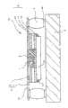
BGA型的半导体装置20,构成内插器基板3的绝缘基板1的焊球8(半导体元件4的外侧的焊球8)搭载部向着印刷配线板9一侧(半导体元件4的非接合面)进行约180°的弯曲,形成可折叠部1a。In the BGA
绝缘基板1的未弯曲部分和弯曲部分相对,以含有空隙22。由此,在可以缓和应力的同时,还有提高空间效率的效果和焊球8的缩小化的效果。The unbent portion and the bent portion of the insulating
空隙22中,如图3的右半部分所示,可以填满阻焊剂。也可以使用应力缓和弹性物或代替弹性物的连接层等作为添加物,来代替阻焊剂。由此,在可折叠部的固定化、尺寸精度、平衡度等方面可以得到有利的效果。The void 22 may be filled with solder resist as shown in the right half of FIG. 3 . Instead of the solder resist, a stress-relieving elastic material or a connection layer instead of the elastic material may be used as an additive. Thereby, advantageous effects can be obtained in terms of immobilization of the foldable portion, dimensional accuracy, balance, and the like.
在本实施方式中,除了像图3所示那样,作为外部端子的焊球8在半导体4的外侧(Fan-Out型)以外,还可以适用于焊球8同时在半导体元件4的下面和外侧这种情况(Fan-In/Out型)。In this embodiment, as shown in FIG. 3 , in addition to the
在图3和图4中,虽然图示省略,但配线图案2是导电性地与焊球8连接(在以下说明的作为第2~6的实施方式的说明图中的图5~14中,情况相同)。In FIG. 3 and FIG. 4, although illustration is omitted, the wiring pattern 2 is electrically connected to the solder ball 8 (in FIGS. , the same situation).
本实施方式的效果Effects of this embodiment
(1)由于在绝缘基板1的焊球搭载部上设有可折叠部1a,所以能够缓和半导体装置20与印刷配线板9(母板)之间产生的应力以及层叠型半导体装置20的半导体装置20之间产生的应力。(1) Since the foldable portion 1a is provided on the solder ball mounting portion of the insulating
(2)半导体装置20层叠时,可以弹性地调整上下半导体装置20的间隔。而且,还可实现焊球等的多榫化。(2) When the
本发明的第2实施方式The second embodiment of the present invention
半导体装置的结构Structure of Semiconductor Device
图5是表示本发明的第2实施方式所涉及的半导体装置的结构的说明图,图6是表示其层叠型半导体装置结构的说明图。除以下说明的事项以外,与第1实施方式所涉及的半导体装置和层叠型半导体装置相同。5 is an explanatory diagram showing the structure of a semiconductor device according to a second embodiment of the present invention, and FIG. 6 is an explanatory diagram showing the structure of the stacked semiconductor device. Except for the matters described below, it is the same as the semiconductor device and the stacked semiconductor device according to the first embodiment.
即,第1实施方式所涉及的半导体装置20的半导体元件4接合在与相对印刷配线板9的面为相反的面上,而本实施方式所涉及的半导体装置30的半导体元件4,接合于相对印刷配线板9的面上,这一点是不同的。That is, while the
可折叠部1a,是构成内插器基板3的绝缘基板1的焊球8(半导体元件4的外侧的焊球8)搭载部向着印刷配线板9一侧(半导体元件4的接合面一侧)弯曲约180°来形成的。The foldable portion 1a is a mounting portion facing the printed
在本实施方式中,适用于图5所示的,作为外部端子的焊球8在半导体元件4的外侧(Fan-Out型)的情况。This embodiment is applied to the case where the
本发明的第3实施方式The third embodiment of the present invention
半导体装置的结构Structure of Semiconductor Device
图7是表示本发明的第3实施方式所涉及的半导体装置的结构的说明图,图8是表示其层叠型半导体装置的结构的说明图。除以下说明的事项以外,与图1、2所示的半导体装置和层叠型半导体装置相同。连接层5不限于代替弹性物的连接层,也可以使用以往的应力缓和弹性物的结构。而且,可以不设置缓和层而只用接合层。7 is an explanatory diagram showing the structure of a semiconductor device according to a third embodiment of the present invention, and FIG. 8 is an explanatory diagram showing the structure of the stacked semiconductor device. Except for the matters described below, it is the same as the semiconductor device and the stacked semiconductor device shown in FIGS. 1 and 2 . The
BGA型的半导体装置40中,构成内插器基板3的绝缘基板1的焊球8(半导体元件4的外侧的焊球8)搭载部在半导体元件4的接合部(搭载部)的下方向(图7左半部分的结构)或上方向(图7的右半部分的结构)形成了成为阶梯状的段差部41a、41b。In the BGA type semiconductor device 40, the solder ball 8 (
焊球搭载部和半导体元件4搭载部可以不在同一平面上,希望其高低差(段差)在内插器基板的厚度以上,在该封装的高度以下。The solder ball mounting portion and the
在本实施方式中,除了像图7所示的,作为外部端子的焊球8在半导体元件4的外侧情况(Fan-Out型)外,焊球8还适用于同时在半导体元件4的下面和外侧(Fan-In/Out型)。In this embodiment, in addition to the case where the
本实施方式的效果Effects of this embodiment
(1)由于焊球8搭载部和半导体元件4搭载部具有阶梯状的段差部41a、41b,所以能够缓和半导体装置40与印刷配线板9(母板)之间产生的应力,以及层叠型半导体400的半导体装置40间产生的应力。(1) Since the
本发明的第4实施方式Fourth embodiment of the present invention
半导体装置的结构Structure of Semiconductor Device
图9是表示本发明的第4实施方式所涉及的半导体装置的结构的说明图,图10是表示其层叠型半导体装置的结构的说明图。除以下说明的事项以外,与第3实施方式所涉及的半导体装置和层叠型半导体装置相同。9 is an explanatory diagram showing the structure of a semiconductor device according to a fourth embodiment of the present invention, and FIG. 10 is an explanatory diagram showing the structure of the stacked semiconductor device. Except for the matters described below, it is the same as the semiconductor device and the stacked semiconductor device according to the third embodiment.
即,第3实施方式所涉及的半导体装置40的半导体元件4接合在与印刷配线板9相对的面为相反的面,本实施方式所涉及的半导体装置50的半导体元件4,接合于相对印刷配线板9的面上,这一点是不同的。That is, the
在本实施方式中,适用于如图9所示的,作为外部端子的焊球8在半导体元件4的外侧的情况(Fan-Out型)。In this embodiment, as shown in FIG. 9 , the
本发明的第5实施方式Fifth embodiment of the present invention
半导体装置的结构Structure of Semiconductor Device
图11是表示本发明的第5实施方式所涉及的半导体装置结构的说明图,图12是表示其层叠型半导体装置的结构的说明图。除以下说明的事项以外,与图1、2所示的半导体装置和层叠型半导体装置相同。连接层5不限于代替弹性物的连接层,可以使用以往的应力缓和弹性物的结构。而且,还可以是不设置缓和层只设有接合层。FIG. 11 is an explanatory diagram showing the structure of a semiconductor device according to a fifth embodiment of the present invention, and FIG. 12 is an explanatory diagram showing the structure of the stacked semiconductor device. Except for the matters described below, it is the same as the semiconductor device and the stacked semiconductor device shown in FIGS. 1 and 2 . The
BGA型的半导体装置60是在比半导体元件4的接合部(搭载部)的更靠外一侧,例如半导体元件4搭载部和焊球8(半导体元件4的外侧的焊球8)搭载部之间,用冲床或激光等在绝缘基板1上形成狭缝61。在狭缝61上,设计成部分地配置配线图案2。The BGA-
在狭缝61上,可以填充缓冲材料、其他的塑料等。The
狭缝61希望是宽1μm~1mm,长100μm~封装全长。对形状的细节在后面有叙述。The
在本实施方式中,除了像图11所示的,作为外部端子的焊球8在半导体元件4外侧(Fan-Out型)的情况,也适用于焊球8同时在半导体元件4的下面和外侧(Fan-In/Out型)。In this embodiment, in addition to the case where the
本实施方式的效果Effects of this embodiment
(1)因为在比半导体元件4搭载部的更靠外一侧(这里,是焊球8搭载部和半导体4搭载部之间),形成狭缝61,所以可以缓和半导体装置60与印刷配线板9(母板)之间产生的应力,以及层叠型半导体装置600的半导体装置60之间产生的应力。(1) Since the
本发明的第6实施方式Sixth embodiment of the present invention
半导体装置的结构Structure of Semiconductor Device
图13是表示本发明第6实施方式所涉及的半导体装置的结构的说明图,图14是表示其层叠型半导体装置的结构的说明图。除以下说明的事项以外,与第5实施方式所涉及的半导体装置和层叠型半导体装置相同。13 is an explanatory diagram showing the structure of a semiconductor device according to a sixth embodiment of the present invention, and FIG. 14 is an explanatory diagram showing the structure of the stacked semiconductor device. Except for the matters described below, it is the same as the semiconductor device and the stacked semiconductor device according to the fifth embodiment.
即,第5实施方式所涉及的半导体装置60的半导体元件4接合在与印刷配线板9相对的面为相反的面,而本实施方式所涉及的半导体装置70的半导体元件4,接合于相对印刷配线板9的面上,这一点是不同的。That is, while the
在本实施方式中,适用于图13所示的,作为外部端子的焊球8在半导体元件4的外侧的情况(Fan-Out型)。This embodiment is applied to the case (Fan-Out type) in which the
狭缝形状Slit shape
上述第5、第6实施方式所涉及的半导体装置和层叠型半导体装置中,狭缝61按以下说明,可取得各种形状。In the semiconductor device and the stacked semiconductor device according to the above-mentioned fifth and sixth embodiments, the
图15~图18例示出本发明第5、第6实施方式所涉及的半导体装置和层叠型半导体装置的绝缘基板1上所形成的狭缝61的形状。15 to 18 illustrate the shapes of the
图15的狭缝61a,与位于图中央的半导体元件4搭载部的长边平行,完全分离半导体元件4搭载侧和焊球8的焊接/接触侧。另一方面,狭缝61b,61c与半导体元件4搭载部的长边平行,不完全分离半导体元件4搭载侧和焊球8的焊接/接触侧(狭缝61b是长方形的窗口形状,狭缝61c是一端分离的梳齿状)。The
即,狭缝61a~61c与位于图中央的半导体元件4搭载部的长边平行,将半导体元件4搭载部和半导体4的外侧所配置的焊球8的搭载部完全或部分地分离。That is, the
图16的狭缝61d与位于图中央的半导体元件4搭载部的长边(或者短边)成直角,在半导体元件4搭载部的外侧,梳齿状地分离焊球8的焊接/接触区域。而且,狭缝61e是长方形的窗口形状,与半导体元件4搭载部的长边(或者短边)成直角,在半导体元件4搭载部的外侧,分离焊球8的焊接/接触区域。The
即,狭缝61d、61e与位于图中央的半导体元件4搭载部的长边或者短边相垂直,完全或部分地分离半导体元件4搭载部和在半导体元件4的外侧上配置的焊球8的搭载部。That is, the
图17表示复合方式,其具有图15和图16中表示的狭缝61a~61e的全部方式。FIG. 17 shows a composite form that has all the
图18的狭缝61f与位于图中央的半导体元件4搭载部的短边平行,完全分离半导体元件4搭载侧和焊球8的焊接/接触侧。另一方面,狭缝61g与半导体元件4搭载部的短边平行,不完全分离半导体元件4搭载侧和焊球8的焊接/接触侧(狭缝61g是长方形的窗口状)。The
即,狭缝61f、61g与位于图中央的半导体元件4搭载部的短边平行,完全或部分地分离半导体元件4搭载部和在半导体元件4的外侧上配置的焊球8的搭载部。That is, the
代替弹性物的连接层5的方式The method of replacing the
与所述的说明有一部分重复,但代替弹性物的连接层5的获取方式是如下所述。Part of the above description is repeated, but the method of obtaining the connecting
(1)连接层5具有由生成破坏、偏移(滑动)或剥离的材质构成的层,或者具有产生破坏、偏移(滑动)或剥离的结构,此破坏、偏移(滑动)或剥离产生于半导体元件4和连接层5的接合界面的一部分、内插器基板3和连接层5的接合界面的一部分或者连接层5内的层间界面的一部分,是由于半导体元件4和内插器基板3之间的应力作用而产生。(1) The
(2)连接层5具有由在半导体元件4和内插器基板3不分离的范围内该连接层5内部的一部分产生破坏或偏移(滑动)的材质来构成的层,或者,具有产生破坏或偏移(滑动)的结构,此破坏或偏移(滑动)是由于半导体元件4和内插器基板3之间的应力作用而产生。(2) The
(3)半导体元件4和内插器基板3通过树脂保持部分或整体以使其不分离,并且,连接层5具有由生成破坏、偏移(滑动)或剥离的材质构成的层,或者具有产生破坏、偏移(滑动)或剥离的结构,此破坏、偏移(滑动)或剥离产生于半导体元件4和连接层5的接合界面、内插器基板3和连接层5的接合界面或者连接层5内的层间界面,是由于半导体元件4和内插器基板3之间的应力作用而产生。(3) The
(4)半导体元件4和内插器基板3通过树脂保持部分或整体,以使其不分离,并且,连接层5具有由在该连接层5内部产生破坏或偏移(滑动)的材质构成的层,或者,具有产生破坏或偏移(滑动)的结构,是由于半导体元件4和内插器基板3之间的应力作用而产生。(4) The
(5)连接层5具有由带(薄膜)或糊剂构成的层。(5) The
(6)连接层5是含有芯层11和接合层12、13来构成的,该接合层用于将芯层11接合于半导体元件4和内插器基板3。(6) The
(7)连接层5由单层或2层的接合层构成。(7) The
(8)连接层5由具有2层以上的接合力的芯层构成。(8) The
(9)连接层5具有将光固化性物质(感光材料)薄膜化的干燥薄膜材料、内部具有液态层的带有机械结构的薄膜材料或者用Ag糊剂材料构成的层。(9) The
下面,更具体地说明代替弹性物的连接层5的获取方式。Next, the method of obtaining the connecting
单层连接层single connection layer
连接层5由单层的薄膜基材和沁入此基材的接合剂构成。将该接合剂的对于半导体元件4或内插器基板3的接合力设成1~500gf(0.01~5N)/mm2之间的比较弱的状态,使得在接合对象之间产生偏移(滑动)或剥离,来吸收应力。The
单层连接层single connection layer
连接层5是由包含树脂材料和装填物等填充材料的糊剂构成的。在0.01~5N/mm2以上的应力作用下,在树脂与填充材料的界面上的部分或全面地产生剥离等,或者在树脂材料内部(基体)部分或全面地产生裂纹、破裂等,来吸收应力。The
2层连接层2-layer connection layer
连接层5是将沁入上述接合剂的单层的薄膜基材以2张重合来制成2层结构。将该接合剂对于半导体元件4或内插器基板3的接合力调整成0.01~5N/mm2之间的比较弱的状态,使得在接合对象之间,或者2层的薄膜基材之间产生偏移(滑动)或剥离等,来吸收应力。The
2层连接层2-layer connection layer
连接层5是将沁入上述接合剂的单层的薄膜基材和与该薄膜基材接合力不同的薄膜基材进行2张重合来制成2层结构。将该接合剂的对于半导体元件4或内插器基板3的接合力调整成0.01~5N/mm2之间的比较弱的状态,使得在接合对象之间,或者2层的薄膜基材之间产生偏移(滑动)或剥离等,来吸收应力。The
3层连接层3 layers of connection layer
连接层5是将3张沁入上述接合剂的单层薄膜基材,或者2张该薄膜基材和1张与该薄膜基材的接合力不同的薄膜基材进行重合(不考虑重合顺序)制成3层结构。将该接合剂对于半导体元件4或内插器基板3的接合力调整成0.01~5N/mm2之间的比较弱的状态,使得在接合对象之间,或者同种或异种的薄膜基材之间产生偏移(滑动)或剥离等,来吸收应力。The
2层连接层(连接层的方向性的例子)2-layer connection layer (example of directionality of connection layer)
连接层5是将2张沁入上述接合剂的单层的薄膜基材(芯层11A,11B),或者1张该薄膜基材和1张与该薄膜基材的接合力不同的薄膜基材进行重合,制成2层结构(将对半导体元件4或内插器基板3的接合力调整成0.01~5N/mm2之间的比较弱的状态),各层在剥离或分裂强度上具有方向性(例如,X方向上强,Y方向上弱)。例如,90度转向重合同种的2张薄膜基材,使得有意地产生各层的剥离、分裂等,吸收施加于半导体元件4上的来自于360度任一XY面的应力。而且,上下2层的接合层的方向的改变可以在45~135度的范围。The
3层以上连接层(用芯层吸收的例子)3 or more connection layers (example of absorbing with core layer)
连接层5是将3张以上沁入上述接合剂的单层的薄膜基材(芯层11A、11B),或者2张该薄膜基材和1张以上与该薄膜基材的接合力不同的薄膜基材进行重合,制成3层以上的结构(将对半导体元件4或内插器基板3的接合力调整成0.01~5N/mm2之间的比较弱的状态),各层在剥离或分裂强度上具有方向性(例如,X方向上强,Y方向上弱)。例如,以90度转向来重合同种的2张薄膜基材(芯层11A),将与芯层11A不同的同种的2张的薄膜基材(芯层11B)进行90度转向来夹住芯层11A从而进行重合,通过产生各层的剥离,分裂等,来吸收施加于半导体元件4上的来自于360度任一XY面的应力。而且,同种的上下2层的接合层的方向的改变,可以在45~135度的范围。The
在上述具体例子中,例举了将芯层沁入接合剂的方式,但在这些具体例子中,也可以采用将具有接合力的接合层以其他的方法设置于单侧或两侧的方式。In the above-mentioned specific examples, the method of impregnating the core layer with the bonding agent was exemplified, but in these specific examples, the method of providing the bonding layer having bonding force on one side or both sides by other methods may also be adopted.
接合强度的调整Adjustment of bonding strength
在下面,例示出调整连接层5的接合力的方法。In the following, a method of adjusting the bonding force of the
(1)减少糊剂基材的量,增多与装填物等的直接接合性无关的部分的比例,使得连接层内部的以及与接合对象的接合面积减少,来抑制接合强度使其变低。(1) Reduce the amount of the paste base material and increase the ratio of the portion not related to the direct bondability of the filler, etc., so that the bonding area inside the connection layer and the bonding object is reduced, and the bonding strength is suppressed to be low.
(2)通过将接合剂不均匀(不均一)地沁入,可以实现接合强度的变更(0~100%)。(2) The bonding strength can be changed (0 to 100%) by unevenly (non-uniformly) impregnating the bonding agent.
(3)部分地沁入接合剂,使得连接层内部的以及与接合对象的接合面积减少,来抑制接合强度使其变低。(3) Partial penetration of the bonding agent reduces the bonding area inside the connection layer and with the bonding object, thereby suppressing the bonding strength from becoming low.
(4)具有2层以上的芯层时,变更各层沁入的接合剂,将接合层之间的接合强度调整得比接合层与接合对象的接合强度低,使得接合层间可以先产生偏移(滑动)或剥离等。(4) When there are two or more core layers, change the bonding agent in each layer, and adjust the bonding strength between the bonding layers to be lower than the bonding strength between the bonding layer and the bonding object, so that the gap between the bonding layers can be generated first. Move (slide) or peel off, etc.
代替弹性物的连接层5的效果Effect of connecting
利用使用代替弹性物的连接层5的实施方式,获得以下效果。With the embodiment using the
(1)通过采用在半导体元件和内插器基板之间的应力起作用时,产生破坏、偏移(滑动)或剥离的材质构成的连接层,或者通过使用具有产生破坏、偏移(滑动)或剥离的结构的连接层,能得到缓和该应力的半导体装置。这里,缓和是指吸收、分散等。(1) By using a connection layer made of a material that causes damage, deflection (slip) or peeling when stress acts between the semiconductor element and the interposer substrate, or by using a material that causes damage, deflection (slide) Or the connection layer of the structure peeled off can obtain the semiconductor device which relaxes this stress. Here, moderation refers to absorption, dispersion, and the like.
(2)因为不需要使用以往的应力缓和弹性物,所以在构成半导体装置及内插器基板的方面,能够降低材料价格,而且,与以往的应力缓和弹性物相比,其获取也容易。(2) Since there is no need to use conventional stress relieving elastic materials, material costs can be reduced in constituting semiconductor devices and interposer substrates, and they are also easier to obtain than conventional stress relieving elastic materials.
本发明的其他的实施方式Other embodiments of the present invention
本发明不限于上述各实施方式,可以在不脱离或变更本发明的技术思想的范围内进行种种变形。The present invention is not limited to the above-described embodiments, and various modifications can be made without departing from or changing the technical idea of the present invention.
例如,在上述实施方式中,以BGA型为例,进行说明,但也适用于产生同样问题的半导体装置,例如CSP型或SIP型的半导体装置。而且,也可适用于MCP(多芯片封装)。For example, in the above-mentioned embodiment, the BGA type is taken as an example for description, but it is also applicable to a semiconductor device having the same problem, such as a CSP type or a SIP type semiconductor device. Furthermore, it is also applicable to MCP (Multi-Chip Package).
Claims (6)
Applications Claiming Priority (3)
| Application Number | Priority Date | Filing Date | Title |
|---|---|---|---|
| JP2006311850 | 2006-11-17 | ||
| JP2006311850AJP5028968B2 (en) | 2006-11-17 | 2006-11-17 | Semiconductor device, stacked semiconductor device, and interposer substrate |
| JP2006-311850 | 2006-11-17 |
Related Child Applications (2)
| Application Number | Title | Priority Date | Filing Date |
|---|---|---|---|
| CN2009101498776ADivisionCN101604678B (en) | 2006-11-17 | 2007-11-16 | Semiconductor device, stacked semiconductor device, and interposer substrate |
| CN2009101498780ADivisionCN101604681B (en) | 2006-11-17 | 2007-11-16 | Semiconductor device, stacked semiconductor device and interposer substrate |
Publications (2)
| Publication Number | Publication Date |
|---|---|
| CN101183670A CN101183670A (en) | 2008-05-21 |
| CN101183670Btrue CN101183670B (en) | 2011-06-22 |
Family
ID=39416112
Family Applications (3)
| Application Number | Title | Priority Date | Filing Date |
|---|---|---|---|
| CN2007101927202AExpired - Fee RelatedCN101183670B (en) | 2006-11-17 | 2007-11-16 | Semiconductor device, stacked semiconductor device, and interposer substrate |
| CN2009101498776AExpired - Fee RelatedCN101604678B (en) | 2006-11-17 | 2007-11-16 | Semiconductor device, stacked semiconductor device, and interposer substrate |
| CN2009101498780AExpired - Fee RelatedCN101604681B (en) | 2006-11-17 | 2007-11-16 | Semiconductor device, stacked semiconductor device and interposer substrate |
Family Applications After (2)
| Application Number | Title | Priority Date | Filing Date |
|---|---|---|---|
| CN2009101498776AExpired - Fee RelatedCN101604678B (en) | 2006-11-17 | 2007-11-16 | Semiconductor device, stacked semiconductor device, and interposer substrate |
| CN2009101498780AExpired - Fee RelatedCN101604681B (en) | 2006-11-17 | 2007-11-16 | Semiconductor device, stacked semiconductor device and interposer substrate |
Country Status (5)
| Country | Link |
|---|---|
| US (2) | US20080116559A1 (en) |
| JP (1) | JP5028968B2 (en) |
| KR (1) | KR100892203B1 (en) |
| CN (3) | CN101183670B (en) |
| TW (1) | TW200832659A (en) |
Families Citing this family (9)
| Publication number | Priority date | Publication date | Assignee | Title |
|---|---|---|---|---|
| JP5671681B2 (en)* | 2009-03-05 | 2015-02-18 | ピーエスフォー ルクスコ エスエイアールエルPS4 Luxco S.a.r.l. | Multilayer semiconductor device |
| US8363418B2 (en) | 2011-04-18 | 2013-01-29 | Morgan/Weiss Technologies Inc. | Above motherboard interposer with peripheral circuits |
| JP6594556B1 (en)* | 2018-01-17 | 2019-10-23 | 新電元工業株式会社 | Electronic module |
| KR102743244B1 (en)* | 2019-02-12 | 2024-12-18 | 삼성전자주식회사 | Printed circuit board and semconductor package including the same |
| JP7135999B2 (en)* | 2019-05-13 | 2022-09-13 | 株式会社オートネットワーク技術研究所 | wiring board |
| JP7156230B2 (en)* | 2019-10-02 | 2022-10-19 | 株式会社デンソー | semiconductor module |
| IT202000001819A1 (en) | 2020-01-30 | 2021-07-30 | St Microelectronics Srl | INTEGRATED CIRCUIT AND ELECTRONIC DEVICE INCLUDING A PLURALITY OF INTEGRATED CIRCUITS ELECTRICALLY COUPLED VIA A SYNCHRONIZATION SIGNAL |
| CN112588222B (en)* | 2020-11-25 | 2022-02-18 | 浙江大学 | Porous polymer preparation device and method with surface acoustic wave regulating porosity and arrangement |
| WO2024232169A1 (en)* | 2023-05-09 | 2024-11-14 | ソニーグループ株式会社 | Relay member and electronic apparatus |
Citations (2)
| Publication number | Priority date | Publication date | Assignee | Title |
|---|---|---|---|---|
| US6160308A (en)* | 1999-03-10 | 2000-12-12 | Kabushiki Kaisha Toshiba | Semiconductor device |
| CN1343007A (en)* | 2000-09-05 | 2002-04-03 | 精工爱普生株式会社 | Semiconductor device, manufacturing method, thereof, circuit base plate and electronic equipment |
Family Cites Families (21)
| Publication number | Priority date | Publication date | Assignee | Title |
|---|---|---|---|---|
| US6111306A (en)* | 1993-12-06 | 2000-08-29 | Fujitsu Limited | Semiconductor device and method of producing the same and semiconductor device unit and method of producing the same |
| JPH07201912A (en)* | 1993-12-28 | 1995-08-04 | Hitachi Cable Ltd | Film carrier type semiconductor device and film carrier |
| JPH0831868A (en)* | 1994-07-21 | 1996-02-02 | Hitachi Cable Ltd | BGA type semiconductor device |
| US5747874A (en)* | 1994-09-20 | 1998-05-05 | Fujitsu Limited | Semiconductor device, base member for semiconductor device and semiconductor device unit |
| JP2755252B2 (en)* | 1996-05-30 | 1998-05-20 | 日本電気株式会社 | Semiconductor device package and semiconductor device |
| JP3195236B2 (en)* | 1996-05-30 | 2001-08-06 | 株式会社日立製作所 | Wiring tape having adhesive film, semiconductor device and manufacturing method |
| US6617193B1 (en)* | 1997-04-30 | 2003-09-09 | Hitachi Chemical Company, Ltd. | Semiconductor device, semiconductor device substrate, and methods of fabricating the same |
| JP2924854B2 (en)* | 1997-05-20 | 1999-07-26 | 日本電気株式会社 | Semiconductor device and manufacturing method thereof |
| JP3639088B2 (en)* | 1997-06-06 | 2005-04-13 | 株式会社ルネサステクノロジ | Semiconductor device and wiring tape |
| US6300679B1 (en)* | 1998-06-01 | 2001-10-09 | Semiconductor Components Industries, Llc | Flexible substrate for packaging a semiconductor component |
| JP2000077563A (en)* | 1998-08-31 | 2000-03-14 | Sharp Corp | Semiconductor device and method of manufacturing the same |
| JP3180800B2 (en) | 1999-04-08 | 2001-06-25 | カシオ計算機株式会社 | Semiconductor device and manufacturing method thereof |
| JP2002289741A (en)* | 2001-03-23 | 2002-10-04 | Nec Kyushu Ltd | Semiconductor device |
| JP4103342B2 (en)* | 2001-05-22 | 2008-06-18 | 日立電線株式会社 | Manufacturing method of semiconductor device |
| JP3705235B2 (en)* | 2002-04-16 | 2005-10-12 | 日立電線株式会社 | Manufacturing method of semiconductor device |
| JP4225036B2 (en) | 2002-11-20 | 2009-02-18 | 日本電気株式会社 | Semiconductor package and stacked semiconductor package |
| JP3900093B2 (en)* | 2003-03-11 | 2007-04-04 | 日立電線株式会社 | Mold and method for manufacturing semiconductor device using the same |
| TW200514484A (en)* | 2003-10-08 | 2005-04-16 | Chung-Cheng Wang | Substrate for electrical device and methods of fabricating the same |
| JP4291209B2 (en)* | 2004-05-20 | 2009-07-08 | エルピーダメモリ株式会社 | Manufacturing method of semiconductor device |
| US7154175B2 (en)* | 2004-06-21 | 2006-12-26 | Intel Corporation | Ground plane for integrated circuit package |
| KR100715316B1 (en)* | 2006-02-13 | 2007-05-08 | 삼성전자주식회사 | Semiconductor chip package mounting structure using flexible circuit board |
- 2006
- 2006-11-17JPJP2006311850Apatent/JP5028968B2/ennot_activeExpired - Fee Related
- 2007
- 2007-10-16TWTW096138590Apatent/TW200832659A/ennot_activeIP Right Cessation
- 2007-11-08USUS11/979,785patent/US20080116559A1/ennot_activeAbandoned
- 2007-11-16KRKR1020070117566Apatent/KR100892203B1/ennot_activeExpired - Fee Related
- 2007-11-16CNCN2007101927202Apatent/CN101183670B/ennot_activeExpired - Fee Related
- 2007-11-16CNCN2009101498776Apatent/CN101604678B/ennot_activeExpired - Fee Related
- 2007-11-16CNCN2009101498780Apatent/CN101604681B/ennot_activeExpired - Fee Related
- 2010
- 2010-03-16USUS12/725,090patent/US20100171210A1/ennot_activeAbandoned
Patent Citations (2)
| Publication number | Priority date | Publication date | Assignee | Title |
|---|---|---|---|---|
| US6160308A (en)* | 1999-03-10 | 2000-12-12 | Kabushiki Kaisha Toshiba | Semiconductor device |
| CN1343007A (en)* | 2000-09-05 | 2002-04-03 | 精工爱普生株式会社 | Semiconductor device, manufacturing method, thereof, circuit base plate and electronic equipment |
Also Published As
| Publication number | Publication date |
|---|---|
| KR20080045079A (en) | 2008-05-22 |
| CN101604681A (en) | 2009-12-16 |
| JP5028968B2 (en) | 2012-09-19 |
| US20100171210A1 (en) | 2010-07-08 |
| TW200832659A (en) | 2008-08-01 |
| CN101604678B (en) | 2012-02-22 |
| KR100892203B1 (en) | 2009-04-07 |
| US20080116559A1 (en) | 2008-05-22 |
| CN101604681B (en) | 2012-03-14 |
| JP2008130678A (en) | 2008-06-05 |
| CN101183670A (en) | 2008-05-21 |
| CN101604678A (en) | 2009-12-16 |
| TWI363412B (en) | 2012-05-01 |
Similar Documents
| Publication | Publication Date | Title |
|---|---|---|
| CN101183670B (en) | Semiconductor device, stacked semiconductor device, and interposer substrate | |
| CN1812088B (en) | Multi-level semiconductor module and method for fabricating the same | |
| JP4830120B2 (en) | Electronic package and manufacturing method thereof | |
| US20060087020A1 (en) | Semiconductor device and method for producing the same | |
| JP5075463B2 (en) | Semiconductor device | |
| JPH10294423A (en) | Semiconductor device | |
| JP2009141169A (en) | Semiconductor device | |
| KR20100009941A (en) | Semiconductor package having stepped molding compound with conductive via, method for formation of the same and stacked semiconductor package using the same | |
| CN1638120A (en) | Semiconductor-mounted device and method for producing same | |
| KR20100032452A (en) | Device having electronic component mounted therein and method for manufacturing such device | |
| CN101872757A (en) | Cavity chip package structure and package-on-package structure using the same | |
| US20080185709A1 (en) | Semiconductor device including semiconductor elements and method of producing semiconductor device | |
| CN101809740B (en) | Electronic component mounting structure and manufacturing method thereof | |
| JP2009238854A (en) | Mounting structure of semiconductor device, and electronic apparatus using mounting structure | |
| KR100441382B1 (en) | Semiconductor device and manufacturing method of the same | |
| CN107180807A (en) | Semiconductor device and its manufacture method | |
| JP2005303267A (en) | Multilayer electronic components | |
| JP2008311508A (en) | Electronic component package and manufacturing method thereof | |
| JP4480710B2 (en) | Semiconductor device embedded substrate | |
| JP2002289735A (en) | Semiconductor device | |
| JP2007227608A (en) | Semiconductor device and manufacturing method of semiconductor device | |
| JP2007067053A (en) | Component built-in module and manufacturing method thereof | |
| JP2018207015A (en) | Electronic device, method for manufacturing electronic device, and electronic apparatus | |
| JP2002373966A (en) | Semiconductor chip mounting structure and method of manufacturing the same | |
| JP2003037244A (en) | Semiconductor device tape carrier and semiconductor device using the same |
Legal Events
| Date | Code | Title | Description |
|---|---|---|---|
| C06 | Publication | ||
| PB01 | Publication | ||
| C10 | Entry into substantive examination | ||
| SE01 | Entry into force of request for substantive examination | ||
| C14 | Grant of patent or utility model | ||
| GR01 | Patent grant | ||
| C17 | Cessation of patent right | ||
| CF01 | Termination of patent right due to non-payment of annual fee | Granted publication date:20110622 Termination date:20131116 |