CN101183668B - Semiconductor device having projecting electrode formed by electrolytic plating, and manufacturing method thereof - Google Patents
Semiconductor device having projecting electrode formed by electrolytic plating, and manufacturing method thereofDownload PDFInfo
- Publication number
- CN101183668B CN101183668BCN2007101596981ACN200710159698ACN101183668BCN 101183668 BCN101183668 BCN 101183668BCN 2007101596981 ACN2007101596981 ACN 2007101596981ACN 200710159698 ACN200710159698 ACN 200710159698ACN 101183668 BCN101183668 BCN 101183668B
- Authority
- CN
- China
- Prior art keywords
- mentioned
- metal layer
- protection film
- semiconductor device
- wiring
- Prior art date
- Legal status (The legal status is an assumption and is not a legal conclusion. Google has not performed a legal analysis and makes no representation as to the accuracy of the status listed.)
- Active
Links
- 239000004065semiconductorSubstances0.000titleclaimsabstractdescription57
- 238000004519manufacturing processMethods0.000titleclaimsabstractdescription23
- 238000009713electroplatingMethods0.000titleabstractdescription21
- 229910052751metalInorganic materials0.000claimsabstractdescription54
- 239000002184metalSubstances0.000claimsabstractdescription54
- ATJFFYVFTNAWJD-UHFFFAOYSA-NTinChemical compound[Sn]ATJFFYVFTNAWJD-UHFFFAOYSA-N0.000claimsdescription17
- 239000000758substrateSubstances0.000claimsdescription15
- 230000001681protective effectEffects0.000abstractdescription53
- 238000007747platingMethods0.000abstractdescription34
- 238000000034methodMethods0.000abstractdescription16
- RYGMFSIKBFXOCR-UHFFFAOYSA-NCopperChemical compound[Cu]RYGMFSIKBFXOCR-UHFFFAOYSA-N0.000abstractdescription13
- 229910052802copperInorganic materials0.000abstractdescription13
- 239000010949copperSubstances0.000abstractdescription13
- 230000015572biosynthetic processEffects0.000abstractdescription12
- 229920001721polyimidePolymers0.000abstractdescription5
- 239000009719polyimide resinSubstances0.000abstractdescription4
- 239000010408filmSubstances0.000description96
- 239000010410layerSubstances0.000description56
- 229910000679solderInorganic materials0.000description23
- PXHVJJICTQNCMI-UHFFFAOYSA-NNickelChemical compound[Ni]PXHVJJICTQNCMI-UHFFFAOYSA-N0.000description4
- XUIMIQQOPSSXEZ-UHFFFAOYSA-NSiliconChemical compound[Si]XUIMIQQOPSSXEZ-UHFFFAOYSA-N0.000description4
- 230000004907fluxEffects0.000description4
- 229910052710siliconInorganic materials0.000description4
- 239000010703siliconSubstances0.000description4
- 238000004544sputter depositionMethods0.000description4
- 238000005530etchingMethods0.000description3
- VYPSYNLAJGMNEJ-UHFFFAOYSA-NSilicium dioxideChemical compoundO=[Si]=OVYPSYNLAJGMNEJ-UHFFFAOYSA-N0.000description2
- 229910052782aluminiumInorganic materials0.000description2
- XAGFODPZIPBFFR-UHFFFAOYSA-NaluminiumChemical compound[Al]XAGFODPZIPBFFR-UHFFFAOYSA-N0.000description2
- PCHJSUWPFVWCPO-UHFFFAOYSA-NgoldChemical compound[Au]PCHJSUWPFVWCPO-UHFFFAOYSA-N0.000description2
- 229910052737goldInorganic materials0.000description2
- 239000010931goldSubstances0.000description2
- 229910052759nickelInorganic materials0.000description2
- 238000000206photolithographyMethods0.000description2
- 229910052814silicon oxideInorganic materials0.000description2
- 238000004528spin coatingMethods0.000description2
- 239000002335surface treatment layerSubstances0.000description2
- 239000004642PolyimideSubstances0.000description1
- RTAQQCXQSZGOHL-UHFFFAOYSA-NTitaniumChemical compound[Ti]RTAQQCXQSZGOHL-UHFFFAOYSA-N0.000description1
- 150000001412aminesChemical class0.000description1
- 239000011248coating agentSubstances0.000description1
- 238000000576coating methodMethods0.000description1
- 238000007796conventional methodMethods0.000description1
- 230000007547defectEffects0.000description1
- 238000007772electroless platingMethods0.000description1
- 238000000227grindingMethods0.000description1
- 238000009413insulationMethods0.000description1
- 239000007788liquidSubstances0.000description1
- 230000002093peripheral effectEffects0.000description1
- 239000011347resinSubstances0.000description1
- 229920005989resinPolymers0.000description1
- 238000007650screen-printingMethods0.000description1
- 238000007789sealingMethods0.000description1
- 239000010409thin filmSubstances0.000description1
- 239000010936titaniumSubstances0.000description1
- 229910052719titaniumInorganic materials0.000description1
- 238000001721transfer mouldingMethods0.000description1
Images


Classifications
- H—ELECTRICITY
- H01—ELECTRIC ELEMENTS
- H01L—SEMICONDUCTOR DEVICES NOT COVERED BY CLASS H10
- H01L23/00—Details of semiconductor or other solid state devices
- H01L23/28—Encapsulations, e.g. encapsulating layers, coatings, e.g. for protection
- H01L23/31—Encapsulations, e.g. encapsulating layers, coatings, e.g. for protection characterised by the arrangement or shape
- H01L23/3107—Encapsulations, e.g. encapsulating layers, coatings, e.g. for protection characterised by the arrangement or shape the device being completely enclosed
- H01L23/3114—Encapsulations, e.g. encapsulating layers, coatings, e.g. for protection characterised by the arrangement or shape the device being completely enclosed the device being a chip scale package, e.g. CSP
- H—ELECTRICITY
- H01—ELECTRIC ELEMENTS
- H01L—SEMICONDUCTOR DEVICES NOT COVERED BY CLASS H10
- H01L23/00—Details of semiconductor or other solid state devices
- H01L23/12—Mountings, e.g. non-detachable insulating substrates
- H—ELECTRICITY
- H01—ELECTRIC ELEMENTS
- H01L—SEMICONDUCTOR DEVICES NOT COVERED BY CLASS H10
- H01L23/00—Details of semiconductor or other solid state devices
- H01L23/48—Arrangements for conducting electric current to or from the solid state body in operation, e.g. leads, terminal arrangements ; Selection of materials therefor
- H—ELECTRICITY
- H01—ELECTRIC ELEMENTS
- H01L—SEMICONDUCTOR DEVICES NOT COVERED BY CLASS H10
- H01L23/00—Details of semiconductor or other solid state devices
- H01L23/52—Arrangements for conducting electric current within the device in operation from one component to another, i.e. interconnections, e.g. wires, lead frames
- H—ELECTRICITY
- H01—ELECTRIC ELEMENTS
- H01L—SEMICONDUCTOR DEVICES NOT COVERED BY CLASS H10
- H01L24/00—Arrangements for connecting or disconnecting semiconductor or solid-state bodies; Methods or apparatus related thereto
- H01L24/01—Means for bonding being attached to, or being formed on, the surface to be connected, e.g. chip-to-package, die-attach, "first-level" interconnects; Manufacturing methods related thereto
- H01L24/10—Bump connectors ; Manufacturing methods related thereto
- H01L24/11—Manufacturing methods
- H—ELECTRICITY
- H01—ELECTRIC ELEMENTS
- H01L—SEMICONDUCTOR DEVICES NOT COVERED BY CLASS H10
- H01L24/00—Arrangements for connecting or disconnecting semiconductor or solid-state bodies; Methods or apparatus related thereto
- H01L24/01—Means for bonding being attached to, or being formed on, the surface to be connected, e.g. chip-to-package, die-attach, "first-level" interconnects; Manufacturing methods related thereto
- H01L24/10—Bump connectors ; Manufacturing methods related thereto
- H01L24/12—Structure, shape, material or disposition of the bump connectors prior to the connecting process
- H—ELECTRICITY
- H01—ELECTRIC ELEMENTS
- H01L—SEMICONDUCTOR DEVICES NOT COVERED BY CLASS H10
- H01L2224/00—Indexing scheme for arrangements for connecting or disconnecting semiconductor or solid-state bodies and methods related thereto as covered by H01L24/00
- H01L2224/01—Means for bonding being attached to, or being formed on, the surface to be connected, e.g. chip-to-package, die-attach, "first-level" interconnects; Manufacturing methods related thereto
- H01L2224/02—Bonding areas; Manufacturing methods related thereto
- H01L2224/023—Redistribution layers [RDL] for bonding areas
- H01L2224/0231—Manufacturing methods of the redistribution layers
- H01L2224/02311—Additive methods
- H—ELECTRICITY
- H01—ELECTRIC ELEMENTS
- H01L—SEMICONDUCTOR DEVICES NOT COVERED BY CLASS H10
- H01L2224/00—Indexing scheme for arrangements for connecting or disconnecting semiconductor or solid-state bodies and methods related thereto as covered by H01L24/00
- H01L2224/01—Means for bonding being attached to, or being formed on, the surface to be connected, e.g. chip-to-package, die-attach, "first-level" interconnects; Manufacturing methods related thereto
- H01L2224/02—Bonding areas; Manufacturing methods related thereto
- H01L2224/023—Redistribution layers [RDL] for bonding areas
- H01L2224/0231—Manufacturing methods of the redistribution layers
- H01L2224/02313—Subtractive methods
- H—ELECTRICITY
- H01—ELECTRIC ELEMENTS
- H01L—SEMICONDUCTOR DEVICES NOT COVERED BY CLASS H10
- H01L2224/00—Indexing scheme for arrangements for connecting or disconnecting semiconductor or solid-state bodies and methods related thereto as covered by H01L24/00
- H01L2224/01—Means for bonding being attached to, or being formed on, the surface to be connected, e.g. chip-to-package, die-attach, "first-level" interconnects; Manufacturing methods related thereto
- H01L2224/02—Bonding areas; Manufacturing methods related thereto
- H01L2224/03—Manufacturing methods
- H01L2224/0347—Manufacturing methods using a lift-off mask
- H—ELECTRICITY
- H01—ELECTRIC ELEMENTS
- H01L—SEMICONDUCTOR DEVICES NOT COVERED BY CLASS H10
- H01L2224/00—Indexing scheme for arrangements for connecting or disconnecting semiconductor or solid-state bodies and methods related thereto as covered by H01L24/00
- H01L2224/01—Means for bonding being attached to, or being formed on, the surface to be connected, e.g. chip-to-package, die-attach, "first-level" interconnects; Manufacturing methods related thereto
- H01L2224/02—Bonding areas; Manufacturing methods related thereto
- H01L2224/03—Manufacturing methods
- H01L2224/036—Manufacturing methods by patterning a pre-deposited material
- H01L2224/0361—Physical or chemical etching
- H—ELECTRICITY
- H01—ELECTRIC ELEMENTS
- H01L—SEMICONDUCTOR DEVICES NOT COVERED BY CLASS H10
- H01L2224/00—Indexing scheme for arrangements for connecting or disconnecting semiconductor or solid-state bodies and methods related thereto as covered by H01L24/00
- H01L2224/01—Means for bonding being attached to, or being formed on, the surface to be connected, e.g. chip-to-package, die-attach, "first-level" interconnects; Manufacturing methods related thereto
- H01L2224/02—Bonding areas; Manufacturing methods related thereto
- H01L2224/03—Manufacturing methods
- H01L2224/039—Methods of manufacturing bonding areas involving a specific sequence of method steps
- H01L2224/03912—Methods of manufacturing bonding areas involving a specific sequence of method steps the bump being used as a mask for patterning the bonding area
- H—ELECTRICITY
- H01—ELECTRIC ELEMENTS
- H01L—SEMICONDUCTOR DEVICES NOT COVERED BY CLASS H10
- H01L2224/00—Indexing scheme for arrangements for connecting or disconnecting semiconductor or solid-state bodies and methods related thereto as covered by H01L24/00
- H01L2224/01—Means for bonding being attached to, or being formed on, the surface to be connected, e.g. chip-to-package, die-attach, "first-level" interconnects; Manufacturing methods related thereto
- H01L2224/02—Bonding areas; Manufacturing methods related thereto
- H01L2224/04—Structure, shape, material or disposition of the bonding areas prior to the connecting process
- H01L2224/0401—Bonding areas specifically adapted for bump connectors, e.g. under bump metallisation [UBM]
- H—ELECTRICITY
- H01—ELECTRIC ELEMENTS
- H01L—SEMICONDUCTOR DEVICES NOT COVERED BY CLASS H10
- H01L2224/00—Indexing scheme for arrangements for connecting or disconnecting semiconductor or solid-state bodies and methods related thereto as covered by H01L24/00
- H01L2224/01—Means for bonding being attached to, or being formed on, the surface to be connected, e.g. chip-to-package, die-attach, "first-level" interconnects; Manufacturing methods related thereto
- H01L2224/10—Bump connectors; Manufacturing methods related thereto
- H01L2224/11—Manufacturing methods
- H01L2224/113—Manufacturing methods by local deposition of the material of the bump connector
- H01L2224/1131—Manufacturing methods by local deposition of the material of the bump connector in liquid form
- H01L2224/1132—Screen printing, i.e. using a stencil
- H—ELECTRICITY
- H01—ELECTRIC ELEMENTS
- H01L—SEMICONDUCTOR DEVICES NOT COVERED BY CLASS H10
- H01L2224/00—Indexing scheme for arrangements for connecting or disconnecting semiconductor or solid-state bodies and methods related thereto as covered by H01L24/00
- H01L2224/01—Means for bonding being attached to, or being formed on, the surface to be connected, e.g. chip-to-package, die-attach, "first-level" interconnects; Manufacturing methods related thereto
- H01L2224/10—Bump connectors; Manufacturing methods related thereto
- H01L2224/11—Manufacturing methods
- H01L2224/114—Manufacturing methods by blanket deposition of the material of the bump connector
- H01L2224/1146—Plating
- H01L2224/11462—Electroplating
- H—ELECTRICITY
- H01—ELECTRIC ELEMENTS
- H01L—SEMICONDUCTOR DEVICES NOT COVERED BY CLASS H10
- H01L2224/00—Indexing scheme for arrangements for connecting or disconnecting semiconductor or solid-state bodies and methods related thereto as covered by H01L24/00
- H01L2224/01—Means for bonding being attached to, or being formed on, the surface to be connected, e.g. chip-to-package, die-attach, "first-level" interconnects; Manufacturing methods related thereto
- H01L2224/10—Bump connectors; Manufacturing methods related thereto
- H01L2224/11—Manufacturing methods
- H01L2224/1147—Manufacturing methods using a lift-off mask
- H—ELECTRICITY
- H01—ELECTRIC ELEMENTS
- H01L—SEMICONDUCTOR DEVICES NOT COVERED BY CLASS H10
- H01L2224/00—Indexing scheme for arrangements for connecting or disconnecting semiconductor or solid-state bodies and methods related thereto as covered by H01L24/00
- H01L2224/01—Means for bonding being attached to, or being formed on, the surface to be connected, e.g. chip-to-package, die-attach, "first-level" interconnects; Manufacturing methods related thereto
- H01L2224/10—Bump connectors; Manufacturing methods related thereto
- H01L2224/11—Manufacturing methods
- H01L2224/118—Post-treatment of the bump connector
- H01L2224/11848—Thermal treatments, e.g. annealing, controlled cooling
- H01L2224/11849—Reflowing
- H—ELECTRICITY
- H01—ELECTRIC ELEMENTS
- H01L—SEMICONDUCTOR DEVICES NOT COVERED BY CLASS H10
- H01L2224/00—Indexing scheme for arrangements for connecting or disconnecting semiconductor or solid-state bodies and methods related thereto as covered by H01L24/00
- H01L2224/01—Means for bonding being attached to, or being formed on, the surface to be connected, e.g. chip-to-package, die-attach, "first-level" interconnects; Manufacturing methods related thereto
- H01L2224/10—Bump connectors; Manufacturing methods related thereto
- H01L2224/11—Manufacturing methods
- H01L2224/119—Methods of manufacturing bump connectors involving a specific sequence of method steps
- H01L2224/11901—Methods of manufacturing bump connectors involving a specific sequence of method steps with repetition of the same manufacturing step
- H—ELECTRICITY
- H01—ELECTRIC ELEMENTS
- H01L—SEMICONDUCTOR DEVICES NOT COVERED BY CLASS H10
- H01L2224/00—Indexing scheme for arrangements for connecting or disconnecting semiconductor or solid-state bodies and methods related thereto as covered by H01L24/00
- H01L2224/01—Means for bonding being attached to, or being formed on, the surface to be connected, e.g. chip-to-package, die-attach, "first-level" interconnects; Manufacturing methods related thereto
- H01L2224/10—Bump connectors; Manufacturing methods related thereto
- H01L2224/12—Structure, shape, material or disposition of the bump connectors prior to the connecting process
- H01L2224/13—Structure, shape, material or disposition of the bump connectors prior to the connecting process of an individual bump connector
- H01L2224/13001—Core members of the bump connector
- H01L2224/1302—Disposition
- H01L2224/13023—Disposition the whole bump connector protruding from the surface
- H—ELECTRICITY
- H01—ELECTRIC ELEMENTS
- H01L—SEMICONDUCTOR DEVICES NOT COVERED BY CLASS H10
- H01L2224/00—Indexing scheme for arrangements for connecting or disconnecting semiconductor or solid-state bodies and methods related thereto as covered by H01L24/00
- H01L2224/01—Means for bonding being attached to, or being formed on, the surface to be connected, e.g. chip-to-package, die-attach, "first-level" interconnects; Manufacturing methods related thereto
- H01L2224/10—Bump connectors; Manufacturing methods related thereto
- H01L2224/12—Structure, shape, material or disposition of the bump connectors prior to the connecting process
- H01L2224/13—Structure, shape, material or disposition of the bump connectors prior to the connecting process of an individual bump connector
- H01L2224/13001—Core members of the bump connector
- H01L2224/13075—Plural core members
- H01L2224/1308—Plural core members being stacked
- H01L2224/13082—Two-layer arrangements
- H—ELECTRICITY
- H01—ELECTRIC ELEMENTS
- H01L—SEMICONDUCTOR DEVICES NOT COVERED BY CLASS H10
- H01L2224/00—Indexing scheme for arrangements for connecting or disconnecting semiconductor or solid-state bodies and methods related thereto as covered by H01L24/00
- H01L2224/01—Means for bonding being attached to, or being formed on, the surface to be connected, e.g. chip-to-package, die-attach, "first-level" interconnects; Manufacturing methods related thereto
- H01L2224/10—Bump connectors; Manufacturing methods related thereto
- H01L2224/12—Structure, shape, material or disposition of the bump connectors prior to the connecting process
- H01L2224/13—Structure, shape, material or disposition of the bump connectors prior to the connecting process of an individual bump connector
- H01L2224/13001—Core members of the bump connector
- H01L2224/13099—Material
- H01L2224/131—Material with a principal constituent of the material being a metal or a metalloid, e.g. boron [B], silicon [Si], germanium [Ge], arsenic [As], antimony [Sb], tellurium [Te] and polonium [Po], and alloys thereof
- H01L2224/13138—Material with a principal constituent of the material being a metal or a metalloid, e.g. boron [B], silicon [Si], germanium [Ge], arsenic [As], antimony [Sb], tellurium [Te] and polonium [Po], and alloys thereof the principal constituent melting at a temperature of greater than or equal to 950°C and less than 1550°C
- H01L2224/13144—Gold [Au] as principal constituent
- H—ELECTRICITY
- H01—ELECTRIC ELEMENTS
- H01L—SEMICONDUCTOR DEVICES NOT COVERED BY CLASS H10
- H01L2224/00—Indexing scheme for arrangements for connecting or disconnecting semiconductor or solid-state bodies and methods related thereto as covered by H01L24/00
- H01L2224/01—Means for bonding being attached to, or being formed on, the surface to be connected, e.g. chip-to-package, die-attach, "first-level" interconnects; Manufacturing methods related thereto
- H01L2224/10—Bump connectors; Manufacturing methods related thereto
- H01L2224/12—Structure, shape, material or disposition of the bump connectors prior to the connecting process
- H01L2224/13—Structure, shape, material or disposition of the bump connectors prior to the connecting process of an individual bump connector
- H01L2224/13001—Core members of the bump connector
- H01L2224/13099—Material
- H01L2224/131—Material with a principal constituent of the material being a metal or a metalloid, e.g. boron [B], silicon [Si], germanium [Ge], arsenic [As], antimony [Sb], tellurium [Te] and polonium [Po], and alloys thereof
- H01L2224/13138—Material with a principal constituent of the material being a metal or a metalloid, e.g. boron [B], silicon [Si], germanium [Ge], arsenic [As], antimony [Sb], tellurium [Te] and polonium [Po], and alloys thereof the principal constituent melting at a temperature of greater than or equal to 950°C and less than 1550°C
- H01L2224/13147—Copper [Cu] as principal constituent
- H—ELECTRICITY
- H01—ELECTRIC ELEMENTS
- H01L—SEMICONDUCTOR DEVICES NOT COVERED BY CLASS H10
- H01L2224/00—Indexing scheme for arrangements for connecting or disconnecting semiconductor or solid-state bodies and methods related thereto as covered by H01L24/00
- H01L2224/01—Means for bonding being attached to, or being formed on, the surface to be connected, e.g. chip-to-package, die-attach, "first-level" interconnects; Manufacturing methods related thereto
- H01L2224/10—Bump connectors; Manufacturing methods related thereto
- H01L2224/12—Structure, shape, material or disposition of the bump connectors prior to the connecting process
- H01L2224/13—Structure, shape, material or disposition of the bump connectors prior to the connecting process of an individual bump connector
- H01L2224/13001—Core members of the bump connector
- H01L2224/13099—Material
- H01L2224/131—Material with a principal constituent of the material being a metal or a metalloid, e.g. boron [B], silicon [Si], germanium [Ge], arsenic [As], antimony [Sb], tellurium [Te] and polonium [Po], and alloys thereof
- H01L2224/13138—Material with a principal constituent of the material being a metal or a metalloid, e.g. boron [B], silicon [Si], germanium [Ge], arsenic [As], antimony [Sb], tellurium [Te] and polonium [Po], and alloys thereof the principal constituent melting at a temperature of greater than or equal to 950°C and less than 1550°C
- H01L2224/13155—Nickel [Ni] as principal constituent
- H—ELECTRICITY
- H01—ELECTRIC ELEMENTS
- H01L—SEMICONDUCTOR DEVICES NOT COVERED BY CLASS H10
- H01L2224/00—Indexing scheme for arrangements for connecting or disconnecting semiconductor or solid-state bodies and methods related thereto as covered by H01L24/00
- H01L2224/01—Means for bonding being attached to, or being formed on, the surface to be connected, e.g. chip-to-package, die-attach, "first-level" interconnects; Manufacturing methods related thereto
- H01L2224/10—Bump connectors; Manufacturing methods related thereto
- H01L2224/12—Structure, shape, material or disposition of the bump connectors prior to the connecting process
- H01L2224/13—Structure, shape, material or disposition of the bump connectors prior to the connecting process of an individual bump connector
- H01L2224/1354—Coating
- H01L2224/1357—Single coating layer
- H—ELECTRICITY
- H01—ELECTRIC ELEMENTS
- H01L—SEMICONDUCTOR DEVICES NOT COVERED BY CLASS H10
- H01L2224/00—Indexing scheme for arrangements for connecting or disconnecting semiconductor or solid-state bodies and methods related thereto as covered by H01L24/00
- H01L2224/01—Means for bonding being attached to, or being formed on, the surface to be connected, e.g. chip-to-package, die-attach, "first-level" interconnects; Manufacturing methods related thereto
- H01L2224/10—Bump connectors; Manufacturing methods related thereto
- H01L2224/12—Structure, shape, material or disposition of the bump connectors prior to the connecting process
- H01L2224/13—Structure, shape, material or disposition of the bump connectors prior to the connecting process of an individual bump connector
- H01L2224/1354—Coating
- H01L2224/13599—Material
- H01L2224/136—Material with a principal constituent of the material being a metal or a metalloid, e.g. boron [B], silicon [Si], germanium [Ge], arsenic [As], antimony [Sb], tellurium [Te] and polonium [Po], and alloys thereof
- H—ELECTRICITY
- H01—ELECTRIC ELEMENTS
- H01L—SEMICONDUCTOR DEVICES NOT COVERED BY CLASS H10
- H01L2224/00—Indexing scheme for arrangements for connecting or disconnecting semiconductor or solid-state bodies and methods related thereto as covered by H01L24/00
- H01L2224/01—Means for bonding being attached to, or being formed on, the surface to be connected, e.g. chip-to-package, die-attach, "first-level" interconnects; Manufacturing methods related thereto
- H01L2224/10—Bump connectors; Manufacturing methods related thereto
- H01L2224/15—Structure, shape, material or disposition of the bump connectors after the connecting process
- H01L2224/16—Structure, shape, material or disposition of the bump connectors after the connecting process of an individual bump connector
- H—ELECTRICITY
- H01—ELECTRIC ELEMENTS
- H01L—SEMICONDUCTOR DEVICES NOT COVERED BY CLASS H10
- H01L2924/00—Indexing scheme for arrangements or methods for connecting or disconnecting semiconductor or solid-state bodies as covered by H01L24/00
- H01L2924/0001—Technical content checked by a classifier
- H01L2924/00013—Fully indexed content
- H—ELECTRICITY
- H01—ELECTRIC ELEMENTS
- H01L—SEMICONDUCTOR DEVICES NOT COVERED BY CLASS H10
- H01L2924/00—Indexing scheme for arrangements or methods for connecting or disconnecting semiconductor or solid-state bodies as covered by H01L24/00
- H01L2924/01—Chemical elements
- H01L2924/01006—Carbon [C]
- H—ELECTRICITY
- H01—ELECTRIC ELEMENTS
- H01L—SEMICONDUCTOR DEVICES NOT COVERED BY CLASS H10
- H01L2924/00—Indexing scheme for arrangements or methods for connecting or disconnecting semiconductor or solid-state bodies as covered by H01L24/00
- H01L2924/01—Chemical elements
- H01L2924/01013—Aluminum [Al]
- H—ELECTRICITY
- H01—ELECTRIC ELEMENTS
- H01L—SEMICONDUCTOR DEVICES NOT COVERED BY CLASS H10
- H01L2924/00—Indexing scheme for arrangements or methods for connecting or disconnecting semiconductor or solid-state bodies as covered by H01L24/00
- H01L2924/01—Chemical elements
- H01L2924/01022—Titanium [Ti]
- H—ELECTRICITY
- H01—ELECTRIC ELEMENTS
- H01L—SEMICONDUCTOR DEVICES NOT COVERED BY CLASS H10
- H01L2924/00—Indexing scheme for arrangements or methods for connecting or disconnecting semiconductor or solid-state bodies as covered by H01L24/00
- H01L2924/01—Chemical elements
- H01L2924/01029—Copper [Cu]
- H—ELECTRICITY
- H01—ELECTRIC ELEMENTS
- H01L—SEMICONDUCTOR DEVICES NOT COVERED BY CLASS H10
- H01L2924/00—Indexing scheme for arrangements or methods for connecting or disconnecting semiconductor or solid-state bodies as covered by H01L24/00
- H01L2924/01—Chemical elements
- H01L2924/01033—Arsenic [As]
- H—ELECTRICITY
- H01—ELECTRIC ELEMENTS
- H01L—SEMICONDUCTOR DEVICES NOT COVERED BY CLASS H10
- H01L2924/00—Indexing scheme for arrangements or methods for connecting or disconnecting semiconductor or solid-state bodies as covered by H01L24/00
- H01L2924/01—Chemical elements
- H01L2924/01047—Silver [Ag]
- H—ELECTRICITY
- H01—ELECTRIC ELEMENTS
- H01L—SEMICONDUCTOR DEVICES NOT COVERED BY CLASS H10
- H01L2924/00—Indexing scheme for arrangements or methods for connecting or disconnecting semiconductor or solid-state bodies as covered by H01L24/00
- H01L2924/01—Chemical elements
- H01L2924/01078—Platinum [Pt]
- H—ELECTRICITY
- H01—ELECTRIC ELEMENTS
- H01L—SEMICONDUCTOR DEVICES NOT COVERED BY CLASS H10
- H01L2924/00—Indexing scheme for arrangements or methods for connecting or disconnecting semiconductor or solid-state bodies as covered by H01L24/00
- H01L2924/01—Chemical elements
- H01L2924/01079—Gold [Au]
- H—ELECTRICITY
- H01—ELECTRIC ELEMENTS
- H01L—SEMICONDUCTOR DEVICES NOT COVERED BY CLASS H10
- H01L2924/00—Indexing scheme for arrangements or methods for connecting or disconnecting semiconductor or solid-state bodies as covered by H01L24/00
- H01L2924/01—Chemical elements
- H01L2924/01082—Lead [Pb]
- H—ELECTRICITY
- H01—ELECTRIC ELEMENTS
- H01L—SEMICONDUCTOR DEVICES NOT COVERED BY CLASS H10
- H01L2924/00—Indexing scheme for arrangements or methods for connecting or disconnecting semiconductor or solid-state bodies as covered by H01L24/00
- H01L2924/013—Alloys
- H01L2924/014—Solder alloys
- H—ELECTRICITY
- H01—ELECTRIC ELEMENTS
- H01L—SEMICONDUCTOR DEVICES NOT COVERED BY CLASS H10
- H01L2924/00—Indexing scheme for arrangements or methods for connecting or disconnecting semiconductor or solid-state bodies as covered by H01L24/00
- H01L2924/10—Details of semiconductor or other solid state devices to be connected
- H01L2924/11—Device type
- H01L2924/14—Integrated circuits
Landscapes
- Engineering & Computer Science (AREA)
- Microelectronics & Electronic Packaging (AREA)
- Computer Hardware Design (AREA)
- Power Engineering (AREA)
- Physics & Mathematics (AREA)
- Condensed Matter Physics & Semiconductors (AREA)
- General Physics & Mathematics (AREA)
- Manufacturing & Machinery (AREA)
- Internal Circuitry In Semiconductor Integrated Circuit Devices (AREA)
Abstract
Translated fromChinese
Description
Translated fromChinese技术领域technical field
本发明涉及用电解电镀形成突起电极的半导体装置及其制造方法。The present invention relates to a semiconductor device in which protruding electrodes are formed by electrolytic plating and a method for manufacturing the same.
背景技术Background technique
在现有的半导体装置中,称为CSP(chip size package),例如在日本特开2006-229113号公报中所示,在半导体基板上设置的绝缘膜上设置布线,在布线的连接焊盘部上面设置柱状电极,在含有布线的绝缘膜的上面将密封膜和其上面的柱状电极的上面设置为构成一个面,在柱状电极的上面设置锡球。In a conventional semiconductor device, it is called a CSP (chip size package). For example, as shown in Japanese Patent Laid-Open No. 2006-229113, a wiring is provided on an insulating film provided on a semiconductor substrate, and a connection pad portion of the wiring is provided. A columnar electrode is provided on the upper surface, a sealing film and an upper surface of the columnar electrode on the insulating film including wiring are provided to form a single surface, and solder balls are provided on the upper surface of the columnar electrode.
但是,在上述现有的半导体装置的制造方法中,在布线的连接焊盘部上面形成柱状电极时,使用干膜抗蚀剂。但是,在剥离干膜抗蚀剂时,难以完全地除去,在下层布线间容易作为残渣残留。这样,如果有抗蚀剂残渣,就会有布线图案间的短路或绝缘不良等缺点的原因的问题。However, in the above conventional method of manufacturing a semiconductor device, a dry film resist is used when forming a columnar electrode on the connection pad portion of the wiring. However, when the dry film resist is peeled off, it is difficult to completely remove it, and it tends to remain as a residue between the lower layer wiring. In this way, if there is a resist residue, there is a problem of causing defects such as a short circuit between wiring patterns or insulation failure.
发明内容Contents of the invention
为了达到上述目的,本发明的特征在于,具有:多个布线,设置在半导体基板上;保护膜,设置在含有上述布线的上述半导体基板上,且在与上述布线的连接焊盘部相对应部分具有开口部;底层金属层,设置在上述保护膜的开口部内;突起电极,设置在上述保护膜的开口部内的底层金属层内。In order to achieve the above object, the present invention is characterized in that: a plurality of wirings are provided on the semiconductor substrate; a protective film is provided on the above-mentioned semiconductor substrate including the above-mentioned wirings, and on the part corresponding to the connection pad part of the above-mentioned wirings. It has an opening; the underlying metal layer is arranged in the opening of the protective film; and the protruding electrode is arranged in the underlying metal layer in the opening of the protective film.
另外,本发明的特征还在于,具有:在半导体基板上形成多个布线的工序;在含有上述布线的上述半导体基板上形成保护膜的工序,该保护膜在与上述布线的连接焊盘部相对应部分中具有开口部;在上述保护膜的开口部内形成底层金属层的工序;在上述保护膜的开口部的底层金属层内通过电解电镀形成突起电极的工序。In addition, the present invention is characterized in that it includes: the step of forming a plurality of wirings on the semiconductor substrate; The corresponding portion has an opening; a step of forming an underlying metal layer in the opening of the protective film; and a step of forming a protruding electrode in the underlying metal layer of the opening of the protective film by electrolytic plating.
根据本发明,在与布线的连接焊盘部相对应的部分设置具有开口部的保护膜,由于在保护膜的开口部内设置底层金属层,所以可以不需要干膜抗蚀剂的形成和剥离工序,而且通过电解电镀可以形成突起电极。According to the present invention, a protective film having an opening is provided at the portion corresponding to the connection pad of the wiring, and since the underlying metal layer is provided in the opening of the protective film, the formation and stripping steps of a dry film resist can be eliminated. , and protruding electrodes can be formed by electrolytic plating.
附图说明Description of drawings
图1是作为该发明的第一实施例的半导体装置的剖面图。FIG. 1 is a cross-sectional view of a semiconductor device as a first embodiment of the invention.
图2是在图1所示的半导体装置的制造方法的一例子,最初准备的剖面图。FIG. 2 is a cross-sectional view of an example of the manufacturing method of the semiconductor device shown in FIG. 1 , which is initially prepared.
图3是接着图2的工序的剖面图。FIG. 3 is a cross-sectional view of the step following FIG. 2 .
图4是接着图3的工序的剖面图。FIG. 4 is a cross-sectional view of a step following FIG. 3 .
图5是接着图4的工序的剖面图。FIG. 5 is a cross-sectional view of a step following FIG. 4 .
图6是接着图5的工序的剖面图。FIG. 6 is a cross-sectional view of the step following FIG. 5 .
图7是接着图6的工序的剖面图。FIG. 7 is a cross-sectional view of the step following FIG. 6 .
图8是接着图7的工序的剖面图。Fig. 8 is a cross-sectional view of the step following Fig. 7 .
图9是接着图8的工序的剖面图。FIG. 9 is a cross-sectional view of the step following FIG. 8 .
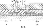
图10是在图1所示的半导体装置的制造方法的其它例子,规定的工序的剖面图。10 is a cross-sectional view of predetermined steps in another example of the method of manufacturing the semiconductor device shown in FIG. 1 .
图11是接着图12的工序的剖面图。Fig. 11 is a cross-sectional view of the step following Fig. 12 .
图12是作为本发明的第二实施例的半导体装置的剖面图。12 is a cross-sectional view of a semiconductor device as a second embodiment of the present invention.
图13是作为本发明的第三实施例的半导体装置的剖面图。13 is a cross-sectional view of a semiconductor device as a third embodiment of the present invention.
图14是在图13所示的半导体装置的制造方法的一个例子,规定的工序的剖面图。FIG. 14 is a cross-sectional view of predetermined steps in an example of the method of manufacturing the semiconductor device shown in FIG. 13 .
图15是接着图14工序的剖面图。Fig. 15 is a sectional view following the step of Fig. 14 .
图16是作为本发明的第四实施例的半导体装置的剖面图。16 is a cross-sectional view of a semiconductor device as a fourth embodiment of the present invention.
具体实施方式Detailed ways
(第一实施例)(first embodiment)
图1示出了作为本发明第一实施例的半导体装置的剖面图。该半导体装置称为CSP,具有硅基板(半导体基板)1。在硅基板1上面设置集成电路(图未示出),在上面周边部将铝类金属等构成的多个连接焊盘2与集成电路连接设置。FIG. 1 shows a cross-sectional view of a semiconductor device as a first embodiment of the present invention. This semiconductor device is called a CSP, and has a silicon substrate (semiconductor substrate) 1 . An integrated circuit (not shown) is provided on the upper surface of the
除了连接焊盘2的中央部的硅基板1的上面设置氧化硅等构成的绝缘膜3,连接焊盘2的中央部通过在绝缘膜3上设置的开口部4露出。在绝缘膜3的上面设置由聚酰亚胺类树脂等构成的保护膜5。在与绝缘膜3的开口部4相对应部分的保护膜5中设置开口部6。An
在保护膜5上面设置由铜等构成的底层金属层7。在底层金属层7的上面整体设置由铜构成的布线8。在含有底层金属层7的布线8的一端部通过绝缘膜3和保护膜5的开口部4、6与连接焊盘2相连接。在含有布线8的保护膜5的上面设置由聚酰亚胺类树脂等构成的保护膜9。在与布线8的连接焊盘部相对应部分中的保护膜9设置开口部10。An
通过保护膜9的开口部10露出的布线8的连接焊盘部上面、保护膜9的开口部10的内壁面及其周围中的保护膜9的上面设置由铜等组成的底层金属层11。在底层金属层11的上面整体设置由铜构成的突起电极12。An
此时,突起电极12由设置在保护膜9的开口部10内的下部突起电极部12a和在下部突起电极12a上面及其周围的保护膜9上设置的上部突起电极部12b组成。在突起电极12的上部突起电极部12b的上表面设置锡球13,该突起电极12的上部突起电极部12b的上面含有设置在保护膜9的上面的底层金属层11的端面。At this time, the
(制造方法的一例子)(an example of the production method)
接着,说明该半导体装置制造方法的一例。首先,如图2所示,在晶片状态的硅基板(以下称为半导体晶片21)的上面形成由铝类金属等组成的连接焊盘2、由氧化硅等组成的绝缘膜3和聚酰亚胺类树脂等组成的保护膜5,为了连接焊盘2的中央部通过形成在绝缘膜3和保护膜5中的开口部4、6露出。Next, an example of this semiconductor device manufacturing method will be described. First, as shown in FIG. 2, a
此时,半导体晶片21的上面形成各半导体装置的区域中形成规定的功能的集成电路(图未示出),连接焊盘2与分别对应部分中形成的集成电路电连接。另外,在图2中,用符号22所示的区域是与切割线相对应的区域。At this time, an integrated circuit (not shown) with a predetermined function is formed in the region where each semiconductor device is formed on the upper surface of the
接着,如图3所示,在含有通过绝缘膜3和保护膜5的开口部4、6露出的连接焊盘2的上面的保护膜5的上面整体形成底层金属层7。此时,底层金属层7可以仅是通过无电解电镀形成的铜层,另外可以仅是通过溅射形成的铜层,进一步可以是通过溅射形成的钛等的薄膜层上通过溅射形成铜层。Next, as shown in FIG. 3 , an
接着,在底层金属层7的上面图案化形成电镀抗蚀剂膜23。此时,在与布线8形成区域相对应的部分中的电镀抗蚀剂膜23中形成开口部24。接着,通过将底层金属层7作为电镀电流路进行铜电解电镀,在电镀抗蚀剂膜23的开口部24内的底层金属层7的上面形成布线8。接着,剥离电镀抗蚀剂膜23,接着,将布线8作为掩模(Mask)通过蚀刻(Etching)除去在布线8下以外的区域中的底层金属层7,则如图4所示,仅在布线8下残留底层金属层7。Next, a plating
接着,如图5所示,在含有布线8的保护膜5的上面,通过旋转涂敷(SpinCoat)法、转移模制(Transfer Mould)法等形成由聚酰亚胺类树脂等构成的保护膜9。接着,在与布线8连接焊盘部分相对应的部分中的保护膜9中通过光刻(Photolitho-graphy)法形成开口部10。Next, as shown in FIG. 5, on the upper surface of the
接着,如图6所示,在含有通过保护膜9的开口部10露出的布线8连接的焊盘部上面的保护膜9的上面的整体上,通过铜溅射等形成底层金属层11。接着,在底层金属层11的上面图案化形成电镀抗蚀剂膜25。Next, as shown in FIG. 6 , an
此时,在与突起电极12的上部突起电极部12b形成区域相对应的部分的电镀抗蚀剂膜25中形成比保护膜9的开口部10更大的开口部26。电镀抗蚀剂膜25的开口部26比保护膜9的开口部10更大是考虑到形成各开口部10、26时重合的精度。At this time, an
接着,通过将底层金属层11作为电镀电流路进行铜电解电镀,在保护膜9的开口部10内的底层金属层11内形成下部突起电极部12a,接着,在电镀抗蚀剂膜25的开口部26内的下部突起电极部12a和底层金属层11的上面形成上部突起电极部12b。Next, copper electrolytic plating is performed by using the
此时,由于电镀抗蚀剂膜25的开口部26比保护膜9的开口部10更大,所以在电镀保护膜25的开口部26内各向同性地堆积电镀。因此,在电镀抗蚀剂膜25的开口部26内形成的上部突起电极部12b成凸起的形状。接着,形成由下部突起电极部12a和上部突起电极部12b组成的突起电极12。At this time, since the
接着,剥离电镀抗蚀剂膜25,接着,将突起电极12作为掩模蚀刻除去突起电极12下以外的区域中的底层金属层11时,如图7所示,仅在突起电极12下残留底层金属层11。接着,在突起电极12的上部突起电极部12b上表面通过丝网(Screen)印刷法,涂敷焊剂(Flux)(未图示),接着,在焊剂上面搭载锡球(未图示)。Next, the plating resist
接着,经过回流工序,熔融在焊剂上面搭载的锡球后由于表面张力球形化固化,如图8所示,在含有保护膜9的上面形成的底层金属层11的端面的突起电极12的上部突起电极部12b的上表面形成锡球13。接着,如图9所示,将半导体晶片21、绝缘膜3、保护膜5和保护膜9沿着切割线22进行切割,得到图1所示的多个半导体装置。Next, after the reflow process, the solder balls mounted on the solder are melted and solidified due to surface tension, and as shown in FIG.
如上所述,在该半导体装置的制造方法的一例子中,在含有布线8的保护膜5上形成保护膜9,该保护膜9在与布线8连接焊盘部相对应部分具有开口部10,由于在保护膜9的开口部内10中布线8的连接焊盘部上通过电解电镀形成突起电极12,所以不需要称为研削这样的特殊工序。As described above, in an example of the manufacturing method of the semiconductor device, the
但是,在上述专利文献1记载的半导体装置的制造方法中,参考图3进行说明,剥离电镀抗蚀剂膜23,在含有布线8的底层金属层7的上表面形成突起电极形成用的电镀抗蚀剂膜,该突起电极形成用的电镀抗蚀剂膜在布线7的连接焊盘部相对应的部分具有开口部,通过将底层金属层7作为电镀电流路进行电解电镀,在突起电极形成用电镀抗蚀剂膜的开口部内的布线8的连接焊盘部上面形成突起电极,突起电极形成用电镀抗蚀剂膜通过使用抗蚀剂剥离液进行剥离,将布线8作为掩模蚀刻除去在布线8下以外区域中的底层金属层7。However, in the method of manufacturing a semiconductor device described in
但是,在上述专利文献1中记载的半导体装置的制造方法中,作为突起电极形成用电镀抗蚀剂膜使用干膜抗蚀剂时,将突起电极形成用电镀抗蚀剂膜使用抗蚀剂剥离液剥离时,由于突起电极形成用电镀抗蚀剂膜主要仅从其上侧面进行剥离,所以布线间的间隔变得狭窄,在布线间产生抗蚀剂残渣。该抗蚀剂残渣在将布线作为掩模进行蚀刻底层金属层时,构成掩模引起蚀刻不良,成为布线间的短路的原因。However, in the method of manufacturing a semiconductor device described in
对此,在上述半导体装置的制造方法的一例中,如图6所示,在含有布线8的保护膜5的上面形成保护膜9,由于在保护膜9的上面整体性形成底层金属层11的上面形成电镀抗蚀剂膜25,所以没有在布线8间插入电镀抗蚀剂膜25,进而可以在剥离电镀抗蚀剂膜25时不易产生抗蚀剂残渣。On the other hand, in one example of the manufacturing method of the above-mentioned semiconductor device, as shown in FIG. Since the plating resist
(制造方法的其它的例子)(other examples of the production method)
接着,说明如图1所示的半导体装置的制造方法的其他例子。首先,在如图6所示的工序中,如图10所示,在底层金属层11的上面图案化形成电镀抗蚀剂膜31。此时,电镀抗蚀剂膜31的厚度成为比图6所示的电镀抗蚀剂膜25厚度更大的厚度。另外,在突起电极12的上部突起电极部12b形成区域相对应部分的电镀抗蚀剂膜31中形成开口部32。Next, another example of the manufacturing method of the semiconductor device shown in FIG. 1 will be described. First, in the process shown in FIG. 6 , as shown in FIG. 10 , a plating resist
接着,通过将底层金属层11作为电镀电流路进行铜电解电镀,在保护膜9的开口部10内的底层金属层11内形成下部突起电极部12a,接着,在电镀抗蚀剂膜31的开口部32内的下部突起电极部12a和底层金属层11的上面形成上部突起电极部12b。进而,形成由下部突起电极部12a和上部突起电极部12b组成的突起电极12。Next, copper electrolytic plating is performed by using the
接着,通过将底层金属层11作为电镀电流路进行锡电解电镀,在电镀抗蚀剂膜31的开口部32内的突起电极12的上部突起电极部12b的上表面形成锡球形成用锡层13a。但是,此时在上述半导体装置的制造方法的一个例子中可以省略焊剂涂敷工序和锡球搭载工序。Next, by performing tin electrolytic plating using the
接着,剥离电镀抗蚀剂膜31,接着,锡球形成用锡层13a作为掩模的锡球形成用锡层13a下以外的区域中蚀刻除去底层金属层11,如图11所示,仅在锡球形成用锡层13a下的突起电极12下残留底层金属层11。Next, the electroplating resist
接着,通过回流工序,在熔融锡球形成用锡层13a后利用表面张力球形化固化,如图8所示,含有在保护膜9的上面形成的底层金属层11的端面的突起电极12的上部突起电极部12b上表面形成锡球13。以下的工序由于与上述半导体装置的制造方法的一例子情况相同,省略该说明。Next, through the reflow process, after the
在此,说明在图1中所示的半导体装置的一部分的尺寸的一例子。保护膜5的厚度是2~10μm。底层金属层7、11的铜层的厚度是0.3~1μm。布线8的厚度是1~20μm,优选3~8μm。保护膜9的厚度是20~120μm,优选30~80μm,但是也可以是100~120μm厚度。保护膜9的开口部的直径是80~300μm,但是随着布线8的微细化等,在突起电极12的下部突起电极部12a的直径变小时,也可以为20~200μm。突起电极12的上部突起电极部12b的高度以保护膜9上表面为基准,是10μm以下。Here, an example of the dimensions of a part of the semiconductor device shown in FIG. 1 will be described. The thickness of the
但是,在图1所示的半导体装置中,在突起电极12具有在下部突起电极部12a上具有上部突起电极部12b的结构,上部突起电极部12b的高度以保护膜9的上面为标准在10μm以下时进行说明,但是不对此限定。即突起电极12可以是上面为保护膜9的上面和一面即仅由下部突起电极部12a组成的结构。但是由于这样的面难以进行加工,如上所述,突起电极12可以在保护膜9的上面侧上可以例如10μm以下突起。However, in the semiconductor device shown in FIG. 1, the
(第二实施例)(second embodiment)
图12示出了作为本发明第二实施例的半导体装置的剖面图。在该半导体装置中,与图1所示的半导体装置不同的点,在突起电极12中,上部突起电极部12b的直径是相同的,但是下部突起电极部12a(保护膜9的开口部10)的直径更小的点。FIG. 12 shows a cross-sectional view of a semiconductor device as a second embodiment of the present invention. In this semiconductor device, the difference from the semiconductor device shown in FIG. 1 is that in the
在这样的情况下,与图1所示的半导体装置相比较,突起电极12间距是一定时,即使锡球13的支持部的上部突起电极部12b的直径相同,下部突起电极部12a(保护膜9的开口部10)的直径也会在某种程度地变小,由于下部突起电极部12a的支持部的布线8(含有底层金属层7)的连接焊盘部的直径可以变小,所以可以使布线8的连接焊盘部间的间隔变大,进而可以增加在布线8连接焊盘部间配置得到的布线8引回线部的数量,或者可以使设置在布线8引回线部的宽度等保持富余。In this case, compared with the semiconductor device shown in FIG. 1, when the pitch of the
(第三实施例)(third embodiment)
图13示出了作为该发明第三实施例的半导体装置的剖面图。在该半导体装置中,与图12所示的半导体装置不同的点,即使锡球13实质的直径相同,突起电极12的上部突起电极部12b的高度变高,上部突起电极部12b的表面上形成的锡球13和上部突起电极部12b的接合面积变大。在这样的情况下,由于锡球13和上部突起电极部12b的接合面积可以变大,所以可以将对锡球13的上部电极部12b的接合强度变大。FIG. 13 shows a cross-sectional view of a semiconductor device as a third embodiment of the invention. In this semiconductor device, the difference from the semiconductor device shown in FIG. 12 is that even if the
接着,说明该半导体装置的制造方法的一例子。此时,在如图10所示的工序中,如图14所示,在电镀抗蚀剂膜31的开口部32内使上部突起电极部12b的高度形成为20~200μm,优选形成为30~80μm,并在其上使锡球形成用锡层13a的高度为10~100μm,优选形成为20~50μm。Next, an example of a method of manufacturing the semiconductor device will be described. At this time, in the process shown in FIG. 10, as shown in FIG. 14, the height of the upper protruding
接着,剥离电镀抗蚀剂膜31,接着将锡球形成用锡层13a作为掩模蚀刻除去在锡球形成用锡层13a下以外区域中的底层金属层11,如图15所示,仅在锡球形成用锡层13a下的突起电极12下残存底层金属层11。接着,通过回流工序和切割工序,得到多个图13所示的半导体装置。Next, the electroplating resist
(第四实施例)(fourth embodiment)
图16示出了作为该发明第四实施例的半导体装置的剖面图。在该半导体装置中,与图13所示的半导体装置不同的点是省略锡球13,在突起电极12的上部突起电极部12b上表面形成表面处理层14。此时,例如在图14所示的工序中,连续进行底层金属层11作为电镀电流路的镍和金电解电镀,在电镀抗蚀剂膜31的开口部32内的上部突起电极部12b的上表面形成由镍和金组成的两层结构的表面处理层14。FIG. 16 shows a cross-sectional view of a semiconductor device as a fourth embodiment of the invention. This semiconductor device differs from the semiconductor device shown in FIG. 13 in that
Claims (5)
Applications Claiming Priority (2)
| Application Number | Priority Date | Filing Date | Title |
|---|---|---|---|
| JP302633/2006 | 2006-11-08 | ||
| JP2006302633 | 2006-11-08 |
Publications (2)
| Publication Number | Publication Date |
|---|---|
| CN101183668A CN101183668A (en) | 2008-05-21 |
| CN101183668Btrue CN101183668B (en) | 2012-01-11 |
Family
ID=39359037
Family Applications (1)
| Application Number | Title | Priority Date | Filing Date |
|---|---|---|---|
| CN2007101596981AActiveCN101183668B (en) | 2006-11-08 | 2007-11-08 | Semiconductor device having projecting electrode formed by electrolytic plating, and manufacturing method thereof |
Country Status (5)
| Country | Link |
|---|---|
| US (2) | US7619306B2 (en) |
| JP (1) | JP4922891B2 (en) |
| KR (1) | KR100956229B1 (en) |
| CN (1) | CN101183668B (en) |
| TW (1) | TW200832641A (en) |
Families Citing this family (16)
| Publication number | Priority date | Publication date | Assignee | Title |
|---|---|---|---|---|
| US8492263B2 (en) | 2007-11-16 | 2013-07-23 | Taiwan Semiconductor Manufacturing Company, Ltd. | Protected solder ball joints in wafer level chip-scale packaging |
| JP2010062170A (en)* | 2008-09-01 | 2010-03-18 | Casio Comput Co Ltd | Semiconductor device and manufacturing method thereof |
| JP2010062176A (en)* | 2008-09-01 | 2010-03-18 | Casio Comput Co Ltd | Semiconductor device and manufacturing method thereof |
| JP2010087229A (en)* | 2008-09-30 | 2010-04-15 | Sanyo Electric Co Ltd | Semiconductor module, method of manufacturing semiconductor module, and portable device |
| US8318596B2 (en) | 2010-02-11 | 2012-11-27 | Taiwan Semiconductor Manufacturing Company, Ltd. | Pillar structure having a non-planar surface for semiconductor devices |
| US8803319B2 (en) | 2010-02-11 | 2014-08-12 | Taiwan Semiconductor Manufacturing Company, Ltd. | Pillar structure having a non-planar surface for semiconductor devices |
| KR101701380B1 (en)* | 2010-08-17 | 2017-02-01 | 해성디에스 주식회사 | Device embedded flexible printed circuit board and manufacturing method thereof |
| JP5587702B2 (en)* | 2010-08-26 | 2014-09-10 | 株式会社テラプローブ | Semiconductor device and manufacturing method of semiconductor device |
| JP2012074581A (en)* | 2010-09-29 | 2012-04-12 | Teramikros Inc | Semiconductor device and method for manufacturing the same |
| JP5535114B2 (en)* | 2011-03-25 | 2014-07-02 | 株式会社東芝 | Light emitting device, light emitting module, and method of manufacturing light emitting device |
| JP5782823B2 (en)* | 2011-04-27 | 2015-09-24 | 日亜化学工業株式会社 | Nitride semiconductor light emitting device and manufacturing method thereof |
| KR20140108546A (en) | 2011-12-08 | 2014-09-11 | 코닌클리케 필립스 엔.브이. | Semiconductor light emitting device with thick metal layers |
| US9230932B2 (en) | 2012-02-09 | 2016-01-05 | Taiwan Semiconductor Manufacturing Company, Ltd. | Interconnect crack arrestor structure and methods |
| US9515036B2 (en) | 2012-04-20 | 2016-12-06 | Taiwan Semiconductor Manufacturing Company, Ltd. | Methods and apparatus for solder connections |
| DE102015214228A1 (en) | 2015-07-28 | 2017-02-02 | Osram Opto Semiconductors Gmbh | Method for producing a component and a component |
| US11296030B2 (en)* | 2019-04-29 | 2022-04-05 | Advanced Semiconductor Engineering, Inc. | Embedded component package structure and manufacturing method thereof |
Family Cites Families (19)
| Publication number | Priority date | Publication date | Assignee | Title |
|---|---|---|---|---|
| JP2001144228A (en) | 1999-11-12 | 2001-05-25 | Sanyo Electric Co Ltd | Semiconductor device and ite manufacturing method |
| JP2002064163A (en)* | 2000-08-21 | 2002-02-28 | Ibiden Co Ltd | Semiconductor chip |
| JP3886712B2 (en) | 2000-09-08 | 2007-02-28 | シャープ株式会社 | Manufacturing method of semiconductor device |
| US6870276B1 (en)* | 2001-12-26 | 2005-03-22 | Micron Technology, Inc. | Apparatus for supporting microelectronic substrates |
| TW577160B (en) | 2002-02-04 | 2004-02-21 | Casio Computer Co Ltd | Semiconductor device and manufacturing method thereof |
| US6770971B2 (en)* | 2002-06-14 | 2004-08-03 | Casio Computer Co., Ltd. | Semiconductor device and method of fabricating the same |
| WO2004015771A2 (en) | 2002-08-09 | 2004-02-19 | Casio Computer Co., Ltd. | Semiconductor device and method of manufacturing the same |
| TWI244129B (en)* | 2002-10-25 | 2005-11-21 | Via Tech Inc | Bonding column process |
| JP2004335915A (en) | 2003-05-12 | 2004-11-25 | Shinko Electric Ind Co Ltd | Method for manufacturing semiconductor device |
| JP4130158B2 (en)* | 2003-06-09 | 2008-08-06 | 三洋電機株式会社 | Semiconductor device manufacturing method, semiconductor device |
| JP2005175128A (en)* | 2003-12-10 | 2005-06-30 | Fujitsu Ltd | Semiconductor device and manufacturing method thereof |
| JP4381191B2 (en)* | 2004-03-19 | 2009-12-09 | Okiセミコンダクタ株式会社 | Semiconductor package and semiconductor device manufacturing method |
| JP4119866B2 (en)* | 2004-05-12 | 2008-07-16 | 富士通株式会社 | Semiconductor device |
| JP4042749B2 (en) | 2005-02-21 | 2008-02-06 | カシオ計算機株式会社 | Manufacturing method of semiconductor device |
| JP4395775B2 (en)* | 2005-10-05 | 2010-01-13 | ソニー株式会社 | Semiconductor device and manufacturing method thereof |
| JP4755486B2 (en)* | 2005-11-17 | 2011-08-24 | Okiセミコンダクタ株式会社 | Semiconductor device and manufacturing method thereof |
| JP4609317B2 (en)* | 2005-12-28 | 2011-01-12 | カシオ計算機株式会社 | Circuit board |
| US8749065B2 (en)* | 2007-01-25 | 2014-06-10 | Tera Probe, Inc. | Semiconductor device comprising electromigration prevention film and manufacturing method thereof |
| JP4538764B2 (en)* | 2008-07-24 | 2010-09-08 | カシオ計算機株式会社 | Semiconductor device and manufacturing method thereof |
- 2007
- 2007-10-05JPJP2007261479Apatent/JP4922891B2/enactiveActive
- 2007-11-07USUS11/936,179patent/US7619306B2/enactiveActive
- 2007-11-07TWTW096141985Apatent/TW200832641A/enunknown
- 2007-11-07KRKR1020070113162Apatent/KR100956229B1/enactiveActive
- 2007-11-08CNCN2007101596981Apatent/CN101183668B/enactiveActive
- 2009
- 2009-09-24USUS12/566,423patent/US8097941B2/enactiveActive
Also Published As
| Publication number | Publication date |
|---|---|
| KR100956229B1 (en) | 2010-05-04 |
| JP2008141170A (en) | 2008-06-19 |
| JP4922891B2 (en) | 2012-04-25 |
| TW200832641A (en) | 2008-08-01 |
| CN101183668A (en) | 2008-05-21 |
| US20100015795A1 (en) | 2010-01-21 |
| US7619306B2 (en) | 2009-11-17 |
| KR20080042010A (en) | 2008-05-14 |
| US8097941B2 (en) | 2012-01-17 |
| US20080105981A1 (en) | 2008-05-08 |
Similar Documents
| Publication | Publication Date | Title |
|---|---|---|
| CN101183668B (en) | Semiconductor device having projecting electrode formed by electrolytic plating, and manufacturing method thereof | |
| KR100455404B1 (en) | A semiconductor device and method for manufacturing the same | |
| US20040007779A1 (en) | Wafer-level method for fine-pitch, high aspect ratio chip interconnect | |
| US20070145603A1 (en) | Semiconductor chip, mounting structure thereof, and methods for forming a semiconductor chip and printed circuit board for the mounting structure thereof | |
| CN102254876A (en) | Semiconductor apparatus and semiconductor apparatus unit | |
| JP2012054359A (en) | Semiconductor device and manufacturing method of semiconductor device | |
| TWI413210B (en) | An electronic device package and method of manufacture | |
| JP2010087229A (en) | Semiconductor module, method of manufacturing semiconductor module, and portable device | |
| JP5385452B2 (en) | Manufacturing method of semiconductor device | |
| JP2010114140A (en) | Semiconductor device and method of manufacturing the same | |
| TWI419284B (en) | Chip bump structure and method for forming chip bump structure | |
| JP4506767B2 (en) | Manufacturing method of semiconductor device | |
| JP2011249564A (en) | Semiconductor device manufacturing method and mounting structure | |
| TW200826267A (en) | Wafer level chip package and a method of fabricating thereof | |
| JP4506168B2 (en) | Semiconductor device and its mounting structure | |
| JP3972211B2 (en) | Semiconductor device and manufacturing method thereof | |
| JP2008028109A (en) | Semiconductor device and manufacturing method therefor | |
| US7541273B2 (en) | Method for forming bumps | |
| JP4686962B2 (en) | Manufacturing method of semiconductor device | |
| JP2001077142A (en) | Semiconductor device and manufacturing method thereof | |
| WO2020213133A1 (en) | Semiconductor device | |
| JP2004172163A (en) | Semiconductor device and manufacturing method thereof | |
| JP5068830B2 (en) | Semiconductor device | |
| TW202504030A (en) | Semiconductor chip and method for manufacturing semiconductor chip | |
| US8314345B2 (en) | Device mounting board and semiconductor module |
Legal Events
| Date | Code | Title | Description |
|---|---|---|---|
| C06 | Publication | ||
| PB01 | Publication | ||
| C10 | Entry into substantive examination | ||
| SE01 | Entry into force of request for substantive examination | ||
| C14 | Grant of patent or utility model | ||
| GR01 | Patent grant | ||
| ASS | Succession or assignment of patent right | Owner name:ZHAOZHUANGWEI CO., LTD. Free format text:FORMER OWNER: CASIO COMPUTER CO., LTD. Effective date:20120309 | |
| C41 | Transfer of patent application or patent right or utility model | ||
| TR01 | Transfer of patent right | Effective date of registration:20120309 Address after:Tokyo, Japan Patentee after:Zhaozhuang Micro Co.,Ltd. Address before:Tokyo, Japan Patentee before:CASIO COMPUTER Co.,Ltd. | |
| TR01 | Transfer of patent right | Effective date of registration:20170320 Address after:Kagawa Patentee after:AOI ELECTRONICS Co.,Ltd. Address before:Kanagawa Patentee before:Zhao Tan Jing Co.,Ltd. Effective date of registration:20170320 Address after:Kanagawa Patentee after:Zhao Tan Jing Co.,Ltd. Address before:Tokyo, Japan Patentee before:Zhaozhuang Micro Co.,Ltd. | |
| TR01 | Transfer of patent right |