CN101178524B - LCDs with integrated touch panels - Google Patents
LCDs with integrated touch panelsDownload PDFInfo
- Publication number
- CN101178524B CN101178524BCN2007101651936ACN200710165193ACN101178524BCN 101178524 BCN101178524 BCN 101178524BCN 2007101651936 ACN2007101651936 ACN 2007101651936ACN 200710165193 ACN200710165193 ACN 200710165193ACN 101178524 BCN101178524 BCN 101178524B
- Authority
- CN
- China
- Prior art keywords
- line
- pseudo
- sensor
- lines
- gate
- Prior art date
- Legal status (The legal status is an assumption and is not a legal conclusion. Google has not performed a legal analysis and makes no representation as to the accuracy of the status listed.)
- Expired - Fee Related
Links
Images


Classifications
- G—PHYSICS
- G02—OPTICS
- G02F—OPTICAL DEVICES OR ARRANGEMENTS FOR THE CONTROL OF LIGHT BY MODIFICATION OF THE OPTICAL PROPERTIES OF THE MEDIA OF THE ELEMENTS INVOLVED THEREIN; NON-LINEAR OPTICS; FREQUENCY-CHANGING OF LIGHT; OPTICAL LOGIC ELEMENTS; OPTICAL ANALOGUE/DIGITAL CONVERTERS
- G02F1/00—Devices or arrangements for the control of the intensity, colour, phase, polarisation or direction of light arriving from an independent light source, e.g. switching, gating or modulating; Non-linear optics
- G02F1/01—Devices or arrangements for the control of the intensity, colour, phase, polarisation or direction of light arriving from an independent light source, e.g. switching, gating or modulating; Non-linear optics for the control of the intensity, phase, polarisation or colour
- G02F1/13—Devices or arrangements for the control of the intensity, colour, phase, polarisation or direction of light arriving from an independent light source, e.g. switching, gating or modulating; Non-linear optics for the control of the intensity, phase, polarisation or colour based on liquid crystals, e.g. single liquid crystal display cells
- G02F1/133—Constructional arrangements; Operation of liquid crystal cells; Circuit arrangements
- G02F1/1333—Constructional arrangements; Manufacturing methods
- G02F1/13338—Input devices, e.g. touch panels
- G—PHYSICS
- G06—COMPUTING OR CALCULATING; COUNTING
- G06F—ELECTRIC DIGITAL DATA PROCESSING
- G06F3/00—Input arrangements for transferring data to be processed into a form capable of being handled by the computer; Output arrangements for transferring data from processing unit to output unit, e.g. interface arrangements
- G06F3/01—Input arrangements or combined input and output arrangements for interaction between user and computer
- G06F3/03—Arrangements for converting the position or the displacement of a member into a coded form
- G06F3/041—Digitisers, e.g. for touch screens or touch pads, characterised by the transducing means
- G06F3/0412—Digitisers structurally integrated in a display
- G—PHYSICS
- G06—COMPUTING OR CALCULATING; COUNTING
- G06F—ELECTRIC DIGITAL DATA PROCESSING
- G06F3/00—Input arrangements for transferring data to be processed into a form capable of being handled by the computer; Output arrangements for transferring data from processing unit to output unit, e.g. interface arrangements
- G06F3/01—Input arrangements or combined input and output arrangements for interaction between user and computer
- G06F3/03—Arrangements for converting the position or the displacement of a member into a coded form
- G06F3/041—Digitisers, e.g. for touch screens or touch pads, characterised by the transducing means
- G06F3/0416—Control or interface arrangements specially adapted for digitisers
- G06F3/0418—Control or interface arrangements specially adapted for digitisers for error correction or compensation, e.g. based on parallax, calibration or alignment
- G—PHYSICS
- G06—COMPUTING OR CALCULATING; COUNTING
- G06F—ELECTRIC DIGITAL DATA PROCESSING
- G06F3/00—Input arrangements for transferring data to be processed into a form capable of being handled by the computer; Output arrangements for transferring data from processing unit to output unit, e.g. interface arrangements
- G06F3/01—Input arrangements or combined input and output arrangements for interaction between user and computer
- G06F3/03—Arrangements for converting the position or the displacement of a member into a coded form
- G06F3/041—Digitisers, e.g. for touch screens or touch pads, characterised by the transducing means
- G06F3/047—Digitisers, e.g. for touch screens or touch pads, characterised by the transducing means using sets of wires, e.g. crossed wires
Landscapes
- Engineering & Computer Science (AREA)
- Physics & Mathematics (AREA)
- General Engineering & Computer Science (AREA)
- Theoretical Computer Science (AREA)
- General Physics & Mathematics (AREA)
- Human Computer Interaction (AREA)
- Nonlinear Science (AREA)
- Chemical & Material Sciences (AREA)
- Crystallography & Structural Chemistry (AREA)
- Mathematical Physics (AREA)
- Optics & Photonics (AREA)
- Liquid Crystal (AREA)
- Position Input By Displaying (AREA)
- Devices For Indicating Variable Information By Combining Individual Elements (AREA)
Abstract
Translated fromChinese
Description
Translated fromChinese技术领域technical field
本发明涉及具有集成触摸面板的液晶显示器(LCD),更具体地,涉及通过消除耦合噪声来防止传感器故障的具有集成触摸面板的LCD。The present invention relates to a liquid crystal display (LCD) with an integrated touch panel, and more particularly, to an LCD with an integrated touch panel that prevents sensor failure by eliminating coupling noise.
背景技术Background technique
众所周知能够显示图像的各种显示装置,包括阴极射线管(CRT)、液晶显示器(LCD)、等离子体显示器(PDP)等。在这些显示装置中,触摸面板可被用作适合感测显示屏上被施加压力的位置的输入装置,从而,触摸面板的用户可以容易地通过钢笔、手指等触摸显示屏来输入数据。Various display devices capable of displaying images are well known, including cathode ray tubes (CRTs), liquid crystal displays (LCDs), plasma displays (PDPs), and the like. Among these display devices, a touch panel can be used as an input device suitable for sensing a position on a display screen to which pressure is applied, so that a user of the touch panel can easily input data by touching the display screen with a pen, finger, or the like.
为了解决涉及触摸面板的厚度或尺寸的问题,目前正在开发具有集成触摸面板的新型LCD。在这些新型LCD中,进行努力以降低触摸面板的厚度,这是制造薄LCD的有利特征。此外,因为不必要组装单独的模块,所以这些新的LCD对于增加产量尤其有效。To address issues involving the thickness or size of the touch panel, new LCDs with integrated touch panels are currently being developed. In these new LCDs, efforts are being made to reduce the thickness of the touch panel, which is an advantageous feature for making thin LCDs. In addition, these new LCDs are especially effective for increasing yields because it is not necessary to assemble individual modules.
在具有集成触摸面板的LCD中,响应于手指等的外压,形成在共用电极面板上的共用电极与形成在薄膜晶体管(TFT)阵列面板上的传感器电极接触,使得将预定电压施加到传感器线,然后将其提供给传感器以输出具有特定电平的信号。In an LCD with an integrated touch panel, in response to external pressure from a finger or the like, a common electrode formed on the common electrode panel comes into contact with a sensor electrode formed on a thin film transistor (TFT) array panel, so that a predetermined voltage is applied to the sensor lines , which is then provided to the sensor to output a signal with a specific level.
然而,在这种配置中,由于形成在TFT阵列面板上的数据线和形成在共用电极面板上的共用电极之间的耦合,会发生共用电压失真。只要将数据电压施加给数据线,共用电压就变得严重失真。因此,通过传感器线将失真的共用电压提供给传感器,并且由于传感器确定两个信号(即,具有特定电平的参考信号和由失真的共用电压获得的信号)的极性,所以极性可能被错误确定。从而,即使当没有将外压施加到触摸面板时,也可能错误地报告施加了外压。此外,当将外压施加到触摸面板时,难以确定表示对应于该外压的实际位置的坐标信号。However, in this configuration, common voltage distortion occurs due to coupling between data lines formed on the TFT array panel and common electrodes formed on the common electrode panel. As long as the data voltage is applied to the data lines, the common voltage becomes severely distorted. Therefore, a distorted common voltage is supplied to the sensor through the sensor line, and since the sensor determines the polarity of two signals (i.e., a reference signal with a certain level and a signal obtained from the distorted common voltage), the polarity may be distorted. Error OK. Thus, even when no external pressure is applied to the touch panel, it may be erroneously reported that external pressure is applied. Furthermore, when external pressure is applied to the touch panel, it is difficult to determine a coordinate signal representing an actual position corresponding to the external pressure.
发明内容Contents of the invention
根据本文描述的示例性实施例,提供了通过消除耦合噪声来防止传感器故障的具有集成触摸面板的LCD。According to the exemplary embodiments described herein, there is provided an LCD with an integrated touch panel that prevents sensor failure by eliminating coupling noise.
在一个示例性实施例中,LCD包括:绝缘衬底;多条栅极线,形成在绝缘衬底上以在第一方向上延伸;多条数据线,形成在第二方向上以与栅极线交叉;多个薄膜晶体管(TFT),每一个都形成在由栅极线和数据线定义的区域处;多条传感器线,形成在与栅极线和数据线相同的方向上;以及多条伪线(dummy line),形成在与传感器线相同的方向上。In one exemplary embodiment, an LCD includes: an insulating substrate; a plurality of gate lines formed on the insulating substrate to extend in a first direction; a plurality of data lines formed in a second direction to connect with the gate lines. Lines cross; a plurality of thin film transistors (TFTs), each formed at a region defined by the gate line and the data line; a plurality of sensor lines, formed in the same direction as the gate line and the data line; and a plurality of A dummy line, formed in the same direction as the sensor line.
在另一个示例性实施例中,具有集成触摸面板的LCD包括:薄膜晶体管(TFT)阵列面板,其包括形成在绝缘层衬底上以在第一方向上延伸的多条栅极线、形成在第二方向上以与栅极线交叉的多条数据线、每一个都形成在由栅极线和数据线定义的区域处的多个薄膜晶体管(TFT)、形成在与栅极线和数据线相同的方向上的多条传感器线、形成在与传感器线相同的方向上的多条伪线;以及印刷电路板,其包括用于将预定电压施加给伪线的第一互连线、用于在连接至多条栅极线的栅极驱动器中施加栅极截止电压的第二互连线、以及耦合在第一互连线和第二互连线之间用于消除耦合噪声的电容器。In another exemplary embodiment, an LCD with an integrated touch panel includes: a thin film transistor (TFT) array panel including a plurality of gate lines formed on an insulating layer substrate to extend in a first direction, formed on A plurality of data lines intersecting the gate lines in the second direction, a plurality of thin film transistors (TFTs) each formed at a region defined by the gate lines and the data lines, formed between the gate lines and the data lines a plurality of sensor lines in the same direction, a plurality of dummy wires formed in the same direction as the sensor lines; and a printed circuit board including a first interconnection for applying a predetermined voltage to the dummy wires, for A second interconnection line applying a gate-off voltage in a gate driver connected to the plurality of gate lines, and a capacitor coupled between the first interconnection line and the second interconnection line for eliminating coupling noise.
从下面一些示例性实施例的详细描述中可以获得对本发明新的触摸屏LCD的上述内容更好的理解和很多其它特征和优点,尤其是这种描述与附图相结合,在附图中,相同的参考标号用于确定在一副或多幅图中示出的相同元件。A better understanding of the above and many other features and advantages of the new touch screen LCD of the present invention can be obtained from the following detailed description of some exemplary embodiments, especially if this description is taken in conjunction with the accompanying drawings, in which the same Reference numerals are used to identify identical elements shown in one or more figures.
附图说明Description of drawings
图1是根据本发明的具有集成触摸面板的LCD的第一示例性实施例的部分示意图;1 is a partial schematic diagram of a first exemplary embodiment of an LCD with an integrated touch panel according to the present invention;
图2是由图1中的虚线‘A’包围的图1的示例性LCD的部分放大示意详图;Figure 2 is a partially enlarged schematic detail view of the exemplary LCD of Figure 1 surrounded by dashed line 'A' in Figure 1;
图3A是示出单个示例性像素的图1示例性LCD的薄膜晶体管(TFT)阵列面板的部分平面图;3A is a partial plan view of a thin film transistor (TFT) array panel of the exemplary LCD of FIG. 1 showing a single exemplary pixel;
图3B是沿图3A中截面IIIb-IIIb’的线看到的TFT阵列面板的部分截面图;Fig. 3 B is a partial sectional view of the TFT array panel seen along the line of section IIIb-IIIb' in Fig. 3A;
图3C是沿图3A中截面IIIc-IIIC’和IIIc’-IIIC”的线看到的TFT阵列面板的放大部分截面图;Figure 3C is an enlarged partial cross-sectional view of the TFT array panel seen along the lines of section IIIc-IIIC' and IIIc'-IIIC in Figure 3A;
图4是示出单个示例性像素的图1示例性LCD的共用电极面板的部分平面图;4 is a partial plan view of a common electrode panel of the exemplary LCD of FIG. 1 showing a single exemplary pixel;
图5A是示出单个示例性像素的包括图3A的TFT阵列面板和图4的共用电极面板的具有集成触摸面板的示例性LCD的部分平面图;5A is a partial plan view of an exemplary LCD with an integrated touch panel including the TFT array panel of FIG. 3A and the common electrode panel of FIG. 4 showing a single exemplary pixel;
图5B是沿图3A中截面Vb-Vb’的线看到的TFT阵列面板的部分截面图;Figure 5B is a partial sectional view of the TFT array panel seen along the line of section Vb-Vb' in Figure 3A;
图6是根据本发明的具有集成触摸面板的LCD的第二示例性实施例的部分示意图;6 is a partial schematic diagram of a second exemplary embodiment of an LCD with an integrated touch panel according to the present invention;
图7是根据本发明的具有集成触摸面板的LCD的第三示例性实施例的部分示意图;7 is a partial schematic diagram of a third exemplary embodiment of an LCD with an integrated touch panel according to the present invention;
图8是根据本发明的具有集成触摸面板的LCD的第四示例性实施例的部分示意图;以及8 is a partial schematic diagram of a fourth exemplary embodiment of an LCD with an integrated touch panel according to the present invention; and
图9是根据本发明的具有集成触摸面板的LCD第五示例性实施例的部分示意图。9 is a partial schematic diagram of a fifth exemplary embodiment of an LCD with an integrated touch panel according to the present invention.
具体实施方式Detailed ways
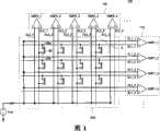
图1是根据本发明的具有集成触摸面板的LCD的第一示例性实施例的部分示意图,图2是由图1中的虚线‘A’包围的示例性LCD部分的放大示意详图,图3A是示出单个示例性像素的图1示例性LCD的薄膜晶体管(TFT)阵列面板的部分平面图,图3B是沿图3A中截面IIIb-IIIb’的线看到的TFT阵列面板的部分截面图,以及图3C是沿图3A中的截面IIIc-IIIC’和IIIc’-IIIC”的线看到的TFT阵列面板的放大部分截面图。1 is a partial schematic diagram of a first exemplary embodiment of an LCD with an integrated touch panel according to the present invention, FIG. 2 is an enlarged schematic detail view of a portion of the exemplary LCD surrounded by dashed line 'A' in FIG. 1 , and FIG. 3A is a partial plan view of the thin film transistor (TFT) array panel of the exemplary LCD of FIG. 1 showing a single exemplary pixel, and FIG. 3B is a partial cross-sectional view of the TFT array panel seen along the line of section IIIb-IIIb' in FIG. 3A , And FIG. 3C is an enlarged partial cross-sectional view of the TFT array panel seen along the lines of sections IIIc-IIIC' and IIIc'-IIIC" in FIG. 3A.
参考图1,在具有集成触摸面板的第一示例性LCD中,其TFT阵列面板100包括触摸面板,其在将外压施加到面板时,输出对应于触摸面板上的触摸位置的坐标信号。Referring to FIG. 1 , in a first exemplary LCD with an integrated touch panel, its
在TFT阵列面板100的绝缘衬底上通常垂直的第一和第二方向上分别形成相应的多条第一和第二传感器线SL1_1至SL1_4和SL2_1至SL2_5,以及在与第一和第二传感器线SL1_1至SL1_4和SL2_1至SL2_5相同的方向上在其上还分别形成相应的多条第一和第二伪线AL1_1至AL1_4和AL2_1至AL2_5。将参考电压Vref施加给第一和第二伪线AL1_1至AL1_4和AL2_1至AL2_5。A corresponding plurality of first and second sensor lines SL1_1 to SL1_4 and SL2_1 to SL2_5 are respectively formed on the insulating substrate of the
第一和第二传感器线SL1_1至SL1_4和SL2_1至SL2_5分别连接至第一和第二传感器电极28a和63a。当将外压施加到传感器电极的关联对附近的显示器的正面时,将形成在共用电极面板200上的传感器隔离物(spacer)92电连接至TFT阵列面板100的第一和第二传感器电极28a和63a,使得将预定电压传输到第一和第二传感器线SL1_1至SL1_4和SL2_1至SL2_5。The first and second sensor lines SL1_1 to SL1_4 and SL2_1 to SL2_5 are connected to the first and
此外,TFT阵列面板100包括多个第一比较器AMP1_1至AMP1_4以及多个第二比较器AMP2_1至AMP2_5,其中,第一比较器AMP1_1至AMP1_4分别连接至第一传感器线SL1_1至SL1_4和第一伪线AL1_1至AL1_4,并放大每条第一传感器线SL1_1至SL1_4和每条第一伪线AL1_1至AL1_4之间的电压差,然后输出放大的电压差,以及第二比较器AMP2_1至AMP2_5分别连接至第二传感器线SL2_1至SL2_5和第二伪线AL2_1至AL2_5,并放大每条第二传感器线SL2_1至SL2_5和每条第二伪线AL2_1至AL2_5之间的电压差,然后输出放大的电压差。In addition, the
下面描述在第一示例性实施例中在与第一和第二传感器SL1_1至SL1_4和SL2_1至SL2_5相同的方向上分别形成第一和第二伪线AL1_1至AL1_4和AL2_1至AL2_5的目的。The following describes the purpose of forming the first and second dummy wires AL1_1 to AL1_4 and AL2_1 to AL2_5 in the same direction as the first and second sensors SL1_1 to SL1_4 and SL2_1 to SL2_5 , respectively, in the first exemplary embodiment.
在传统的触摸屏实施例中,由于形成在TFT阵列面板100上的数据线(未示出)和形成在共用电极面板200上的共用电极(未示出)之间的耦合,共用电压可能会失真。只要施加给数据线的数据电压存在变化,这种共用电压失真就变得更加严重。结果,失真的共用电压被传输到第一和第二传感器线SL1_1至SL1_4和SL2_1至SL2_5,然后,第一和第二比较器AMP1_1至AMP1_4和AMP2_1至AMP2_5可能错误地确定两个信号(即,具有特定电平的参考信号和由失真的共用电压获得的信号)的极性。因此,即使没有外压施加到显示器,触摸传感器机构可能仍然指示正在施加外压。此外,即使实际上施加外压,也非常难以确定对应于外压的触摸位置的实际坐标。In conventional touch screen embodiments, the common voltage may be distorted due to coupling between data lines (not shown) formed on the
为了解决这个问题,在与第一和第二传感器线SL1_1至SL1_4和SL2_1至SL2_5相同的方向上分别形成第一和第二伪线AL1_1至AL1_4和AL2_1至AL2_5,从而确保当第一和第二传感器线SL1_1至SL1_4和SL2_1至SL2_5被来自共用电极面板200的共用电极的耦合所影响时,第一和第二伪线AL1_1至AL1_4和AL2_1至AL2_5类似地被与第一和第二传感器线SL1_1至SL1_4和SL2_1至SL2_5的耦合所影响。To solve this problem, the first and second dummy lines AL1_1 to AL1_4 and AL2_1 to AL2_5 are formed in the same direction as the first and second sensor lines SL1_1 to SL1_4 and SL2_1 to SL2_5, respectively, thereby ensuring that when the first and second When the sensor lines SL1_1 to SL1_4 and SL2_1 to SL2_5 are affected by coupling from the common electrode of the
第一和第二伪线AL1_1至AL1_4和AL2_1至AL2_5与第一和第二传感器线SL1_1至SL1_4和SL2_1至SL2_5具有基本相同的相位。因此,通过第一和第二传感器线SL1_1至SL1_4和SL2_1至SL2_5将共用电压施加给第一和第二比较器AMP1_1至AMP1_4和AMP2_1至AMP2_5,以及将与共用电压具有相同相位的参考电压施加给第一和第二伪线AL1_1至AL1_4和AL2_1至AL2_5。接下来,第一和第二比较器AMP1_1至AMP1_4和AMP2_1至AMP2_5将共用电压和参考电压进行比较,并基于比较结果将表示对应于触摸位置的坐标数据的预定感测电压输出至第一和第二比较器AMP1_1至AMP1_4和AMP2_1至AMP2_5的输出端。因此,由于第一和第二比较器AMP1_1至AMP1_4和AMP2_1至AMP2_5将共用电压和与共用电压具有相同相位的参考电压进行比较,所以防止了由确定相对极性而引起的极性错误确定。The first and second dummy lines AL1_1 to AL1_4 and AL2_1 to AL2_5 have substantially the same phase as the first and second sensor lines SL1_1 to SL1_4 and SL2_1 to SL2_5 . Therefore, a common voltage is applied to the first and second comparators AMP1_1 to AMP1_4 and AMP2_1 to AMP2_5 through the first and second sensor lines SL1_1 to SL1_4 and SL2_1 to SL2_5, and a reference voltage having the same phase as the common voltage is applied to The first and second dummy wires AL1_1 to AL1_4 and AL2_1 to AL2_5. Next, the first and second comparators AMP1_1 to AMP1_4 and AMP2_1 to AMP2_5 compare the common voltage with the reference voltage, and output a predetermined sensing voltage representing coordinate data corresponding to the touched position to the first and second comparators based on the comparison result. Output terminals of two comparators AMP1_1 to AMP1_4 and AMP2_1 to AMP2_5. Therefore, since the first and second comparators AMP1_1 to AMP1_4 and AMP2_1 to AMP2_5 compare the common voltage with the reference voltage having the same phase as the common voltage, polarity erroneous determination caused by determining the relative polarity is prevented.
图2是示出显示包括触摸面板的信号线和像素的等效电路图,其中,显示信号线包括由GL表示的栅极线和由DL表示的数据线。2 is an equivalent circuit diagram showing a display including signal lines and pixels of a touch panel, wherein the display signal lines include gate lines denoted by GL and data lines denoted by DL.
参考图2,每个像素PX都包括连接至相应的一条栅极线GL和相应的一条数据线DL的开关装置Q、连接至开关装置Q的液晶电容器、以及存储电容器。Referring to FIG. 2 , each pixel PX includes a switching device Q connected to a corresponding one of the gate lines GL and a corresponding one of the data lines DL, a liquid crystal capacitor connected to the switching device Q, and a storage capacitor.
此外,像素PX包括形成在与栅极线GL相同方向上的第一传感器线SL1_1和第一伪线AL1_1、形成在与数据线DL相同方向上的第二传感器线SL2_4和第二伪线AL2_4、连接至第一和第二传感器线SL1_1和SL2_4中相应一条的第一传感器电极28a和第二传感器电极63a、连接至第一传感器线SL1_1和第一伪线AL1_1的第一比较器AMP1_1、以及连接至第二传感器线SL2_4和第二伪线AL2_4的第二比较器AMP2_4。In addition, the pixel PX includes a first sensor line SL1_1 and a first dummy line AL1_1 formed in the same direction as the gate line GL, a second sensor line SL2_4 and a second dummy line AL2_4 formed in the same direction as the data line DL, The
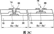
参考图3A至图3C,在图中的水平方向上,在绝缘衬底10上形成栅极线22,并且以突出的形式在栅极线22上形成栅电极26。在栅极线22的末端形成栅极线端部24以从其它层或从外部接收选通信号并将接收到的选通信号传输到栅极线22。扩展栅极线端部24的宽度用于连接至外部电路。栅极线22、栅电极26、以及栅极线端部24构成栅极互连线(22、26、24)。Referring to FIGS. 3A to 3C , in the horizontal direction in the drawings,
此外,存储电极25与像素电极82(下面进行详细描述)重叠以形成存储电容器,这提高了像素的充电保持能力。存储电极25的形状和配置可与所示出的大大不同。In addition, the
在与栅极线22相同的方向上,在绝缘衬底10上形成第一传感器线28b,以及在与第一传感器线28b相同的方向上,在绝缘衬底10上形成具有扩展宽度的第一传感器电极28a。第一传感器电极28a包括触摸面板传感器的一端并通过接触孔72连接至第一传感器焊盘(pad)84。当将外压施加给传感器焊盘附近的面板时,将第一传感器电极28a电连接至下面详细描述的传感器隔离物92上的共用电极(参见图4),然后提供对应于施加有外压(例如,手指触摸)的位置的位置信息。第一传感器电极28a和第一传感器线28b构成第一传感器互连线。此外,在与第一传感器互连线28a和28b相同的方向上形成第一伪线29。在示出的实施例中,在与栅极互连线(22、24、26)相同的层中形成第一传感器互连线28a和28b以及第一伪线29。In the same direction as the
优选地,栅极互连线(22、24、26)、存储电极25、第一传感器互连线28a和28b、以及第一伪线29由含铝金属(例如,铝或铝合金)、含银金属(例如,银或银合金)、含铜金属(例如,铜或铜合金)、含钼金属(例如,钼或钼合金)、铬、钛、或钽制成。Preferably, gate interconnects (22, 24, 26),
在其它可能的实施例中,栅极互连线(22、24、26)、存储电极25、第一传感器互连线28a和28b、以及第一伪线29可具有包括具有不同但相应有利的物理特性的两个导电薄膜(未示出)的多层结构。优选地,两个薄膜中的一个由包括铝合金、银合金以及铜合金的低阻金属制成,用于降低栅极互连线(22、24、26)、存储电极25、第一传感器互连线28a和28b、或第一伪线29中的信号延迟或压降。优选地,另一个薄膜由诸如含钼、铬、钽或钛的金属的材料制成,这些材料具有与其它材料(例如,氧化铟锡(ITO)或氧化铟锌(IZO))优良的物理、化学和电接触特性。两个薄膜的组合实例包括下层铬膜和上层铝(合金)膜以及下层铝(合金)膜和上层钼(合金)膜。然而,栅极互连线(22、24、26)、存储电极25、第一传感器互连线28a和28b、以及第一伪线29还可由多种其它金属或导体制成。In other possible embodiments, gate interconnects (22, 24, 26),
在栅极互连线(22、24、26)、存储电极25、第一传感器互连线28a和28b、以及第一伪线29上形成由例如氮化硅(SiNx)制成的栅极绝缘层30。A gate insulating layer made of, for example, silicon nitride (SiNx) is formed on the gate interconnection (22, 24, 26), the
在栅极绝缘层30上形成由氢化非晶硅或多晶硅制成的半导体层40。半导体层40可具有诸如岛形或条形的不同形状。在示出的具体示例性实施例中,例如,半导体层40是条形的。当以条形形成半导体层40时,其可通过以与数据线62相同的方式进行图样化来形成。A
在半导体层40上形成使用诸如硅化物或以高浓度掺杂n型杂质的n+氢化非晶硅的材料制成的欧姆接触层55和56。欧姆接触层55和56还可以以岛形或条形而形成,并位于漏电极66和源电极65的下面。当以条形形成欧姆接触层55和56时,它们延伸到数据线62的下面。Ohmic contact layers 55 and 56 made using a material such as silicide or n+ hydrogenated amorphous silicon doped with an n-type impurity at a high concentration are formed on the
在欧姆接触层55和56以及栅极绝缘层30上形成数据线62和漏电极66。数据线62在图中的垂直方向上延伸,并与在水平方向上延伸的栅极线22交叉。源电极65在半导体层40上延伸作为数据线62的分支。在数据线62的一个末端形成数据线端部68。该端部从另一层或从外电路接收数据信号,并将数据信号传输到数据线62。数据线端部68具有扩展宽度,使其可与外部电路连接。漏电极66与源电极65隔开,并位于半导体层40上,以在栅电极26的相对侧处面向源电极65。漏电极66包括形成在半导体层40上的杆形图案以及从杆形图案延伸出来并具有接触接触孔76的宽区域的漏电极延伸67。A
数据线62、源电极65、漏电极66、数据线扩展67、以及数据线端部68构成数据互连线(62、65、66、67、68)。The
在栅极绝缘层30上分别形成在与数据线62相同的方向上形成的第二传感器线63b和作为具有扩展宽度的第二传感器线63b的突出的第二传感器电极63a。这里,第二传感器电极63a起触摸面板的终端的作用并通过接触孔73连接至第二传感器焊盘85。一旦施加外压,就将第二传感器电极63a电连接至下面描述的传感器隔离物(图4的92)上的共用电极,并提供对应于将外压施加到显示器的位置的信息。第二传感器电极63a和第二传感器线63b构成第二传感器互连线(63a、63b)。关于施加外压的位置,第一传感器互连线28a和28b提供水平或纬度坐标,而第二传感器互连线63a和63b提供垂直或经度坐标。将第二伪线64设置在与第二传感器线63b相同的方向上。在该具体实施例中,在与数据互连线(62、65、66、67、68)相同的层中形成第二传感器互连线63a和63b以及第二伪线64。A
互连线(62、65、66、67、68)、第二传感器互连线(63a、63b)、以及第二伪线64可包括由从由铝、铬、钼、钽、和钛组成的组中选出的至少一种所制成的单层,或者可选地,可包括多层结构。例如,优选地,互连线(62、65、66、67、68)、第二传感器互连线(63a、63b)、以及第二伪线64由诸如铬、钼、或钛的难熔金属制成。此外,互连线(62、65、66、67、68)、第二传感器互连线(63a、63b)、以及第二伪线64可具有包括低阻下层薄膜(未示出)和良好接触的上层薄膜(未示出)的多层结构。这种多层结构的实例包括具有下层铬膜和上层铝(合金)膜的双层结构、具有下层钼(合金)膜和上层铝(合金)膜的双层结构、以及具有下层钼膜、中间层铝膜以及上层钼膜的三层结构。The interconnects (62, 65, 66, 67, 68), the second sensor interconnects (63a, 63b), and the
源电极65具有至少和半导体层40重叠的部分,以及漏电极66关于栅电极26面向源电极65并具有至少和半导体层40重叠的部分。这里,将欧姆接触层55和56插入到半导体层40和源电极65之间以及半导体层40和漏电极66之间,以降低其间的接触电阻。The
在数据互连线(62、65、66、67、68)、第二传感器互连线(63a、63b)、第二伪线64、以及半导体层40的露出部分上形成用作绝缘层的钝化层70。在该具体实施例中,优选地,钝化层70由无机绝缘体(例如,氮化硅或氧化硅)、具有优良平面特性的感光有机材料、或低介电绝缘材料(例如,通过等离子体增强化学汽相淀积(PECVD)形成的Si:C:O和Si:O:F)制成。当钝化层70由有机绝缘体制成时,钝化层70可包括无机绝缘体的下层膜和有机绝缘体的上层膜,使其显示出有机绝缘体极好的绝缘特性,同时通过阻止源电极65和漏电极66之间半导体层40的露出部分,防止半导体层40的露出部分被有机绝缘体损害。On the data interconnection lines (62, 65, 66, 67, 68), the second sensor interconnection lines (63a, 63b), the
钝化层70具有分别露出第二传感器电极63a、漏电极66和数据线端部68的多个接触孔73、76和78。钝化层70和栅极绝缘层30具有露出第一传感器电极28a和栅极线端部24的接触孔72和74。The
在钝化层70上形成经由接触孔76电连接至漏电极66的像素电极82。其上施加有数据电压的像素电极82和上部衬底(未示出)的共用电极一起产生电场,从而确定设置在像素电极82和共用电极之间的液晶层(未示出)的分子的定向。A
此外,在钝化层70上形成栅极线焊盘86和数据线焊盘88,使得它们通过接触孔74和接触孔78分别电连接至栅极线端部24和数据线端部68。此外,在钝化层70上形成第一传感器焊盘84和第二传感器焊盘85,使得它们通过接触孔72和接触孔73分别电连接至第一传感器电极28a和第二传感器电极63a。像素电极82、第一传感器焊盘84、第二传感器焊盘85、栅极线焊盘86、以及数据线焊盘88全部都是由透明导电材料(例如,ITO(氧化铟锡)或IZO(氧化铟锌))、或反射导电材料(例如,铝)制成。栅极线焊盘86和数据线焊盘88可选地增补并保护栅极线端部24和数据线端部68与外部装置之间的附着。In addition, a
在像素电极82、第一传感器焊盘84、第二传感器焊盘85、栅极线焊盘86、数据线焊盘88、以及钝化层70上涂覆对准层(未示出),以预对准液晶层(未示出)的分子。Coating an alignment layer (not shown) on the
下面,参考图4至图5B描述根据本发明第一实施例的LCD的共用电极面板。Next, the common electrode panel of the LCD according to the first embodiment of the present invention will be described with reference to FIGS. 4 to 5B.
图4是示出单个示例性像素的图1示例性LCD的共用电极面板的部分平面图。图5A是示出单个示例性像素的包括图3A的TFT阵列面板和图4的共用电极面板的具有集成触摸面板的示例性LCD的部分平面图,以及图5B是沿图3A中截面Vb-Vb’的线看到的TFT阵列面板的部分截面图。4 is a partial plan view of a common electrode panel of the exemplary LCD of FIG. 1 illustrating a single exemplary pixel. 5A is a partial plan view of an exemplary LCD with an integrated touch panel including the TFT array panel of FIG. 3A and the common electrode panel of FIG. 4 showing a single exemplary pixel, and FIG. 5B is a section along section Vb-Vb' in FIG. The lines see a partial cross-sectional view of the TFT array panel.
参考图4至图5B,在优选由透明绝缘材料(例如,玻璃)制成的绝缘衬底96上形成用于阻挡光泄漏的黑矩阵94以及顺序配置在相应像素上的多个红色、绿色和蓝色滤色器98。在示出的具体示例性实施例中,在示例性像素上形成红色滤色器98。4 to 5B, on an insulating
在黑矩阵94上形成传感器隔离物92。在示出的实施例中,传感器隔离物92可被形成为滤色器98。
在黑矩阵94、滤色器98以及传感器隔离物92上形成共用电极90。优选地,共用电极90由例如但不限于ITO(氧化铟锡)和IZO(氧化铟锌)的透明导电材料制成。The
此外,在共用电极90上形成支持隔离物93。支持隔离物93保持TFT阵列面板100和共用电极面板200之间的特定间隙,从而形成预定的元件间隙。支持隔离物93可由例如感光树脂制成。优选地设置支持隔离物93和传感器隔离物92以与黑矩阵94重叠。然而,在可选实施例中,支持隔离物93和传感器隔离物92可不与黑矩阵94重叠。In addition,
可在共用电极90上涂覆对准层(未示出)以对准液晶分子。An alignment layer (not shown) may be coated on the
在没有施加外压的初始状态下,即,在不存在电场的情况下,传感器隔离物92与TFT阵列面板100分离。然而,一旦施加外压,设置在传感器隔离物92上的共用电极90就接触第一传感器焊盘84和第二传感器焊盘85,从而电连接共用电极90、第一传感器焊盘84和第二传感器焊盘85。In an initial state where no external pressure is applied, that is, in the absence of an electric field, the
如图5B所示出,上述TFT阵列面板100和共用电极面板200被对准并相互结合,随后形成液晶层300,从而完成根据本发明的触摸屏显示装置的示例性实施例的基本结构。对准TFT阵列面板100和共用电极面板200,使得像素电极82和滤色器98被精确地相互对准。As shown in FIG. 5B, the above-mentioned
除上述基本结构外,触摸屏显示装置还包括多个其它元件,包括偏振器、背光单元等。在触摸屏显示装置的基本结构的相对侧设置偏振器(未示出),使得它们的极化轴中的一条例如平行于栅极线22,而另一条极化轴垂直于栅极线22。In addition to the basic structure described above, the touch screen display device also includes a number of other components, including a polarizer, a backlight unit, and the like. Polarizers (not shown) are arranged on opposite sides of the basic structure of the touch screen display device such that one of their polarization axes is, for example, parallel to the
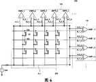
图6是根据本发明的具有集成触摸面板的LCD的第二示例性实施例的部分示意图。在图6中,在第二示例性实施例的TFT阵列面板100的绝缘衬底10上的第一和第二方向上分别形成多条第一和第二传感器线SL1_1至SL1_4和SL2_1至SL2_5。FIG. 6 is a partial schematic diagram of a second exemplary embodiment of an LCD with an integrated touch panel according to the present invention. In FIG. 6 , a plurality of first and second sensor lines SL1_1 to SL1_4 and SL2_1 to SL2_5 are respectively formed in first and second directions on the insulating
沿绝缘衬底10的外围形成第一伪线AL1,以及在第一和第二方向上分别形成第二和第三伪线AL2_1至AL2_4和AL3_1至AL3_5。在该实施例中,将第一伪线AL1连接至第二和第三伪线AL2_1至AL2_4和AL3_1至AL3_5。将参考电压Vref施加给第一、第二、和第三伪线AL1、AL2_1至AL2_4、和AL3_1至AL3_5。A first dummy line AL1 is formed along the periphery of the insulating
将第一和第二传感器线SL1_1至SL1_4和SL2_1至SL2_5分别连接至第一和第二传感器电极28a和63a。The first and second sensor lines SL1_1 to SL1_4 and SL2_1 to SL2_5 are connected to the first and
当将外压施加给显示器的表面时,将形成在共用电极面板200上并位于所施加压力附近的传感器隔离物92电连接至形成在TFT阵列面板100上的第一和第二传感器电极28a和63a,使得将预定电压传输给第一和第二传感器线SL1_1至SL1_4和SL2_1至SL2_5。When external pressure is applied to the surface of the display, the
此外,TFT阵列面板100包括多个第一比较器AMP1_1至AMP1_4以及多个第二比较器AMP2_1至AMP2_5,其中,第一比较器AMP1_1至AMP1_4分别连接至第一传感器线SL1_1至SL1_4和第二伪线AL2_1至AL2_4,并放大每一条第一传感器线SL1_1至SL1_4和每一条第二伪线AL2_1至AL2_4之间的电压差,然后输出放大的电压差,而第二比较器AMP2_1至AMP2_5分别连接至第二传感器线SL2_1至SL2_5和第三伪线AL3_1至AL3_5,并放大每一条第二传感器线SL2_1至SL2_5和每一条第三伪线AL3_1至AL3_5之间的电压差,然后输出放大的电压差。In addition, the
在第二示例性实施例中沿绝缘衬底10的外围形成第一伪线AL1_1以及连接至第一伪线AL1_1的第二和第三伪线AL2_1至AL2_4和AL3_1至AL3_5目的如下。The purpose of forming the first dummy line AL1_1 and the second and third dummy lines AL2_1 to AL2_4 and AL3_1 to AL3_5 connected to the first dummy line AL1_1 along the periphery of the insulating
当第一和第二传感器线SL1_1至SL1_4和SL2_1至SL2_5被与设置在共用电极面板200上的共用电极的耦合所影响时,使第一伪线AL1_1同样被与第一和第二传感器线SL1_1至SL1_4和SL2_1至SL2_5的耦合所影响。因此,第一伪线AL1_1以及第一和第二传感器线SL1_1至SL1_4和SL2_1至SL2_5具有基本相同的相位。因此,根据第二示例性实施例,如上述第一示例性实施例,第一和第二比较器AMP1_1至AMP1_4和AMP2_1至AMP2_5防止了由于通过第一和第二传感器线SL1_1至SL1_4和SL2_1至SL2_5以及第二和第三伪线AL2_1至AL2_4和AL3_1至AL3_5确定相对极性所引起的极性的错误确定。When the first and second sensor lines SL1_1 to SL1_4 and SL2_1 to SL2_5 are affected by coupling with the common electrode provided on the
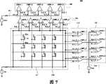
图7是根据本发明的具有集成触摸面板的LCD的第三示例性实施例的部分示意图。在图7的实施例中,在LCD的TFT阵列面板100的绝缘衬底10上的第一和第二方向上形成多条第一和第二传感器线SL1_1至SL1_4和SL2_1至SL2_5。7 is a partial schematic diagram of a third exemplary embodiment of an LCD with an integrated touch panel according to the present invention. In the embodiment of FIG. 7 , a plurality of first and second sensor lines SL1_1 to SL1_4 and SL2_1 to SL2_5 are formed in first and second directions on the insulating
沿绝缘衬底10的外围形成第一伪线AL1,以及在第一和第二方向上分别形成第二和第三伪线AL2_1至AL2_4和AL3_1至AL3_5。在该实施例中,将第一伪线AL1连接至第二和第三伪线AL2_1至AL2_4和AL3_1至AL3_5。将初始电压Vs施加给第一、第二、和第三伪线AL1、AL2_1至AL2_4、和AL3_1至AL3_5,并且初始电压Vs低于共用电压。A first dummy line AL1 is formed along the periphery of the insulating
将第一和第二传感器线SL1_1至SL1_4和SL2_1至SL2_5分别连接至第一和第二传感器电极28a和63a。当将外压施加到显示器的屏幕时,将形成在共用电极面板200上的传感器隔离物92电连接至形成在TFT阵列面板100上的第一和第二传感器电极28a和63a,使得将预定电压传输给第一和第二传感器线SL1_1至SL1_4和SL2_1至SL2_5。The first and second sensor lines SL1_1 to SL1_4 and SL2_1 to SL2_5 are connected to the first and
TFT阵列面板100包括多个第一比较器AMP1_1至AMP1_4以及多个第二比较器AMP2_1至AMP2_5,其中,第一比较器AMP1_1至AMP1_4分别连接至第一传感器线SL1_1至SL1_4和第二伪线AL2_1至AL2_4,并放大每一条第一传感器线SL1_1至SL1_4和每一条第二伪线AL2_1至AL2_4之间的电压差,然后输出放大的电压差,而第二比较器AMP2_1至AMP2_5分别连接至第二传感器线SL2_1至SL2_5和第三伪线AL3_1至AL3_5,并放大每一条第二传感器线SL2_1至SL2_5和每一条第三伪线AL3_1至AL3_5之间的电压差,然后输出放大的电压差。The
此外,TFT阵列面板100包括多个第三比较器AMP3_1至AMP3_4以及多个第四比较器AMP4_1至AMP4_5,其中,第三比较器AMP3_1至AMP3_4分别连接至第一比较器AMP1_1至AMP1_4的输出端OL1_1至OL1_4和第四伪线AL4_1至AL4_4,并放大每个输出端OL1_1至OL1_4和每一条第四伪线AL4_1至AL4_4之间的电压差,然后输出放大的电压差,而第四比较器AMP4_1至AMP4_5分别连接至第二比较器AMP2_1至AMP2_5的输出端OL2_1至OL2_5和第五伪线AL5_1至AL5_5,并放大每个输出端OL2_1至OL2_5和每一条第五伪线AL5_1至AL5_5之间的电压差,然后输出放大的电压差。这里,将参考电压Vref施加给第四和第五伪线AL4_1至AL4_4和AL5_1至AL5_5。In addition, the
根据作为第二实施例修改的第三示例性实施例,将已经施加给第一和第二传感器线SL1_1至SL1_4和SL2_1至SL2_5的初始电压施加给第一、第二、和第三伪线AL1、AL2_1至AL2_4、和AL3_1至AL3_5,并将第三和第四比较器AMP3_1至AMP3_4和AMP4_1至AMP4_5分别连接至第一和第二比较器AMP1_1至AMP1_4和AMP2_1至AMP2_5的输出端。上述配置的目的如下。According to the third exemplary embodiment as a modification of the second embodiment, the initial voltages already applied to the first and second sensor lines SL1_1 to SL1_4 and SL2_1 to SL2_5 are applied to the first, second, and third dummy lines AL1 , AL2_1 to AL2_4, and AL3_1 to AL3_5, and the third and fourth comparators AMP3_1 to AMP3_4 and AMP4_1 to AMP4_5 are respectively connected to the output terminals of the first and second comparators AMP1_1 to AMP1_4 and AMP2_1 to AMP2_5. The purpose of the above configuration is as follows.
当将已经施加给第一和第二传感器线SL1_1至SL1_4和SL2_1至SL2_5的初始电压Vs施加给第一、第二、和第三伪线AL1、AL2_1至AL2_4、和AL3_1至AL3_5时,施加给第一和第二传感器线SL1_1至SL1_4和SL2_1至SL2_5的电压与施加给第一、第二、和第三伪线AL1、AL2_1至AL2_4、和AL3_1至AL3_5的电压相等。When the initial voltage Vs that has been applied to the first and second sensor lines SL1_1 to SL1_4 and SL2_1 to SL2_5 is applied to the first, second, and third dummy lines AL1, AL2_1 to AL2_4, and AL3_1 to AL3_5, the Voltages of the first and second sensor lines SL1_1 to SL1_4 and SL2_1 to SL2_5 are equal to voltages applied to the first, second, and third dummy lines AL1 , AL2_1 to AL2_4 , and AL3_1 to AL3_5 .
换句话说,当没有对显示器施加外压时,将相同的电压施加给第一和第二传感器线SL1_1至SL1_4和SL2_1至SL2_5以及第一、第二、和第三伪线AL1、AL2_1至AL2_4、和AL3_1至AL3_5,使得第一和第二比较器AMP1_1至AMP1_4和AMP2_1至AMP2_5的输出为‘0’。In other words, when no external pressure is applied to the display, the same voltage is applied to the first and second sensor lines SL1_1 to SL1_4 and SL2_1 to SL2_5 and the first, second, and third dummy lines AL1, AL2_1 to AL2_4 , and AL3_1 to AL3_5, so that the outputs of the first and second comparators AMP1_1 to AMP1_4 and AMP2_1 to AMP2_5 are '0'.
此外,当将外压施加给显示器时,将预定电压施加给第一和第二传感器线SL1_1至SL1_4和SL2_1至SL2_5,使得第一和第二比较器AMP1_1至AMP1_4和AMP2_1至AMP2_5输出高电平信号,然后将高电平信号输入至第三和第四比较器AMP3_1至AMP3_4和AMP4_1至AMP4_5。然后,第三和第四比较器AMP3_1至AMP3_4和AMP4_1至AMP4_5将输出的高电平信号与参考电压Vref进行比较,并输出高电平信号。因此,由于第一和第二传感器线SL1_1至SL1_4和SL2_1至SL2_5没有被来自共用电极面板200的共用电极的耦合所影响,所以可以有效地消除在第一和第二传感器线SL1_1至SL1_4和SL2_1至SL2_5中发生的耦合噪声。In addition, when an external pressure is applied to the display, a predetermined voltage is applied to the first and second sensor lines SL1_1 to SL1_4 and SL2_1 to SL2_5 so that the first and second comparators AMP1_1 to AMP1_4 and AMP2_1 to AMP2_5 output a high level signal, and then input the high-level signal to the third and fourth comparators AMP3_1 to AMP3_4 and AMP4_1 to AMP4_5. Then, the third and fourth comparators AMP3_1 to AMP3_4 and AMP4_1 to AMP4_5 compare the output high level signal with the reference voltage Vref and output a high level signal. Therefore, since the first and second sensor lines SL1_1 to SL1_4 and SL2_1 to SL2_5 are not affected by the coupling from the common electrode of the
图8是根据本发明的具有集成触摸面板的LCD的第四示例性实施例的部分示意图。在图8的示例性LCD中,在LCD的TFT阵列面板100的绝缘衬底10上的第一和第二方向上形成多条第一和第二传感器线SL1_1至SL1_4和SL2_1至SL2_5。FIG. 8 is a partial schematic view of a fourth exemplary embodiment of an LCD with an integrated touch panel according to the present invention. In the exemplary LCD of FIG. 8 , a plurality of first and second sensor lines SL1_1 to SL1_4 and SL2_1 to SL2_5 are formed in first and second directions on the insulating
沿绝缘衬底10的外围形成第一伪线AL1,以及在与第一和第二传感器线SL1_1至SL1_4和SL2_1至SL2_5相同的方向上分别形成多条第二和第三伪线AL2_1至AL2_4和AL3_1至AL3_5。在该实施例中,将第一伪线AL_1连接至第二和第三伪线AL2_1至AL2_4和AL3_1至AL3_5。将初始电压Vs施加给第一、第二、和第三伪线AL1、AL2_1至AL2_4、和AL3_1至AL3_5,初始电压低于共用电压。A first dummy line AL1 is formed along the periphery of the insulating
将第一和第二传感器线SL1_1至SL1_4和SL2_1至SL2_5分别连接至第一和第二传感器电极28a和63a。当将外压施加到显示器时,将形成在共用电极面板200上的传感器隔离物92电连接至形成在TFT阵列面板100上的第一和第二传感器电极28a和63a,使得将预定电压传输给第一和第二传感器线SL1_1至SL1_4和SL2_1至SL2_5。The first and second sensor lines SL1_1 to SL1_4 and SL2_1 to SL2_5 are connected to the first and
TFT阵列面板100包括多个第一比较器AMP1_1至AMP1_4以及多个第二比较器AMP2_1至AMP2_5,其中,第一比较器AMP1_1至AMP1_4分别连接至第一传感器线SL1_1至SL1_4和第二伪线AL2_1至AL2_4,并放大每条第一传感器线SL1_1至SL1_4和每条第二伪线AL2_1至AL2_4之间的电压差,然后输出放大的电压差,而第二比较器AMP2_1至AMP2_5分别连接至第二传感器线SL2_1至SL2_5和第三伪线AL3_1至AL3_5,并放大每条第二传感器线SL2_1至SL2_5和每条第三伪线AL3_1至AL3_5之间的电压差,然后输出放大的电压差。The
此外,TFT阵列面板100包括多个第三比较器AMP3_1至AMP3_4以及多个第四比较器AMP4_1至AMP4_5,其中,第三比较器AMP3_1至AMP3_4分别连接至第一比较器AMP1_1至AMP1_4的输出端OL1_1至OL1_4和第四伪线AL4_1至AL4_4,并放大每个输出端OL1_1至OL1_4和每条第四伪线AL4_1至AL4_4之间的电压差,然后输出放大的电压差,而第四比较器AMP4_1至AMP4_5分别连接至第二比较器AMP2_1至AMP2_5的输出端OL2_1至OL2_5和第五伪线AL5_1至AL5_5,并放大每个输出端OL2_1至OL2_5和每条第五伪线AL5_1至AL5_5之间的电压差,然后输出放大的电压差。这里,将参考电压Vref施加给第四和第五伪线AL4_1至AL4_4和AL5_1至AL5_5。In addition, the
第四示例性LCD是图7的第三示例性实施例的修改,并具有与第三实施例基本相同的配置,除了在与S1_1至SL1_4和SL2_1至SL2_5相同的方向上分别形成的第二和第三伪线AL2_1至AL2_4和AL3_1至AL3_5被形成为分别与第二和第一传感器线SL2_1至SL2_5和SL1_1至SL1_4交叉。因此,第四示例性实施例与上述本发明的第三示例性实施例进行相似的操作并实现基本相同的优点。The fourth exemplary LCD is a modification of the third exemplary embodiment of FIG. 7, and has substantially the same configuration as the third embodiment, except that the second and The third dummy lines AL2_1 to AL2_4 and AL3_1 to AL3_5 are formed to cross the second and first sensor lines SL2_1 to SL2_5 and SL1_1 to SL1_4, respectively. Therefore, the fourth exemplary embodiment performs similar operations and achieves substantially the same advantages as the third exemplary embodiment of the present invention described above.
图9是根据本发明的具有集成触摸面板的LCD第五示例性实施例的部分示意图。在图9的示例性实施例中,在LCD的TFT阵列面板100的绝缘衬底10上的第一和第二方向上形成多条第一和第二传感器线SL1_1至SL1_4和SL2_1至SL2_5。9 is a partial schematic diagram of a fifth exemplary embodiment of an LCD with an integrated touch panel according to the present invention. In the exemplary embodiment of FIG. 9 , a plurality of first and second sensor lines SL1_1 to SL1_4 and SL2_1 to SL2_5 are formed in first and second directions on the insulating
在第一和第二方向上形成多条第一和第二伪线AL1_1至AL1_4和AL2_1至AL2_5,并将第三伪线AL3分别连接至第一和第二伪线AL1_1至AL1_4和AL2_1至AL2_5。这里,将参考电压Vref施加给第一、第二、和第三伪线AL1_1至AL1_4、AL2_1至AL2_5、和AL3。Form a plurality of first and second dummy wires AL1_1 to AL1_4 and AL2_1 to AL2_5 in the first and second directions, and connect the third dummy wire AL3 to the first and second dummy wires AL1_1 to AL1_4 and AL2_1 to AL2_5, respectively . Here, the reference voltage Vref is applied to the first, second, and third dummy lines AL1_1 to AL1_4 , AL2_1 to AL2_5 , and AL3 .
将第一和第二传感器线SL1_1至SL1_4和SL2_1至SL2_5分别连接至第一和第二传感器电极28a和63a。当将外压施加到显示器时,将形成在共用电极面板200上的传感器隔离物92电连接至形成在TFT阵列面板100上的第一和第二传感器电极28a和63a,使得将预定电压传输给第一和第二传感器线SL1_1至SL1_4和SL2_1至SL2_5。The first and second sensor lines SL1_1 to SL1_4 and SL2_1 to SL2_5 are connected to the first and
此外,TFT阵列面板100包括多个第一比较器AMP1_1至AMP1_4以及多个第二比较器AMP2_1至AMP2_5,其中,第一比较器AMP1_1至AMP1_4分别连接至第一传感器线SL1_1至SL1_4和第一伪线AL1_1至AL1_4,并放大每条第一传感器线SL1_1至SL1_4和每条第一伪线AL1_1至AL1_4之间的电压差,然后输出放大的电压差,而第二比较器AMP2_1至AMP2_5分别连接至第二传感器线SL2_1至SL2_5和第二伪线AL2_1至AL2_5,并放大每条第二传感器线SL2_1至SL2_5和每条第二伪线AL2_1至AL2_5之间的电压差,然后输出放大的电压差。In addition, the
在图9的第五示例性实施例中,将TFT阵列面板100连接至其上安装有多个用于驱动TFT的部件的印刷电路板300。如图9中所示,印刷电路板300包括:第一互连线311,通过其将预定电压施加给第一、第二、和第三伪线AL1_1至AL1_4、AL2_1至AL2_5、和AL3;第二互连线313,通过其将栅极截止电压Voff施加给栅极线GL1至GLn;栅极驱动器320,从第二互连线313接收栅极截止电压Voff,并顺序将栅极截止电压Voff施加给栅极线GL1至GLn;以及电容器C1,耦合在第一互连线311和第二互连线313之间,用于消除发生在其间的耦合噪声。将参考电压Vref施加给第一互连线311。In the fifth exemplary embodiment of FIG. 9, the
为了下列原因,将本发明的第五示例性实施例的电容器C1设置在第一互连线311和第二互连线313之间。The capacitor C1 of the fifth exemplary embodiment of the present invention is provided between the first interconnection line 311 and the second interconnection line 313 for the following reasons.
将栅极截止电压Voff施加给连接至栅极驱动器320的栅极线GL1至GLn,不包括已经施加有栅极导通电压Von的栅极线GL1至GLn。这里,由于形成在TFT阵列面板100上的数据线和形成在共用电极面板200上的共用电极之间的耦合,共用电压可能失真。在这种情况下,一旦将栅极截止电压Voff施加给栅极线GL1至GLn,该电压还与共用电极或数据线耦合。The gate-off voltage Voff is applied to the gate lines GL1 to GLn connected to the gate driver 320 excluding the gate lines GL1 to GLn to which the gate-on voltage Von has been applied. Here, the common voltage may be distorted due to coupling between the data lines formed on the
为了解决这个问题,将电容器C1设置在第一互连线311和第二互连线313之间,以电平移动提供给参考电压Vref的电平的栅极截止电压Voff,从而将参考电压Vref施加给第一、第二、和第三伪线AL1_1至AL1_4、AL2_1至AL2_5、和AL3。因此,第一和第二传感器线SL1_1至SL1_4和SL2_1至SL2_5以及第一和第二伪线AL1_1至AL1_4和AL2_1至AL2_5具有基本相同的相位。因此,在第五示例性实施例中,防止了第一和第二比较器AMP1_1至AMP1_4和AMP2_1至AMP2_5做出由于通过第一和第二传感器线SL1_1至SL1_4和SL2_1至SL2_5以及第一和第二伪线AL1_1至AL1_4和AL2_1至AL2_5确定相对极性所引起的错误的极性确定。In order to solve this problem, a capacitor C1 is provided between the first interconnection line 311 and the second interconnection line 313 to level-shift the gate-off voltage Voff supplied to the level of the reference voltage Vref, thereby changing the reference voltage Vref Applied to the first, second, and third dummy wires AL1_1 to AL1_4, AL2_1 to AL2_5, and AL3. Accordingly, the first and second sensor lines SL1_1 to SL1_4 and SL2_1 to SL2_5 and the first and second dummy lines AL1_1 to AL1_4 and AL2_1 to AL2_5 have substantially the same phase. Therefore, in the fifth exemplary embodiment, the first and second comparators AMP1_1 to AMP1_4 and AMP2_1 to AMP2_5 are prevented from making due to the first and second sensor lines SL1_1 to SL1_4 and SL2_1 to SL2_5 and the The two pseudowires AL1_1 to AL1_4 and AL2_1 to AL2_5 determine relative polarity causing erroneous polarity determination.
虽然第五示例性实施例描述并示出了将参考电压Vref施加给第一、第二、和第三伪线AL1_1至AL1_4、AL2_1至AL2_5、和AL3,但本发明不限于示出和描述的具体实例,而是还可以将已经施加给第一和第二传感器线SL1_1至SL1_4和SL2_1至SL2_5的初始电压Vs施加给第一、第二、和第三伪线AL1_1至AL1_4、AL2_1至AL2_5、和AL3。在这种情况下,可使用与第四示例性实施例具有相同配置的比较器,即,可使用包括第一至第四比较器的比较器。Although the fifth exemplary embodiment describes and shows that the reference voltage Vref is applied to the first, second, and third dummy lines AL1_1 to AL1_4, AL2_1 to AL2_5, and AL3, the present invention is not limited to the shown and described As a specific example, it is also possible to apply the initial voltage Vs already applied to the first and second sensor lines SL1_1 to SL1_4 and SL2_1 to SL2_5 to the first, second, and third pseudo lines AL1_1 to AL1_4, AL2_1 to AL2_5, and AL3. In this case, comparators having the same configuration as the fourth exemplary embodiment, that is, comparators including the first to fourth comparators can be used.
根据本文描述的示例性实施例,通过消除耦合噪声防止显示器触摸面板传感器故障。According to exemplary embodiments described herein, display touch panel sensor failure is prevented by eliminating coupling noise.
虽然参照本发明的示例性实施例具体示出并描述了本发明,但本领域普通技术人员应该理解,在不背离如下面权利要求限定的本发明的精神和范围的情况下,可在形式和细节上做出各种改变。因此,期望本发明的实施例在各个方面被认为是示例性的而不是限制性的,对所附权利要求和其功能等价物作出参考而不是用前述描述来表示本发明的范围。While the invention has been particularly shown and described with reference to exemplary embodiments thereof, it should be understood by those of ordinary skill in the art that changes may be made in form and form without departing from the spirit and scope of the invention as defined in the following claims. Various changes were made in the details. It is therefore intended that the embodiments of the invention be considered in all respects as illustrative rather than restrictive, and that reference is made to the appended claims and their functional equivalents rather than the foregoing description as indicating the scope of the invention.
Claims (16)
Applications Claiming Priority (3)
| Application Number | Priority Date | Filing Date | Title |
|---|---|---|---|
| KR1020060110515AKR101297387B1 (en) | 2006-11-09 | 2006-11-09 | Liquid crystal display associated with touch panel |
| KR1020060110515 | 2006-11-09 | ||
| KR10-2006-0110515 | 2006-11-09 |
Publications (2)
| Publication Number | Publication Date |
|---|---|
| CN101178524A CN101178524A (en) | 2008-05-14 |
| CN101178524Btrue CN101178524B (en) | 2011-05-11 |
Family
ID=39000685
Family Applications (1)
| Application Number | Title | Priority Date | Filing Date |
|---|---|---|---|
| CN2007101651936AExpired - Fee RelatedCN101178524B (en) | 2006-11-09 | 2007-11-08 | LCDs with integrated touch panels |
Country Status (5)
| Country | Link |
|---|---|
| US (2) | US8493518B2 (en) |
| EP (1) | EP1921537B1 (en) |
| JP (1) | JP5350606B2 (en) |
| KR (1) | KR101297387B1 (en) |
| CN (1) | CN101178524B (en) |
Families Citing this family (117)
| Publication number | Priority date | Publication date | Assignee | Title |
|---|---|---|---|---|
| US7663607B2 (en) | 2004-05-06 | 2010-02-16 | Apple Inc. | Multipoint touchscreen |
| KR101246830B1 (en)* | 2006-06-09 | 2013-03-28 | 삼성디스플레이 주식회사 | Display device and method of driving the same |
| US20070283832A1 (en)* | 2006-06-09 | 2007-12-13 | Apple Computer, Inc. | Imprint circuit patterning |
| US8259078B2 (en)* | 2006-06-09 | 2012-09-04 | Apple Inc. | Touch screen liquid crystal display |
| CN102981678B (en) | 2006-06-09 | 2015-07-22 | 苹果公司 | Touch screen liquid crystal display |
| CN104965621B (en) | 2006-06-09 | 2018-06-12 | 苹果公司 | Touch screen LCD and its operating method |
| US7812827B2 (en)* | 2007-01-03 | 2010-10-12 | Apple Inc. | Simultaneous sensing arrangement |
| US8493330B2 (en) | 2007-01-03 | 2013-07-23 | Apple Inc. | Individual channel phase delay scheme |
| US9710095B2 (en) | 2007-01-05 | 2017-07-18 | Apple Inc. | Touch screen stack-ups |
| KR101383708B1 (en)* | 2007-03-27 | 2014-04-10 | 삼성디스플레이 주식회사 | Display device and manufactuing method of the same |
| US8493331B2 (en) | 2007-06-13 | 2013-07-23 | Apple Inc. | Touch detection using multiple simultaneous frequencies |
| KR101451938B1 (en)* | 2008-03-17 | 2014-10-17 | 삼성디스플레이 주식회사 | Display panel with a built-in touch screen |
| CN101939693B (en)* | 2008-03-21 | 2012-02-29 | 夏普株式会社 | Liquid crystal display device with built-in touch sensor |
| TWI379228B (en)* | 2008-04-18 | 2012-12-11 | Au Optronics Corp | Resistance type touch display panel |
| RU2457550C1 (en)* | 2008-06-03 | 2012-07-27 | Шарп Кабусики Кайся | Display device |
| KR101483626B1 (en)* | 2008-06-09 | 2015-01-16 | 삼성디스플레이 주식회사 | Touch screen display device |
| JP5154316B2 (en)* | 2008-06-30 | 2013-02-27 | 株式会社ジャパンディスプレイイースト | Touch panel |
| US8508495B2 (en) | 2008-07-03 | 2013-08-13 | Apple Inc. | Display with dual-function capacitive elements |
| TWI375485B (en)* | 2008-07-04 | 2012-10-21 | Au Optronics Corp | Electroluminescent display touch panel |
| WO2010007890A1 (en)* | 2008-07-16 | 2010-01-21 | シャープ株式会社 | Display device |
| CN101666931B (en)* | 2008-09-05 | 2011-12-28 | 北京京东方光电科技有限公司 | Liquid crystal display (LCD), TFT-LCD array substrate and manufacturing method thereof |
| US9348451B2 (en) | 2008-09-10 | 2016-05-24 | Apple Inc. | Channel scan architecture for multiple stimulus multi-touch sensor panels |
| US8592697B2 (en) | 2008-09-10 | 2013-11-26 | Apple Inc. | Single-chip multi-stimulus sensor controller |
| US9606663B2 (en) | 2008-09-10 | 2017-03-28 | Apple Inc. | Multiple stimulation phase determination |
| JP5467449B2 (en)* | 2008-09-17 | 2014-04-09 | Nltテクノロジー株式会社 | Lead wire wiring device, image display device, and lead wire wiring device manufacturing method |
| US9927924B2 (en)* | 2008-09-26 | 2018-03-27 | Apple Inc. | Differential sensing for a touch panel |
| KR101564332B1 (en) | 2008-10-28 | 2015-10-30 | 삼성전자주식회사 | Touch screen panel integrated into a liquid crystal display, manufacturing method thereof, and touch sensing method |
| TWI383312B (en)* | 2008-11-13 | 2013-01-21 | Orise Technology Co Ltd | Method for detecting touch point and touch panel using the same |
| US8144295B2 (en) | 2008-11-18 | 2012-03-27 | Apple Inc. | Common bus design for a TFT-LCD display |
| KR101310378B1 (en)* | 2008-11-19 | 2013-09-23 | 엘지디스플레이 주식회사 | Liquid crystal display |
| TWI380108B (en)* | 2008-11-28 | 2012-12-21 | Au Optronics Corp | Display panel with multi-touch function |
| US8749496B2 (en) | 2008-12-05 | 2014-06-10 | Apple Inc. | Integrated touch panel for a TFT display |
| KR101525802B1 (en)* | 2008-12-11 | 2015-06-11 | 삼성디스플레이 주식회사 | Liquid crystal display |
| KR101521096B1 (en)* | 2008-12-19 | 2015-05-18 | 삼성디스플레이 주식회사 | Display device |
| KR101587889B1 (en)* | 2009-01-23 | 2016-01-25 | 삼성디스플레이 주식회사 | Display panel and manufacturing method thereof |
| WO2010084642A1 (en) | 2009-01-26 | 2010-07-29 | シャープ株式会社 | Touch panel incorporated into display device |
| US8217913B2 (en) | 2009-02-02 | 2012-07-10 | Apple Inc. | Integrated touch screen |
| US7995041B2 (en)* | 2009-02-02 | 2011-08-09 | Apple Inc. | Integrated touch screen |
| US8531432B2 (en) | 2009-02-18 | 2013-09-10 | Sharp Kabushiki Kaisha | Touch panel with built-in display device |
| CN101825787B (en)* | 2009-03-04 | 2013-06-12 | 北京京东方光电科技有限公司 | Touch display screen and manufacture method thereof |
| US20120013593A1 (en)* | 2009-03-17 | 2012-01-19 | Sharp Kabushiki Kaisha | Display device |
| JP4900421B2 (en)* | 2009-05-29 | 2012-03-21 | カシオ計算機株式会社 | Liquid crystal display panel and liquid crystal display device |
| JP2012177953A (en)* | 2009-06-30 | 2012-09-13 | Sharp Corp | Optical sensor and display device |
| TWI421741B (en)* | 2009-07-01 | 2014-01-01 | Au Optronics Corp | Touch panel and sensing method thereof |
| KR101082294B1 (en)* | 2009-09-04 | 2011-11-09 | 삼성모바일디스플레이주식회사 | flat panel display integrated touch screen panel |
| KR101657215B1 (en) | 2009-09-08 | 2016-09-19 | 삼성디스플레이 주식회사 | Display device including touch panel device and coupling-noise elliminating method |
| KR101588347B1 (en) | 2009-09-28 | 2016-01-26 | 삼성디스플레이 주식회사 | Liquid crystal display panel, liquid crystal display device including same, and driving method of liquid crystal display device |
| CN102231090B (en) | 2009-10-22 | 2014-03-12 | 群康科技(深圳)有限公司 | Touch display panel and touch display device |
| TWI417860B (en)* | 2009-11-05 | 2013-12-01 | Innolux Display Corp | Touch panel and touch display device |
| US20110134051A1 (en)* | 2009-12-08 | 2011-06-09 | Holylite Microelectronics Corp. | Liquid crystal display system integrated with touch detector |
| CN102667679A (en)* | 2009-12-28 | 2012-09-12 | 夏普株式会社 | Display device |
| JP2011170616A (en)* | 2010-02-18 | 2011-09-01 | On Semiconductor Trading Ltd | Capacitance type touch sensor |
| US9201259B2 (en)* | 2010-03-19 | 2015-12-01 | Lg Display Co., Ltd. | Touch sensing type liquid crystal display device and method of fabricating the same |
| CN102834795A (en)* | 2010-03-29 | 2012-12-19 | 夏普株式会社 | Display device having touch panel functionality |
| CN102834793A (en)* | 2010-03-29 | 2012-12-19 | 夏普株式会社 | Display device with touch panel functionality |
| JP2013140190A (en)* | 2010-04-21 | 2013-07-18 | Sharp Corp | Display device |
| US8449818B2 (en)* | 2010-06-30 | 2013-05-28 | H. C. Starck, Inc. | Molybdenum containing targets |
| CN102314389B (en)* | 2010-07-08 | 2015-04-15 | 飞思卡尔半导体公司 | Method for detecting failure of touch sensor interface and system |
| JP5500013B2 (en) | 2010-09-08 | 2014-05-21 | カシオ計算機株式会社 | Touch-type liquid crystal display device with built-in contacts |
| JP5573540B2 (en)* | 2010-09-22 | 2014-08-20 | カシオ計算機株式会社 | Touch panel |
| KR101848063B1 (en) | 2010-11-17 | 2018-04-12 | 삼성디스플레이 주식회사 | Liquid crystal display device and method of fabricating the same |
| US8804056B2 (en) | 2010-12-22 | 2014-08-12 | Apple Inc. | Integrated touch screens |
| TWI452505B (en)* | 2011-01-25 | 2014-09-11 | Touch screen display | |
| TWI471796B (en)* | 2011-02-11 | 2015-02-01 | Wintek Corp | Touch-sensitive display device |
| TWI443570B (en)* | 2011-04-01 | 2014-07-01 | Raydium Semiconductor Corp | Ungrounded touch input device and control device thereof |
| KR101726640B1 (en)* | 2011-04-13 | 2017-04-14 | 엘지디스플레이 주식회사 | In cell type touch display device and method for compensating touch data using the same |
| CN103135815B (en)* | 2011-11-25 | 2017-02-22 | 上海天马微电子有限公司 | Liquid crystal display device with embedded touch screen and touch control driving method thereof |
| KR101893111B1 (en)* | 2012-01-04 | 2018-08-31 | 삼성디스플레이 주식회사 | Display device including sensor |
| KR101378511B1 (en)* | 2012-03-28 | 2014-03-27 | 주식회사 하이딥 | Method, touch sensing apparatus and computer-readable recording medium for minimizing noise on touch panel |
| KR101315227B1 (en) | 2012-05-30 | 2013-10-07 | 엘지디스플레이 주식회사 | Display device with integrated touch screen and method for driving the same |
| US9395583B2 (en) | 2012-06-06 | 2016-07-19 | Apple Inc. | Column spacer design for a display incorporating a third metal layer |
| KR101996951B1 (en)* | 2012-06-26 | 2019-07-08 | 엘지이노텍 주식회사 | Touch panel, position sensing method of touch panel and integrated circuit |
| WO2014003225A1 (en)* | 2012-06-25 | 2014-01-03 | Lg Innotek Co., Ltd. | Touch panel, position sensing method of touch panel, and integrated circuit |
| KR101996955B1 (en)* | 2012-06-25 | 2019-07-08 | 엘지이노텍 주식회사 | Touch panel, position sensing method of touch panel and integrated circuit |
| KR102042019B1 (en)* | 2012-06-25 | 2019-11-08 | 엘지이노텍 주식회사 | Touch panel, position sensing method of touch panel and integrated circuit |
| KR20140012803A (en)* | 2012-07-23 | 2014-02-04 | 삼성디스플레이 주식회사 | Display panel and method of driving the same |
| GB2505175B (en)* | 2012-08-20 | 2020-02-05 | Flexenable Ltd | Forming a conductive connection between a common electrode of an optical media component and a electrical contact of a control component |
| JP5778119B2 (en) | 2012-11-30 | 2015-09-16 | 株式会社ジャパンディスプレイ | Display device with touch detection function and electronic device |
| US20140218302A1 (en)* | 2013-02-01 | 2014-08-07 | MiSeat, Inc. | Touch and tap operable work surface |
| US9336723B2 (en) | 2013-02-13 | 2016-05-10 | Apple Inc. | In-cell touch for LED |
| KR102135908B1 (en)* | 2013-06-26 | 2020-07-21 | 엘지디스플레이 주식회사 | Touch sensing apparatus and method for driving the same |
| KR102111625B1 (en)* | 2013-06-28 | 2020-05-18 | 삼성디스플레이 주식회사 | Display device having touch sensor and manufacturing method thereof |
| CN103558946A (en)* | 2013-11-15 | 2014-02-05 | 京东方科技集团股份有限公司 | Touch structure, liquid crystal panel and display device |
| KR102082265B1 (en)* | 2013-11-28 | 2020-02-27 | 엘지디스플레이 주식회사 | Touch sensor integrated type display device |
| CN116560524B (en) | 2013-12-13 | 2024-10-01 | 苹果公司 | Integrated touch and display architecture for self-capacitance touch sensor |
| JP2015143933A (en)* | 2014-01-31 | 2015-08-06 | 株式会社ジャパンディスプレイ | Display device with capacitance sensor and driving method therefor |
| EP3130984B1 (en)* | 2014-04-07 | 2019-09-04 | Murata Manufacturing Co., Ltd. | Touch panel and electronic device |
| WO2015160377A1 (en) | 2014-04-16 | 2015-10-22 | Wrostix Technologies Llc | Structure for pixelated self-capacitance |
| US9841855B2 (en)* | 2014-04-25 | 2017-12-12 | Marvell World Trade Ltd. | Systems and methods for capacitive touch detection |
| US10133382B2 (en) | 2014-05-16 | 2018-11-20 | Apple Inc. | Structure for integrated touch screen |
| US9367188B2 (en) | 2014-05-23 | 2016-06-14 | Apple Inc. | RC matching in a touch screen |
| WO2015183334A1 (en) | 2014-05-28 | 2015-12-03 | Pylemta Management Llc | Narrow border touch screen |
| KR101655410B1 (en) | 2014-08-26 | 2016-09-07 | 엘지디스플레이 주식회사 | In-cell Touch type liquid crystal display device |
| KR102274701B1 (en)* | 2014-12-29 | 2021-07-08 | 엘지디스플레이 주식회사 | Pad structure and display device having the same |
| CN106033765B (en)* | 2015-03-17 | 2019-06-11 | 上海和辉光电有限公司 | Organic Light Emitting Diode touch-control display panel |
| US9817506B2 (en)* | 2015-03-31 | 2017-11-14 | Synaptics Incorporated | Sensor array configurations for differential readout |
| CN104834406B (en) | 2015-05-29 | 2018-09-18 | 京东方科技集团股份有限公司 | A kind of display device and its driving method of integrated touch function |
| KR20170003041A (en) | 2015-06-30 | 2017-01-09 | 삼성전자주식회사 | Device for Determining Effective User Input |
| US9946403B2 (en)* | 2015-08-31 | 2018-04-17 | Lg Display Co., Ltd. | Display device, method for driving the same, and driving circuit thereof |
| KR102410726B1 (en)* | 2015-09-30 | 2022-06-20 | 엘지디스플레이 주식회사 | In-cell touch type display device |
| KR102554251B1 (en)* | 2015-12-07 | 2023-07-11 | 엘지디스플레이 주식회사 | Display device |
| CN105824469B (en)* | 2016-03-15 | 2018-10-30 | 京东方科技集团股份有限公司 | A kind of display base plate, In-cell touch panel and display device |
| TWI581169B (en)* | 2016-04-28 | 2017-05-01 | 友達光電股份有限公司 | Dual-mode capacitive touch display panel |
| KR101964934B1 (en) | 2016-07-29 | 2019-04-04 | 삼성디스플레이 주식회사 | Display device and method for fabricating the same |
| CN106054468A (en)* | 2016-07-29 | 2016-10-26 | 厦门天马微电子有限公司 | Display panel and display device comprising same |
| CN106157891B (en)* | 2016-08-15 | 2018-10-12 | 京东方科技集团股份有限公司 | A kind of lines identification display device |
| WO2018043588A1 (en)* | 2016-08-30 | 2018-03-08 | シャープ株式会社 | Capacitance type touch panel with built-in pressure sensor |
| CN106293257B (en)* | 2016-10-10 | 2019-02-01 | 南京中电熊猫液晶显示科技有限公司 | In-cell touch panel and detection method thereof |
| KR102603269B1 (en)* | 2016-10-24 | 2023-11-17 | 삼성전자주식회사 | electronic device including pressure sensor |
| KR102707589B1 (en)* | 2016-11-29 | 2024-09-20 | 엘지디스플레이 주식회사 | Touch Display Device, Display Panel, Touch Sensing Method, Touch Sensing Circuit, and Driving Circuit |
| KR102662681B1 (en) | 2016-12-26 | 2024-04-30 | 엘지디스플레이 주식회사 | Display device with integrated touch screen and method for fabricating the same |
| TWI648800B (en)* | 2017-08-03 | 2019-01-21 | 友達光電股份有限公司 | Pixel structure |
| US10845902B2 (en)* | 2018-03-30 | 2020-11-24 | Sharp Kabushiki Kaisha | Touch sensor for display |
| KR102584437B1 (en)* | 2018-07-24 | 2023-09-27 | 엘지디스플레이 주식회사 | Display device |
| US11367390B2 (en)* | 2018-12-24 | 2022-06-21 | Novatek Microelectronics Corp. | Display apparatus and method for noise reduction |
| KR102803986B1 (en)* | 2019-04-15 | 2025-05-12 | 삼성디스플레이 주식회사 | Display device |
| KR102848816B1 (en)* | 2020-06-01 | 2025-08-25 | 삼성디스플레이 주식회사 | Display device |
Citations (1)
| Publication number | Priority date | Publication date | Assignee | Title |
|---|---|---|---|---|
| CN1534333A (en)* | 2003-03-28 | 2004-10-06 | Lg.飞利浦Lcd有限公司 | Liquid crystal display device with electromagnetic type touch screen |
Family Cites Families (29)
| Publication number | Priority date | Publication date | Assignee | Title |
|---|---|---|---|---|
| JPS59192765U (en)* | 1983-06-06 | 1984-12-21 | 株式会社 写研 | Noise removal structure of tablet input device |
| JPH0255323U (en)* | 1988-10-11 | 1990-04-20 | ||
| US5305017A (en)* | 1989-08-16 | 1994-04-19 | Gerpheide George E | Methods and apparatus for data input |
| JPH056153A (en)* | 1991-06-27 | 1993-01-14 | Alps Electric Co Ltd | Liquid crystal display device with touch panel |
| JPH05224818A (en) | 1992-02-10 | 1993-09-03 | Matsushita Electric Ind Co Ltd | Touch panel device |
| GB9209364D0 (en) | 1992-04-30 | 1992-06-17 | Varitronix Ltd | A touch sensitive device |
| US5565658A (en) | 1992-07-13 | 1996-10-15 | Cirque Corporation | Capacitance-based proximity with interference rejection apparatus and methods |
| JP3170051B2 (en) | 1992-07-21 | 2001-05-28 | ローム株式会社 | Liquid crystal display |
| GB2295712B (en) | 1994-12-03 | 1998-06-17 | Icl Systems Ab | Theft protection for electrically-powered articles |
| US5777596A (en)* | 1995-11-13 | 1998-07-07 | Symbios, Inc. | Touch sensitive flat panel display |
| US5995172A (en)* | 1997-01-02 | 1999-11-30 | Nec Corporation | Tablet integrated liquid crystal display apparatus with less parallax |
| US5872561A (en)* | 1997-03-31 | 1999-02-16 | Allen-Bradley Company, Llc | Fast scanning switch matrix |
| JP4044187B2 (en)* | 1997-10-20 | 2008-02-06 | 株式会社半導体エネルギー研究所 | Active matrix display device and manufacturing method thereof |
| KR100595922B1 (en)* | 1998-01-26 | 2006-07-05 | 웨인 웨스터만 | Method and apparatus for integrating manual input |
| JP2001042296A (en) | 1999-07-30 | 2001-02-16 | Sony Corp | Liquid crystal display device |
| JP2001075074A (en)* | 1999-08-18 | 2001-03-23 | Internatl Business Mach Corp <Ibm> | Touch sensor type liquid crystal display device |
| JP4072332B2 (en) | 2001-01-09 | 2008-04-09 | シャープ株式会社 | Liquid crystal display device and driving method thereof |
| JP4006284B2 (en)* | 2002-07-17 | 2007-11-14 | 株式会社 日立ディスプレイズ | Liquid crystal display |
| KR100640997B1 (en) | 2002-12-24 | 2006-11-02 | 엘지.필립스 엘시디 주식회사 | Liquid crystal display integrated touch panel |
| DE602004027705D1 (en)* | 2003-02-10 | 2010-07-29 | N trig ltd | TOUCH DETECTION FOR A DIGITIZER |
| TWI363206B (en)* | 2003-02-28 | 2012-05-01 | Samsung Electronics Co Ltd | Liquid crystal display device |
| JP2005107890A (en)* | 2003-09-30 | 2005-04-21 | Sanyo Electric Co Ltd | El display device |
| KR100970958B1 (en)* | 2003-11-04 | 2010-07-20 | 삼성전자주식회사 | Liquid crystal display device having a touch screen function and manufacturing method thereof |
| KR101018751B1 (en)* | 2004-09-24 | 2011-03-04 | 삼성전자주식회사 | Display device and driving method thereof |
| US7671833B2 (en)* | 2004-11-22 | 2010-03-02 | Samsung Electronics Co., Ltd. | Touch sensible display device |
| US7800594B2 (en)* | 2005-02-03 | 2010-09-21 | Toshiba Matsushita Display Technology Co., Ltd. | Display device including function to input information from screen by light |
| JP4338140B2 (en)* | 2005-05-12 | 2009-10-07 | 株式会社 日立ディスプレイズ | Touch panel integrated display device |
| JP2007128091A (en)* | 2005-11-03 | 2007-05-24 | Samsung Electronics Co Ltd | Display substrate, manufacturing method thereof, and display panel including the same |
| KR101205539B1 (en)* | 2006-02-20 | 2012-11-27 | 삼성디스플레이 주식회사 | Liquid crystal display panel and liquid crystal display panel having the same |
- 2006
- 2006-11-09KRKR1020060110515Apatent/KR101297387B1/ennot_activeExpired - Fee Related
- 2007
- 2007-06-13JPJP2007155844Apatent/JP5350606B2/ennot_activeExpired - Fee Related
- 2007-10-19USUS11/975,550patent/US8493518B2/ennot_activeExpired - Fee Related
- 2007-10-24EPEP07020792.3Apatent/EP1921537B1/ennot_activeCeased
- 2007-11-08CNCN2007101651936Apatent/CN101178524B/ennot_activeExpired - Fee Related
- 2013
- 2013-07-01USUS13/932,900patent/US8842228B2/ennot_activeExpired - Fee Related
Patent Citations (1)
| Publication number | Priority date | Publication date | Assignee | Title |
|---|---|---|---|---|
| CN1534333A (en)* | 2003-03-28 | 2004-10-06 | Lg.飞利浦Lcd有限公司 | Liquid crystal display device with electromagnetic type touch screen |
Non-Patent Citations (1)
| Title |
|---|
| JP特开2006-99034A 2006.04.13 |
Also Published As
| Publication number | Publication date |
|---|---|
| US8842228B2 (en) | 2014-09-23 |
| EP1921537B1 (en) | 2016-09-14 |
| CN101178524A (en) | 2008-05-14 |
| JP5350606B2 (en) | 2013-11-27 |
| US20130286301A1 (en) | 2013-10-31 |
| KR20080042294A (en) | 2008-05-15 |
| JP2008122913A (en) | 2008-05-29 |
| KR101297387B1 (en) | 2013-08-19 |
| EP1921537A3 (en) | 2012-03-07 |
| US20080129898A1 (en) | 2008-06-05 |
| US8493518B2 (en) | 2013-07-23 |
| EP1921537A2 (en) | 2008-05-14 |
Similar Documents
| Publication | Publication Date | Title |
|---|---|---|
| CN101178524B (en) | LCDs with integrated touch panels | |
| US10437118B2 (en) | Liquid crystal display device and method for manufacturing the same | |
| CN106873226B (en) | A kind of touch-control display panel | |
| US8134652B2 (en) | Liquid crystal display having sensor and spacer arrangement and and method of manufacturing the same | |
| CN103034377B (en) | Embedded touch panel | |
| US10198104B2 (en) | Advanced super dimension switch array substrate and method for manufacturing the same, display device | |
| CN103454819B (en) | Array base palte and manufacture method thereof for liquid crystal display | |
| TWI638301B (en) | In-cell touch liquid crystal display device and manufacturing method thereof | |
| CN102759827B (en) | Liquid crystal display | |
| US7852451B2 (en) | Manufacturing method of liquid display device having touch screen function | |
| US7903220B2 (en) | Liquid crystal display device and electronic apparatus | |
| CN102053415A (en) | Horizontal-electric-field liquid crystal display apparatus | |
| CN101165551A (en) | Display panel | |
| WO2017008450A1 (en) | In-plane switching array substrate and fabrication method thereof, and display device | |
| US9170687B2 (en) | Display device including sensor | |
| US9627585B2 (en) | Wiring structure, thin film transistor array substrate including the same, and display device | |
| CN104035228A (en) | Liquid crystal display and manufacturing method thereof | |
| CN110764645B (en) | Pixel array substrate | |
| CN103091915A (en) | Wiring Structure, Thin Film Transistor Array Substrate Including The Same, And Display Device | |
| CN115729002A (en) | Array substrate, detection method thereof, and display device | |
| KR20130033829A (en) | Liquid crystal display device and method for manufacturing the same | |
| KR101863148B1 (en) | Liquid crystal display device and method for manufacturing the same | |
| KR20070080107A (en) | Liquid crystal display for preventing light leakage |
Legal Events
| Date | Code | Title | Description |
|---|---|---|---|
| C06 | Publication | ||
| PB01 | Publication | ||
| C10 | Entry into substantive examination | ||
| SE01 | Entry into force of request for substantive examination | ||
| C14 | Grant of patent or utility model | ||
| GR01 | Patent grant | ||
| ASS | Succession or assignment of patent right | Owner name:SAMSUNG DISPLAY CO., LTD. Free format text:FORMER OWNER: SAMSUNG ELECTRONICS CO., LTD. Effective date:20121225 | |
| C41 | Transfer of patent application or patent right or utility model | ||
| TR01 | Transfer of patent right | Effective date of registration:20121225 Address after:Gyeonggi Do, South Korea Patentee after:SAMSUNG DISPLAY Co.,Ltd. Address before:Gyeonggi Do, South Korea Patentee before:Samsung Electronics Co.,Ltd. | |
| CF01 | Termination of patent right due to non-payment of annual fee | ||
| CF01 | Termination of patent right due to non-payment of annual fee | Granted publication date:20110511 Termination date:20211108 |