CN101166415B - Master/slave switch circuit and method - Google Patents
Master/slave switch circuit and methodDownload PDFInfo
- Publication number
- CN101166415B CN101166415BCN2007100760014ACN200710076001ACN101166415BCN 101166415 BCN101166415 BCN 101166415BCN 2007100760014 ACN2007100760014 ACN 2007100760014ACN 200710076001 ACN200710076001 ACN 200710076001ACN 101166415 BCN101166415 BCN 101166415B
- Authority
- CN
- China
- Prior art keywords
- signal
- standby
- unit
- driver
- master
- Prior art date
- Legal status (The legal status is an assumption and is not a legal conclusion. Google has not performed a legal analysis and makes no representation as to the accuracy of the status listed.)
- Expired - Fee Related
Links
Images


Landscapes
- Hardware Redundancy (AREA)
Abstract
Translated fromChinese
Description
Translated fromChinese技术领域technical field
本发明属于通讯领域,尤其涉及一种主备倒换电路及方法。The invention belongs to the communication field, and in particular relates to an active-standby switching circuit and method.
背景技术Background technique
为了提高系统可靠性,通常在系统设计中采用主备热备份这种冗余技术。主备热备份是指相同的两个单元同时工作,一个主用,另一个备用,由主用单元输出有效的控制信号或总线信号,备用单元输出的控制信号或总线信号处于无效或关闭状态,当主用的单元出现故障时,系统可靠地切换到无故障的备用单元,这种方式称之为主备倒换。主备倒换设计必须具备两个基本功能:对单元故障进行全面的实时检测,以保证当硬件故障时准确及时的触发倒换;提供稳定可靠的硬件倒换,保证倒换机制完善并具有对异常情况的保护能力。In order to improve the reliability of the system, the redundancy technology of active backup and hot backup is usually adopted in the system design. Active standby hot backup means that the same two units work at the same time, one is active and the other is standby. The active control signal or bus signal is output by the active unit, and the control signal or bus signal output by the standby unit is invalid or off. When the active unit fails, the system reliably switches to the non-faulty standby unit, which is called active-standby switchover. The active-standby switching design must have two basic functions: comprehensive real-time detection of unit failures to ensure accurate and timely triggering of switching when hardware fails; providing stable and reliable hardware switching to ensure a complete switching mechanism and protection against abnormal conditions ability.
可靠的硬件倒换来源于可靠的倒换接口电路设计和倒换逻辑设计。倒换电路接口设计从硬件上保证提供了可靠的平台,逻辑综合判断接口各信号状态判断是否需要硬件发起倒换,提供可靠的倒换设计。主备用单元间的倒换电路信号包括:主备指示信号,用于指示本单元或对单元主备用状态;工作状态信号,用于指示本单元或对单元的工作状态是否正常;在位信号:分本单元在位信号和对单元在位信号,分别用于识别本模块和对单元的在位情况;倒换使能信号,表示主备倒换动作是否有效,倒换使能打开,才允许倒换动作执行,如果关闭,所有倒换动作被屏蔽。Reliable hardware switching comes from reliable switching interface circuit design and switching logic design. The interface design of the switching circuit provides a reliable platform from the hardware point of view, and the logic synthesis judges the status of each signal of the interface to judge whether the switching needs to be initiated by the hardware, and provides a reliable switching design. The switching circuit signals between the main and standby units include: main and standby indication signals, used to indicate the main and standby status of the unit or the pair unit; working status signals, used to indicate whether the working status of the unit or the pair unit is normal; The in-position signal of the unit and the in-position signal of the paired unit are used to identify the presence of the module and the paired unit respectively; the switching enable signal indicates whether the active/standby switching action is valid, and the switching action is allowed to be performed only when the switching enable is turned on. If closed, all switching actions are blocked.
请参阅图1,为现有的主备倒换接口电路的电路图。主备倒换接口电路包括接口芯片、两个与接口芯片连接的244芯片和系统硬件接口互连模块。主备倒换接口电路现有的主备倒换接口电路的主备指示信号采用单个信号位设计,信号描述如表1所示:Please refer to FIG. 1 , which is a circuit diagram of an existing active/standby switching interface circuit. The active-standby switching interface circuit includes an interface chip, two 244 chips connected with the interface chip and a system hardware interface interconnection module. Active-standby switchover interface circuit The active-standby indicator signal of the existing active-standby switchover interface circuit adopts a single signal bit design, and the signal description is shown in Table 1:
表1Table 1
ACT信号表示单元主备指示信号,电平表示:“0”表示主用,“1”表示备用。本单元备用时禁止可能和对单元冲突的信号输出。其它接口信号包括:软件强制倒换信号、软件开工信号、故障指示信号等,这些信号可以用于实现单元的故障倒换和强制倒换。The ACT signal indicates the main and standby indication signal of the unit, and the level indicates: "0" indicates the main use, and "1" indicates the standby. When the unit is in standby, the signal output that may conflict with the pair unit is prohibited. Other interface signals include: software forced switching signal, software start signal, fault indication signal, etc. These signals can be used to realize unit fault switching and forced switching.
ACT信号也可以采用脉冲信号表示,如图2所示,检测到脉冲信号表示主用,常高表示备用,常低也可以表示备用或做异常处理,信号描述如表2所示:The ACT signal can also be represented by a pulse signal, as shown in Figure 2, when a pulse signal is detected, it indicates the main use, if it is always high, it means the standby, and if it is always low, it can also indicate the standby or abnormal processing. The signal description is shown in Table 2:
表2Table 2
主备指示信号采用脉冲信号表示,需要逻辑器件采集判断,那么就要逻辑提供相同或成倍时钟频率并计算脉冲信号是否正确,需要多个时钟周期才能准确确定,或者增加脉冲信号变为电平信号采集判断设计模块,可以是逻辑内部,请参阅图3的脉冲检测电路;输出时需要输出脉冲信号的,如图4所示。100Hz是用于输出的脉冲信号(实际应用中频率可以情况选择,不能低于100Hz);ACT_S是逻辑内部的主备输出信号:‘0’表示主用,‘1’表示备用;ACT是单板输出的主备信号:脉冲表示主用,‘0’表示备用。The main and standby indication signals are represented by pulse signals, which need to be collected and judged by logic devices. Then the logic needs to provide the same or doubled clock frequency and calculate whether the pulse signal is correct. It takes multiple clock cycles to accurately determine, or increase the pulse signal to become a level The signal acquisition and judgment design module can be inside the logic, please refer to the pulse detection circuit in Figure 3; the pulse signal needs to be output during output, as shown in Figure 4. 100Hz is the pulse signal used for output (the frequency can be selected according to the actual application, and cannot be lower than 100Hz); ACT_S is the main and standby output signal inside the logic: '0' means the main use, '1' means the standby; ACT is the single board Output master/standby signal: pulse means master, '0' means standby.
现有的主备倒换电路在运行过程中,如果单元被拔出,将置为备用、异常,保证再次插入不会抢主用。单元备用的条件有以下几种情况:单元倒换功能未打开;对单元主用;本单元软件强制倒换,对单元在位且正常;本单元工作状态异常,对单元在位且正常;其他情况本单元主用。设计上主备用单元正常工作的情况下,还需要对本单元和对单元的状态进行监测,出现异常情况,应该告警,便于问题定位,尽量避免错误倒换。During the operation of the existing main-standby switching circuit, if the unit is pulled out, it will be set as standby and abnormal to ensure that it will not grab the master when it is inserted again. The conditions for unit backup include the following situations: the unit switching function is not enabled; the unit is active; the software of the unit is forced to switch, and the unit is in place and normal; Unit master. It is designed that when the master and backup units are working normally, it is necessary to monitor the status of the unit and the pair unit. If an abnormal situation occurs, an alarm should be given to facilitate problem location and avoid wrong switching as much as possible.
现有的主备倒换电路设计存在的缺点:主备指示信号采用单根针设计,通过脉冲和固定低电平方式通知对方主备情况,如果采用脉冲信号一般倒换速度比较慢,为了提高这种情况下的倒换速度,需要把脉冲信号转为电平信号再判断,需要增加输入输出端转换电路,增加了电路的复杂性,提高了产品成本;如果采用电平信号表示,那只有“0”、“1”两种状态,设计中所有的信号都是在对单元上拉处理,而且一般是“0”有效,所以通道上任何一个环节出现故障就会导致信号发生翻转,而导致系统判断故障,所以容错设计不好处理,单个故障发生的概率比较高;倒换设计对倒换接口信号的检测和评估比较简单,对于倒换时间要求严格的系统不适用。Disadvantages of the existing master-standby switchover circuit design: the master-standby indicator signal adopts a single needle design, which notifies the other party of the master-standby status through pulse and fixed low level. If the pulse signal is used, the switchover speed is generally slow. In the case of switching speed, it is necessary to convert the pulse signal into a level signal before judging, and it is necessary to increase the input and output conversion circuits, which increases the complexity of the circuit and increases the product cost; if the level signal is used, then only "0" , "1" two states, all the signals in the design are pulled up to the unit, and generally "0" is valid, so any failure of any link on the channel will cause the signal to flip, and cause the system to judge the failure , so the fault-tolerant design is not easy to deal with, and the probability of a single fault is relatively high; the detection and evaluation of the switching interface signal is relatively simple in the switching design, and it is not suitable for systems with strict switching time requirements.
发明内容Contents of the invention
本发明的实施例的目的在于提供一种主备倒换电路及方法,该主备倒换电路及方法,旨在解决现有技术中倒换速度慢、倒换容错差的问题。The purpose of the embodiments of the present invention is to provide an active-standby switching circuit and method, which aim to solve the problems of slow switching speed and poor switching error tolerance in the prior art.
本发明的实施例是这样实现的,一种主备倒换电路,包括:接口电路、驱动器和系统硬件接口互连模块,所述接口电路通过驱动器和系统硬件接口互连模块相连,所述接口电路具有两个主备指示信号管脚,所述两个主备指示信号管脚输出的主备指示信号采用‘伪差分’形式表示,所述‘伪差分’是模拟差分信号的一种表示形式,所述‘伪差分’是一对信号,用来表示主用或备用或异常状态,所述两个主备指示信号为电平信号,所述两个主备指示信号可以构成四种状态,分别为主用、备用和异常状态。The embodiment of the present invention is achieved in this way. A master/standby switching circuit includes: an interface circuit, a driver, and a system hardware interface interconnection module, the interface circuit is connected to the system hardware interface interconnection module through a driver, and the interface circuit There are two main and standby indication signal pins, and the main and standby indication signals output by the two main and standby indication signal pins are expressed in the form of 'pseudo differential', and the 'pseudo differential' is a representation of analog differential signals, The 'pseudo-differential' is a pair of signals used to indicate active or standby or abnormal state, the two active and standby indication signals are level signals, and the two active and standby indication signals can constitute four states, respectively Active, standby, and abnormal states.
本发明的的实施例技术方案具有如下优点或有益效果:本发明的实施例的主备倒换电路及方法,主备倒换电路采用两根信号表示主备指示信号,其数据采集简单,提高电路设计可靠性及系统主备倒换速度,并且提高倒换容错设计,使整个系统倒换设计更加完善、可靠;本发明实施例的主备倒换方法综合考虑了所有接口信号的状态进行判断,给出合理的倒换处理措施,容错设计避免异常情况下硬件误倒换操作,提供可靠性的硬件倒换平台。The technical solution of the embodiment of the present invention has the following advantages or beneficial effects: In the master-standby switching circuit and method of the embodiment of the present invention, the master-standby switchover circuit uses two signals to represent the master-standby indication signal, and its data acquisition is simple, and the circuit design is improved. Reliability and system master-standby switchover speed, and improve the switchover fault-tolerant design, so that the whole system switchover design is more perfect and reliable; the master-standby switchover method in the embodiment of the present invention comprehensively considers the status of all interface signals for judgment, and provides a reasonable switchover Handling measures, fault-tolerant design to avoid hardware switching operations under abnormal conditions, and provide a reliable hardware switching platform.
本发明的特征及优点将通过实施例结合附图进行详细说明。The features and advantages of the present invention will be described in detail with reference to the accompanying drawings.
附图说明Description of drawings
图1是现有的主备倒换接口电路的电路图;Fig. 1 is a circuit diagram of an existing active/standby switching interface circuit;
图2是主备指示信号单根针脉冲信号简图;Figure 2 is a schematic diagram of the single needle pulse signal of the main and standby indication signals;
图3是脉冲检测电路的电路图;Fig. 3 is the circuit diagram of pulse detection circuit;
图4是主备信号脉冲输出示意图;Fig. 4 is a schematic diagram of main and standby signal pulse output;
图5是本发明实施例的主备倒换电路的电路图;Fig. 5 is a circuit diagram of an active/standby switching circuit according to an embodiment of the present invention;
图6是主备指示信号正常状态判断流程图;Fig. 6 is a flow chart of judging the normal status of the main and standby indication signals;
图7是主备指示信号异常状态下判断流程图。Fig. 7 is a flow chart of judging when the active and standby indication signals are abnormal.
具体实施方式Detailed ways
为了使本发明实施例的目的、技术方案及优点更加清楚明白,以下结合附图及实施例,对本发明实施例进行进一步详细说明。In order to make the purpose, technical solutions and advantages of the embodiments of the present invention clearer, the embodiments of the present invention will be further described in detail below in conjunction with the accompanying drawings and embodiments.
请参阅图5,为本发明实施例的主备倒换电路的电路图。本发明实施例的主备倒换电路包括接口电路、两个244驱动器和系统硬件接口互连模块。接口电路的信号包括:ACT_P、ACT_N信号(输出,本单元主备指示信号);Online信号(输出,本单元在位信号);Work信号(输出,本单元工作状态信号);FULLIN信号(输入,本单元在位信号);Mate_ACT_P、Mate_ACT_N信号(输入,对单元主备指示信号);Mate_Online信号(输入,对单元在位信号);Mate_Work信号(输入,对单元工作状态信号)。FULLIN信号表示单元是否在位,采用4个信号分布在单元的4个顶端,保证正常单元没有插好情况下(比如插歪、没插紧等),不能正常启动主用,电路设计上也可以采用电容滤波设计,“0”表示在位,“1”表示不在位。Online是送到对单元的在位信号,和本单元的FULLIN信号保持一致,一定程度上避免了两个单元判断同一个单元的在位情况不一样的情况,“0”表示在位,“1”表示不在位。Work信号表示单元工作是否正常。也可以通过Mate_Work信号判断对单元工作状态。该信号为“0”表示状态正常,“1”表示状态不正常。同样Mate_Online和Mate_Work信号都是本单元接收到对单元的信号,电平状态表示类似Online和Work。Please refer to FIG. 5 , which is a circuit diagram of an active/standby switching circuit according to an embodiment of the present invention. The active-standby switching circuit in the embodiment of the present invention includes an interface circuit, two 244 drivers and a system hardware interface interconnection module. The signals of the interface circuit include: ACT_P, ACT_N signal (output, main/standby indication signal of the unit); Online signal (output, in-position signal of the unit); Work signal (output, working status signal of the unit); FULLIN signal (input, This unit is in-position signal); Mate_ACT_P, Mate_ACT_N signal (input, indicating signal for unit master/standby); Mate_Online signal (input, for unit in-position signal); Mate_Work signal (input, for unit working status signal). The FULLIN signal indicates whether the unit is in place, and 4 signals are used to distribute the 4 tops of the unit to ensure that the normal unit is not plugged in (such as plugged in crookedly, not plugged in tightly, etc.), the main function cannot be started normally, and the circuit design can also be used. Capacitive filter design is adopted, "0" means in position, "1" means not in position. Online is the in-position signal sent to the paired unit, which is consistent with the FULLIN signal of this unit, which to a certain extent avoids the situation where two units judge the presence of the same unit to be different. "0" means in-position, "1 " means not in place. The Work signal indicates whether the unit is working properly. You can also judge the working status of the pairing unit through the Mate_Work signal. The signal is "0" means the state is normal, "1" means the state is not normal. Similarly, the Mate_Online and Mate_Work signals are signals received by the unit, and the level status is similar to Online and Work.
接口电路的主备指示信号采用了两个信号ACT_P和ACT_N,采用“伪差分”形式表示,伪差分是模拟差分信号的一种表示形式,本单元对两个信号电阻拉为备用。接口电路分别与两个244驱动器相连,第一244驱动器连接信号源端串行匹配电阻R3后与系统硬件接口互连模块相连,第二244驱动器连接信号始端串行匹配电阻R4后与系统硬件接口互连模块相连。第一244驱动器分别与接口电路的ACT_P信号管脚、ACT_N信号管脚、Online信号管脚和Work信号管脚相连,在ACT_N信号管脚、Online信号管脚、Work信号管脚和电源VC间连接有电阻R1,在ACT_P信号管脚和地GND间连接有电阻R。第二244驱动器分别与接口电路的Mate_ACT_P信号管脚、Mate_ACT_N信号管脚、Mate_Online信号管脚和Mate_Work信号管脚相连。在第二244驱动器和信号始端串行匹配电阻R4的连线上设有上拉电阻R2,对输入信号进行上拉处理,在第二244驱动器和信号始端串行匹配电阻R4的连线上还设有下拉电容C1到地,可以起到滤波作用,主要用于滤除信号毛刺、防止信号抖动。The main and standby indication signals of the interface circuit use two signals ACT_P and ACT_N, which are expressed in the form of "pseudo-differential". Pseudo-differential is a representation of analog differential signals. This unit pulls the two signal resistors as backup. The interface circuits are respectively connected to two 244 drivers, the first 244 driver is connected to the signal source end serial matching resistor R3 and then connected to the system hardware interface interconnection module, and the second 244 driver is connected to the signal starting end serial matching resistor R4 and then connected to the system hardware interface Interconnect modules are connected. The first 244 drivers are respectively connected to the ACT_P signal pin, ACT_N signal pin, Online signal pin and Work signal pin of the interface circuit, and are connected between the ACT_N signal pin, the Online signal pin, the Work signal pin and the power supply VC There is a resistor R1, and a resistor R is connected between the ACT_P signal pin and the ground GND. The second 244 driver is respectively connected to the Mate_ACT_P signal pin, the Mate_ACT_N signal pin, the Mate_Online signal pin and the Mate_Work signal pin of the interface circuit. A pull-up resistor R2 is provided on the connection line between the second 244 driver and the serial matching resistor R4 at the signal start end to perform pull-up processing on the input signal. There is a pull-down capacitor C1 to the ground, which can play a filtering role and is mainly used to filter out signal glitches and prevent signal jitter.
本发明实施例的主备倒换电路保证数据采集简单,也提高了电路设计可靠性(两个信号容错性高于一个信号)。现有设计方案中主备指示信号采用一个信号、脉冲形式实现,为了保证采集速率需要把脉冲信号转换为电平信号,在逻辑输入输出都要做相应处理,本发明的上述实施例中则不需要这些附加处理,即可实现电平快速切换。ACT_P/N两个信号可以构成4种状态“01”、“10”、“11”、“00”,正常情况下:ACT_P/N=“10”表示主用,“01”表示备用,这两个状态表示正常状态。而“11”、“00”两个状态则表示异常状态。FULLIN信号表示单元是否在位,采用4个信号分布在单元的4个顶端,保证在正常单元没有插好情况下(比如插歪、没插紧等),不能正常启动主用,电路设计上也采用电容滤波设计,“0”表示在位,“1”表示不在位。The main-standby switching circuit in the embodiment of the present invention ensures simple data collection and improves the reliability of circuit design (the fault tolerance of two signals is higher than that of one signal). In the existing design scheme, the main and standby indication signals are implemented in the form of a signal and a pulse. In order to ensure the acquisition rate, the pulse signal needs to be converted into a level signal, and the logic input and output must be processed accordingly. In the above-mentioned embodiments of the present invention, no This additional processing is required to enable fast switching of levels. The two signals of ACT_P/N can form 4 states "01", "10", "11" and "00". A state represents a normal state. The two states of "11" and "00" indicate an abnormal state. The FULLIN signal indicates whether the unit is in place. Four signals are used to distribute the four tops of the unit to ensure that when the normal unit is not plugged in (such as plugged in crookedly, not plugged in tightly, etc.), the main function cannot be started normally, and the circuit design is not good. Capacitive filter design is adopted, "0" means in position, "1" means not in position.
本发明实施例的主备倒换方法包括:The active-standby switching method in the embodiment of the present invention includes:
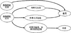
上电后,首先将本单元置为不在位、工作状态异常、备用,并且关闭倒换功能;After power-on, first set the unit as not in position, abnormal working state, standby, and turn off the switching function;
判断本单元是否插好、进行自检,自检通过后向管理软件申请注册;Judging whether the unit is plugged in, performing self-inspection, and applying for registration to the management software after the self-inspection passes;
管理软件根据槽位延时不同的时间打开主备倒换功能,允许本单元升主用,倒换设计仍然采用主降备,这里通过槽位延时控制可以保证一个单元先升主,另一个就是备用。The management software enables the master-standby switchover function according to the slot delay time, allowing the unit to be upgraded to the master, and the switchover design still adopts the master-standby mode. Here, the slot delay control can ensure that one unit is promoted to the master first, and the other is the standby .
在运行过程中,如果本单元插拔、不在位、状态不正常,都会影响主备关系发生变换。During operation, if the unit is plugged or unplugged, not in place, or in an abnormal state, it will affect the change of the master-standby relationship.
本发明实施例的主备倒换方法倒换逻辑设计分为主备指示信号在正常状态和在异常状态两种情况。The switching logic design of the master-standby switchover method in the embodiment of the present invention is divided into two cases: the master-standby indication signal is in a normal state and in an abnormal state.
请一并参阅表3和图6,主备倒换方法倒换逻辑设计在主备指示信号在正常状态流程包括:Please also refer to Table 3 and Figure 6. The switching logic design of the master-standby switchover method includes:
倒换使能关闭,倒换使能信号无效,本单元备用;The switching enable is turned off, the switching enabling signal is invalid, and this unit is for standby;
倒换使能打开分为三种情况:对单元主用,则本单元备用;本单元不在位,本单元备用;对单元备用,本单元在位、状态正常,本单元主用。There are three situations for enabling switching: the unit is in active use, and the unit is standby; the unit is not in place, and the unit is in standby; the unit is in standby, and the unit is in position and the status is normal, and the unit is in active use.
表3倒换真值表-正常状态Table 3 Switching Truth Table - Normal State
请一并参阅表4和图7;主备倒换方法倒换逻辑设计在主备指示信号在正常状态流程综合分析主备指示信号、状态信号、在位信号各种错误状态搭配,不考虑并发故障发生情况下包括:Please refer to Table 4 and Figure 7 together; the switchover logic design of the master-standby switchover method is to comprehensively analyze the combination of the master-standby indicator signals, status signals, and in-position signals in various error states in the process of the master-standby indicator signals in the normal state, regardless of concurrent failures. Situations include:
倒换使能打开,本单元在位,对单元主备指示信号为“11/00”情况下:本单元状态异常,本单元降备;“对单元在位、本单元WORK状态、对单元WORK状态”三个状态中大于1个状态出现异常,或者都正常,那么本单元主备关系保持;对单元状态异常或对单元不在位了,那么本单元升主。Switching is enabled, the unit is in position, and the master/standby indicator signal of the pair unit is "11/00": the state of the unit is abnormal, and the unit is downgraded to standby; "If more than one of the three states is abnormal, or all of them are normal, then the master-backup relationship of this unit remains; if the state of the unit is abnormal or the unit is not in place, then the unit is promoted to master.
对单元主备指示信号为“01”情况下:本单元状态异常,降备;本单元或对单元都状态异常情况下,对单元在位或不在位,本单元主备状态保持;对单元不在位,或对单元状态异常,本单元状态正常,本单元升主。When the active/standby indication signal of the paired unit is "01": the state of the unit is abnormal, and the standby is performed; when the state of the unit or the paired unit is abnormal, the active/standby state of the paired unit is maintained; the paired unit is not in position bit, or the status of the unit is abnormal, the status of the unit is normal, and the unit is promoted to master.
表4倒换逻辑-异常状态Table 4 Switching Logic - Abnormal State

本发明实施例的主备倒换方法综合考虑了所有接口信号的状态进行判断,给出合理的倒换处理措施,容错设计避免异常情况下硬件误倒换操作,提供可靠性的硬件倒换平台,并对出现的异常状态提供相应寄存器,软件定时查询这些状态寄存器,判断异常会上报告警,用户会及时得到故障提示,使新硬件倒换设计更加可靠。The active-standby switching method of the embodiment of the present invention comprehensively considers the status of all interface signals to judge, and provides reasonable switching processing measures. The fault-tolerant design avoids hardware switching operations under abnormal conditions, provides a reliable hardware switching platform, and responds to occurrences. The corresponding registers are provided for the abnormal state, and the software regularly checks these state registers, and reports an alarm when the abnormality is judged, and the user will get the fault prompt in time, making the new hardware switching design more reliable.
以上所述仅为本发明的较佳实施例而已,并不用以限制本发明,凡在本发明的精神和原则之内所作的任何修改、等同替换和改进等,均应包含在本发明的保护范围之内。The above descriptions are only preferred embodiments of the present invention, and are not intended to limit the present invention. Any modifications, equivalent replacements and improvements made within the spirit and principles of the present invention should be included in the protection of the present invention. within range.
Claims (6)
Priority Applications (1)
| Application Number | Priority Date | Filing Date | Title |
|---|---|---|---|
| CN2007100760014ACN101166415B (en) | 2007-07-09 | 2007-07-09 | Master/slave switch circuit and method |
Applications Claiming Priority (1)
| Application Number | Priority Date | Filing Date | Title |
|---|---|---|---|
| CN2007100760014ACN101166415B (en) | 2007-07-09 | 2007-07-09 | Master/slave switch circuit and method |
Publications (2)
| Publication Number | Publication Date |
|---|---|
| CN101166415A CN101166415A (en) | 2008-04-23 |
| CN101166415Btrue CN101166415B (en) | 2011-09-14 |
Family
ID=39334801
Family Applications (1)
| Application Number | Title | Priority Date | Filing Date |
|---|---|---|---|
| CN2007100760014AExpired - Fee RelatedCN101166415B (en) | 2007-07-09 | 2007-07-09 | Master/slave switch circuit and method |
Country Status (1)
| Country | Link |
|---|---|
| CN (1) | CN101166415B (en) |
Families Citing this family (3)
| Publication number | Priority date | Publication date | Assignee | Title |
|---|---|---|---|---|
| CN105281939A (en)* | 2014-07-17 | 2016-01-27 | 中兴通讯股份有限公司 | Method and device for reporting RXLOS (Receive Loss of Signal Alarm) |
| CN105471645B (en)* | 2015-12-01 | 2019-01-15 | 清华大学 | A kind of active and standby two-shipper common user communication interface and method |
| CN115733811B (en)* | 2021-08-27 | 2025-09-26 | 烽火通信科技股份有限公司 | Active/standby high-speed signal circuit switching method, device, equipment, and storage medium |
Citations (2)
| Publication number | Priority date | Publication date | Assignee | Title |
|---|---|---|---|---|
| CN1245999A (en)* | 1998-08-25 | 2000-03-01 | 深圳市华为技术有限公司 | Master backup reverse device |
| CN1412957A (en)* | 2002-05-22 | 2003-04-23 | 华为技术有限公司 | Method for providing clock in network equipment and its equipment |
- 2007
- 2007-07-09CNCN2007100760014Apatent/CN101166415B/ennot_activeExpired - Fee Related
Patent Citations (2)
| Publication number | Priority date | Publication date | Assignee | Title |
|---|---|---|---|---|
| CN1245999A (en)* | 1998-08-25 | 2000-03-01 | 深圳市华为技术有限公司 | Master backup reverse device |
| CN1412957A (en)* | 2002-05-22 | 2003-04-23 | 华为技术有限公司 | Method for providing clock in network equipment and its equipment |
Also Published As
| Publication number | Publication date |
|---|---|
| CN101166415A (en) | 2008-04-23 |
Similar Documents
| Publication | Publication Date | Title |
|---|---|---|
| US10108578B2 (en) | Single wire communications interface and protocol | |
| US9934187B2 (en) | Hot-pluggable computing system | |
| CN101378267B (en) | Primary and secondary switching device, and switching method using the same | |
| US20180101453A1 (en) | Implementing cable failover in multiple cable pci express io interconnections | |
| CN102622279B (en) | Redundancy control system, method and Management Controller | |
| US7558902B2 (en) | Bus to MCU bridge | |
| US20130115819A1 (en) | Adapter card for pci express x1 to compact pci express x1 | |
| CN104267713B (en) | Fault detection and switching method of ATO equipment of two-machine hot standby structure | |
| CN104917700A (en) | Management unit and exchange unit dual-redundancy switch | |
| CN104867437B (en) | ESD protection device for MIPI modules | |
| CN101166415B (en) | Master/slave switch circuit and method | |
| US6795933B2 (en) | Network interface with fail-over mechanism | |
| CN101131570B (en) | Redundancy switch-over control method and control circuit thereof | |
| CN102063356B (en) | A CPU heartbeat detection system and method for multiple central processing units | |
| CN201130309Y (en) | Redundant switching control circuit | |
| CN115408240A (en) | Redundant system active/standby method, device, equipment and storage medium | |
| WO2022057372A1 (en) | Iic hang link restoration circuit and method based on pca9511 chip | |
| US9959235B2 (en) | Input/output switching method, electronic device, and system for a server | |
| CN118316837A (en) | Test method for high-speed serial communication interconnection standard link state and plug-in card module | |
| CN107783862B (en) | An 8-way server master-slave BMC reset control method based on PCA9555 | |
| CN201196776Y (en) | Single plate and system with clock backup | |
| CN115408239A (en) | Redundancy system based on bus arbitration | |
| CN110825666B (en) | Fault switching method and system based on ARINC659 protocol | |
| CN220085382U (en) | Artificial Intelligence Acceleration Cards and Servers | |
| CN100409590C (en) | Devices for High System Availability |
Legal Events
| Date | Code | Title | Description |
|---|---|---|---|
| C06 | Publication | ||
| PB01 | Publication | ||
| C10 | Entry into substantive examination | ||
| SE01 | Entry into force of request for substantive examination | ||
| C14 | Grant of patent or utility model | ||
| GR01 | Patent grant | ||
| CF01 | Termination of patent right due to non-payment of annual fee | ||
| CF01 | Termination of patent right due to non-payment of annual fee | Granted publication date:20110914 |