CN101164048B - Security system implemented in the memory card - Google Patents
Security system implemented in the memory cardDownload PDFInfo
- Publication number
- CN101164048B CN101164048BCN2006800042296ACN200680004229ACN101164048BCN 101164048 BCN101164048 BCN 101164048BCN 2006800042296 ACN2006800042296 ACN 2006800042296ACN 200680004229 ACN200680004229 ACN 200680004229ACN 101164048 BCN101164048 BCN 101164048B
- Authority
- CN
- China
- Prior art keywords
- card
- test
- state
- operating state
- testing
- Prior art date
- Legal status (The legal status is an assumption and is not a legal conclusion. Google has not performed a legal analysis and makes no representation as to the accuracy of the status listed.)
- Expired - Fee Related
Links
Images


Classifications
- G—PHYSICS
- G06—COMPUTING OR CALCULATING; COUNTING
- G06K—GRAPHICAL DATA READING; PRESENTATION OF DATA; RECORD CARRIERS; HANDLING RECORD CARRIERS
- G06K19/00—Record carriers for use with machines and with at least a part designed to carry digital markings
- G06K19/06—Record carriers for use with machines and with at least a part designed to carry digital markings characterised by the kind of the digital marking, e.g. shape, nature, code
- G06K19/067—Record carriers with conductive marks, printed circuits or semiconductor circuit elements, e.g. credit or identity cards also with resonating or responding marks without active components
- G06K19/07—Record carriers with conductive marks, printed circuits or semiconductor circuit elements, e.g. credit or identity cards also with resonating or responding marks without active components with integrated circuit chips
- G—PHYSICS
- G06—COMPUTING OR CALCULATING; COUNTING
- G06F—ELECTRIC DIGITAL DATA PROCESSING
- G06F11/00—Error detection; Error correction; Monitoring
- G06F11/22—Detection or location of defective computer hardware by testing during standby operation or during idle time, e.g. start-up testing
- G06F11/2273—Test methods
- G—PHYSICS
- G06—COMPUTING OR CALCULATING; COUNTING
- G06F—ELECTRIC DIGITAL DATA PROCESSING
- G06F1/00—Details not covered by groups G06F3/00 - G06F13/00 and G06F21/00
- G—PHYSICS
- G06—COMPUTING OR CALCULATING; COUNTING
- G06F—ELECTRIC DIGITAL DATA PROCESSING
- G06F12/00—Accessing, addressing or allocating within memory systems or architectures
- G06F12/14—Protection against unauthorised use of memory or access to memory
Landscapes
- Engineering & Computer Science (AREA)
- Theoretical Computer Science (AREA)
- General Engineering & Computer Science (AREA)
- Physics & Mathematics (AREA)
- General Physics & Mathematics (AREA)
- Computer Hardware Design (AREA)
- Quality & Reliability (AREA)
- Computer Security & Cryptography (AREA)
- Microelectronics & Electronic Packaging (AREA)
- Storage Device Security (AREA)
- Credit Cards Or The Like (AREA)
Abstract
Description
Translated fromChinese技术领域technical field
本发明大体上涉及存储卡和加密,且具体地说,涉及通过卡中的测试机制消除对安全数据和密钥的存取。The present invention relates generally to memory cards and encryption, and in particular to eliminating access to secure data and keys through testing mechanisms in the card.
背景技术Background technique
在相当长时间以前,开发了一种通常称为智能卡的智能存储卡,且所述智能存储卡作为识别和支付形式在市场上获得公认。智能卡含有较小存储量以用于存储用户识别数据和用于存储交易相关数据。智能卡还经常被称为芯片卡,且在日本用于各种事物(例如国民身份证)并在许多地方用作一种类型的信用卡或借记卡。为了防止身份偷窃和其它金钱诈骗,已在所述卡和利用所述卡的系统中采用各种芯片设计和加密方案。Some time ago, a type of smart memory card, commonly referred to as a smart card, was developed and accepted in the market as a form of identification and payment. Smart cards contain a small amount of memory for storing user identification data and for storing transaction related data. Smart cards are also often referred to as chip cards and are used in Japan for various things such as national identification cards and in many places as a type of credit or debit card. To prevent identity theft and other monetary fraud, various chip designs and encryption schemes have been employed in the cards and systems utilizing them.
在设计和制造任何类型的安全存储卡中,存在两个竞争性关注问题。一个关注问题是使卡的安全性最大化,而另一个关注问题是使卡的可靠性最大化。为了使卡的可靠性最大化,重要的是能够在卡从工厂装运之前的各个制造阶段且在某些情况下甚至在卡已离开工厂之后测试卡的软件和硬件,以便执行故障分析。测试可包含通过芯片上的测试或接触垫的信号输入和输出,以测试卡的硬件和软件两者。这些测试例行程序和测试垫是确保质量控制所必需的,但也是对卡的安全数据、算法和密钥的潜在弱点或“后门”。因此,在使可靠性最大化与使安全性最大化(所必需的测试)之间总是存在一定程度的折衷。已经提出不同的方法来在测试完成之后关闭此“后门”。然而出于各种原因,迄今现有解决方案每一者均具有商业和技术缺陷。In designing and manufacturing any type of secure memory card, there are two competing concerns. One concern is to maximize card security, while another concern is to maximize card reliability. In order to maximize the reliability of a card, it is important to be able to test the card's software and hardware at various stages of manufacture before the card is shipped from the factory, and in some cases even after the card has left the factory, in order to perform failure analysis. Testing may involve signal input and output through test or contact pads on the chip to test both the hardware and software of the card. These test routines and test pads are necessary to ensure quality control, but are also potential weaknesses or "back doors" to the card's security data, algorithms and keys. Therefore, there is always some degree of trade-off between maximizing reliability and maximizing safety (required testing). Different methods have been proposed to close this "back door" after testing is complete. However, for various reasons, the existing solutions to date each have commercial and technical drawbacks.
在据信用于产生前述智能卡的一种方法中,在将存储器小片从晶片中切割出来之前测试卡的小片。将用于特定小片的测试垫定位在晶片的邻近小片上,且所述切割过程在测试之后将测试垫与邻近小片的所有电路切断。因此,存在于切割小片上的任何测试垫均作为对最终存储卡的安全数据的潜在后门而被完全隔离且关闭。然而,完全移除测试垫并非总是实用的或理想的。举例来说,缺乏可用的测试垫阻止了一定量的随后基于硬件的存储器测试,这(例如)限制了故障分析的潜在方法。In one method believed to be used to produce the aforementioned smart cards, the card dies are tested before the memory dies are diced from the wafer. The test pads for a particular die are positioned on adjacent dies of the wafer, and the dicing process cuts the test pads from all circuits of the adjacent die after testing. Therefore, any test pads present on the cut die are completely isolated and closed as a potential back door to the secure data of the final memory card. However, it is not always practical or desirable to completely remove the test pad. For example, the lack of available test pads prevents a certain amount of subsequent hardware-based memory testing, which, for example, limits potential methods of failure analysis.
尽管此方法对于通常仅具有用以保持识别和交易数据所必需的较小存储量的智能卡来说可能是优选的,但这对于测试用于存储多个大文件(例如照片和音乐)的大容量存储存储卡中所采用的相对较大存储量和较复杂安全例行程序来说是不足够的。这些大容量存储存储卡的一些实例是紧凑型快闪卡、MMC卡和SD卡。数字内容的传播和相关联的版权问题提升了安全性的重要性,而同时卡的测试和可靠性仍极为重要。需要一种用于制造、测试和操作安全大容量存储存储卡的较全面且灵活的系统,且所述系统由下文将描述的本发明提供。While this approach may be preferred for smart cards that typically only have the small amount of storage necessary to hold identification and transaction data, it is useful for testing large capacities for storing multiple large files such as photos and music. The relatively large amount of memory and the more complex security routines employed in the storage memory card are insufficient. Some examples of these mass storage memory cards are Compact Flash cards, MMC cards and SD cards. The spread of digital content and associated copyright issues has increased the importance of security, while card testing and reliability remain paramount. There is a need for a more comprehensive and flexible system for manufacturing, testing and operating secure mass storage memory cards, and said system is provided by the present invention as will be described below.
另一个重要方面是成本。若干种不同技术(例如非易失性存储器、逻辑和易失性存储器)可制作在单个集成电路小片(芯片)上。然而,在一个小片中混合不同技术显著增加了生产成本。在成本是主要驱动力的竞争环境中,非常需要限制在一个小片上提供的不同技术的量。然而,使用多个小片可能意味着在最终产品中敏感信息必须从一个小片传递到另一个小片。如果没有采用恰当的预防措施,那么这是黑客可利用的另一个潜在弱点。Another important aspect is cost. Several different technologies (such as non-volatile memory, logic, and volatile memory) can be fabricated on a single integrated circuit die (chip). However, mixing different technologies in one tablet significantly increases production costs. In a competitive environment where cost is the main driver, it is highly desirable to limit the amount of different technologies that can be offered on a single die. However, using multiple chips may mean that sensitive information must be passed from one chip to another in the final product. This is another potential weakness that hackers can exploit if proper precautions are not taken.
具体地说,将非易失性存储器位与同一小片内的逻辑混合是昂贵的。智能卡在运行智能卡的逻辑的同一小片中采用非易失性存储器用于数据存储目的,这是一种使安全性最大化的方法。然而,现今得益于本发明的存储卡必须存储非常大的音乐、照片、电影和其它用户文件。因此,制造可存储大量信息(在2005年约为几千兆字节且一直在增加)的单个集成电路小片存储卡是成本非常高的,且必须开发一种采用多个小片的安全系统。具体地说,非常需要建立一种利用一个或一个以上离散(具有成本效益的)快闪存储器小片的安全系统(采用加密和解密),所述快闪存储器小片与控制器小片分离且可在组装之前和之后进行彻底测试,而且所述系统不会经由测试机制而受到攻击。Specifically, mixing non-volatile memory bits with logic within the same die is expensive. Smart cards use non-volatile memory for data storage purposes in the same die that runs the smart card's logic, which is a way to maximize security. However, today's memory cards that benefit from the present invention must store very large music, photo, movie and other user files. Therefore, manufacturing a single integrated circuit die memory card that can store a large amount of information (on the order of several gigabytes in 2005 and increasing) is very costly, and a security system employing multiple dies must be developed. Specifically, there is a strong need to create a security system (using encryption and decryption) that utilizes one or more discrete (cost-effective) flash memory dies that are separate from the controller die and can be assembled Thorough testing is done before and after, and the system is not compromised through the testing mechanism.
发明内容Contents of the invention
因为利用具有当今数字装置所需的控制器功能性和大量存储的单个芯片的缩放性成本过高且存在问题,所以已开发了一种替代系统。通过单芯片解决方案,可用使得难以存取测试机制、加密密钥和加密内容的独特芯片设计来实现安全性。然而,通过将内容从单独存储器芯片传递到发生加密的控制器芯片的多芯片设计,必须特别注意保护对加密密钥和对加密内容的存取。此外,在最终组合件中(优选地)仍具有测试垫以允许测试组合系统的系统中,必须特别注意软件和硬件中可充当用于对加密密钥和内容进行未授权存取的后门的任何机制。Because scalability using a single chip with the controller functionality and large amounts of storage required by today's digital devices is cost-prohibitive and problematic, an alternative system has been developed. With a single-chip solution, security is implemented with a unique chip design that makes access to test mechanisms, encryption keys, and encrypted content difficult. However, with multi-chip designs that pass content from individual memory chips to a controller chip where encryption occurs, special care must be taken to protect access to encryption keys and to encrypted content. Also, in systems where test pads are still (preferably) in the final assembly to allow testing of the combined system, special attention must be paid to any features in the software and hardware that could act as backdoors for unauthorized access to encryption keys and content mechanism.
本发明具有在卡的寿命期间进入并通过的许多寿命周期阶段。依据阶段而定,卡中的逻辑启用或禁用加密引擎,控制对硬件(在晶片切割和卡组装之前和之后)和软件测试机制的存取,且控制密钥产生。这些阶段不仅允许在制造之前和之后彻底测试卡的硬件和软件两者(不同于移除了测试垫的智能卡),而且使得当卡处于安全阶段(当卡装运给用户时其所处的操作阶段)时实际上不可能存取加密密钥且因此不可能存取加密内容。因此,本发明提供一种可较好地被测试但还抵抗对卡内受保护数据的未授权存取的存储卡。The present invention has many life cycle stages to enter and pass through during the life of the card. Depending on the stage, logic in the card enables or disables the encryption engine, controls access to hardware (before and after wafer dicing and card assembly) and software testing mechanisms, and controls key generation. These stages not only allow for thorough testing of both the hardware and software of the card before and after manufacture (unlike smart cards with the test pads removed), but also allow the ) it is practically impossible to access the encryption key and thus the encrypted content. Accordingly, the present invention provides a memory card that is better tested but also resistant to unauthorized access to protected data within the card.
此外,需要一种用于制造、测试和操作安全大容量存储存储卡的较全面且灵活的系统,且所述系统由下文将描述的本发明提供。Furthermore, there is a need for a more comprehensive and flexible system for manufacturing, testing and operating secure mass storage memory cards, and said system is provided by the present invention as will be described below.
本发明的额外方面、优点和特征包含在以下对本发明示范性实施例的描述中,所述描述应结合附图来进行,其中在所有附图中相同标号用于描述相同特征。本文引用的所有专利、专利申请案、文章和其它公开案出于所有目的而以全文引用的方式并入本文中。Additional aspects, advantages and features of the invention are included in the following description of exemplary embodiments of the invention, which description should be taken in conjunction with the accompanying drawings, wherein like reference numerals are used to describe like features throughout. All patents, patent applications, articles, and other publications cited herein are hereby incorporated by reference in their entirety for all purposes.
附图说明Description of drawings
图1A是根据本发明实施例的系统10的示意图。FIG. 1A is a schematic diagram of a
图1B是系统10的另一实施例的示意图。FIG. 1B is a schematic diagram of another embodiment of
图2A是说明本发明实施例中各个寿命周期阶段的流程图。Figure 2A is a flow diagram illustrating the various life cycle phases in an embodiment of the present invention.
图2B是各个寿命周期阶段的图表。Figure 2B is a graph of various life cycle stages.
图3是说明引导过程和寿命周期阶段的流程图。Figure 3 is a flowchart illustrating the bootstrap process and lifecycle phases.
具体实施方式Detailed ways
存储器系统结构memory system structure
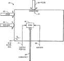
图1A的方框图说明可实施本发明各个方面的实例性存储器系统。如图1A所示,存储器系统10包含中央处理单元(CPU)或控制器12、缓冲管理单元(BMU)14、主机接口模块(HIM)16、快闪接口模块(FIM)18、快闪存储器20和外围存取模块22。存储器系统10通过主机接口总线26和端口26a与主机装置24进行通信。可为NAND类型的快闪存储器20为主机装置24提供数据存储。CPU 12的软件代码也可存储在快闪存储器20中。FIM 18通过快闪接口总线28连接到快闪存储器20,且在某些情况下如果快闪存储器20为可移除组件则通过端口(未图示)连接到快闪存储器20。HIM 16适合于连接到主机系统,如数码相机、个人计算机、个人数字助理(PDA)和MP-3播放器、手机或其它数字装置。外围存取模块22选择恰当的控制器模块(例如FIM、HIM和BMU)来与CPU 12进行通信。在一个实施例中,虚线框内系统10的所有组件可封闭在单个单元中,例如在存储卡中,且优选地封闭在卡中。The block diagram of Figure 1A illustrates an example memory system in which various aspects of the invention may be implemented. As shown in FIG. 1A, a
缓冲管理单元14包括主机直接存储器存取单元(HDMA)32、快闪直接存储器存取单元(FDMA)34、仲裁器36、CPU总线仲裁器35、寄存器33、缓冲随机存取存储器(BRAM)38和密码引擎40(也称为加密引擎40)。仲裁器36是共享的总线仲裁器,使得在任意时间仅一个主装置或发起装置(可为HDMA 32、FDMA 34或CPU 12)可为活动的,且从装置或目标装置为BRAM 38。仲裁器负责将恰当的发起装置请求通道传送到BRAM 38。HDMA 32和FDMA 34负责HIM 16、FIM 18与BRAM 38或RAM 11之间传送的数据。CPU总线仲裁器35允许从密码引擎40和快闪DMA 34经由系统总线15到RAM 11的数据传递,在某些情况下,例如当需要旁路密码引擎时使用所述系统总线15。HDMA 32和FDMA 34的操作是常规的,且本文无需详细描述。BRAM 38用于存储在主机装置24与快闪存储器20之间传递的数据。HDMA 32和FDMA 34负责在HIM 16/FIM18与BRAM 38或CPU RAM 12a之间传递数据和指示区段完成。The buffer management unit 14 includes a host direct memory access unit (HDMA) 32, a flash direct memory access unit (FDMA) 34, an
当主机装置24读取来自快闪存储器20的数据时,通过总线28、FIM 18、FDMA 34和密码引擎40获取存储器20中的加密数据,其中加密数据经解密并存储在BRAM 38中。接着将解密数据从BRAM 38通过HDMA 32、HIM 16、总线26发送到主机装置24。从BRAM 38获取的数据在传递到HDMA 32之前可借助于密码引擎40再次加密,使得发送到主机装置24的数据被再次加密,但与借以加密存储在存储器20中的数据的那些密钥和/或算法相比,是借助于不同的密钥和/或算法。或者,与在上述过程中将解密数据存储在BRAM 38中(所述数据可变得容易受到未授权存取)不同,来自存储器20的数据可被解密并在发送到BRAM 38之前由密码引擎40再次加密。接着如同以前那样将BRAM 38中的加密数据发送到主机装置24。此说明在读取过程期间的数据流。When
当主机装置24将数据写入到存储器20时,数据流的方向被反向。举例来说,如果主机装置通过总线26、HIM 16、HDMA 32将未加密数据发送到密码引擎40,那么此类数据可在存储在BRAM 38中之前由引擎40加密。或者,未加密数据可存储在BRAM 38中。数据接着在其去往存储器20的路径上在发送到FDMA 34之前被加密。When the
寿命周期阶段life cycle stage
当在存储卡(例如上文所述的存储卡)中实施时尤其有用的安全系统或安全操作系统(例如)具有不同的阶段或状态。优选地依次进入这些阶段,使得在从一个阶段进入到下一阶段之后,不能再次进入前一阶段。因此,可将其视为寿命周期阶段。A security system or a secure operating system that is particularly useful when implemented in a memory card such as the one described above, for example, has different phases or states. The stages are preferably entered sequentially such that after passing from one stage to the next, the previous stage cannot be re-entered. Therefore, it can be considered a life cycle phase.
在详细描述所述阶段之前,将简单论述另一系统级别图。图1B说明系统10的另一实施例。在此图式中为了简明和清楚起见,仅说明系统10的某些组件。存储器系统10包括测试垫(也称为硬件测试输入/输出(I/O))54。硬件总线(HW总线)56优选连接到测试垫54。这些测试垫和HW总线56连接到系统10的各个硬件和电路(未图示),且用于测试系统10的硬件和电路。JTAG总线62连接到系统总线15(见图1A),且可用于从系统10外部替换控制器固件和驱动器硬件块。其用于需要寄存器读取/写入操作的硬件测试。由于JTAG总线62可存取RAM和ROM,因此其也用于测试系统10的固件。主机总线26用于将诊断命令发送到系统10,且用于测试系统的固件。Before describing the phases in detail, another system level diagram will be briefly discussed. FIG. 1B illustrates another embodiment of
还展示了加密引擎40的NVM 50。存储在NVM 50内的是寿命周期状态77和秘密密钥99(的值)。NVM测试端口58用于测试加密引擎40内的NVM。The
状态指示器熔丝66用于指示产品处于NVM状态110(下文描述)而并非依赖于NVM内容。原因在于不能保证在制作期间存储在NVM中的初始值的可靠性。因此,使用另一较可靠的指示器,例如熔丝。如果熔丝被设定,那么系统将确定其处于状态110。如果系统10被复位,那么其将查看NVM寿命周期状态77以确定状态。
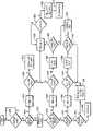
图2A说明各种状态和所述状态之间的转变次序。每一状态定义在卡被制造之前和之后卡(或其中实施所述卡的其它系统)的不同行为和能力,如以下表格中可见,所述表格还再现为图2B。Figure 2A illustrates various states and the sequence of transitions between the states. Each state defines different behaviors and capabilities of the card (or other system in which it is implemented) before and after the card is manufactured, as can be seen in the following table, also reproduced as Figure 2B.
状态优选地作为32位值存储在加密引擎的非易失性存储器内。在极大数目的可能(≈109)组合中存在可用于表示状态120-170的6个预先指派的值。所有其它值均指示状态110。这是因为不能保证在制作期间能够可靠地存储经定义的值并随后进行检索,因为制作、组装、测试和装运期间的各种处理操作可能改变存储器中的任何存储的值。The state is preferably stored as a 32-bit value in the encryption engine's non-volatile memory. There are 6 pre-assigned values that can be used to represent states 120-170 among an extremely large number of possible (≈109 ) combinations. All other values indicate
密钥值还优选地作为128位字段存储在加密引擎的非易失性存储器中。密钥值通常由播种算法随机产生。密钥的再生很可能改变密钥值,但这也不能保证,因为(伪)随机数产生器实际上可能连续产生相同的值。然而,即使人们充分了解密钥的值在再生期间可能不会改变,但在本申请案中改变密钥的术语可与再生密钥的术语互换使用。不用说,用于加密信息的密钥值是关键的。同一密钥值必须用于加密和解密两者。因此,如果在系统每次加电时再生密钥值,那么在所述加电之前加密的数据实际上是没有价值的,因为其不能用新密钥进行解密。尽管数据在实体上仍存在于卡的存储器中,但在没有正确的密钥值来对其进行解锁的情况下,所述数据是无用的。因此,如果黑客设法以某种方式迫使卡回到某一状态而并非回到安全状态150,那么他将不能够获得任何有价值的信息。在状态110和160中,在每次加电时将产生新密钥,且在状态150中用于先前存储信息的密钥将不能用于解密所述信息。在状态170和110中,无论密钥值如何,加密引擎均完全不可用。The key value is also preferably stored as a 128-bit field in the encryption engine's non-volatile memory. Key values are usually randomly generated by a seeding algorithm. Regeneration of the key is likely to change the key value, but this is not guaranteed either, since the (pseudo)random number generator may actually produce the same value continuously. However, even though one is well aware that the value of the key may not change during regeneration, the term change key is used interchangeably with the term regenerate key in this application. Needless to say, the key value used to encrypt information is critical. The same key value must be used for both encryption and decryption. Therefore, if the key value is regenerated every time the system is powered up, data encrypted prior to said power up is effectively worthless because it cannot be decrypted with the new key. Although the data still physically exists in the card's memory, it is useless without the correct key value to unlock it. Therefore, if a hacker somehow manages to force the card back to a state other than the
另一种安全性措施包括限制固件和硬件测试机制的可用性。系统包括将启用或禁用所述机制的逻辑。先前描述的主机总线是用于测试卡的固件的机制之一。主机可经由主机总线发出诊断命令以测试固件。当执行这些命令时也可测试硬件。还经由硬件总线以及提供对系统各个存储器的直接存取的JTAG端口来直接测试硬件。应注意,在状态140和150中,NVM测试机制、HW测试机制和FW测试机制全都被禁用。Another security measure includes limiting the availability of firmware and hardware testing mechanisms. The system includes logic that will enable or disable the mechanism. The previously described host bus is one of the mechanisms used to test the card's firmware. The host can issue diagnostic commands via the host bus to test the firmware. Hardware can also be tested while executing these commands. The hardware is also directly tested via the hardware bus as well as the JTAG port which provides direct access to the various memories of the system. It should be noted that in
现将进一步详细描述图2A中所见的状态和所述状态之间的通道。The states seen in Figure 2A and the pathways between the states will now be described in further detail.
状态110被称为控制器非易失性存储器(NVM)测试。此状态是存储器小片制作之后的初始状态,且是用于在将小片封装并安装到存储卡中之前测试控制器小片的非易失性存储器的状态。可在切割之前且同时小片整体仍为晶片形式时执行在此状态中进行的测试,或者可在切割之后在各个小片上执行所述测试。一旦测试了NVM,便将其内容(使用NVM测试器)进行初始化以指示状态120,且熔丝66熔断。在此状态中,加密引擎40被禁用。此状态仅设计为在卡的寿命周期中进入一次,且系统内没有用于返回到此状态的方法。然而,如先前论述,此状态由用于定义寿命周期状态的32位值的许多可能组合中除所述6个预先指派值以外的任何值来指示。如果检测到非法值且熔丝被熔断(不允许进入NVM状态110),那么密码引擎将永远不会就绪,且系统将不会进行引导或不会进行超过下文关于图3描述的步骤302。因此,每次卡被加电且处于此状态时,将随机产生新的密钥,且不可能解密先前加密的数据。即使密码引擎在此模式中没有被禁用,因为所述模式经设计为在制作期间晶片仍完整时使用,所以在每次加电时仍再生密钥,以防止可能以一些无法预见的方式进入此状态并尝试经由各种测试端口和机制来探查卡的安全数据的黑客。另外方面,故意地,在退出状态110之后,NVM测试机制不再可用。
状态120被称为恒定启用状态。在此状态中,密码引擎40被启用。密码引擎将使用的密钥不是由随机数产生器产生的,且不是存储在存储器中,而是硬连线到某个外部源且在此阶段期间恒定不变。硬件和软件测试机制在此状态中可用。通过硬件测试器进入此状态。
状态130被称为随机启用状态。此状态类似于状态120,然而,当进入状态130时,随机产生(一次)秘密密钥,而并非为恒定且硬连线的。这是用于存储卡的最终测试、特征化和资格化的状态。可使用秘密密钥或从所述秘密密钥导出的密钥用固件进行包含加密和解密的密码操作。通过由主机装置24载入系统10中并接着由系统10执行的代码进入此状态。
状态140被称为最终密钥状态。在此状态中,卡使用将随卡一起装运的最终秘密密钥。硬件和软件测试机制由卡逻辑禁用且不能被存取。此包含硬件测试总线和测试垫,见图1B。此状态用于向卡加载需要用随产品一起装运的密钥来保护的最终固件和配置数据。可在此状态中配置产品,而在状态150中不能进行配置。通过主机命令进入此状态。所述命令可包含在从主机下载并由卡执行的代码(“DLE代码”)中。或者可从主机直接发出命令。下文中使用术语DLE代码的任何时候都是这样的。
状态150被称为安全状态。这是卡从工厂装运时所处的状态。硬件和软件测试机制由卡逻辑禁用且不能被存取。在制造现场在产品的测试和配置结束时进入此状态。不再生密钥,且在状态150期间利用在状态140期间存储在存储器中的值。尽管对于卡的各种操作可利用导出的密钥,但密钥99对于导出那些密钥和加密与解密数据来说总是必要的。此密钥打算用于安全卡(在消费者手中作为安全卡时,而并非在此之后)的寿命。卡中的固件不能使用秘密密钥进行任何操作。加密引擎的硬件负责执行卡内的所有加密和解密。通过DLE代码进入此状态。
状态160被称为返回商品授权或RMA状态。此状态经设计为允许测试由于没有正确工作而被消费者返回的卡。这是可执行卡的故障分析的状态。软件和硬件测试机制再次可用。重要的是应注意此状态仅可由工厂访问。此外,在进入RMA状态之后,卡永远不能再次用作安全卡。换句话说,其永远不能再次进入状态150或以另外方式用于解密驻存在卡上的信息或将加密信息保存到卡上。当进入此模式且在卡处于此状态时执行的每次芯片复位期间再生秘密密钥。仅在引导时间启用使用秘密密钥进行解密的操作,且固件不能使用秘密密钥进行任何操作。通过作为主机命令的结果的ROM代码进入此状态。
状态170被称为禁用状态。在禁用状态中,密码引擎40处于旁路模式,其中所有密码能力被禁用。在卡内仅使用非安全算法。硬件和软件测试机制被再次启用,因为在没有加密引擎的情况下,没有任何事物值得攻击或以另外方式损害。任何加密信息可不再被解密且被视为无价值的。而且,可不对任何额外信息进行加密和随后解密。此状态可用于产生非安全或“常规”卡。以此方式,同一系统可用于生产安全和非安全存储卡两者。不同之处在于,在非安全卡中卡的安全系统处于禁用状态,或者所述卡可更一般地被称为处于状态170中。禁用状态也可用于再装运被发送回工厂进行故障分析且因此被传递到RMA状态160中的产品。如上提到,在卡进入RMA状态160中之后,其永远不能返回到任何先前状态,且永远不能再次作为安全卡出售。然而,可将具有功能或可在工厂再次被赋予功能的卡置于禁用状态170中,并作为非安全卡再次出售。以此方式,卡可被废物利用,且对于所有集中的目的将与新的非安全卡或“常规”卡相同。经废物利用的非安全卡和新的非安全卡将在相同状态中运行相同固件。
目前,绝大多数卡是非安全卡。尽管将安全卡带到市场的动力主要由于内容提供者的需要而较高,但对于安全卡对非安全卡,未来存储卡销售的百分比仍不清楚。清楚的是应该总是可能存在很多非安全内容且因此存在对非安全卡的需要。本发明不仅能够实现安全卡的所有硬件和软件的测试(仅由经授权的人员进行),而且提供将返回的安全卡进行废物利用以用于各种非安全用途的能力。此外,本发明的系统允许具有稳健安全性但无需被丢弃或使其安全系统折衷(具有可访问的“后门”)以便执行故障分析的卡。假定使用存储卡的装置广泛且日益激增,对原本将为有缺陷的安全卡的卡进行废物利用的能力对于消费者和制造商同样是个极大的益处。Currently, the vast majority of cards are non-secure cards. Although the drive to bring secure cards to the market is high mainly due to the needs of content providers, the percentage of future memory card sales remains unclear for secure versus non-secure cards. It should be clear that there should always be a lot of non-secure content and therefore a need for non-secure cards. The present invention not only enables testing of all hardware and software of the security card (only by authorized personnel), but also provides the ability to recycle returned security cards for various non-secure uses. Furthermore, the system of the present invention allows cards that have robust security but do not need to be discarded or have their security system compromised (with an accessible "back door") in order to perform failure analysis. Given the widespread and ever-proliferating number of devices using memory cards, the ability to recycle cards that would otherwise be defective security cards is of great benefit to consumers and manufacturers alike.
图3说明实施上述系统的存储卡的引导过程。关于引导过程的更多信息请参考颁予Micky Holtzman等人的第11/284,623号(代理人案号为SNDK.408US1)共同待决申请案“Method of Hardware Driver Integrity Check Of Memory Card Controller Firmware”,所述申请案以全文引用的方式并入本文中。Figure 3 illustrates the boot process of a memory card implementing the system described above. For more information on the boot process, refer to co-pending Application No. 11/284,623 (Attorney Docket No. SNDK.408US1) to Micky Holtzman et al., "Method of Hardware Driver Integrity Check Of Memory Card Controller Firmware," Said application is hereby incorporated by reference in its entirety.
在步骤302中,系统检查包含密码引擎40和其它组件在内的密码硬件是否就绪。在硬件就绪之前,系统将等待进行。当硬件就绪时,系统前进到步骤304。在步骤304中,系统检查以查看卡是否处于状态170(禁用状态)。如果卡处于状态170,那么在步骤306中系统将把作为最少量启动代码的引导载入程序(“BLR”)从快闪存储器20上载到RAM11。接着,在步骤308中系统检查以查看是否正确上载BLR。如果是,那么在步骤310中系统将上载在非安全模式中运行所必需的固件(标准固件减去密码功能性)。如果在步骤308中确定没有正确上载BLR,那么系统将前进到下文描述的步骤324。In
如果在步骤304中系统确定卡不处于状态170,那么在步骤312中系统将清除RAM内容。在此之后,系统将在步骤314中再次检查以查看卡处于何种状态。如果卡处于状态120、130或140,那么在步骤316中将上载BLR。在步骤318中,系统将检查以查看是否正确上载了BLR。接下来,在步骤320中,将执行BLR代码的完整性检查。此完整性检查是通过计算消息鉴别代码(MAC)值并将其与参考值进行比较而执行的基于硬件的检查。完整性检查的结果是存储在存储器中的简单旗标。在步骤322中,固件检查所述旗标以查看是否已验证了完整性。如果完整性没有问题,那么系统接着将在步骤342中上载在安全模式中运行所必需的固件,其当然也允许存储和检索非安全数据。如果在步骤322中确定完整性有问题,那么系统将等待来自主机的诊断命令以下载并执行来自主机的某些指令(DLE命令),如由步骤324表示。如果接收到DLE命令(如步骤326中所见),那么系统将在步骤328中着手将DLE代码载入到RAM中。在步骤330中,将由控制器执行DLE代码。If in
如果在步骤314中确定卡不处于状态120、130或140,那么系统在步骤332中将检查以查看卡是否处于状态150。如果是,那么系统接着将在步骤334中上载BLR。这是通过ROM代码完成的。如果BLR上载成功(如步骤336中所确定),那么在步骤338中将执行如上文在步骤320中描述的基于硬件的完整性检查。在此基于硬件的完整性检查之后,在步骤340中将执行另一完整性检查,此时为基于软件的完整性检查。如果完整性没有问题,那么系统接着将在步骤342中上载在安全模式中运行所必需的固件,其当然也允许存储和检索非安全数据。If it is determined in
如果在步骤332中确定卡不处于状态150,那么系统接着将检查卡的状态和卡是否处于状态160,且如果是,那么系统将等待如步骤348所表示的诊断命令。然而,如果在步骤344中确定卡不处于状态160,那么系统将等待命令以进入RMA状态160,如步骤346中所见。If it is determined in
Claims (12)
Translated fromChineseApplications Claiming Priority (7)
| Application Number | Priority Date | Filing Date | Title |
|---|---|---|---|
| US65112805P | 2005-02-07 | 2005-02-07 | |
| US60/651,128 | 2005-02-07 | ||
| US11/317,390US8108691B2 (en) | 2005-02-07 | 2005-12-22 | Methods used in a secure memory card with life cycle phases |
| US11/317,862 | 2005-12-22 | ||
| US11/317,390 | 2005-12-22 | ||
| US11/317,862US8321686B2 (en) | 2005-02-07 | 2005-12-22 | Secure memory card with life cycle phases |
| PCT/US2006/003876WO2006086232A2 (en) | 2005-02-07 | 2006-02-01 | Secure memory card with life cycle phases |
Publications (2)
| Publication Number | Publication Date |
|---|---|
| CN101164048A CN101164048A (en) | 2008-04-16 |
| CN101164048Btrue CN101164048B (en) | 2010-06-16 |
Family
ID=36644859
Family Applications (1)
| Application Number | Title | Priority Date | Filing Date |
|---|---|---|---|
| CN2006800042296AExpired - Fee RelatedCN101164048B (en) | 2005-02-07 | 2006-02-01 | Security system implemented in the memory card |
Country Status (7)
| Country | Link |
|---|---|
| EP (1) | EP1846826A2 (en) |
| JP (1) | JP4787273B2 (en) |
| KR (1) | KR100972540B1 (en) |
| CN (1) | CN101164048B (en) |
| IL (1) | IL184793A0 (en) |
| TW (1) | TWI402755B (en) |
| WO (1) | WO2006086232A2 (en) |
Families Citing this family (9)
| Publication number | Priority date | Publication date | Assignee | Title |
|---|---|---|---|---|
| US7748031B2 (en) | 2005-07-08 | 2010-06-29 | Sandisk Corporation | Mass storage device with automated credentials loading |
| US8966284B2 (en) | 2005-09-14 | 2015-02-24 | Sandisk Technologies Inc. | Hardware driver integrity check of memory card controller firmware |
| US8915447B2 (en) | 2007-09-12 | 2014-12-23 | Devicefidelity, Inc. | Amplifying radio frequency signals |
| US8070057B2 (en) | 2007-09-12 | 2011-12-06 | Devicefidelity, Inc. | Switching between internal and external antennas |
| US9304555B2 (en) | 2007-09-12 | 2016-04-05 | Devicefidelity, Inc. | Magnetically coupling radio frequency antennas |
| US8109444B2 (en) | 2007-09-12 | 2012-02-07 | Devicefidelity, Inc. | Selectively switching antennas of transaction cards |
| US9311766B2 (en) | 2007-09-12 | 2016-04-12 | Devicefidelity, Inc. | Wireless communicating radio frequency signals |
| US9553721B2 (en)* | 2015-01-30 | 2017-01-24 | Qualcomm Incorporated | Secure execution environment communication |
| CN116230065A (en)* | 2023-02-14 | 2023-06-06 | 北京国家新能源汽车技术创新中心有限公司 | Method for testing erasing life of embedded nonvolatile memory of security chip, storage medium and computer |
Citations (1)
| Publication number | Priority date | Publication date | Assignee | Title |
|---|---|---|---|---|
| US6783078B1 (en)* | 2003-05-09 | 2004-08-31 | Stmicroelectronics, Inc. | Universal serial bus (USB) smart card having read back testing features and related system, integrated circuit, and methods |
Family Cites Families (16)
| Publication number | Priority date | Publication date | Assignee | Title |
|---|---|---|---|---|
| DE4243888A1 (en)* | 1992-12-23 | 1994-06-30 | Gao Ges Automation Org | Data carrier and method for checking the authenticity of a data carrier |
| FR2716989B1 (en) | 1994-03-04 | 1996-04-05 | Gemplus Card Int | Method of operation of a smart card. |
| JP3461234B2 (en)* | 1996-01-22 | 2003-10-27 | 株式会社東芝 | Data protection circuit |
| EP1004992A3 (en)* | 1997-03-24 | 2001-12-05 | Visa International Service Association | A system and method for a multi-application smart card which can facilitate a post-issuance download of an application onto the smart card |
| JPH11161549A (en)* | 1997-11-28 | 1999-06-18 | Toshiba Corp | Secret information management method and system for portable information equipment |
| AU3841999A (en)* | 1998-06-05 | 1999-12-30 | Landis & Gyr Communications Sarl | Preloaded ic-card and method for authenticating the same |
| EP0992809A1 (en)* | 1998-09-28 | 2000-04-12 | Siemens Aktiengesellschaft | Circuit with deactivatable scan path |
| JP2000172821A (en)* | 1998-12-10 | 2000-06-23 | Toshiba Corp | Semiconductor device, data storage medium, data recording device, data reading device, and method of manufacturing semiconductor device |
| US7023996B2 (en)* | 2001-05-04 | 2006-04-04 | The Boeing Company | Encryption for asymmetric data links |
| DE10162306A1 (en)* | 2001-12-19 | 2003-07-03 | Philips Intellectual Property | Method and arrangement for verifying NV fuses as well as a corresponding computer program product and a corresponding computer-readable storage medium |
| JP4350962B2 (en)* | 2002-03-13 | 2009-10-28 | パナソニック株式会社 | Secure device |
| US6912633B2 (en)* | 2002-03-18 | 2005-06-28 | Sun Microsystems, Inc. | Enhanced memory management for portable devices |
| US6843423B2 (en)* | 2003-03-13 | 2005-01-18 | Stmicroelectronics, Inc. | Smart card that can be configured for debugging and software development using secondary communication port |
| TW200501281A (en)* | 2003-06-27 | 2005-01-01 | Kingpak Tech Inc | Manufacturing method of small memory card having display |
| EP1649410A2 (en)* | 2003-07-17 | 2006-04-26 | SanDisk Corporation | Memory card with raised portion |
| TWI223974B (en)* | 2003-11-20 | 2004-11-11 | Advanced Semiconductor Eng | Tiny memory card and method for manufacturing the same |
- 2006
- 2006-02-01EPEP06734304Apatent/EP1846826A2/ennot_activeWithdrawn
- 2006-02-01JPJP2007554249Apatent/JP4787273B2/ennot_activeExpired - Fee Related
- 2006-02-01CNCN2006800042296Apatent/CN101164048B/ennot_activeExpired - Fee Related
- 2006-02-01WOPCT/US2006/003876patent/WO2006086232A2/enactiveApplication Filing
- 2006-02-01KRKR1020077018143Apatent/KR100972540B1/ennot_activeExpired - Fee Related
- 2006-02-07TWTW095104117Apatent/TWI402755B/ennot_activeIP Right Cessation
- 2007
- 2007-07-23ILIL184793Apatent/IL184793A0/ennot_activeIP Right Cessation
Patent Citations (1)
| Publication number | Priority date | Publication date | Assignee | Title |
|---|---|---|---|---|
| US6783078B1 (en)* | 2003-05-09 | 2004-08-31 | Stmicroelectronics, Inc. | Universal serial bus (USB) smart card having read back testing features and related system, integrated circuit, and methods |
Also Published As
| Publication number | Publication date |
|---|---|
| JP2008530659A (en) | 2008-08-07 |
| JP4787273B2 (en) | 2011-10-05 |
| IL184793A0 (en) | 2008-01-20 |
| TW200641696A (en) | 2006-12-01 |
| KR20070121642A (en) | 2007-12-27 |
| WO2006086232A3 (en) | 2007-10-11 |
| KR100972540B1 (en) | 2010-07-28 |
| EP1846826A2 (en) | 2007-10-24 |
| WO2006086232A2 (en) | 2006-08-17 |
| TWI402755B (en) | 2013-07-21 |
| CN101164048A (en) | 2008-04-16 |
Similar Documents
| Publication | Publication Date | Title |
|---|---|---|
| US8423788B2 (en) | Secure memory card with life cycle phases | |
| CN101164048B (en) | Security system implemented in the memory card | |
| US8108691B2 (en) | Methods used in a secure memory card with life cycle phases | |
| US8321686B2 (en) | Secure memory card with life cycle phases | |
| US8572410B1 (en) | Virtualized protected storage | |
| CN115019874B (en) | Secure device status apparatus and method | |
| US11222144B2 (en) | Self-encrypting storage device and protection method | |
| CN101263501B (en) | Hard Drive Integrity Check for Memory Card Controller Firmware | |
| US20190163913A1 (en) | Root key processing method and associated device | |
| US20080107275A1 (en) | Method and system for encryption of information stored in an external nonvolatile memory | |
| US20070297606A1 (en) | Multiple key security and method for electronic devices | |
| EP1638033A2 (en) | Self testing and securing RAM system and method | |
| US20070237325A1 (en) | Method and apparatus to improve security of cryptographic systems | |
| US8266449B2 (en) | Security for storage devices | |
| TW200832427A (en) | Virtual secure on-chip one time programming | |
| TWI541825B (en) | Non-volatile memory to store resettable data | |
| US9152576B2 (en) | Mode-based secure microcontroller | |
| US8190920B2 (en) | Security features in an electronic device | |
| US11481523B2 (en) | Secure element | |
| WO2008071222A1 (en) | Protecting a programmable memory against unauthorized modification | |
| CN109583196B (en) | Key generation method | |
| CN109598150B (en) | Key using method | |
| CN104794373A (en) | Software encryption lock | |
| RU2007148810A (en) | METHOD FOR TRUSTED DOWNLOAD OF OPERATING SYSTEM OF SOFTWARE AND HARDWARE COMPLEX |
Legal Events
| Date | Code | Title | Description |
|---|---|---|---|
| C06 | Publication | ||
| PB01 | Publication | ||
| C10 | Entry into substantive examination | ||
| SE01 | Entry into force of request for substantive examination | ||
| C14 | Grant of patent or utility model | ||
| GR01 | Patent grant | ||
| ASS | Succession or assignment of patent right | Owner name:SANDISK TECHNOLOGIES, INC. Free format text:FORMER OWNER: SANDISK CORP. Effective date:20150814 | |
| C41 | Transfer of patent application or patent right or utility model | ||
| TR01 | Transfer of patent right | Effective date of registration:20150814 Address after:American Texas Patentee after:Sandisk Corp. Patentee after:Discretix Technologies Ltd. Address before:American California Patentee before:Sandisk Corp. Patentee before:Discretix Technologies Ltd. | |
| CF01 | Termination of patent right due to non-payment of annual fee | ||
| CF01 | Termination of patent right due to non-payment of annual fee | Granted publication date:20100616 Termination date:20180201 |