Movatterモバイル変換


[0]ホーム

URL:


CN101164006A - Light redirecting films and film systems - Google Patents

Light redirecting films and film systems
Download PDF

Info

Publication number
CN101164006A
CN101164006ACNA2005800406480ACN200580040648ACN101164006ACN 101164006 ACN101164006 ACN 101164006ACN A2005800406480 ACNA2005800406480 ACN A2005800406480ACN 200580040648 ACN200580040648 ACN 200580040648ACN 101164006 ACN101164006 ACN 101164006A
Authority
CN
China
Prior art keywords
light
film
substrate
optical
optical modules
Prior art date
Legal status (The legal status is an assumption and is not a legal conclusion. Google has not performed a legal analysis and makes no representation as to the accuracy of the status listed.)
Granted
Application number
CNA2005800406480A
Other languages
Chinese (zh)
Other versions
CN100578291C (en
Inventor
杰弗瑞·R·派克
提摩西·A·麦考卡棱
Current Assignee (The listed assignees may be inaccurate. Google has not performed a legal analysis and makes no representation or warranty as to the accuracy of the list.)
Solid State Opto Ltd
Original Assignee
Solid State Opto Ltd
Priority date (The priority date is an assumption and is not a legal conclusion. Google has not performed a legal analysis and makes no representation as to the accuracy of the date listed.)
Filing date
Publication date
Application filed by Solid State Opto LtdfiledCriticalSolid State Opto Ltd
Publication of CN101164006ApublicationCriticalpatent/CN101164006A/en
Application grantedgrantedCritical
Publication of CN100578291CpublicationCriticalpatent/CN100578291C/en
Anticipated expirationlegal-statusCritical
Expired - Fee Relatedlegal-statusCriticalCurrent

Links

Images

Classifications

Landscapes

Abstract

The light redirecting films of the present invention have a pattern of individual optical elements that may intersect and/or interlock each other to achieve substantially complete surface coverage of at least one of the surfaces occupied by the optical elements. At least some of the optical elements may have at least one flat surface and at least one curved surface that may intersect each other to a greater extent on the curved surface than on the flat surface to increase the relative percentage of flat surface area to curved surface area of the intersecting optical elements to increase the on axis gain of light passing through the film.

Description

Light changed course film and membrane system
Technical field
The invention relates to light changed course film and membrane system, be used to alter course from the light of a light source and towards perpendicular to one of the plane of film direction.
Background technology
Light changed course film is transparent or semitransparent optical thin film or the substrate that approaches, and its redistribution is by the light of film, and the distribution that makes the light that withdraws from film is the surface of pointing to more perpendicular to film.So far, light changed course film is to be provided with prism-like groove, lensing groove or pyramid part to withdraw from (exit) surface at the light of film, the angle of the light of film at film/air interface withdrawed from its change, and causes component that the incident ray on one of the refractive surface of advancing perpendicular to groove plane distributes for being distributed in more one of surface perpendicular to film direction again.This light changed course film is to be applied to for example LCD, and it is applied to laptop computer, word processor, aviation display, mobile phone, PDA(Personal Digital Assistant) and similarly local, so that display is for brighter.
It is to have transparent or matt (matte) coating (finish) usually that the light of film enters (entrance) surface, decides on desired visual appearance.One matt coating is to produce comparatively soft image and bright, owing to tarnish or caused extra scattering of diffusing surface and the light loss that causes.
So far, most application is two thin layers with groove that use relative to each other rotation, so that be at 90 degree and relative to each other in the groove of each other thin layer.Being directed to this reason is to be: the light changed course film with groove is the component that only redistributes the incident ray distribution on one of the refractive surface of advancing perpendicular to groove plane, makes it towards the direction perpendicular to film surface.Therefore, light is the normal toward the film surface of two dimension in order to alter course, be relevant to that to revolve two thin layers with groove that turn 90 degrees each other be necessary, thin layer is that changed course is advanced perpendicular to the light on a plane of the direction of its groove, and another thin layer is that changed course is advanced perpendicular to the light on a plane of the direction of its groove.
Past has attempted to produce the light changed course film of simple layer, the component of its incident ray distribution of advancing along two disalignments that are 90 degree each other of will altering course.Reach one of this measure usual way and provide and have the film of extension, and cause a kind of pyramid structure of the light of advancing in these two directions of altering course perpendicular to the simple layer of each other two groups of grooves.Yet, this kind film is to produce more much lower brightness (compared to revolving two thin layers that each person who turn 90 degrees has single groove framework each other), because because second group groove of simple layer film has removed the zone of first group groove, essence reduces the surface area that can utilize with changed course light and reaches 50% at each direct of travel.
In addition, the groove of the film of light changed course so far is to constitute, and makes all grooves for be contacted with the surface of film in identical angle, mostly is 45 degree greatly.This design is that hypothesis is fixing from one of light of light source, the diffusion angular distribution, light source be such as: a lambert (lambertian) source, utilization one print or etching technique to take out one of the light backlight panel or a square backlight panel the severe fan diffuser after.All light changed course surfaces all are contacted with film with identical angle a kind of light changed course film is that optimization is not in a light source, and the latter has the non-homogeneous durection component of one of zones of different for above light source.For example, the backlight of one modern high-level efficiency edge light (utilization groove or micro-optical surface are to take out light) is in its average angle, be to change, and need be normal with the best changed course light in the different angles that light alters course between surface and the thin film planar towards film in the different distance place of this light source certainly.
Therefore, just have the needs for a kind of light changed course film, it can produce softer image and exempt a tarnish of the light input side that is associated with film or the brightness of diffusion coating reduces.In addition, just there are needs for the film of simple layer, the part of its light of advancing of can altering course in one of the refractive surface that is parallel to plough groove type film plane, this film is compared to the film of the simple layer of utilization prism or lens groove and brighter.In addition, have the needs that are directed to a kind of light changed course film, it can compensate and be directed to existence for a specific light source and the different angles of the light at the diverse location place above light source distribute, this light source such as: utilization with the illumination LCD backlight.In addition, have the needs that are directed to a kind of light changed course membrane system, wherein, this film is that coupling or the light output that is adjusted to a backlight or other light source distribute, with reset orientation or changed course from the more incident ray of backlight within the visual angle of an expectation.
Summary of the invention
The invention relates to light changed course film and light changed course membrane system, its the more light changed course that will be launched by a backlight or other light source is towards more perpendicular to the direction on the plane of film, and the present invention is about the light film that alters course, it produces comparatively soft image and onrelevant reduces having the brightness that light enters the film of the tarnish on surface or diffusion coating, and the effect of raising is arranged.
It is to have one of discrete indivedual optical modules of well defining shape pattern (pattern) that the light of film withdraws from the surface, is used to reflect the incident distribution of light, is more perpendicular to the direction on the surface of film so that withdraw from the distribution of light of film.These indivedual optical modules are that depressed part that withdraws from the surface or the teat owing to film forms, and comprise one or more inclined surface, are used to reflect incident ray for towards perpendicular to a direction that withdraws from the surface.For example, these inclined surfaces are to comprise the combination of one of smooth and curved surface, and its changed course light is within the visual angle of an expectation.In addition, the crooked area of the curvature on these surfaces or indivedual optical modules can change the ratio of smooth area and the peripheral shape system of crooked and flat surfaces, light output with special these films distributes, and uses the visual angle of the display device of these films with customization.In addition, the crooked area of the curvature that these are surperficial or indivedual optical modules is to change to the ratio of smooth area, with the advance light more or less on a plane of the groove that is parallel to prism or lens plough groove type film of changed course.In addition, the curvature on these surfaces of the size of indivedual optical modules and number of clusters and indivedual optical modules is to choose, to produce diffusion output more or less, or randomization is from the input distribution of light of light source, distribute with the light output that produces comparatively soft more diffusion, and keep output and be distributed within the specified angle zone perpendicular to the direction of film.
It is to have an optics coating (coating) that the light of film enters the surface, such as: an antireflective coating, a reflection polarizer, are delayed (retardation) coating, a polarization circulation coating or a polarizer.In addition, a tarnish or diffusion texture system can be arranged at light and enter the surface, decide on desired visual appearance.One lacklustre coating is to produce comparatively soft image, but it is not brighter.
Can serve as reasons single or a plurality of material or material layer of film constitutes, and can have all zone or all layers of different refractive indexes.In addition, particulate is to be added into these films, to produce the optical effect of an expectation.
But the indivedual optical modules that withdraw from the surface at these films are randomizations, so that exempt itself and any interference (interference) at the pixel (pixel) of LCD interval.This randomization is size, shape, position, the degree of depth, orientation, angle or the density that can comprise these optical modules.This is the demand of exempting for diffusion layer, to eliminate ripple (moir é) and similar effect.This randomization and/or curved surface is set is also to can be utilization to decompose the image of this backlight in indivedual optical modules.Moreover, at least some persons of indivedual optical modules be configurable be the surface of withdrawing from group (grouping) across film, and these optical modules of each group to have part at least be to have a different size or shape facilities, it is for each group that changes across film and collective produces an average size or a shape facility, obtaining surpassing the average eigenwert of the coupling tolerance deviation (tolerance) be directed to any single optical module, and eliminate ripple and interference effect about the pixel interval of a LCD.In addition, indivedual optical modules have at least part be can be relative to each other and the orientation in different angles, to customize these films reset orientation and changed course of light is the ability along two disalignments.
The light changed course surface of indivedual optical modules and the light of these films withdraw from the angle that the surface made and also can be changed to across the viewing area of a LCD, with the light changed course function of special these films being that one of inhomogeneous light output distributes at surface across light source.
Indivedual optical modules of light changed course film are also desirable for being overlapped in the configuration of one staggered (staggered), interlocking (interlocked) and/or crossing (intersecting) each other, have a kind of optical texture of superior surf zone covering with foundation.Moreover indivedual optical modules are configurable in group, indivedual optical modules part is arranged is the orientation for being that the orientation is along another axle along other indivedual optical modules.In addition, the orientation at indivedual optical modules of each group is to change.Moreover size, shape, position and/or the orientation of indivedual optical modules of light changed course film are to change, with the variation of the distribution of considering the light of being launched by a light source.
The character and the pattern of the optical module of light changed course film are also customizable, with at the light source of the different types that sends the different light rays distribution and these light changed course films of optimization, for example: single bulb laptop computer person with a kind of pattern, two bulb flat-panel monitor with another kind of pattern, or the like.
Moreover, light changed course membrane system is proposed, wherein, orientation, size, position and/or the shape of indivedual optical modules of light changed course film are special, distribute with the light output that is directed to a backlight or other light source, with reset orientation or changed course from more persons of the incident ray of this backlight within the visual angle of expectation.In addition, this backlight is to comprise that collimated ray is other optical skew (deformity) along, and light changed course film system can comprise that collimated ray is along the indivedual optical modules perpendicular to this another axle of.
In order to reach aforementioned and relevant purpose, the present invention comprises more complete being described in hereinafter and the specific characteristics of pointing out in claim, the following description with enclose graphic be the embodiment of some illustrative of set forth in detail the present invention, yet, these contents be the indication the present invention the exercisable various ways of theory in the minorities.
Description of drawings
The 1st figure is the diagrammatic side view of the light changed course membrane system of a kind of form according to the present invention;
The 2nd figure is the amplification fragment side view of a part of the backlight and light changed course membrane system of the 1st figure;
The 3rd and 4 figure are diagrammatic side view of light changed course membrane system of other form of the present invention;
The the 5th to 20 figure is schematic isometric or planimetric map, is shown in the different pattern of indivedual optical modules of the present invention's light changed course film;
5a to 5n figure is the schematic isometric of the different geometries that may take in indivedual optical modules of light changed course film;
The 21st figure is the schematic isometric of a kind of light changed course film, has the optics groove that extends in the face of one of film one corner bending pattern across film;
The 22nd figure is the plan view from above of a kind of light changed course film, has extension across film and in the face of a pattern of the optics groove of the mid point at one of film edge, it is along with the distance from this edge reduces curvature for increase;
The 23rd figure is the end-view of the light changed course film of the 22nd figure, as from its left end;
The 24th figure is the side view of the light changed course film of the 22nd figure;
The 25th and 26 figure be a kind of backlight/the amplification signal fragment planimetric map of one of luminescent panel assembly surf zone, show the optical skew of the various forms on a surface that is formed at backlight;
The 27th and 28 figure are respectively one amplification longitudinal cross-section by the optical skew of the 25th and 26 figure;
The 29th and 30 figure be by a surface that is formed at a backlight go up or among amplifications of optical skew of other form illustrate the longitudinal cross-section;
The the 31st to 39 figure is the amplification schematic isometric of backlight surf zone, contains all patterns that other well defines indivedual optical skews of shape;
The 40th figure be by a surface that is formed at a backlight go up or among amplifications of optical skew of another form illustrate the longitudinal cross-section;
The 41st and 42 figure are amplification diagrammatic top plan view of backlight surf zone, contain to be shaped as to be similar to the optical skew shown in the 37th and 38 figure, and it is the length in zone and width and be disposed at a plurality of arrays surfacewise;
The 43rd and 44 figure are amplification diagrammatic top plan view of backlight surf zone, contain shape also for being similar to the optical skew shown in the 37th and 38 figure, its surfacewise the zone length and be disposed at all row that stagger;
The 45th and 46 figure are amplification diagrammatic top plan view of backlight surf zone, contain in the at random a kind of or variable pattern of the optical skew of the different size of surf zone;
The 47th figure is the amplification schematic isometric of a backlight surf zone, shows the length in zone surfacewise, and along with the distance increase on optical skew and light input surface or the intensity of light reduces, the size of optical skew is increase;
The 48th and 49 figure are schematic isometric, show along the different angles orientation of the optical skew of the length of a backlight surf zone and width;
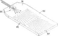
The 50th and 51 figure are amplification stereograms, and signal shows that how emission is reflected by the different indivedual optical skews that well define shape of a backlight surf zone or reflected from the light system of the example of a focused light source;
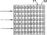
The 52nd and 54 figure be on the surface of one of a kind of optics changed course film optical transparent substrate or among the amplification plan view of two indivedual optical modules that well define shape, each optical module cording has one of common formation one spine a flat surfaces and a curved surface, and these optical modules systems intersect each other along the different piece of the curved surface of optical module;
The 53rd and 55 figure are the schematic isometric that are respectively the optical module of the 52nd and 54 figure;
The 56th figure is an amplification stereogram, signal show on the surface of one of a kind of optics changed course film optical transparent substrate or among indivedual optical modules, it has one of the side of two bendings or surface asymmetric shape;
The 57th figure is a schematic plan view, shows the optical module of two the 56th figure that intersect each other;
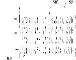
The 58th figure is the schematic isometric of the optical module of the 57th figure;
The 59th figure be on one of a kind of optics changed course film optical transparent substrate or among the amplifications signal fragment planimetric map of a part of one of the indivedual non-interlockable optical module that well defines shape pattern on surface, non-interlockable optical module system configuration makes so being covered as maximum of substrate surface of occupying and not intersecting each other;
The 60th and 61 figure be similar on the surface of one of a kind of optics changed course film optical transparent substrate of the 59th figure or among part person's amplifications of pattern of the indivedual non-interlockable optical module that well defines shape illustrate the fragment planimetric map, but it shows that non-interlockable optical module intersects each other in the difference amount, to increase the overlay capacity by the non-interlockable substrate surface that optical module was occupied;
The the 62nd to 64 figure is attached or is assembled to the amplification plan view of the non-interlockable optical module of different interlockable geometric configuratioies;
The amplification view of the derandominzation pattern of one of wedge shape optical module that the 65th figure right and wrong are interlockable form;
The amplification view of the randomized patterns of one of wedge shape optical module that the 66th figure right and wrong are interlockable form;
The 67th figure amplifies schematic isometric, be shown in that one of a kind of light changed course film surface is gone up or among one of optical module radial pattern;
The 68th figure is the amplification schematic isometric of indivedual optical modules that a kind of light changed course film on two surfaces is only arranged, and two surfaces are smooth or a plane surface and a curved surface, and it forms the spine of a uniqueness jointly;
The 69th figure has many amplifications schematic isometric of another indivedual optical modules of light changed course film, the spine of the how right a plurality of uniquenesses of the common formation of surface system to be planted in one of surface;
The 70th figure is the amplification schematic isometric that is similar to indivedual optical module shapes of the 68th figure those shown, except the optical module of the 70th figure ties up to these two surfaces circular spine of formation place with a non-uniqueness jointly;
The 71st figure also is the amplification schematic isometric that is similar to indivedual optical module shapes of the 69th figure those shown, except the optical module cording of the 71st figure has the spine and smooth, circular, the crooked or peak portion that distorts of a non-uniqueness, it reduces the peak portion degree of depth or the height of optical module;
The 72nd and 73 figure are respectively the further amplification schematic isometric of indivedual optical module shapes of the 70th and 71 figure, show the feature of all sizes of these optical modules;
The the 74th to 78 figure is the diagrammatic side view of light changed course membrane system of the present invention's other form; And
The 79th and 80 figure are schematic isometric of light changed course membrane system of the present invention's other form.
[primary clustering symbol description]
1: light changed course membrane system
2: light changed course film
5: optical module
6: light withdraws from the surface
7: light enters the surface
8: transparent membrane or substrate
10: flat surfaces
12: curved surface
13: taper shape
14: hemisphere or domed shape
15,16: curved surface
17: flat surfaces
18: Pyramid
19: leg-of-mutton side
20: smooth inclined lateral side
22: smooth side tilts
23: circle or bent back ends or side
24: circle or curved top portion
25: the optics coating
26: light source
30: optical diffusion layer
32: group
35: the optics groove
40: back reflector
41: volume
50: optical skew
51: teat
52: backlight surf zone (panel surface zone)
53: depressed part
54,59,64,67,73: reflectivity/refractivity surface
55: intersect the edge
56,68: the surrounding edge part
57,60,65,69,74: end wall
58,58 ', 63,66,71,72: light is drawn distortion
61,62,70,75: sidewall
76,77,78,80,85: distortion
79: flat surfaces
81: depressed part
82: troop
86,87: row
90: light
91: the light transitional region
92: the luminescent panel member
93: one of panel member side
94: the opposite side of panel member
95: the input edge of panel member
96: one of substrate surface
97: spine
98: paired optical module
99: all row that stagger
100: pattered region (area) not
101-103: base shape
105: the derandominzation pattern
106: randomized patterns
110: spine's section of non-uniqueness
112: circular spine's section
113: peak portion of spine
115: light changed course membrane system
116: light-emitting area
117: light enters the surface
117 ': light withdraws from the surface
118: cold cathode fluorescent lamp
119: light emitting diode
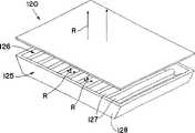
120,122: light changed course membrane system (substrate)
125: backlight
126: light source (array)
127: cold cathode fluorescent lamp
128,130: bearing
129: light emitting diode
BL: backlight (panel member)
D: display
I, I ': angle
R: light
T: penetrate through reflective device
Embodiment
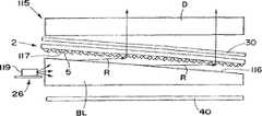
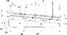
The 1st and 2 figure are light changed course membrane systems 1 that signal shows a kind of form according to the present invention, comprise light changedcourse film 2, its redistribution is by a backlight BL or more light that other light source sent and towards comparatively perpendicular to one of the surface offilm direction.Film 2 be can use with redistribution from the light of any light source almost within the visual angle of expectation, be used for the illumination for example a display D (such as: LCD), apply to laptop computer, word processor, aviation display, mobile phone, PDA(Personal Digital Assistant) and fellow, make display brighter.LCD can be any pattern person, comprising: as signal be shown in the 1st and 2 figure a kind of transmittance (transmissive) LCD, as signal be shown in the 3rd figure a kind of reflectivity (reflective) LCD and as signal be shown in a kind of penetrate through reflective (transflective) LCD of the 4th figure.
At the reflecting liquid crystal display D shown in the 3rd figure is to comprise being adjacent to one of dorsal part backreflector 40, be used to reflect enter this display around light and leave display to improve the brightness of this display.The present invention's light changedcourse film 2 is to put to being adjacent to the top of this reflecting liquid crystal display, with will around the light light of a front end light source (or from) be redirected to display and towards it more perpendicular to the direction on the plane of film, and withdrawing from visual angle in an expectation by the reflection of back reflector to improve the brightness of this display.Light changedcourse film 2 can be attached, stacking or is fixed in the top of LCD.
At the penetrate through reflective LCD D shown in the 4th figure is to comprise penetrate through reflective device (transflector) T who is placed between a display and the backlight BL, be used to reflect and enter that to hold light before the display be to withdraw from display improving in the brightness of the display of a bright light environments, and the light that is used to transport from this backlight withdraws from display to throw light in the display of a dark surrounds by this penetrate through reflective device.In this embodiment, light changedcourse film 2 is can put to the top that is adjacent to display or be the bottom that is adjacent to display or the two, be shown in the 4th figure as signal, be used to alter course or redistribute around light and/or from the light of backlight for more perpendicular to the plane of film, make light output be distributed as more to make us acceptance and improve the brightness of this display to advance by display.
Light changedcourse film 2 is to comprise a thin transparent membrane or asubstrate 8, it has one of otheroptical module 5 pattern that disperses that well defines shape and withdraws from surface 6 in the light of film, be used to reflect the distribution of light of incident, become more a direction perpendicular to the surface of film so that withdraw from the distribution of light of film.
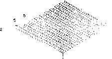
The various piece of individual otheroptical module 5 is to have less than one of the width of this film and length manyfold width and length, and can be by in the depression in the surface portion that withdraws from of film or teat and form.These otheroptical modules 5 are to comprise at least one inclined surface, and the light that is used to reflect incident is for towards the direction that withdraws from the surface perpendicular to light.The 5th figure is one of otheroptical module 5 pattern that is shown in a film 2.These optical modules are to take many different shapes.For example, 5a figure is theoptical module 5 that shows a non-prism, and it has twosurfaces 10,12 altogether, its two be inclination.On asurface 10 shown in the 5a figure are planes or smooth, and anothersurface 12 is crooked.Moreover two surfaces the 10, the 12nd intersect each other and also intersect at the surface of this film.Perhaps, twosurfaces 10,12 of individual other optical module can be bending, as be shown in 5b figure for signal.
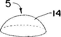
Perhaps,optical module 5 is the surfaces that can respectively only have a bending and inclination and intersect at film.5c figure is that display shape is one oftaper shape 13 this kindoptical module 5, and 5d figure shows another this kind optical module with hemisphere or domed shape 14.In addition, this kind optical module can have the inclined surface that surpasses and intersects at film.
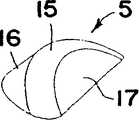
5e figure shows a kind ofoptical module 5 that has three surfaces altogether, and it is and intersects at film and for intersecting each other.Twosurfaces 15 and 16 are crooked, and the3rd surface 17 is smooth.
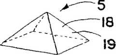
5f figure is that display shape is a kind ofoptical module 5 ofpyramid 18, and it has four leg-of-mutton sides 19 that intersect each other and intersect at film.Theside 19 ofpyramid 18 can be identical size and shape as in shown in the 5f figure, and perhaps, theside 19 ofpyramid 18 is to elongate, so these sides are the different peripheral shapes that have as shown in 5g figure.In addition,optical module 5 is the smooth inclined lateral side that can have any number.5h figure shows a kind ofoptical module 5 with four smooth inclinedlateral side 20, and 5i figure shows a kind ofoptical module 5 with eight smooth inclinedlateral side 20.
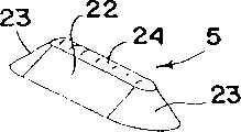
Individual otheroptical module 5 also can have above a curved surface and surpass a smooth inclined surface, and it all intersects at film.5j figure shows to have a pair ofsmooth side 22 of inclination and relative circle or bent back ends orside 23 that intersects relatively.Moreover thesmooth side 22 that tilts is the slope that can have different angles with bent back ends orside 23, as in shown in 5k and the 5l figure.Moreoveroptical module 5 is can have at least one curved surface not intersect at this film.This kindoptical module 5 is to be shown in 5m figure, and it comprises thesmooth side 22 of a pair of relative tilt, circle or bent back ends orside 23 and a circle or curvedtop portion 24 relatively, its crossing these relative tilt sides and relative circular distal.Moreoveroptical module 5 is can be along its curved in length, as in shown in the 5n figure.In addition, at least some surfaces ofoptical module 5 can be optically smooth, or have a texture, coating or apply other surface treatment, with the optical property that produces specific optical effect and/or special this light changed course film to be suitable for an application-specific.
Provide smooth and be combined in otheroptical module 5,, can alter course or redistribute a bigger visual angle compared to the film of a plough groove type with one of curved surface.In addition, the crooked area of the curvature on surface or indivedual optical modules is to change for the ratio of smooth area, distributes with the light output that is fit to film, is associated with the sight apparent area of one of film display device with the customization utilization.
It is to have an optics coating 25 (consulting the 2nd figure) that the light offilm 2 enters surface 7, such as: an antireflective coating, a reflection polarizer, are delayed coating, a polarization circulation coating or a polarizer.In addition, a tarnish or diffusion texture system can be arranged at light and enter surface 7, decide on desired visual appearance.The one lacklustre series of strata that are coated with produce softer image, but it is not brighter.The combination of the smooth and curved surface of indivedualoptical modules 5 of the present invention is can constitute with changed course bump some light thereon in different directions, need not to produce a comparatively soft image to enter one of surface extra diffusion or matt coating in film.
Also desirable, interlocking one staggered of indivedualoptical modules 5 of light changedcourse film 2 and/or the configuration of intersecting for being overlapped in each other, and foundation has a kind of optical texture of superior surf zone covering.For example, the 6th, 7,13 and 15 figure are that displayoptical assembly 5 is for crisscrossing each other; The the 8th to 10 figure is that displayoptical assembly 5 is for intersecting each other; And the 11st and 12 figure are that displayoptical assembly 5 is for interlocked with one another.
Moreover, angle of inclination, density, position, orientation, height or the degree of depth, shape and/or the size of the optical module 5 of light changed course film 2 is that the specific light output that can be matched with or be adjusted to a backlight BL or other light source distributes, with the variation of the distribution of considering the light of being launched by this backlight, more persons of the light of being launched by this backlight with redistribution are in the visual angle of an expectation.For example, the inclined surface of optical module 5 (for example: surface 10,12) can be along with backlight BL changes for increase from the distance of a light source 26 with the angle that the surface the made system of light changed course film 2, to consider this backlight along with the distance from light source serves as to increase to launch the mode of light R in different angles, as being shown in the 2nd figure for signal.In addition, backlight BL itself can be designed in the more light of lower angular emission, and improving the light amount of being launched by this backlight, and the more persons that rely upon the light that light changed course film 2 launched with redistribution are in the visual angle of an expectation.In this way, indivedual optical modules 5 of light changed course film 2 are can select to operate with the optical skew together with backlight, distribute to produce from the optimized output light angle of one of this system.
2nd, 5 and 9 figure are the different patterns that show the indivedualoptical modules 5 that are the equal height or the degree of depth, and the 7th, 8,10,13 and 14 figure are the different patterns that show indivedualoptical modules 5 of difformity, size and the height or the degree of depth.
Individual other optical module 5 also can be randomization in film 2, is shown in the 16th and 17 figure as signal, makes the pixel interference of exempting with a LCD at interval.This is the demand of exempting for the optical diffusion layer 30 shown in the 1st and 2 figure, to eliminate ripple and similar effect.Moreover, at least some person systems of individual other optical module 5 can be configured to the group 32 across film, in the optical module 5 of each group to have part at least be to have a different size or shape facilities, it is at each person of the group that changes across film and produce an average size or a shape facility together, as be shown in the 7th, 13 for signal, with 15 figure, to obtain surpassing the eigenwert of coupling tolerance deviation, to eliminate ripple and interference effect about LCD pixel interval.For example, be to have the different degree of depth or height in the part that has at least of the optical module 5 of each group 32, it is at each group that changes across film and collective produces the average degree of depth or an altitude feature.In addition, the optical module of each group to have part at least be to have a different pitch angle, it is at each group that changes across film and collective produces an average pitch angle.Moreover, at least one inclined surface cordings of indivedual optical modules of each group one different width or length being arranged, its collective produces an average width or length characteristic in each group that changes across film.
When individual other optical module 5 is to comprise the combination of one of flat surfaces 10, curved surface 12, the crooked area of the curvature of curved surface 12 or individual other optical module is to change for the ratio of smooth area and the peripheral shape of curved surface and flat surfaces, distributes with the light output that is fit to this film.In addition, the crooked area of the curvature of curved surface or individual other optical module is to change for the ratio of smooth area, with the changed course light more or less on a plane of the groove that is parallel to a prism or lens plough groove type film of advancing, and partially or completely replace needs for the light changed course film of a second layer.In addition, at least some of individual other optical module are can demarcate the orientation in relative to each other different angles, be shown in the 13rd and 16 figure as signal, the more rays of being launched by a light source with redistribution for along two disalignments in more perpendicular to the direction on the surface of film, and partially or completely replace the alter course needs of film of light for a second layer.Yet, will be for being understood that: identical or different pattern two layers this light changed course film thereon that respectively has indivedual optical modules 5, be to be placed between a light source and the sight viewed area, and these two layers revolve and turn 90 degrees (or greater than 0 degree less than other angle of 90 degree) each other, make in other optical module of separately thin layer redistribute by a light source launched and the more rays that navigates on the Different Plane direction in more perpendicular to the direction on the surface of separately film.
In addition, light changedcourse film 2 is to have one ofoptical module 5 pattern, it changes the diverse location in film, as being shown in the 15th figure for signal, distribute with the light output of redistribution, distribute from the light output of diverse location and towards perpendicular to one of film direction with redistribution from the diverse location of a backlight or other light source.
Moreover, the character and the pattern of the optical module of light changed course film can be customization, with at the light source of the different types of emission different light rays distributions and the optimization light film that alters course, for example: a pattern is aimed at single bulb laptop computer person, another pattern is aimed at two bulb flat-panel monitors, or the like.
The 17th figure is a configurations shown in from the outer ledge offilm 2 and towards theoptical module 5 of the radial pattern in one of center, distribute with the light output that redistributes a backlight BL, backlight BL system receives from the light along the coldcathode fluorescent lamp 26 of all four lateral edge of this backlight.
The 18th figure is a configurations shown across theoptical module 5 of one of thegroup 32 at the oblique angle offilm 2 pattern, it distributes with the light output that redistributes a backlight BL for special, and backlight BL receives from along the coldcathode fluorescent lamp 26 at one of this backlight input edge or the light of a plurality oflight emitting diode 26.
The 19th figure is theoptical module 5 of configurations shown in an one of corner of facingfilm 2 radiant type pattern, distributes with the light output that redistributes a backlight BL, and backlight BL is in corner by alight emitting diode 26 illuminations.The 20th figure is that configurations shown is in theoptical module 5 that regards to one of one offilm 2 input edge mid-points radiant type pattern, distribute with the light output that redistributes a backlight BL, backlight BL is by the mid point of singlelight emitting diode 26 illuminations in one of backlight input edge.
The 21st figure shows a kind of light changedcourse film 2, has theoptics groove 35 that extends in the face of one of film corner bending pattern across film, is distributed by the light output of alight emitting diode 26 illuminations in one of corner backlight BL with redistribution; And the 22nd to 24 figure shows a kind of light changedcourse film 2, has extension across film and in the face of a pattern along the optics groove 35 of one of film edge mid-points, it is along with the distance from this edge increases and reduce curvature, is distributed by the light output of one of the mid point that is positioned at the individual input of one of backlight edgelight emitting diode 26 illuminations in one of edge backlight BL with redistribution.
Be to have one of theoptical module 5 that changes along the length of thisfilm pattern 40 on light changedcourse film 2, thefilm 2 of onevolume 41 is to have one of optical module repeat patterns above can being set to, as for signal is shown in the 15th figure, to allow area that this pattern selects the most suitable application-specific with die-cut (diecut) film of this volume certainly.
Backlight BL is as expected and but essence is smooth or crooked, or can be single or multiple lift, and can have different-thickness and shape.Moreover backlight can be pliability or rigidity, and by being made by all compounds.Moreover backlight can be hollow and fills with liquid, gas, or is solid, and can have hole or spine (ridge).
In addition,light source 26 can be any suitable pattern, for example, it comprises: an arc lamp, an incandescent lamp (it also can be colour, filters or tints), a lens end bulb, a line lamp, a Halogen lamp LED, a light emitting diode (LED), from one of LED chip, a neon bulb, a cold cathode fluorescent lamp, carry from one of remote source optical fiber fluorescent tube, a laser or laser diode or any suitable light source.In addition,light source 26 can be the combination of one of the LED of polychrome or radiation source of polychrome, distributes with color or the white light output that an expectation is provided.For example, (for example: red, blue, green the lamp of a plurality of colors of) LED or single LED system with polychrome chip can use distributes with the light output that produces white light or any other color by the intensity that changes each colored light out of the ordinary such as different color.
One of optical skew pattern is can be arranged at as expected on one of backlight BL or two sides, or selects on zone in one or more of one of backlight or two sides.As for applying to this paper, term " optical skew " is meant that in any variation of the shape on a surface or geometric configuration and/or coating or surface treatment its light emission that causes a part is from this backlight.These distortion can various ways and make, for example, by the pattern of the pattern of the pattern that a coating is provided, an etched pattern, a processing, a pattern of printing, a hot pressing or a molded pattern or fellow in the zone of the selection of backlight.For example, printing ink or impressing pattern can be applied by pad printing, screen cloth printing, ink-jet, hot divert film processing or fellow.Distortion also can be printed on the film of skim, and it is deformed into backlight in order to apply this.This thin layer or film system can become the permanent part of one of backlight, for example by attached or locate this thin layer or film in one of backlight or two sides, to produce the effect of an expectation.
Rely on change on one or more zones of backlight or among density, opacity, translucence, shape, the degree of depth, color, area, refractive index or the pattern of distortion, the light output of controlling back light part.Distortion is can use with the percent of control from the light output of one of this backlight light-emitting zone.For example, distortion less and/or reduced size is to be placed in the surf zone of wanting less light output.Otherwise big number percent and/or bigger distortion system can be placed in the surf zone of the backlight of the big light output of expectation.
Change in the number percent and/or the size system of the distortion of the zones of different of backlight necessaryly, distribute in order to the uniform light output of essence to be provided.For example, advance the light by backlight amount near the zone of light source compared to farther shift out from other of light source regional bigger usually.The pattern of distortion is can use with at the light within backlight variation and adjust, and for example, along with the distortion of comparatively dense is provided from the distance of the increase of this light source, thereby causes the output of light comparatively uniformly from this backlight to distribute.
Distortion is also can use with the output x-ray angle of control from this backlight to distribute, to be applicable to an application-specific.For example, if this backlight is that utilization is with backlight illumination one LCD, if distortion (or light changedcourse film 2 is that utilization is combined in this backlight) is to guide the light of being launched by this backlight in a predetermined x-ray angle, by LCD, then light output is with more efficient so that it is with low loss.In addition, the pattern of optical skew is can use to adjust at the light output variation of drawing owing to the light of backlight.The pattern of optical skew can be printed on the backlight surf zone, and utilize scope be from smooth (glossy) to opaque (opaque) or the two coating widely, printing ink, coating, epoxy resin or fellow, and can use shadow tone (half-tone) isolation technics to change the coverage rate of this distortion.Moreover the pattern of optical skew can be multilayer or changes in refractive index.
The impressing pattern of optical skew system can change in shape, such as: point-like, square, diamond, ellipse, star, at random shape, similar therewith.In addition, the desirable every inch of utilization of going up is 60 row or trickleer impressing patterns.This is to make to be found in human eye hardly in the distortion or the shape of impressing pattern under an application-specific, thereby exempts the detecting of gradient or streak line, and the latter is for generally drawing pattern in the light that utilizes bigger assembly.In addition, distortion is can be along the length of backlight and/or width and change in shape and/or size.In addition, to put pattern at random be to be utilized as length and/or the width that spreads all in backlight in one of distortion.Distortion is to have the shape of no special angle or pattern, to reduce ripple or other interference effect.Produce these at random the example of the method for (random) pattern be the shape of printing a pattern, its utilization is (stochastic) impressing pattern technology, frequency modulating halftone pattern or random point shadow tone at random.Person very, distortion can be additive color, in order to implement the color correction of backlight.The color of distortion also can be changed to and spread all in backlight, for example, and so that the different color at identical or different light output area to be provided.
Be additional to or replace the pattern of optical skew, comprise prism or lensing groove or intersection trench or the more complicated shape of utilization other optical skew in the depressed part of the various shapes of a moulded pattern or the surface that raises, can be molded, etching, impression, thermoforming, hot pressing or fellow to one or more surf zone of backlight or on.Prism or lensing surface, depressed part or the surperficial system that raises will cause the light contact of a part, thereby for launching from this backlight.In addition, the variable-angleization on prism, depressed part or other surface distributes or effect with the light output that produces an expectation to guide light in different directions.Moreover reflectivity or refractivity surface are the shape or the patterns that can have no special angle, to reduce ripple or other interference effect.
Oneback reflector 40 is can be attached or be positioned one of backlight BL side, and as for signal is shown in the 1st and 2 figure, to improve the light output efficiency of backlight, its light of launching from this side by reflection passes through opposite side for returning by backlight for emission.In addition, one ofoptical skew 50 pattern is to be arranged at one of backlight side or two sides, as for signal is shown in the 1st and 2 figure, to change the path of light, makes that a part that surpasses inner critical angle and light is that emission is from one of backlight side or two sides.
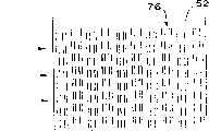
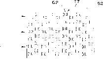
The the 25th to 28 figure is displayoptical distortion 50, and it can be in other teat 51 of separatelybacklight surf zone 52 or in other depressed part 53 of these surf zones.In each situation, each person of theseoptical skews 50 has a shape that well defines, comprise a reflectivity orrefractivity surface 54, it is that crossingbacklight surf zone 52 separately is in an edge 55, and have the slope that spreads all in the unanimity of its length, be used for more accurately controlling the light emission of each distortion.Along one of each reflectivity/refractivity surface 54 surrounding edge part 56 are one of eachdistortion 50 end walls 57, it is compared to the angle I ' between reflectivity/refractivity surface 54 and thepanel surface zone 52, be the panel surface zone 52 (consulting the 27th and 28 figure) of intersecting with a bigger angle I separately, so that be minimum in the projection surface zone of the end wall in this panel surface zone.This measure is to allowmore distortion 50 to be placed in the panel surface zone, compared to if the projection surface of end wall 57 zone is identical or can accomplish greater than the projection surface zone on reflectivity/refractivity surface 54 for essence.
In the 25th and 26 figure, reflectivity/refractivity surface 54 is in the horizontal direction bending with the surrounding edge part 56 of related end wall 57.In addition, at the 27th and 28 figure, the end wall 57 ofdistortion 50 is to show to extend to the reflectivity/refractivity surface 54 of essence perpendicular to these distortion.Perhaps, these end walls 57 be extensible for essence perpendicular topanel surface zone 52, as being shown in the 29th and 30 figure for signal.This is that essence is exempted any projection surface of end wall 57 zone is arranged onpanel surface zone 52, thus, is more to improve in the density of the distortion in panel surface zone.
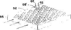
Optical skew also can be other shape that well defines, to obtain the light output distribution from the expectation of one of panel surf zone.The 31st figure is that other light that is shown in apanel surf zone 52 is drawndistortion 58, its each be comprise a reflectivity/refractivity surface 59 of summarizing smooth, rectangle, with spread all over related end wall 60 that its length and width are consistent slope, and be summarised as smooth sidewall 61.Perhaps, distortion 58 ' is to have circle orcurved sidewall 62, as being shown in the 32nd figure for signal.
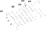
The 33rd figure is that other light that is shown in apanel surf zone 52 is drawndistortion 63, its each person be reflectivity/refractivity surface 64 of comprising one smooth, sloped triangular shape with related smooth, be summarised as leg-of-mutton sidewall or end wall 65.The 34th figure shows that other light draws distortion 66, and its each beend wall 69 and thesidewall 70 that comprises the oblique angle of one smooth, reflectivity/refractivity surface 67 of tilting and surroundingedge part 68 with oblique angle and association.
The 35th figure is that demonstration other light is drawndistortion 71, it is to be summarised as taper, and the 36th figure shows that other light drawsdistortion 72, and its each be the reflectivity/refractivity surface 73 that comprises a circle,circular end wall 74 and circle or curved sidewall 75 (mixing entirely).These extra surfaces be with reflection or its other light of going up of refraction bump on different directions, to scatter light for the more evenly distribution of the light of being launched from this panel member is provided across backlight/panel member BL.
Though individual other light draw distortion reflectivity/refractivity surface, end wall and sidewall given shape why, these distortion systems also can comprise flat surfaces, and it intersects these reflectivity/refractivity surface and end wall and/or sidewall with the relation that is parallel interval for panel surface zone 52.The the 37th to 39 figure shows distortion 76,77 and 78, its form has the representative shape that is similar to the they shown in the 31st, 32 and 35 figure respectively for other teat in a panel surf zone, except each distortion system is intersected by a flat surfaces 79 that is parallel spaced-apart relation for panel surface zone 52.In like manner, the 40th figure shows one of a plurality of distortion 80, and its form be individual other depressed part 81 in a panel surf zone 52, and each is to be one of the relation flat surfaces 79 of parallel interval and to be intersected by the summary flat surfaces for panel surface zone 52.If from the light emission in panel surface zone 52 with any light that strikes against these flat surfaces 79 less than the interior angle of critical angle is with by 79 internal reflections of flat surfaces, and will be launched by these flat surfaces with any light that strikes against these flat surfaces 79 greater than the interior angle of critical angle, and have minimum optics uncontinuity, as being shown in the 40th figure for signal.
When these distortion are teats onpanel surface zone 52, reflectivity/refractivity surface is to extend by one of panel direction and away from one of panel angle to be summarised as in contrast to advancing from the light oflight source 26, as being shown in the 27th and 29 figure for signal.When these distortion be depressed part in the panel surface zone, reflectivity/refractivity surface be with summary be same as from the light oflight source 26 advance by panel member direction and enter one of panel angle and extend, as being shown in the 28th and 30 figure for signal.
Though these distortion whether be on thepanel surface zone 52 or among teat or depressed part, the slope system on the light reflectivity/refractivity surface of these distortion can change, so that bump light thereon returns and passes through panel for reflecting self-emission panel or reflection, and launch opposite side from this panel, it can be etched to spread the light of being launched, or is covered by light changedcourse film 2, to produce an effect of expecting.In addition, can be consistently or variable at the pattern of the optical skew in panel surface zone, as expected, distribute from the light output of one of panel surface zone expectation obtaining.The 41st and 42figure show distortion 76 and 77, its shape is similar to the they shown in the 37th and 38 figure, and be disposed at along the length of apanel surf zone 52 and a plurality of even all row that separate at interval of straight line that are summarised as of width, and the 43rd and 44 figure are configurations shown thesedistortion 76 and 77 in staggered all row, and all row are to overlap each other along the length in panel surface zone.
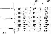
In addition, the size of optical skew (comprising: width, length, with the degree of depth or height) and angle orientation and position be to change along the length in any given panel surface zone and/or width, to obtain light output distribution from the expectation of one of this panel surface zone.The 45th and 46 figure be respectively display shape be similar to they's different size shown in the 31st and 32 figure distortion 58 and one of 58 ' at random or changeable pattern, it is disposed at staggered all row of a panel surf zone 52; And the 47th figure shows that its shape is similar to the distortion 77 of they shown in the 38th figure, along with the distance increase of distortion and light source or the intensity of light reduce and increase its size along the length in panel surface zone and/or width.In the distortion 58 and 58 ' shown in the 45th and 46 figure is to dispose across panel surface to troop (cluster) 82, in each at least some distortion of trooping is to have a different shape or size characteristics, and it is that collective produces at changing across each of panel surface one of troop average-size or shape facility.For example, in each at least some distortion of trooping is to have the different degree of depth or a height or a different slope or orientation, it is that collective produces an average degree of depth or an average gradient or the orientation of altitude feature or inclined surface, and it changes across panel surface.In like manner, can have a different width or a length in each at least some distortion systems of trooping, it is that collective changes across one of panel surface average width or length characteristic.This is to allow to obtain to surpass one of machining tolerance deviation desired size or shape facility, and also overcomes ripple and interference effect.
The 48th and 49 figure are that signal shows along the different angles orientation of theoptical skew 85 of any desired shape of the length of apanel surf zone 52 and width.In the 48th figure, distortion is allrow 86 that are disposed at along the straight line of the length in panel surface zone, but is that the orientation is in the face oflight source 26 in the distortion of each row, makes that all distortion are essence and launch from the light of light source in line.At the 49th figure,distortion 85 be similar to the 48th figure and also the orientation in the face of light source 26.In addition, the distortion in allrow 87 of the 49th figure is that essence is radially in alignment withlight source 26.
The 50th and 51 figure are that signal shows from inserting model or being cast in the light 90 of the example that one of a lighttransitional region 91 focusedlight source 26 of a kind of luminescent panel assembly BL according to the present invention launched, it how to reflect when advancing byluminescent panel member 92 up to strike against on thepanel surf zone 52 or among other light that well defines shape drawdistortion 50,77 till, cause more rays for reflection or reflect from one of thispanel member side 93 more than opposite side 94.In the 50th figure, the light 90 of example is to be shown as by reflectivity/54 on the refractivity surface ofdistortion 50 to reflect in the summary equidirectional, and exports thesame side 93 by panel member; And at the 51st figure, light 90 is display light line reflections/reflected before thesame side 93 of this panel member, by the different directions ofcircular sidewall 62 scatterings inpanel member 92 of distortion 77.The individual rays that well defines shape according to the present invention is drawn this kind pattern of distortion, is to make 60 to 70% or more persons through the light thatinput edge 95 received of panel member be the same side of emission from this panel member.
As discussed previously, other optical module of light changed course film is to be overlapped in one staggered, interlocking and/or crossing framework each other, has the surface coverage of increase and the axle that improves the light that withdraws from optics changed course film is gone up a kind of optical texture of gain with generation.The the 52nd to 55 figure is two kinds of indivedualoptical modules 5 that are shown in asurface 96 of an opticaltransparent substrate 8, its each smooth or plane only arrangedsurface 10 with only acurved surface 12 is arranged, it forms a spine (ridge) 97 jointly.In addition, thecurved surface 12 of optical module is to intersect each other, and with the otherwiseplanar surface area 10 that improves these optical modules relative number percent forcurved surface zone 12, and then the axle that improves the light by substrate is gone up and gained.The orientation of optometry assembly and position and decide, remaining otherwiseplanar surface area 10 of the optical module that intersects can be greater than 60% or even greater than 75% for the relative number percent in remainingcurved surface zone 12.
At theoptical module 5 shown in the 52nd to 55 figure is to summarize identical size and shape, and its orientation is for to regard to reverse direction withflat surfaces 10, and itscurved surface 12 is only arranged for intersecting each other.In addition, at the 52nd and 53 figure,optical module 5 is for directly in alignment with each other at Width; And at the 54th and 55 figure, optical module is for deviating from each other at Width.This departs from is to allow more persons of thecurved surface 12 of optical module not intersect theseflat surfaces 10 for intersecting each other, remaining otherwiseplanar surface area 10 of the feasible optical module that intersects is maximum for the relative number percent in remainingcurved surface zone 12, go up gain for maximum so that pass through the axle of the light of substrate, and the essence full surface of reaching at least one surface of the substrate that is occupied by optical module covers, for example: greater than 90% surface coverage.
The 56th figure is an one ofsurface 96optical module 5 that is shown in one of a kind of light changed course film opticaltransparent substrate 8, and it only has two sides orsurface 10 and 12, and it forms aspine 97 jointly, is similar to the optical module shown in the 52nd to 55 figure.Yet, be to have an asymmetric shape at the optical module shown in the56th figure.Side 10 and 12 is all to be shown as bending, and aside 12 is to have a less radius compared to another side 10.Two this kindoptical modules 5 are to be shown in the 57th and 58 figure, and compared to thanlong radius surface 10, twooptical modules 5 intersect each other to a bigger degree onsmall radii surface 12, reducing the 12 pairs of relative number percents thanlong radius surface 10 in small radii surface, and the axle that increases the light bysubstrate 8 is gone up and is gained.
Optical module 5 with interlockable geometric configuration also can locate and put with interlocked with one another, cover and do not intersect each other with the essence full surface at least one surface of reaching the substrate that is occupied by these optical modules, be shown in for example the 11st and 12 figure as signal.Yet, at least some persons ofoptical module 5 can have a geometric configuration, and it prevents that at least some optical modules from being interlocked with one another, as aflat surfaces 10 only being arranged when these optical modules and only having in thecurved surface 12, for example, as the 5th, 5a, with shown in 52 to 55 figure.If so, non-interlockableoptical module 5 is still can locate and put so that by the maximum that is covered as on the surface of the non-interlockable substrate that optical module occupied.
The 59th figure shows this kind configuration of one of non-interlockableoptical module 5, andoptical module 5 is location and puts to paired 98, and each to theflat surfaces 10 of optical module be the essence adjacency in alignment with each other.In addition, the all ofoptical module 5 is to be disposed at staggered allrow 99 to 98,curved surface 12 at each right optical module of each row is that essence is that tangent line is contacted with each other, and thecurved surface 12 in theoptical module 5 of each row is that essence is the curved surface that tangent line is contacted with the optical module of each adjacent column, with the high covering on the surface of reaching the substrate that is occupied by optical module.
Because the non-interlockable optical module 5 in the configuration shown in the 59th figure is not crossing, be to keep some not pattered region 100 between optical module.The number percent of pattered region 100 is not to specify by the configuration of special optical module 5.For example, the amount of the surf zone of patterning is not to reduce along with the interval of the optical module 5 that reduces Width and/or length direction, to cause optical module 5 for intersecting.Perhaps, the amount of pattered region 100 is not to be improved by the interval of the optical module that increases Width and/or length direction.This not pattered region 100 can be optically smooth, or have a texture (texture), coating or other surface treatment that applies, produce a specific optical effect and/or the optical property of special this light changed course film to be directed to special an application.This not pattered region 100 provide the functional of the combination that normally will need a plurality of optical thin films for a kind of mode that can use.For example, when another kind of light changed course film compared to the complete surface coverage of the essence with optical module 5, if the not pattered region of a film is to have light diffusion texture, it is that comparatively soft and visual angle this film will be increased that the light output of this film distributes, and the gain on the axle of this film is to reduce a little.This framework of this film is to provide the character of a light changed course film and a diffusion film in single film.
Moreover, the part that has at least ofoptical module 5 can be made up of the non-interlockable optical module of two difformities at least, its orientation and storing be not so that intersected each other by surface being covered as maximum of part being arranged of the substrate that optical module occupied, for example, as shown in the 8th and 14 figure.Or, at least some of non-interlockableoptical module 5 are also to can be the location to intersect each other to an either large or small degree, with the surface coverage amount of further increase by the non-interlockable substrate that optical module was occupied, be presented at the 60th figure as signal, so be that essence is complete (for example: complete for greater than 90%) by the covering of the non-interlockable surface element branch that optical module occupied.In addition, at least some persons of non-interlockableoptical module 5 can orientate (on theflat surfaces 10 of optical module) as to intersect each other oncurved surface 12 to a bigger degree, as being shown in the 61st figure for signal, the otherwise planar surface area of these non-interlockable optical modules that intersect is for the relative number percent in curved surface zone with further increase, and then increases the gain on the axle of the light by this substrate.
A kind of mode that constitutes these patterns of non-interlockable optical module is attached or assembles each non-interlockable optical module in an interlockable geometric configuration person, its patternable is in having one of complete surface coverage of essence two-dimentional lattice (lattice), and interlockable geometric configuration is the base shape of this lattice.The the 62nd to 64 figure shows three kinds of geometries.By choosing a suitable base shape, optical module is can make along with expectation to intersect or non-intersect.For example, be within thebase shape 101 that is contained in fully shown in the 62nd figure if not interlockableoptical module 5 is an essence, one of these optical modules pattern is to be non-intersect with essence.Otherwise if the actual boundary of should be non-interlockableoptical module 5 is to extend beyond as in thebase shape 102 or 103 shown in the 63rd or 64 figure, one of these optical modules pattern is will be crossing.
The the 59th to 61 figure is the example that shows the different pattern of non-interlockable wedge (wedge) the shapeoptical module 5 that is caused by the base shape 101-103 shown in the 62nd to 64 figure respectively.One light changed course film is that the percent surface coverage by the given pattern of non-interlockable optical module also can be easy to decision from this base shape.For example, in thebase shape 101 shown in the 62nd figure, non-interlockable optical module is to be about 91% in the projected area ratio ofbase shape 101 areas.Therefore, pattern is also to be about 91% for the percent on the surface of one of occupying light changed course film as the non-interlockable optical module as shown in the 59th figure covers.
Moreover in order to reduce ripple and other interference effect, a random disturbance (perturbation) is storing or the position that can introduce as for the non-interlockable optical module within this two dimension lattice.In order to prevent the generation of the extra not pattered region that randomization caused thus, the lattice that will introduce randomized all directions be at interval by greater than or the randomized amount of expectation that approximates an assigned direction compressed.This is to be equivalent at given non-interlockable optical module to choose a suitable less base shape (compared to not being utilization person if do not have randomization).
For example, choose in thebase shape 102 shown in the 63rd figure, at with the base shape of beginning at the beginning of shown in the 63rd figure randomization in a randomization version of one of width and length direction pattern, in case discern an initial pattern that suitably compresses, the position of at least some of then non-interlockable optical module is to be shifted by a random quantity of all directions of expectation randomization.Random quantity can be from the displacement accepted of a predetermined group and picked at random, or can be completely random.In each situation, be to set a upper limit in the random file amount (consistent) of an assigned direction, to avoid unacceptable patterning effects and to avoid introducing extra non-pattered region with the lattice decrement.The 65th and 66 figure are one of a derandominzation pattern 105 of the non-interlockableridged assembly 5 that shows that respectively processing is thus caused and a randomized patterns 106 examples.If extra non-pattered region is non-for paying close attention to subject under discussion or being sympathetic to a given application, then the compression at lattice interval is to carry out.
Except being patterned in single infrastructure component of a two-dimentional lattice, also can use to surpass an infrastructure component to produce more complicated lattice by the complete surface coverage of essence.Moreover the cancelled structure with the complexity that is less than the complete surface coverage of essence also can use.
Moreover, the radial pattern of one ofoptical module 5 be can be arranged on thesurface 96 of one of light changedcourse film 2 opticaltransparent substrate 8 or among, and optical module is to overlap each other and intersect, as being shown in the 67th figure for signal.
Desirable, the surface the 10, the 12nd of optical module 5, common formation uniqueness, non-circular spine 97 as for signal is shown in for example the 68th and 69 figure, upward gain to maximum so that withdraw from the axle of the light of this light changed course film.Yet, decide with the processing procedure of making light changed course film on its utilization, spine 97 is spine's sections 110 that can have one or more non-uniqueness (non-distinct), its can as signal be shown in the 70th and 72 figure 112 and be circular, but it more may be smooth for having, circular, crooked or distort the peak portion of spine 113 of (misshaped), be shown in the 71st and 73 figure as signal, this duplicates or forms owing to the incomplete of optical module shape.The incomplete of spine owing to optical module duplicates or forms, and is to allow this circle of spine 97 or the smooth or circular part of peak portion of spine, to use film as a brightness enhancing films.Yet, total sidewall surfaces long-pending (that is: the summation of the surface area of side or sidewall 10,12) for the total area of the side of optical module or sidewall and the peak portion of spine 113 of circular spine's section 112 or smooth, circular, crooked or distortion and ratio be to should be to be equal to or greater than 90%, as by being determined by following formula:
a)
Σi=1nAiΣi=1nAi+Σj=1mBj≥0.9
Wherein:
AiThe surface area of=thei sidewall 10,12, and
BjThe surface area of the peak portion of spine 113 of=the j circular spine cross section 112 or smooth, circular, crooked or distortion,
The number of n=sidewall 10,12,
The number of the peak portion of spine 113 of the spine cross section 112 of m=circle or smooth, circular, crooked or distortion.
Or, if peak portion of optical module spine total sidewall surfaces that to be total sidewall surfaces of existing of complete copy long-pending deducts it and do not exist because of the peak portion of spine 113 of circular spine cross section 112 or smooth, circular, crooked or distortion is amassed, with respect to if peak portion of optical module spine is a complete copy and total sidewall surfaces that will exist is amassed, be to should be to be equal to or greater than 90%, as being determined by following formula:
b)
Σi=1nαi-Σj=1mβjΣi=1nαi≥0.9
Wherein:
αiThe surface area of=thei sidewall 10,12 is complete formation or duplicates as ifspine 97, and
βj=the sidewall surfaces that do not exist because of the peak portion of spine 113 of j circular spine cross section 112 or smooth, circular, crooked or distortion is amassed,
The number of n=sidewall 10,12 is complete formation or duplicates as ifspine 97,
The number of the peak portion of spine 113 of the spine cross section 112 of m=circle or smooth, circular, crooked or distortion.
Specific, theoptical module 5 of the wedge shape of smooth for having, circular, the crooked or peak portion of spine 113 that distorts, as for being shown in for example the 73rd figure, the application of above-mentioned formula (b) provides the following stated person, and central utilization is given in the geometric definition of the 73rd figure.(that is: in the summation of the surface area of thesidewall 10,12 of the 68th figure) is to be given as if that peak portion of optical module spine is complete copy and total sidewall surfaces that will exist is long-pending:
c)(2-ξ)·sin(acos(ξ))+(1-2·ξ)·acos(ξ)
And the total sidewall surfaces that does not exist because of smooth, circular, the crooked or peak portion of spine 113 that distorts to amass be to be given as:
d)(2-β)·sin(acos(β))+(1-2·β)·acos(β)
Wherein:
ξ=1-γ2·R·cos(θ)β=1-DR·cos(θ)
The radius-of-curvature of R=curved sides 12,
The peak portion degree of depth of D=optical module 5 or height,
θ=smooth side 10 reaches for angle within thesurface 96 ofsubstrate 8
The width of γ=smooth, circular, the crooked or peak portion of spine 113 that distorts (for example: non-existent peak portion width), when looking it, as finding out in the 73 figure from the top and perpendicular to substrate.
Substitution formula (c) with (d) to following formula (b), then obtain following formula:
1-(2-ξ)·sin(acos(ξ))+(1-2·ξ)·acos(ξ)(2-β)·sin(acos(β))+(1-2·β)·acos(β)≥0.9
If it satisfy is meant: this light changed course film is can use as a brightness enhancing films.If peak portion of spine 113 is compared to this and more smooth, circular, crooked or distortion, this film may not be suitable for as a brightness enhancing films for most application, and is long-pending to obtain upward gain of axle fully because optical module shape system may not have enough sidewall surfaces.
The the 74th to 78 figure is other the light changed course membrane system 115 that shows according to the present invention, and it is summarised as and is similar to the shown light of the 1st and the 2 figure membrane system 1 that alters course.Yet, replace as the backlight BL as shown in the 1st and 2 figure with essence fixed thickness, the the 74th to 78 figure be icon be: backlight BL can be summarized as wedge shape, and its light-emitting area 116 is to increase and be convergent inwardly along its length along with the distance from light source 26.In addition, backlight BL can design so that light R withdraws from from backlight in extremely shallow angle.Because this measure, the different pattern of indivedual optical modules 5 be can be placed in that light enters on the surface 117 or among, as in shown in the 74th and 75 figure, if and expectation, the light that then can be placed in light changed course film 2 enter that surface 117 and light withdraw from that surface 117 ' is gone up or among, as in shown in the 76th figure, and be used to rotate the light R that is received from backlight BL, and cause light will pass through display with low loss in an acceptable angle, being directed to related display D (for example: it can be LCD), making the light system that launches by backlight.In addition, the relation that two light changed course film 2 can overlap each other and being placed between backlight BL and the related display D, wherein the different pattern of optical module 5 for enter in the light of a film on the surface 117 or among, and in the light of another film withdraw from that surface 117 ' is gone up or among (as in shown in the 77th figure), or enter on the surface 117 (as in shown in the 78 figure) in the light of two films.In the light source 26 shown in the 74th and 76 to 78 figure is a cold cathode fluorescent lamp 118, and is light emitting diodes 119 in the light source 26 shown in the 75th figure.
The 79th and 80 figure are the other light changedcourse membrane systems 120 and 122 that show according to the present invention, and it also summarizes the light changed course membrane system 1 that is similar to shown in the 1st and 2 figure.Yet, at changed course film of the light shown in the 79th and 80 figure orsubstrate 120 and 122 is to be covered in LCD TV backlight orother backlight 125, it can be made up oflight source array 126, is used to alter course and the moulding distribution from the light R of these backlight by the display (not shown).At the 79th figure,light source 126 is the coldcathode fluorescent lamp 127 that comprises an array, and it is fit to be installed on the bearing 128 of a dish case or kindred type; And in the 80th figure,light source 126 is thelight emitting diode 129 that comprises an array, and it is fit to be installed on the bearing 130 of a dish case or kindred type.Each light emitting diode is can have to be used to produce a color chips more than colour or the white light.
According to preamble, will be for being apparent that: more mostly being towards more perpendicular to the direction on the plane of film of the present invention's the light changed course film light that to be redistribution launched by a backlight or other light source.In addition, the present invention's light changed course film and backlight are to adjust special or each other, so that a kind of system to be provided, wherein, other optical module of light changed course film is together with in the optical skew of backlight and running produces from the optimized output light angle of one of this system and distributes.
Though the present invention shows about some embodiment and describes, is apparent that: the personage who is familiar with this skill will think in intensive reading and when understanding this instructions and the change and the modification of equivalence.Especially, about by the practiced all functions of above-mentioned member, the term that these members are described in utilization (comprising: any one " mechanism (means) " that touch upon) be to be intended to corresponding (unless indicating in addition) any member (for example: it is function equivalent) in the appointed function of carrying out described member, even non-structural equivalents is in the member of announcement of the function that is rendered in exemplary embodiment of the present invention described herein.In addition, although one of the present invention special characteristic is possible disclose about an embodiment is only arranged, this feature can be in conjunction with one or more further feature of other embodiment, and as can be expectation and help any given or specific application.

Claims (44)

9. light changed course film, comprise: an optical transparent substrate that approaches, its have a light enter the surface light relative with one withdraw from the surface, this light enters surface system and is used for the light of reception from a light source, at least one cording on these surfaces has one of indivedual optical modules of well defining shape pattern, these optical module cordings have at least two curved surfaces, one systems of the curved surface of these optical modules have a less radius compared to another curved surface, these optical modules are quite little for the length of this substrate and width, redistribute light and distribute by this substrate with a predetermined angular, wherein, on a curved surface of these optical modules, at least some persons of these optical modules intersect each other to a bigger degree, to reduce the relative percentage of one of these optical modules curved surface, with the gain on the axle that increases the light that passes through this substrate to another curved surface.
12. light changed course film, comprise: an optical transparent substrate that approaches, its have a light enter the surface light relative with one withdraw from the surface, this light enters surface system and is used for the light of reception from a light source, at least one cording on these surfaces has one of indivedual optical modules of well defining shape pattern, these optical module cordings have at least two inclined surfaces, and these optical modules are quite little for the length of this substrate and width, redistribute light and distribute by this substrate with a predetermined angular, wherein, at least some persons system of these optical modules intersects each other, and is that the complete surface coverage of essence is in this pattern of optical module with at least one of these surfaces of reaching this substrate.
19. light changed course film, comprise: an optical transparent substrate that approaches, its have a light enter the surface light relative with one withdraw from the surface, this light enters surface system and is used for the light of reception from a light source, at least one cording on these surfaces has one of indivedual optical modules of well defining shape pattern, these optical module cordings have at least two inclined surfaces, and these optical modules are quite little for the length of this substrate and width, redistribute light and distribute by this substrate with a predetermined angular, wherein, in this pattern of optical module, at least some part cordings in the zone on a surface of this substrate have not by one of these complete coverings of optical modules institute zone, are patterning not and stay this zone.
25. light changed course film, comprise: an optical transparent substrate that approaches, its have a light enter the surface light relative with one withdraw from the surface, this light enters surface system and is used for the light of reception from a light source, at least one cording on these surfaces has one of indivedual optical modules of well defining shape pattern, these optical modules are quite little for length of this substrate and width, redistribute light and distribute by this substrate with a predetermined angular, at least some persons of these optical modules are non-interlockable optical module, it has a geometric configuration is to prevent that these non-interlockable optical modules are interlocked with one another, these non-interlockable optical modules system location and putting serve as that expectation is covered in this pattern of non-interlockable optical module with at least one the part on these surfaces of producing this substrate.
43. light changed course film, comprise: an optical transparent substrate that approaches, its have a light enter the surface light relative with one withdraw from the surface, this light enters surface system and is used for the light of reception from a light source, at least one cording on these surfaces has one of indivedual optical modules of well defining shape pattern, and these optical modules are quite little for the length of this substrate and width, redistribute light and distribute by this substrate with a predetermined angular, only there are two sides or surface in these optical module systems, side be smooth and another side for crooked, this common spine that forms of two side systems, it is one smooth that this spine's cording has, circular, crooked, or the peak portion that distorts, wherein:
CN200580040648A2004-09-302005-09-28Light redirecting films and film systemsExpired - Fee RelatedCN100578291C (en)

Applications Claiming Priority (2)

Application NumberPriority DateFiling DateTitle
US10/954,5512004-09-30
US10/954,551US7364341B2 (en)1999-02-232004-09-30Light redirecting films including non-interlockable optical elements

Publications (2)

Publication NumberPublication Date
CN101164006Atrue CN101164006A (en)2008-04-16
CN100578291C CN100578291C (en)2010-01-06

Family

ID=36143011

Family Applications (1)

Application NumberTitlePriority DateFiling Date
CN200580040648AExpired - Fee RelatedCN100578291C (en)2004-09-302005-09-28Light redirecting films and film systems

Country Status (7)

CountryLink
US (4)US7364341B2 (en)
EP (2)EP2523035B1 (en)
JP (1)JP2008515026A (en)
KR (1)KR101095181B1 (en)
CN (1)CN100578291C (en)
TW (1)TWI362467B (en)
WO (1)WO2006039315A2 (en)

Cited By (10)

* Cited by examiner, † Cited by third party
Publication numberPriority datePublication dateAssigneeTitle
CN103037938A (en)*2010-08-172013-04-10皇家飞利浦电子股份有限公司Flexible light therapy device, a plaster and a bandage
WO2013155933A1 (en)*2012-04-162013-10-24山东新北洋信息技术股份有限公司Slice medium detector and slice medium processor
CN103688201A (en)*2011-05-202014-03-263M创新有限公司Light management film
CN104344352A (en)*2013-07-232015-02-11李政道Light guide device
CN106062467A (en)*2014-01-102016-10-26挪佛麦迪哥股份公司Lighting system
US9733411B2 (en)2012-10-312017-08-15Fluxwerx Illumination Inc.Light extraction elements
CN107430220A (en)*2015-04-082017-12-01株式会社可乐丽Complex diffuser
US10215344B2 (en)2012-03-052019-02-26Fluxwerx Illumination Inc.Light emitting panel assemblies and light guides therefor
TWI756905B (en)*2020-08-212022-03-01南韓商Lms股份有限公司 Optical film, backlight unit and liquid crystal display device
US11487151B2 (en)2019-08-292022-11-01Hefei Boe Display Technology Co., Ltd.Liquid crystal display panel and display device

Families Citing this family (151)

* Cited by examiner, † Cited by third party
Publication numberPriority datePublication dateAssigneeTitle
KR100965201B1 (en)*2001-06-122010-06-24웰스테트 테라퓨틱스 코포레이션 Compounds for the treatment of metabolic diseases
US7417782B2 (en)2005-02-232008-08-26Pixtronix, IncorporatedMethods and apparatus for spatial light modulation
TWI390251B (en)*2004-03-032013-03-21Kimoto Kk Light control film and the use of its backlight device
US7212345B2 (en)*2004-09-132007-05-01Eastman Kodak CompanyRandomized patterns of individual optical elements
WO2006052755A2 (en)*2004-11-042006-05-18Solid State Opto LimitedLong curved wedges in an optical film
US20060182409A1 (en)*2005-02-112006-08-17Eastman Kodak CompanyOptical films of differing refractive indices
US8519945B2 (en)2006-01-062013-08-27Pixtronix, Inc.Circuits for controlling display apparatus
US7502159B2 (en)2005-02-232009-03-10Pixtronix, Inc.Methods and apparatus for actuating displays
US7755582B2 (en)2005-02-232010-07-13Pixtronix, IncorporatedDisplay methods and apparatus
US7742016B2 (en)2005-02-232010-06-22Pixtronix, IncorporatedDisplay methods and apparatus
US7304785B2 (en)2005-02-232007-12-04Pixtronix, Inc.Display methods and apparatus
US7304786B2 (en)2005-02-232007-12-04Pixtronix, Inc.Methods and apparatus for bi-stable actuation of displays
US9229222B2 (en)2005-02-232016-01-05Pixtronix, Inc.Alignment methods in fluid-filled MEMS displays
US9087486B2 (en)2005-02-232015-07-21Pixtronix, Inc.Circuits for controlling display apparatus
US7616368B2 (en)2005-02-232009-11-10Pixtronix, Inc.Light concentrating reflective display methods and apparatus
US9082353B2 (en)2010-01-052015-07-14Pixtronix, Inc.Circuits for controlling display apparatus
US7999994B2 (en)2005-02-232011-08-16Pixtronix, Inc.Display apparatus and methods for manufacture thereof
US8159428B2 (en)2005-02-232012-04-17Pixtronix, Inc.Display methods and apparatus
US7746529B2 (en)2005-02-232010-06-29Pixtronix, Inc.MEMS display apparatus
US8310442B2 (en)2005-02-232012-11-13Pixtronix, Inc.Circuits for controlling display apparatus
US7271945B2 (en)2005-02-232007-09-18Pixtronix, Inc.Methods and apparatus for actuating displays
US9261694B2 (en)2005-02-232016-02-16Pixtronix, Inc.Display apparatus and methods for manufacture thereof
US9158106B2 (en)2005-02-232015-10-13Pixtronix, Inc.Display methods and apparatus
US7675665B2 (en)2005-02-232010-03-09Pixtronix, IncorporatedMethods and apparatus for actuating displays
US7405852B2 (en)2005-02-232008-07-29Pixtronix, Inc.Display apparatus and methods for manufacture thereof
US20070205969A1 (en)2005-02-232007-09-06Pixtronix, IncorporatedDirect-view MEMS display devices and methods for generating images thereon
US8482496B2 (en)2006-01-062013-07-09Pixtronix, Inc.Circuits for controlling MEMS display apparatus on a transparent substrate
US7113342B2 (en)*2005-02-242006-09-26Pong & Huang International Co., Ltd.Composite structure for light diffusion
US8596824B2 (en)*2005-05-242013-12-03Syncrolite, L.P.Method and apparatus for a scrollable modifier for a light fixture
US20060268558A1 (en)*2005-05-242006-11-30Synchrolite, L.P.Method and apparatus for controlling diffusion and color of a light beam
US8721123B2 (en)*2008-01-182014-05-13Syncrolite, LlcPattern generator for a light fixture
TWI351550B (en)*2005-06-092011-11-01Ubright Optronics CorpOptical substrate
US20070047228A1 (en)*2005-08-272007-03-013M Innovative Properties CompanyMethods of forming direct-lit backlights having light recycling cavity with concave transflector
KR101298786B1 (en)*2005-08-272013-08-22쓰리엠 이노베이티브 프로퍼티즈 컴파니Illumination assembly and system
US7537374B2 (en)*2005-08-272009-05-263M Innovative Properties CompanyEdge-lit backlight having light recycling cavity with concave transflector
US7815355B2 (en)*2005-08-272010-10-193M Innovative Properties CompanyDirect-lit backlight having light recycling cavity with concave transflector
WO2007067692A1 (en)*2005-12-062007-06-14Ubright Optronics CorporationLuminance enhancement optical substrates with anti-chatter structures
US7674028B2 (en)*2006-01-132010-03-09Avery Dennison CorporationLight enhancing structures with multiple arrays of elongate features of varying characteristics
US20070086207A1 (en)*2006-01-132007-04-19Optical Research AssociatesDisplay systems including light enhancing structures with arrays of elongate features
US7866871B2 (en)*2006-01-132011-01-11Avery Dennison CorporationLight enhancing structures with a plurality of arrays of elongate features
US8526096B2 (en)2006-02-232013-09-03Pixtronix, Inc.Mechanical light modulators with stressed beams
US7876489B2 (en)2006-06-052011-01-25Pixtronix, Inc.Display apparatus with optical cavities
RU2006119965A (en)*2006-06-072007-12-27Самсунг Электроникс Ко., Лтд. (KR) OPTICAL FILM
TW200801716A (en)*2006-06-272008-01-01Entire Technology Co LtdA high-brightness diffusion plate with trapezoid lens
TWI384260B (en)*2006-06-302013-02-01Ubright Optronics CorpLuminance enhancement optical substrates with optical defect masking structures
US7754041B2 (en)*2006-07-312010-07-133M Innovative Properties CompanyPleated filter with bimodal monolayer monocomponent media
US7643218B2 (en)*2006-08-312010-01-05Skc Haas Display Films Co., Ltd.Light redirecting film having varying optical elements
KR100835841B1 (en)*2006-09-062008-06-05주식회사 엘지화학 Condensing sheet and manufacturing method thereof
EP2080045A1 (en)2006-10-202009-07-22Pixtronix Inc.Light guides and backlight systems incorporating light redirectors at varying densities
CN101191863B (en)*2006-11-202012-02-01鸿富锦精密工业(深圳)有限公司 Preparation method of optical plate
US7661849B2 (en)*2006-11-272010-02-16Ping Sun Patrick LoIlluminated apparatus
US20100007934A1 (en)*2007-01-182010-01-14Sharp Kabushiki KaishaOptical Element and Image Display Device Using the Same
US7852546B2 (en)2007-10-192010-12-14Pixtronix, Inc.Spacers for maintaining display apparatus alignment
US9176318B2 (en)2007-05-182015-11-03Pixtronix, Inc.Methods for manufacturing fluid-filled MEMS displays
US20080188277A1 (en)2007-02-012008-08-07Ritter Janice EElectronic Game Device And Method Of Using The Same
US8842366B2 (en)*2007-05-112014-09-23Zetta Research and Development LLC—RPO SeriesTransmissive body
CN101373229B (en)*2007-08-202011-02-09鸿富锦精密工业(深圳)有限公司 Liquid crystal display device and prism sheet thereof
KR20090047926A (en)*2007-11-092009-05-13삼성전자주식회사 Backlight unit
JP2009176512A (en)*2008-01-232009-08-06Sony CorpSurface light source device and image display apparatus
US20110019436A1 (en)*2008-03-072011-01-27Koninklijke Philips Electronics N.V.Lighting system with removable light extracting member
US8248560B2 (en)2008-04-182012-08-21Pixtronix, Inc.Light guides and backlight systems incorporating prismatic structures and light redirectors
WO2010006102A2 (en)*2008-07-102010-01-143M Innovative Properties CompanyRetroreflective articles and devices having viscoelastic lightguide
US20110176325A1 (en)2008-07-102011-07-213M Innovative Properties CompanyViscoelastic lightguide
WO2010008070A1 (en)*2008-07-182010-01-21大日本印刷株式会社Optical sheet, surface light source device, and transmissive display device
US8462292B2 (en)*2008-07-312013-06-11Rambus Delaware LlcOptically transmissive substrates and light emitting assemblies and methods of making same, and methods of displaying images using the optically transmissive substrates and light emitting assemblies
US8205995B2 (en)*2008-08-072012-06-26Reflexite CorporationOptical device and system for privacy or contrast enhancement and methods of use thereof
US8169679B2 (en)2008-10-272012-05-01Pixtronix, Inc.MEMS anchors
DE102008055865A1 (en)2008-11-052010-05-12Lisa Dräxlmaier GmbHSensing device for operating electrical load in vehicle, particularly for integration in body trim, has fixed elastically deformed actuating surface, and flat elastically deformed light guide for illuminating symbolism
US20100128351A1 (en)*2008-11-212010-05-273M Innovative Properties CompanyCurved sided cone structures for controlling gain and viewing angle in an optical film
US8317352B2 (en)2008-12-112012-11-27Robert SaccomannoNon-invasive injection of light into a transparent substrate, such as a window pane through its face
US8361540B2 (en)*2008-12-162013-01-29Lockheed Martin CorporationRandomized circular grids for low-scatter EM shielding of a sensor window
CN101825736B (en)*2009-03-032013-07-24北京京东方光电科技有限公司Enhanced prism sheet
US7954983B2 (en)*2009-04-102011-06-07Entire Technology Co., Ltd.Optical component, manufacturing method of the same and backlight module
TWI388891B (en)*2009-05-142013-03-11Coretronic CorpLight guide plate and backlight module
US20100309409A1 (en)*2009-06-032010-12-09Starkey Kurt RLight emitting assemblies having defined regions of different brightness
EP2449414A1 (en)*2009-06-292012-05-093M Innovative Properties CompanyLightguide and light source incorporating same
EP2452218A1 (en)2009-07-092012-05-16Koninklijke Philips Electronics N.V.Free form lighting module
DE102009038469B4 (en)*2009-08-212015-02-12Advanced Display Technology Ag Display element and method for driving a display element
WO2011050982A1 (en)2009-10-292011-05-05Arno Martin SauerPlate for producing an led-illuminated sign
TWI400531B (en)*2009-12-232013-07-01Innolux CorpOptical plate and backlight module using the same
CN102844629B (en)*2010-01-132017-12-22诺尔斯海德公司For the manufacture method of the absorber coating of solar energy heating, such coating and its application
DE102010001359A1 (en)*2010-01-292011-08-04Zumtobel Lighting Gmbh Arrangement for influencing the light with a light-guiding element and a reflector element
KR20120132680A (en)2010-02-022012-12-07픽스트로닉스 인코포레이티드Methods for manufacturing cold seal fluid-filled display apparatus
US20110205756A1 (en)*2010-02-192011-08-25Pixtronix, Inc.Light guides and backlight systems incorporating prismatic structures and light redirectors
DE102010002282A1 (en)2010-02-242011-08-25Lisa Dräxlmaier GmbH, 84137 Interior trim part and outer trim part of a vehicle with an ultrasonic sensor
AT509563B1 (en)*2010-03-012015-10-15Hierzer Andreas LIGHT WITH LIGHTING ELEMENTS
US20120327312A1 (en)*2010-03-102012-12-27Sharp Kabushiki KaishaLighting device, display device and television receiver
US9180609B2 (en)*2010-03-262015-11-10Ubright Optronics CorporationOptical substrates having light collimating and diffusion structures
WO2011133745A1 (en)2010-04-212011-10-27Federal-Mogul Ignition CompanyReduced profile lamp having enhanced illumination and method of construction thereof
US8708520B2 (en)*2010-04-302014-04-29Seiko Epson CorporationIllumination device and electronic apparatus
DE102010019051A1 (en)*2010-05-032011-11-03Osram Opto Semiconductors Gmbh Area light guide and lighting device
US8735791B2 (en)2010-07-132014-05-27Svv Technology Innovations, Inc.Light harvesting system employing microstructures for efficient light trapping
KR20120014325A (en)*2010-08-092012-02-17삼성엘이디 주식회사 Optical lenses and lighting devices
US20150029744A1 (en)*2010-08-242015-01-29Unipixel Displays, Inc.Rotated micro-optical structures for banding suppression from point light sources
KR101866244B1 (en)*2011-01-172018-06-12삼성전자주식회사Scanning backlight unit and liquid crystal display having the same
KR20130025638A (en)*2011-09-022013-03-12엘지이노텍 주식회사 Optical sheet
TWM422634U (en)*2011-09-222012-02-11Arex Twn Internat Co LtdThe luminaire with uniformized luminous intensity
US9097826B2 (en)2011-10-082015-08-04Svv Technology Innovations, Inc.Collimating illumination systems employing a waveguide
US9019614B2 (en)*2011-10-262015-04-28Google Inc.Display device with image depth simulation
US9211481B2 (en)2012-07-272015-12-15Nb Tech Inc.Visual display system and method of constructing a high-gain reflective beam-splitter
WO2014058624A1 (en)*2012-10-082014-04-17Rambus Delaware LlcArticle of manufacture with micro-features of differing surface roughness
TWI478194B (en)*2012-12-192015-03-21Primax Electronics LtdLuminous keyboard
TWI478195B (en)*2012-12-192015-03-21Primax Electronics LtdLuminous keyboard
US9134552B2 (en)2013-03-132015-09-15Pixtronix, Inc.Display apparatus with narrow gap electrostatic actuators
US9110331B2 (en)2013-03-132015-08-18Vizio, Inc.Ultra-thin backlight for LCD displays through use of field-induced polymer electro luminescence panels including integrated light guide
US20140268879A1 (en)*2013-03-142014-09-18Panasonic CorporationTransparent waveguide diffuser for lighting and methods of manufacturing transparent waveguide diffuser
DE102013007938B4 (en)2013-05-072019-05-23Motherson Innovations Lights GmbH & Co. KG Flexible light guide and method of making a flexible light guide
JPWO2014181865A1 (en)*2013-05-102017-02-23株式会社クラレ Lighting device
TWI512372B (en)*2013-05-142015-12-11Innolux CorpBacklight module and display device
KR102030412B1 (en)*2013-05-312019-10-10엘지디스플레이 주식회사Light guide plate having rounded polyggon pattern and liquid cyrstal display device having thereof
EP3011372B1 (en)*2013-06-192021-12-08Bright View Technologies CorporationMicrostructure-based optical diffuser for creating batwing patterns and method for its manufacture
US10302275B2 (en)2013-06-192019-05-28Bright View Technologies CorporationMicrostructure-based diffusers for creating batwing lighting patterns
USD743091S1 (en)*2013-08-092015-11-10Acoustics First CorporationRipple diffuser
GB201315241D0 (en)2013-08-272013-10-09Nano Lit Technologies LtdImprovements in or relating to lighting
CN104460108B (en)*2013-09-222017-03-08纬创资通股份有限公司Backlight module
US10317583B2 (en)*2013-12-192019-06-11Bright View Technologies Corporation2D deglaring diffusers increasing axial luminous intensity
CN104848052A (en)*2014-02-132015-08-19扬升照明股份有限公司Backlight module
CN104932140B (en)2014-03-212017-12-26扬升照明股份有限公司Backlight module
US9411087B2 (en)*2014-03-272016-08-09Lg Display Co., Ltd.Backlight unit and liquid crystal display device having the same
US9645301B2 (en)*2014-03-282017-05-09Rambus Delaware LlcLighting assembly with edge-lit light guide and structured cover
FR3019263A1 (en)*2014-03-312015-10-02Valeo Vision OPTICAL GUIDE WITH PRISMATIC PATTERNS FORMING GALBAN DIOPTRES
US9703031B2 (en)*2014-04-282017-07-11Rambus Delaware LlcLight guide and lighting assembly with array of rotated micro-optical elements
WO2016019220A1 (en)*2014-07-312016-02-04Rambus Delaware LlcLight guide and lighting assembly with array of micro-optical element groupings
EP3194842A2 (en)*2014-07-312017-07-26Rambus Delaware LLCLight guide and lighting assembly having light redirecting features
CN106226849B (en)*2014-08-262019-03-01友辉光电股份有限公司Method for forming concave-convex structure on substrate and method for forming optical film
JP2016065964A (en)*2014-09-242016-04-28株式会社デンソーOptical component
WO2017147066A1 (en)*2016-02-222017-08-31Lumileds LlcAsymmetrical light intensity distribution from luminaire
WO2017214481A1 (en)*2016-06-102017-12-14Corning IncorporatedMicrostructured and patterned light guide plates and devices comprising the same
DE112017005617T5 (en)*2016-11-082019-09-12Denso Corporation Display device for vehicles
EP3563084A1 (en)*2016-12-292019-11-06Corning IncorporatedMicrostructured and patterned light guide plates and devices comprising the same
TWI612251B (en)2017-01-032018-01-21聯嘉光電股份有限公司Light emitting devices
US11137232B2 (en)*2017-01-132021-10-05Nielsen-Kellerman Co.Apparatus and method for indicating whether a target has been impacted by a projectile
JP6693452B2 (en)*2017-03-142020-05-13オムロン株式会社 Optical structure, light guide, and display device
DE102017003036A1 (en)*2017-03-292018-10-04Singulus Technologies Ag illuminant
USD888997S1 (en)2017-04-212020-06-30Acoustics First CorporationAcoustic panel
CN110537118B (en)*2017-04-272022-11-04索尼公司 Optical components, display devices and lighting devices
CN108882600B (en)*2017-05-162021-01-26昇印光电(昆山)股份有限公司Optical sheet, mold and electronic equipment cover plate
KR102782253B1 (en)2017-06-302025-03-17브라이트뷰 테크놀로지즈 아이엔씨. Light-transmitting structure for redistribution of light and lighting system comprising the light-transmitting structure
US11293725B2 (en)2017-07-112022-04-05Advanced Target Technologies Ip Holdings Inc.Method, system and apparatus for illuminating targets using fixed, disposable, self-healing reflective light diffusion systems
US10451264B2 (en)*2018-03-202019-10-22Tempo Industries, LlcWater resistant LED light fixtures
TWI680320B (en)*2019-02-222019-12-21達運精密工業股份有限公司Light guide plate
US11624495B2 (en)2019-05-202023-04-11Abl Ip Holding LlcSystems and methods for stabilizing optical sheets in luminaires
WO2020236971A1 (en)*2019-05-202020-11-26Abl Ip Holding LlcMicro-structured optical sheet and panel light assembly using same
US10921511B1 (en)*2019-09-062021-02-16The Boeing CompanyFloor lighting assembly
JP6912748B1 (en)*2020-02-072021-08-04日亜化学工業株式会社 Light emitting module and planar light source
JP7493149B2 (en)*2020-10-282024-05-31パナソニックIpマネジメント株式会社 Light-refractive components, optical systems, lighting systems, display systems, moving bodies and molds
CN115390179A (en)*2021-05-192022-11-25华为技术有限公司Light guide and near-to-eye display device
FI131598B1 (en)*2021-10-132025-08-01Nanocomp Oy Ltd LIGHT GUIDE
CN115016057B (en)*2022-08-032022-11-04北京驭光科技发展有限公司Diffractive light waveguide and display apparatus having the same
CN221079143U (en)2023-05-222024-06-04亮视技术公司 Backlight unit
US12372705B2 (en)*2023-07-122025-07-29Cm Visual Technology CorporationLight guide plate with asymmetrical optical microstructures

Family Cites Families (133)

* Cited by examiner, † Cited by third party
Publication numberPriority datePublication dateAssigneeTitle
US3070913A (en)1956-09-251963-01-01Miller Dial & Name Plate CompaEdge-lighted panel
US3049616A (en)*1958-03-061962-08-14Lighting Products IncPerforated lighting diffuser
US3043947A (en)*1960-04-081962-07-10Gen ElectricLight distributing lens system
US3532876A (en)*1963-10-171970-10-06Josef MullerLight fitting having at least one tubular lamp and a transparent covering of synthetic resin glass with a prismatic surface
US3267278A (en)*1965-02-241966-08-16Elastic Stop Nut CorpLens and lens assemblies
US3328570A (en)1965-04-091967-06-27Gen ElectricIlluminated panel member
US3543014A (en)1968-05-061970-11-24Farwest Electronics IncBuried panel-illuminating installation
US3571585A (en)1968-11-121971-03-23Coastal Dynamics CorpPanel and edge lighting assembly
DE1920071C3 (en)*1969-04-211979-07-19Trilux-Lenze Kg, 5760 Neheim-Huesten Luminaire with elongated lamps and a transparent cover
US3752974A (en)1971-12-131973-08-14Coastal Dynamics CorpUniform illumination with edge lighting
US3761703A (en)1971-12-231973-09-25U S Radium CorpApparatus for illumination of instrument faces
US3958113A (en)1973-04-261976-05-18Termohlen Carol ILighting effects device
US3892959A (en)1973-11-021975-07-01Gte Automatic Electric Lab IncEdge-lighted panel arrangement
US4043636A (en)1974-12-231977-08-23Intel CorporationIllumination-panel for liquid crystal display of similar device
CH604258B5 (en)1976-04-021978-08-31Ebauches Sa
US4183628A (en)1976-05-201980-01-15Ebauches S.A.Electronic watch and display device for such watch
US4114983A (en)*1977-02-181978-09-19Minnesota Mining And Manufacturing CompanyPolymeric optical element having antireflecting surface
US4177501A (en)1977-11-151979-12-04Harris CorporationIlluminated keyboard
US4282560A (en)1979-01-151981-08-04A.C.A. Products, Inc.Light distributor
US4257084A (en)1979-02-211981-03-17Reynolds Christopher HDisplay device
US4373282A (en)*1979-12-261983-02-15Hughes Aircraft CompanyThin-panel illuminator for front-lit displays
US4290093A (en)1980-03-201981-09-15Lite-A-Guide, Inc.Portable illuminated magazine case
US4460940A (en)1981-11-071984-07-17Kei MoriApparatus for uniform illumination employing light diffuser
US4446508A (en)1983-01-171984-05-01Plast-Ad, Inc.Edge lighted article holder
US4542449A (en)1983-08-291985-09-17Canadian Patents & Development LimitedLighting panel with opposed 45° corrugations
US4573766A (en)1983-12-191986-03-04Cordis CorporationLED Staggered back lighting panel for LCD module
JPS61127506U (en)1985-01-301986-08-11
US4630895A (en)1985-06-061986-12-23Motorola, Inc.LCD lightguide
US4714983A (en)1985-06-101987-12-22Motorola, Inc.Uniform emission backlight
US5056892A (en)1985-11-211991-10-15Minnesota Mining And Manufacturing CompanyTotally internally reflecting thin, flexible film
CA1279783C (en)1985-11-211991-02-05Minnesota Mining And Manufacturing CompanyTotally internally reflecting thin, flexible film
US4822145A (en)*1986-05-141989-04-18Massachusetts Institute Of TechnologyMethod and apparatus utilizing waveguide and polarized light for display of dynamic images
US4703405A (en)*1986-07-171987-10-27Ian LewinGlare reducing lens
US4751615A (en)1986-08-071988-06-14International Marketing Concepts, Inc.Page light
GB2196100B (en)1986-10-011990-07-04Mitsubishi Rayon CoLight diffusing device
US4763984A (en)1987-01-021988-08-16Awai George KLighting apparatus and method
US4765701A (en)1987-01-301988-08-23Poly-Optical Products, Inc.Illuminator optical fiber rod
US5005108A (en)1989-02-101991-04-02Lumitex, Inc.Thin panel illuminator
US4978952A (en)1989-02-241990-12-18Collimated Displays IncorporatedFlat screen color video display
US4974122A (en)1989-03-281990-11-27Rockwell International CorporationCompact LCD luminaire
US5667289A (en)1989-05-181997-09-16Seiko Epson CorporationBackground lighting apparatus for liquid crystal display
DE3919925A1 (en)1989-06-191990-12-20Inotec Gmbh Ges Fuer Innovativ ILLUMINATED, DISPLAY UNIT, PARTICULARLY HOUSE NUMBER, TRAFFIC SIGN, ADVERTISER
JPH0365982A (en)1989-08-031991-03-20Pioneer Electron CorpDisplay board illuminating device for display device
DE3929955A1 (en)1989-09-081991-03-14Inotec Gmbh Ges Fuer Innovativ LIGHT SPOTLIGHTS
US5283673A (en)1989-09-301994-02-01Kabushiki Kaisha Meitaku ShisutemuSurface luminous source panel with areas having different reflector speck densities
US4975808A (en)1989-10-021990-12-04Motorola, Inc.Backlighting apparatus
US5093765A (en)1990-02-161992-03-03Tosoh CorporationBack lighting device for a panel
US5101325A (en)1990-03-201992-03-31General Electric CompanyUniform illumination of large, thin surfaces particularly suited for automotive applications
DE69120349T2 (en)*1990-06-191996-10-31Enplas Corp Device for a flat light source
JP3204999B2 (en)1990-06-262001-09-04株式会社スタンレー滋賀製作所 Edge light panel
TW197499B (en)1990-07-031993-01-01Meitaku Syst Kk
DE69212662T2 (en)1991-02-211997-02-20Tosoh Corp Backlighting device
US5307244A (en)1991-07-011994-04-26Matthews Family Revocable TrustLight-insulated lamp and illuminating systems
EP0534140B1 (en)1991-08-221997-07-16Tosoh CorporationBacklighting device
US5349503A (en)1991-12-311994-09-20At&T Bell LaboratoriesIlluminated transparent display with microtextured back reflector
US5394255A (en)*1992-01-271995-02-28Sekisui Kagaku Kogyo Kabushiki KaishaLiquid crystal display using a plurality of light adjusting sheets angled at 5 degrees or more
US5303322A (en)1992-03-231994-04-12Nioptics CorporationTapered multilayer luminaire devices
US5237641A (en)*1992-03-231993-08-17Nioptics CorporationTapered multilayer luminaire devices
CA2097109C (en)1992-06-012000-01-11Shozo KokawaLiquid crystal display
JPH0651129A (en)1992-07-271994-02-25Inoue Denki KkIlluminating device
JP2601766Y2 (en)1992-08-311999-12-06日本電産コパル株式会社 Surface emitting device
JP3006306B2 (en)1992-09-162000-02-07インターナショナル・ビジネス・マシーンズ・コーポレイション Optical film and liquid crystal display device using the optical film
JPH0695112A (en)1992-09-161994-04-08Hitachi LtdPrism plate and information display device formed by using this plate
US5339179A (en)1992-10-011994-08-16International Business Machines Corp.Edge-lit transflective non-emissive display with angled interface means on both sides of light conducting panel
US5386347A (en)1992-10-021995-01-31Photo Craft Co., Ltd.Illuminating apparatus and a method of manufacturing an edge light conductor for use therein
JP2630714B2 (en)1992-10-081997-07-16茶谷産業株式会社 Surface lighting device
US5396406A (en)*1993-02-011995-03-07Display Technology IndustriesThin high efficiency illumination system for display devices
US5581605A (en)*1993-02-101996-12-03Nikon CorporationOptical element, production method of optical element, optical system, and optical apparatus
JPH07113718B2 (en)1993-03-031995-12-06日本電気株式会社 Backlight device for liquid crystal panel
US5598280A (en)1993-03-231997-01-28Dai Nippon Printing Co., Ltd.Film lens and a surface light source using the same
US5475533A (en)*1993-08-021995-12-12Applied Physics Research, L.P.Apparatus for enhancing the brightness of an image and method of making the same
US5396350A (en)1993-11-051995-03-07Alliedsignal Inc.Backlighting apparatus employing an array of microprisms
US6129439A (en)*1993-11-052000-10-10Alliedsignal Inc.Illumination system employing an array of multi-faceted microprisms
US5598281A (en)1993-11-191997-01-28Alliedsignal Inc.Backlight assembly for improved illumination employing tapered optical elements
US5390085A (en)1993-11-191995-02-14Motorola, Inc.Light diffuser for a liquid crystal display
US5485291A (en)1994-02-221996-01-16Precision Lamp, Inc.Uniformly thin, high efficiency large area lighting panel with two facet grooves that are spaced apart and have light source facing facets with smaller slopes than the facets facing away from the light source
US5982540A (en)1994-03-161999-11-09Enplas CorporationSurface light source device with polarization function
JP3538220B2 (en)1994-05-252004-06-14株式会社エンプラス Corner light supply type surface light source device
US5719649A (en)1994-06-081998-02-17Kabushiki Kaisha ToshibaLight guide and liquid crystal display device using it
US5671994A (en)1994-06-081997-09-30Clio Technologies, Inc.Flat and transparent front-lighting system using microprisms
US5575549A (en)1994-08-121996-11-19Enplas CorporationSurface light source device
US5808784A (en)1994-09-061998-09-15Dai Nippon Printing Co., Ltd.Lens array sheet surface light source, and transmission type display device
DE69532771T2 (en)1994-09-272004-09-30Minnesota Mining And Mfg. Co., St. Paul Luminance control film
US5506929A (en)1994-10-191996-04-09Clio Technologies, Inc.Light expanding system for producing a linear or planar light beam from a point-like light source
JP3544010B2 (en)1994-10-252004-07-21本田技研工業株式会社 Vehicle lighting
AU4409496A (en)1994-11-291996-06-19Precision Lamp, Inc.Edge light for panel display
US5579134A (en)1994-11-301996-11-26Honeywell Inc.Prismatic refracting optical array for liquid flat panel crystal display backlight
US5521342A (en)1994-12-271996-05-28General Motors CorporationSwitch having combined light pipe and printed circuit board
AU694619B2 (en)1995-03-031998-07-23Minnesota Mining And Manufacturing CompanyLight directing film having variable height structured surface and light directing article constructed therefrom
US5576078A (en)1995-03-271996-11-19Schatz; Alan G.Illuminated christmas ornament
US5618095A (en)1995-04-041997-04-08Tosoh CorporationBacklighting device
US6712481B2 (en)1995-06-272004-03-30Solid State Opto LimitedLight emitting panel assemblies
US5613751A (en)1995-06-271997-03-25Lumitex, Inc.Light emitting panel assemblies
US5590945A (en)1995-07-261997-01-07Industrial Devices, Inc.Illuminated line of light using point light source
WO1997004940A1 (en)1995-07-281997-02-13Nippon Carbide Kogyo Kabushiki KaishaMicroprism matrix
JP3607759B2 (en)1995-09-082005-01-05五洋紙工株式会社 Prism sheet
JPH09105804A (en)1995-10-131997-04-22Konica CorpLight control sheet, surface light source device, and liquid crystal display device
US6011602A (en)1995-11-062000-01-04Seiko Epson CorporationLighting apparatus with a light guiding body having projections in the shape of a trapezoid
US5695269A (en)1996-01-291997-12-09Delco Electronics CorporationMulti-color display lighting by led
US5961198A (en)*1996-02-021999-10-05Hitachi, Ltd.Liquid crystal display device and method of manufacturing backlighting light guide panel therefor
US5917664A (en)1996-02-051999-06-293M Innovative Properties CompanyBrightness enhancement film with soft cutoff
US5838403A (en)*1996-02-141998-11-17Physical Optics CorporationLiquid crystal display system with internally reflecting waveguide for backlighting and non-Lambertian diffusing
JP3328132B2 (en)*1996-03-212002-09-24株式会社ユニシアジェックス Inhaler type dispenser
US5919551A (en)1996-04-121999-07-063M Innovative Properties CompanyVariable pitch structured optical film
TW331593B (en)1996-05-131998-05-11Konika Co LtdPlaner light source device and light guide plate
TW368610B (en)1996-09-241999-09-01Seiko Epson CorpLighting device and the display monitor employing the lighting device
EP1666934A1 (en)1996-10-252006-06-07Omron CorporationSurface light source device and liquid crystal display device, portable telephone and information terminal using surface light source device
US5913594A (en)1997-02-251999-06-22Iimura; KeijiFlat panel light source device and passive display device utilizing the light source device
JPH10260315A (en)*1997-03-171998-09-29Dainippon Printing Co Ltd Lens light guide plate and surface light source device using the same
US6280063B1 (en)1997-05-092001-08-283M Innovative Properties CompanyBrightness enhancement article
EP1975649A1 (en)1998-02-182008-10-01Minnesota Mining And Manufacturing CompanyOptical film
JP3297846B2 (en)*1998-03-052002-07-02ミネベア株式会社 Transmission type surface illumination device
JPH11305011A (en)*1998-04-221999-11-05Dainippon Printing Co Ltd Lens film and surface light source device
KR100271672B1 (en)1998-05-202000-11-15구본준Sheet type optical device and backlight unit using the same
US6124975A (en)*1998-09-182000-09-26U.S. Philips CorporationLenticular sheet
TW579438B (en)*1999-02-042004-03-11Keiwa IncLight diffusion plate and backlight device using the same
US6752505B2 (en)1999-02-232004-06-22Solid State Opto LimitedLight redirecting films and film systems
US6827456B2 (en)1999-02-232004-12-07Solid State Opto LimitedTransreflectors, transreflector systems and displays and methods of making transreflectors
US6213625B1 (en)*1999-04-232001-04-10Nsi Enterprises, Inc.Inverted apex prismatic lens
KR100323827B1 (en)*1999-06-072002-02-19구본준, 론 위라하디락사Backlight device
JP2000352607A (en)*1999-06-112000-12-19Dainippon Printing Co Ltd Light diffusion film, manufacturing method thereof, surface light source, and display device
US6277471B1 (en)*1999-06-182001-08-21Shih Chieh TangBrightness enhancement film
US6356391B1 (en)*1999-10-082002-03-123M Innovative Properties CompanyOptical film with variable angle prisms
JP4408166B2 (en)*2000-04-272010-02-03大日本印刷株式会社 Directional diffusion film and manufacturing method thereof, surface light source device and liquid crystal display device
JP4266551B2 (en)*2000-12-142009-05-20三菱レイヨン株式会社 Surface light source system and light deflection element used therefor
WO2002077672A2 (en)*2001-02-072002-10-03Corning IncorporatedHigh-contrast screen with random microlens array
KR20050044695A (en)*2001-12-052005-05-12솔리드 스테이트 옵토 리미티드Transreflectors, transreflector systems and displays and methods of making transreflectors
TW594108B (en)*2002-06-242004-06-21Mitsubishi Rayon CoLight source device and light deflection element
JP4030835B2 (en)*2002-08-232008-01-09アルプス電気株式会社 Reflector and reflective liquid crystal display device including the reflector
US6859326B2 (en)*2002-09-202005-02-22Corning IncorporatedRandom microlens array for optical beam shaping and homogenization
US20040062031A1 (en)*2002-09-302004-04-01Matt PinterIlluminated shelf
TW575185U (en)*2002-11-152004-02-01Hon Hai Prec Ind Co LtdBacklight system and light guide plate thereof
US7212345B2 (en)2004-09-132007-05-01Eastman Kodak CompanyRandomized patterns of individual optical elements

Cited By (19)

* Cited by examiner, † Cited by third party
Publication numberPriority datePublication dateAssigneeTitle
CN103037938A (en)*2010-08-172013-04-10皇家飞利浦电子股份有限公司Flexible light therapy device, a plaster and a bandage
CN103037938B (en)*2010-08-172016-05-25皇家飞利浦电子股份有限公司Flexible phototherapy device, plaster and bandage
CN103688201A (en)*2011-05-202014-03-263M创新有限公司Light management film
US10215344B2 (en)2012-03-052019-02-26Fluxwerx Illumination Inc.Light emitting panel assemblies and light guides therefor
WO2013155933A1 (en)*2012-04-162013-10-24山东新北洋信息技术股份有限公司Slice medium detector and slice medium processor
CN103376476A (en)*2012-04-162013-10-30山东新北洋信息技术股份有限公司Sheet type medium detecting device and sheet type medium processing device
CN103376476B (en)*2012-04-162016-06-08山东新北洋信息技术股份有限公司Flaky medium detecting device and laminated medium processing unit
US9733411B2 (en)2012-10-312017-08-15Fluxwerx Illumination Inc.Light extraction elements
US9823406B2 (en)2012-10-312017-11-21Fluxwerx Illumination Inc.Light extraction elements
CN104344352B (en)*2013-07-232017-10-03李政道Light guide device
CN104344352A (en)*2013-07-232015-02-11李政道Light guide device
CN106062467A (en)*2014-01-102016-10-26挪佛麦迪哥股份公司Lighting system
US10338301B2 (en)2014-01-102019-07-02Novomatic AgLighting system
CN107430220A (en)*2015-04-082017-12-01株式会社可乐丽Complex diffuser
US10877188B2 (en)2015-04-082020-12-29Kuraray Co., Ltd.Composite diffuser plate
CN107430220B (en)*2015-04-082021-03-09株式会社可乐丽Composite diffusion plate
US11487151B2 (en)2019-08-292022-11-01Hefei Boe Display Technology Co., Ltd.Liquid crystal display panel and display device
TWI756905B (en)*2020-08-212022-03-01南韓商Lms股份有限公司 Optical film, backlight unit and liquid crystal display device
US11442204B2 (en)2020-08-212022-09-13Lms Co., Ltd.Optical film

Also Published As

Publication numberPublication date
JP2008515026A (en)2008-05-08
TWI362467B (en)2012-04-21
TW200615491A (en)2006-05-16
US20130107543A1 (en)2013-05-02
EP2523035A1 (en)2012-11-14
KR101095181B1 (en)2011-12-16
US20080138024A1 (en)2008-06-12
WO2006039315A3 (en)2007-06-07
US20050122591A1 (en)2005-06-09
CN100578291C (en)2010-01-06
EP1794639A4 (en)2010-03-10
US20100188858A1 (en)2010-07-29
US7364341B2 (en)2008-04-29
US8668371B2 (en)2014-03-11
US7712932B2 (en)2010-05-11
WO2006039315A2 (en)2006-04-13
EP2523035B1 (en)2016-04-27
EP1794639A2 (en)2007-06-13
US8398274B2 (en)2013-03-19
KR20070061901A (en)2007-06-14

Similar Documents

PublicationPublication DateTitle
CN100578291C (en)Light redirecting films and film systems
CN100432717C (en)Light redirecting films and film systems
US7134778B2 (en)Resembling prismatic structure of light guide plate
CN108388047A (en)Backlight module and display device
EP4051957B1 (en)Lighting device for providing a sparkling appearance
CN218630255U (en)Diffusion film

Legal Events

DateCodeTitleDescription
C06Publication
PB01Publication
C10Entry into substantive examination
SE01Entry into force of request for substantive examination
C14Grant of patent or utility model
GR01Patent grant
ASSSuccession or assignment of patent right

Owner name:SOLID OPTO CO., LTD.

Free format text:FORMER OWNER: SOLID STATE OPTO LTD.

Effective date:20110209

C41Transfer of patent application or patent right or utility model
CORChange of bibliographic data

Free format text:CORRECT: ADDRESS; FROM: SHANGHAI, CHINA TO: TORTOLA, BRITISH VIRGIN ISLANDS

TR01Transfer of patent right

Effective date of registration:20110209

Address after:The British Virgin Islands

Patentee after:Solid state opto Co. Ltd.

Address before:Shanghai China

Patentee before:Solid State Opto Ltd.

ASSSuccession or assignment of patent right

Owner name:RAMBUS INTERNATIONAL LTD.

Free format text:FORMER OWNER: SOLID OPTO CO., LTD.

Effective date:20110714

C41Transfer of patent application or patent right or utility model
CORChange of bibliographic data

Free format text:CORRECT: ADDRESS; FROM: TORTOLA, BRITISH VIRGIN ISLANDS TO: GRAND CAYMAN, CAYMAN ISLANDS (BRITISH)

TR01Transfer of patent right

Effective date of registration:20110714

Address after:The Cayman Islands (British) Grand Cayman

Patentee after:Solid State Opto Ltd.

Address before:The British Virgin Islands

Patentee before:Solid state opto Co. Ltd.

CF01Termination of patent right due to non-payment of annual fee

Granted publication date:20100106

Termination date:20140928

EXPYTermination of patent right or utility model

[8]ページ先頭

©2009-2025 Movatter.jp