CN101163440B - Three-dimensional adhesive device with embedded microelectronic system - Google Patents
Three-dimensional adhesive device with embedded microelectronic systemDownload PDFInfo
- Publication number
- CN101163440B CN101163440BCN2006800137188ACN200680013718ACN101163440BCN 101163440 BCN101163440 BCN 101163440BCN 2006800137188 ACN2006800137188 ACN 2006800137188ACN 200680013718 ACN200680013718 ACN 200680013718ACN 101163440 BCN101163440 BCN 101163440B
- Authority
- CN
- China
- Prior art keywords
- adhesive
- adhesive device
- binding agent
- parts
- microelectronics system
- Prior art date
- Legal status (The legal status is an assumption and is not a legal conclusion. Google has not performed a legal analysis and makes no representation as to the accuracy of the status listed.)
- Expired - Fee Related
Links
Images


Classifications
- A—HUMAN NECESSITIES
- A61—MEDICAL OR VETERINARY SCIENCE; HYGIENE
- A61B—DIAGNOSIS; SURGERY; IDENTIFICATION
- A61B5/00—Measuring for diagnostic purposes; Identification of persons
- A61B5/68—Arrangements of detecting, measuring or recording means, e.g. sensors, in relation to patient
- A61B5/6801—Arrangements of detecting, measuring or recording means, e.g. sensors, in relation to patient specially adapted to be attached to or worn on the body surface
- A61B5/683—Means for maintaining contact with the body
- A61B5/6832—Means for maintaining contact with the body using adhesives
- A61B5/6833—Adhesive patches
- A—HUMAN NECESSITIES
- A61—MEDICAL OR VETERINARY SCIENCE; HYGIENE
- A61B—DIAGNOSIS; SURGERY; IDENTIFICATION
- A61B5/00—Measuring for diagnostic purposes; Identification of persons
- A61B5/41—Detecting, measuring or recording for evaluating the immune or lymphatic systems
- A61B5/411—Detecting or monitoring allergy or intolerance reactions to an allergenic agent or substance
Landscapes
- Health & Medical Sciences (AREA)
- Life Sciences & Earth Sciences (AREA)
- Medical Informatics (AREA)
- Biophysics (AREA)
- Pathology (AREA)
- Engineering & Computer Science (AREA)
- Biomedical Technology (AREA)
- Heart & Thoracic Surgery (AREA)
- Physics & Mathematics (AREA)
- Molecular Biology (AREA)
- Surgery (AREA)
- Animal Behavior & Ethology (AREA)
- General Health & Medical Sciences (AREA)
- Public Health (AREA)
- Veterinary Medicine (AREA)
- Immunology (AREA)
- Vascular Medicine (AREA)
- Adhesives Or Adhesive Processes (AREA)
Abstract
Description
Translated fromChinese技术领域technical field
本发明涉及主要用于监视生理或神经条件的微电子系统。更特别地,本发明涉及被嵌入三维粘合剂器件中的侵入式和非侵入式微电子系统,该三维粘合剂器件可被附着到哺乳动物的表面上,该表面适当地为皮肤。该微电子系统适当地利用无线通信并可用于测量ECG(心电图)、EMG(肌电图)、EEG(脑电图)、血糖、脉搏、血压、pH值和氧。The present invention relates to microelectronic systems primarily for monitoring physiological or neurological conditions. More particularly, the present invention relates to invasive and non-invasive microelectronic systems embedded in a three-dimensional adhesive device that can be attached to a mammalian surface, suitably skin. The microelectronic system suitably utilizes wireless communication and can be used to measure ECG (electrocardiogram), EMG (electromyography), EEG (electroencephalogram), blood glucose, pulse, blood pressure, pH and oxygen.
背景技术Background technique
感测系统通过压敏粘合剂向皮肤的附着被很好地建立。因此,AMBU A/S,DK具有大量的用于测量ECG的产品,这些产品通过泡沫粘合剂、微孔粘合剂或水凝胶粘合剂附着到皮肤上。这些传感器一般通过导线连接到监视设备上。The sensing system is well established by attachment of pressure sensitive adhesives to the skin. Therefore, AMBU A/S, DK has a large number of products for measuring ECG which are attached to the skin by foam adhesives, microporous adhesives or hydrogel adhesives. These sensors are generally connected to monitoring equipment by wires.
在WO 03/065926A2中,Ozgus等人公开了具有柔软并且较薄的集成电路的可佩带的生物监视器。该专利申请提出通过使用薄层粘合剂或粘合剂垫料附着到皮肤上而实现高舒适度佩带的方式。但是,使用的粘合剂是吸留的。该申请还说明了用于无线数据收集的传感器模块,该传感器模块具有包含电路的薄硅板和作为多个层被嵌入传感器模块内的柔性电源。In WO 03/065926A2, Ozgus et al. disclose a wearable biomonitor with flexible and thinner integrated circuits. This patent application proposes a way of achieving a high wearing comfort by attaching to the skin using a thin layer of adhesive or an adhesive pad. However, the adhesive used is occlusive. The application also describes a sensor module for wireless data collection with a thin silicon plate containing circuitry and a flexible power source embedded as multiple layers within the sensor module.
在US 5054488中,Mus等人公开了用于产生代表生理条件的电信号的光电子传感器。传感器可通过聚酯衬里上的双侧压敏粘合剂被附着到身体上。In US 5054488, Mus et al. disclose optoelectronic sensors for generating electrical signals representative of physiological conditions. The sensor can be attached to the body by double sided pressure sensitive adhesive on the polyester liner.
在US 5458124中,Stanko等人公开了通过双侧压敏粘合剂被附着到身体上的心电图电极。In US 5458124, Stanko et al. disclose electrocardiogram electrodes that are attached to the body by a double sided pressure sensitive adhesive.
在US 6372951中,Ter-Ovanesyan等人公开了在操作上连接到通过粘合剂补片与佩带者配合的一次性物品上的传感器。各种各样的身体粘合成分可被使用。In US 6372951, Ter-Ovanesyan et al. disclose sensors operatively attached to a disposable item that is fitted to the wearer by an adhesive patch. A wide variety of body bonding compositions can be used.
在US 6385473中,Haines等人公开了用水解胶体粘合剂的两个条带附着到哺乳动物对象身体上的层叠的传感器器件。层叠结构也包含与水解胶体粘合剂接触的水凝胶。器件的寿命规定为24小时。In US 6385473, Haines et al. disclose a laminated sensor device attached to the body of a mammalian subject with two strips of hydrocolloid adhesive. The laminated structure also comprises a hydrogel in contact with a hydrocolloid binder. The lifetime of the device is specified as 24 hours.
在WO 99/59465中,Feierbach等人公开了用于监视病人的生理条件的装置。该装置包括具有用于附着到病人身上的远端侧的补片。该装置还可包含可与所述补片耦合的电子外壳。在一个实施例中,装置的表面可预先形成为符合身体部位的轮廓。承载电子外壳的补片可以较软并提供自然的感觉,并且可由乳胶、硅或其它的涂胶的织物制成。如该专利的图2B和图8所示,具有电子外壳的补片的上表面可具有平滑的凸面形状。补片通过粘合剂与病人的皮肤耦合。这种粘合剂可以是由3M制造的水解胶体皮肤保护粘合剂。由此,该专利申请教导使用用于附着传感器的水解胶体粘合剂衬里,该传感器具有任选地以预先形成的形状配合身体的轮廓的平滑并且较软的衬背。In WO 99/59465, Feierbach et al. disclose a device for monitoring the physiological condition of a patient. The device includes a patch having a distal side for attachment to a patient. The device may also include an electronics housing couplable to the patch. In one embodiment, the surface of the device may be preformed to conform to the contours of the body part. The patch carrying the electronics housing can be soft and provide a natural feel, and can be made of latex, silicon, or other rubberized fabric. As shown in Figures 2B and 8 of that patent, the upper surface of the patch with the electronics housing may have a smooth convex shape. The patch is coupled to the patient's skin by an adhesive. Such an adhesive may be a hydrocolloid skin protection adhesive manufactured by 3M. Thus, this patent application teaches the use of a hydrocolloid adhesive liner for attaching a sensor with a smooth and relatively soft backing, optionally in a pre-formed shape to fit the contours of the body.
在美国申请2003/0009097A1中,Sheraton等人公开了这样一种传感器,即,该传感器具有水凝胶导电中心皮肤接触部分和围绕该中心部分的用于粘合传感器的水解胶体粘合剂部分,并且,在所述组合的盘上,导电端子与导线连接。这种结构进一步被粘合到端子上的叠层膜层和粘合剂的周缘保护。该专利申请教导使用用于将传感器附着到皮肤上的水解胶体粘合剂并强调制成非常薄和柔软的电极的方面。在组合使用水解胶体粘合剂和水凝胶的意义上,该专利申请是独特的。对于任何实际的目的,所公开的结构将是没有用处的,因为来自水凝胶的水分将迁移到水解胶体粘合剂内并随着时间破坏它。In U.S. Application 2003/0009097A1, Sheraton et al. disclose a sensor having a hydrogel conductive central skin contact portion and a hydrocolloid adhesive portion surrounding the central portion for bonding the sensor, And, on the combined pad, the conductive terminals are connected with the wires. This structure is further protected by the perimeter of the laminate film and adhesive bonded to the terminals. This patent application teaches the use of hydrocolloid adhesives for attaching the sensors to the skin and emphasizes the aspect of making electrodes very thin and flexible. This patent application is unique in the sense that hydrocolloid binders and hydrogels are used in combination. For any practical purpose, the disclosed structure would be useless, as the moisture from the hydrogel would migrate into the hydrocolloid adhesive and destroy it over time.
在生理条件的监视器件方面的最新的进展是无线类型。除了能够以侵入或非侵入的方式监视生理条件并潜在地与基准相比较以外,它们能够处理数据并将它们发送给便携式器件。事实上,可附着的器件本身也可例如通过使用光发射、音频报警或另外的警告信号用作警报器。The latest advances in physiological condition monitoring devices are of the wireless type. In addition to being able to monitor physiological conditions in an invasive or non-invasive manner and potentially compare to a baseline, they are able to process the data and send them to a portable device. In fact, the attachable device itself can also be used as an alarm, for example by using light emission, an audio alarm or another warning signal.
当监视人体的生理或神经条件时,附着的微电子系统配戴起来尽可能舒适是十分重要的,特别是当携带器件的人不是卧床不起的并表示正常的身体活动或者甚至类似在运动或运动医学中表示过量的身体活动时尤其如此。优选用户应感觉不到附着的微电子系统,并且优选监视应保持秘密的。但是,在这方面,已知的微电子系统如下所述存在几种主要的缺点。When monitoring physiological or neurological conditions in the human body, it is important that the attached microelectronic system is as comfortable to wear as possible, especially when the person carrying the device is not bedridden and exhibits normal physical activity or even something similar in sports or This is especially true when excessive physical activity is indicated in sports medicine. Preferably the user should not feel the attached microelectronic system, and preferably monitoring should remain secret. In this respect, however, known microelectronic systems suffer from several major disadvantages as described below.
通过吸留的压敏粘合剂附着到皮肤上常由于水分的吸留并由于诸如来自压敏粘合剂聚合物系统、例如来自例如丙烯酸粘合剂的单体的刺激物导致皮肤刺激。刺激可以为发痒和红斑的形式,并且,当粘合剂器件被长时间附着时特别可能发展。吸留还可增加产生对于粘合剂成分的过敏性反应的风险。解决吸留的负面影响的一种常用的方式是使用微孔带,但这种微孔带基本是二维的并且较薄并且不保护微电子系统免受由于与衣服等摩擦导致的剪切力。Adhesion of pressure sensitive adhesives by occlusion to the skin often results in skin irritation due to occlusion of moisture and due to irritants such as from monomers from the pressure sensitive adhesive polymer system, for example from eg acrylic adhesives. Irritation can be in the form of itching and erythema, and is particularly likely to develop when the adhesive device is attached for an extended period of time. Occlusion can also increase the risk of developing an allergic reaction to the adhesive components. A common way to address the negative effects of occlusion is to use microporous tapes, but such tapes are essentially two-dimensional and thin and do not protect microelectronic systems from shear forces due to friction with clothing, etc. .
在以上的参照文献中,器件作为大块部分通过承载微电子系统的薄的平面粘合剂层被附着到皮肤上,从而导致携带器件的病人或其他人由于坚硬或与衣服摩擦而感觉不舒服,并增加无意中从皮肤脱开的风险。当这种器件要被长时间使用时,减小由于皮肤刺激或携带大块器件的不方便导致的任何类型的不适是十分重要的。并且,粘合剂器件保持固定到皮肤上直到被故意取下对于信号检测来说是关键的。In the above references, the device is attached to the skin as a bulk by a thin planar adhesive layer carrying the microelectronics, causing discomfort to the patient or other person carrying the device due to stiffness or friction with clothing , and increases the risk of inadvertent detachment from the skin. When such devices are to be used for extended periods of time, it is important to minimize any type of discomfort due to skin irritation or the inconvenience of carrying bulky devices. Also, it is critical for signal detection that the adhesive device remains fixed to the skin until intentionally removed.
器件的适当的粘合需要平面粘合剂的相当厚的层。但是,相当厚的层可表现出在边缘上粘合到衣服或亚麻布上的趋势,并且,通过这样做,会产生滚动和脱开的倾向。Proper bonding of devices requires a fairly thick layer of planar adhesive. However, relatively thick layers may exhibit a tendency to bond to the garment or linen at the edges and, in doing so, have a tendency to roll and unravel.
许多传感器通过导线与监视系统连接。这种系统的不利之处在于,由于导线被附着到身体上的传感器上并与监视系统连接,因此病人不能自由移动。每当病人希望移动时,他必须非常仔细以避免移去附着到传感器上的导线中的任一个,并且他必须进一步拾取监视系统并随身携带它。Many sensors are wired to the monitoring system. The downside of this system is that the patient cannot move freely because the wires are attached to the sensors on the body and connected to the monitoring system. Whenever the patient wishes to move, he must be very careful not to remove any of the wires attached to the sensors, and he must further pick up the monitoring system and carry it with him.
上述参考文献中都没有如本发明那样说明模压或铸造成其中嵌入微电子系统的三维粘合剂体的、由任选包含热塑性压敏粘合剂和/或化学固化压敏粘合剂的水解胶体组成的身体传感器器件。None of the above references describe hydrolysis of molded or casted three-dimensional adhesive bodies, optionally comprising thermoplastic pressure sensitive adhesives and/or chemically cured pressure sensitive adhesives, as in the present invention. Body sensor devices composed of colloids.
关于器件的粘合剂部分,克服上述缺点中的一些的已知的传感器制造起来不象本发明的粘合剂器件那样简单和便宜。With regard to the adhesive part of the device, known sensors that overcome some of the above-mentioned disadvantages are not as simple and cheap to manufacture as the adhesive device of the present invention.
其中嵌入微电子系统的本发明的粘合剂器件制造起来相对容易,并且,除了覆盖层和任选的释放层以外,器件不需要任何其它的层,因此在商业上是十分有吸引力的。Adhesive devices of the present invention in which microelectronic systems are embedded are relatively easy to manufacture and are commercially very attractive since the devices do not require any additional layers other than a cover layer and an optional release layer.
嵌入微电子部件时,还可更好地避免机械损伤和水分从周围环境的渗透。When embedding microelectronic components, mechanical damage and penetration of moisture from the surrounding environment are also better protected.
并且,当前许多类型的电子器件被临时附着到不同的表面上。特别是在医疗护理中,为了例如检测不同的生物医学信号或从病人取回样品,诸如探针和传感器的不同类型的医疗器件被附着到皮肤的不同区域上。这些医疗器件常仅被附着有限的时间直到疾病被诊断或病人的健康得到改善。但是,一些慢性疾病可能需要定期监视,例如当病人在休眠中时,或者,在一些情况下,希望日夜进行恒定的监视。被附着到病人的皮肤上的医疗器件可适于检测许多类型的信号,它例如是用于检测诸如肌电图(EMG)信号、心电图(ECG)信号、脑电图(EEG)信号的一种或更多种信号的传感器。Also, many types of electronic devices are currently temporarily attached to various surfaces. Especially in medical care, different types of medical devices such as probes and sensors are attached to different areas of the skin in order to eg detect different biomedical signals or retrieve a sample from a patient. These medical devices are often only attached for a limited time until the disease is diagnosed or the patient's health improves. However, some chronic diseases may require periodic monitoring, such as when the patient is dormant, or, in some cases, constant monitoring day and night is desired. A medical device attached to a patient's skin can be adapted to detect many types of signals, it is for example one for detecting signals such as electromyogram (EMG) signals, electrocardiogram (ECG) signals, electroencephalogram (EEG) signals or sensors for more signals.
这些医疗器件可被分成至少三种一般的元件:用于测量诸如生物信号的希望的值的微电子元件;用于将微电子元件附着到表面上的粘合剂;和用于向微电子电路的至少一部分供电的电源。These medical devices can be divided into at least three general components: microelectronic components for measuring desired values such as biological signals; adhesives for attaching microelectronic components to surfaces; at least a portion of the power supply.
不同的元件具有不同的寿命,但是,由于元件一般被组装到一个不可分的单元中,因此在使用后它们被一起处理掉。但是,当单独地察看各元件时,可以理解,它们具有不同的寿命。因此,粘合剂元件一般仅为一次性使用。电源可在一些情况下根据电池的应用和尺寸被再使用几次。但是,微电子元件可被再使用许多次,由此在仅使用一次后就处理掉使其成为昂贵的元件。Different components have different lifetimes, however, since components are generally assembled into an inseparable unit, they are disposed of together after use. However, when the elements are viewed individually, it can be understood that they have different lifetimes. Accordingly, the adhesive elements are generally only for one-time use. The power supply may in some cases be reused several times depending on the application and size of the battery. However, microelectronic components can be reused many times, thus making them expensive components to dispose of after only one use.
因此,为了提高医疗器件的成本效率,需要能够重新使用在使用后仍可工作的元件。Therefore, in order to improve the cost efficiency of medical devices, there is a need to be able to reuse components that are still functional after use.
US 2002/0180605公开了一种监视生理特性的方法。所公开的方法可包含以下的连续的步骤:从传感器模块去除粘合剂垫,以及,在数据已从传感器模块被转移到接收器模块后,在用于消毒的高压灭菌器中加热传感器模块。US 2002/0180605 discloses a method of monitoring physiological properties. The disclosed method may comprise the sequential steps of removing the adhesive pad from the sensor module and, after the data has been transferred from the sensor module to the receiver module, heating the sensor module in an autoclave for sterilization .
发明内容Contents of the invention
因此,本发明涉及一种包含微电子感测系统的三维粘合剂器件,其特征在于,Therefore, the present invention relates to a three-dimensional adhesive device comprising a microelectronic sensing system, characterized in that,
(a)具有上表面和底表面的由压敏粘合剂制成的三维粘合剂体;(a) a three-dimensional adhesive body made of a pressure sensitive adhesive having an upper surface and a bottom surface;
(b)被嵌入压敏粘合剂的体部中的微电子系统;(b) a microelectronic system embedded in a body of pressure sensitive adhesive;
(c)被附着到上表面上的一个或更多个覆盖层;和(c) one or more covering layers attached to the upper surface; and
(d)任选地,可释放地附着到粘合剂器件的底表面上的释放衬里。(d) Optionally, a release liner releasably attached to the bottom surface of the adhesive device.
适当地,微电子系统是微电子感测系统。该微电子感测系统适当地能够感测诸如压力、振动、声音、电活动(例如,从肌肉活动)、张力、血流、水分、温度、酶活性、细菌、pH值、血糖、导电率、电阻、电容、电感或其它化学、生物化学、生物学、机械或电气输入的物理输入。Suitably the microelectronic system is a microelectronic sensing system. The microelectronic sensing system is suitably capable of sensing information such as pressure, vibration, sound, electrical activity (e.g., from muscle activity), tension, blood flow, moisture, temperature, enzyme activity, bacteria, pH, blood glucose, conductivity, Physical input of resistance, capacitance, inductance or other chemical, biochemical, biological, mechanical or electrical input.
附图说明Description of drawings
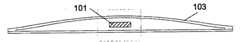
图1表示根据本发明的粘合剂器件的典型表示的形状的模具断面。CT是器件的最大厚度,PT是器件的周缘的厚度。Figure 1 shows a mold section in the shape of a typical representation of an adhesive device according to the invention. CT is the maximum thickness of the device, and PT is the thickness of the periphery of the device.
图2示出嵌入/集成到三维(3D)粘合剂中的微电子系统。缩放框表示图3、图4、图5、图6、图7、图8、图9、图10、图11和图12所示的粘合剂器件的一部分。Figure 2 shows a microelectronic system embedded/integrated into a three-dimensional (3D) adhesive. The zoom box represents a portion of the adhesive device shown in FIGS. 3 , 4 , 5 , 6 , 7 , 8 , 9 , 10 , 11 and 12 .
图3示出完全集成到粘合剂体内的微电子系统(影线框)。Figure 3 shows the microelectronic system fully integrated into the adhesive body (hatched box).
图4示出微电子系统的多个部分可在不同的位置被集成到粘合剂器件内,使得这些部分之间具有适当的机械或电气互连。Figure 4 shows that multiple parts of a microelectronic system can be integrated into an adhesive device at different locations with appropriate mechanical or electrical interconnections between the parts.
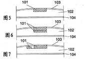
图5示出被施加到粘合剂体内的凹槽中的微电子系统。凹槽是皮肤固定区的远端。微电子系统可任选地是可互换的或可再使用的。Figure 5 shows a microelectronic system applied into a groove within an adhesive body. The groove is the distal end of the skin fixation zone. Microelectronic systems are optionally interchangeable or reusable.
图6示出上部可互换或可再使用并且下部被永久集成到粘合剂体内的微电子系统。Figure 6 shows a microelectronic system where the upper part is interchangeable or reusable and the lower part is permanently integrated into the adhesive body.
图7示出微电子系统的多个部分可在不同的位置位于粘合剂器件内,使得这些部分之间具有适当的机械或电气互连。Figure 7 shows that various parts of a microelectronic system can be located within the adhesive device at different locations with appropriate mechanical or electrical interconnections between the parts.
图8示出被嵌入/施加到粘合剂体的粘合剂侧的凹槽内的微电子系统。Figure 8 shows a microelectronic system embedded/applied into a groove on the adhesive side of the adhesive body.
图9示出具有下部可互换或可再使用并且上部被永久集成到粘合剂体内的微电子系统的器件。Figure 9 shows a device with a microelectronic system whose lower part is interchangeable or reusable and whose upper part is permanently integrated into the adhesive body.
图10示出一些微电子部件(小影线框)在制造过程中被集成到粘合剂体内并且一些微电子部件在以后被施加由此建立必要的机械/电气连接的系统。Figure 10 shows a system in which some microelectronic components (small hatched boxes) are integrated into the adhesive body during the manufacturing process and some microelectronic components are applied later thereby establishing the necessary mechanical/electrical connections.
图11示出被嵌入粘合剂内的微电子系统,该系统从粘合剂体的远端侧和皮肤固定侧均是可施加和可达到的。Figure 11 shows a microelectronic system embedded within an adhesive that is both applicable and accessible from both the distal side of the adhesive body and the skin-fixed side.
图12示出微电子系统由两个部分组装的系统,这两个部分中的一个或每一个可以是可互换的或可再使用的。Figure 12 shows a system in which the microelectronic system is assembled from two parts, one or each of which may be interchangeable or reusable.
在本发明的所有以上结构中,不管上表面上是否存在微电子系统的部件,上表面均保持平滑。可以通过微电子部件的适当构建、封装等实现这一点。In all the above structures of the present invention, the upper surface remains smooth regardless of the presence or absence of components of the microelectronic system on the upper surface. This can be achieved through appropriate construction, packaging, etc. of the microelectronic components.
图8、图9、图10、图11和图12所示的结构特别适于包含例如应具有皮肤接点的电极的元件的微电子系统。The structures shown in Figures 8, 9, 10, 11 and 12 are particularly suitable for microelectronic systems comprising elements such as electrodes which should have skin contacts.
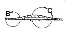
图13~18示出本发明的实施例,这里,天线、中央处理单元、电池和电极被嵌入粘合剂器件内。图13示出器件的二维形状,由A-A指示断面。在图15中,第三维被示为断面A-A。从器件的边缘的圆B在图16中被进一步放大,并且中心的圆C类似地在图17中被放大。图14示出位于粘合剂器件的外部并与微电子系统的中心部分连接的天线的位置。图16更详细地表示被平放嵌入粘合剂内的天线的构建。图1 7表示具有电池、CPU和伸出粘合剂的电极的微电子系统的中心部分的位置。电池和CPU被包封在透明的硅酮橡胶内。最后,图18以三维模式示出粘合剂器件。Figures 13-18 show an embodiment of the invention where the antenna, central processing unit, battery and electrodes are embedded within the adhesive device. Figure 13 shows the two-dimensional shape of the device, with sections indicated by A-A. In Figure 15, the third dimension is shown as section A-A. Circle B from the edge of the device is further enlarged in FIG. 16 , and circle C in the center is similarly enlarged in FIG. 17 . Figure 14 shows the location of the antenna located on the outside of the adhesive device and connected to the central part of the microelectronic system. Figure 16 shows in more detail the construction of the antenna laid flat within the adhesive. Figure 17 shows the location of the central part of the microelectronic system with the battery, CPU and electrodes protruding from the adhesive. The battery and CPU are encapsulated in transparent silicone rubber. Finally, Figure 18 shows the adhesive device in three dimensions.
图19表示在透视分解图中看到的根据本发明的传感器组件的一个实施例。Figure 19 shows an embodiment of a sensor assembly according to the invention seen in a perspective exploded view.
图20表示沿图19中的线XX-XX的断面图中的传感器组件的实施例。FIG. 20 shows an embodiment of a sensor assembly in a cross-sectional view along line XX-XX in FIG. 19 .
图21表示从底端看到的传感器组件的实施例。Figure 21 shows an embodiment of the sensor assembly seen from the bottom.
图22a和图22b表示根据本发明的器件的另一实施例,其中,图22b以放大图表示图22a的一部分。Figures 22a and 22b show another embodiment of a device according to the invention, wherein Figure 22b shows a part of Figure 22a in an enlarged view.
图23表示在透视图中看到的根据本发明的器件的另一实施例。Fig. 23 shows another embodiment of a device according to the invention seen in a perspective view.
图24表示沿图23中的线XXIV-XXIV的断面图中的根据本发明的器件的实施例。FIG. 24 shows an embodiment of a device according to the invention in a cross-sectional view along line XXIV-XXIV in FIG. 23 .
具体实施方式Detailed ways
本发明涉及具有被嵌入由压敏粘合剂制成的粘合剂体中的微电子系统的粘合剂器件。The present invention relates to an adhesive device having a microelectronic system embedded in an adhesive body made of pressure sensitive adhesive.
以下,当限定例如粘合剂体或器件的元件时使用的术语“三维”是指当在断面中观察时轮廓变化相当大的元件。因此,例如,三维粘合剂体将具有最大厚度和最小厚度。根据本发明,最大厚度将为最小厚度的至少两倍。在优选实施例中,粘合剂器件的外边缘或周缘的厚度小于传感器的最厚部分(一般为中心部分)的厚度的一半。Hereinafter, the term "three-dimensional" used when defining an element such as an adhesive body or a device refers to an element whose profile changes considerably when viewed in cross-section. Thus, for example, a three-dimensional adhesive body will have a maximum thickness and a minimum thickness. According to the invention, the maximum thickness will be at least twice the minimum thickness. In a preferred embodiment, the thickness of the outer edge or periphery of the adhesive means is less than half the thickness of the thickest part of the sensor (typically the central part).
与术语“三维”相反,当限定元件时使用的术语“二维”是指具有一般平整的表面的元件。因此,二维粘合剂体的最大厚度小于粘合剂体的最小厚度的两倍。In contrast to the term "three-dimensional", the term "two-dimensional" is used when defining an element to refer to an element having a generally planar surface. Thus, the maximum thickness of the two-dimensional adhesive body is less than twice the minimum thickness of the adhesive body.
如这里使用的那样,关于微电子系统或其部件,术语“嵌入”意味着粘合剂体的压敏粘合剂部分或全部包围微电子系统的全部或一些部件。因此,术语“嵌入”包含系统或部件的所有边被粘合剂体的粘合剂覆盖的情况,并且还包含这样一种情况,即,嵌入的物品不是所有各边都被粘合剂体的粘合剂覆盖,例如,物品被放在粘合剂体中的凹槽或空腔中并且是可从外面到达的。As used herein, the term "embedded" with reference to a microelectronic system or a component thereof means that the pressure sensitive adhesive of the adhesive body partially or fully surrounds all or some components of the microelectronic system. Thus, the term "embedded" includes the situation where all sides of the system or part are covered by the adhesive of the adhesive body, and also includes the situation where the embedded item is not covered by the adhesive body on all sides. Adhesive covers, for example, items are placed in recesses or cavities in the adhesive body and are accessible from the outside.
“嵌入”是用于说明微电子系统位于粘合剂体内的方式的一般术语,而术语“集成”意味着微电子系统或其特定部件在所有各边上都被粘合剂覆盖,并且,当微电子系统仅被部分覆盖时使用术语“施加”。"Embedded" is the general term used to describe the manner in which the microelectronic system is located within the body of the adhesive, while the term "integrated" means that the microelectronic system or specific parts thereof are covered by the adhesive on all sides and, when The term "applied" is used when the microelectronic system is only partially covered.
在所有各边上集成和覆盖还包含这样一种情况,即,集成的部件例如以电气或其它的方式连接到嵌入粘合剂体内的另一部件上。Integrating and covering on all sides also includes the case where an integrated component is connected, for example electrically or otherwise, to another component embedded in an adhesive body.
如这里使用的那样,微电子“感测”系统意味着包含具有能够检测生理或神经条件的元件的换能器的微电子系统。As used herein, a microelectronic "sensing" system means a microelectronic system that includes transducers with elements capable of detecting physiological or neurological conditions.
如这里使用的那样,通孔意味着在粘合剂体的上表面上具有开口并且在粘合剂体的底表面上具有开口的穿过粘合剂体的孔。优选地,通孔在粘合剂体的上表面上具有一个开口并在底表面上具有一个开口。通孔可具有任意适当的形状。As used herein, through hole means a hole through the adhesive body having an opening on the upper surface of the adhesive body and an opening on the bottom surface of the adhesive body. Preferably, the through hole has one opening on the upper surface of the adhesive body and one opening on the bottom surface. The vias may have any suitable shape.
粘合剂器件的“厚度”意味着可在上表面上的特定点到底表面上的点之间画出的最短线或可在底表面上的特定点到上表面上的点之间画出的最短线的长度。The "thickness" of an adhesive device means the shortest line that can be drawn between a specific point on the top surface or between a specific point on the bottom surface and a point on the top surface. The length of the shortest line.
对于本发明,表达“皮肤”被用于表示哺乳动物的外表面。For the purposes of the present invention, the expression "skin" is used to denote the external surface of a mammal.
如上所述,很惊奇地发现,微电子部分被嵌入三维形状的压敏粘合剂体中的无线微电子系统解决已知的传感器器件的问题。As stated above, it has surprisingly been found that a wireless microelectronic system in which the microelectronic parts are embedded in a three-dimensionally shaped body of pressure sensitive adhesive solves the problems of known sensor devices.
由于三维压敏粘合剂的性能,产生对微电子系统的最佳保护。粘合剂向皮肤表面提供密封,并且,由于粘合剂器件顶端的聚合物覆盖层,因此粘合剂器件得到保护免受外面的液体影响。并且,粘合剂保护嵌入的微电子部分免受机械损伤。Due to the properties of the three-dimensional pressure-sensitive adhesive, an optimal protection of microelectronic systems results. The adhesive provides a seal to the skin surface and, due to the polymer cover layer on top of the adhesive device, the adhesive device is protected from external liquids. Also, the adhesive protects the embedded microelectronics from mechanical damage.
根据本发明的粘合剂体由三维形状的压敏粘合剂制成,从粘合剂体的中心到边缘具有变化的厚度,并适当地在粘合剂体最厚的位置具有嵌入粘合剂体内的微电子感测系统。The adhesive body according to the invention is made of a three-dimensionally shaped pressure sensitive adhesive having a varying thickness from the center to the edge of the adhesive body and suitably having an inset bond where the adhesive body is thickest Microelectronic sensing system inside the agent.
具有这种形状并适当地具有斜面边缘的器件提供与皮肤的平滑界面。粘合剂器件将提供柔和的感觉并且将不趋于与衣服和亚麻布发生摩擦。特殊的优点在于,粘合剂器件将不容易由于笨重和边缘的粘性无意中脱落。这对于器件的真正功能是十分重要的。Devices of this shape, suitably with beveled edges, provide a smooth interface with the skin. The adhesive device will provide a soft feel and will not tend to rub against clothing and linens. A particular advantage is that the adhesive device will not easily come off unintentionally due to the bulkiness and stickiness of the edges. This is very important for the true function of the device.
并且,由于粘合剂体具有作为将器件固定到皮肤的手段、微电子系统的保护手段和用于将器件成形为方便的形状的手段的三重功能,因此粘合剂器件的结构十分简便。该结构在三维器件的组装中需要较少的部件和工艺步骤,因此成本不高并且更易于制造。Also, since the adhesive body has a triple function as a means to fix the device to the skin, a means to protect the microelectronic system, and a means to shape the device into a convenient shape, the structure of the adhesive device is very simple. The structure requires fewer parts and process steps in the assembly of the three-dimensional device and is therefore less expensive and easier to manufacture.
根据本发明的一个实施例,三维粘合剂体具有适于粘合到哺乳动物的体表面上的基本上平整的底表面和平滑的上表面。粘合剂器件适当地在体部的中心部分最厚并在体部的边缘最薄。According to one embodiment of the present invention, the three-dimensional adhesive body has a substantially planar bottom surface and a smooth upper surface adapted to adhere to a mammalian body surface. The adhesive means is suitably thickest at the central portion of the body and thinnest at the edges of the body.
优选地,上表面具有平滑的凸形表面,但它原则上可采取任何形式。Preferably, the upper surface has a smooth convex surface, but it may in principle take any form.
粘合剂器件的外边缘或周缘必须被成形为厚度小于传感器的最厚部分(一般为中心部分)的厚度的一半。The outer edge or perimeter of the adhesive device must be formed to a thickness less than half the thickness of the thickest part of the sensor (typically the central part).
因此,在本发明的另一实施例中,粘合剂器件在边缘上的厚度小于粘合剂器件在其最厚位置上的厚度的50%,适当地,边缘上的厚度小于粘合剂器件在其最厚位置上的厚度的25%,优选地,边缘上的厚度小于粘合剂器件在其最厚位置上的厚度的10%,并且,最优选地,边缘上的厚度小于粘合剂器件在其最厚位置上的厚度的5%。Therefore, in another embodiment of the invention, the thickness of the adhesive device at the edge is less than 50% of the thickness of the adhesive device at its thickest point, suitably the thickness at the edge is less than 50% of the thickness of the adhesive device at its thickest point. 25% of the thickness at its thickest point, preferably less than 10% of the thickness of the adhesive device at its thickest point on the edge, and, most preferably, less than the thickness on the edge of the adhesive 5% of the thickness of the device at its thickest point.
粘合剂器件在边缘上的厚度一般小于0.4mm。在一个实施例中,该厚度可以为0.01~0.4mm。适当地,粘合剂器件在边缘上的厚度大于0.05mm,优选为0.05~0.4mm。The thickness of the adhesive device on the edges is generally less than 0.4 mm. In one embodiment, the thickness may be 0.01-0.4 mm. Suitably, the thickness of the adhesive means at the edges is greater than 0.05 mm, preferably 0.05 to 0.4 mm.
一般地,粘合剂器件的厚度为0.5~15mm,更适当地,在一般但不必地在粘合剂体的中心处最厚的情况下为1~5mm。Typically, the thickness of the adhesive device is 0.5 to 15mm, more suitably 1 to 5mm where it is typically but not necessarily thickest in the center of the adhesive body.
适当地,粘合剂器件的底表面和从底表面的周边的任意点到上表面处粘合剂体最厚位置上的点画出的线之间的角度小于60度,优选小于45度,并且最优选小于30度。Suitably, the angle between the bottom surface of the adhesive device and a line drawn from any point on the periphery of the bottom surface to a point on the upper surface where the body of adhesive is thickest is less than 60 degrees, preferably less than 45 degrees, And most preferably less than 30 degrees.
粘合剂体的外边缘可适当被成形为具有或没有瓣或凸起的圆形或椭圆形,或者它可以成形为矩形或三角形以获得尽可能方便和安全的器件。The outer edge of the body of adhesive may suitably be shaped as a circle or oval with or without petals or protrusions, or it may be shaped as a rectangle or a triangle to obtain a device as convenient and safe as possible.
一般地,粘合剂体的周缘将包含粘合剂体的粘合剂。但是,可存在微电子系统或其部件被放在周缘内/或上的实施例,由此,周缘不只包含粘合剂体的粘合剂。Typically, the perimeter of the adhesive body will contain the adhesive of the adhesive body. However, there may be embodiments where the microelectronic system or components thereof are placed within and/or on the perimeter, whereby the perimeter does not contain only the adhesive of the adhesive body.
制成三维粘合剂体的压敏粘合剂适当地为可塑的热塑性或化学固化的压敏粘合剂,该压敏粘合剂具有使得粘合剂器件能够符合身体部位的曲率同时即使在移动条件下也保持其粘合性能的柔性。The pressure sensitive adhesive from which the three-dimensional adhesive body is made is suitably a malleable thermoplastic or chemically cured pressure sensitive adhesive having a curvature which enables the adhesive device to conform to the body part while even in Flexibility to maintain its adhesive properties also under moving conditions.
适当地,制成粘合剂体的压敏粘合剂是基于聚合物的粘合剂,这些聚合物选自诸如苯乙烯嵌段共聚物和氢化苯乙烯嵌段共聚物的嵌段共聚物、无定形聚α烯烃(APAO)、聚丙烯酸、聚乙烯醚、聚氨酯、聚乙烯基乙酸酯、硅酮或水凝胶压敏粘合剂的组。Suitably the pressure sensitive adhesive from which the adhesive body is formed is an adhesive based on polymers selected from block copolymers such as styrenic block copolymers and hydrogenated styrenic block copolymers, Group of amorphous polyalphaolefin (APAO), polyacrylic acid, polyvinyl ether, polyurethane, polyvinyl acetate, silicone or hydrogel pressure sensitive adhesives.
基于这些聚合物的压敏粘合剂是公知的,并且本领域技术人员知道如何制备基于这些聚合物的粘合剂。Pressure-sensitive adhesives based on these polymers are well known and the person skilled in the art knows how to prepare adhesives based on these polymers.
诸如苯乙烯嵌段共聚物和氢化苯乙烯嵌段共聚物的嵌段共聚物可适当地选自苯乙烯/乙烯-丁烯/苯乙烯(SEBS)、苯乙烯/异戊二烯/苯乙烯(SIS)和苯乙烯/乙烯-丙烯/苯乙烯(SEPS)。Block copolymers such as styrene block copolymers and hydrogenated styrene block copolymers may suitably be selected from styrene/ethylene-butylene/styrene (SEBS), styrene/isoprene/styrene ( SIS) and styrene/ethylene-propylene/styrene (SEPS).
粘合剂也可基于PDMS(聚二甲基硅氧烷),并可适当地为PDMS凝胶。The adhesive may also be based on PDMS (polydimethylsiloxane), and may suitably be a PDMS gel.
水凝胶粘合剂也可基于或包含amfifilic聚合物、聚乙烯吡咯烷酮、聚乙烯醇、聚环氧乙烷、明胶、天然树胶和纤维素衍生物或它们的任意组合。Hydrogel adhesives may also be based on or comprise amfifilic polymers, polyvinylpyrrolidone, polyvinyl alcohol, polyethylene oxide, gelatin, natural gums, and cellulose derivatives, or any combination thereof.
压敏粘合剂可根据这些原理并基于在Donatas Satas的手册:Handbook of pressure sensitive adhesive technology,Third edition中列出和公开的聚合物被配制。Pressure sensitive adhesives can be formulated according to these principles and based on the polymers listed and disclosed in Donatas Satas' Handbook: Handbook of pressure sensitive adhesive technology, Third edition.
在本发明的一个特定的实施例中,制成粘合剂体的压敏粘合剂包含水解胶体。包含水解胶体的压敏粘合剂可以是上述类型的压敏粘合剂中的任一种或本领域公知的任何其它压敏粘合剂。In a particular embodiment of the invention, the pressure-sensitive adhesive from which the adhesive body is made comprises hydrocolloids. The pressure sensitive adhesive comprising the hydrocolloid may be any of the types of pressure sensitive adhesives described above or any other pressure sensitive adhesive known in the art.
因此,美国专利No.3339549公开了诸如聚异丁烯的橡胶弹性体和诸如果胶、明胶和羧甲基纤维素的粉状混合物的一种或更多种水溶性或水可膨胀的水解胶体的混合。粘合剂块具有施加到一个表面上的不溶于水的膜。这种类型的成分可在商业上从E.R.Squibb & Sons Inc.按商标“Stomahesive”得到,并被用作气孔周围的皮肤阻挡剂以防止由气孔排出的腐蚀性流体损坏皮肤。Thus, US Patent No. 3339549 discloses the mixing of a rubber elastomer such as polyisobutylene and one or more water-soluble or water-swellable hydrocolloids of a powdered mixture such as pectin, gelatin and carboxymethylcellulose . The adhesive mass has a water-insoluble film applied to one surface. Compositions of this type are commercially available from E.R. Squibb & Sons Inc. under the trademark "Stomahesive" and are used as skin barriers around stomata to prevent damage to the skin by corrosive fluids expelled from the stomata.
在这种类型的粘合剂成分中,聚异丁烯负责提供粘合性能,并且分散的水解胶体粉末吸收流体并使得粘合剂还能够粘合到湿的皮肤上(湿粘性)。这些成分作为用于皮肤溃疡、烧伤和其它的外渗伤口的创伤敷料也得到越来越多的接受。In adhesive compositions of this type, polyisobutylene is responsible for providing the adhesive properties, and the dispersed hydrocolloid powder absorbs fluids and enables the adhesive to adhere also to wet skin (wet tack). These ingredients are also gaining acceptance as wound dressings for skin ulcers, burns and other exuding wounds.
在大量的实施例中,在大量的专利文献中公开的苯乙烯共聚物被加入。In a number of examples, styrene copolymers disclosed in a number of patent documents are incorporated.
因此,Sorensen等人的美国专利No.4231369公开了包含在其中分散了水溶性水解胶体树胶的苯乙烯共聚物和增粘剂的造口术皮肤阻挡剂。Thus, US Patent No. 4,231,369 to Sorensen et al. discloses an ostomy skin barrier comprising a styrene copolymer having dispersed therein a water-soluble hydrocolloid gum and a tackifier.
在美国专利No.4367732中,Poulsen等人公开了包含分散于包含苯乙烯共聚物、碳氢化合物增粘剂和增塑剂的连续相中的水溶性水解胶体、抗氧化剂和油质增充剂的造口术皮肤阻挡剂。In U.S. Patent No. 4,367,732, Poulsen et al. disclose a water-soluble hydrocolloid, an antioxidant, and an oleaginous extender dispersed in a continuous phase comprising a styrene copolymer, a hydrocarbon tackifier, and a plasticizer. ostomy skin barrier.
美国专利No.4551490(Doyle等人)公开了包含5~30%的一种或更多种聚异丁烯、3~20%的双嵌段(diblock)共聚物的含量低于20%的一种或更多种苯乙烯基团或嵌段共聚物、矿物油、一种或更多种水溶性水解胶体树胶和增粘剂的均匀混合物的医疗级压敏粘合剂成分。一种或更多种水可膨胀的粘性增强剂、抗氧化剂和各种其它任选的成分也可被包含于粘合剂成分内。U.S. Patent No. 4,551,490 (Doyle et al.) discloses one or more polyisobutylenes comprising 5 to 30%, 3 to 20% of a diblock copolymer, or A medical grade pressure sensitive adhesive composition of a homogeneous mixture of more styrenic group or block copolymers, mineral oil, one or more water soluble hydrocolloid gums and a tackifier. One or more water-swellable viscosity enhancers, antioxidants, and various other optional ingredients may also be included in the adhesive composition.
美国专利No.5492943公开了包含两种粘弹性粘合剂弹性体、具体而言为高分子量聚异丁烯和苯乙烯嵌段共聚物的混合物的压敏粘合剂成分,该混合物与增塑剂(优选为矿脂)和适当的增粘剂和抗氧化剂一起形成其中分散了诸如羧甲基纤维素钠和果胶的水解胶体的连续相。U.S. Patent No. 5,492,943 discloses pressure sensitive adhesive compositions comprising a blend of two viscoelastic adhesive elastomers, specifically high molecular weight polyisobutylene and a styrene block copolymer, in combination with a plasticizer ( Petrolatum, preferably) together with suitable viscosifiers and antioxidants form a continuous phase in which hydrocolloids such as sodium carboxymethylcellulose and pectin are dispersed.
在美国专利No.4867748中,Samuelsen公开了由与背衬膜组合的水解胶体粘合剂制成的密封垫的几何结构及其处理。In US Patent No. 4,867,748, Samuelsen discloses the geometry of gaskets made of hydrocolloid adhesives combined with backing films and their handling.
在美国专利No.5492943中公开的粘合剂成分被描述为用于将造口术用具粘合到皮肤上的晶片,并且通过包含具有更高含量的双嵌段共聚物的苯乙烯嵌段共聚物与已知的成分不同,从而完全避免使用低分子量聚异丁烯并优选地不包含明胶。The adhesive composition disclosed in U.S. Patent No. 5,492,943 is described as a wafer for bonding ostomy appliances to the skin, and is obtained by including styrene block copolymers with higher content of diblock copolymers The composition differs from known ingredients, thereby avoiding the use of low molecular weight polyisobutylene altogether and preferably containing no gelatin.
包含水解胶体的压敏粘合剂的特征在于具有分散于粘合剂相中的水解胶体的微粒相,它是粘合剂的特别合适的组。包含水解胶体的粘合剂可从皮肤吸收水分,避免皮肤的阻塞,同时维持其对皮肤的粘合性能。并且,包含水解胶体的粘合剂体可具有任意的厚度并仍具有不吸留的性能。水解胶体粘合剂由于热熔性可被处理并且很容易模压为特定的形状。Pressure sensitive adhesives comprising hydrocolloids, which are characterized by having a particulate phase of hydrocolloids dispersed in the adhesive phase, are a particularly suitable group of adhesives. Adhesives containing hydrocolloids absorb moisture from the skin, avoiding skin clogging while maintaining their adhesive properties to the skin. Also, the adhesive body comprising the hydrocolloid can be of any thickness and still have non-occlusive properties. Hydrocolloid adhesives can be processed and easily molded into specific shapes due to their hot melt properties.
这意味着,与易模压性组合的热熔性使得粘合剂体的厚度能够从包含微电子系统的粘合剂器件的边缘逐渐过渡到中心部分,从而提供平滑的没有不连贯的突出的外形。This means that hot melt properties combined with easy moldability enable the thickness of the adhesive body to gradually transition from the edges to the central portion of the adhesive device containing the microelectronic system, thereby providing a smooth profile with no discontinuous protrusions .
以下详细说明用于制造根据本发明的可用于粘合剂体的压敏粘合剂的配方。The formulation for producing the pressure-sensitive adhesive usable for the adhesive body according to the present invention is explained in detail below.
因此,典型的压敏粘合剂成分基于成分的总重量包含10~60wt.%的一种或更多种橡胶状弹性体成分、5~60%的一种或更多种吸收剂粒子、0~50%的增粘剂树脂、0~10%的增塑剂和0~60%的非极性油质增充剂的基本上均匀的混合物。Thus, a typical pressure sensitive adhesive composition comprises 10 to 60 wt.% of one or more rubbery elastomer components, 5 to 60% of one or more absorbent particles, 0 A substantially homogeneous mixture of -50% tackifier resin, 0-10% plasticizer, and 0-60% non-polar oily extender.
橡胶状弹性体基本成分可选自包含物理上交联的弹性体(适当地为包含聚苯乙烯嵌段的嵌段共聚物)、化学交联的天然或合成橡胶状弹性体或橡胶状均聚物的组。The rubbery elastomer base may be selected from the group consisting of physically crosslinked elastomers (suitably block copolymers comprising polystyrene blocks), chemically crosslinked natural or synthetic rubbery elastomers or rubbery homopolymers. group of things.
选自苯乙烯和一种或更多种丁二烯的嵌段共聚物的物理交联的弹性体可以是苯乙烯-丁二烯-苯乙烯嵌段共聚物、苯乙烯-异戊二烯共聚物,并优选是苯乙烯-异戊二烯-苯乙烯和苯乙烯-异戊二烯嵌段共聚物的混合物。Physically cross-linked elastomers selected from block copolymers of styrene and one or more butadiene can be styrene-butadiene-styrene block copolymers, styrene-isoprene copolymers and preferably a mixture of styrene-isoprene-styrene and styrene-isoprene block copolymers.
化学交联的橡胶状弹性体可以是例如丁基橡胶或天然橡胶。The chemically crosslinked rubbery elastomer can be, for example, butyl rubber or natural rubber.
橡胶状均聚物可以是诸如低密度聚乙烯或丙烯的低烯烃的聚合物、优选无规聚丙烯(APP)或聚异丁烯。The rubbery homopolymer may be a polymer of low olefins such as low density polyethylene or propylene, preferably atactic polypropylene (APP) or polyisobutylene.
根据本发明任选使用的增粘树脂优选是氢化增粘剂树脂,并且更优选选自包含环戊二烯、二环戊二烯、α蒎烯或β蒎烯的聚合物和共聚物的组。The tackifying resin optionally used according to the present invention is preferably a hydrogenated tackifying resin and is more preferably selected from the group of polymers and copolymers comprising cyclopentadiene, dicyclopentadiene, alpha-pinene or beta-pinene .
当物理交联的弹性体是苯乙烯-丁二烯-苯乙烯嵌段共聚物或苯乙烯-异戊二烯-苯乙烯嵌段共聚物时,粘合剂适当地包含0~10%的增塑剂(例如,citrofol BII,DOA)。When the physically crosslinked elastomer is a styrene-butadiene-styrene block copolymer or a styrene-isoprene-styrene block copolymer, the adhesive suitably contains 0 to 10% of Plasticizers (eg, citrofol BII, DOA).
膨胀水解胶体粒子优选包含一种或更多种水溶性或水膨胀水解胶体聚合物或树胶。The swollen hydrocolloid particles preferably comprise one or more water-soluble or water-swellable hydrocolloid polymers or gums.
适当的水解胶体包含可以为线性的或交联的合成聚合物,诸如从内酰胺或聚乙烯吡咯烷酮制备的水解胶体。可用于制备合成的水解胶体的其它单体包含丙烯酸盐、异丁烯酸盐和水溶性氨化物。Suitable hydrocolloids comprise synthetic polymers which may be linear or crosslinked, such as hydrocolloids prepared from lactams or polyvinylpyrrolidone. Other monomers that can be used to prepare synthetic hydrocolloids include acrylates, methacrylates, and water-soluble amides.
根据本发明,天然出现或合成制备的其它水解胶体聚合物是可用的。这些材料包含聚乙烯醇、聚氧化烯和诸如聚糖、树胶和改性的纤维素的天然出现或合成地改性的水解胶体。Other hydrocolloid polymers, naturally occurring or synthetically prepared, are useful in accordance with the present invention. These materials include polyvinyl alcohols, polyoxyalkylenes, and naturally occurring or synthetically modified hydrocolloids such as polysaccharides, gums, and modified celluloses.
代表性的聚糖包含淀粉、糖原、半纤维素、戊聚糖、纤维素、果胶、壳聚糖和壳多糖。代表性的树胶包含Arabic、Locust Bean、Guar、Agar、Carrageenan、Xanthan、Karaya、Alginates、Tragacanth、Ghatti和Furcelleran树胶。代表性的改性纤维素包含甲基纤维素、羟丙基甲基纤维素、羧甲基纤维素和羟丙基纤维素。Representative polysaccharides include starch, glycogen, hemicellulose, pentosan, cellulose, pectin, chitosan, and chitin. Representative gums include Arabic, Locust Bean, Guar, Agar, Carrageenan, Xanthan, Karaya, Alginates, Tragacanth, Ghatti, and Furcelleran gums. Representative modified celluloses include methylcellulose, hydroxypropylmethylcellulose, carboxymethylcellulose and hydroxypropylcellulose.
优选的水解胶体包含诸如淀粉、糖原、半纤维素、戊聚糖、明胶、纤维素、改性纤维素、果胶、壳聚糖和壳多糖的聚糖。改性的纤维素包含甲基纤维素、羟丙基甲基纤维素、羧甲基纤维素和羟丙基纤维素。最优选的水解胶体是选自包含聚乙烯醇、粉状果胶、明胶、甲基纤维素、羟丙基甲基纤维素、羧甲基纤维素、羟丙基纤维素和它们的混合物的组的水溶性或膨胀水解胶体。在一个优选实施例中,水解胶体是羧甲基纤维素(CMC)。Preferred hydrocolloids comprise polysaccharides such as starch, glycogen, hemicellulose, pentosan, gelatin, cellulose, modified cellulose, pectin, chitosan and chitin. Modified celluloses include methylcellulose, hydroxypropylmethylcellulose, carboxymethylcellulose and hydroxypropylcellulose. Most preferred hydrocolloids are selected from the group comprising polyvinyl alcohol, powdered pectin, gelatin, methylcellulose, hydroxypropylmethylcellulose, carboxymethylcellulose, hydroxypropylcellulose and mixtures thereof water-soluble or swelling hydrocolloids. In a preferred embodiment, the hydrocolloid is carboxymethylcellulose (CMC).
适当的膨胀胶体是基于交联的聚丙烯酸聚合物的小球形粒子。在美国专利No.4867748、EP 0122344和美国专利申请No.2004065232中可找到这些材料的例子。Suitable swelling colloids are based on small spherical particles of cross-linked polyacrylic acid polymers. Examples of these materials can be found in US Patent No. 4867748, EP 0122344 and US Patent Application No. 2004065232.
有时用于附着粘合剂器件的皮肤可以是潮湿的或者甚至是湿的。在这些情况下,普通的粘合剂不能提供粘合剂器件的足够强和永久的附着。在这些情况下有用的专用粘合剂是水凝胶粘合剂。这些粘合剂基于亲水聚合物和使得能够在粘合剂的完全的皮肤接触表面上平稳摄取水分的增充剂。存在成分范围广泛的这种亲水粘合剂。具有高含量的任选地被部分中和的酸基的亲水聚丙烯酸酯是该粘合剂组中的主要代表。这些粘合剂可以是固有的粘合剂,或者可在干燥条件下用增粘剂和增充剂被配制为希望的粘合剂性能。由于水的摄取将粘合剂转换成更加有塑性的状态,因此,当得到水分时,粘性将根据配方大大增加。替代性的粘合剂基于诸如聚乙烯吡咯烷酮、聚乙烯醇、聚环氧乙烷等的聚合物。两性聚合物或可通过基团聚合化学交联的聚合物可被添加以提高粘合剂的粘性,并且一般优选诸如聚乙二醇、聚丙二醇和丙三醇的增充剂。Sometimes the skin used to attach the adhesive device can be damp or even wet. In these cases, common adhesives do not provide a sufficiently strong and permanent attachment of the adhesive device. A specialized adhesive useful in these cases is a hydrogel adhesive. These adhesives are based on hydrophilic polymers and extenders that enable smooth water uptake on the complete skin-contacting surface of the adhesive. Such hydrophilic binders exist in a wide range of compositions. Hydrophilic polyacrylates with a high content of optionally partially neutralized acid groups are the main representatives of this group of adhesives. These adhesives may be inherent adhesives, or may be formulated dry with tackifiers and extenders to provide the desired adhesive properties. Since water uptake converts the adhesive into a more plastic state, the tack will increase greatly depending on the formulation when moisture is available. Alternative adhesives are based on polymers such as polyvinylpyrrolidone, polyvinyl alcohol, polyethylene oxide, and the like. Amphoteric polymers or polymers that can be chemically crosslinked by radical polymerization can be added to increase the tack of the adhesive, and extenders such as polyethylene glycol, polypropylene glycol, and glycerol are generally preferred.
基于聚二甲基硅氧烷(PDMS)的粘合剂成分从19世纪70年代为人们所认识。最近,新的子类的基于PDMS的压敏粘合剂即软硅酮粘合剂已被开发。软硅酮粘合剂(SSA)是基于交联的硅酮弹性体结构的两部分的不溶解粘合剂。交联是具有乙烯基的聚二甲基硅氧烷和氢功能硅氧烷之间的加成反应的结果。固化反应被铂络合物催化并可在室温下发生,或者可在高温(80℃~145℃)下被加速使得不形成副产物。这些粘合剂的特征在于较软并且符合皮肤的表面结构,由此迅速实现皮肤的湿润。由于粘性成分最少,因此材料不流动,并且当施加变形压力时仅出现较小的能量耗散。结果是迅速的剥离,这种剥离在较低的剥离力或剪切力下发生,这对于一些情况可能是有利的。Adhesive compositions based on polydimethylsiloxane (PDMS) have been known since the 1970s. Recently, a new subclass of PDMS-based pressure-sensitive adhesives, soft silicone adhesives, has been developed. Soft silicone adhesives (SSA) are two-part insoluble adhesives based on a cross-linked silicone elastomer structure. Crosslinking is the result of an addition reaction between polydimethylsiloxanes with vinyl groups and hydrofunctional siloxanes. The curing reaction is catalyzed by platinum complexes and can occur at room temperature, or can be accelerated at high temperatures (80°C to 145°C) so that by-products are not formed. These adhesives are characterized by being relatively soft and conforming to the surface structure of the skin, thereby quickly achieving moisturization of the skin. Due to the minimal viscous component, the material does not flow and only a small energy dissipation occurs when deformation pressure is applied. The result is rapid peeling, which occurs at lower peel or shear forces, which may be advantageous in some cases.
由于基于PDMS的压敏粘合剂可用自来水清洗并可被重新施加到皮肤上,因此,除了是优异的皮肤粘合剂以外,它们还具有可再使用的性能。Since PDMS-based pressure-sensitive adhesives can be washed with running water and reapplied to the skin, besides being excellent skin adhesives, they also have reusable properties.
用于制作本发明的粘合剂体的压敏粘合剂也可以是常被描述为粘性凝胶的PDMS凝胶。这些市售系统的例子是来自Dow CorningHealth Care US的Dow Corning 7-9800A&B或来自Wacker-ChemieGmbH,Burghausen,Germany的SilGel 612和来自NuSil Technology,Carpinteria,USA的MED-6340。The pressure sensitive adhesive used to make the adhesive body of the present invention may also be a PDMS gel, often described as a tacky gel. Examples of these commercially available systems are Dow Corning 7-9800A & B from Dow Corning Health Care US or SilGel 612 from Wacker-Chemie GmbH, Burghausen, Germany and MED-6340 from NuSil Technology, Carpinteria, USA.
上述压敏粘合剂可以以无泡沫型或以泡沫型被使用。当在制造过程中气泡被引入压敏粘合剂中时,重量轻的胞状结构被制造。这种压敏粘合剂比无泡沫型更柔软。(参见美国专利No.6326524和美国专利申请No.2004065232)。The above-mentioned pressure-sensitive adhesive may be used in a non-foamed type or in a foamed type. When air bubbles are introduced into the pressure-sensitive adhesive during the manufacturing process, a lightweight cell-like structure is created. This pressure sensitive adhesive is softer than the non-foam type. (See US Patent No. 6326524 and US Patent Application No. 2004065232).
一般地,本发明的粘合剂体具有希望的弹性、粘性、水分传送和/或吸收性能以及较高的舒适性和柔性。柔性提供能够符合身体部位的曲率同时即使在移动条件下也保持其粘合性能的合成。室温下的较高的初始粘性便于粘合剂器件的施加。In general, the adhesive bodies of the present invention have desirable elasticity, tack, moisture transport and/or absorption properties as well as high comfort and flexibility. Flex provides a composition that conforms to the curvature of the body part while maintaining its adhesive properties even under moving conditions. The higher initial tack at room temperature facilitates the application of the adhesive device.
本发明的粘合剂在上表面上具有任何性质的一个或更多个覆盖层、优选仅仅一个覆盖层,以防止对于亚麻布、衣服和其它环境的粘合。The adhesive of the present invention has one or more cover layers of any nature, preferably only one cover layer, on the upper surface to prevent adhesion to linen, clothing and other environments.
作为覆盖材料,优选使用热塑性聚合物膜形式的膜或编织或非编织层。覆盖层优选由弹性材料制成。覆盖层适当地能够传送水分,并可例如由聚合物和聚合物的任意叠层制成,这些聚合物诸如:例如聚乙烯、聚丙烯或聚丁烯的聚烯烃类、诸如尼龙的聚酰胺、聚氨酯、聚乙酸乙烯酯、聚氯乙烯、氟化聚乙烯化合物、聚偏二氯乙烯、聚乙烯醇、乙烯醋酸乙烯酯(ethylene vinyl acetate)、醋酸纤维素或其它的热塑性聚糖、诸如PEBAX的聚醚嵌段氨化物、诸如苯乙烯-异戊二烯-苯乙烯嵌段共聚物或乙烯丙烯酸盐嵌段共聚物的嵌段共聚物、诸如聚对苯二甲酸乙二醇酯(PET)或其衍生物的聚酯。覆盖层可适当地是由聚氨酯、聚乙烯或聚乙酸乙烯酯制成的薄泡沫层等。As covering material, preference is given to using films in the form of thermoplastic polymer films or woven or non-woven layers. The covering layer is preferably made of elastic material. The cover layer is suitably capable of transmitting moisture and may for example be made of polymers and any laminates of polymers such as: polyolefins such as polyethylene, polypropylene or polybutylene, polyamides such as nylon, Polyurethane, polyvinyl acetate, polyvinyl chloride, fluorinated polyvinyl compounds, polyvinylidene chloride, polyvinyl alcohol, ethylene vinyl acetate, cellulose acetate or other thermoplastic polysaccharides, such as PEBAX Polyether block amides, block copolymers such as styrene-isoprene-styrene block copolymers or ethylene acrylate block copolymers, such as polyethylene terephthalate (PET) or Its derivatives are polyesters. The covering layer may suitably be a thin foam layer or the like made of polyurethane, polyethylene or polyvinyl acetate.
覆盖层或膜保护集成的/嵌入的微电子部件以及粘合剂体免受环境影响。The cover layer or film protects the integrated/embedded microelectronic component and the adhesive body from the environment.
在本发明的一个特定的实施例中,天线可通过导电墨水或印刷金属被直接印刷到覆盖层上。In a particular embodiment of the invention, the antenna can be printed directly onto the cover layer by means of conductive ink or printed metal.
在施加到皮肤上之前,为了保证保持粘合剂的性能并且为了使得粘合剂表面在使用前才被铺开,保护性释放衬套覆盖压敏粘合剂体的皮肤接触侧。释放衬套适当地为硅化或氟化释放衬套,诸如硅化或氟化牛皮纸、聚乙烯、聚丙烯或聚对苯二甲酸乙二醇酯膜。适当地,释放衬套是硅化聚乙烯膜,诸如来自公司Huhtamaki的中密度聚乙烯。Prior to application to the skin, a protective release liner covers the skin contacting side of the pressure sensitive adhesive body to ensure that the properties of the adhesive are maintained and to allow the adhesive surface to be spread just prior to use. The release liner is suitably a siliconized or fluorinated release liner, such as siliconized or fluorinated kraft paper, polyethylene, polypropylene or polyethylene terephthalate film. Suitably the release liner is a siliconized polyethylene film, such as medium density polyethylene from the company Huhtamaki.
微电子系统包含大量的部件,这些部件可被组装到一个任选地封装的单元中,该单元被加入本发明的粘合剂器件内。微电子感测系统的部件也可以是位于粘合剂器件中的不同位置中的单个的任选地封装的部件的组件。本发明的该实施例包含粘合剂器件使微电子器件的所有的各单个部件位于不同位置的情况以及部件中的一个或更多个位于与位于同一位置的其它部件的位置不同的位置的情况。Microelectronic systems comprise a large number of components that can be assembled into an optionally encapsulated unit that is incorporated into the adhesive device of the present invention. The components of the microelectronic sensing system may also be an assembly of individual, optionally packaged components located in different locations within the adhesive device. This embodiment of the invention encompasses the case where the adhesive means has all of the individual components of the microelectronic device in different positions and the case where one or more of the components are in a different position than the other components that are co-located .
当微电子器件的部件位于粘合剂器件中的不同位置时,粘合剂器件还在集成到粘合剂体内的部件之间具有必要的机械或电气连接。The adhesive device also has the necessary mechanical or electrical connections between the components integrated into the adhesive body when the components of the microelectronic device are located at different locations in the adhesive device.
因此,根据本发明的一个实施例,整个微电子系统被集成到粘合剂体内,并在所有各边被粘合剂体完全覆盖。Thus, according to one embodiment of the invention, the entire microelectronic system is integrated into the adhesive body and is completely covered by the adhesive body on all sides.
根据本发明的另一实施例,整个微电子系统被包含于设置在面对覆盖层的粘合剂体的上表面中的凹槽内。According to another embodiment of the invention, the entire microelectronic system is contained within a recess provided in the upper surface of the adhesive body facing the cover layer.
根据本发明的另一实施例,整个微电子系统被包含于设置在粘合剂体的粘合剂底表面中的凹槽中。在本发明的另一实施例中,微电子系统被包含于粘合剂体中的通孔中并且从面对覆盖层的上表面以及从粘合剂底表面均可到达。According to another embodiment of the invention, the entire microelectronic system is contained in recesses provided in the adhesive bottom surface of the adhesive body. In another embodiment of the invention, the microelectronics are contained in through-holes in the adhesive body and are accessible both from the upper surface facing the cover layer and from the adhesive bottom surface.
在本发明的替代性的实施例中,微电子系统的一个或更多个部件被集成到粘合剂体内,并且在所有各边被粘合剂体覆盖,并且,微电子系统的其它部件位于粘合剂体的其它位置,微电子感测系统的部件相互具有必要的机械和电气连接。In an alternative embodiment of the invention, one or more components of the microelectronic system are integrated into the adhesive body and are covered on all sides by the adhesive body, and the other components of the microelectronic system are located Elsewhere in the adhesive body, the components of the microelectronic sensing system have the necessary mechanical and electrical connections to each other.
根据本发明的上述实施例,微电子系统的一个或更多个部件可被集成到粘合剂体内并在所有各边被粘合剂体覆盖,并且微电子系统的其余部分被包含于设置在面对覆盖层的粘合剂体的上表面中的一个或更多个凹槽(适当为一个凹槽)内。According to the above-described embodiments of the present invention, one or more components of the microelectronic system may be integrated into the adhesive body and covered on all sides by the adhesive body, and the rest of the microelectronic system is contained in a One or more grooves, suitably one groove, in the upper surface of the adhesive body facing the cover layer.
作为替代方案,微电子系统的一个或更多个部件被集成到粘合剂体内并在所有各边被粘合剂体覆盖,并且微电子系统的其余部分被包含于设置在粘合剂体的粘合剂底表面中的一个或更多个凹槽(适当地为一个凹槽)中。Alternatively, one or more components of the microelectronic system are integrated into the adhesive body and covered on all sides by the adhesive body, and the rest of the microelectronic system is contained in a One or more grooves, suitably a groove, in the bottom surface of the adhesive.
在另一替代性实施例中,微电子系统的一个或更多个部件被集成到粘合剂体内并被粘合剂体覆盖,并且微电子系统的其余部分被包含于粘合剂体中的一个或更多个通孔(适当地为一个通孔)中,并且从面对覆盖层的上表面和粘合剂底表面均可到达。In another alternative embodiment, one or more components of the microelectronic system are integrated into and covered by the adhesive body, and the remainder of the microelectronic system is contained within the adhesive body. One or more through holes, suitably a through hole, and are accessible from both the upper surface facing the cover layer and the bottom surface of the adhesive.
在另一替代性实施例中,微电子系统的一个或更多个部件被集成到粘合剂体内并被粘合剂体覆盖,同时,微电子系统的其它部件被包含于粘合剂体中的一个或更多个通孔(适当地为一个通孔)中,并且从面对覆盖层的上表面和粘合剂底表面均可到达,并且,微电子系统的其余部分被包含于设置在粘合剂体的上和/或底表面中的一个或更多个凹槽(适当地为一个凹槽)中。In another alternative embodiment, one or more components of the microelectronic system are integrated into and covered by the adhesive body while other components of the microelectronic system are contained within the adhesive body one or more through holes (suitably a through hole), and both are accessible from the upper surface facing the cover layer and the bottom surface of the adhesive, and the rest of the microelectronic system is contained in the In one or more grooves, suitably a groove, in the upper and/or bottom surface of the adhesive body.
在另一替代性实施例中,微电子系统的一个或更多个部件被包含于粘合剂体中的一个或更多个通孔(适当地为一个通孔)中,并且从面对覆盖层的上表面或粘合剂底表面均可到达,并且,微电子系统的其余部分被包含于设置在粘合剂体的上和/或底表面中的一个或更多个凹槽(适当地为一个凹槽)中。In another alternative embodiment, one or more components of the microelectronic system are contained in one or more through-holes (suitably a through-hole) in the adhesive body and are covered from face to face. Both the upper surface of the layer or the bottom surface of the adhesive are accessible, and the rest of the microelectronic system is contained in one or more grooves (suitably located in the upper and/or bottom surface of the adhesive body). for a groove).
在另一适当的实施例中,微电子系统的一个或更多个部件被包含于粘合剂体的上表面中的一个或更多个凹槽中(适当地在一个凹槽中),并且微电子系统的其余部分被包含于粘合剂体的底表面中的一个或更多个凹槽(适当地为一个凹槽)中。In another suitable embodiment, one or more components of the microelectronic system are contained in one or more grooves (suitably in a groove) in the upper surface of the adhesive body, and The remainder of the microelectronic system is contained in one or more grooves, suitably one groove, in the bottom surface of the adhesive body.
在微电子系统或其部件被放在粘合剂体的上表面中的情况下,它们适当地遵循轮廓与上表面一起形成,或者被成形为配合粘合剂体的上表面。可以通过适当的部件封装实现这一点。Where microelectronic systems or components thereof are placed in the upper surface of the adhesive body, they are suitably contoured with, or shaped to fit, the upper surface of the adhesive body. This can be achieved through appropriate component packaging.
如上所述,微电子系统的各单个部件、各单个部件的多个组或所有部件可在它们被嵌入粘合剂体之前被封装。当希望保护部件免受环境影响和/或保护环境免受部件影响的附加保护时,例如,当已存在于粘合剂体中或在制造过程中导致集成到粘合剂体中时,选择封装。微电子系统的封装的部件通过必要的电气和/或机械连接相互连接。As mentioned above, individual components, groups of individual components, or all components of the microelectronic system may be encapsulated before they are embedded in the adhesive body. Encapsulation is chosen when protection of the component from the environment and/or additional protection of the environment from the component is desired, for example when it is already present in the adhesive body or has resulted in integration into the adhesive body during the manufacturing process . The packaged components of the microelectronic system are interconnected by the necessary electrical and/or mechanical connections.
在一些情况下,由于粘合剂中的湿气和/或渗出物将引起腐蚀,因此要求保护微电子系统或其部件免受其影响,或者出于其它的原因需要屏蔽外部影响。在这些情况下,微电子系统或其部件被封装。In some cases, it is desirable to protect the microelectronic system or its components from corrosion since moisture and/or exudates in the adhesive will cause corrosion, or to shield it from external influences for other reasons. In these cases, microelectronic systems or components thereof are packaged.
大量的封装技术是已知的,并且包括涂敷、热熔封装、陶瓷封装和玻璃封装。用于封装电气部件的其它方法是本领域公知的。A number of encapsulation techniques are known and include coating, hot melt encapsulation, ceramic encapsulation and glass encapsulation. Other methods for packaging electrical components are known in the art.
微电子系统或其部件被适当地封装到聚合物膜、聚合物箔或聚合物涂层中,或者,微电子系统或其部件被模压到聚合物材料中或被封装到玻璃或陶瓷材料中。The microelectronic system or its components are suitably encapsulated in a polymer film, polymer foil or polymer coating, or the microelectronic system or its components are molded into a polymer material or encapsulated in a glass or ceramic material.
通过涂敷进行的封装一般包含用诸如环氧树脂、PDMS(硅酮)、丙烯酸盐、聚氨酯或UV硬化树脂的材料涂敷部件。Encapsulation by coating generally involves coating the part with a material such as epoxy, PDMS (silicone), acrylate, polyurethane or UV hardening resin.
由于硅酮表面容易从粘合剂体的粘合剂被释放,因此,当微电子部件要被放入粘合剂体中的通孔或凹槽中时,或者在希望使得容易去除或更换封装的微电子部件的情况下,特别优选诸如PDMS的硅酮中的封装。可很容易地从粘合剂释放的其它材料也可用于封装。Since the silicone surface is easily released from the adhesive of the adhesive body, it is useful when microelectronic components are to be placed into through holes or grooves in the adhesive body, or when it is desired to allow easy removal or replacement of the package. In the case of microelectronic components, encapsulation in silicone such as PDMS is particularly preferred. Other materials that are readily releasable from the adhesive can also be used for encapsulation.
热熔性封装一般包含通过注模在热塑性材料中加入微电子系统或其部件。使用的热塑性材料可选自苯乙烯嵌段共聚物、聚氨酯、ABS(丙烯腈-丁二烯-苯乙烯共聚物)、SAN(苯乙烯-丙烯腈共聚物)、聚氯乙烯、PDMS、POM(聚氧化甲烯)、聚苯乙烯、聚酯、聚丙烯酸盐、聚烯烃,例如聚乙烯或聚丙烯。Hot melt encapsulation generally involves incorporating microelectronic systems or components thereof in thermoplastic materials by injection molding. The thermoplastic material used can be selected from styrenic block copolymer, polyurethane, ABS (acrylonitrile-butadiene-styrene copolymer), SAN (styrene-acrylonitrile copolymer), polyvinyl chloride, PDMS, POM ( polyoxymethylene), polystyrene, polyester, polyacrylate, polyolefins such as polyethylene or polypropylene.
微电子系统的部件需要互连。各系统可包含需要在机械上或电学上被组装的一个或更多个离散的部件。可通过PCB(印刷电路板)、弹簧锁、薄的柔性PCB、胶水等建立机械或电学连接。The components of a microelectronic system need to be interconnected. Each system may contain one or more discrete components that need to be assembled mechanically or electrically. The mechanical or electrical connection can be established via PCB (Printed Circuit Board), snap locks, thin flex PCB, glue, etc.
在上述的一个实施例中,微电子感测系统的所有部分都在制造中被集成到粘合剂体内,这意味着具有微电子系统的粘合剂器件具有一次性的性质。In one embodiment described above, all parts of the microelectronic sensing system are integrated into the adhesive body during manufacture, which means that the adhesive device with the microelectronic system has a disposable nature.
根据本发明的粘合剂器件也可以以这种方式被构建,即,微电子系统的部件可在粘合剂器件的寿命期间被更换,或者可在新的粘合剂器件中被重新使用。The adhesive device according to the invention can also be constructed in such a way that components of the microelectronic system can be replaced during the lifetime of the adhesive device, or can be reused in a new adhesive device.
微电子系统的某些部件在制造中被集成到粘合剂体内,而剩余的部件在之后、紧挨着附着到皮肤上之前或附着到皮肤上之后被施加到本发明的粘合剂器件上。在粘合剂体的制造之后施加到粘合剂体上的部件一般是可互换的或可再用的。Certain components of the microelectronic system are integrated into the adhesive body during manufacture, while the remaining components are applied to the adhesive device of the present invention afterward, immediately before or after attachment to the skin . Components applied to the adhesive body after manufacture of the adhesive body are generally interchangeable or reusable.
可被更换的部件例如为能源,例如电池。A replaceable component is, for example, an energy source, such as a battery.
在本发明的特定实施例中,整个微电子系统是可互换的或可再用的,并且可在紧挨着附着之前或在被施加到皮肤上之后被施加到粘合剂器件上。In certain embodiments of the invention, the entire microelectronic system is interchangeable or reusable and can be applied to the adhesive device immediately before attachment or after application to the skin.
适当地,可互换部件或可再用部件如上面所述的那样被封装并形成配合粘合剂体中的凹槽或孔的封装件。Suitably, the interchangeable or reusable part is encapsulated as described above and forms an enclosure that fits into a recess or hole in the body of adhesive.
在可互换或可再用部件的情况下,它们必须具有一些类型的使用中对粘合剂体的安全附着手段。这些附着手段可由粘合剂提供,例如,由已存在于凹痕中的粘合剂体的压敏粘合剂提供,该凹痕是粘合剂体中的孔的空腔。In the case of interchangeable or reusable parts, they must have some type of secure attachment means to the adhesive body in use. These means of attachment may be provided by an adhesive, for example by a pressure sensitive adhesive of the adhesive body already present in the indentation, which is the cavity of the hole in the adhesive body.
在这种情况下,优选封装材料是不太强地粘合到粘合剂体的粘合剂上的材料,见上文。In this case, it is preferred that the encapsulating material is a material which does not adhere too strongly to the adhesive of the adhesive body, see above.
作为替代方案,封装的可互换或可再用部件的封装件通过对粘合剂体的机械耦合被附着到粘合剂体上。上述的包含可更换或可再用部件的封装的封装件可由此通过弹簧锁机构被配入粘合剂体中。Alternatively, the package of packaged interchangeable or reusable components is attached to the adhesive body by mechanical coupling to the adhesive body. A packaged package as described above containing replaceable or reusable components may thus be fitted into the adhesive body by a snap-lock mechanism.
封装用作微电子系统或其部件的外壳,并适当地由注模的聚合物材料形成,但大致上可以为任何材料和任何结构。The encapsulation serves as an enclosure for the microelectronic system or components thereof, and is suitably formed of injection molded polymer material, but may be of generally any material and of any construction.
封装的微电子部件的封装件可具有任意适当的形状,适当地为配合粘合剂体中的凹槽或通孔的三维形状。在一个实施例中,封装的电子部件将具有具有圆端的棒状胶囊的形状。The package of the encapsulated microelectronic component may have any suitable shape, suitably a three-dimensional shape that fits a groove or via in the adhesive body. In one embodiment, the packaged electronic component will have the shape of a stick capsule with rounded ends.
如上所述,本发明使用用于获取生理数据的侵入式以及非侵入式技术。在非侵入式测量的情况下,一个或更多个金属电极可被用于皮肤接点。但是,任何导电材料均可被用于皮肤接点,诸如导电的聚合物、导电的水凝胶和电解质。在侵入式测量的情况下,常规的针或显微针可被使用。当前这种侵入式技术已是公知的例如用于测量氧或血糖的技术。As noted above, the present invention uses invasive as well as non-invasive techniques for acquiring physiological data. In the case of non-invasive measurements, one or more metal electrodes can be used for the skin contact. However, any conductive material can be used for the skin contact, such as conductive polymers, conductive hydrogels, and electrolytes. In the case of invasive measurements, conventional needles or microneedles can be used. Such invasive techniques are currently known eg for measuring oxygen or blood sugar.
通过组合详细说明的部件,所有类别的微电子感测系统均可被设计和加入到本发明的粘合剂器件中。适于嵌入粘合剂器件中的系统的例子是适于测量生物传感器信号、EKG、EMG、EEG、血糖、脉搏、血压、pH值和氧的系统。By combining the components specified, all classes of microelectronic sensing systems can be designed and incorporated into the adhesive devices of the present invention. Examples of systems suitable for embedding in adhesive devices are systems suitable for measuring biosensor signals, EKG, EMG, EEG, blood glucose, pulse, blood pressure, pH and oxygen.
加入本发明的粘合剂器件中的微电子系统一般需要以下的部件:通信部件、CPU(中央处理单元)、电源、存储部件、换能器部件、互连,并任选地包含致动器部件。Microelectronic systems incorporated into adhesive devices of the present invention generally require the following components: communication components, CPU (Central Processing Unit), power supply, storage components, transducer components, interconnects, and optionally include actuators part.
CPU(中央处理单元)控制微电子系统的部件并与它们通信。CPU操纵应用软件、数据决策(诸如数据信号处理)、A/D转换、DSP(数字信号处理)、路由选择、定时、电力管理、休眠功能、中断的执行。The CPU (Central Processing Unit) controls and communicates with the components of the microelectronic system. The CPU handles execution of application software, data decision making (such as data signal processing), A/D conversion, DSP (digital signal processing), routing, timing, power management, sleep functions, interrupts.
CPU是微电子系统的控制其它部件并进行适当的数据分析的部件。一般地,需要的速度和数据分析越多,则需要的电力越多。因此,为了节省电力,休眠功能常被使用。在某些时间,或者如果某件事件发生(由功率非常低的监视子系统触发),那么CPU被唤醒,进行必要的计算,与相关的部件通信并返回休眠模式。根据本发明,可根据需要使用从非常基本的CPU到功能强大的微控制器。The CPU is the part of the microelectronic system that controls the other parts and performs appropriate data analysis. In general, the more speed and data analysis required, the more power is required. Therefore, in order to save power, the sleep function is often used. At certain times, or if some event occurs (triggered by a very low power monitoring subsystem), the CPU wakes up, performs the necessary calculations, communicates with the relevant components and returns to sleep mode. According to the invention, everything from a very basic CPU to a powerful microcontroller can be used as required.
通信部件控制送往和来自微电子系统的所有通信。适当地,微电子系统是使得能够与离开粘合剂器件某一距离的接收器单元无线通信的系统。但是,本发明不限于诸如RF无线通信的无线通信。其它的通信手段可以是音频或光学通信手段。部件包含必要的用于实现这种无线通信的电子部件,还包含天线以及必要的硬件和软件。The communications component controls all communications to and from the microelectronic system. Suitably, the microelectronic system is a system enabling wireless communication with a receiver unit at a distance from the adhesive device. However, the present invention is not limited to wireless communications such as RF wireless communications. Other means of communication may be audio or optical means of communication. The components contain the electronics necessary to enable this wireless communication, as well as the antenna and the necessary hardware and software.
天线可根据频率、功率和信号形式采取不同的形状和形式。一些天线用于在几厘米的范围上传送信息,另一些天线的范围为几米。天线的例子是:环绕小铁氧体磁芯(例如,直径小于4mm)的线圈、具有多圈的扁平线圈(直径一般为10mm或更大)、诸如单极或双极天线的单和双导线射电天线和集成到粘合剂中的天线。Antennas can take different shapes and forms depending on frequency, power and signal form. Some antennas are used to transmit information over a range of a few centimeters, others have a range of a few meters. Examples of antennas are: coils around small ferrite cores (e.g. less than 4mm in diameter), flat coils with multiple turns (typically 10mm in diameter or more), single and dual conductors such as monopole or dipole antennas Radio antennas and antennas integrated into adhesives.
只具有几圈和例如50mm的大直径的天线可被层叠并被集成到粘合剂体中或被印刷到或直接放在粘合剂器件的覆盖层上。天线一般由诸如铜或铝的金属制成,但也可以是导电墨水。Antennas with only a few turns and a large diameter of eg 50 mm can be laminated and integrated into the adhesive body or printed or placed directly on the cover layer of the adhesive device. Antennas are typically made of metals such as copper or aluminum, but can also be conductive ink.
电源包含功率调节电子部件、再充电电子部件和一般为内部或可互换电池的能源。但是,其它的为微电子系统得到电力的手段可被提出,诸如动能转换、燃料电池、同位素辐射、太阳能电池,或者通过射频(RF)链路。并且,天线可被用于将能量加载到微电子系统中。The power supply contains power conditioning electronics, recharging electronics, and an energy source, typically an internal or interchangeable battery. However, other means of obtaining power for microelectronic systems can be proposed, such as kinetic energy conversion, fuel cells, isotopic radiation, solar cells, or via radio frequency (RF) links. Also, the antenna can be used to load energy into the microelectronic system.
优选地,电源是电池,并且可以为一次性使用或可以为可充电的。Preferably, the power source is a battery and may be single use or may be rechargeable.
存储部件用于存储嵌入的系统软件和/或存储在器件的操作中获取的数据。存储部件可以是CPU的一部分、其自身的部件或可被去除和更换的诸如FLASH RAM的可互换存储器。The memory component is used to store embedded system software and/or store data acquired during operation of the device. The storage unit can be part of the CPU, its own unit or an interchangeable memory such as FLASH RAM that can be removed and replaced.
换能器部件是被设计为将能量从一种形式转换成另一种形式的部件。换能器一般为但不限于微电子系统的传感器或感测部分。换能器可由此能够转换例如物理输入,并且换能器将一般但不必将该能量转换成要被CPU等解释的电气形式。A transducer component is a component designed to convert energy from one form to another. A transducer is generally, but not limited to, a sensor or sensing portion of a microelectronic system. The transducer may thus be able to convert eg a physical input, and the transducer will typically but not necessarily convert this energy into an electrical form to be interpreted by a CPU or the like.
换能器可转换的物理输入的例子是加速度、化学品/气体、流量、湿度、惯性、电容、导电率、传导率、电流、阻抗、电感、pH值、电阻、电阻率、电压、光检测、光、磁性、压力、角度、线性位置、速度、温度、声音和机械力。Examples of physical inputs that a transducer can transduce are acceleration, chemical/gas, flow, humidity, inertia, capacitance, conductivity, conductivity, current, impedance, inductance, pH, resistance, resistivity, voltage, light detection , light, magnetism, pressure, angle, linear position, velocity, temperature, sound and mechanical force.
换能器的切实代表是检测部件。检测部件一般选自电极(极性、双极)、压力传感器、具有电极的针、加速计、光检测器、麦克风、离子敏感场效应晶体管(ISFET)、NTC(负温度系数)电阻器、带隙检测器、离子膜、酶反应器或电容器。A tangible representation of the transducer is the detection component. The detection components are generally selected from electrodes (polar, bipolar), pressure sensors, needles with electrodes, accelerometers, light detectors, microphones, ion sensitive field effect transistors (ISFETs), NTC (negative temperature coefficient) resistors, band Gap detectors, ionic membranes, enzyme reactors or capacitors.
在本发明的一个实施例中,换能器包含用于非侵入检测的检测器,诸如电极。In one embodiment of the invention, the transducer contains detectors, such as electrodes, for non-invasive detection.
在本发明的另一实施例中,换能器包含侵入式检测器,诸如包含电极的针。In another embodiment of the invention, the transducer comprises an intrusive detector, such as a needle comprising electrodes.
致动器与换能器相反。它以与换能器基本上相同的方式但以相反的次序将能量从一种形式转换成另一种形式。通常它将电信号转换成物理信号。致动器的切实代表是例如电极(例如用于神经系统或神经刺激)、泵、注射针、发光二极管(LED)或另一光源、扬声器、电流发生器或化学分析仪。致动器的可能的用途在某些事件中由CPU决定,以激活微电子系统中的警报,诸如扬声器或LED,或者指示电池电量低。Actuators are the opposite of transducers. It converts energy from one form to another in essentially the same way as a transducer, but in the reverse order. Usually it converts electrical signals into physical signals. Concrete representatives of actuators are eg electrodes (eg for nervous system or nerve stimulation), pumps, injection needles, light emitting diodes (LEDs) or another light source, loudspeakers, current generators or chemical analyzers. Possible uses of the actuator are determined by the CPU in certain events, to activate an alarm in the microelectronic system, such as a speaker or an LED, or to indicate a low battery.
因此,致动器可被用作系统中的对从诸如警报(可视的和可听的)、注射泵、阀等的换能器部件获得的输入做出反应的部件。它可以是一次使用、多次使用或连续使用的致动器。Thus, actuators may be used as components in the system that react to inputs obtained from transducer components such as alarms (visual and audible), syringe pumps, valves, and the like. It can be a single use, multiple use or continuous use actuator.
许多感测系统仅是传送关于哺乳动物的身体条件的信息的情报系统,并且在这种情况下不需要致动器。Many sensing systems are simply intelligence systems that convey information about the physical condition of the mammal, and in this case no actuators are required.
微电子系统将在用于给定应用的器件中可能仅需要部件中的一些的意义上被模块化构建。一些应用将利用很少的部件,并且一些应用可使用所有的部件。这些部件可被配入相同的物理ASIC(专用集成电路)、电气系统或子系统,诸如但不限于PCB(印刷电路板)、柔性PCB、厚膜、薄膜或陶瓷技术,或者,系统或其部件可被单独地封装。Microelectronic systems will be modularly built in the sense that only some of the components may be required in a device for a given application. Some applications will utilize few components, and some applications may use all components. These components can be fitted into the same physical ASIC (Application Specific Integrated Circuit), electrical system or subsystem, such as but not limited to PCB (Printed Circuit Board), flex PCB, thick film, thin film or ceramic technology, or, the system or its components can be packaged individually.
RFID(射频识别)标签在各种尺寸、范围和功能上是可在市场上得到的。当RFID读取器施加适当的场(例如,感应场)时,基本的RFID标签返回一个比特序列。该序列在使用之前被编程。RFID范围为从1cm到用于无源标签(不包含电源)的约2米到用于有源标签(包含电源)的超过100米。可用的更复杂的RFID标签具有可读取或存储数据的存储部件。RFID (Radio Frequency Identification) tags are commercially available in a variety of sizes, sizes and functions. Basic RFID tags return a sequence of bits when an RFID reader applies an appropriate field (eg, an inductive field). This sequence is programmed prior to use. RFID ranges from 1 cm to about 2 meters for passive tags (without power supply) to over 100 meters for active tags (with power supply included). More sophisticated RFID tags are available that have memory components that can read or store data.
RFID标签可作为独立的部分或与其它的微电子部件组合被加入粘合剂体中。可以在不明显增加系统的复杂性和价格的条件下很容易地使得复杂的微电子系统包含各种形式的RFID标签。在复杂的系统中,标签可被用作简单的跟踪部件以识别产品,诸如搁置寿命、寿命,但它也可被用于对传感器网络中的其它系统的识别。The RFID tag can be incorporated into the adhesive body as a stand-alone part or in combination with other microelectronic components. Complex microelectronic systems can easily be made to incorporate various forms of RFID tags without significantly increasing the complexity and cost of the system. In complex systems, the tag can be used as a simple tracking component to identify the product, such as shelf life, lifespan, but it can also be used for identification to other systems in a sensor network.
对于独立的方案,RFID标签基本上包含RF芯片和线圈。适当的形式的RFID标签是被封装到玻璃外壳内的RFID标签、被封装到塑料/环氧树脂(一般为药丸状)中的RFID标签、具有层叠在2个聚酰亚胺层之间的线圈和RF芯片的平面RFID标签、或在没有任何其它的保护/封装的情况下具有印刷在粘合剂体上或粘合剂体中的圈数很少的大型线圈天线并具有与天线互连的RF芯片的平面RFID标签。For stand-alone solutions, RFID tags basically contain an RF chip and a coil. Suitable forms of RFID tags are those encapsulated into glass housings, RFID tags encapsulated in plastic/epoxy (typically pill-shaped), have coils laminated between 2 polyimide layers and a planar RFID tag with an RF chip, or a large coil antenna with a small number of turns printed on or in an adhesive body with interconnects to the antenna without any other protection/encapsulation Flat RFID tags with RF chips.
这些系统可在粘合剂体的制造中被完全集成到粘合剂体内。These systems can be fully integrated into the adhesive body during its manufacture.
上述平面RFID标签可在制造过程中被夹在2层压敏粘合剂之间。由于RF芯片非常小(1mm×1mm)并且线圈较为柔软,因此不需要刚性的封装。玻璃封装的RFID标签具有非常好的耐化学性和较小的尺寸以保证没有不舒适感。封装在塑料或环氧树脂中的RFID标签可以为更复杂的设计,并且在本发明的粘合剂体的制造过程中或制造之后均可被添加。The planar RFID tags described above can be sandwiched between 2 layers of pressure sensitive adhesive during the manufacturing process. Since the RF chip is very small (1mm x 1mm) and the coil is relatively flexible, rigid packaging is not required. Glass-encapsulated RFID tags have very good chemical resistance and are small in size to ensure no discomfort. RFID tags encapsulated in plastic or epoxy can be of more complex designs and can be added during or after manufacture of the adhesive body of the present invention.
封装的RFID标签是一个或更多个粘合剂体中的可被再使用的部件。封装的RFID标签从一个粘合剂体被转移到另一个粘合剂体,并由此一次又一次被再使用,并且对于存储个人特定数据是十分理想的。An encapsulated RFID tag is a reusable component in one or more adhesive bodies. Encapsulated RFID tags are transferred from one adhesive body to another and thus reused again and again, and are ideal for storing person-specific data.
一般嵌入的微电子系统在其系统中包含某种类型的传感器,但这一点不是对于所有的应用都是必须的。Typically embedded microelectronic systems include some type of sensor in their system, but this is not necessary for all applications.
本发明的粘合剂器件也可以是放在体部的不同位置上的粘合剂传感器器件的网络的一部分。这些单个粘合剂器件的复杂性可根据位置和感测性能从较小的基本传感器系统变化到更复杂的系统。网络的一些粘合剂器件具有简化的功能,称为RFD(简化功能器件),而其它的器件是FFD(全功能器件)。The adhesive device of the present invention may also be part of a network of adhesive sensor devices placed at different locations on the body. The complexity of these individual adhesive devices can vary from smaller basic sensor systems to more complex systems depending on location and sensing performance. Some adhesive devices of the network have reduced functionality, called RFDs (Reduced Functional Devices), while others are FFDs (Full Functional Devices).
FFD器件可在任何拓扑技术中起作用,并且是网络的协调器,或者它可以是可与任何其它器件对话的协调器。RFD器件限于星形拓扑,它不能变为网络协调器,它仅与网络协调器对话并具有非常简单的实现方案。The FFD device can function in any topology and be the coordinator of the network, or it can be the coordinator that can talk to any other device. The RFD device is limited to a star topology, it cannot become a network coordinator, it only talks to the network coordinator and has a very simple implementation.
FFD可以是用作体部区域网络(BAN)内的通信网络集线器、网关或路由器并操纵与外部单元的通信的专用网络协调器。通信网络集线器或网关可具有较大的存储容量,并存储来自传感器网络的数据,并且,当靠近外部单元时或在其它适当的条件下无线传送这些数据。The FFD may be a dedicated network coordinator that acts as a communication network hub, gateway or router within a body area network (BAN) and handles communications with external units. A communication network hub or gateway may have a large memory capacity and store data from the sensor network and wirelessly transmit this data when in proximity to external units or under other suitable conditions.
由于不需要皮肤接点或致动器,因此这些网络集线器很容易地被集成到粘合剂体内,并且可被放在体部内的关键位置上。由于网络集线器一般较大并且位置更加靠近体部中心,因此微电子网络集线器可被完全集成到粘合剂体内是十分有利的,因为这样可降低不舒适感和可见性。Since no skin contacts or actuators are required, these hubs are easily integrated into the adhesive body and can be placed at strategic locations within the body. Since network hubs are generally larger and located closer to the center of the body, it is advantageous that the microelectronic network hub can be fully integrated into the adhesive body, as this reduces discomfort and visibility.
在人为监视的情况下,微电子系统可包含GPS技术。该系统数据记录用于以后分析的位置数据或者可传送(例如,例如通过移动网络)位置。粘合剂内的这种系统可位于体部上的不可接近的位置上。In the case of human surveillance, the microelectronic system may incorporate GPS technology. The system data records location data for later analysis or may communicate (eg, eg over a mobile network) the location. Such a system within the adhesive may be located at an inaccessible location on the body.
加入本发明的粘合剂体内的GPS器件本身不需要是单个器件,而可另外添加到包含其它微电子系统的粘合剂器件上,使得系统可在诸如警报的某些事件中传送GPS。The GPS device incorporated into the adhesive body of the present invention need not be a single device itself, but can be additionally added to the adhesive device containing other microelectronic systems so that the system can communicate GPS in certain events such as alarms.
因此,粘合剂器件也可包含不必需在检测器和哺乳动物的皮肤之间有物理接触的微电子系统。不必使用具有检测元件的换能器的系统是网络集线器、网络协调器、网关和GPS(全球定位系统)。Thus, the adhesive device may also contain microelectronic systems that do not necessarily require physical contact between the detector and the skin of the mammal. Systems that do not necessarily use transducers with detection elements are network hubs, network coordinators, gateways and GPS (Global Positioning System).
因此,可用于本发明的粘合剂器件的微电子系统可以是:Therefore, the microelectronic system that can be used for the adhesive device of the present invention can be:
包含通信部件和CPU的玻璃封装的RFID标签。玻璃封装的部件可适当地被嵌入如图1所示的粘合剂器件内。A glass-encapsulated RFID tag containing communication parts and a CPU. The glass-encapsulated component may suitably be embedded within an adhesive device as shown in FIG. 1 .
包含通信部件和CPU的环氧树脂或塑料封装的RFID标签。环氧树脂/塑料封装的部件可例如被嵌入图1或2所示的粘合剂体内。Epoxy or plastic encapsulated RFID tags containing communication parts and CPU. Epoxy/plastic encapsulated components may, for example, be embedded within an adhesive body as shown in FIG. 1 or 2 .
层叠在两个聚酰胺层之间的线圈天线和包含通信部件和CPU的RFID标签。该系统可被嵌入图1A所示的粘合剂体内。A coil antenna laminated between two polyamide layers and an RFID tag containing communication parts and a CPU. The system can be embedded within the adhesive body shown in Figure 1A.
圈数很少的线圈和包含存储和通信部件和CPU的非封装无源读/写RFID标签。该系统可被嵌入图1A所示的粘合剂体内。Coils with few turns and non-encapsulated passive read/write RFID tags containing storage and communication components and CPU. The system can be embedded within the adhesive body shown in Figure 1A.
封装在环氧树脂或塑料丸内的包含存储和通信部件和CPU的无源读/写RFID标签。该系统可被嵌入图2所示的粘合剂体内。Passive read/write RFID tags containing storage and communication components and CPU encapsulated in epoxy resin or plastic pellets. The system can be embedded in the adhesive body shown in FIG. 2 .
包含存储和通信部件、CPU和电池的封装在环氧树脂/塑料丸内的有源读/写RFID标签。该系统可被嵌入图1所示的粘合剂体内。Active read/write RFID tag encapsulated in an epoxy/plastic pellet containing storage and communication components, CPU and battery. The system can be embedded in the adhesive body shown in FIG. 1 .
上述类型的RFID标签是商业上可得到的。RFID tags of the type described above are commercially available.
微电子系统也可以是包含封装在塑料内的包含存储和通信部件、CPU和电池并用作用于向中央单元(CU)传送数据的专用网络协调器的网关。这种微电子系统可例如被嵌入如图1所示的粘合剂体内。The microelectronic system can also be a gateway containing storage and communication components, a CPU and a battery encapsulated in plastic and acting as a dedicated network coordinator for transferring data to a central unit (CU). Such a microelectronic system may for example be embedded in an adhesive body as shown in FIG. 1 .
微电子系统也可以是任选地封装在塑料内的包含存储和通信部件、CPU、电池、GPS、用于数据记录GPS数据的实时时钟的无线同步化的部件的系统或任选地封装在塑料内的包含存储和通信部件、CPU、电池、GPS、用于数据记录GPS数据的实时时钟的无线同步化的部件、用于数据记录和向移动电话机传送数据和位置的移动网络的系统。这些系统也可被嵌入图1所示的粘合剂体内。The microelectronic system may also be a system containing memory and communication components, CPU, battery, GPS, wirelessly synchronized components for real time clock for datalogging GPS data optionally encapsulated in plastic or optionally encapsulated in plastic System containing storage and communication components, CPU, battery, GPS, wireless synchronization of real-time clock for data recording GPS data, mobile network for data recording and transmission of data and position to mobile phones. These systems can also be embedded in the adhesive body shown in FIG. 1 .
根据本发明的粘合剂器件也可被用于通过无线手段穿过皮肤阻挡层(以穿过皮肤的方式)向身体植入物施加电功率和电气数据通信的应用。在这些情况下,对于携带器件的人来说以最少的烦扰或麻烦将粘合剂器件长时间固定在皮肤表面上的确切点上是十分重要的。Adhesive devices according to the present invention may also be used in applications where electrical power and electrical data communication is applied to body implants by wireless means through the skin barrier (in a trans-skin fashion). In these cases, it is very important for the person carrying the device to fix the adhesive device at a precise point on the skin surface for an extended period of time with a minimum of fuss or hassle.
无线的穿过皮肤的功率传送和电子数据通信的典型例子是在用于无法控制腿下部的肌肉(下垂足综合症)的人的植入的神经刺激器中。下垂足刺激器被植入腿内并与控制相关肌肉的神经具有直接的接触。植入物一般通过腿内的线圈或天线和在附近皮肤表面上位于体外的线圈或天线之间的电磁耦合以无线的方式被供电。A typical example of wireless transcutaneous power transfer and electronic data communication is in implanted neurostimulators for people with inability to control the muscles of the lower legs (dropped foot syndrome). The dropped foot stimulator is implanted in the leg and has direct contact with the nerves that control the associated muscles. The implant is typically powered wirelessly by electromagnetic coupling between a coil or antenna within the leg and a coil or antenna located outside the body on a nearby skin surface.
线圈或天线与提供所需的电力和控制信号的电子部件连接。用于模拟信号的定时一般由人的脚后跟上或其鞋子中的压敏开关控制。从开关向位于腿的皮肤上的模拟器传送信号常常是无线的。The coil or antenna is connected to the electronics that provide the required power and control signals. Timing for analog signals is typically controlled by a pressure sensitive switch on a person's heel or in their shoe. Signal transmission from the switch to the simulator located on the skin of the leg is often wireless.
通过使用在本发明中说明的粘合剂器件,可在大大改善这些下垂足模拟器。由于模拟器的外部以最少的麻烦非常稳定地长时间固定在皮肤表面上,因此它使得能够提供可靠的功率和数据传送。并且,它还可以使得能够更好地长时间固定位于脚上的开关。These dropped foot simulators can be greatly improved by using the adhesive devices described in this invention. Since the exterior of the simulator is very stable on the skin surface for long periods of time with minimal fuss, it enables reliable power and data transfer. And, it may also enable better long-term fixation of switches located on the feet.
因此,在一个实施例中,微电子系统可用于神经刺激并包含存储和通信部件、CPU、电源、用于向用于神经刺激的植入物传送数据和功率的换能器。该系统可适当地被嵌入图3所示的粘合剂体内。Thus, in one embodiment, a microelectronic system may be used for neurostimulation and includes storage and communication components, a CPU, a power supply, transducers for delivering data and power to an implant for neurostimulation. The system may suitably be embedded within the adhesive body shown in FIG. 3 .
在另一实施例中,嵌入的微电子系统可用于表面肌电图描记(sEMG)或侵入式肌电图描记。在两种情况下,换能器均是相对简单的2~3电极器件。测量的信号是由肌肉或肌肉组产生的直流电压。为了理解该信号,它必须被微电子系统分析或被存储用于将来的分析。In another embodiment, the embedded microelectronic system can be used for surface electromyography (sEMG) or invasive electromyography. In both cases, the transducers are relatively simple 2-3 electrode devices. The signal measured is a DC voltage generated by a muscle or group of muscles. In order to understand this signal, it must be analyzed by the microelectronic system or stored for future analysis.
收集的数据在有关时、在发生某些事件时或以某些时间间隔被传送给中央单元(CU)。CU适当地为具有无线接收/发送能力的便携式硬件,诸如但不限于PDA(个人数字助理)、移动电话或其它的专用硬件。The collected data is transmitted to the central unit (CU) when relevant, on the occurrence of certain events or at certain time intervals. The CU is suitably portable hardware with wireless receive/transmit capability, such as but not limited to a PDA (Personal Digital Assistant), mobile phone or other dedicated hardware.
换能器被适当地设计为克服或忽略皮肤的表面电阻的时间差异。干燥的皮肤的电阻为例如500千欧,湿的皮肤可低至500欧。可以通过利用阻抗大于500兆欧的高阻抗放大器克服这个问题。换能器可被设计为激活第一皮肤接点上的其它系统部件,由此保证更长的寿命。The transducer is suitably designed to overcome or ignore temporal differences in the surface resistance of the skin. Dry skin has an electrical resistance of eg 500 kilohms and wet skin can be as low as 500 ohms. This problem can be overcome by utilizing a high impedance amplifier with an impedance greater than 500 megohms. The transducer can be designed to activate other system components on the first skin contact, thereby ensuring a longer lifetime.
中央处理单元(CPU)一般在抑制模拟或数字过滤的共模(两个电极常有的不希望的信号/噪声)的情况下通过差分测量放大器操纵换能器信号的放大倍数(例如x30~x1000)。CPU操纵模拟信号向数字信号的转换。诸如rms(均方根)、FFT(快速傅立叶变换)的信号分析和与软件组合的数字过滤器被使用以实现对某些事件的数据判定。The central processing unit (CPU) typically manipulates the amplification factor of the transducer signal (e.g. x30 to x1000) through a differential measurement amplifier while rejecting analog or digital filtered common mode (undesired signal/noise often present at both electrodes) ). The CPU handles the conversion of analog signals to digital signals. Signal analysis such as rms (Root Mean Square), FFT (Fast Fourier Transform) and digital filters in combination with software are used to achieve data decision for certain events.
并且,CPU可使用定时器或休眠模式,因此测量仅仅在某些事件中或仅在每秒的一部分或其它的时间段中进行,由此节省电力。Also, the CPU can use a timer or sleep mode, so measurements are only made at certain events or only at fractions of a second or other time periods, thereby saving power.
微电子系统还包含用于存储软件的存储器和用于在数据获取过程中仅无线传送一些数据或不传送数据的情况下的EMG数据存储的存储器。这些数据可在以后被传送。The microelectronic system also contains memory for storing software and memory for EMG data storage in case only some or no data is transmitted wirelessly during data acquisition. These data can be transmitted later.
由于CPU由于不活动周期中的功率下降保证较长的寿命,因此电源被考虑为一次性电池,或者,它被考虑为可再充电电池。可再充电电池通过RF链路或者当系统未使用时通过将微电子系统放在充电支架中被再充电。使用一块电池或在充满电时,在激活后能够有几周的寿命。Since the CPU guarantees a long life due to power down during periods of inactivity, the power supply is considered a disposable battery, alternatively, it is considered a rechargeable battery. The rechargeable battery is recharged through the RF link or by placing the microelectronic system in a charging stand when the system is not in use. Can last several weeks after activation on one battery or when fully charged.
数据通过可保证没有数据损坏的协议或方法被传送给中央单元。并且,在激活后,为了确认系统的操作状态,电池寿命条件和/或数据突发被传送。一经请求,系统就将传送存储数据。Data is transferred to the central unit via a protocol or method that guarantees no data corruption. Also, upon activation, battery life conditions and/or data bursts are transmitted in order to confirm the operating status of the system. Upon request, the system will transfer stored data.
用于肌电图描记的微电子系统可任选地包含在由CPU决定的某些事件中激活微电子系统中的警报的致动器,该警报诸如扬声器或LED。激活致动器的事件也可以是电池电量太低。The microelectronic system for electromyography may optionally contain an actuator that activates an alarm in the microelectronic system, such as a speaker or an LED, at certain events determined by the CPU. The event that activates the actuator can also be that the battery is too low.
根据本发明的该实施例,各种部件在机械上或在电学上被互连,并可被封装到模块内。但是,各种部件也可被单独地集成到粘合剂体内。这些部件可以是但不限于电池、天线和致动器。According to this embodiment of the invention, various components are interconnected mechanically or electrically and may be packaged into a module. However, the various components can also be integrated individually into the adhesive body. These components may be, but are not limited to, batteries, antennas and actuators.
各种部件也可被安装到PCB(印刷电路板)或柔性PCB上并涂敷有保护层并被直接嵌入粘合剂中。Various components can also be mounted onto a PCB (printed circuit board) or flex PCB and coated with a protective layer and embedded directly in the adhesive.
因此,在本发明的特定实施例中,微电子系统是用于肌电图描记的系统并包含换能器(2~3个电极和测量放大器)、CPU(微控制器,例如,ATMEGA 128L)、电源(例如,电池)、通信(例如,向CU)和存储部件和致动器(LED)。该系统可被嵌入图3和图3A所示的粘合剂体内。Thus, in a particular embodiment of the invention, the microelectronic system is a system for electromyography and contains transducers (2-3 electrodes and measurement amplifier), CPU (microcontroller, e.g. ATMEGA 128L) , power supply (eg, battery), communication (eg, to the CU), and storage components and actuators (LEDs). The system can be embedded within the adhesive body shown in Figures 3 and 3A.
在运动或适应性锻炼中,不同的或几个相同的微电子系统可被组合使用。并且,几个换能器可被用于相同的粘合剂器件中。Different or several identical microelectronic systems can be used in combination during sports or adaptive exercises. Also, several transducers can be used in the same adhesive device.
适应性传感器网络因此可包含:Adaptive sensor networks can thus include:
具有肌肉活动(sEMG)传感器的粘合剂器件,身体两侧(胳膊、腿等)一侧一个。微电子系统可以以这种方式被设计以确定肌肉的疲劳并指示什么时候肌肉生长是最佳的或者什么时候锻炼没有益处。sEMG信号的频率分析可用于实现希望的测量输出。一般地,粘合剂器件被放在被积极地锻炼的肌肉组上。Adhesive devices with muscle activity (sEMG) sensors, one on each side of the body (arms, legs, etc.). Microelectronic systems can be designed in this way to determine muscle fatigue and indicate when muscle growth is optimal or when exercise is not beneficial. Frequency analysis of the sEMG signal can be used to achieve the desired measurement output. Typically, the adhesive device is placed on the muscle group being actively exercised.
包含监视心搏和心脏脉冲形状的心率(ECG)传感器系统的本发明的两个或三个粘合剂器件。Two or three adhesive devices of the present invention comprising a heart rate (ECG) sensor system that monitors the heartbeat and heart pulse shape.
包含用于确定肌肉中的疲劳毒素的水平的微电子系统的粘合剂器件。Adhesive device containing a microelectronic system for determining fatigue toxin levels in muscle.
用于存储信号并将其发送给中央单元或直接与适应性硬件通信的位于体部中心的传感器网络集线器/网关。A sensor network hub/gateway at the center of the body for storing and sending signals to a central unit or communicating directly with adaptive hardware.
通过电池的更换或充电,在一个适应性阶段中使用的微电子系统可在另一适应性阶段中被再使用。The microelectronic system used in one adaptation phase can be reused in another adaptation phase by exchanging or charging the battery.
因此,根据本发明的粘合剂器件可被适当用于测量与疾病、健康护理监视、康复、体育医学或一般监视有关的生理条件。一般地,应用将用于例如当患有心脏虚弱、癫痫症、发烧和高烧痉挛、糖尿病、中风、动脉硬化和肌肉营养不良时处于危险中的病人。应用可与最优化药物治疗、用于疾病的登记或用于报警的一般监视有关。其它应用将关于体力劳动、肌肉强度、肺活量的监视用于康复,或者在运动医学中用于确定工作和重复、加速度、心率、肌肉应力和强度、取向等。其它的应用将用于监视运动中的对象或哺乳动物。诸如患有痴呆症的老年人的精神不健全的病人或个体对于这些应用将是典型的。Thus, the adhesive device according to the present invention can be suitably used for measuring physiological conditions related to disease, health care monitoring, rehabilitation, sports medicine or general monitoring. Typically the application will be for patients at risk eg when suffering from weak heart, epilepsy, fever and febrile seizures, diabetes, stroke, arteriosclerosis and muscular dystrophy. Applications may be related to optimizing drug therapy, for registration of diseases or general monitoring for alarms. Other applications use monitoring on physical exertion, muscle strength, vital capacity for rehabilitation, or in sports medicine for determining effort and repetition, acceleration, heart rate, muscle stress and strength, orientation, etc. Other applications would be for monitoring objects or mammals in motion. Mentally impaired patients or individuals such as elderly persons with dementia would be typical for these applications.
根据本发明的粘合剂器件将优选是无线的,因为这在获得尽可能平滑的器件形状和表面并且仍实现微电子系统的保护方面是有意义的。但是,在某些情况下,能够通过导线使器件互连可能是重要的。当微电子系统被分成分别存在于本发明限定的粘合剂器件中的两个部分时,这尤其是一种选项。Adhesive devices according to the invention will preferably be wireless, as this is of interest in obtaining as smooth a device shape and surface as possible and still achieving protection of the microelectronic system. However, in some cases it may be important to be able to interconnect devices by wires. This is especially an option when the microelectronic system is divided into two parts which are respectively present in the adhesive device defined by the invention.
微电子感测系统或其部件可在粘合剂体的制造过程中或在粘合剂体的制造之后、例如紧挨着粘合剂器件向皮肤的施加之前或在粘合剂器件向皮肤的施加之后被加入粘合剂体内。The microelectronic sensing system or components thereof may be used during manufacture of the adhesive body or after manufacture of the adhesive body, for example immediately prior to application of the adhesive device to the skin or after application of the adhesive device to the skin. It is incorporated into the adhesive body after application.
如上所述,诸如整个微电子系统的多个部分的粘合剂器件的多个部分可以是可互换的或可再使用的。As noted above, portions of an adhesive device, such as portions of an entire microelectronic system, may be interchangeable or reusable.
因此,在本发明的一个方面中,本发明公开了至少包含粘合剂元件和电源元件的器件,所述器件适于将诸如微电子系统的电子电路附着到表面上并向所述电子电路供电,其中,器件元件中的至少一个可以可释放地附着到电子电路上;电源元件可与电子电路电连接;并且,粘合剂至少具有用于粘合到表面上的第一区域。Accordingly, in one aspect of the invention, the invention discloses a device comprising at least an adhesive element and a power supply element, said device being suitable for attaching and powering an electronic circuit, such as a microelectronic system, to a surface , wherein at least one of the device components is releasably attachable to the electronic circuit; the power supply component is electrically connectable to the electronic circuit; and the adhesive has at least a first area for bonding to a surface.
所述的这种器件可出于特定的目的将电子电路附着到诸如哺乳动物的皮肤的表面上并向其供电。当特定的目的被实现时,器件和电子电路从表面上被去除,并且器件与电路分开并被处理掉。因此,与电子电路相比相对较为便宜的形成器件的元件被处理掉,而电子电路可与用于将电子电路附着到表面上并对电路供电的根据本发明的新器件一起被再使用。有利的是,由于与以前相比更多的部件被再使用,因此这允许大大降低成本,同时还保护环境。Such a device as described can be used to attach and power electronic circuits to a surface such as mammalian skin for a specific purpose. When the specific purpose is achieved, the device and electronic circuit are removed from the surface, and the device is separated from the circuit and disposed of. Thus, the components forming the device, which are relatively cheap compared to the electronic circuit, are disposed of and the electronic circuit can be reused together with a new device according to the invention for attaching the electronic circuit to a surface and powering the circuit. Advantageously, this allows a considerable reduction in costs, as more components are reused than before, while also protecting the environment.
通过术语“可释放地可附着”和“可释放地可连接”,应当理解,器件和电子电路可以以使得无意中分开它们的风险最小化的方式被暂时附着。但是,器件和电子电路应以使得可在希望时分开它们的方式被附着。By the terms "releasably attachable" and "releasably connectable", it is to be understood that devices and electronic circuits may be temporarily attached in a manner that minimizes the risk of inadvertently detaching them. However, the devices and electronic circuits should be attached in such a way that they can be separated if desired.
并且,通过术语“可电连接”,应当理解,电源元件和电路以使得可在它们之间传送电流的方式被配置。可例如通过使用一般由镀金或镀银的铜制成的标准电接点完成这一种,或者电连接可以以电源在电路中感应电流的无线方式被设置。Also, by the term "electrically connectable", it is to be understood that power supply elements and circuits are configured in such a way that electrical current can be passed between them. This can be done for example by using standard electrical contacts, typically made of gold or silver plated copper, or the electrical connection can be made in a wireless way where the power source induces a current in the circuit.
一般地,电路是由以适当的布线连接的大量的微电子数字部件和/或模拟部件形成的微电子系统。部件一般被配置在印刷电路板上,在该印刷电路板上,适当的迹线和轨迹被蚀刻、电镀或以其它的方式被设置。数字部件可例如是微处理器、诸如RAM块的存储器元件,并且模拟部件可例如是设置在印刷板上的电阻器和电容器。Generally, a circuit is a microelectronic system formed by a large number of microelectronic digital and/or analog components connected with appropriate wiring. Components are generally configured on a printed circuit board on which appropriate traces and traces are etched, plated or otherwise provided. The digital components may eg be a microprocessor, memory elements such as RAM blocks and the analog components may eg be resistors and capacitors arranged on a printed board.
在一个实施例中,电源元件被附着到粘合剂元件上,并且粘合剂元件具有用于粘合到电子电路上的第二区域。In one embodiment, the power supply element is attached to the adhesive element, and the adhesive element has a second area for bonding to the electronic circuit.
通过使电源元件和粘合剂元件相互附着,仅有一个物理部分被提供,从而避免用户必须同时留意电源元件和粘合剂元件并在施加这两种元件上花费时间。因此,方便用户的较小并且离散的器件被提供。并且,电子电路可被粘合到粘合剂元件上,用于改进操作性,因为当将电子电路施加到表面上时将仅必须操纵一个单元。By having the power supply element and the adhesive element attached to each other, only one physical part is provided, thereby avoiding that the user has to keep an eye on both the power supply element and the adhesive element and spend time applying both. Therefore, a smaller and discrete device for user convenience is provided. Also, the electronic circuit can be bonded to the adhesive element for improved handling, since only one unit will have to be handled when applying the electronic circuit to the surface.
有利的是,第二区域和电子电路之间的第一剥离力比电源元件和粘合剂元件之间的第二剥离力小。这使得能够在使用后很容易地从器件上分离微电子电路。Advantageously, the first peel force between the second region and the electronic circuit is lower than the second peel force between the power supply element and the adhesive element. This enables easy separation of the microelectronic circuit from the device after use.
为了进一步保证电源元件和粘合剂元件不相互分离,电源元件可至少部分包含于粘合剂元件中。To further ensure that the power supply element and the adhesive element are not separated from each other, the power supply element may be at least partially contained in the adhesive element.
通过“包含”,应当理解,电源可被完全或部分嵌入粘合剂中。当被完全嵌入时,仅有电接点穿过粘合剂露出,或者薄的柔性导线被嵌入从电源延伸到粘合剂的外表面的粘合剂内,在粘合剂的外表面它可与电子电路接触。并且,在术语“包含”的意义内,电源也可被部分嵌入粘合剂内,由此穿过粘合剂露出更大的部分。这允许在被安全地附着到粘合剂上的同时电子电路和电源之间有较大的接触表面。By "comprising", it is understood that the power source may be fully or partially embedded in the adhesive. When fully embedded, only the electrical contacts are exposed through the adhesive, or a thin flexible wire is embedded in the adhesive extending from the power source to the outer surface of the adhesive where it can be bonded to the Electronic circuit contacts. Also, within the meaning of the term "comprising", the power source may also be partially embedded within the adhesive, whereby a larger portion is exposed through the adhesive. This allows for a larger contact surface between the electronic circuit and the power source while being securely attached to the adhesive.
为了保护电子电路的不同部分,一般例如通过在硅酮或热熔性聚合物中涂敷它对它进行封装。封装可例如形成为包含电子电路的至少一部分的外壳。在一个实施例中,外壳可由近端外壳部分和远端外壳部分形成。器件适于可释放地与所述外壳连接。In order to protect the different parts of the electronic circuit, it is generally encapsulated, for example by coating it in silicone or a hot melt polymer. The package may, for example, be formed as an enclosure containing at least a portion of the electronic circuit. In one embodiment, the housing may be formed from a proximal housing portion and a distal housing portion. A device is adapted to be releasably connected to the housing.
大量的封装技术是已知的,并且包含涂敷、二部件聚合物、热熔性聚合物封装、陶瓷封装和玻璃封装。其它的用于封装电气部件的方法是本领域已知的。A number of encapsulation techniques are known and include coating, two-component polymer, hot melt polymer encapsulation, ceramic encapsulation and glass encapsulation. Other methods for packaging electrical components are known in the art.
微电子系统或其部件被适当地封装到聚合物膜、聚合物箔或聚合物涂层中,或者微电子系统或其部件被模压到聚合物材料中,或者被封装到玻璃或陶瓷材料中。The microelectronic system or its components are suitably encapsulated into a polymer film, polymer foil or polymer coating, or the microelectronic system or its components are molded into a polymer material, or encapsulated into a glass or ceramic material.
由于硅酮表面容易从粘合剂体的粘合剂中被释放,因此,当微电子部件要被放入粘合剂体中的通孔或凹槽中时,或者在希望使得容易去除或更换封装的微电子部件的情况下,特别优选诸如PDMS的硅酮中的封装。可很容易地从粘合剂释放的其它材料也可用于封装。Since the silicone surface is easily released from the adhesive of the adhesive body, when microelectronic components are to be placed into through holes or grooves in the adhesive body, or when it is desired to allow easy removal or replacement In the case of encapsulated microelectronic components, encapsulation in silicone such as PDMS is particularly preferred. Other materials that are readily releasable from the adhesive can also be used for encapsulation.
为了在使用后很容易地从外壳中去除粘合剂元件,外壳可有利地由允许外壳很容易地释放的材料制成或涂敷有该材料。这种材料可例如是常在不同的粘合剂应用中被用于释放衬套的硅酮。In order to easily remove the adhesive element from the housing after use, the housing may advantageously be made of or coated with a material which allows the housing to be easily released. Such a material may for example be silicone which is often used for release liners in different adhesive applications.
在另一实施例中,至少一个电源元件适于被形成于远端外壳部分中的凹槽接收。至少一个电接点被设置在远端外壳中,从而在电源元件和电路之间提供电连接。In another embodiment, at least one power supply element is adapted to be received by a recess formed in the distal housing portion. At least one electrical contact is disposed in the distal housing to provide an electrical connection between the power element and the circuit.
通过如上所述设置凹槽,可避免电源元件移位并由此失去与电路的电接触。当电源被放在其中时凹槽还产生平齐的组件,从而使其具有平滑的表面,该表面将不象电源突出的表面那样容易被抓住。By providing the grooves as described above, it is avoided that the power supply element becomes displaced and thus loses electrical contact with the circuit. The grooves also create a flush assembly when the power supply is placed therein, giving it a smooth surface that will not be as easily gripped as the surface where the power supply protrudes.
具有许多不同的应用并被供电并被附着到表面上的许多类型的电子电路可与根据本发明的器件一起使用。器件在使用后可被处理但电子电路可被再使用。在一个实施例中,器件由此适于可释放地连接到作为传感器电路的电子电路上,所述传感器电路要被附着到哺乳动物的一般为皮肤的身体表面上。Many types of electronic circuits having many different applications and being powered and attached to surfaces can be used with devices according to the invention. Devices can be disposed of after use but electronic circuits can be reused. In one embodiment, the device is thus adapted to be releasably connected to an electronic circuit as a sensor circuit to be attached to the body surface of a mammal, typically the skin.
通过术语“传感器”或“感测”,应当理解,电子电路的周围环境的参数被传感器电路检测。这些参数可包含例如温度、湿度、电信号、电场、光、噪声、生物信号和磁场。By the term "sensor" or "sensing", it is understood that a parameter of the surrounding environment of the electronic circuit is detected by the sensor circuit. These parameters may include, for example, temperature, humidity, electrical signals, electric fields, light, noise, biosignals, and magnetic fields.
因此,本发明还涉及适于附着到哺乳动物的身体表面上的传感器组件,该传感器组件包含:传感器电路,包含大量的电气部件;用于向电气部件中的至少一个供电的至少一个电源元件;用于将传感器组件附着到哺乳动物的身体表面上的至少一个粘合剂元件;并且,电源元件和粘合剂元件中的至少一个可释放地连接到传感器电路上。Accordingly, the present invention also relates to a sensor assembly adapted to be attached to a body surface of a mammal, the sensor assembly comprising: a sensor circuit comprising a plurality of electrical components; at least one power supply element for supplying power to at least one of the electrical components; at least one adhesive element for attaching the sensor assembly to a body surface of a mammal; and at least one of the power supply element and the adhesive element are releasably connected to the sensor circuit.
因此,当诸如包含电源和粘合剂元件的器件的不同的元件是一次性的并且诸如电子电路的其它元件被再使用时,传感器组件提供上面公开的优点。Thus, the sensor assembly provides the advantages disclosed above when different elements, such as the device containing the power supply and adhesive elements, are disposable and other elements, such as the electronic circuit, are reused.
在传感器组件的一个实施例中,传感器电路至少部分包含于外壳中,这里,外壳由近端外壳部分和远端外壳部分形成。有利的是,传感器组件可被提供在粘合剂和外壳之间的第一剥离力比粘合剂和电池之间的第二剥离力小的地方。这使得能够很容易地从粘合剂和电源元件分离传感器电路。In one embodiment of the sensor assembly, the sensor circuitry is at least partially contained within a housing, where the housing is formed by a proximal housing part and a distal housing part. Advantageously, the sensor assembly may be provided where a first peel force between the adhesive and the housing is less than a second peel force between the adhesive and the battery. This enables easy separation of the sensor circuit from the adhesive and power supply components.
一般地,传感器组件将包含附着到近端部分的近端表面上的至少一个换能器。如上所述,近端部分与远端部分一起构成用于保护传感器电路的至少一部分的外壳。该换能器将不同的生理信号转换成电信号。这些换能器可例如是电势测定的、caliometric、传导测定的、化学机械的或光学的。Typically, the sensor assembly will comprise at least one transducer attached to the proximal surface of the proximal portion. As mentioned above, the proximal portion together with the distal portion constitutes a housing for protecting at least a portion of the sensor circuitry. The transducer converts different physiological signals into electrical signals. These transducers may for example be potentiometric, caliometric, conductometric, chemomechanical or optical.
为了防止电源意外移出与传感器电路的电接点,可以在远端外壳部分中形成凹槽,该凹槽适于容纳至少一个电源,并且该至少一个电接点被设置在远端外壳中,从而在至少一个电源和电气部件之间提供电连接。例如当粘合剂由于附着传感器组件的表面的移动而移动时,凹槽由此保护电源免受外面的移动影响。另外,通过保护电源免受外面的移动影响,电源和微电子电路之间的电连接也被保护以避免断开。In order to prevent the power supply from being accidentally removed from the electrical contact with the sensor circuit, a recess may be formed in the distal housing portion, the recess being adapted to receive at least one power supply, and the at least one electrical contact is arranged in the distal housing so that at least An electrical connection is provided between a power source and the electrical component. The grooves thereby protect the power supply from external movement, for example when the adhesive moves due to movement of the surface to which the sensor assembly is attached. In addition, by protecting the power supply from external movement, the electrical connection between the power supply and the microelectronic circuit is also protected from disconnection.
在另一方面中,本发明涉及包含粘合剂元件和电源元件并用于将电子电路附着到表面上并向所述电子电路供电的器件的使用,其中,所述电子电路可释放地连接到粘合剂元件和电源元件上。In another aspect, the invention relates to the use of a device comprising an adhesive element and a power supply element for attaching and powering an electronic circuit to a surface, wherein the electronic circuit is releasably connected to an adhesive mixture components and power supply components.
许多传感器通过导线与监视系统连接。这种系统的缺点在于,由于导线被附着到身体上的传感器上并与监视系统连接,因此病人不能自由移动。每当病人希望移动时,他必须非常仔细以避免移去附着到传感器上的导线中的任一个,并且他必须进一步拾取监视系统并一直携带它。Many sensors are wired to the monitoring system. The disadvantage of this system is that the patient cannot move freely because the wires are attached to the sensors on the body and connected to the monitoring system. Whenever the patient wishes to move, he must be very careful not to remove any of the wires attached to the sensors, and he must further pick up the monitoring system and carry it all the time.
并且,优选不需要外部布线的诸如电池的单独的电源。这种优选与本发明一起使用的单独的电源元件是本领域公知的。Also, a separate power source such as a battery that does not require external wiring is preferable. Such separate power supply elements, which are preferably used with the present invention, are well known in the art.
一般地,电池可被分为可一次性使用的一次电池和可再充电的二次电池。Generally, batteries can be classified into primary batteries that can be used once and secondary batteries that are rechargeable.
各种类型的一次电池基于阳极、阴极和电解质材料的不同的组合被制造。一次电池通用的化学品包含锌-碳、氯化锌、碱性二氧化锰、氧化银、锌/空气和以下组合中的锂:锂/二氧化硫(Li-SO2)、锂/亚硫酰二氯(Li-SoCL2)、锂/二氧化锰(Li-MnO2)、锂/一氟化碳(Li-(CF)n)、锂/氧化铜(Li-CuO)和锂/碘(Li-I2)。Various types of primary batteries are fabricated based on different combinations of anode, cathode and electrolyte materials. Common chemistries for primary batteries include zinc-carbon, zinc chloride, alkaline manganese dioxide, silver oxide, zinc/air, and lithium in the following combinations: lithium/sulfur dioxide (Li-SO2), lithium/thionyl chloride (Li-SoCL2), lithium/manganese dioxide (Li-MnO2), lithium/carbon monofluoride (Li-(CF)n), lithium/copper oxide (Li-CuO), and lithium/iodine (Li-I2) .
二次电池是可充电的,并且一般基于镍镉(NiCd)、镍金属氢化物(NiMH)或锂离子技术。二次电池通常具有需要特殊的操作和处理的更具活性的化学品。Secondary batteries are rechargeable and are generally based on nickel cadmium (NiCd), nickel metal hydride (NiMH) or lithium ion technology. Secondary batteries typically have more reactive chemistries that require special handling and handling.
存在许多电池尺寸和电池外壳,包含标准圆柱电池、多单元电池、硬币电池、袋状电池和薄膜电池。Many battery sizes and battery housings exist, including standard cylindrical cells, multi-cell cells, coin cells, pouch cells, and thin film cells.
标准圆柱电池和多单元电池从例如闪光灯和遥控器的普通家庭用具为人们所认识。该组包含公知的尺寸AA、D、C和9V矩形。Standard cylindrical batteries and multi-cell batteries are known from common household appliances such as flashlights and remote controls. This set contains the well known dimensions AA, D, C and 9V rectangles.
硬币或钮扣电池一般较小、呈圆形并且高几毫米。该组常在手表、助听器和存储器备份中被找到。由于它们基于固态阴极,因此这些系统被认为非常安全。Coin or button cells are generally small, round and a few millimeters high. This group is often found in watches, hearing aids and memory backups. Since they are based on solid-state cathodes, these systems are considered very safe.
Duracell、Panasonic、Sony和Energizer是标准和硬币单元电池的一些主要的制造商。Duracell, Panasonic, Sony, and Energizer are some of the major manufacturers of standard and coin cell batteries.
作为替代方案,与具有固态电解质的锂聚合物电池一起使用袋状外壳可提供另一类型的电池。这提供低成本的可弯曲结构。除了可再充电以外,该电池的特征在于较高的能量密度。固态电解质允许提供更安全的防泄漏电池。箔结构允许提供非常薄且轻的电池设计。As an alternative, using a pouch case with a lithium polymer battery with a solid electrolyte provides another type of battery. This provides a low cost bendable structure. In addition to being rechargeable, this battery is characterized by a relatively high energy density. Solid-state electrolytes allow for safer, leak-proof batteries. The foil structure allows for very thin and light battery designs.
Bullith Batteries基于这种技术制造柔性电池。Bullith Batteries makes flexible batteries based on this technology.
另一类型的电池是基于固态锂聚合物化学品在各种基片上印刷的薄膜电池。它们可被直接印刷到塑料、薄金属箔或纸上,从而得到超薄的柔性电源。电池可以以任何形状或尺寸被制造,但一般在能量存储和电流容量上受限。由于它们不含腐蚀性的化学品、不会过热、爆炸或导致电击,因此这些电池是非常安全的。Another type of battery is a thin-film battery based on solid-state lithium-polymer chemistry printed on various substrates. They can be printed directly onto plastic, thin metal foil or paper, resulting in ultrathin flexible power sources. Batteries can be manufactured in any shape or size, but are generally limited in energy storage and current capacity. These batteries are extremely safe as they contain no harsh chemicals, will not overheat, explode, or cause electric shock.
以色列公司Powerpaper正在出售基于薄膜技术的产品。制造这种类型的电池的其它的公司是Oak Ridge Micro Energy Inc.和InfinitePower Solutions。Israeli company Powerpaper is selling products based on thin-film technology. Other companies making this type of battery are Oak Ridge Micro Energy Inc. and InfinitePower Solutions.
在一个实施例中,粘合剂元件如上所述形成为三维粘合剂体,即,粘合剂元件具有相当大的厚度,一般比施加它的背衬层厚几倍。In one embodiment, the adhesive element is formed as a three-dimensional adhesive body as described above, ie, the adhesive element has a substantial thickness, typically several times thicker than the backing layer to which it is applied.
制成三维粘合剂体的压敏粘合剂适当地是可模压的热塑性或在化学上固化的压敏粘合剂,该压敏粘合剂具有使得粘合剂器件能够符合身体部位的曲率的柔性同时即使在移动条件下也保持其粘合性能。The pressure sensitive adhesive from which the three-dimensional adhesive body is made is suitably a moldable thermoplastic or chemically cured pressure sensitive adhesive having a curvature which enables the adhesive device to conform to the body part flexible while maintaining its adhesive properties even under moving conditions.
背衬层可进一步用作覆盖层,这里所述背衬/覆盖层被设置为用作施加粘合剂的基底并保护粘合剂免受外部环境影响,例如防止对亚麻布、衣服的粘合或湿气。The backing layer can further be used as a cover layer, where the backing/covering layer is configured to serve as a substrate for applying the adhesive and to protect the adhesive from the external environment, e.g. preventing adhesion to linen, clothing or moisture.
并且,电动机械显示系统可被施加到覆盖层上。这种显示系统可允许用户在将供电的粘合剂添加到微电子系统上之前或在使用中测试电池的充电。Also, an electromechanical display system may be applied to the cover layer. Such a display system may allow the user to test the charge of the battery prior to adding the powered adhesive to the microelectronic system or while in use.
本领域已知的简单的电池指示器可由此被使用。例如,包含两个接触电极和一般为液晶或无色染料的传导性的热变色墨水的箔可被使用。Simple battery indicators known in the art may thus be used. For example, a foil comprising two contact electrodes and a conductive thermochromic ink, typically liquid crystal or leuco dye, may be used.
当例如使用普通的硬币电池时,一个电极与电池的阳极接触,另一电极与电池的阴极接触。通过按压电池顶端的接触器件,电池测试电路被关闭并且热变色墨水将变亮,从而指示电池状态。When using, for example, a normal coin cell, one electrode is in contact with the anode of the battery and the other electrode is in contact with the cathode of the battery. By pressing the contact device on the top of the battery, the battery test circuit is closed and the thermochromic ink will light up, indicating the battery status.
覆盖层或膜保护集成的/嵌入的微电子部件以及粘合剂体免受环境影响。The cover layer or film protects the integrated/embedded microelectronic component and the adhesive body from the environment.
如下面详细说明的那样,本发明的粘合剂器件可以以许多方式被构建。所有结构的共同之处在于,三维几何结构为微电子部件提供很好的保护,同时使器件具有尽可能平滑的表面。特别地,器件的边缘的形状需要引起注意,否则亚麻布将很容易粘住它们并导致滚动。因此,嵌入了微电子系统的粘合剂器件的周缘必须被成形为具有小于器件的最厚部分的厚度的一半的厚度,该最厚部分一般是包含微电子系统的中心部分。As detailed below, the adhesive devices of the present invention can be constructed in a number of ways. What all structures have in common is that the three-dimensional geometry provides excellent protection for the microelectronic components while allowing the device to have the smoothest possible surface. In particular, the shape of the edges of the device requires attention, otherwise the linen will easily stick to them and cause rolling. Therefore, the periphery of the adhesive device in which the microelectronic system is embedded must be shaped to have a thickness that is less than half the thickness of the thickest part of the device, which is typically the central part containing the microelectronic system.
图1表示根据本发明的粘合剂器件的典型表示的形状的模具断面。CT是器件的最大厚度,PT是器件的周缘的厚度。器件不必采取对称的形状。Figure 1 shows a mold section in the shape of a typical representation of an adhesive device according to the invention. CT is the maximum thickness of the device, and PT is the thickness of the periphery of the device. The device does not have to take a symmetrical shape.
图2具有表示在图3~12中示出的粘合剂器件的部分的框。如图2所示,电子部分101被嵌入具有覆盖层103和释放衬里104的粘合剂102体内。Figure 2 has a box representing the portion of the adhesive device shown in Figures 3-12. As shown in FIG. 2 , the
在本发明的一个实施例中,所有的电气部件均被组装到一个单元中,该单元被嵌入粘合剂体内并且在所有各边都被压敏粘合剂覆盖,从而基本上使得其成为一次性的垫。如图3所示,电子部分101的组件被嵌入具有覆盖层103和释放衬里104的粘合剂体102内。In one embodiment of the invention, all electrical components are assembled into a unit that is embedded in an adhesive body and covered on all sides with pressure sensitive adhesive, essentially making it a one-time sex pad. As shown in FIG. 3 , the components of the
图4示出微电子感测系统的部件可在不同的位置被集成到粘合剂体内,条件是在部件之间存在所需的机械或电气连接。所有的部件被完全嵌入粘合剂体内并在所有各边都被粘合剂体的压敏粘合剂覆盖。Figure 4 shows that the components of the microelectronic sensing system can be integrated into the adhesive body at different locations, provided that the required mechanical or electrical connection exists between the components. All components are fully embedded in the adhesive body and covered on all sides by the pressure sensitive adhesive of the adhesive body.
所有微电子部件在粘合剂体内的集成对于便宜的一用一扔器件是有用的。由于粘合剂器件的较短的使用时间,因此电子部件需要很少或不需要诸如封装的额外的保护。粘合剂体本身用作微电子部件的保护。Integration of all microelectronic components within an adhesive body is useful for inexpensive throw-away devices. Due to the shorter lifetime of the adhesive device, the electronic components require little or no additional protection such as encapsulation. The adhesive body itself serves as protection for the microelectronic components.
即使微电子系统的所有部件在所有各边被粘合剂体覆盖,几个感测应用(湿度、光学或化学/气体)仍然是可能的。Even if all components of the microelectronic system are covered on all sides by the adhesive body, several sensing applications (humidity, optical or chemical/gas) are still possible.
可在边上被覆盖的系统也可以是RFID标签、网络集线器、网络协调器、网关和能够收集、传送和/或发送数据的其它系统。这些系统常需要诸如压力接触或磁接触的某种激活用于启动系统,以克服对于与活动周期相比的较大的搁置寿命的需要。Systems that may be covered on the side can also be RFID tags, network hubs, network coordinators, gateways and other systems capable of collecting, transmitting and/or sending data. These systems often require some kind of activation, such as a pressure contact or magnetic contact, for actuating the system to overcome the need for a large shelf life compared to the active cycle.
图5示出本发明的微电子系统被嵌入/施加到粘合剂体内的凹槽中的实施例。凹槽被定位在粘合剂体的上表面中。微电子系统可在粘合剂体的制造中、紧挨着粘合剂器件被附着到皮肤上之前或之后被嵌入/附着。根据本发明的该实施例,微电子系统可被再使用。Figure 5 shows an embodiment of the microelectronic system of the present invention embedded/applied in a recess in an adhesive body. A groove is positioned in the upper surface of the adhesive body. The microelectronic system may be embedded/attached during manufacture of the adhesive body, immediately before or after the adhesive device is attached to the skin. According to this embodiment of the invention, the microelectronic system can be reused.
图6表示与图5的系统类似的微电子系统,但是,在图6中系统包含两个部分。上面的一个部分是可互换的或可再使用的,下面的部分从开始被嵌入粘合剂的凹槽中。上部可例如是电源。Fig. 6 shows a microelectronic system similar to that of Fig. 5, however, in Fig. 6 the system comprises two parts. The upper part is interchangeable or reusable and the lower part is inserted into the groove of the adhesive from the start. The upper part may for example be a power supply.
图7示出这样一个实施例,即,微电子系统的一些部件在制造中被嵌入粘合剂器件内并且一些部件被施加到粘合剂体的上表面中的凹槽中,即是可互换的或可再使用的。根据本发明,一个或更多个部件可被嵌入粘合剂体内并且一个或更多个部件可存在于粘合剂体的表面上的凹槽内。部件之间的必要的机械或电气连接也被嵌入粘合剂体内。虽然该图仅示出一个,但是,在粘合剂体的上表面中可存在两个或更多个凹槽,并且可存在被集成到粘合剂体内的两个或更多个部件。Fig. 7 shows such an embodiment, that is, some components of the microelectronic system are embedded in the adhesive device during manufacture and some components are applied in the groove in the upper surface of the adhesive body, that is, can be mutually replaceable or reusable. According to the invention, one or more components may be embedded in the adhesive body and one or more components may be present in grooves on the surface of the adhesive body. The necessary mechanical or electrical connections between the components are also embedded in the adhesive body. Although the figure shows only one, there may be two or more grooves in the upper surface of the adhesive body, and there may be two or more components integrated into the adhesive body.
凹槽中的可互换的部分可通过凹槽中的压敏粘合剂的粘合剂性能在凹槽中被锁定。在替代方案中,凹槽中的微电子部件被封装在被设计为配入存在于凹槽中的诸如弹簧锁的锁中的联接器或插头中。The interchangeable parts in the groove can be locked in the groove by the adhesive properties of the pressure sensitive adhesive in the groove. In the alternative, the microelectronic components in the recess are packaged in a coupler or plug designed to fit into a lock, such as a snap lock, present in the recess.
图8示出本发明的微电子系统被嵌入/施加到粘合剂体的粘合剂底面中的凹槽内的实施例。微电子系统在粘合剂器件的制造中或紧挨着将粘合剂器件附着到皮肤上之前被嵌入/施加。该系统一般在要求系统的部件中的一些以非侵入的方式或侵入的方式与皮肤接触的情况下被使用。Figure 8 shows an embodiment in which the microelectronic system of the present invention is embedded/applied into a recess in the adhesive bottom surface of the adhesive body. The microelectronic system is embedded/applied during the manufacture of the adhesive device or immediately before attaching the adhesive device to the skin. The system is generally used where it is required that some of the components of the system come into contact with the skin in a non-invasive or invasive manner.
图9示出这样一种实施例,即,微电子系统的一些部件在制造中被集成到粘合剂器件内并且一些部件被施加到粘合剂体的下表面中的凹槽中,即是可互换的。根据本发明,一个或更多个部件可被集成到粘合剂体内并且一个或更多个部件可存在于粘合剂体的表面上的凹槽内。部件之间的必要的机械或电气连接也被集成到粘合剂体内。虽然该图仅示出一个,但是,在粘合剂体的底表面中可存在两个或更多个凹槽,并且可存在在不同的位置被集成到粘合剂体内的两个或更多个部件。Figure 9 shows an embodiment in which some components of the microelectronic system are integrated into the adhesive device during manufacture and some components are applied into grooves in the lower surface of the adhesive body, namely interchangeable. According to the invention, one or more components may be integrated into the adhesive body and one or more components may be present in grooves on the surface of the adhesive body. The necessary mechanical or electrical connections between the components are also integrated into the adhesive body. Although the figure shows only one, there may be two or more grooves in the bottom surface of the adhesive body, and there may be two or more grooves integrated into the adhesive body at different locations. parts.
图10示出这样一种实施例,即,微电子感测系统的一些部件在制造中被集成到粘合剂器件内并且一些部件被施加到粘合剂体的底表面中的凹槽中,即是可互换的或可再使用的。根据本发明,一个或更多个部件可被单独地集成到粘合剂体内并且一个或更多个部件可存在于粘合剂体的表面上的凹槽内。虽然该图仅示出一个,但是,在粘合剂体的底表面中可存在两个或更多个凹槽。Figure 10 shows an embodiment where some components of the microelectronic sensing system are integrated into the adhesive device during manufacture and some components are applied into grooves in the bottom surface of the adhesive body, That is, interchangeable or reusable. According to the invention, one or more components may be integrated separately into the adhesive body and one or more components may be present in grooves on the surface of the adhesive body. Although the figure shows only one, there may be two or more grooves in the bottom surface of the adhesive body.
在换能器或致动器利用皮肤接触或皮肤穿透(例如,电极和针)而微电子系统的其余部分(电池、天线、电极、A/D转换器、放大器)可被嵌入粘合剂体内的情况下,这种结构是合适的。这种结构还具有几种制造优点。where the transducer or actuator utilizes skin contact or skin penetration (eg, electrodes and needles) while the rest of the microelectronic system (battery, antenna, electrodes, A/D converter, amplifier) can be embedded in the adhesive In vivo situations, this structure is suitable. This structure also has several manufacturing advantages.
因此,图8、图9和图10示出例如电池的可互换部分被附着到面对病人的粘合剂部分上的结构。在将粘合剂传感器器件安装到哺乳动物的真皮上之前,保护性释放衬里被去除,可互换电池与微电子系统的其余部分耦合,从而使得电子系统起作用。然后,器件的粘合剂部分和整个结构被安装到病人的真皮上。Thus, Figures 8, 9 and 10 show a structure in which an interchangeable part such as a battery is attached to the patient-facing adhesive part. Before mounting the adhesive sensor device on the mammalian dermis, the protective release liner is removed and the interchangeable battery is coupled with the rest of the microelectronics system, allowing the electronics to function. The adhesive portion of the device and the entire structure are then mounted to the patient's dermis.
在使用后,例如电池的可互换部分被更换并且粘合剂器件可在病人的新的监视的情况下被使用。After use, the interchangeable part eg the battery is replaced and the adhesive device can be used with a new monitoring of the patient.
为了能够在拆开粘合剂器件后去除电池,粘合剂器件中的凹槽的里面的部分可涂敷有PDMS可固化涂层或其它的非粘性涂层;该操作将有利于电池的更换。In order to be able to remove the battery after the adhesive device is disassembled, the inner part of the groove in the adhesive device can be coated with a PDMS curable coating or other non-stick coating; this operation will facilitate the replacement of the battery .
电池以及诸如芯片的其它的可互换部件可存在于粘合剂体的底表面中的凹槽中。根据该实施例,具有包含于胶囊中、例如被嵌入注模的胶囊中的可互换微电子部分可能是有利的。Batteries and other interchangeable components such as chips may be present in recesses in the bottom surface of the adhesive body. According to this embodiment, it may be advantageous to have an interchangeable microelectronic part contained in a capsule, for example embedded in an injection molded capsule.
在紧挨着安装包含微电子部件的胶囊之前,释放衬里被去除并且可互换胶囊被附着到粘合剂结构的凹槽中的粘合剂体上。为了有利于可互换胶囊的拆开,微电子部件可涂敷有可固化PDMS或其它的非粘性涂层。Immediately before mounting the capsule containing the microelectronic component, the release liner is removed and the interchangeable capsule is attached to the adhesive body in the recess of the adhesive structure. To facilitate disassembly of the interchangeable capsules, the microelectronic components may be coated with curable PDMS or other non-stick coatings.
当微电子部件具有比粘合剂体长的寿命时,在使用之前,诸如换能器、天线或电源的便宜的部件可被集成到粘合剂体内,并且可被再使用的部件被放在凹槽中。When microelectronic components have a longer lifespan than the adhesive body, inexpensive components such as transducers, antennas, or power supplies can be integrated into the adhesive body and reusable parts placed in the adhesive body prior to use. in the groove.
另一应用是在应用之前完成系统的定制的制备和编程。Another application is to complete custom preparation and programming of the system prior to application.
关于图3说明的特征和应用同样很好地适于图5所示的实施例,反之亦然。The features and applications described with respect to Fig. 3 apply equally well to the embodiment shown in Fig. 5, and vice versa.
图11示出在粘合剂体中的通孔中集成微电子系统,从而从粘合剂体的上表面和底表面均可到达微电子系统。在粘合剂的生产/制造中或紧挨着施加到皮肤上之前和/或在施加皮肤上之后,微电子系统的施加均是可能的。Figure 11 shows the integration of microelectronics in through-holes in the adhesive body so that the microelectronics are accessible from both the top and bottom surfaces of the adhesive body. Application of the microelectronic system is possible either during the production/manufacture of the adhesive or immediately before and/or after application to the skin.
图12示出微电子系统的两个部件或部件的组件以某种方式被连接的系统。部件中的一个可在制造中被集成,而另一个在后面被施加。Figure 12 shows a system in which two components or assemblies of components of a microelectronic system are connected in some manner. One of the components can be integrated during manufacture while the other is applied later.
作为替代方案,部件或部件的组件在后面被施加。这在不同的寿命使得能够在不同的时间更换诸如电池或换能器的电子部件的情况下是有用的。诸如弹簧锁或插头的机械和/或电气互连方案在这种配置中是有利的。Alternatively, the components or assemblies of components are applied later. This is useful where different lifetimes enable electronic components such as batteries or transducers to be replaced at different times. Mechanical and/or electrical interconnection schemes such as snap locks or plugs are advantageous in this configuration.
图4所示的系统在同时需要皮肤接触和从上表面访问电子部件的情况下是有用的。一个或两个子系统可被再使用。The system shown in Figure 4 is useful where both skin contact and access to electronic components from the upper surface are required. One or both subsystems may be reused.
关于图5和图8说明的特征和应用同样很好地适于图\所示的实施例,反之亦然。The features and applications explained with respect to FIGS. 5 and 8 apply equally well to the embodiments shown in the figures \ and vice versa.
图13~18示出本发明的天线、中央处理单元、电池和电极被嵌入粘合剂器件中的实施例。Figures 13-18 show an embodiment of the invention in which the antenna, central processing unit, battery and electrodes are embedded in an adhesive device.
图13示出器件的形状的二维形状,通过A-A指示断面。Figure 13 shows the two-dimensional shape of the shape of the device, with the cross section indicated by A-A.
图14示出位于粘合剂器件的外部并与微电子系统的中心部分连接的天线109的位置。Figure 14 shows the location of the
图15中,第三维在沿图13中的线A-A的断面中被示出。从器件的边缘的圆B在图16中被进一步放大,并且中心的圆C类似地在图17中被放大。In FIG. 15 the third dimension is shown in section along the line A-A in FIG. 13 . Circle B from the edge of the device is further enlarged in FIG. 16 , and circle C in the center is similarly enlarged in FIG. 17 .
图16更详细地表示被平放嵌入粘合剂内的天线的构建。该图清楚地表示用于粘合剂102的覆盖膜103和释放衬里104。Figure 16 shows in more detail the construction of the antenna laid flat within the adhesive. The figure clearly shows the
图17表示具有电池105、CPU 106和伸出粘合剂的电极107的微电子系统1的中心部分的位置。电池和CPU被包封在透明的硅酮橡胶108内。Figure 17 shows the position of the central part of the microelectronic system 1 with battery 105, CPU 106 and electrodes 107 protruding from the adhesive. The battery and CPU are encapsulated in transparent silicone rubber 108 .
最后,图18以透视图示出粘合剂器件。Finally, Figure 18 shows the adhesive device in a perspective view.
存在许多构建满足三维结构的基本要求的具有嵌入的微电子系统的粘合剂器件的其它方式,因此附图不能被解释为限制。There are many other ways of constructing adhesive devices with embedded microelectronics systems that meet the basic requirements of three-dimensional structures, so the figures are not to be construed as limiting.
本发明的一个特殊的优点是简单、便宜的从压敏粘合剂制备具有三维形状的粘合剂体的方式。A particular advantage of the present invention is the simple and inexpensive way of producing adhesive bodies with three-dimensional shapes from pressure-sensitive adhesives.
如上所述,压敏粘合剂为热塑性压敏粘合剂,或者它是能够被模压成三维形状的化学上可固化的粘合剂。As noted above, the pressure sensitive adhesive is a thermoplastic pressure sensitive adhesive, or it is a chemically curable adhesive that can be molded into a three-dimensional shape.
热塑性压敏粘合剂一般可在高于100~120℃的温度下即在高于成分的玻璃转变温度的温度下进入流体状态并实现适中的粘度,这使得很容易地将粘合剂成分模压成希望的形状。一个例子可以是直接模压。在第一步骤中,覆盖层在刚刚低于覆盖膜的玻璃转变温度的温度下以希望的形状被设置,然后,必需的量的粘合剂被填充到铸模中以充满铸模。适当情况下,铸模的填充可分为两个步骤。这将允许在第二步骤中用熔融的粘合剂部分填充、在第三步骤中放置电子部分、并最终在第四步骤中用粘合剂的剩余部分填充和覆盖电子部分。作为最后的步骤,释放衬里被施加,然后粘合剂器件被冲压出铸模。Thermoplastic pressure-sensitive adhesives can generally enter a fluid state and achieve moderate viscosity at temperatures above 100-120°C, that is, above the glass transition temperature of the ingredients, which makes it easy to mold the adhesive ingredients into the desired shape. An example could be direct molding. In a first step, the cover layer is set in a desired shape at a temperature just below the glass transition temperature of the cover film, and then the necessary amount of adhesive is filled into the mold to fill the mold. Where appropriate, the filling of the mold can be divided into two steps. This will allow partial filling with molten adhesive in a second step, placement of the electronic part in a third step, and finally filling and covering of the electronic part with the remainder of the adhesive in a fourth step. As a final step, a release liner is applied and the adhesive device is punched out of the mold.
作为替代方案,与覆盖膜层叠的粘合剂可以在较高但稍低于粘合剂的玻璃转变温度的温度下通过压缩、挤压或模压被处理成希望的几何结构或形状。任选地,微电子系统可被放在粘合剂的两个层之间并然后被模压。模压在高温挤压条件下被执行,并且如果希望的话微电子系统被放在铸模中,并优选被放在铸模的中心。Alternatively, the adhesive laminated with the cover film can be processed into the desired geometry or shape by compression, extrusion or molding at a temperature above but slightly below the glass transition temperature of the adhesive. Optionally, the microelectronic system can be placed between two layers of adhesive and then molded. The molding is carried out under high temperature extrusion conditions and the microelectronic system is placed in the mold if desired, preferably in the center of the mold.
在可互换或可再使用部件是粘合剂器件的一部分的特定实施例中,需要铸模形状的阴模部分和阳模部分。In certain embodiments where the interchangeable or reusable component is part of the adhesive device, a molded-shaped female and male mold part is required.
在本发明的另一实施例中,可固化的压敏粘合剂被铸成希望的形状。铸造可遵循与上述原理相同的原理:允许覆盖膜对铸模的部分填充步骤,施加电子部件并然后完成粘合剂在铸模中的填充,最后是放置释放衬里、必要时的硬化和模具切割。In another embodiment of the invention, the curable pressure sensitive adhesive is molded into the desired shape. Casting can follow the same principles as above: a step allowing partial filling of the mold with the cover film, applying the electronic components and then completing the filling of the mold with adhesive, finally placing the release liner, hardening if necessary and cutting the mold.
另一方法是通过具有较高或非常高的粘度的粘合剂的压缩进行铸造。作为第一步骤,从滚筒上取下的覆盖膜上的包含例如包含嵌段共聚物的水解胶体的压敏粘合剂的一次层进入处理设备,在第二步骤中,预组装的任选地封装的微电子部件被以适当的距离放置,在第三步骤中,同一或另一压敏粘合剂的二次层被层叠在压敏粘合剂的第一层上,从而在两层之间包围微电子部分,在第四步骤中,所述叠层在液压机中形成为包含中心在微电子部分上的多个突起的形状,在第五步骤中,各单个突起被冲切为最终的器件。Another method is casting by compression of a binder with a relatively high or very high viscosity. As a first step, the primary layer of pressure-sensitive adhesive comprising, for example, a hydrocolloid comprising a block copolymer on the cover film removed from the drum enters the processing plant, and in a second step, the preassembled optionally The encapsulated microelectronic components are placed at an appropriate distance, and in a third step, a secondary layer of the same or another pressure-sensitive adhesive is laminated on the first layer of pressure-sensitive adhesive, thereby creating a gap between the two layers. enclosing the microelectronic part, in a fourth step the stack is formed in a hydraulic press into a shape comprising a plurality of protrusions centered on the microelectronic part, in a fifth step each individual protrusion is die cut into the final device.
可根据US 6726791所述的连续工艺制造压敏粘合剂器件。Pressure sensitive adhesive devices can be manufactured according to the continuous process described in US 6726791.
图19、图20和图21表示根据本发明的传感器组件的一个实施例1。图19表示分解图中的传感器组件。图20表示当传感器组件被组装时在沿图19中的线XX-XX的断面中看到的组件。图21表示从也被称为近端侧的皮肤侧即要被附着到皮肤上的传感器组件一侧看到的传感器组件。Figures 19, 20 and 21 show an embodiment 1 of a sensor assembly according to the invention. Figure 19 shows the sensor assembly in exploded view. Figure 20 shows the assembly seen in section along line XX-XX in Figure 19 when the sensor assembly is assembled. Fig. 21 shows the sensor assembly seen from the skin side also called the proximal side, ie the side of the sensor assembly to be attached to the skin.
传感器组件1包含传感器器件2和包含微电子电路4的外壳元件3。传感器器件2由粘合剂元件5和硬币单元电池6形状的电源元件构成。外壳元件3由远端部分7和近端部分8构成。凹槽9在远端部分中形成。凹槽具有比硬币单元电池的圆周稍大的圆周,从而允许在凹槽中容纳硬币单元电池。The sensor assembly 1 contains a
在凹槽中设置用于当电池被放在凹槽内时电连接微电子电路4和电池6的两个电接点10a、10b。微电子电路由被配置在印刷板11上的大量的部件构成。由于电路是本领域中公知的因此各部件在这里将不被说明,因此其本身不是本发明的一部分。一般地,可以提到,电路包含由印刷在印刷板上的导电材料的大量绕组形成的天线12。天线从位于通信范围内的中央单元发送和接收数据。中央单元可例如是从传感器组件收集数据的个人计算机。数据然后根据已知的处理和算法被处理。In the recess are provided two
天线12与从第一换能器14和第二换能器15接收信号的微处理器13连接。第一和第二换能器通过近端部分从印刷板延伸并在近端部分的近端表面上终止。因此,当外壳被放在皮肤上时,第一和第二换能器接触皮肤表面。为了减少第一和第二换能器之间的干扰,阻挡器元件16被放在两个换能器之间的近端部分的近端表面上。阻挡器元件由电介质材料形成,并且是公知的用于避免一般导致两个电子部件之间的不希望的干扰的所谓串扰的措施。The
当使用时,电池被放在凹槽中,由此电池与电接点10a、10b接触并由此对微电子电路供电。粘合剂元件然后被施加到外壳的远端部分的远端侧和电池的远端侧。这保证电池在凹槽中并将粘合剂元件、电源元件和外壳元件连入传感器组件中。可以看出,粘合剂元件具有比外壳的圆周大的圆周,这提供可被施加到人或其它哺乳动物的皮肤表面上的粘合剂近端表面17。When in use, the battery is placed in the recess whereby the battery contacts the
当传感器组件在以后被去除时,粘合剂元件与外壳元件分开,并且,由于电池的远端表面粘性附着到粘合剂元件上,因此电池与粘合剂元件一起被去除。粘合剂元件和电池可然后被处理,并且外壳元件可被清洗和贮存以备后用。When the sensor assembly is later removed, the adhesive element is separated from the housing element, and the battery is removed with the adhesive element due to the adhesive attachment of the distal surface of the battery to the adhesive element. The adhesive element and battery can then be disposed of, and the housing element can be cleaned and stored for later use.
为了避免粘合剂元件粘合到诸如穿着的衣服物品的内侧的不希望的表面上,粘合剂元件被覆盖层18覆盖。覆盖层18还用作在制造中设置粘合剂材料19的背衬层。In order to prevent the adhesive element from sticking to undesired surfaces such as the inside of an article of clothing worn, the adhesive element is covered by a
图22a表示根据本发明的器件的另一实施例30。图22b表示放大图中的图22a的断面。器件由二维粘合剂元件31和粘合到粘合剂元件上的硬币单元电池32形状的电源构成。Figure 22a shows another embodiment 30 of a device according to the invention. Fig. 22b shows the section of Fig. 22a in an enlarged view. The device consists of a two-dimensional adhesive element 31 and a power supply in the shape of a coin cell battery 32 bonded to the adhesive element.
粘合剂元件由背衬层33形成。在背衬层的近端侧设置被第一释放衬里35覆盖的第一粘合剂层34。在背衬层的远端侧设置粘合电池的第二粘合剂层36。第二释放衬里37覆盖粘合剂的远端侧的没有附着电池的剩余部分。The adhesive element is formed by a backing layer 33 . On the proximal side of the backing layer is provided a first adhesive layer 34 covered by a first release liner 35 . On the distal side of the backing layer is provided a second adhesive layer 36 for bonding the battery. A second release liner 37 covers the remainder of the distal side of the adhesive without the battery attached.
当被施加到诸如人的皮肤表面的表面上时,第一释放衬里35被去除。这样会露出第一粘合剂层,该第一粘合剂层可被粘合到皮肤表面上,由此将器件30附着到皮肤表面上。第二释放衬里然后被去除,从而露出第二粘合剂层。虽然图中没有示出,但包含微电子系统的外壳然后被附着到粘合剂层上,同时外壳上的电接点与电池32电连接。When applied to a surface, such as a human skin surface, the first release liner 35 is removed. This exposes the first adhesive layer, which can be bonded to the skin surface, thereby attaching device 30 to the skin surface. The second release liner is then removed, exposing the second adhesive layer. Although not shown, the housing containing the microelectronics is then attached to the adhesive layer, while the electrical contacts on the housing are electrically connected to the battery 32 .
虽然上述的这种外壳不象参照图19说明的外壳那样具有表面接点,但外壳仍可包含传感器技术。这种传感器可简单地测量环境温度,或者器件可被施加到鼻子下面,并且用于通过鼻子测量呼吸节奏的传感器可被施加到器件上。作为替代方案,传感器可在器件圆周外面施加皮肤接触换能器,同时仍粘合到其上。Although the housing described above does not have surface contacts like the housing described with reference to Figure 19, the housing may still contain sensor technology. Such a sensor could simply measure the ambient temperature, or a device could be applied under the nose and a sensor for measuring breathing rhythm through the nose could be applied to the device. Alternatively, the sensor could have a skin contact transducer applied outside the circumference of the device while still being glued to it.
图23表示根据本发明的二维器件的另一实施例40,图24表示沿图23中的线XXIV-XXIV的第三实施例的断面图。这里,电源元件形成为作为背衬层42的集成部分的薄膜电池41。FIG. 23 shows another
在背衬层的近端侧施加被第一释放衬里44覆盖的第一粘合层43。背衬层的远端侧被由第二释放衬里46覆盖的第二粘合剂层45覆盖。第二粘合剂层在区域47中中断,从而允许到达提供与薄膜电池的电连接的接点48a和48b。On the proximal side of the backing layer is applied a first
当使用时,参照图23说明的器件40以与参照图22说明的器件30相同的方式被施加。When used, the
应当理解,在背衬层的近端侧和背衬层的远端侧可分别使用不同类型的粘合剂。虽然近端侧被附着到皮肤表面上并由此优选为是对皮肤友好的,但远端侧上的粘合剂应优选为对电子电路或包含这种电路的外壳提供最佳的附着同时仍允许器件在使用后与其分离的类型。It should be understood that different types of adhesives may be used on the proximal side of the backing layer and the distal side of the backing layer, respectively. While the proximal side is attached to the skin surface and is thus preferably skin-friendly, the adhesive on the distal side should preferably provide optimal attachment to the electronic circuitry or housing containing such circuitry while still A type that allows a device to be separated from it after use.
虽然以上实施例说明了用于使器件与电子电路连接的粘合剂附着形状的可释放可附着手段,但其它类型的释放可附着手段可被使用。这种可释放可附着手段可例如是诸如电池和外壳中的凹槽之间的弹簧锁配置的机构,这里,凹槽与与电池耦合的突出的肋片一起形成。作为替代方案,附加的耦合装置可被设置在器件上以与电子电路或包含电子电路的外壳上的补充耦合装置耦合,并可例如采取刺刀耦合、弯钩、摩擦耦合或螺纹耦合的形状。While the above embodiments illustrate releasably attachable means of adhesive attachment shapes for connecting a device to an electronic circuit, other types of releasably attachable means may be used. Such releasably attachable means may for example be a mechanism such as a snap lock arrangement between the battery and a recess in the housing, where the recess is formed with a protruding rib to couple with the battery. Alternatively, additional coupling means may be provided on the device to couple with supplementary coupling means on the electronic circuit or on a housing containing the electronic circuit, and may eg take the form of a bayonet coupling, hook, friction coupling or screw coupling.
实验部分Experimental part
例子1Example 1
制造三批粘合剂。通过在130℃的温度下混合弹性体(Kraton)、三分之一的增塑剂(DOA)和树脂(Arkon)的成分直到实现均匀的混合物(30~50分钟),在Herman Linden z刀片混合器(Machine typeLK 110.5)中通过标准热熔过程制备粘合剂。剩余的增塑剂和水解胶体增充剂(CMC)被添加,并且混合物被混合20分钟。Make three batches of adhesive. Mix on a Herman Linden z blade by mixing the components of elastomer (Kraton), one third of plasticizer (DOA) and resin (Arkon) at a temperature of 130°C until a homogeneous mixture is achieved (30-50 minutes) Adhesives were prepared by a standard hot melt process in a machine (Machine type LK 110.5). The remaining plasticizer and hydrocolloid extender (CMC) were added and the mixture was mixed for 20 minutes.
例子2Example 2
例子1的粘合剂的模压体:Molded body of the adhesive of Example 1:
根据权利要求1的粘合剂中的每一种被施加到聚乙烯的35微米厚覆盖膜上,并且硅化聚乙烯衬里被施加到粘合剂补片的对侧,并且,在90℃的温度下在用于设计的形状的铸模中,通过改变非空腔保持铸模以给出凹槽的形状,根据图1~3中的任一个被挤压为希望的形状。粘合剂器件的中心为3.4mm,并且周缘的厚度为0.4mm。Each of the adhesives according to claim 1 is applied to a 35 micron thick cover film of polyethylene, and a siliconized polyethylene liner is applied to the opposite side of the adhesive patch, and, at a temperature of 90°C Next in the mold for the designed shape, by changing the non-cavity holding mold to give the shape of the groove, according to any one of Figures 1-3 is extruded into the desired shape. The center of the adhesive device was 3.4mm and the thickness of the periphery was 0.4mm.
例子3Example 3
模压的硅酮压敏粘合剂体:Molded Silicone PSA Body:
Dow Corning 7-9800A&B(A和B之间的重量混合比为1∶1)被用于制造基于PDMS的粘合剂体。具有三角形形状(三角形铸模的每个边具有300mm的距离,中心部分厚度为0.5mm,边缘厚度为0.1mm)的铸模被使用。成分被完全混合并被施加到三角形铸模的阴模部分中的硅酮橡胶衬套的50μm覆盖层上,并且阳模铸模部分被施加到顶端,所述部分沿着低密度聚乙烯释放衬里排列。粘合剂在炉中在100℃的温度下固化15分钟。在固化后,粘合剂被冲压出铸模,并且用于嵌入电子感测系统的粘合剂体器件的中心的凹痕被冲压出。Dow Corning 7-9800A&B (1:1 weight mixing ratio between A and B) was used to make the PDMS-based adhesive body. A mold having a triangular shape (each side of the triangular mold having a distance of 300 mm, a central part thickness of 0.5 mm, and an edge thickness of 0.1 mm) was used. The ingredients were mixed thoroughly and applied to the 50 μm cover layer of the silicone rubber liner in the female mold part of the triangular mold, and the male mold part was applied to the tip lined with a low density polyethylene release liner. The adhesive was cured in an oven at a temperature of 100° C. for 15 minutes. After curing, the adhesive was punched out of the mold and an indent was punched in the center of the adhesive body device for embedding the electronic sensing system.
例子4Example 4
模压的热塑性PSA粘合剂体:Molded thermoplastic PSA adhesive body:
例子1中的配方2的成分在Herman Linden混合器中被混合,并且,在仍保持热和软的状态的条件下,得到的面团状材料块从混合器中被取出,并被放在放入模腔的空腔中的热塑性聚氨酯覆盖膜上,并且释放衬里被放在顶端。铸模的第二部分是平的。粘合剂在约90℃的温度和100巴的条件下被压塑。释放衬里被去除,并且封装的微电子感测系统被放在铸模内的粘合剂体的中心,释放衬里被重新施加并且模压步骤被重复。最后,得到的传感器垫被冲压出。The ingredients of
例子5Example 5
具有集成的RFID标签的模压的热塑性PSA粘合剂体:Molded thermoplastic PSA adhesive body with integrated RFID tag:
根据例子1中的配方2的压敏粘合剂在Herman Linden混合器中被混合,并且,在仍保持热和软的状态的条件下,材料的很小的一部分从混合器中被取出并向着铸模的阴模部分被放在覆盖膜上,并且释放衬里被放在顶端,然后,在与产品的微电子系统对应的区域上具有较小的突起的铸模的阳模部分被施加。整个结构在约90℃的温度和100巴的条件下被压塑。然后,释放衬里被去除,并且封装在聚丙烯中的RFID标签被放入压敏粘合剂的凹槽中,并且铸模被剩余的粘合剂填充满。释放衬里被重新附着,并且整个结构被重新压塑。得到的垫被冲压出。周缘厚度为0.2mm,中心厚度为2.5mm,并且形状是直径为40mm的圆。The pressure-sensitive adhesive according to
例子6Example 6
在本例子中,嵌入粘合剂体中的微电子系统同时包含RFID标签和通信和存储部件。为了保护微电子系统,部件被封装入聚乙烯中。部件如US 6726791所述的那样在连续的工艺中被集成到PSA中。一次层包含具有压敏粘合剂的覆盖膜,二次层是封装的微电子部分;第三层是可模压层压敏粘合剂;整个结构在成形空腔中被组合。In this example, the microelectronic system embedded in the adhesive body contains both the RFID tag and the communication and storage components. To protect the microelectronic system, the components are encapsulated in polyethylene. The components are integrated into the PSA in a continuous process as described in US 6726791. The primary layer comprises a cover film with pressure sensitive adhesive, the secondary layer is the encapsulated microelectronic part; the third layer is a moldable layer pressure sensitive adhesive; the entire structure is assembled in a shaped cavity.
例子7Example 7
水凝胶粘合剂成分的制备:Preparation of Hydrogel Adhesive Components:
3.5克的PVP K-90、17.5克的PVP K-25、3.5克的Pemulen TR2和28克的PEG 400作为预混合料被混合。最初,增塑乙二醇、PVP和交联的聚丙烯酸的预混合料被添加并在100℃的温度下在Brabender混合器中被混合10分钟。然后,为了保证成分的完全混合,17.5克的两性聚氨酯(Tecogel 2000)被缓慢地添加。在20分钟的混合之后,获得宏观上均匀的混合物。来自混合室的热的粘合剂被模压成具有用于以后施加的微电子系统的凹痕的圆形粘合剂体(直径4cm)。垫的中心厚度为3mm,并且厚度逐渐减小到垫的边缘上的0.3mm。粘合剂器件在硅酮纸板和30μm PU覆盖膜之间被压塑。3.5 grams of PVP K-90, 17.5 grams of PVP K-25, 3.5 grams of Pemulen TR2 and 28 grams of PEG 400 were mixed as a premix. Initially, a premix of plasticizing ethylene glycol, PVP and cross-linked polyacrylic acid was added and mixed in a Brabender mixer at a temperature of 100°C for 10 minutes. Then, 17.5 grams of amphoteric polyurethane (Tecogel 2000) was added slowly in order to ensure complete mixing of the ingredients. After 20 minutes of mixing, a macroscopically homogeneous mixture was obtained. The hot adhesive from the mixing chamber was molded into circular adhesive bodies (4 cm in diameter) with indentations for the microelectronics system applied later. The center of the pad is 3 mm thick and the thickness tapers to 0.3 mm on the edges of the pad. Adhesive devices were compression molded between a silicone paperboard and a 30 μm PU cover film.
例子8Example 8
用于氧的侵入式测量的微电子感测系统:Microelectronic Sensing System for Invasive Measurement of Oxygen:
根据例子1配方2的粘合剂被用于嵌入包含氧电极、中央处理单元、发射器和电池的微电子系统。粘合剂体的形状为卵形(70x30mm),该卵形的中心厚度为5mm,边缘为0.3mm,并且厚度从垫的边缘到中心基本上线性增加。粘合剂体在粘合剂体的表面的皮肤接触部分中具有位于中心的通孔和凹痕,用于硅酮覆盖的微电气部件。The adhesive according to Example 1
CPU、电池和发射器与例子11说明的一样。氧电极是氧电极产品号723(来自Diamond General,Development Corp.US).The CPU, battery and transmitter are the same as described in Example 11. The oxygen electrode was Oxygen Electrode Product No. 723 (from Diamond General, Development Corp. US).
CPU、发射器和电池被电连接,然后被聚合的硅酮的薄层覆盖,仅有CPU与电极的电接点保持不被涂敷。The CPU, transmitter and battery are electrically connected and then covered with a thin layer of polymerized silicone, only the electrical contacts of the CPU to the electrodes remain uncoated.
感测器件中的电极的尖端被外径为0.7mm的医疗针包围。The tips of the electrodes in the sensing device were surrounded by medical needles with an outer diameter of 0.7 mm.
在使用中,电极和针以CPU的电接点与电极的相应接点连接的方式被定位。In use, the electrodes and needles are positioned in such a way that the electrical contacts of the CPU connect with corresponding contacts of the electrodes.
在测量器件的施加过程中,部分硅酮覆盖的微电子系统首先被施加到器件的皮肤接触侧上的凹痕中的粘合剂体上。器件被施加到皮肤上。然后,在第二步骤中,针通过刺入皮肤通过粘合剂中的孔从外面被定位,并且,作为第三步骤,部分封装入插头中的电极穿过针的中空的中心,从而产生与微电子系统的未涂敷的连接的电接触。电极的插头部分配合没有引入凹槽的覆盖膜的平滑曲率。During the application of the measuring device, the partially silicone-covered microelectronic system is first applied to the adhesive body in the indentation on the skin-contacting side of the device. The device is applied to the skin. Then, in a second step, the needle is positioned from the outside by piercing the skin through the hole in the adhesive, and, as a third step, the electrode partially encapsulated in the plug passes through the hollow center of the needle, thereby creating a Electrical contacts for uncoated connections of microelectronic systems. The plug portion of the electrode fits the smooth curvature of the cover film without introducing grooves.
在使用中,电极可根据用于实现正确的信号的需要被重新清洗并被重新施加。In use, the electrodes can be rewashed and reapplied as needed to achieve a correct signal.
例子9Example 9
嵌入根据本发明的粘合剂传感器器件中的微电子网络集线器:Microelectronics hub embedded in adhesive sensor device according to the invention:
根据例子1配方1的粘合剂成形为第一层,从而形成一侧具有平滑表面的卵形壳体(50x80mm)。该表面向周缘倾斜并覆盖有聚氨酯的30μm薄膜,即,被放在铸模和粘合剂之间。粘合剂体的对侧形成有用于施加微电子系统的约2x10x15mm的中心软的形状的凹槽。聚乙烯的硅化释放衬里被放在具有凹槽的表面上。在第二步骤中,释放衬里被去除,天线被放在粘合剂体的周缘上,并且CPU和电池被放在中心凹槽中。在最后的步骤中,第二层粘合剂被施加以在周缘区域嵌入天线但不在中心的凹槽中嵌入部件。释放衬里被施加,并且得到被冲切到最终尺寸的完成的结构。天线通过电接触元件与中心的微电子部件连接,使得能够再使用中心的部分。天线被封装到薄的聚对苯二甲酸乙二醇酯(PET)-塑料中,并且中心的微电子部分被封装到硅酮橡胶中。The adhesive according to Example 1 Formulation 1 was formed as a first layer to form an oval shell (50x80mm) with a smooth surface on one side. The surface is inclined towards the periphery and covered with a 30 μm film of polyurethane, ie placed between the mold and the adhesive. The opposite side of the adhesive body was formed with a central soft shaped groove of about 2x10x15 mm for application of the microelectronic system. A siliconized release liner of polyethylene was placed on the grooved surface. In a second step, the release liner is removed, the antenna is placed on the perimeter of the adhesive body, and the CPU and battery are placed in the central recess. In a final step, a second layer of adhesive is applied to embed the antenna in the peripheral area but not the part in the central groove. A release liner is applied and the result is a finished structure die cut to final dimensions. The antenna is connected to the central microelectronic component via electrical contact elements, making it possible to reuse the central part. The antenna is encapsulated into a thin polyethylene terephthalate (PET)-plastic, and the microelectronics in the center are encapsulated into silicone rubber.
例子10Example 10
微电子网络集线器:Microelectronics hubs:
具有天线以及电池被完全集成到前面的例子1的压敏粘合剂中的微电子网络集线器的结构。通过使例子9中的最终步骤的粘合剂覆盖天线以及中心的微电子部分完成这一点。Structure of a microelectronics hub with antenna and battery fully integrated into the pressure sensitive adhesive of Example 1 above. This is done by having the final step adhesive in Example 9 cover the antenna and the microelectronics in the center.
例子11Example 11
嵌入没有远程通信的用于人体体温感测和报警的微电子系统的粘合剂器件Adhesive devices embedded in microelectronic systems for body temperature sensing and alarm without remote communication
根据例子1配方2的粘合剂被用于嵌入包含温度传感器、中央处理单元、发射器、电池和OLED(有机发光二极管)的微电子系统。粘合剂体的形状是圆形的(30mm),其中心厚度为5mm,周缘为0.2mm,并且厚度从垫的边缘到中心基本上线性增加。粘合剂体在表面的皮肤接触部分中具有凹痕,用于硅酮覆盖的微电子部件。The adhesive according to Example 1
CPU是微Controller ATMEGA 128L,它是来自ATML的AVR 8位RISC处理器。电池是Panasonic Coin电池CR3202。OLED柔性彩色显示器来自OSD(One Stop Display)零件#OSCC 130-0。温度传感器来自Pasport Ps-2125。The CPU is Micro Controller ATMEGA 128L which is an AVR 8-bit RISC processor from ATML. The battery is a Panasonic Coin battery CR3202. The OLED flexible color display is from OSD (One Stop Display) part #OSCC 130-0. The temperature sensor is from Pasport Ps-2125.
在使用中,温度传感器连续监视人皮肤温度。当出现受时间、与存储的数据相比的温度梯度影响的由微控制器确定的某些事件时,系统将在柔性显示器上给出相关信息的文本或光形式的可视报警。In use, the temperature sensor continuously monitors the temperature of the human skin. When certain events determined by the microcontroller, influenced by time, temperature gradient compared to stored data, occur, the system will give a visual alarm in the form of text or light of the relevant information on the flexible display.
系统被集成到粘合剂中并在剥去释放衬里时被激活并将发挥作用直到电池结束。The system is integrated into the adhesive and is activated when the release liner is peeled off and will function until the end of the battery.
例子12Example 12
嵌入了没有远程通信的用于人体温度感测和报警的微电子系统的粘合剂器件根据例子11被构建。An adhesive device embedding a microelectronic system for body temperature sensing and alarm without remote communication was constructed according to Example 11.
除了在器件的表面中使用EL(场致发光灯)作为显示部分以代替用于显示温度变化的OLED柔性彩色显示器以外,粘合剂器件的结构与例子11的结构相同。该零件是来自Being Seen Technologies的ELLamp Part#:300210KIT。The structure of the adhesive device was the same as that of Example 11 except that EL (Electroluminescence Lamp) was used as a display part in the surface of the device instead of an OLED flexible color display for displaying temperature changes. The part is ELLamp Part#: 300210KIT from Being Seen Technologies.
在使用中,温度传感器连续监视人皮肤温度。当出现受时间、与存储的数据相比的温度梯度影响的由微控制器确定的某些事件时,系统将以光的形式给出可视报警。In use, the temperature sensor continuously monitors the temperature of the human skin. The system will give a visual alarm in the form of light when certain events determined by the microcontroller, influenced by time, temperature gradient compared to stored data, occur.
例子13Example 13
在参照图19~21说明的一个实施例中,粘合剂材料19是包含具有水解胶体的热熔的可处理的苯乙烯嵌段共聚物的压敏粘合剂(PSA),电池是金属壳硬币单元电池,并且外壳涂敷有聚二甲基硅氧烷(PolyDiMethylSiloxane)层。In one embodiment described with reference to Figures 19-21, the
在以下的例子13中,PSA和表面、电池和外壳之间的剥离力被确定:In Example 13 below, the peel force between the PSA and the surface, the cell and the case was determined:
PSA是具有水解胶体的热熔的可处理的Styrenic嵌段共聚物,它被热成形为希望的形状。称为A的PSA具有以下的成分:25%的KratonD1107(Kraton Polymer)、35%的Arkon P90(来自Arkawa Ltd.的氢化聚环戊二烯)、8%的己二酸二辛酯(DiOctylAdipate)和32%的羧甲基纤维素钠。PSA is a hot melt processable Styrenic block copolymer with hydrocolloids which is thermoformed into the desired shape. The PSA called A has the following composition: 25% Kraton D1107 (Kraton Polymer), 35% Arkon P90 (hydrogenated polycyclopentadiene from Arkawa Ltd.), 8% Dioctyl Adipate (DiOctyl Adipate) and 32% sodium carboxymethylcellulose.
为了示出不同部分之间的剥离力,通过使用FINAT确定剥离力;FTM2、25mm试样宽、90度剥离角、300mm/min的试验速度和30分钟的静止时间。In order to show the peel force between the different parts, the peel force was determined by using FINAT; FTM2, 25 mm specimen width, 90 degree peel angle, test speed of 300 mm/min and 30 minutes rest time.
关于从皮肤上的剥离力,使用以下的试验方法:从PSA成分A的板上切取25mm宽的粘合剂条。为了防止样品的伸长,粘合剂条带(TESA 4124)被附着。样品被夹具夹持。在附着PSA之前,通过用稀释的肥皂水清洗前臂的上侧并干燥至少2小时,准备志愿者的皮肤。样品的粘合剂侧被放在准备好的皮肤上。粘合剂的静止时间为30分钟。夹具被附着到试验设备Instron Tensile试验机型号5564的钩子上。前臂被放在试验设备的可移动支架上,为了保持90度剥离角,注意将样品的端部保持在夹具正下方。前臂被保持,同时拉伸强度试验机被启动以以300mm/min的速度拔起粘合剂。得到的图形的稳态部分的剥离值被记录,并确认没有残留物留在前臂的皮肤上。Regarding the peel force from the skin, the following test method was used: A 25 mm wide strip of adhesive was cut from a panel of PSA component A. To prevent elongation of the samples, adhesive strips (TESA 4124) were attached. The sample is held by the gripper. Before attaching the PSA, prepare the volunteer's skin by washing the upper side of the forearm with diluted soapy water and drying for at least 2 hours. The adhesive side of the sample was placed on the prepared skin. The rest time of the adhesive was 30 minutes. The grips were attached to the hooks of the test equipment Instron Tensile Tester Model 5564. The forearm is placed on a movable stand of the test apparatus, taking care to keep the end of the specimen directly below the grips in order to maintain a 90 degree peel angle. The forearm is held while the tensile strength tester is activated to pull off the adhesive at a speed of 300 mm/min. The peel values of the steady-state portion of the resulting graph were recorded and it was confirmed that no residue was left on the skin of the forearm.
电池是来自Panasonic的金属壳Manganese Dioxide Lithium硬币单元电池CR2330,并且微电子外壳涂敷有聚二甲基硅氧烷(PDMS)层;来自NuSil Technology的MED-1137。The battery was a metal-cased Manganese Dioxide Lithium coin cell CR2330 from Panasonic, and the microelectronic housing was coated with a polydimethylsiloxane (PDMS) layer; MED-1137 from NuSil Technology.
用以下的结果以及三次重复试验确定粘合剂和以下的部分之间的剥离力,这里,s表示标准偏差。The following results and three replicates were used to determine the peel force between the adhesive and the following parts, where s represents the standard deviation.
A和PDMS涂敷的外壳之间的剥离力 0.1N/25mmPeel force between A and PDMS coated shell 0.1N/25mm
A和钢之间的剥离力 22.5N/25mm(s=2.3)Peeling force between A and steel 22.5N/25mm(s=2.3)
A和人皮肤之间的剥离力 2.5N/25mm(s=0.25)Peeling force between A and human skin 2.5N/25mm(s=0.25)
并且,不同类型的材料可用于器件和微电子电路和/或外壳的不同的部分,由此可提供不同的剥离力。因此,能够在PSA和皮肤之间实现处于1~5N/25mm的一般范围中的剥离力,并在PSA和外壳之间实现一般小于1N/25mm的剥离力,并在PSA和电池的金属外壳之间实现一般大于20N/25mm的剥离力。Also, different types of materials can be used for different parts of the device and microelectronic circuit and/or housing, thereby providing different peel forces. Thus, peel forces in the general range of 1-5 N/25 mm can be achieved between the PSA and the skin, and typically less than 1 N/25 mm between the PSA and the casing, and between the PSA and the metal casing of the battery. To achieve a peeling force generally greater than 20N/25mm.
因此,可以理解,当传感中组件1被施加到用户的皮肤上时,可以在使用后通过用大于PSA和皮肤之间的剥离力拉拔粘合剂元件很容易地将其剥去。粘合剂元件5从而可很容易地与包含微电子电路4的外壳元件3分开。由于粘合剂元件和电池6之间的剥离力远大于粘合剂和外壳之间的剥离力,因此电池实际上不可与粘合剂元件分开,因此当粘合剂与外壳分开时电池将被附着到粘合剂上。It will thus be appreciated that when the sensory assembly 1 is applied to the user's skin, it can be easily peeled off after use by pulling the adhesive element with a peel force greater than that between the PSA and the skin. The
Claims (70)
Applications Claiming Priority (5)
| Application Number | Priority Date | Filing Date | Title |
|---|---|---|---|
| DKPA200500354 | 2005-03-09 | ||
| DKPA200500354 | 2005-03-09 | ||
| DK200501748ADK176644B1 (en) | 2005-12-09 | 2005-12-09 | Sensor unit |
| DKPA200501748 | 2005-12-09 | ||
| PCT/DK2006/050006WO2006094513A2 (en) | 2005-03-09 | 2006-03-09 | A three-dimensional adhesive device having a microelectronic system embedded therein |
Related Child Applications (1)
| Application Number | Title | Priority Date | Filing Date |
|---|---|---|---|
| CN2009102063574ADivisionCN101779949B (en) | 2005-03-09 | 2006-03-09 | A three-dimensional adhesive device having a microelectronic system embedded therein |
Publications (2)
| Publication Number | Publication Date |
|---|---|
| CN101163440A CN101163440A (en) | 2008-04-16 |
| CN101163440Btrue CN101163440B (en) | 2010-06-16 |
Family
ID=34974786
Family Applications (1)
| Application Number | Title | Priority Date | Filing Date |
|---|---|---|---|
| CN2006800137188AExpired - Fee RelatedCN101163440B (en) | 2005-03-09 | 2006-03-09 | Three-dimensional adhesive device with embedded microelectronic system |
Country Status (1)
| Country | Link |
|---|---|
| CN (1) | CN101163440B (en) |
Families Citing this family (18)
| Publication number | Priority date | Publication date | Assignee | Title |
|---|---|---|---|---|
| US9788771B2 (en) | 2006-10-23 | 2017-10-17 | Abbott Diabetes Care Inc. | Variable speed sensor insertion devices and methods of use |
| US9402544B2 (en) | 2009-02-03 | 2016-08-02 | Abbott Diabetes Care Inc. | Analyte sensor and apparatus for insertion of the sensor |
| WO2010138856A1 (en) | 2009-05-29 | 2010-12-02 | Abbott Diabetes Care Inc. | Medical device antenna systems having external antenna configurations |
| EP3001194B1 (en) | 2009-08-31 | 2019-04-17 | Abbott Diabetes Care, Inc. | Medical devices and methods |
| EP2515744A2 (en)* | 2009-12-23 | 2012-10-31 | DELTA, Dansk Elektronik, Lys & Akustik | A monitoring device |
| EP2570803B1 (en) | 2011-09-16 | 2018-03-21 | Nxp B.V. | pH sensor and manufacturing method |
| EP2599845B1 (en)* | 2011-12-02 | 2014-08-20 | Oticon A/S | Double sides adhesive foil |
| TWI446896B (en)* | 2011-12-23 | 2014-08-01 | Ind Tech Res Inst | Sensor for acquiring muscle parameters |
| WO2014058473A1 (en)* | 2012-10-09 | 2014-04-17 | Mc10, Inc. | Conformal electronics integrated with apparel |
| JP5830072B2 (en)* | 2013-09-12 | 2015-12-09 | 一般社団法人健康科学リソースセンター | Body fluid collection device and inspection device |
| CN103767704B (en)* | 2014-01-20 | 2015-08-26 | 上海交通大学 | Dry electrode of a kind of standard for EEG measuring and preparation method thereof |
| US11071478B2 (en) | 2017-01-23 | 2021-07-27 | Abbott Diabetes Care Inc. | Systems, devices and methods for analyte sensor insertion |
| CN106798549B (en)* | 2017-02-27 | 2019-06-18 | 清华大学 | A blood oxygen sensor based on a flexible and stretchable substrate |
| WO2019246340A1 (en)* | 2018-06-20 | 2019-12-26 | Nypro Inc. | Disposable health and vital signs monitoring patch and making of same |
| US20220208194A1 (en)* | 2019-05-29 | 2022-06-30 | Cornell University | Devices, systems, and methods for personal speech recognition and replacement |
| FR3108837B1 (en)* | 2020-04-06 | 2022-03-11 | Pkvitality | ANALYTE MEASURING DEVICE INCLUDING ADHESIVE PATCH |
| CN111496381B (en)* | 2020-04-29 | 2022-04-19 | 中国工程物理研究院核物理与化学研究所 | Device and method for assembling and packaging isotope battery |
| CA3188510A1 (en) | 2020-08-31 | 2022-03-03 | Vivek S. RAO | Systems, devices, and methods for analyte sensor insertion |
Citations (3)
| Publication number | Priority date | Publication date | Assignee | Title |
|---|---|---|---|---|
| US4643193A (en)* | 1985-06-04 | 1987-02-17 | C. R. Bard, Inc. | ECG electrode with sensing element having a conductive coating in a pattern thereon |
| US5311396A (en)* | 1989-10-20 | 1994-05-10 | Sgs-Thomson Microelectronics, S.A. | Smart card chip-based electronic circuit |
| CN1092278A (en)* | 1993-02-23 | 1994-09-21 | 大竹务 | Apparatus for recording of electrical signal of biological body |
- 2006
- 2006-03-09CNCN2006800137188Apatent/CN101163440B/ennot_activeExpired - Fee Related
Patent Citations (3)
| Publication number | Priority date | Publication date | Assignee | Title |
|---|---|---|---|---|
| US4643193A (en)* | 1985-06-04 | 1987-02-17 | C. R. Bard, Inc. | ECG electrode with sensing element having a conductive coating in a pattern thereon |
| US5311396A (en)* | 1989-10-20 | 1994-05-10 | Sgs-Thomson Microelectronics, S.A. | Smart card chip-based electronic circuit |
| CN1092278A (en)* | 1993-02-23 | 1994-09-21 | 大竹务 | Apparatus for recording of electrical signal of biological body |
Also Published As
| Publication number | Publication date |
|---|---|
| CN101163440A (en) | 2008-04-16 |
Similar Documents
| Publication | Publication Date | Title |
|---|---|---|
| US11864916B2 (en) | Three-dimensional adhesive device having a microelectronic system embedded therein | |
| CN101163440B (en) | Three-dimensional adhesive device with embedded microelectronic system | |
| US11464432B2 (en) | Monitoring device for attachment to a surface of a subject | |
| CN104665806B (en) | Electrode, biosignal detection device and method for measuring biosignal | |
| JP2021072907A (en) | Re-attachment type wireless device | |
| US9439566B2 (en) | Re-wearable wireless device | |
| JP4921349B2 (en) | Wearable wireless device for monitoring, analysis and transmission of physiological conditions | |
| EP2896356A1 (en) | A monitoring system | |
| JP2014514032A (en) | Wearable personal body-related devices with various physical configurations | |
| CN115334971A (en) | biological sensor | |
| HK1118689B (en) | A three-dimensional adhesive device having a microelectronic system embedded therein | |
| WO2023120326A1 (en) | Biosensor | |
| CN115067954A (en) | Self-generating electrocardiosignal monitor | |
| DK176644B1 (en) | Sensor unit | |
| WO2024024694A1 (en) | Biological adhesive and biosensor |
Legal Events
| Date | Code | Title | Description |
|---|---|---|---|
| C06 | Publication | ||
| PB01 | Publication | ||
| C10 | Entry into substantive examination | ||
| SE01 | Entry into force of request for substantive examination | ||
| ASS | Succession or assignment of patent right | Owner name:COUTISONS CO., LTD. Free format text:FORMER OWNER: COLOPLAST AS; APPLICANT Effective date:20080530 | |
| C41 | Transfer of patent application or patent right or utility model | ||
| TA01 | Transfer of patent application right | Effective date of registration:20080530 Address after:Holm Hess, Denmark Applicant after:Cutisense A/S Address before:Denmark humlebaek Applicant before:COLOPLAST A/S Co-applicant before:Delta | |
| REG | Reference to a national code | Ref country code:HK Ref legal event code:DE Ref document number:1118689 Country of ref document:HK | |
| C14 | Grant of patent or utility model | ||
| GR01 | Patent grant | ||
| REG | Reference to a national code | Ref country code:HK Ref legal event code:GR Ref document number:1118689 Country of ref document:HK | |
| ASS | Succession or assignment of patent right | Owner name:DELTA DANSK ELEKTRONIK LYS OG AKUSTIK Free format text:FORMER OWNER: COLOPLAST AS Effective date:20141106 | |
| C41 | Transfer of patent application or patent right or utility model | ||
| TR01 | Transfer of patent right | Effective date of registration:20141106 Address after:Holm Hess, Denmark Patentee after:Delta, Dansk Elektronik, Lys og Akustik Address before:Holm Hess, Denmark Patentee before:Cutisense A/S | |
| CF01 | Termination of patent right due to non-payment of annual fee | ||
| CF01 | Termination of patent right due to non-payment of annual fee | Granted publication date:20100616 |