CN101160001A - Light emitting devices and electronic equipment - Google Patents
Light emitting devices and electronic equipmentDownload PDFInfo
- Publication number
- CN101160001A CN101160001ACNA2007101622685ACN200710162268ACN101160001ACN 101160001 ACN101160001 ACN 101160001ACN A2007101622685 ACNA2007101622685 ACN A2007101622685ACN 200710162268 ACN200710162268 ACN 200710162268ACN 101160001 ACN101160001 ACN 101160001A
- Authority
- CN
- China
- Prior art keywords
- film
- substrate
- light
- layer
- edge
- Prior art date
- Legal status (The legal status is an assumption and is not a legal conclusion. Google has not performed a legal analysis and makes no representation as to the accuracy of the status listed.)
- Granted
Links
- 239000000758substrateSubstances0.000claimsabstractdescription100
- 230000002093peripheral effectEffects0.000claimsabstractdescription73
- 238000007789sealingMethods0.000claimsabstractdescription71
- 230000004888barrier functionEffects0.000claimsabstractdescription68
- 229910010272inorganic materialInorganic materials0.000claimsdescription12
- 239000011147inorganic materialSubstances0.000claimsdescription12
- 239000011368organic materialSubstances0.000claimsdescription4
- 239000000565sealantSubstances0.000claims6
- 239000010408filmSubstances0.000abstractdescription208
- 238000000034methodMethods0.000abstractdescription31
- 239000010409thin filmSubstances0.000abstractdescription19
- 230000015572biosynthetic processEffects0.000abstractdescription16
- 239000010410layerSubstances0.000description145
- 239000007789gasSubstances0.000description60
- 239000002346layers by functionSubstances0.000description14
- 230000000694effectsEffects0.000description11
- 238000010586diagramMethods0.000description8
- 239000000463materialSubstances0.000description7
- 229910052814silicon oxideInorganic materials0.000description7
- VYPSYNLAJGMNEJ-UHFFFAOYSA-NSilicium dioxideChemical compoundO=[Si]=OVYPSYNLAJGMNEJ-UHFFFAOYSA-N0.000description6
- 230000002411adverseEffects0.000description5
- 238000004210cathodic protectionMethods0.000description5
- 125000006850spacer groupChemical group0.000description5
- 150000003377silicon compoundsChemical class0.000description4
- XUIMIQQOPSSXEZ-UHFFFAOYSA-NSiliconChemical compound[Si]XUIMIQQOPSSXEZ-UHFFFAOYSA-N0.000description3
- 238000007689inspectionMethods0.000description3
- 239000011347resinSubstances0.000description3
- 229920005989resinPolymers0.000description3
- 229910052710siliconInorganic materials0.000description3
- 239000010703siliconSubstances0.000description3
- 239000002356single layerSubstances0.000description3
- 238000007740vapor depositionMethods0.000description3
- 239000004925Acrylic resinSubstances0.000description2
- 229920000178Acrylic resinPolymers0.000description2
- 239000004642PolyimideSubstances0.000description2
- 229910052581Si3N4Inorganic materials0.000description2
- QVGXLLKOCUKJST-UHFFFAOYSA-Natomic oxygenChemical compound[O]QVGXLLKOCUKJST-UHFFFAOYSA-N0.000description2
- 230000000903blocking effectEffects0.000description2
- 238000000576coating methodMethods0.000description2
- 239000004020conductorSubstances0.000description2
- 229910052751metalInorganic materials0.000description2
- 239000002184metalSubstances0.000description2
- 239000001301oxygenSubstances0.000description2
- 229910052760oxygenInorganic materials0.000description2
- 229920001721polyimidePolymers0.000description2
- 230000001681protective effectEffects0.000description2
- HQVNEWCFYHHQES-UHFFFAOYSA-Nsilicon nitrideChemical compoundN12[Si]34N5[Si]62N3[Si]51N64HQVNEWCFYHHQES-UHFFFAOYSA-N0.000description2
- GWEVSGVZZGPLCZ-UHFFFAOYSA-NTitan oxideChemical compoundO=[Ti]=OGWEVSGVZZGPLCZ-UHFFFAOYSA-N0.000description1
- 229910052782aluminiumInorganic materials0.000description1
- XAGFODPZIPBFFR-UHFFFAOYSA-NaluminiumChemical compound[Al]XAGFODPZIPBFFR-UHFFFAOYSA-N0.000description1
- 230000005525hole transportEffects0.000description1
- 238000002347injectionMethods0.000description1
- 239000007924injectionSubstances0.000description1
- 229910052809inorganic oxideInorganic materials0.000description1
- 238000010030laminatingMethods0.000description1
- 239000012528membraneSubstances0.000description1
- 229910044991metal oxideInorganic materials0.000description1
- 150000004706metal oxidesChemical class0.000description1
- 230000004048modificationEffects0.000description1
- 238000012986modificationMethods0.000description1
- 239000011241protective layerSubstances0.000description1
- LIVNPJMFVYWSIS-UHFFFAOYSA-Nsilicon monoxideChemical class[Si-]#[O+]LIVNPJMFVYWSIS-UHFFFAOYSA-N0.000description1
- 239000007787solidSubstances0.000description1
- OGIDPMRJRNCKJF-UHFFFAOYSA-Ntitanium oxideInorganic materials[Ti]=OOGIDPMRJRNCKJF-UHFFFAOYSA-N0.000description1
Images


Classifications
- H—ELECTRICITY
- H05—ELECTRIC TECHNIQUES NOT OTHERWISE PROVIDED FOR
- H05B—ELECTRIC HEATING; ELECTRIC LIGHT SOURCES NOT OTHERWISE PROVIDED FOR; CIRCUIT ARRANGEMENTS FOR ELECTRIC LIGHT SOURCES, IN GENERAL
- H05B33/00—Electroluminescent light sources
- H05B33/02—Details
- H05B33/04—Sealing arrangements, e.g. against humidity
- H—ELECTRICITY
- H10—SEMICONDUCTOR DEVICES; ELECTRIC SOLID-STATE DEVICES NOT OTHERWISE PROVIDED FOR
- H10K—ORGANIC ELECTRIC SOLID-STATE DEVICES
- H10K50/00—Organic light-emitting devices
- H10K50/80—Constructional details
- H10K50/84—Passivation; Containers; Encapsulations
- H10K50/842—Containers
- H10K50/8426—Peripheral sealing arrangements, e.g. adhesives, sealants
- H—ELECTRICITY
- H10—SEMICONDUCTOR DEVICES; ELECTRIC SOLID-STATE DEVICES NOT OTHERWISE PROVIDED FOR
- H10K—ORGANIC ELECTRIC SOLID-STATE DEVICES
- H10K50/00—Organic light-emitting devices
- H10K50/80—Constructional details
- H10K50/84—Passivation; Containers; Encapsulations
- H10K50/844—Encapsulations
- H—ELECTRICITY
- H10—SEMICONDUCTOR DEVICES; ELECTRIC SOLID-STATE DEVICES NOT OTHERWISE PROVIDED FOR
- H10K—ORGANIC ELECTRIC SOLID-STATE DEVICES
- H10K59/00—Integrated devices, or assemblies of multiple devices, comprising at least one organic light-emitting element covered by group H10K50/00
- H10K59/10—OLED displays
- H10K59/12—Active-matrix OLED [AMOLED] displays
- H10K59/122—Pixel-defining structures or layers, e.g. banks
- H—ELECTRICITY
- H10—SEMICONDUCTOR DEVICES; ELECTRIC SOLID-STATE DEVICES NOT OTHERWISE PROVIDED FOR
- H10K—ORGANIC ELECTRIC SOLID-STATE DEVICES
- H10K59/00—Integrated devices, or assemblies of multiple devices, comprising at least one organic light-emitting element covered by group H10K50/00
- H10K59/10—OLED displays
- H10K59/12—Active-matrix OLED [AMOLED] displays
- H10K59/131—Interconnections, e.g. wiring lines or terminals
- H—ELECTRICITY
- H10—SEMICONDUCTOR DEVICES; ELECTRIC SOLID-STATE DEVICES NOT OTHERWISE PROVIDED FOR
- H10K—ORGANIC ELECTRIC SOLID-STATE DEVICES
- H10K59/00—Integrated devices, or assemblies of multiple devices, comprising at least one organic light-emitting element covered by group H10K50/00
- H10K59/80—Constructional details
- H10K59/87—Passivation; Containers; Encapsulations
- H10K59/871—Self-supporting sealing arrangements
- H10K59/8722—Peripheral sealing arrangements, e.g. adhesives, sealants
- H—ELECTRICITY
- H10—SEMICONDUCTOR DEVICES; ELECTRIC SOLID-STATE DEVICES NOT OTHERWISE PROVIDED FOR
- H10K—ORGANIC ELECTRIC SOLID-STATE DEVICES
- H10K77/00—Constructional details of devices covered by this subclass and not covered by groups H10K10/80, H10K30/80, H10K50/80 or H10K59/80
- H10K77/10—Substrates, e.g. flexible substrates
- H—ELECTRICITY
- H01—ELECTRIC ELEMENTS
- H01L—SEMICONDUCTOR DEVICES NOT COVERED BY CLASS H10
- H01L2221/00—Processes or apparatus adapted for the manufacture or treatment of semiconductor or solid state devices or of parts thereof covered by H01L21/00
- H01L2221/10—Applying interconnections to be used for carrying current between separate components within a device
- H01L2221/1068—Formation and after-treatment of conductors
- H01L2221/1073—Barrier, adhesion or liner layers
- H—ELECTRICITY
- H10—SEMICONDUCTOR DEVICES; ELECTRIC SOLID-STATE DEVICES NOT OTHERWISE PROVIDED FOR
- H10K—ORGANIC ELECTRIC SOLID-STATE DEVICES
- H10K2102/00—Constructional details relating to the organic devices covered by this subclass
- H10K2102/301—Details of OLEDs
- H—ELECTRICITY
- H10—SEMICONDUCTOR DEVICES; ELECTRIC SOLID-STATE DEVICES NOT OTHERWISE PROVIDED FOR
- H10K—ORGANIC ELECTRIC SOLID-STATE DEVICES
- H10K59/00—Integrated devices, or assemblies of multiple devices, comprising at least one organic light-emitting element covered by group H10K50/00
- H10K59/80—Constructional details
- H10K59/87—Passivation; Containers; Encapsulations
- H10K59/873—Encapsulations
- Y—GENERAL TAGGING OF NEW TECHNOLOGICAL DEVELOPMENTS; GENERAL TAGGING OF CROSS-SECTIONAL TECHNOLOGIES SPANNING OVER SEVERAL SECTIONS OF THE IPC; TECHNICAL SUBJECTS COVERED BY FORMER USPC CROSS-REFERENCE ART COLLECTIONS [XRACs] AND DIGESTS
- Y02—TECHNOLOGIES OR APPLICATIONS FOR MITIGATION OR ADAPTATION AGAINST CLIMATE CHANGE
- Y02E—REDUCTION OF GREENHOUSE GAS [GHG] EMISSIONS, RELATED TO ENERGY GENERATION, TRANSMISSION OR DISTRIBUTION
- Y02E10/00—Energy generation through renewable energy sources
- Y02E10/50—Photovoltaic [PV] energy
- Y02E10/549—Organic PV cells
Landscapes
- Engineering & Computer Science (AREA)
- Microelectronics & Electronic Packaging (AREA)
- Physics & Mathematics (AREA)
- Optics & Photonics (AREA)
- Electroluminescent Light Sources (AREA)
- Devices For Indicating Variable Information By Combining Individual Elements (AREA)
Abstract
Translated fromChinese
Description
Translated fromChinese技术领域technical field
本发明涉及具有以OLED(Organic Light Emitting Diode)的发光元件的发光装置、具有该发光装置的电子设备。The present invention relates to a light-emitting device with a light-emitting element of OLED (Organic Light Emitting Diode), and an electronic device with the light-emitting device.
背景技术Background technique
OLED具有用阳极和阴极夹着由有机EL(Electro Luminescent)材料形成的固体发光层的结构。作为具有OLED的发光装置,知道在基板上把多个OLED作为像素排列的结构的发光装置。在该发光装置中,各像素被密封,以不受外部气体的腐蚀。密封的方法之一有在基板上形成薄膜,用形成的薄膜构成密封层的薄膜密封。在薄膜密封中,密封层如专利文献1所示,可以是单层结构,也可以如专利文献2所示,是多层结构。OLED has a structure in which a solid light-emitting layer made of organic EL (Electro Luminescent) material is sandwiched between an anode and a cathode. As a light-emitting device having an OLED, a light-emitting device having a structure in which a plurality of OLEDs are arranged as pixels on a substrate is known. In this light emitting device, each pixel is sealed so as not to be corroded by external air. One of the sealing methods is to form a thin film on a substrate, and use the formed thin film to form a sealing layer for sealing. In film sealing, the sealing layer may have a single-layer structure as shown in Patent Document 1, or may have a multi-layer structure as shown in
图11是以往的发光装置(单层结构)的边缘的剖视图。多个像素排列在像素基板501上的中央(省略图示)。各像素贯通像素基板501上的像素隔板502而存在,各像素的发光区域由像素基板501上的像素隔板502划分。在像素基板501上,覆盖像素隔板502形成阴极层503。阴极层503是多个像素共用的阴极,即公共阴极。在像素基板501上,在像素隔板502与像素基板501的周端之间形成有周边层504。在像素基板501上以覆盖周边层504和阴极层503的方式形成密封层。密封层由1层的薄膜构成。具体而言,是由无机材料形成的气体阻挡膜505。Fig. 11 is a cross-sectional view of an edge of a conventional light-emitting device (single-layer structure). A plurality of pixels are arranged in the center of the pixel substrate 501 (not shown). Each pixel exists through the
图12是以往的发光装置(多层结构)的边缘的剖视图。在该发光装置中,在像素隔板502和像素基板501的周端之间不存在周边层。此外,密封层由3层的薄膜构成。具体而言,是形成在像素基板501上的电极保护膜506、形成在电极保护膜506上的有机缓冲膜507、形成在有机缓冲膜507上的气体阻挡膜508。这些薄膜分别覆盖阴极层503。有机缓冲膜507由有机材料形成。电极保护膜506和气体阻挡膜508分别由无机材料形成,超越有机缓冲膜507的边缘延伸。Fig. 12 is a cross-sectional view of an edge of a conventional light-emitting device (multilayer structure). In this light emitting device, no peripheral layer exists between the
希望在基板上排列多个像素的结构的发光装置的框的宽度窄。特别是把发光装置作为显示装置使用时,窄框化变得重要。可是,在上述的以往的发光装置中,气体阻挡膜505的边缘的位置(图11的P1)或有机缓冲膜507的边缘的位置(图12的P2)在每个个体中大幅度地偏移。因此,有必要使用宽阔的基板,框的宽度变宽。It is desirable that a light-emitting device having a structure in which a plurality of pixels are arranged on a substrate have a narrow frame width. Especially when a light-emitting device is used as a display device, frame narrowing becomes important. However, in the conventional light-emitting device described above, the position of the edge of the gas barrier film 505 (P1 in FIG. 11 ) or the position of the edge of the organic buffer film 507 (P2 in FIG. 12 ) is greatly shifted for each individual. . Therefore, it is necessary to use a wide substrate, and the width of the frame becomes wider.
P1或P2在每个个体中大幅度地偏移的主要原因在于密封层的形成方法。密封层在像素的形成后形成,所以在其形成中希望采用对像素带来的不良影响少的形成方法。例如,像素为OLED时,一般使用蒸镀法和涂敷法。采用对像素带来的不良影响少的形成方法特别在形成气体阻挡膜505或有机缓冲膜507那样的需要某种程度的厚度的膜时变得重要。可是,在能采用的形成方法中,形成的层的边缘的位置精度降低。这是P1或P2在每个个体中大幅度偏移的理由。The main reason why P1 or P2 is greatly shifted for each individual is due to the method of forming the sealing layer. Since the sealing layer is formed after the formation of the pixels, it is desirable to employ a forming method that has less adverse effects on the pixels. For example, when the pixel is an OLED, a vapor deposition method and a coating method are generally used. It is important to adopt a formation method that has less adverse effects on pixels, especially when forming a film that requires a certain thickness, such as the
[专利文献1]特开平11-74073号公报[Patent Document 1] JP-A-11-74073
[专利文献2]特开2004-95199号公报[Patent Document 2] JP-A-2004-95199
发明内容Contents of the invention
本发明是根据上述背景而提出的,其目的在于,提供一种即使用位置精度低的形成方法形成构成密封层的1层或多层的薄膜,也能实现窄框化的发光装置、具有该发光元件的电子设备。The present invention was made in view of the above-mentioned background, and an object thereof is to provide a light-emitting device capable of narrowing the frame even if one or more layers of thin films constituting the sealing layer are formed by a forming method with low positional accuracy. Electronic devices with light emitting elements.
在以下的说明中,发光元件是OLED。作为周边层,能列举用于保护电路或布线的层。作为由周边层保护的电路,能列举用于驱动或控制发光元件的电路。作为由周边层保护的布线,能列举用于对发光元件供给电流的布线、用于流过驱动发光元件的电流的布线。In the following description, the light emitting element is an OLED. Examples of the peripheral layer include layers for protecting circuits and wiring. Examples of the circuit protected by the peripheral layer include a circuit for driving or controlling a light emitting element. Examples of the wiring protected by the peripheral layer include wiring for supplying current to the light emitting element and wiring for passing a current for driving the light emitting element.
本发明的第一发光装置的特征在于具有:基板;排列在上述基板上并具有夹着发光层的两个电极的多个发光元件;形成在上述基板上并使上述两个电极彼此绝缘的绝缘膜;形成在上述基板上并位于上述绝缘膜的外侧的周边层;形成在上述基板上并覆盖上述多个发光元件和上述绝缘膜的密封层;上述密封层由1层或多层的薄膜构成;上述1层或多层的薄膜中最大膜厚最厚的薄膜的边缘位于上述绝缘膜和上述周边层之间。密封层由1层的薄膜构成时,最大膜厚最厚的膜的数量为1。密封层由多层薄膜构成时,最大膜厚最厚的膜的数量为1或多个。The first light-emitting device of the present invention is characterized by comprising: a substrate; a plurality of light-emitting elements arranged on the substrate and having two electrodes sandwiching a light-emitting layer; and an insulating element formed on the substrate to insulate the two electrodes from each other. film; a peripheral layer formed on the above-mentioned substrate and located outside the above-mentioned insulating film; a sealing layer formed on the above-mentioned substrate and covering the plurality of light-emitting elements and the above-mentioned insulating film; the above-mentioned sealing layer is composed of one or more thin films ; The edge of the film with the thickest maximum film thickness among the above-mentioned one or more layers of films is located between the above-mentioned insulating film and the above-mentioned peripheral layer. When the sealing layer is composed of one thin film, the number of the film with the thickest maximum film thickness is one. When the sealing layer is composed of a multilayer film, the number of the film with the thickest maximum film thickness is one or more.
在第一发光装置中,在基板的边缘和构成覆盖发光元件以及绝缘层的密封层的1层或多层薄膜中最大膜厚最厚的膜的边缘之间存在周边层。因此,即使最大膜厚最厚的膜的边缘的位置精度低,如果周边层的边缘的位置精度高,就能使框的宽度变窄。此外,设置周边层的方法是任意的。因此,能用位置精度高的形成方法形成周边层。此外,在构成密封层的1层或多层薄膜中包含最大膜厚最厚的膜以外的膜时,能以对发光元件不带来深刻的不良影响、位置精度高的形成方法形成所包含的膜。因此,根据第一发光装置,即使用位置精度低的形成方法形成构成密封层的1层或多层薄膜,也能实现窄框化。In the first light-emitting device, a peripheral layer exists between the edge of the substrate and the edge of the film with the thickest maximum film thickness among the one or more thin films constituting the sealing layer covering the light-emitting element and the insulating layer. Therefore, even if the position accuracy of the edge of the film with the largest maximum film thickness is low, if the position accuracy of the edge of the peripheral layer is high, the width of the frame can be narrowed. Also, the method of setting the peripheral layer is arbitrary. Therefore, the peripheral layer can be formed by a formation method with high positional accuracy. In addition, when a film other than the thickest film with the largest film thickness is included in the one or more thin films constituting the sealing layer, the included film can be formed by a formation method that does not have a profound adverse effect on the light-emitting element and has high positional accuracy. membrane. Therefore, according to the first light-emitting device, even if one or more thin films constituting the sealing layer are formed by a formation method with low positional accuracy, frame narrowing can be realized.
本发明的第二发光装置的特征在于具有:基板;排列在上述基板上并具有夹着发光层的两个电极的多个发光元件;形成在上述基板上并使上述两个电极彼此绝缘的绝缘膜;形成在上述基板上并位于上述绝缘膜的外侧的周边层;形成在上述基板上并覆盖上述多个发光元件和上述绝缘膜的密封层;上述密封层由多层薄膜构成;在上述多层薄膜中包含由有机材料形成的有机缓冲膜;上述有机缓冲膜的边缘位于上述绝缘膜和上述周边层之间。The second light-emitting device of the present invention is characterized by comprising: a substrate; a plurality of light-emitting elements arranged on the substrate and having two electrodes sandwiching a light-emitting layer; an insulating element formed on the substrate to insulate the two electrodes from each other. film; a peripheral layer formed on the above-mentioned substrate and located outside the above-mentioned insulating film; a sealing layer formed on the above-mentioned substrate and covering the above-mentioned plurality of light-emitting elements and the above-mentioned insulating film; the above-mentioned sealing layer is composed of a multilayer thin film; The thin film includes an organic buffer film formed of organic materials; the edge of the organic buffer film is located between the insulating film and the peripheral layer.
在第二发光装置中,在基板的边缘和覆盖发光元件和绝缘膜的有机缓冲膜的边缘之间存在周边层。因此,即使有机缓冲膜的边缘的位置精度低,如果周边层的边缘的位置精度高,就能把框的宽度变窄。此外,设置周边层的方法是任意的。因此,能以位置精度高的形成方法形成周边层。此外,能用对发光元件不带来深刻的不良影响、位置精度高的形成方法形成构成密封层的多层薄膜中有机缓冲膜以外的膜。因此,根据第二发光装置,即使用位置精度低的形成方法形成构成密封层的有机缓冲膜,也能实现窄框化。In the second light-emitting device, a peripheral layer exists between the edge of the substrate and the edge of the organic buffer film covering the light-emitting element and the insulating film. Therefore, even if the position accuracy of the edge of the organic buffer film is low, if the position accuracy of the edge of the peripheral layer is high, the width of the frame can be narrowed. Also, the method of setting the peripheral layer is arbitrary. Therefore, the peripheral layer can be formed by a formation method with high positional accuracy. In addition, films other than the organic buffer film among the multilayer thin films constituting the sealing layer can be formed by a formation method that does not have a profound adverse effect on the light-emitting element and has high positional accuracy. Therefore, according to the second light-emitting device, even if the organic buffer film constituting the sealing layer is formed by a formation method with low positional accuracy, frame narrowing can be realized.
在第二发光装置中,具有设置在上述基板上并包围上述绝缘膜、支撑与上述基板不同的其他基板的密封部;在上述多层的薄膜中包含气体阻挡膜,该气体阻挡膜由无机材料形成,覆盖上述有机缓冲膜,在上述有机缓冲膜的边缘附近,跨越与上述有机缓冲膜的厚度对应的长度,在相对于上述基板倾斜的方向上延伸;上述气体阻挡膜的在上述倾斜的方向延伸的部分和上述密封部隔开。根据该形态,密封部与气体阻挡膜的倾斜的部分不接触,所以能把气体阻挡膜破损的可能性抑制得很低。In the second light-emitting device, there is provided a sealing portion provided on the above-mentioned substrate, surrounding the above-mentioned insulating film, and supporting another substrate different from the above-mentioned substrate; a gas barrier film is included in the above-mentioned multilayer film, and the gas barrier film is made of an inorganic material. Formed, covering the above-mentioned organic buffer film, in the vicinity of the edge of the above-mentioned organic buffer film, spanning a length corresponding to the thickness of the above-mentioned organic buffer film, extending in an oblique direction relative to the above-mentioned substrate; the gas barrier film in the above-mentioned oblique direction The extended portion is spaced apart from the aforementioned sealing portion. According to this aspect, since the sealing portion is not in contact with the inclined portion of the gas barrier film, the possibility of damage to the gas barrier film can be suppressed to a low level.
在本形态或第二发光装置中,具有形成在上述基板上并以直线状延伸的布线;上述绝缘膜和上述周边层之间的上述有机缓冲膜的边缘位于上述布线上;上述布线上的上述有机缓冲膜的边缘与上述布线大致平行。据此,有机缓冲膜的边缘在平坦的面上形成为直线状,所以密封性能提高。须指出的是,配置在有机缓冲膜的边缘之下的布线是任意的,例如可以是用于对发光元件供给电流的布线,也可以是流过驱动发光元件的电流的布线。In the present aspect or the second light-emitting device, there are wirings formed on the substrate and extending linearly; edges of the organic buffer film between the insulating film and the peripheral layer are located on the wirings; The edge of the organic buffer film is substantially parallel to the wiring. According to this, the edge of the organic buffer film is formed linearly on the flat surface, so the sealing performance is improved. It should be noted that the wiring arranged under the edge of the organic buffer film is arbitrary, and may be, for example, a wiring for supplying a current to a light emitting element, or a wiring through which a current for driving a light emitting element flows.
本发明的第三发光装置具有:基板;排列在上述基板上并具有夹着发光层的两个电极的多个发光元件;形成在上述基板上并使上述两个电极彼此绝缘的绝缘膜;形成在上述基板上并位于上述绝缘膜的外侧的周边层;由无机材料形成在上述基板上并覆盖上述多个发光元件和上述绝缘膜的密封层;上述密封层只由1层的薄膜构成;上述1层的薄膜是由无机材料形成的气体阻挡膜,上述气体阻挡膜的边缘位于上述绝缘膜和上述周边层之间。A third light-emitting device of the present invention has: a substrate; a plurality of light-emitting elements arranged on the substrate and having two electrodes sandwiching a light-emitting layer; an insulating film formed on the substrate to insulate the two electrodes from each other; The peripheral layer on the above-mentioned substrate and located outside the above-mentioned insulating film; the sealing layer formed on the above-mentioned substrate by an inorganic material and covering the above-mentioned plurality of light-emitting elements and the above-mentioned insulating film; the above-mentioned sealing layer is composed of only one thin film; the above-mentioned The one-layer thin film is a gas barrier film formed of an inorganic material, and the edge of the gas barrier film is located between the insulating film and the peripheral layer.
在第三发光装置中,在基板的边缘和覆盖发光元件以及绝缘膜的气体阻挡膜的边缘之间存在周边层。因此,即使气体阻挡膜的边缘的位置精度低,如果周边层的位置精度高,就能把框的宽度变窄。此外,设置周边层的方法是任意的。因此,能用位置精度高的形成方法形成周边层。此外,密封层只由气体阻挡膜构成。因此,根据第二发光装置,即使用位置精度低的形成方法形成构成密封层的气体阻挡膜,也能实现窄框化。In the third light emitting device, a peripheral layer exists between the edge of the substrate and the edge of the gas barrier film covering the light emitting element and the insulating film. Therefore, even if the position accuracy of the edge of the gas barrier film is low, if the position accuracy of the peripheral layer is high, the width of the frame can be narrowed. Also, the method of setting the peripheral layer is arbitrary. Therefore, the peripheral layer can be formed by a formation method with high positional accuracy. In addition, the sealing layer is composed only of the gas barrier film. Therefore, according to the second light-emitting device, even if the gas barrier film constituting the sealing layer is formed by a formation method with low positional accuracy, frame narrowing can be achieved.
在第三发光装置中,具有密封部,其设置在上述基板上,包围上述绝缘膜,支撑与上述基板不同的其他基板;上述气体阻挡膜在上述绝缘膜的边缘附近,跨越与上述绝缘膜的厚度对应的长度,在相对于上述基板倾斜的方向上延伸;上述气体阻挡膜的在上述倾斜的方向上延伸的部分和上述密封部隔开。根据该形态,密封部与气体阻挡膜的倾斜的部分不接触,所以能把气体阻挡膜破损的可能性抑制得很低。In the third light-emitting device, there is a sealing part provided on the above-mentioned substrate, surrounding the above-mentioned insulating film, and supporting another substrate different from the above-mentioned substrate; A length corresponding to the thickness extends in a direction oblique to the substrate; a portion of the gas barrier film extending in the oblique direction is spaced apart from the sealing portion. According to this aspect, since the sealing portion is not in contact with the inclined portion of the gas barrier film, the possibility of damage to the gas barrier film can be suppressed to a low level.
在本形态或第三发光装置中,具有形成在上述基板上并以直线状延伸的布线;上述绝缘膜和上述周边层之间的上述气体阻挡膜的边缘位于上述布线上;上述布线上的上述气体阻挡膜的边缘与上述布线大致平行。据此,气体阻挡膜的边缘在平坦的平面上形成为直线状,所以密封性能提高。须指出的是,配置在气体阻挡膜的边缘之下的布线是任意的,例如可以是用于对发光元件供给电流的布线,也可以是流过驱动发光元件的电流的布线。In the present aspect or the third light-emitting device, there are wirings formed on the substrate and extending linearly; the edge of the gas barrier film between the insulating film and the peripheral layer is located on the wirings; The edge of the gas barrier film is substantially parallel to the wiring. According to this, the edge of the gas barrier film is formed linearly on a flat plane, so the sealing performance is improved. It should be noted that any wiring arranged below the edge of the gas barrier film may be, for example, a wiring for supplying a current to the light emitting element, or a wiring for passing a current for driving the light emitting element.
本发明的电子设备具有上述发光装置中的任意一个。因此,产生上述的各种效果引起的效果。An electronic device according to the present invention includes any one of the light emitting devices described above. Therefore, effects due to the various effects described above are produced.
附图说明Description of drawings
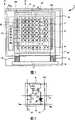
图1是表示本发明第一实施方式涉及的发光装置1的结构的一部分的概略平面图。FIG. 1 is a schematic plan view showing a part of the structure of a light emitting device 1 according to a first embodiment of the present invention.
图2是表示发光装置1的单位电路P的细节的电路图。FIG. 2 is a circuit diagram showing details of a unit circuit P of the light emitting device 1 .
图3是图1所示的发光装置1的A-A’线向视剖视图。Fig. 3 is a sectional view taken along line A-A' of the light emitting device 1 shown in Fig. 1 .
图4是表示本发明第二实施方式涉及的发光装置2的结构的一部分的概略平面图。4 is a schematic plan view showing a part of the structure of a
图5是表示图4所示的发光装置2的B-B’线向视剖视图。Fig. 5 is a sectional view taken along line B-B' of the
图6是本发明第三实施方式涉及的发光装置3的一部分的剖视图。Fig. 6 is a cross-sectional view of part of a
图7是本发明第四实施方式涉及的发光装置4的一部分的剖视图。7 is a cross-sectional view of a part of a
图8是表示把本发明实施方式涉及的各发光装置作为显示装置采用的便携式个人电脑的结构的图。FIG. 8 is a diagram showing the configuration of a portable personal computer employing each of the light emitting devices according to the embodiment of the present invention as a display device.
图9是表示把本发明实施方式涉及的各发光装置作为显示装置采用的移动电话的结构的图。9 is a diagram showing the configuration of a mobile phone employing each of the light-emitting devices according to the embodiment of the present invention as a display device.
图10是表示把本发明实施方式涉及的各发光装置作为显示装置采用的便携式信息终端的结构的图。10 is a diagram showing the configuration of a portable information terminal employing each of the light emitting devices according to the embodiment of the present invention as a display device.
图11是以往的发光装置(单层结构)的端部的剖视图。Fig. 11 is a cross-sectional view of an end portion of a conventional light-emitting device (single-layer structure).
图12是以往的发光装置(多层结构)的端部的剖视图。Fig. 12 is a cross-sectional view of an end portion of a conventional light-emitting device (multilayer structure).
图中:1~4-发光装置;10-基板;12-扫描线驱动电路;13-扫描线;14-数据线;15-电流供给线;16-阴极用电源布线(布线);17-布线层;18-绝缘膜;19-阴极层;20-周边壁(周边层);2000-个人电脑(电子设备);21-阴极保护膜;22-有机缓冲膜;23、24-气体阻挡膜;25-对置基板(其他基板);26、27-密封部;3000-移动电话(电子设备);4000-便携式信息终端(电子设备);G-发光区域;H-周边区域;P-单位电路。In the figure: 1-4-light-emitting device; 10-substrate; 12-scanning line driving circuit; 13-scanning line; 14-data line; 15-current supply line; 16-cathode power supply wiring (wiring); 17-wiring Layer; 18-insulating film; 19-cathode layer; 20-peripheral wall (peripheral layer); 2000-personal computer (electronic equipment); 21-cathode protection film; 22-organic buffer film; 23,24-gas barrier film; 25-opposed substrate (other substrate); 26, 27-sealing part; 3000-mobile phone (electronic device); 4000-portable information terminal (electronic device); G-light-emitting area; H-peripheral area; P-unit circuit .
具体实施方式Detailed ways
下面,参照附图,说明本发明的实施方式。须指出的是,在附图中,各部的尺寸的比例与实际的适宜不同。Hereinafter, embodiments of the present invention will be described with reference to the drawings. It should be noted that in the drawings, the ratio of the dimensions of each part is different from the actual ratio.
<第一实施方式><First Embodiment>
图1是表示本发明第一实施方式的发光装置1的结构的一部分的概略平面图。发光装置1具有基板10。在基板10的端部形成连接端子11。对连接端子11,从外部的电路供给各种信号或电源电压。此外,在基板10上设置矩形的像素区G、位于像素区G和基板10的外周之间的周边区域H。在周边区域H形成扫描线驱动电路12和数据线驱动电路(省略图示)。在像素区G形成多条扫描线13和多条数据线14,在这些交叉点的每一个附近设置多个单位电路(像素电路)P。FIG. 1 is a schematic plan view showing part of the structure of a light emitting device 1 according to a first embodiment of the present invention. The lighting device 1 has a
图2是表示发光装置1的单位电路P的细节的电路图。各单位电路P包含n沟道型晶体管T1、p沟道型晶体管T2、电容元件C和OLED50。p沟道型晶体管T2的源电极连接在电流供给线15上,其漏电极连接在OLED50的阳极81上。电流供给线15是用于供给驱动OLED50用的电流的布线。此外,在晶体管T2的源电极和栅电极之间设置电容元件C。n沟道型晶体管T1的栅电极连接在扫描线13上,其源电极连接在数据线14上,其漏电极与晶体管T2的栅极连接。FIG. 2 is a circuit diagram showing details of a unit circuit P of the light emitting device 1 . Each unit circuit P includes an n-channel transistor T1 , a p-channel transistor T2 , a capacitive element C, and an
单位电路P中,如果扫描线驱动电路12选择与该单位电路P对应的扫描线13,晶体管T1就导通,把从数据线驱动电路(省略图示)通过数据线14供给的数据信号在内部的电容元件C中保持。而且,晶体管T2对OLED50供给与数据信号的电平对应的电流。据此,OLED50以与数据信号的电平对应的亮度发光。In the unit circuit P, if the scanning
如图1所示,在基板10上的周边区域H,阴极用电源布线16形成为包围像素区G的コ字状。即,阴极用电源布线16沿着像素区G的周围直线状延伸,在2个地方弯曲为大致直角。阴极用电源布线16配置在扫描线驱动电路12和像素区G之间。阴极用电源布线16是用于流过驱动OLED50的电流的布线。OLED50具有阳极(2个电极中的一方)81、阴极(2个电极中的另一方)和夹在两个电极之间的发光功能层。As shown in FIG. 1 , in the peripheral region H on the
图3是图1所示的发光装置1的A-A’线向视剖视图。在基板10上形成以氧化硅为主体的底层保护层(省略图示),在其上形成包含金属布线层的布线层17。在布线层17中,在像素区G内,针对各单位电路P而设置有晶体管T1和晶体管T2。此外,在布线层17中,在周边区域H内设置扫描线驱动电路12或数据线驱动电路(省略图示)。这些电路具有晶体管、电容元件等电路元件。金属布线层由铝等具有导电性的材料形成,其一部分成为各晶体管的电极、扫描线13、数据线14、电流供给线15、阴极用电源布线16。Fig. 3 is a sectional view taken along line A-A' of the light emitting device 1 shown in Fig. 1 . An underlying protective layer (not shown) mainly composed of silicon oxide is formed on the
在布线层17上,在像素区G内,按各单位电路P设置有OLED50的阳极81。各阳极81通过对应的接触孔与包含自己的单位电路P内的晶体管T2的漏电极电连接。在布线层17和各阳极81上形成绝缘膜18。绝缘膜18是把OLED50的阳极81和阴极彼此绝缘的膜,由丙烯酸树脂或聚酰亚胺形成,在像素区G中,以只有各阳极81的上面的至少一部分露出的方式覆盖布线层17和阳极81。绝缘膜18的外端位于周边区域H。在由绝缘膜18包围的区域中,在阳极81上形成发光功能层82。发光功能层82的端面与绝缘膜18接触。发光功能层82具有由有机EL材料形成的发光层。有机EL材料可以是低分子材料,也可以是高分子材料。发光功能层82除了发光层,还可以具有空穴注入层、空穴输送层、电子输送层、空穴阻挡层和电子阻挡层的一部分或全部。On the
在绝缘膜18和发光功能层82上形成阴极层19。阴极层19由导电性材料形成,例如通过蒸镀来进行该形成。阴极层19可以由多层构成。此外,阴极层19在整个像素区G和周边区域H形成,在多个单位电路P中公共设置。阴极层19的一部分成为对应的单位电路P内的OLED50的阴极。在周边区域H中,阴极层19与阴极用电源布线16重叠,通过形成在布线层17上的接触孔CH而与阴极用电源布线16电连接。阴极层19的边缘位于布线层17上。The
如上所述,发光功能层82按照各单位电路P设置,绝缘膜18设置为划分形成发光功能层82的区域。这里,在俯视观察时,采取发光功能层82的一部分和绝缘膜18彼此重叠的结构,但是并不局限于此,也可以采取专用地设置发光功能层82和绝缘膜18的结构(发光功能层和绝缘膜18彼此不重叠的结构)。As described above, the light-emitting
此外,作为其他结构例,发光功能层和阴极层19至少在像素区中,对于多个单位电路P公共设置。这时,发光功能层发光的区域由绝缘膜18划分,按照各阳极81,设置发光的区域。该发光的区域也可以与绝缘膜18的边缘部等、绝缘膜18重叠。这里,发光功能层和阴极层19设置为覆盖绝缘膜18和阳极81之上。In addition, as another structural example, the light-emitting functional layer and the
在布线层17上,在周边区域H形成周边壁20。周边壁20由丙烯酸树脂或聚酰亚胺形成。这里,希望用与绝缘膜18相同的工艺统一形成。即本实施方式的绝缘膜18和周边壁20由同一绝缘层构成,该绝缘层被设置为:把OLED50的2个电极绝缘,并且覆盖扫描线驱动电路12或数据线驱动电路等驱动电路。周边壁20是用于保护扫描线驱动电路12或数据线驱动电路(省略图示)的结构物,设置为覆盖描线驱动电路12或数据线驱动电路(省略图示)。A
在布线层17、阴极层19和周边壁20上形成保护OLED50不受外部气体影响的密封层。层叠3层的薄膜而构成密封层。3层的薄膜是:在布线层17、阴极层19和周边壁20上形成的阴极保护膜21;形成在阴极保护膜21上的有机缓冲膜22;在布线层17、阴极保护膜21和有机缓冲膜22上形成的气体阻挡膜23。A sealing layer is formed on the
阴极保护膜21是为了保护阴极层19和容易形成有机缓冲膜22,至少覆盖阴极层19并延伸。须指出的是,在本实施方式中,阴极保护膜21的边缘位于周边壁20的外侧。此外,阴极保护膜21由无机材料形成。作为无机材料,能列举硅氧化物、硅氮氧化物等硅氧化物、氧化钛等金属氧化物等无机氧化物。The
有机缓冲膜22是用于填补由于绝缘膜18的形状的影响而在各像素中产生的阴极保护膜21的阶差,防止气体阻挡膜23中的应力集中,由有机材料形成。有机缓冲膜22例如由涂敷法(印刷法)形成,以使上表面变得平坦。有机缓冲膜22覆盖阴极层19并延伸,至少在像素区内,至少在绝缘膜18的上方形成。有机缓冲膜22的边缘221是包围像素区G的大致长方形,位于绝缘膜18和周边壁20之间。有机缓冲膜22的边缘221中的3个边位于阴极用电源布线16上。阴极用电源布线16上的边缘221与阴极用电源布线16大致平行。The
气体阻挡膜23是为了防止氧或水分等外部气体的侵入的膜,覆盖阴极保护膜21和有机缓冲膜22并延伸。此外,气体阻挡膜23在有机缓冲膜22的边缘221附近,跨越与有机缓冲膜22的厚度对应的长度,并沿相对于基板10倾斜的方向延伸。此外,气体阻挡膜23由硅化合物或硅氧化物等无机材料形成。在本实施方式中,气体阻挡膜23在设置了周边壁20的区域和设置了绝缘膜18的区域之间的区域中,与底层(在本实施方式中,阴极保护膜21)接触。底层也可以是布线层17中包含的绝缘膜。该底层希望是硅氧化物、硅氮氧化物、硅氮化物等硅化合物。The
有机缓冲膜22的边缘221的位置在发光装置1的每个个体中有可能在图3所示的L1的范围中偏移。可是,边缘221的位置即使在该范围中偏移,在基板10的边缘和覆盖OLED50以及绝缘膜18的有机缓冲膜22的边缘221之间也依旧存在周边壁20。因此,根据发光装置1,即使边缘221的位置精度低,如果周边壁20的边缘的位置精度高,就能使框的宽度变窄。The position of the
而且,在发光装置1中,能在形成OLED50之前形成周边壁20。即,在周边壁20的形成过程中能采用其边缘的位置精度提高的形成方法。Furthermore, in the light-emitting device 1, the
此外,能利用对OLED50不带来深刻的不良影响且位置精度高的形成方法形成构成密封层的3层薄膜中的有机缓冲膜22以外的膜(阴极保护膜21和气体阻挡膜23)。In addition, films other than the organic buffer film 22 (cathode
因此,根据发光装置1,即使用位置精度低的形成方法形成构成密封层的有机缓冲膜22,也能实现窄框化。Therefore, according to the light-emitting device 1 , even if the
此外,在发光装置1中,有机缓冲膜22的边缘221中的3个边与阴极用电源布线16大致平行,并位于阴极用电源布线16上。即,有机缓冲膜22的边缘221的很多区间位于平坦的面上。因此,密封性能提高。须指出的是,配置在有机缓冲膜22的边缘221之下的布线并不局限于阴极用电源布线16。例如,也可以是连接在电流供给线15上且用于对单位电路P供给电流的布线。须指出的是,上述的单位电路P的结构不过是一个例子。In addition, in the light-emitting device 1 , three of the
须指出的是,如果换言本实施方式的特征,就变为以下那样。本实施方式的绝缘膜18和周边壁20设置在相同的绝缘层中,该绝缘层设置为覆盖像素区上和驱动电路上双方,在设置了像素区的区域和设置了驱动电路的区域之间具有不设置绝缘层的区域。有机缓冲膜22的边缘221位于不设置该绝缘层的区域每,在该区域中,气体阻挡膜23与底层接触。希望在不设置该绝缘层的区域设置连接在阴极用电源布线16或电流供给线15上的布线。这里,驱动电路可以是扫描线驱动电路、数据线驱动电路、检查电路。It should be noted that, in other words, the features of the present embodiment are as follows. The insulating
<第二实施方式><Second Embodiment>
图4是表示本发明第二实施方式的发光装置2的结构的一部分的概略平面图,图5是表示图4所示的发光装置2的B-B’线向视剖视图。发光装置2与发光装置1的不同点在于,密封层由1层的薄膜形成。在发光装置2中,在布线层17和阴极层19上形成保护OLED50不受外部气体影响的密封层。该密封层由1层的薄膜形成。该薄膜是形成在布线层17和阴极层19上的气体阻挡膜24。Fig. 4 is a schematic plan view showing a part of the structure of a
气体阻挡膜24是用于防止氧或水分等外部气体的侵入的膜,覆盖阴极层19并延伸。此外,气体阻挡膜24在绝缘膜18的外端附近,跨越与绝缘膜18的厚度对应的长度,并沿相对于基板10倾斜的方向延伸。在本实施方式中,气体阻挡膜23在设置了周边壁20的区域和设置了绝缘膜18的区域之间的区域中,至少与底层(本实施方式中,布线层17中包含的绝缘膜或布线层)接触。底层希望是硅氧化物、硅氮氧化物、硅氮化物等硅化合物。气体阻挡膜24的边缘241是包围像素区G的大致长方形,位于绝缘膜18和周边壁20之间。气体阻挡膜24的边缘241中的3个边位于阴极用电源布线16上。阴极用电源布线16上的边缘241与阴极用电源布线16大致平行。此外,气体阻挡膜24由硅化合物或硅氧化物等无机材料形成。气体阻挡膜24的形成方法能列举例如蒸镀法。The
气体阻挡膜24的边缘241的位置在发光装置2的每个个体中有可能在图5所示的L2的范围中偏移。可是,边缘241的位置即使在该范围中偏移,在基板10的边缘和覆盖OLED50以及绝缘膜18的气体阻挡膜24的边缘241之间也依旧存在周边壁20。因此,根据发光装置1,即使边缘241的位置精度低,如果周边壁20的边缘的位置精度高,就能使框的宽度变窄。因此,根据发光装置2,即使用位置精度低的形成方法形成构成密封层的气体阻挡膜24,也能实现窄框化。The position of the
此外,在发光装置2中,气体阻挡膜24的边缘241中的3个边与阴极用电源布线16大致平行,并位于阴极用电源布线16上。因此,密封性能提高。与发光装置1同样,须指出的是:配置在气体阻挡膜24的边缘241之下的布线并不局限于阴极用电源布线16,图2所示的单位电路P的结构不过是一个例子。In addition, in the light-emitting
须指出的是,如果换言本实施方式的特征,就变为以下那样。本实施方式的绝缘膜18和周边壁20在相同的绝缘层中设置,该绝缘层设置为覆盖像素区上和驱动电路上双方,在设置了像素区的区域和设置了驱动电路的区域之间具有不设置绝缘层的区域。气体阻挡膜23不设置该绝缘层的区域中与底层接触。在不设置该绝缘层的区域中设置连接在阴极用电源布线16或电流供给线15上的布线。这里,驱动电路可以是扫描线驱动电路、数据线驱动电路、检察电路。It should be noted that, in other words, the features of the present embodiment are as follows. The insulating
<第三实施方式><Third Embodiment>
图6是本发明第三实施方式的发光装置3的一部分的剖视图。发光装置3与发光装置1的不同点在于,除了基板10以外,还具有基板。其他基板是隔着OLED50而与基板10相对的对置基板25。对置基板25例如是滤色器基板,由密封部26支撑。Fig. 6 is a cross-sectional view of part of a
在基板10的设置了OLED50的一侧和对置基板25之间填充由树脂构成的填充材料。A filling material made of resin is filled between the side of the
在第一和第二实施方式中,通过气体阻挡膜23,防止外部气体到达OLED50,但是在本实施方式中,通过填充材料、密封部26和对置基板25,进一步提高密封性能。In the first and second embodiments, the
密封部26例如由树脂形成,以包围绝缘膜18的方式设置在气体阻挡膜23上。密封部26的一端固定在气体阻挡膜23上,另一端固定在对置基板25上。气体阻挡膜23的与密封部26接触的部分是周边壁20上的部分。即,密封部26、和气体阻挡膜23的在相对于基板10倾斜的方向上延伸的部分231彼此隔开。The sealing
如果部分231与密封部26接触,则由于应力集中,气体阻挡膜23容易破损,但是如上所述,在发光装置3中,两者不接触。此外,周边壁20的上表面是大致平坦的。因此,根据发光装置3,除了在发光装置1中取得的效果以外,还能取得把气体阻挡膜23破损的可能性抑制得很低的效果。If the
与气体阻挡膜23和有机缓冲膜22覆盖周边壁20和像素区,并在其外侧的区域配置密封部26的结构相比,在本实施方式中,密封部26和周边壁20重叠,所以能使发光装置3窄框化。此外,能在为了使有机缓冲膜22的边缘221和密封部26不重叠而设置的边缘区域中配置阴极用电源布线16等布线,所以能进一步谋求发光装置3的窄框化。Compared with the structure in which the
<第四实施方式><Fourth Embodiment>
图7是本发明第四实施方式的发光装置4的一部分的剖视图。发光装置4与发光装置2的不同点在于,除了基板10以外,还具有对置基板25。对置基板25由密封部27支撑。密封部27例如由树脂形成,以包围绝缘膜18的方式设置在布线层17和周边壁20上。密封部27的一端固定在布线层17和周边壁20上,另一端固定在对置基板25上。密封部27、和气体阻挡膜24的在相对于基板10倾斜的方向上延伸的部分242彼此隔开。Fig. 7 is a cross-sectional view of a part of a
如果部分242与密封部27接触,则由于应力集中,气体阻挡膜24容易破损,但是如上所述,在发光装置4中两者不接触。密封部27和气体阻挡膜24彼此隔开。因此,根据发光装置4,除了在发光装置2中取得的效果以外,还能取得把气体阻挡膜24破损的可能性抑制得很低的效果。If the
此外,与第三实施方式同样,能使发光装置4为窄框。In addition, similarly to the third embodiment, the
<变形例><Modification>
在上述的各实施方式中,密封层由1层或3层的薄膜构成,但是也可以由2层的薄膜构成,也可以由4层以上的薄膜构成。无论是哪种情况,最大膜厚最厚的膜由形成的膜的边缘的位置精度低的方法形成。此外,由形成的膜的边缘的位置精度低的形成方法形成的膜可以是多层。此外,由周边壁保护的电路并不局限于扫描线驱动电路,也可以是数据线驱动电路或检查电路。再有,有周边壁保护的部件并不局限于电路。例如,也可以由周边壁保护布线。此外,发光元件并不局限于OLED。In each of the above-mentioned embodiments, the sealing layer is composed of one or three layers of films, but may also be composed of two layers of films, or may be composed of four or more layers of films. In either case, the film with the thickest maximum film thickness is formed by a method in which the edge position accuracy of the formed film is low. In addition, a film formed by a forming method in which the edge position accuracy of the formed film is low may be multilayered. In addition, the circuit protected by the peripheral wall is not limited to the scanning line driving circuit, and may be a data line driving circuit or an inspection circuit. Also, the components protected by the peripheral wall are not limited to electrical circuits. For example, the wiring may be protected by a peripheral wall. In addition, the light emitting element is not limited to OLED.
<应用例><Application example>
下面,说明应用上述的实施方式的各发光装置的电子设备。Next, an electronic device to which each light-emitting device of the above-mentioned embodiment is applied will be described.
图8是表示把上述的各发光装置作为显示装置采用的便携式个人电脑的结构的图。个人电脑2000具有显示装置2003和主体部2010。在主体部2010设置电源开关2001和键盘2002。Fig. 8 is a diagram showing the configuration of a portable personal computer employing each of the light-emitting devices described above as a display device. The
图9是表示把上述的各发光装置作为显示装置采用的移动电话的结构的图。移动电话3000具有多个操作按钮3001和滚动按钮3002、显示装置3003。通过操作滚动按钮3002,从而使显示装置3003上显示的画面滚动。Fig. 9 is a diagram showing the configuration of a mobile phone employing the above-mentioned light-emitting devices as a display device.
图10是表示把上述的各发光装置作为显示装置采用的便携式信息终端(PDA:Personal Digital Assistants)的结构的图。便携式信息终端4000具有多个操作按钮4001和电源开关4002、显示装置4003。如果操作电源开关4002,就在显示装置4003上显示地址本和日程表等各种信息。FIG. 10 is a diagram showing the configuration of a portable information terminal (PDA: Personal Digital Assistants) employing each of the light emitting devices described above as a display device. The
须指出的是,作为应用本发明的发光装置的电子设备,除了图8~图10所示的电子设备以外,还能列举电视或摄影机等能显示视频的设备、电子照相方式的图像形成装置。It should be noted that, as electronic equipment to which the light-emitting device of the present invention is applied, in addition to the electronic equipment shown in FIGS.
Claims (8)
Applications Claiming Priority (3)
| Application Number | Priority Date | Filing Date | Title |
|---|---|---|---|
| JP2006271575AJP4245032B2 (en) | 2006-10-03 | 2006-10-03 | LIGHT EMITTING DEVICE AND ELECTRONIC DEVICE |
| JP2006-271575 | 2006-10-03 | ||
| JP2006271575 | 2006-10-03 |
Publications (2)
| Publication Number | Publication Date |
|---|---|
| CN101160001Atrue CN101160001A (en) | 2008-04-09 |
| CN101160001B CN101160001B (en) | 2011-08-31 |
Family
ID=39260455
Family Applications (1)
| Application Number | Title | Priority Date | Filing Date |
|---|---|---|---|
| CN2007101622685AActiveCN101160001B (en) | 2006-10-03 | 2007-09-30 | Light-emitting device and electronic apparatus |
Country Status (5)
| Country | Link |
|---|---|
| US (1) | US7902755B2 (en) |
| JP (1) | JP4245032B2 (en) |
| KR (1) | KR101376130B1 (en) |
| CN (1) | CN101160001B (en) |
| TW (1) | TW200824489A (en) |
Cited By (17)
| Publication number | Priority date | Publication date | Assignee | Title |
|---|---|---|---|---|
| CN101866585A (en)* | 2010-04-13 | 2010-10-20 | 深圳市锐拓显示技术有限公司 | Pressure balancer for LED display screen |
| CN102256786A (en)* | 2008-12-30 | 2011-11-23 | 三星移动显示器株式会社 | Method for edge sealing a barrier film |
| WO2014056241A1 (en)* | 2012-10-12 | 2014-04-17 | 深圳市华星光电技术有限公司 | Organic light emitting diode and corresponding display device |
| CN103824871A (en)* | 2012-11-19 | 2014-05-28 | 三星显示有限公司 | Organic light-emitting display system and method of manufacturing the same |
| CN104067692A (en)* | 2012-01-23 | 2014-09-24 | 株式会社爱发科 | Element structure and manufacturing method of element structure |
| CN104464614A (en)* | 2013-09-18 | 2015-03-25 | 索尼公司 | Display device and electronic apparatus |
| CN104517999A (en)* | 2013-09-30 | 2015-04-15 | 三星显示有限公司 | Display device and method of manufacturing display device |
| CN105470406A (en)* | 2014-09-29 | 2016-04-06 | 乐金显示有限公司 | Organic light-emitting display device |
| CN105720079A (en)* | 2014-12-18 | 2016-06-29 | 株式会社日本显示器 | Organic electroluminescent display device |
| CN105954948A (en)* | 2016-02-04 | 2016-09-21 | 友达光电股份有限公司 | Display and method for manufacturing display |
| US9847505B2 (en) | 2014-10-17 | 2017-12-19 | Semiconductor Energy Laboratory Co., Ltd. | Light-emitting device, module, electronic device, and method for manufacturing light-emitting device |
| US9917282B2 (en) | 2015-07-30 | 2018-03-13 | Semiconductor Energy Laboratory Co., Ltd. | Manufacturing method of light-emitting device, light-emitting device, module, and electronic device |
| CN110085631A (en)* | 2014-12-11 | 2019-08-02 | 索尼公司 | Display device |
| CN111261096A (en)* | 2019-08-07 | 2020-06-09 | 友达光电股份有限公司 | Display device |
| CN112467055A (en)* | 2014-08-29 | 2021-03-09 | 三星显示有限公司 | Display device and method for manufacturing the same |
| CN112614960A (en)* | 2017-06-14 | 2021-04-06 | 乐金显示有限公司 | Display device and method for manufacturing the same |
| CN112928224A (en)* | 2019-12-05 | 2021-06-08 | 株式会社日本有机雷特显示器 | Self-luminous display panel and manufacturing method thereof |
Families Citing this family (31)
| Publication number | Priority date | Publication date | Assignee | Title |
|---|---|---|---|---|
| KR101886801B1 (en) | 2010-09-14 | 2018-08-10 | 삼성디스플레이 주식회사 | flat panel display integrated touch screen panel |
| JP2012248743A (en)* | 2011-05-30 | 2012-12-13 | Japan Display West Co Ltd | Semiconductor device, manufacturing method of the semiconductor device, display device, and electronic apparatus |
| JP2013016371A (en)* | 2011-07-05 | 2013-01-24 | Seiko Epson Corp | Electro-optical device and electronic apparatus |
| KR101980234B1 (en)* | 2012-10-30 | 2019-05-21 | 삼성디스플레이 주식회사 | Organic light emitting display device and the fabrication method thereof |
| KR102050434B1 (en)* | 2012-10-31 | 2019-11-29 | 엘지디스플레이 주식회사 | Flexible organic electroluminescent device and method for fabricating the same |
| JP6077279B2 (en)* | 2012-11-20 | 2017-02-08 | 株式会社ジャパンディスプレイ | Display device |
| KR101473309B1 (en)* | 2012-11-29 | 2014-12-16 | 삼성디스플레이 주식회사 | Display device and Organic luminescence display device |
| JP6267449B2 (en)* | 2013-03-15 | 2018-01-24 | 東京エレクトロン株式会社 | Organic device manufacturing method and organic device manufacturing apparatus |
| KR102034253B1 (en) | 2013-04-12 | 2019-10-21 | 삼성디스플레이 주식회사 | Organic light emitting display apparatus and the manufacturing method thereof |
| KR102117612B1 (en) | 2013-08-28 | 2020-06-02 | 삼성디스플레이 주식회사 | Organic light emitting display apparatus and the manufacturing method thereof |
| TW201513334A (en)* | 2013-09-30 | 2015-04-01 | Au Optronics Corp | Electroluminescent display panel |
| WO2015136670A1 (en)* | 2014-03-13 | 2015-09-17 | パイオニア株式会社 | Light emitting apparatus |
| JP6300231B2 (en) | 2014-06-25 | 2018-03-28 | パナソニック株式会社 | Organic EL device |
| JP6226312B2 (en)* | 2014-07-30 | 2017-11-08 | パナソニックIpマネジメント株式会社 | Organic EL device and manufacturing method thereof |
| KR102317715B1 (en)* | 2014-09-30 | 2021-10-25 | 엘지디스플레이 주식회사 | Organic light emitting display apparatus and manufacturing the same |
| CN105206620B (en)* | 2015-08-27 | 2017-02-15 | 京东方科技集团股份有限公司 | Thin-film packaging structure and preparation method thereof, and display apparatus |
| KR102427249B1 (en)* | 2015-10-16 | 2022-08-01 | 삼성디스플레이 주식회사 | display device |
| KR102407569B1 (en)* | 2015-10-31 | 2022-06-10 | 엘지디스플레이 주식회사 | Organic light emitting display device |
| KR102446425B1 (en) | 2015-11-17 | 2022-09-23 | 삼성디스플레이 주식회사 | Display device and method of manufacturing display device |
| KR102509079B1 (en)* | 2015-11-30 | 2023-03-09 | 엘지디스플레이 주식회사 | Organic light emitting display |
| KR102407869B1 (en) | 2016-02-16 | 2022-06-13 | 삼성디스플레이 주식회사 | Organic light emitting display device and the fabrication method thereof |
| KR102451726B1 (en) | 2016-03-28 | 2022-10-07 | 삼성디스플레이 주식회사 | Display device and the method of manufacturing thereof |
| JP2018036896A (en)* | 2016-08-31 | 2018-03-08 | 株式会社ジャパンディスプレイ | Touch sensor and display device |
| KR102799673B1 (en)* | 2016-11-29 | 2025-04-22 | 엘지디스플레이 주식회사 | Organic light emitting display device |
| KR102583813B1 (en)* | 2017-12-13 | 2023-09-26 | 엘지디스플레이 주식회사 | Display apparatus |
| CN108986667B (en)* | 2018-08-24 | 2020-12-04 | 武汉天马微电子有限公司 | Display panel, driving method thereof and display device |
| CN109243305B (en)* | 2018-09-17 | 2021-10-12 | 京东方科技集团股份有限公司 | Display panel, display device, and method for manufacturing display panel |
| CN110970462B (en)* | 2018-09-29 | 2022-10-14 | 京东方科技集团股份有限公司 | Display substrate, method for manufacturing the same, and display device |
| WO2020181467A1 (en)* | 2019-03-11 | 2020-09-17 | Boe Technology Group Co., Ltd. | Display substrate, display apparatus, method of fabricating display substrate |
| KR102096058B1 (en)* | 2019-05-13 | 2020-04-02 | 삼성디스플레이 주식회사 | Organic light emitting display device and the fabrication method thereof |
| KR102218650B1 (en)* | 2020-05-26 | 2021-02-23 | 삼성디스플레이 주식회사 | Organic light emitting display apparatus and the manufacturing method thereof |
Family Cites Families (12)
| Publication number | Priority date | Publication date | Assignee | Title |
|---|---|---|---|---|
| JP3830238B2 (en) | 1997-08-29 | 2006-10-04 | セイコーエプソン株式会社 | Active matrix type device |
| US7109653B2 (en)* | 2002-01-15 | 2006-09-19 | Seiko Epson Corporation | Sealing structure with barrier membrane for electronic element, display device, electronic apparatus, and fabrication method for electronic element |
| US7038377B2 (en)* | 2002-01-16 | 2006-05-02 | Seiko Epson Corporation | Display device with a narrow frame |
| SG143063A1 (en)* | 2002-01-24 | 2008-06-27 | Semiconductor Energy Lab | Light emitting device and method of manufacturing the same |
| JP4627966B2 (en)* | 2002-01-24 | 2011-02-09 | 株式会社半導体エネルギー研究所 | Light emitting device and manufacturing method thereof |
| JP3729262B2 (en) | 2002-08-29 | 2005-12-21 | セイコーエプソン株式会社 | ELECTROLUMINESCENT DEVICE AND ELECTRONIC DEVICE |
| JP4138672B2 (en)* | 2003-03-27 | 2008-08-27 | セイコーエプソン株式会社 | Manufacturing method of electro-optical device |
| US8350466B2 (en)* | 2004-09-17 | 2013-01-08 | Semiconductor Energy Laboratory Co., Ltd. | Display device and manufacturing method thereof |
| US8772783B2 (en)* | 2004-10-14 | 2014-07-08 | Semiconductor Energy Laboratory Co., Ltd. | Display device |
| ATE476757T1 (en)* | 2004-10-21 | 2010-08-15 | Lg Display Co Ltd | ORGANIC ELECTROLUMINESCENT DEVICE AND METHOD OF PRODUCTION |
| JP2006222071A (en)* | 2005-01-17 | 2006-08-24 | Seiko Epson Corp | LIGHT EMITTING DEVICE, LIGHT EMITTING DEVICE MANUFACTURING METHOD, AND ELECTRONIC DEVICE |
| JP4631683B2 (en)* | 2005-01-17 | 2011-02-16 | セイコーエプソン株式会社 | Light emitting device and electronic device |
- 2006
- 2006-10-03JPJP2006271575Apatent/JP4245032B2/enactiveActive
- 2007
- 2007-09-07USUS11/851,771patent/US7902755B2/enactiveActive
- 2007-09-28KRKR1020070097936Apatent/KR101376130B1/enactiveActive
- 2007-09-29TWTW096136639Apatent/TW200824489A/enunknown
- 2007-09-30CNCN2007101622685Apatent/CN101160001B/enactiveActive
Cited By (39)
| Publication number | Priority date | Publication date | Assignee | Title |
|---|---|---|---|---|
| CN102256786A (en)* | 2008-12-30 | 2011-11-23 | 三星移动显示器株式会社 | Method for edge sealing a barrier film |
| CN101866585A (en)* | 2010-04-13 | 2010-10-20 | 深圳市锐拓显示技术有限公司 | Pressure balancer for LED display screen |
| CN101866585B (en)* | 2010-04-13 | 2012-06-20 | 深圳市锐拓显示技术有限公司 | Pressure balancer for LED display screen |
| CN104067692A (en)* | 2012-01-23 | 2014-09-24 | 株式会社爱发科 | Element structure and manufacturing method of element structure |
| WO2014056241A1 (en)* | 2012-10-12 | 2014-04-17 | 深圳市华星光电技术有限公司 | Organic light emitting diode and corresponding display device |
| CN103824871A (en)* | 2012-11-19 | 2014-05-28 | 三星显示有限公司 | Organic light-emitting display system and method of manufacturing the same |
| CN103824871B (en)* | 2012-11-19 | 2019-05-07 | 三星显示有限公司 | Organic light-emitting display system and manufacturing method thereof |
| CN104464614B (en)* | 2013-09-18 | 2017-10-24 | 株式会社日本有机雷特显示器 | Display device and electronic equipment |
| CN104464614A (en)* | 2013-09-18 | 2015-03-25 | 索尼公司 | Display device and electronic apparatus |
| US9830862B2 (en) | 2013-09-18 | 2017-11-28 | Joled Inc. | Display device and electronic apparatus |
| CN104517999A (en)* | 2013-09-30 | 2015-04-15 | 三星显示有限公司 | Display device and method of manufacturing display device |
| US12156435B2 (en) | 2013-09-30 | 2024-11-26 | Samsung Display Co., Ltd. | Display devices and methods of manufacturing display devices |
| CN104517999B (en)* | 2013-09-30 | 2019-08-16 | 三星显示有限公司 | Display device and method of manufacturing display device |
| US11289553B2 (en) | 2013-09-30 | 2022-03-29 | Samsung Display Co., Ltd. | Display devices and methods of manufacturing display devices |
| CN112467055A (en)* | 2014-08-29 | 2021-03-09 | 三星显示有限公司 | Display device and method for manufacturing the same |
| US11930661B2 (en) | 2014-08-29 | 2024-03-12 | Samsung Display Co., Ltd. | Display apparatus having encapsulating layers terminating at a peripheral area of a substrate and method of manufacturing the same |
| US9911943B2 (en) | 2014-09-29 | 2018-03-06 | Lg Display Co., Ltd. | Organic light-emitting display device including buffer layers |
| CN105470406A (en)* | 2014-09-29 | 2016-04-06 | 乐金显示有限公司 | Organic light-emitting display device |
| CN105470406B (en)* | 2014-09-29 | 2017-08-08 | 乐金显示有限公司 | Organic light-emitting display device |
| US11778850B2 (en) | 2014-10-17 | 2023-10-03 | Semiconductor Energy Laboratory Co., Ltd. | Light-emitting device, module, electronic device, and method for manufacturing light-emitting device |
| US10270057B2 (en) | 2014-10-17 | 2019-04-23 | Semiconductor Energy Laboratory Co., Ltd. | Light-emitting device, module, electronic device, and method for manufacturing light-emitting device |
| US9847505B2 (en) | 2014-10-17 | 2017-12-19 | Semiconductor Energy Laboratory Co., Ltd. | Light-emitting device, module, electronic device, and method for manufacturing light-emitting device |
| US10629843B2 (en) | 2014-10-17 | 2020-04-21 | Semiconductor Energy Laboratory Co., Ltd. | Light-emitting device, module, electronic device, and method for manufacturing light-emitting device |
| US11189817B2 (en) | 2014-10-17 | 2021-11-30 | Semiconductor Energy Laboratory Co., Ltd. | Light-emitting device, module, electronic device, and method for manufacturing light-emitting device |
| CN110085631B (en)* | 2014-12-11 | 2023-05-12 | 索尼公司 | display device |
| CN110085631A (en)* | 2014-12-11 | 2019-08-02 | 索尼公司 | Display device |
| CN105720079A (en)* | 2014-12-18 | 2016-06-29 | 株式会社日本显示器 | Organic electroluminescent display device |
| US10020353B2 (en) | 2014-12-18 | 2018-07-10 | Japan Display Inc. | Organic electroluminescent display device |
| US10804503B2 (en) | 2015-07-30 | 2020-10-13 | Semiconductor Energy Laboratory Co., Ltd. | Manufacturing method of light-emitting device, light-emitting device, module, and electronic device |
| US11411208B2 (en) | 2015-07-30 | 2022-08-09 | Semiconductor Energy Laboratory Co., Ltd. | Manufacturing method of light-emitting device, light-emitting device, module, and electronic device |
| US10135037B2 (en) | 2015-07-30 | 2018-11-20 | Semiconductor Energy Laboratory Co., Ltd. | Manufacturing method of light-emitting device, light-emitting device, module, and electronic device |
| US9917282B2 (en) | 2015-07-30 | 2018-03-13 | Semiconductor Energy Laboratory Co., Ltd. | Manufacturing method of light-emitting device, light-emitting device, module, and electronic device |
| CN105954948B (en)* | 2016-02-04 | 2019-05-31 | 友达光电股份有限公司 | Display and method for manufacturing display |
| CN105954948A (en)* | 2016-02-04 | 2016-09-21 | 友达光电股份有限公司 | Display and method for manufacturing display |
| CN112614960A (en)* | 2017-06-14 | 2021-04-06 | 乐金显示有限公司 | Display device and method for manufacturing the same |
| CN112614960B (en)* | 2017-06-14 | 2024-04-05 | 乐金显示有限公司 | Display device and method for manufacturing the same |
| CN111261096B (en)* | 2019-08-07 | 2021-03-19 | 友达光电股份有限公司 | display device |
| CN111261096A (en)* | 2019-08-07 | 2020-06-09 | 友达光电股份有限公司 | Display device |
| CN112928224A (en)* | 2019-12-05 | 2021-06-08 | 株式会社日本有机雷特显示器 | Self-luminous display panel and manufacturing method thereof |
Also Published As
| Publication number | Publication date |
|---|---|
| KR20080031115A (en) | 2008-04-08 |
| JP2008091237A (en) | 2008-04-17 |
| US20080079360A1 (en) | 2008-04-03 |
| US7902755B2 (en) | 2011-03-08 |
| CN101160001B (en) | 2011-08-31 |
| KR101376130B1 (en) | 2014-03-19 |
| TW200824489A (en) | 2008-06-01 |
| JP4245032B2 (en) | 2009-03-25 |
Similar Documents
| Publication | Publication Date | Title |
|---|---|---|
| CN101160001A (en) | Light emitting devices and electronic equipment | |
| US10644257B2 (en) | Display device | |
| US20200235194A1 (en) | Display device | |
| US11782542B2 (en) | Display device | |
| US9716248B2 (en) | Organic light-emitting diode displays with reduced border area | |
| KR101492488B1 (en) | Light emitting device and electronic device | |
| JP5017851B2 (en) | LIGHT EMITTING DEVICE AND ELECTRONIC DEVICE | |
| JP4736757B2 (en) | LIGHT EMITTING DEVICE AND ELECTRONIC DEVICE | |
| TWI455643B (en) | Light-emitting device and electronic machine | |
| US8598782B2 (en) | Organic electroluminescent device and electronic apparatus | |
| JP4742835B2 (en) | LIGHT EMITTING DEVICE AND ELECTRONIC DEVICE | |
| US9704933B2 (en) | Organic electroluminescent device | |
| JP5447457B2 (en) | LIGHT EMITTING DEVICE AND ELECTRONIC DEVICE | |
| JP5062105B2 (en) | LIGHT EMITTING DEVICE AND ELECTRONIC DEVICE | |
| US10854688B2 (en) | Display panel and electronic apparatus | |
| KR20190026351A (en) | Eletroluminescence display device | |
| CN120112091B (en) | Display panel and display device | |
| JP2009059531A (en) | Organic el display device | |
| KR20060116516A (en) | Wiring structure of organic electroluminescent panel and organic electroluminescent panel | |
| KR20090111773A (en) | Organic EL Devices and Electronic Devices |
Legal Events
| Date | Code | Title | Description |
|---|---|---|---|
| C06 | Publication | ||
| PB01 | Publication | ||
| C10 | Entry into substantive examination | ||
| SE01 | Entry into force of request for substantive examination | ||
| C14 | Grant of patent or utility model | ||
| GR01 | Patent grant |