CN101159238A - Electronic device and manufacturing method thereof - Google Patents
Electronic device and manufacturing method thereofDownload PDFInfo
- Publication number
- CN101159238A CN101159238ACNA2007101499708ACN200710149970ACN101159238ACN 101159238 ACN101159238 ACN 101159238ACN A2007101499708 ACNA2007101499708 ACN A2007101499708ACN 200710149970 ACN200710149970 ACN 200710149970ACN 101159238 ACN101159238 ACN 101159238A
- Authority
- CN
- China
- Prior art keywords
- interconnection layer
- layer
- electronic device
- interconnection
- resin
- Prior art date
- Legal status (The legal status is an assumption and is not a legal conclusion. Google has not performed a legal analysis and makes no representation as to the accuracy of the status listed.)
- Granted
Links
Images


Classifications
- H—ELECTRICITY
- H01—ELECTRIC ELEMENTS
- H01L—SEMICONDUCTOR DEVICES NOT COVERED BY CLASS H10
- H01L23/00—Details of semiconductor or other solid state devices
- H01L23/28—Encapsulations, e.g. encapsulating layers, coatings, e.g. for protection
- H01L23/31—Encapsulations, e.g. encapsulating layers, coatings, e.g. for protection characterised by the arrangement or shape
- H01L23/3107—Encapsulations, e.g. encapsulating layers, coatings, e.g. for protection characterised by the arrangement or shape the device being completely enclosed
- H01L23/3121—Encapsulations, e.g. encapsulating layers, coatings, e.g. for protection characterised by the arrangement or shape the device being completely enclosed a substrate forming part of the encapsulation
- H01L23/3128—Encapsulations, e.g. encapsulating layers, coatings, e.g. for protection characterised by the arrangement or shape the device being completely enclosed a substrate forming part of the encapsulation the substrate having spherical bumps for external connection
- H—ELECTRICITY
- H01—ELECTRIC ELEMENTS
- H01L—SEMICONDUCTOR DEVICES NOT COVERED BY CLASS H10
- H01L21/00—Processes or apparatus adapted for the manufacture or treatment of semiconductor or solid state devices or of parts thereof
- H01L21/02—Manufacture or treatment of semiconductor devices or of parts thereof
- H01L21/04—Manufacture or treatment of semiconductor devices or of parts thereof the devices having potential barriers, e.g. a PN junction, depletion layer or carrier concentration layer
- H01L21/48—Manufacture or treatment of parts, e.g. containers, prior to assembly of the devices, using processes not provided for in a single one of the groups H01L21/18 - H01L21/326 or H10D48/04 - H10D48/07
- H01L21/4814—Conductive parts
- H01L21/4846—Leads on or in insulating or insulated substrates, e.g. metallisation
- H01L21/4857—Multilayer substrates
- H—ELECTRICITY
- H01—ELECTRIC ELEMENTS
- H01L—SEMICONDUCTOR DEVICES NOT COVERED BY CLASS H10
- H01L21/00—Processes or apparatus adapted for the manufacture or treatment of semiconductor or solid state devices or of parts thereof
- H01L21/67—Apparatus specially adapted for handling semiconductor or electric solid state devices during manufacture or treatment thereof; Apparatus specially adapted for handling wafers during manufacture or treatment of semiconductor or electric solid state devices or components ; Apparatus not specifically provided for elsewhere
- H01L21/683—Apparatus specially adapted for handling semiconductor or electric solid state devices during manufacture or treatment thereof; Apparatus specially adapted for handling wafers during manufacture or treatment of semiconductor or electric solid state devices or components ; Apparatus not specifically provided for elsewhere for supporting or gripping
- H01L21/6835—Apparatus specially adapted for handling semiconductor or electric solid state devices during manufacture or treatment thereof; Apparatus specially adapted for handling wafers during manufacture or treatment of semiconductor or electric solid state devices or components ; Apparatus not specifically provided for elsewhere for supporting or gripping using temporarily an auxiliary support
- H—ELECTRICITY
- H01—ELECTRIC ELEMENTS
- H01L—SEMICONDUCTOR DEVICES NOT COVERED BY CLASS H10
- H01L23/00—Details of semiconductor or other solid state devices
- H01L23/28—Encapsulations, e.g. encapsulating layers, coatings, e.g. for protection
- H01L23/31—Encapsulations, e.g. encapsulating layers, coatings, e.g. for protection characterised by the arrangement or shape
- H01L23/3107—Encapsulations, e.g. encapsulating layers, coatings, e.g. for protection characterised by the arrangement or shape the device being completely enclosed
- H01L23/3135—Double encapsulation or coating and encapsulation
- H—ELECTRICITY
- H01—ELECTRIC ELEMENTS
- H01L—SEMICONDUCTOR DEVICES NOT COVERED BY CLASS H10
- H01L23/00—Details of semiconductor or other solid state devices
- H01L23/52—Arrangements for conducting electric current within the device in operation from one component to another, i.e. interconnections, e.g. wires, lead frames
- H01L23/538—Arrangements for conducting electric current within the device in operation from one component to another, i.e. interconnections, e.g. wires, lead frames the interconnection structure between a plurality of semiconductor chips being formed on, or in, insulating substrates
- H01L23/5389—Arrangements for conducting electric current within the device in operation from one component to another, i.e. interconnections, e.g. wires, lead frames the interconnection structure between a plurality of semiconductor chips being formed on, or in, insulating substrates the chips being integrally enclosed by the interconnect and support structures
- H—ELECTRICITY
- H01—ELECTRIC ELEMENTS
- H01L—SEMICONDUCTOR DEVICES NOT COVERED BY CLASS H10
- H01L25/00—Assemblies consisting of a plurality of semiconductor or other solid state devices
- H01L25/18—Assemblies consisting of a plurality of semiconductor or other solid state devices the devices being of the types provided for in two or more different main groups of the same subclass of H10B, H10D, H10F, H10H, H10K or H10N
- H—ELECTRICITY
- H05—ELECTRIC TECHNIQUES NOT OTHERWISE PROVIDED FOR
- H05K—PRINTED CIRCUITS; CASINGS OR CONSTRUCTIONAL DETAILS OF ELECTRIC APPARATUS; MANUFACTURE OF ASSEMBLAGES OF ELECTRICAL COMPONENTS
- H05K3/00—Apparatus or processes for manufacturing printed circuits
- H05K3/0058—Laminating printed circuit boards onto other substrates, e.g. metallic substrates
- H—ELECTRICITY
- H05—ELECTRIC TECHNIQUES NOT OTHERWISE PROVIDED FOR
- H05K—PRINTED CIRCUITS; CASINGS OR CONSTRUCTIONAL DETAILS OF ELECTRIC APPARATUS; MANUFACTURE OF ASSEMBLAGES OF ELECTRICAL COMPONENTS
- H05K3/00—Apparatus or processes for manufacturing printed circuits
- H05K3/46—Manufacturing multilayer circuits
- H05K3/4644—Manufacturing multilayer circuits by building the multilayer layer by layer, i.e. build-up multilayer circuits
- H05K3/4682—Manufacture of core-less build-up multilayer circuits on a temporary carrier or on a metal foil
- H—ELECTRICITY
- H01—ELECTRIC ELEMENTS
- H01L—SEMICONDUCTOR DEVICES NOT COVERED BY CLASS H10
- H01L2221/00—Processes or apparatus adapted for the manufacture or treatment of semiconductor or solid state devices or of parts thereof covered by H01L21/00
- H01L2221/67—Apparatus for handling semiconductor or electric solid state devices during manufacture or treatment thereof; Apparatus for handling wafers during manufacture or treatment of semiconductor or electric solid state devices or components; Apparatus not specifically provided for elsewhere
- H01L2221/683—Apparatus for handling semiconductor or electric solid state devices during manufacture or treatment thereof; Apparatus for handling wafers during manufacture or treatment of semiconductor or electric solid state devices or components; Apparatus not specifically provided for elsewhere for supporting or gripping
- H01L2221/68304—Apparatus for handling semiconductor or electric solid state devices during manufacture or treatment thereof; Apparatus for handling wafers during manufacture or treatment of semiconductor or electric solid state devices or components; Apparatus not specifically provided for elsewhere for supporting or gripping using temporarily an auxiliary support
- H01L2221/68345—Apparatus for handling semiconductor or electric solid state devices during manufacture or treatment thereof; Apparatus for handling wafers during manufacture or treatment of semiconductor or electric solid state devices or components; Apparatus not specifically provided for elsewhere for supporting or gripping using temporarily an auxiliary support used as a support during the manufacture of self supporting substrates
- H—ELECTRICITY
- H01—ELECTRIC ELEMENTS
- H01L—SEMICONDUCTOR DEVICES NOT COVERED BY CLASS H10
- H01L2224/00—Indexing scheme for arrangements for connecting or disconnecting semiconductor or solid-state bodies and methods related thereto as covered by H01L24/00
- H01L2224/01—Means for bonding being attached to, or being formed on, the surface to be connected, e.g. chip-to-package, die-attach, "first-level" interconnects; Manufacturing methods related thereto
- H01L2224/02—Bonding areas; Manufacturing methods related thereto
- H01L2224/04—Structure, shape, material or disposition of the bonding areas prior to the connecting process
- H01L2224/05—Structure, shape, material or disposition of the bonding areas prior to the connecting process of an individual bonding area
- H01L2224/0554—External layer
- H01L2224/05573—Single external layer
- H—ELECTRICITY
- H01—ELECTRIC ELEMENTS
- H01L—SEMICONDUCTOR DEVICES NOT COVERED BY CLASS H10
- H01L2224/00—Indexing scheme for arrangements for connecting or disconnecting semiconductor or solid-state bodies and methods related thereto as covered by H01L24/00
- H01L2224/01—Means for bonding being attached to, or being formed on, the surface to be connected, e.g. chip-to-package, die-attach, "first-level" interconnects; Manufacturing methods related thereto
- H01L2224/10—Bump connectors; Manufacturing methods related thereto
- H01L2224/12—Structure, shape, material or disposition of the bump connectors prior to the connecting process
- H01L2224/13—Structure, shape, material or disposition of the bump connectors prior to the connecting process of an individual bump connector
- H01L2224/13001—Core members of the bump connector
- H01L2224/1302—Disposition
- H01L2224/13025—Disposition the bump connector being disposed on a via connection of the semiconductor or solid-state body
- H—ELECTRICITY
- H01—ELECTRIC ELEMENTS
- H01L—SEMICONDUCTOR DEVICES NOT COVERED BY CLASS H10
- H01L2224/00—Indexing scheme for arrangements for connecting or disconnecting semiconductor or solid-state bodies and methods related thereto as covered by H01L24/00
- H01L2224/01—Means for bonding being attached to, or being formed on, the surface to be connected, e.g. chip-to-package, die-attach, "first-level" interconnects; Manufacturing methods related thereto
- H01L2224/10—Bump connectors; Manufacturing methods related thereto
- H01L2224/15—Structure, shape, material or disposition of the bump connectors after the connecting process
- H01L2224/16—Structure, shape, material or disposition of the bump connectors after the connecting process of an individual bump connector
- H01L2224/161—Disposition
- H01L2224/16135—Disposition the bump connector connecting between different semiconductor or solid-state bodies, i.e. chip-to-chip
- H01L2224/16145—Disposition the bump connector connecting between different semiconductor or solid-state bodies, i.e. chip-to-chip the bodies being stacked
- H01L2224/16146—Disposition the bump connector connecting between different semiconductor or solid-state bodies, i.e. chip-to-chip the bodies being stacked the bump connector connecting to a via connection in the semiconductor or solid-state body
- H—ELECTRICITY
- H01—ELECTRIC ELEMENTS
- H01L—SEMICONDUCTOR DEVICES NOT COVERED BY CLASS H10
- H01L2224/00—Indexing scheme for arrangements for connecting or disconnecting semiconductor or solid-state bodies and methods related thereto as covered by H01L24/00
- H01L2224/01—Means for bonding being attached to, or being formed on, the surface to be connected, e.g. chip-to-package, die-attach, "first-level" interconnects; Manufacturing methods related thereto
- H01L2224/10—Bump connectors; Manufacturing methods related thereto
- H01L2224/15—Structure, shape, material or disposition of the bump connectors after the connecting process
- H01L2224/16—Structure, shape, material or disposition of the bump connectors after the connecting process of an individual bump connector
- H01L2224/161—Disposition
- H01L2224/16151—Disposition the bump connector connecting between a semiconductor or solid-state body and an item not being a semiconductor or solid-state body, e.g. chip-to-substrate, chip-to-passive
- H01L2224/16221—Disposition the bump connector connecting between a semiconductor or solid-state body and an item not being a semiconductor or solid-state body, e.g. chip-to-substrate, chip-to-passive the body and the item being stacked
- H01L2224/16225—Disposition the bump connector connecting between a semiconductor or solid-state body and an item not being a semiconductor or solid-state body, e.g. chip-to-substrate, chip-to-passive the body and the item being stacked the item being non-metallic, e.g. insulating substrate with or without metallisation
- H—ELECTRICITY
- H01—ELECTRIC ELEMENTS
- H01L—SEMICONDUCTOR DEVICES NOT COVERED BY CLASS H10
- H01L2224/00—Indexing scheme for arrangements for connecting or disconnecting semiconductor or solid-state bodies and methods related thereto as covered by H01L24/00
- H01L2224/01—Means for bonding being attached to, or being formed on, the surface to be connected, e.g. chip-to-package, die-attach, "first-level" interconnects; Manufacturing methods related thereto
- H01L2224/10—Bump connectors; Manufacturing methods related thereto
- H01L2224/15—Structure, shape, material or disposition of the bump connectors after the connecting process
- H01L2224/17—Structure, shape, material or disposition of the bump connectors after the connecting process of a plurality of bump connectors
- H01L2224/171—Disposition
- H01L2224/1718—Disposition being disposed on at least two different sides of the body, e.g. dual array
- H01L2224/17181—On opposite sides of the body
- H—ELECTRICITY
- H01—ELECTRIC ELEMENTS
- H01L—SEMICONDUCTOR DEVICES NOT COVERED BY CLASS H10
- H01L2224/00—Indexing scheme for arrangements for connecting or disconnecting semiconductor or solid-state bodies and methods related thereto as covered by H01L24/00
- H01L2224/01—Means for bonding being attached to, or being formed on, the surface to be connected, e.g. chip-to-package, die-attach, "first-level" interconnects; Manufacturing methods related thereto
- H01L2224/26—Layer connectors, e.g. plate connectors, solder or adhesive layers; Manufacturing methods related thereto
- H01L2224/31—Structure, shape, material or disposition of the layer connectors after the connecting process
- H01L2224/32—Structure, shape, material or disposition of the layer connectors after the connecting process of an individual layer connector
- H01L2224/321—Disposition
- H01L2224/32135—Disposition the layer connector connecting between different semiconductor or solid-state bodies, i.e. chip-to-chip
- H01L2224/32145—Disposition the layer connector connecting between different semiconductor or solid-state bodies, i.e. chip-to-chip the bodies being stacked
- H—ELECTRICITY
- H01—ELECTRIC ELEMENTS
- H01L—SEMICONDUCTOR DEVICES NOT COVERED BY CLASS H10
- H01L2224/00—Indexing scheme for arrangements for connecting or disconnecting semiconductor or solid-state bodies and methods related thereto as covered by H01L24/00
- H01L2224/01—Means for bonding being attached to, or being formed on, the surface to be connected, e.g. chip-to-package, die-attach, "first-level" interconnects; Manufacturing methods related thereto
- H01L2224/26—Layer connectors, e.g. plate connectors, solder or adhesive layers; Manufacturing methods related thereto
- H01L2224/31—Structure, shape, material or disposition of the layer connectors after the connecting process
- H01L2224/32—Structure, shape, material or disposition of the layer connectors after the connecting process of an individual layer connector
- H01L2224/321—Disposition
- H01L2224/32151—Disposition the layer connector connecting between a semiconductor or solid-state body and an item not being a semiconductor or solid-state body, e.g. chip-to-substrate, chip-to-passive
- H01L2224/32221—Disposition the layer connector connecting between a semiconductor or solid-state body and an item not being a semiconductor or solid-state body, e.g. chip-to-substrate, chip-to-passive the body and the item being stacked
- H01L2224/32225—Disposition the layer connector connecting between a semiconductor or solid-state body and an item not being a semiconductor or solid-state body, e.g. chip-to-substrate, chip-to-passive the body and the item being stacked the item being non-metallic, e.g. insulating substrate with or without metallisation
- H—ELECTRICITY
- H01—ELECTRIC ELEMENTS
- H01L—SEMICONDUCTOR DEVICES NOT COVERED BY CLASS H10
- H01L2224/00—Indexing scheme for arrangements for connecting or disconnecting semiconductor or solid-state bodies and methods related thereto as covered by H01L24/00
- H01L2224/73—Means for bonding being of different types provided for in two or more of groups H01L2224/10, H01L2224/18, H01L2224/26, H01L2224/34, H01L2224/42, H01L2224/50, H01L2224/63, H01L2224/71
- H01L2224/732—Location after the connecting process
- H01L2224/73201—Location after the connecting process on the same surface
- H01L2224/73203—Bump and layer connectors
- H01L2224/73204—Bump and layer connectors the bump connector being embedded into the layer connector
- H—ELECTRICITY
- H01—ELECTRIC ELEMENTS
- H01L—SEMICONDUCTOR DEVICES NOT COVERED BY CLASS H10
- H01L2224/00—Indexing scheme for arrangements for connecting or disconnecting semiconductor or solid-state bodies and methods related thereto as covered by H01L24/00
- H01L2224/73—Means for bonding being of different types provided for in two or more of groups H01L2224/10, H01L2224/18, H01L2224/26, H01L2224/34, H01L2224/42, H01L2224/50, H01L2224/63, H01L2224/71
- H01L2224/732—Location after the connecting process
- H01L2224/73251—Location after the connecting process on different surfaces
- H01L2224/73253—Bump and layer connectors
- H—ELECTRICITY
- H01—ELECTRIC ELEMENTS
- H01L—SEMICONDUCTOR DEVICES NOT COVERED BY CLASS H10
- H01L2224/00—Indexing scheme for arrangements for connecting or disconnecting semiconductor or solid-state bodies and methods related thereto as covered by H01L24/00
- H01L2224/80—Methods for connecting semiconductor or other solid state bodies using means for bonding being attached to, or being formed on, the surface to be connected
- H01L2224/81—Methods for connecting semiconductor or other solid state bodies using means for bonding being attached to, or being formed on, the surface to be connected using a bump connector
- H01L2224/81001—Methods for connecting semiconductor or other solid state bodies using means for bonding being attached to, or being formed on, the surface to be connected using a bump connector involving a temporary auxiliary member not forming part of the bonding apparatus
- H01L2224/81005—Methods for connecting semiconductor or other solid state bodies using means for bonding being attached to, or being formed on, the surface to be connected using a bump connector involving a temporary auxiliary member not forming part of the bonding apparatus being a temporary or sacrificial substrate
- H—ELECTRICITY
- H01—ELECTRIC ELEMENTS
- H01L—SEMICONDUCTOR DEVICES NOT COVERED BY CLASS H10
- H01L2224/00—Indexing scheme for arrangements for connecting or disconnecting semiconductor or solid-state bodies and methods related thereto as covered by H01L24/00
- H01L2224/80—Methods for connecting semiconductor or other solid state bodies using means for bonding being attached to, or being formed on, the surface to be connected
- H01L2224/83—Methods for connecting semiconductor or other solid state bodies using means for bonding being attached to, or being formed on, the surface to be connected using a layer connector
- H01L2224/83001—Methods for connecting semiconductor or other solid state bodies using means for bonding being attached to, or being formed on, the surface to be connected using a layer connector involving a temporary auxiliary member not forming part of the bonding apparatus
- H01L2224/83005—Methods for connecting semiconductor or other solid state bodies using means for bonding being attached to, or being formed on, the surface to be connected using a layer connector involving a temporary auxiliary member not forming part of the bonding apparatus being a temporary or sacrificial substrate
- H—ELECTRICITY
- H01—ELECTRIC ELEMENTS
- H01L—SEMICONDUCTOR DEVICES NOT COVERED BY CLASS H10
- H01L2225/00—Details relating to assemblies covered by the group H01L25/00 but not provided for in its subgroups
- H01L2225/03—All the devices being of a type provided for in the same main group of the same subclass of class H10, e.g. assemblies of rectifier diodes
- H01L2225/04—All the devices being of a type provided for in the same main group of the same subclass of class H10, e.g. assemblies of rectifier diodes the devices not having separate containers
- H01L2225/065—All the devices being of a type provided for in the same main group of the same subclass of class H10
- H01L2225/06503—Stacked arrangements of devices
- H01L2225/06555—Geometry of the stack, e.g. form of the devices, geometry to facilitate stacking
- H01L2225/06565—Geometry of the stack, e.g. form of the devices, geometry to facilitate stacking the devices having the same size and there being no auxiliary carrier between the devices
- H—ELECTRICITY
- H01—ELECTRIC ELEMENTS
- H01L—SEMICONDUCTOR DEVICES NOT COVERED BY CLASS H10
- H01L25/00—Assemblies consisting of a plurality of semiconductor or other solid state devices
- H01L25/03—Assemblies consisting of a plurality of semiconductor or other solid state devices all the devices being of a type provided for in a single subclass of subclasses H10B, H10D, H10F, H10H, H10K or H10N, e.g. assemblies of rectifier diodes
- H01L25/04—Assemblies consisting of a plurality of semiconductor or other solid state devices all the devices being of a type provided for in a single subclass of subclasses H10B, H10D, H10F, H10H, H10K or H10N, e.g. assemblies of rectifier diodes the devices not having separate containers
- H01L25/065—Assemblies consisting of a plurality of semiconductor or other solid state devices all the devices being of a type provided for in a single subclass of subclasses H10B, H10D, H10F, H10H, H10K or H10N, e.g. assemblies of rectifier diodes the devices not having separate containers the devices being of a type provided for in group H10D89/00
- H01L25/0652—Assemblies consisting of a plurality of semiconductor or other solid state devices all the devices being of a type provided for in a single subclass of subclasses H10B, H10D, H10F, H10H, H10K or H10N, e.g. assemblies of rectifier diodes the devices not having separate containers the devices being of a type provided for in group H10D89/00 the devices being arranged next and on each other, i.e. mixed assemblies
- H—ELECTRICITY
- H01—ELECTRIC ELEMENTS
- H01L—SEMICONDUCTOR DEVICES NOT COVERED BY CLASS H10
- H01L2924/00—Indexing scheme for arrangements or methods for connecting or disconnecting semiconductor or solid-state bodies as covered by H01L24/00
- H01L2924/0001—Technical content checked by a classifier
- H01L2924/00014—Technical content checked by a classifier the subject-matter covered by the group, the symbol of which is combined with the symbol of this group, being disclosed without further technical details
- H—ELECTRICITY
- H01—ELECTRIC ELEMENTS
- H01L—SEMICONDUCTOR DEVICES NOT COVERED BY CLASS H10
- H01L2924/00—Indexing scheme for arrangements or methods for connecting or disconnecting semiconductor or solid-state bodies as covered by H01L24/00
- H01L2924/01—Chemical elements
- H01L2924/01079—Gold [Au]
- H—ELECTRICITY
- H01—ELECTRIC ELEMENTS
- H01L—SEMICONDUCTOR DEVICES NOT COVERED BY CLASS H10
- H01L2924/00—Indexing scheme for arrangements or methods for connecting or disconnecting semiconductor or solid-state bodies as covered by H01L24/00
- H01L2924/095—Indexing scheme for arrangements or methods for connecting or disconnecting semiconductor or solid-state bodies as covered by H01L24/00 with a principal constituent of the material being a combination of two or more materials provided in the groups H01L2924/013 - H01L2924/0715
- H01L2924/097—Glass-ceramics, e.g. devitrified glass
- H01L2924/09701—Low temperature co-fired ceramic [LTCC]
- H—ELECTRICITY
- H01—ELECTRIC ELEMENTS
- H01L—SEMICONDUCTOR DEVICES NOT COVERED BY CLASS H10
- H01L2924/00—Indexing scheme for arrangements or methods for connecting or disconnecting semiconductor or solid-state bodies as covered by H01L24/00
- H01L2924/15—Details of package parts other than the semiconductor or other solid state devices to be connected
- H01L2924/151—Die mounting substrate
- H01L2924/1517—Multilayer substrate
- H01L2924/15192—Resurf arrangement of the internal vias
- H—ELECTRICITY
- H01—ELECTRIC ELEMENTS
- H01L—SEMICONDUCTOR DEVICES NOT COVERED BY CLASS H10
- H01L2924/00—Indexing scheme for arrangements or methods for connecting or disconnecting semiconductor or solid-state bodies as covered by H01L24/00
- H01L2924/15—Details of package parts other than the semiconductor or other solid state devices to be connected
- H01L2924/151—Die mounting substrate
- H01L2924/153—Connection portion
- H01L2924/1531—Connection portion the connection portion being formed only on the surface of the substrate opposite to the die mounting surface
- H01L2924/15311—Connection portion the connection portion being formed only on the surface of the substrate opposite to the die mounting surface being a ball array, e.g. BGA
- H—ELECTRICITY
- H01—ELECTRIC ELEMENTS
- H01L—SEMICONDUCTOR DEVICES NOT COVERED BY CLASS H10
- H01L2924/00—Indexing scheme for arrangements or methods for connecting or disconnecting semiconductor or solid-state bodies as covered by H01L24/00
- H01L2924/15—Details of package parts other than the semiconductor or other solid state devices to be connected
- H01L2924/151—Die mounting substrate
- H01L2924/153—Connection portion
- H01L2924/1532—Connection portion the connection portion being formed on the die mounting surface of the substrate
- H01L2924/15321—Connection portion the connection portion being formed on the die mounting surface of the substrate being a ball array, e.g. BGA
- H—ELECTRICITY
- H01—ELECTRIC ELEMENTS
- H01L—SEMICONDUCTOR DEVICES NOT COVERED BY CLASS H10
- H01L2924/00—Indexing scheme for arrangements or methods for connecting or disconnecting semiconductor or solid-state bodies as covered by H01L24/00
- H01L2924/15—Details of package parts other than the semiconductor or other solid state devices to be connected
- H01L2924/181—Encapsulation
- H01L2924/1815—Shape
- H01L2924/1816—Exposing the passive side of the semiconductor or solid-state body
- H01L2924/18161—Exposing the passive side of the semiconductor or solid-state body of a flip chip
- H—ELECTRICITY
- H01—ELECTRIC ELEMENTS
- H01L—SEMICONDUCTOR DEVICES NOT COVERED BY CLASS H10
- H01L2924/00—Indexing scheme for arrangements or methods for connecting or disconnecting semiconductor or solid-state bodies as covered by H01L24/00
- H01L2924/19—Details of hybrid assemblies other than the semiconductor or other solid state devices to be connected
- H01L2924/1901—Structure
- H01L2924/1904—Component type
- H01L2924/19041—Component type being a capacitor
- H—ELECTRICITY
- H01—ELECTRIC ELEMENTS
- H01L—SEMICONDUCTOR DEVICES NOT COVERED BY CLASS H10
- H01L2924/00—Indexing scheme for arrangements or methods for connecting or disconnecting semiconductor or solid-state bodies as covered by H01L24/00
- H01L2924/19—Details of hybrid assemblies other than the semiconductor or other solid state devices to be connected
- H01L2924/191—Disposition
- H01L2924/19101—Disposition of discrete passive components
- H01L2924/19105—Disposition of discrete passive components in a side-by-side arrangement on a common die mounting substrate
- H—ELECTRICITY
- H05—ELECTRIC TECHNIQUES NOT OTHERWISE PROVIDED FOR
- H05K—PRINTED CIRCUITS; CASINGS OR CONSTRUCTIONAL DETAILS OF ELECTRIC APPARATUS; MANUFACTURE OF ASSEMBLAGES OF ELECTRICAL COMPONENTS
- H05K2201/00—Indexing scheme relating to printed circuits covered by H05K1/00
- H05K2201/01—Dielectrics
- H05K2201/0183—Dielectric layers
- H05K2201/0195—Dielectric or adhesive layers comprising a plurality of layers, e.g. in a multilayer structure
- H—ELECTRICITY
- H05—ELECTRIC TECHNIQUES NOT OTHERWISE PROVIDED FOR
- H05K—PRINTED CIRCUITS; CASINGS OR CONSTRUCTIONAL DETAILS OF ELECTRIC APPARATUS; MANUFACTURE OF ASSEMBLAGES OF ELECTRICAL COMPONENTS
- H05K2201/00—Indexing scheme relating to printed circuits covered by H05K1/00
- H05K2201/09—Shape and layout
- H05K2201/09209—Shape and layout details of conductors
- H05K2201/095—Conductive through-holes or vias
- H05K2201/09509—Blind vias, i.e. vias having one side closed
- H05K2201/09527—Inverse blind vias, i.e. bottoms outwards in multilayer PCB; Blind vias in centre of PCB having opposed bottoms
- H—ELECTRICITY
- H05—ELECTRIC TECHNIQUES NOT OTHERWISE PROVIDED FOR
- H05K—PRINTED CIRCUITS; CASINGS OR CONSTRUCTIONAL DETAILS OF ELECTRIC APPARATUS; MANUFACTURE OF ASSEMBLAGES OF ELECTRICAL COMPONENTS
- H05K2201/00—Indexing scheme relating to printed circuits covered by H05K1/00
- H05K2201/09—Shape and layout
- H05K2201/09209—Shape and layout details of conductors
- H05K2201/095—Conductive through-holes or vias
- H05K2201/096—Vertically aligned vias, holes or stacked vias
- H—ELECTRICITY
- H05—ELECTRIC TECHNIQUES NOT OTHERWISE PROVIDED FOR
- H05K—PRINTED CIRCUITS; CASINGS OR CONSTRUCTIONAL DETAILS OF ELECTRIC APPARATUS; MANUFACTURE OF ASSEMBLAGES OF ELECTRICAL COMPONENTS
- H05K2201/00—Indexing scheme relating to printed circuits covered by H05K1/00
- H05K2201/09—Shape and layout
- H05K2201/09818—Shape or layout details not covered by a single group of H05K2201/09009 - H05K2201/09809
- H05K2201/09972—Partitioned, e.g. portions of a PCB dedicated to different functions; Boundary lines therefore; Portions of a PCB being processed separately or differently
- H—ELECTRICITY
- H05—ELECTRIC TECHNIQUES NOT OTHERWISE PROVIDED FOR
- H05K—PRINTED CIRCUITS; CASINGS OR CONSTRUCTIONAL DETAILS OF ELECTRIC APPARATUS; MANUFACTURE OF ASSEMBLAGES OF ELECTRICAL COMPONENTS
- H05K2203/00—Indexing scheme relating to apparatus or processes for manufacturing printed circuits covered by H05K3/00
- H05K2203/01—Tools for processing; Objects used during processing
- H05K2203/0147—Carriers and holders
- H05K2203/016—Temporary inorganic, non-metallic carrier, e.g. for processing or transferring
- H—ELECTRICITY
- H05—ELECTRIC TECHNIQUES NOT OTHERWISE PROVIDED FOR
- H05K—PRINTED CIRCUITS; CASINGS OR CONSTRUCTIONAL DETAILS OF ELECTRIC APPARATUS; MANUFACTURE OF ASSEMBLAGES OF ELECTRICAL COMPONENTS
- H05K2203/00—Indexing scheme relating to apparatus or processes for manufacturing printed circuits covered by H05K3/00
- H05K2203/07—Treatments involving liquids, e.g. plating, rinsing
- H05K2203/0703—Plating
- H05K2203/0733—Method for plating stud vias, i.e. massive vias formed by plating the bottom of a hole without plating on the walls
- H—ELECTRICITY
- H05—ELECTRIC TECHNIQUES NOT OTHERWISE PROVIDED FOR
- H05K—PRINTED CIRCUITS; CASINGS OR CONSTRUCTIONAL DETAILS OF ELECTRIC APPARATUS; MANUFACTURE OF ASSEMBLAGES OF ELECTRICAL COMPONENTS
- H05K2203/00—Indexing scheme relating to apparatus or processes for manufacturing printed circuits covered by H05K3/00
- H05K2203/14—Related to the order of processing steps
- H05K2203/1461—Applying or finishing the circuit pattern after another process, e.g. after filling of vias with conductive paste, after making printed resistors
- H05K2203/1469—Circuit made after mounting or encapsulation of the components
- H—ELECTRICITY
- H05—ELECTRIC TECHNIQUES NOT OTHERWISE PROVIDED FOR
- H05K—PRINTED CIRCUITS; CASINGS OR CONSTRUCTIONAL DETAILS OF ELECTRIC APPARATUS; MANUFACTURE OF ASSEMBLAGES OF ELECTRICAL COMPONENTS
- H05K3/00—Apparatus or processes for manufacturing printed circuits
- H05K3/22—Secondary treatment of printed circuits
- H05K3/28—Applying non-metallic protective coatings
- H05K3/284—Applying non-metallic protective coatings for encapsulating mounted components
Landscapes
- Engineering & Computer Science (AREA)
- Microelectronics & Electronic Packaging (AREA)
- Physics & Mathematics (AREA)
- Condensed Matter Physics & Semiconductors (AREA)
- General Physics & Mathematics (AREA)
- Computer Hardware Design (AREA)
- Power Engineering (AREA)
- Manufacturing & Machinery (AREA)
- Ceramic Engineering (AREA)
- Production Of Multi-Layered Print Wiring Board (AREA)
- Encapsulation Of And Coatings For Semiconductor Or Solid State Devices (AREA)
Abstract
Translated fromChinese
Description
Translated fromChinese本申请基于日本专利申请No.2006-271156,其内容通过参考被引入本文。This application is based on Japanese Patent Application No. 2006-271156, the contents of which are incorporated herein by reference.
技术领域technical field
本发明涉及一种电子器件,以及制造该器件的方法。The present invention relates to an electronic device, and a method of manufacturing the same.
背景技术Background technique
迄今为止已经开发出的制造电子器件的方法包括,例如,JP-A-2003-309215中披露的方法。根据其中披露的制造方法,多个互连层顺序地堆叠在支撑衬底上,从而形成多层互连结构,并接着去除该支撑衬底。在通过去除该支撑衬底而暴露出来的多层互连结构的一个表面上形成焊球,以便于起到外部电极端子的作用。在该多层互连结构的另一表面倒装安装电子元件。因此能够得到包括多层互连结构的电子器件,其中该多层互连结构上安装有电子元件。Methods of manufacturing electronic devices that have been developed so far include, for example, the method disclosed in JP-A-2003-309215. According to the manufacturing method disclosed therein, a plurality of interconnection layers are sequentially stacked on a support substrate to form a multilayer interconnection structure, and then the support substrate is removed. Solder balls are formed on one surface of the multilayer interconnect structure exposed by removing the supporting substrate so as to function as external electrode terminals. Electronic components are flip-chip mounted on the other surface of the multilayer interconnection structure. It is thus possible to obtain an electronic device comprising a multilayer interconnection structure on which electronic components are mounted.
除了JP-A-2003-309215以外,与本发明相关的现有技术还包括JP-A-S57-7147,JP-A-H09-321408,JP-A-H11-126978,以及JP-A-2001-53413。In addition to JP-A-2003-309215, prior art related to the present invention includes JP-A-S57-7147, JP-A-H09-321408, JP-A-H11-126978, and JP-A-2001 -53413.
本发明者已经意识到如下问题。在上面的电子器件中,为了在互连层与电子元件之间实现精细的连接,在构成该多层互连结构的互连层中,采用适于微处理的树脂必须被用于电子元件侧上的互连层。另一方面,对于焊球侧上的互连层,通常不需要采用适于微处理的树脂。因此,从电子器件的制造成本角度来看,期望采用相对便宜的树脂来用于焊球侧上的互连层。The present inventors have recognized the following problems. In the above electronic device, in order to achieve a fine connection between the interconnection layer and the electronic component, in the interconnection layer constituting the multilayer interconnection structure, a resin suitable for microprocessing must be used on the electronic component side interconnect layer on top. On the other hand, for the interconnection layer on the solder ball side, it is generally not necessary to use a resin suitable for microprocessing. Therefore, from the standpoint of manufacturing cost of electronic devices, it is desirable to employ a relatively inexpensive resin for the interconnection layer on the solder ball side.
但是,根据JP-A-2003-309215中披露的制造方法,如已经描述的,在支撑衬底上顺序地形成多个互连层,用于形成多层互连结构。这就意味着,在电子元件侧上的互连层之前形成焊球侧的互连层。因此,比用于电子元件侧上的互连层热分解温度更低的树脂不能被用于焊球侧上的互连层。这一限制对于选择要被用于焊球侧上的互连层的树脂来说施加了限制,从而妨碍了降低该电子器件的制造成本。However, according to the manufacturing method disclosed in JP-A-2003-309215, as already described, a plurality of interconnection layers are sequentially formed on a support substrate for forming a multilayer interconnection structure. This means that the interconnection layer on the solder ball side is formed before the interconnection layer on the electronic component side. Therefore, a resin having a lower thermal decomposition temperature than that used for the interconnect layer on the electronic component side cannot be used for the interconnect layer on the solder ball side. This restriction imposes a restriction on the selection of the resin to be used for the interconnection layer on the solder ball side, preventing reduction of the manufacturing cost of the electronic device.
发明内容Contents of the invention
在根据本发明的一个方面中,提供了一种制造电子器件的方法,包括:在支撑衬底上形成包括第一导电插塞的第一互连层;去除该支撑衬底,以便于暴露该第一导电插塞;以及在去除该支撑衬底之后,在第一互连层的表面上形成第二互连层,而在该第一互连层上初始地配备了支撑衬底。According to one aspect of the present invention, there is provided a method of manufacturing an electronic device, comprising: forming a first interconnection layer including a first conductive plug on a support substrate; removing the support substrate so as to expose the a first conductive plug; and after removing the support substrate, forming a second interconnect layer on the surface of the first interconnect layer on which the support substrate was initially provided.
根据这样安排的制造方法,在支撑衬底上形成第一互连层,其中将要在该第一互连层上安装电子元件,并且接着在形成该第二互连层之前去除该支撑衬底。这种安排消除了如下限制:无法采用比形成第一互连层具有更低热分解温度的树脂来形成第二互连层。因此,该方法允许采用适于微处理的树脂来用于第一互连层,同时采用相对较便宜的树脂用于第二互连层。According to the manufacturing method thus arranged, a first interconnection layer on which electronic components are to be mounted is formed on a support substrate, and then the support substrate is removed before forming the second interconnection layer. This arrangement removes the limitation that a resin having a lower thermal decomposition temperature than that used to form the first interconnect layer cannot be used to form the second interconnect layer. Thus, this method allows the use of a resin suitable for microprocessing for the first interconnection layer, while using a relatively inexpensive resin for the second interconnection layer.
在根据本发明的第二个方面中,提供了一种电子器件,包括:第一互连层;第二互连层,其配备在该第一互连层上;以及第一导电插塞,其配备在该第一互连层上,并且暴露在该第二互连层一侧的第一互连层的表面上;其中形成该第一互连层的树脂的热分解温度高于形成该第二互连层的树脂的热分解温度;以及该第二互连层一侧上的第一导电插塞的端面的面积大于与相对端面的面积。In a second aspect according to the present invention, there is provided an electronic device comprising: a first interconnection layer; a second interconnection layer provided on the first interconnection layer; and a first conductive plug, It is provided on the first interconnection layer and exposed on the surface of the first interconnection layer on the side of the second interconnection layer; wherein the thermal decomposition temperature of the resin forming the first interconnection layer is higher than that of the resin forming the first interconnection layer The thermal decomposition temperature of the resin of the second interconnection layer; and the area of the end face of the first conductive plug on one side of the second interconnection layer is larger than the area of the opposite end face.
这样构建的电子器件允许采用比形成第一互连层具有更低热分解温度的树脂来形成第二互连层。因此,可以采用相对便宜的树脂用于该第二互连层,同时采用适于微处理的树脂用于该第一互连层。The electronic device constructed in this way allows the formation of the second interconnection layer using a resin having a lower thermal decomposition temperature than that used for forming the first interconnection layer. Therefore, it is possible to use a relatively inexpensive resin for the second interconnection layer while using a resin suitable for microprocessing for the first interconnection layer.
这样,本发明提供了一种器件以及制造该电子器件的方法,其中该器件能够在互连层与电子元件之间形成精确连接,尽管成本很低。Thus, the present invention provides a device and method of manufacturing the electronic device, wherein the device is capable of forming precise connections between interconnect layers and electronic components, albeit at low cost.
附图说明Description of drawings
本发明的上述和其他目标,优点和特征将会通过下面参照附图对某些优选实施例的说明而变得更加清晰,其中:The above and other objects, advantages and features of the present invention will become more apparent from the following description of certain preferred embodiments with reference to the accompanying drawings, in which:
本发明的上述和其他目标,优点和特征将会通过下面参照附图对某些优选实施例的说明而变得更加清晰,其中:The above and other objects, advantages and features of the present invention will become more apparent from the following description of certain preferred embodiments with reference to the accompanying drawings, in which:
图1为根据本发明第一实施例的电子器件的剖面图;1 is a cross-sectional view of an electronic device according to a first embodiment of the present invention;
图2为用于说明第一互连层与第二互连层之间分界面周围结构的剖面图;2 is a cross-sectional view for explaining the structure around the interface between the first interconnection layer and the second interconnection layer;
图3A-3E为顺序地显示根据第一实施例的电子器件的制造方法的剖面图;3A-3E are sectional views sequentially showing the method of manufacturing the electronic device according to the first embodiment;
图4A和4B为顺序地显示根据第一实施例的电子器件的制造方法的剖面图;4A and 4B are sectional views sequentially showing the method of manufacturing the electronic device according to the first embodiment;
图5A和5B为顺序地显示根据第一实施例的电子器件的制造方法的剖面图;5A and 5B are sectional views sequentially showing the method of manufacturing the electronic device according to the first embodiment;
图6A和6B为顺序地显示根据第一实施例的电子器件的制造方法的剖面图;6A and 6B are sectional views sequentially showing the method of manufacturing the electronic device according to the first embodiment;
图7为用于说明根据第一实施例的电子器件的制造方法的剖面图;7 is a cross-sectional view for explaining a method of manufacturing an electronic device according to the first embodiment;
图8为根据本发明第二实施例的电子器件的剖面图;8 is a cross-sectional view of an electronic device according to a second embodiment of the present invention;
图9A和9B为顺序地显示根据第二实施例的电子器件的制造方法的剖面图;9A and 9B are sectional views sequentially showing a method of manufacturing an electronic device according to a second embodiment;
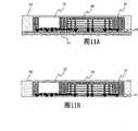
图10A-10C为顺序地显示根据第二实施例的电子器件的制造方法的剖面图;10A-10C are sectional views sequentially showing a method of manufacturing an electronic device according to a second embodiment;
图11A和11B为顺序地显示根据第二实施例的电子器件的制造方法的剖面图;11A and 11B are sectional views sequentially showing a method of manufacturing an electronic device according to a second embodiment;
图12A和12B为顺序地显示根据第二实施例的电子器件的制造方法的剖面图;12A and 12B are sectional views sequentially showing a method of manufacturing an electronic device according to a second embodiment;
图13为根据本发明第三实施例的电子器件的剖面图;13 is a cross-sectional view of an electronic device according to a third embodiment of the present invention;
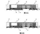
图14A和14B为顺序地显示根据第三实施例的电子器件的制造方法的剖面图;14A and 14B are sectional views sequentially showing a method of manufacturing an electronic device according to a third embodiment;
图15为用于说明实施例的变化的剖面图;Fig. 15 is a sectional view for explaining a variation of the embodiment;
图16为用于说明实施例的另一个变化的剖面图;Fig. 16 is a cross-sectional view illustrating another variation of the embodiment;
图17为用于说明实施例的还另一个变化的剖面图;以及FIG. 17 is a sectional view for explaining yet another variation of the embodiment; and
图18为用于说明实施例的还以另一个变化的剖面图。Fig. 18 is a sectional view for explaining yet another variation of the embodiment.
具体实施方式Detailed ways
下面将参照说明性实施例来描述本发明。本领域内的技术人员可以认识到,通过使用本发明的教导可以实现许多替换实施例,并且本发明并不限于仅用于说明目的的实施例。The invention will be described below with reference to illustrative embodiments. Those skilled in the art will recognize that many alternative embodiments can be accomplished by using the teachings of the present invention and that the invention is not limited to the embodiments described for explanatory purposes only.
在下文中,将参照附图来详细地描述根据本发明的电子器件及其制造方法的实施例。在全部附图中,相同的数字来表示相同的部件,并且不会重复对它们的描述。Hereinafter, embodiments of an electronic device and a manufacturing method thereof according to the present invention will be described in detail with reference to the accompanying drawings. Throughout the drawings, the same numerals denote the same components, and their descriptions will not be repeated.
第一实施例first embodiment
图1为根据本发明第一实施例的电子器件的剖面图。该电子器件1包括互连层10(第一互连层)以及互连层20(第二互连层)。FIG. 1 is a cross-sectional view of an electronic device according to a first embodiment of the present invention. The
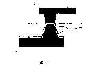
该互连层10包括通路插塞12(第一导电插塞),绝缘树脂14以及导体互连16。该通路插塞12配备在该绝缘树脂14上。如图1中可以清晰的看到,该通路插塞12为锥形,它的直径朝着互连层20的方向逐渐减小。因此,该互连层20一侧上的通路插塞12的端面的面积小于相对端面的面积,即将在后面描述的IC芯片32,36一侧上的端面。该通路插塞12暴露在与该互连层20相对的互连层10的表面上。The
该通路插塞12的导体可以为例如铜(Cu),镍(Ni),金(Au)或银(Ag)。该绝缘树脂14可以由聚酰亚胺树脂、聚苯并唑(下文中称PBO,polybenzoxazole)树脂,苯并环丁烯(BCB)树脂,芴环树脂(cardo resin,芴环聚合物,cardo polymer)或环氧树脂构成。该聚酰亚胺树脂可以为感光的或者非感光的。在该绝缘树脂14上配备有导体互连16,以便于与通路插塞12相连。The conductor of the
在该互连层10的上表面(第一表面)上安装有IC芯片32,36(电子元件)。该IC芯片32,36分别通过凸块33,37倒装连接至导体互连16。在该IC芯片32与互连层10之间的间隙中装载有下填充树脂34。同样地,在IC芯片36与互连层10之间的间隙中填充有下填充树脂38。多个IC芯片36被配置为彼此堆叠在一块。该IC芯片32和IC芯片36可以分别为例如CPU和堆叠的存储器。该堆叠的存储器由彼此电连接的三维堆叠的IC芯片(存储器)构成。On the upper surface (first surface) of this
该IC芯片32,36上覆盖有互连层10上配备的封装树脂52。更详细地,IC芯片32的侧面以及IC芯片36的侧面和上表面覆盖有封装树脂52。The IC chips 32 , 36 are covered with the
该互连层10的下表面(第二表面)上配备有互连层20。在平面图中,该互连层20的面积大于互连层10,并且延伸至互连层10的外部区域。换句话说,该互连层20从互连层10向外伸出。An
该互连层20包括通路插塞22(第二导电插塞)以及绝缘树脂24。该通路插塞22配备在绝缘树脂24中。每个通路插塞22与通路插塞12相连。从图1清楚地看出,该通路插塞22具有锥形形状,它的直径朝着互连层10的方向逐渐减小。因此,该互连层10一侧上通路插塞22的端面的面积小于相对的端面,即将在随后描述的焊球60侧上的端面。该通路插塞22的导体可以为例如铜(Cu),镍(Ni),金(Au)或银(Ag)。该绝缘树脂24可以由例如环氧树脂构成。由互连层10和互连层20构成的互连结构在电子器件1中起到插入物的作用。The
形成该互连层10的绝缘树脂14的热分解温度高于形成互连层20的绝缘树脂24的热分解温度。在采用PBO树脂作为绝缘树脂14的情况下,该热分解温度为例如540℃。在采用环氧树脂作为绝缘树脂24的情况下,该热分解温度为例如310℃。这里的热分解温度是指在该温度下,以每分钟10℃的加热速率用热天平(thermo balance)测得该树脂的重量降低5%。这里,在采用相同类型的树脂(例如环氧树脂)作为绝缘树脂14,24的情况下,前者应该具有比后者更高的热分解温度。The thermal decomposition temperature of the insulating
在延伸出该互连层10的互连层20的区域上安装有IC芯片42和无源元件44,作为第二电子元件。该无源元件44可以为电容器,例如去耦电容器。该IC芯片42被封装树脂54覆盖。该无源元件44被树脂56覆盖,其中该树脂56配备在互连层20向外延伸的区域上。该树脂56可以是与封装树脂54相同的树脂,或者不同的树脂。An
该互连层20具有多层互连结构,包括在多个层中形成的导体互连26,以及与不同层的导体互连26相连的通路插塞28。该焊球60与最低层的导体互连26相连。该焊球60部分地埋置在阻焊剂62中。该焊球60起到电子器件1的外部连接端的作用。The
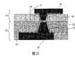
参看图2,下面将描述互连层10与互连层20之间的界面周围结构的例子。在该例中,配备有粘接金属层72(第二粘接金属层),用以覆盖该通路插塞22。该粘接金属层72与通路插塞22上的通路插塞12接触。此外,在与通路插塞12接触的导体互连16的表面上配备有粘接金属层74(第一粘接金属层)。Referring to FIG. 2, an example of the structure around the interface between the
优选地,该粘接金属层72,74由含有Ti(例如,Ti,TiN或TiW膜)的膜,或者Cr膜构成。Preferably, the bonding metal layers 72, 74 are formed of a film containing Ti (for example, a Ti, TiN or TiW film), or a Cr film.
参看图3A-7,下面将描述制造该电子器件1的方法,作为根据本发明制造电子器件的方法的第一实施例。在开始详细描述之前,参照图3A-3E来描述该制造方法的概要。首先,如图3A所示,在支撑衬底90上形成互连层10(形成第一互连层的步骤)。该支撑衬底90可以为硅衬底,陶瓷衬底,玻璃衬底或者金属衬底。Referring to FIGS. 3A-7 , a method of manufacturing the
接着如图3B所示,将IC芯片32,36安装在互连层10上(安装电子元件的步骤)。如图3C所示,进一步在互连层10上形成封装树脂52,以便于覆盖该IC芯片32,36(形成封装树脂的步骤)。接着,如图3D中所示,去除该支撑衬底90(去除支撑衬底的步骤)。之后,如图3E所示,在互连层10的下表面上形成互连层20(形成第二互连层的步骤)。最后,虽然图中未示出,形成焊球60,从而获得了如图1中所示电子器件1。Next, as shown in FIG. 3B, IC chips 32, 36 are mounted on the interconnection layer 10 (step of mounting electronic components). As shown in FIG. 3C, an
现在参看图4A-7来更详细地描述该制造方法。首先,在支撑衬底90上配备绝缘树脂14,并在该绝缘树脂14中形成通路插塞12。接着,在该绝缘树脂14上形成导体互连16(图4A)。接着,在该导体互连16上倒装安装IC芯片32,36(图4B)。之后,在该互连层10上配备封装树脂52,以便覆盖该IC芯片32,36。可以通过例如模塑、印刷或者罐封(potting)来形成封装树脂52(图5A)。接着,去除该支撑衬底90,以便暴露出该通路插塞12。The fabrication method is now described in more detail with reference to FIGS. 4A-7. First, insulating
在该互连层10上初始配备有支撑衬底,而在互连层10的下表面上形成了绝缘树脂24,以便延伸至该互连层10的外部区域。该绝缘树脂24可以由绝缘膜构成。接着,在从该互连层10向外延伸的绝缘树脂24的区域上实现IC芯片42和无源元件44。接着,形成封装树脂54,以便覆盖该IC芯片42(图6A)。另外,还配备了树脂56,用于填充在从该互连层10向外延伸的绝缘树脂24的区域上剩余的间隙。这样,该无源元件44就被树脂56覆盖(图6B)。A supporting substrate is initially provided on the
接着,在绝缘树脂24中形成通路插塞22,以便于与通路插塞12相连。随后在绝缘树脂24上形成内嵌互连层。形成过程的例子包括在例如环氧树脂的绝缘树脂层中通过半加成工艺形成导体互连26以及通过激光工艺形成通路插塞28。通过该工艺,就得到了互连层20(图7)。之后,通过形成阻焊剂62和焊球60,就能够得到如图1中所示的电子器件1。这里,实现提前单独形成的多层互连结构可以被粘接至该互连层10的下表面,从而形成互连层20。Next, the via
从上面的描述中可以理解的是,根据相关附图中的方向,该互连层10,20的内嵌方向分别为向上和向下。在这种结构下,如上所述的,通路插塞12在IC芯片32,36侧上具有比互连层侧上更大的端面,以及通路插塞22在焊球60侧具有比互连层10侧更大的端面。It can be understood from the above description that, according to the directions in the related drawings, the embedding directions of the interconnection layers 10 and 20 are upward and downward respectively. Under this structure, as described above, the via
该实施例具备如下有益效果。通过上面的制造方法,在支撑衬底90上形成其上安装有IC芯片32,36的互连层10,并且接着在形成互连层20之前去除该支撑衬底90。这种结构消除了如下限制,即无法采用热分解温度比绝缘树脂14的热分解温度更低的树脂来作为绝缘树脂24。因此,该方法允许采用适于微处理的树脂来作为绝缘树脂14,同时采用相对较便宜的树脂来作为绝缘树脂24。这样,上述实施例提供了一种制造电子器件1的方法,该方法能够实现互连层10与IC芯片32、36之间的精确连接,而成本很低。This embodiment has the following beneficial effects. By the above manufacturing method, the
此外,在去除该支撑衬底90时会暴露出该通路插塞12(参看图5B)。因此,在去除该支撑衬底90之后进行电检查时该通路插塞12可以被用作端子,其有利于在较早的阶段在工艺中检测到电子器件中的故障,如果存在的话。In addition, the via
该互连层20延伸至互连层10的外部区域。该结构允许确保用于配备焊球60(即,互连层20的下表面)的足够的区域,同时保持该互连层10尽可能的小。因此,可以很容易地将该电子器件1安装在另一个电子器件或母板上,而不会导致成本增加。相反,在互连层10和互连层20面积相同的情况下,延伸该互连层20促进安装过程会不可避免地导致互连层10面积的增加。由于采用了适于微处理的相对昂贵的树脂来构成互连层10,因此这就很自然地导致增加电子器件1的制造成本。另一方面,在试图降低成本时降低互连层10的面积就会迫使该互连层20的面积更小,这样就降低了安装便利性。这样,上面实施例就消除了这个矛盾并且同时实现了低成本和安装的便利性。The
由于在其上形成有导体互连16的图案的支撑衬底90的刚性结构,因此能够以足够精致的图案形成导体互连16。此外,由于在刚性的支撑衬底90上连接了该互连层10和IC芯片32,36,因此能够通过凸块以精确的间距将互连层10和IC芯片32,36连接在一块。这有助于降低互连层的数量,以及减小IC芯片32,36的尺寸。Due to the rigid structure of the
进一步,由于在去除该支撑衬底90之后形成互连层20,因此可以形成比绝缘树脂14更厚的绝缘树脂24,用于形成互连层20。因此,该绝缘树脂24获得了更高的应力消除性能,而这导致了该电子器件1更高的可靠性。Further, since the
在形成第二互连层的步骤中,采用热分解温度比在形成第一互连层10的步骤中采用的、用于形成互连层10的绝缘树脂14的热分解温度更低的树脂作为用于形成互连层20的绝缘树脂24。这种结构允许在互连层10上适当地形成互连层20。In the step of forming the second interconnection layer, a resin having a thermal decomposition temperature lower than that of the insulating
在该电子器件1中,可以采用热分解温度比用于形成互连层10的绝缘树脂14的热分解温度更低的树脂作为用于形成互连层20的绝缘树脂24。因此,可以采用适于微处理的树脂作为绝缘树脂14,同时采用相对便宜的树脂作为绝缘树脂24。这样,该电子器件1能够实现互连层10和IC芯片32,36之间的精确连接,而成本很低。In this
在该电子器件1中,互连层10和互连层20彼此直接接触,而在它们之间没有配备芯层。一般地,芯层中形成的通路插塞比普通互连层中形成的通路插塞更难微型化(micronize),因此,配备该芯层就从整体上妨碍了该电子器件的微型化。没有包括该芯层的电子器件1不受这些缺点的影响。In this
配备了该封装树脂52,以便于覆盖该IC芯片32,36。该结构允许在去除支撑衬底90之后保持该互连层的形状。因此,能够获得同面性很高的焊球60。特别是在该实施例中,还在从互连层10向外延伸的互连层20的区域上配备有树脂56,而这就增强了上述效果。The encapsulating
与绝缘衬底相比,采用硅衬底作为支撑衬底90使得热膨胀的效果最小化。因此,该结构进一步促进了互连层10与IC芯片32,36之间连接的微型化。Using a silicon substrate as the
采用聚酰亚胺树脂,PBO树脂,,BCB树脂,芴环(cardo)树脂作为绝缘树脂14允许该绝缘树脂14具有适于微处理的属性。采用环氧树脂作为绝缘树脂24允许以很低成本形成绝缘树脂24。Using polyimide resin, PBO resin, BCB resin, cardo resin as the insulating
配备了粘接金属层72,以便于覆盖该通路插塞22(参看图2)。该粘接金属层72用于确保通路插塞22与绝缘树脂24之间的牢固粘接。此外,在与通路插塞12接触的导体互连16的表面上配备了粘接金属层74(参看图2)。该粘接金属层74也确保了导体互连16与绝缘树脂14之间的牢固粘接。该粘接金属层75确保了通路插塞28与绝缘树脂24之间的牢固粘接。该牢固粘接很自然地导致了提高电子器件1的可靠性。当该粘接金属层72,74含有Ti,或者由Cr构成时,该粘接金属层72,74能够实现与树脂的显著牢固粘接。An
该IC芯片42和无源元件44被安装在从该互连层10向外延伸的互连层20的区域上。该结构能够进一步增强该电子器件1的功能和性能。The
第二实施例second embodiment
图8为根据本发明第二实施例的电子器件的剖面图。该电子器件2包括互连层10(第一互连层),以及互连层80(第二互连层)。该互连层10具有与参照图1中所述类似的结构。8 is a cross-sectional view of an electronic device according to a second embodiment of the present invention. The electronic device 2 includes an interconnection layer 10 (first interconnection layer), and an interconnection layer 80 (second interconnection layer). The
该互连层80配备在互连层10的下表面上,以便于延伸至该互连层10的外部区域。该互连层80包括阻焊剂84,以及在该阻焊剂84中形成的导体互连86。该导体互连层86与通路插塞12相连。该阻焊剂84由热分解温度比绝缘树脂14的热分解温度更低的树脂构成。该互连层80包括通路插塞82(第二导电插塞),其与导体互连层86相连。该通路插塞82对应于部分焊球60,更具体地为埋置在阻焊剂84中的一部分。如图8中可以清晰看到的,该通路插塞82为锥形,并且它的直径朝着互连层10逐步减小。因此,该互连层10一侧上的通路插塞82的端面的面积小于相对的端面的面积。The
此外,IC芯片92倒装安装在该互连层10的下表面上。换句话说,该IC芯片92通过凸块93与下表面相连,并且用下填充树脂94来填充该互连层10与IC芯片92之间的间隙。在从互连层10向外延伸的互连层80的区域上配备有树脂56。在该实施例中,该树脂56同时覆盖了该封装树脂52的侧面和顶面。Furthermore, an
参看图9A-12B,下面将描述制造该电子器件2的方法,作为根据本发明的制造电子器件的方法的第二实施例。首先,在支撑衬底90上形成绝缘树脂14,通路插塞12,以及导体互连16(图9A)。接着,在导体互连16上倒装安装IC芯片32,36(图9B)。Referring to FIGS. 9A-12B , a method of manufacturing the electronic device 2 will be described below as a second embodiment of the method of manufacturing an electronic device according to the present invention. First, insulating
之后,在互连层10上形成封装树脂52,以便于覆盖该IC芯片32,36(图10A)。接着,去除该支撑衬底90,以便于暴露出该通路插塞12(图10B)。在该互连层10的下表面上配备有支撑片91,以便于从该互连层10向外延伸(图10C)。Thereafter, an
接着,在该互连层10外部的支撑片91的区域上配备有树脂56,以便于覆盖该封装树脂52(图11A)。之后,该支撑片91被剥去(图11B)。接着,在该互连层10的下表面上形成导体互连86,以便于与通路插塞12相连。之后,配备了阻焊剂84,以便于覆盖该导体互连86。对该阻焊剂84进行图案化,以便于形成开口,其中在该开口处将配备焊球60并且将要安装IC芯片92(图12A)。在这一阶段,获得了互连层80。接着,将IC芯片92倒装安装在该互连层10的下表面上(图12B)。之后通过形成焊球60,就能够获得如图8中所示的电子器件2。Next, a
除了第一实施例提供的有益效果以外,该实施例还具备如下有益效果。由于该阻焊剂84被用作形成互连层80的树脂,因此能够进一步降低该电子器件2的成本。此外,该电子元件(IC芯片92)不仅实现在互连层10的上表面上,而且还实现在它的下表面上。该结构进一步增强了该电子器件2的功能和性能。In addition to the beneficial effects provided by the first embodiment, this embodiment also has the following beneficial effects. Since the solder resist 84 is used as the resin forming the
第三实施例third embodiment
图13为根据本发明第三实施例的电子器件的剖面图。该电子器件3包括互连层10,以及互连层80。该电子器件3与图8中所示的电子器件2的不同之处在于该互连层80具有多层互连结构。在该实施例中,该互连层80包括在互连层10的下表面上配备的绝缘树脂84a,以及在该绝缘树脂84a上配备的阻焊剂84b。13 is a cross-sectional view of an electronic device according to a third embodiment of the present invention. The electronic device 3 includes an
根据该实施例的互连层80包括在多层中配备的导体互连86,以及与该导体互连86相连的通路插塞83(第二导电插塞)。从图13中可以清晰的看到,该通路插塞83为锥形,并且它的直径朝着互连层10逐步减小。因此,该互连层10一侧上的通路插塞83的端面的面积小于相对的端面的面积。进一步,虽然在该电子器件2中该凸起93直接与通路插塞12相连,但是在该电子器件3中该凸起93通过导体互连86(以及通路插塞83)与通路插塞12相连。该电子器件3其余部分的结构与电子器件2类似。The
参看图14A和14B,下面将描述制造该电子器件3的方法,作为根据本发明的制造电子器件的方法的第三实施例。首先,通过参照图9A-11B描述的过程来形成如图11B中所示的结构。Referring to FIGS. 14A and 14B, a method of manufacturing the electronic device 3 will be described below as a third embodiment of the method of manufacturing an electronic device according to the present invention. First, a structure as shown in FIG. 11B is formed through the process described with reference to FIGS. 9A-11B.
接着,在互连层10的下表面上形成导体互连86的第一层,以便于与通路插塞12相连。接着,配备了绝缘树脂84a,以便于覆盖该导体互连86。进一步,在该绝缘树脂84a中形成通路插塞83,以便于与该导体互连86相连。接着,在该绝缘树脂84a中形成导体互连86的第二层,以便于与该通路插塞83相连。之后,配备了阻焊剂84b,以便于覆盖该导体互连86的第二层。Next, a first layer of
接着,对该阻焊剂84b进行图案化,从而在将要形成焊球60以及要实现IC芯片92的位置上形成开口(图14A)。在该阶段,得到了互连层80。之后,将IC芯片92倒装安装在绝缘树脂84a上(图14B)。之后,当形成焊球60时,就能够得到如图13中所示的电子器件3。该实施例提供了与第二实施例相同的有益效果。Next, this solder resist 84b is patterned to form openings at positions where
根据本发明的电子器件及其制造方法并不仅限于上面的实施例,但是可以进行各种修改。虽然上面的实施例中,为了引用一些例子,采用了IC芯片作为将要安装在互连结构的上表面或下表面上的电子元件的例子,其中该互连结构包括第一和第二互连层,但是该电子元件也可以为无源元件,例如电容器。此外,该电子器件并不是必须包括电子元件。The electronic device and its manufacturing method according to the present invention are not limited to the above embodiments, but various modifications can be made. Although in the above embodiments, an IC chip is used as an example of an electronic component to be mounted on an upper surface or a lower surface of an interconnection structure including first and second interconnection layers in order to cite some examples , but the electronic component can also be a passive component, such as a capacitor. Furthermore, the electronic device does not necessarily include electronic components.
虽然在根据实施例的电子器件中配备了焊球,但是配备焊球并不是强制性的。在没有配备焊球的情况下,该导体互连的岛部分起到外部电极端的作用。以参看图1中所示的电子器件1为例,该与焊球60接触的部分导体互连26相当于岛部分。Although the solder balls are provided in the electronic device according to the embodiment, it is not mandatory to provide the solder balls. In the case where no solder balls are provided, the island portion of the conductor interconnection functions as an external electrode terminal. Taking the
在上面的实施例中,该第二互连层延伸至第一互连层的外部区域。但是该结构不是强制性的,而是该第一和第二互连层可以在平面图上具有相同的面积。In the above embodiments, the second interconnection layer extends to an outer region of the first interconnection layer. But the structure is not mandatory, but the first and second interconnection layers may have the same area in plan view.
也可以按照各种方式来修改第一和第二互连层之间的分界面周围的结构,而不仅限于图2中所示的结构。例如,如图15中所示,配备了粘接金属层76,以便于覆盖该通路插塞12,即,如图2,电子器件1的放大部分图。该粘接金属层76在通路插塞12的端面处与粘接金属层72接触。这样,提供该粘接金属层76就确保了通路插塞12与绝缘树脂14之间的牢固粘接。该粘接金属层76可以由与粘接金属层72,74中采用的膜类似的膜构成。The structure around the interface between the first and second interconnection layers can also be modified in various ways, not limited to the structure shown in FIG. 2 . For example, as shown in FIG. 15 , an
此外,在上面实施例中,该导电材料被载入到整个通孔中,用以形成该通路插塞。但是,该通孔可以部分地填充导电材料。图16描述了如图2中所示的结构,但是其中通过部分地填充相关的通孔来形成通路插塞22。这里,虽然导电材料部分地填充该通孔,但是该通路插塞端面的面积被限定为被该端面的外圆周包围的区域的面积。因此,只要通孔的大小相同,那么端面的面积就是相同的,而与该导电材料是全部还是部分填充该通孔无关。Furthermore, in the above embodiments, the conductive material is loaded into the entire via hole to form the via plug. However, the via may be partially filled with conductive material. FIG. 16 depicts the structure as shown in FIG. 2 , but in which via plugs 22 are formed by partially filling the associated via holes. Here, although the conductive material partially fills the through hole, the area of the end face of the via plug is limited to the area of a region surrounded by the outer circumference of the end face. Therefore, as long as the size of the via is the same, the area of the end face is the same regardless of whether the conductive material completely or partially fills the via.
进一步,如图17和18所示,可以配备粘接金属层73,以便于覆盖该通路插塞83(参看图13)。该粘接金属层73在通路插塞83的末端部分处与导体互连86接触。这样,配备了粘接金属层73就可以确保通路插塞83与绝缘树脂84a之间的牢固粘接。此外,在这些图中,在与通路插塞12接触的导体互连86的表面上配备了粘接金属层78。这样,配备了粘接金属层78就可以确保通导体互连86与绝缘树脂14之间的牢固粘接。该粘接金属层73,78可以由与粘接金属层72,74中采用的膜类似的膜构成。Further, as shown in FIGS. 17 and 18, an
很清楚的是,本发明不仅限于上面的实施例,并且可以在不脱离本发明的精神和范畴的情况下进行修改和改变。It is clear that the present invention is not limited to the above embodiments, and that modifications and changes can be made without departing from the spirit and scope of the present invention.
Claims (20)
Translated fromChineseApplications Claiming Priority (2)
| Application Number | Priority Date | Filing Date | Title |
|---|---|---|---|
| JP2006271156 | 2006-10-02 | ||
| JP2006271156AJP2008091639A (en) | 2006-10-02 | 2006-10-02 | Electronic equipment, and manufacturing method thereof |
Publications (2)
| Publication Number | Publication Date |
|---|---|
| CN101159238Atrue CN101159238A (en) | 2008-04-09 |
| CN100587929C CN100587929C (en) | 2010-02-03 |
Family
ID=39260340
Family Applications (1)
| Application Number | Title | Priority Date | Filing Date |
|---|---|---|---|
| CN200710149970AExpired - Fee RelatedCN100587929C (en) | 2006-10-02 | 2007-10-08 | Electronic device and manufacturing method thereof |
Country Status (3)
| Country | Link |
|---|---|
| US (1) | US7928001B2 (en) |
| JP (1) | JP2008091639A (en) |
| CN (1) | CN100587929C (en) |
Cited By (1)
| Publication number | Priority date | Publication date | Assignee | Title |
|---|---|---|---|---|
| CN111211107A (en)* | 2018-11-21 | 2020-05-29 | 三星电子株式会社 | Semiconductor package |
Families Citing this family (18)
| Publication number | Priority date | Publication date | Assignee | Title |
|---|---|---|---|---|
| JP5262552B2 (en)* | 2008-10-14 | 2013-08-14 | 富士電機株式会社 | Semiconductor device manufacturing method and semiconductor device |
| US7741148B1 (en)* | 2008-12-10 | 2010-06-22 | Stats Chippac, Ltd. | Semiconductor device and method of forming an interconnect structure for 3-D devices using encapsulant for structural support |
| US20110156261A1 (en)* | 2009-03-24 | 2011-06-30 | Christopher James Kapusta | Integrated circuit package and method of making same |
| US9299661B2 (en)* | 2009-03-24 | 2016-03-29 | General Electric Company | Integrated circuit package and method of making same |
| JP5147779B2 (en) | 2009-04-16 | 2013-02-20 | 新光電気工業株式会社 | Wiring board manufacturing method and semiconductor package manufacturing method |
| JP5581064B2 (en)* | 2010-01-14 | 2014-08-27 | パナソニック株式会社 | Semiconductor device |
| US8546922B2 (en)* | 2010-09-30 | 2013-10-01 | Ibiden Co., Ltd. | Wiring board |
| US8508037B2 (en)* | 2010-12-07 | 2013-08-13 | Intel Corporation | Bumpless build-up layer and laminated core hybrid structures and methods of assembling same |
| KR101411813B1 (en) | 2012-11-09 | 2014-06-27 | 앰코 테크놀로지 코리아 주식회사 | Semiconductor device and manufacturing method thereof |
| US10418298B2 (en)* | 2013-09-24 | 2019-09-17 | STATS ChipPAC Pte. Ltd. | Semiconductor device and method of forming dual fan-out semiconductor package |
| US10345571B2 (en) | 2014-01-30 | 2019-07-09 | Karl Storz Endovision, Inc. | Intelligent light source |
| US9583460B2 (en)* | 2014-02-14 | 2017-02-28 | Qualcomm Incorporated | Integrated device comprising stacked dies on redistribution layers |
| KR20150104467A (en)* | 2014-03-05 | 2015-09-15 | 앰코 테크놀로지 코리아 주식회사 | Manufacturing method of semiconductor device and semiconductor device thereof |
| US9418877B2 (en)* | 2014-05-05 | 2016-08-16 | Qualcomm Incorporated | Integrated device comprising high density interconnects in inorganic layers and redistribution layers in organic layers |
| US9627285B2 (en) | 2014-07-25 | 2017-04-18 | Dyi-chung Hu | Package substrate |
| DE102014118214B4 (en)* | 2014-12-09 | 2024-02-22 | Snaptrack, Inc. | Easily manufactured electrical component and method for producing an electrical component |
| US10283428B2 (en)* | 2017-06-30 | 2019-05-07 | Taiwan Semiconductor Manufacturing Co., Ltd. | Semiconductor package and method manufacturing the same |
| US11139268B2 (en)* | 2019-08-06 | 2021-10-05 | Advanced Semiconductor Engineering, Inc. | Semiconductor package structure and method of manufacturing the same |
Family Cites Families (43)
| Publication number | Priority date | Publication date | Assignee | Title |
|---|---|---|---|---|
| JPS577147A (en) | 1980-06-17 | 1982-01-14 | Citizen Watch Co Ltd | Mounting construction of semiconductor device |
| JPS598137A (en)* | 1982-07-06 | 1984-01-17 | Fuji Photo Film Co Ltd | Magnetic recording medium |
| US4788097A (en)* | 1986-02-12 | 1988-11-29 | Fuji Photo Film Co., Ltd. | Information recording medium |
| US5353498A (en)* | 1993-02-08 | 1994-10-11 | General Electric Company | Method for fabricating an integrated circuit module |
| JP2842378B2 (en) | 1996-05-31 | 1999-01-06 | 日本電気株式会社 | High-density mounting structure for electronic circuit boards |
| JPH11126978A (en) | 1997-10-24 | 1999-05-11 | Kyocera Corp | Multilayer wiring board |
| JP3378505B2 (en)* | 1998-06-23 | 2003-02-17 | 株式会社東芝 | Semiconductor device and manufacturing method thereof |
| JP3949849B2 (en)* | 1999-07-19 | 2007-07-25 | 日東電工株式会社 | Manufacturing method of interposer for chip size package and interposer for chip size package |
| JP2001044280A (en)* | 1999-07-27 | 2001-02-16 | Matsushita Electronics Industry Corp | Multilayer wiring structure and manufacture thereof |
| JP2001044589A (en)* | 1999-07-30 | 2001-02-16 | Nitto Denko Corp | Circuit board |
| JP2001053413A (en) | 1999-08-16 | 2001-02-23 | Sony Corp | Substrate incorporating electronic parts, multilayered substrate incorporating electronic parts, and their manufacture |
| JP3973340B2 (en)* | 1999-10-05 | 2007-09-12 | Necエレクトロニクス株式会社 | Semiconductor device, wiring board, and manufacturing method thereof |
| JP3677429B2 (en)* | 2000-03-09 | 2005-08-03 | Necエレクトロニクス株式会社 | Method of manufacturing flip chip type semiconductor device |
| JP2001267747A (en)* | 2000-03-22 | 2001-09-28 | Nitto Denko Corp | Method for manufacturing multilayer circuit board |
| US6370012B1 (en)* | 2000-08-30 | 2002-04-09 | International Business Machines Corporation | Capacitor laminate for use in printed circuit board and as an interconnector |
| JP4344101B2 (en)* | 2001-02-14 | 2009-10-14 | Okiセミコンダクタ株式会社 | Wiring structure |
| JP4087080B2 (en)* | 2001-05-17 | 2008-05-14 | 株式会社日立製作所 | Wiring board manufacturing method and multichip module manufacturing method |
| US6692818B2 (en)* | 2001-06-07 | 2004-02-17 | Matsushita Electric Industrial Co., Ltd. | Method for manufacturing circuit board and circuit board and power conversion module using the same |
| JP3861669B2 (en) | 2001-11-22 | 2006-12-20 | ソニー株式会社 | Manufacturing method of multichip circuit module |
| JP2003163323A (en)* | 2001-11-27 | 2003-06-06 | Sony Corp | Circuit module and manufacturing method thereof |
| JP3665935B2 (en)* | 2001-12-13 | 2005-06-29 | 三星電子株式会社 | Insulating film forming method and semiconductor device |
| JP3773896B2 (en) | 2002-02-15 | 2006-05-10 | Necエレクトロニクス株式会社 | Manufacturing method of semiconductor device |
| SG115455A1 (en)* | 2002-03-04 | 2005-10-28 | Micron Technology Inc | Methods for assembly and packaging of flip chip configured dice with interposer |
| JPWO2003076515A1 (en)* | 2002-03-08 | 2005-07-07 | 株式会社カネカ | Thermosetting resin composition, laminated body using the same, and circuit board |
| JP2003304065A (en)* | 2002-04-08 | 2003-10-24 | Sony Corp | Circuit board device, its manufacturing method, semiconductor device, and method of manufacturing the same |
| JP2003315775A (en)* | 2002-04-26 | 2003-11-06 | Hitachi Displays Ltd | Liquid crystal display device and method of manufacturing the same |
| JP2004039867A (en)* | 2002-07-03 | 2004-02-05 | Sony Corp | Multilayer wiring circuit module and its manufacturing method |
| JP4023285B2 (en)* | 2002-10-24 | 2007-12-19 | ソニー株式会社 | Optical / electrical wiring mixed hybrid circuit board and manufacturing method thereof, and optical / electrical wiring mixed hybrid circuit module and manufacturing method thereof |
| US6949456B2 (en)* | 2002-10-31 | 2005-09-27 | Asm Japan K.K. | Method for manufacturing semiconductor device having porous structure with air-gaps |
| US6943121B2 (en)* | 2002-11-21 | 2005-09-13 | Intel Corporation | Selectively converted inter-layer dielectric |
| JP4066848B2 (en)* | 2003-02-28 | 2008-03-26 | 株式会社トッパンNecサーキットソリューションズ | Manufacturing method of multilayer printed wiring board |
| KR100499174B1 (en)* | 2003-06-17 | 2005-07-01 | 삼성전자주식회사 | Image device |
| KR20060098432A (en) | 2003-09-24 | 2006-09-18 | 코닌클리즈케 필립스 일렉트로닉스 엔.브이. | Semiconductor device, identification label, information transfer medium and semiconductor device manufacturing method |
| US7659633B2 (en)* | 2004-11-10 | 2010-02-09 | Stats Chippac, Ltd. | Solder joint flip chip interconnection having relief structure |
| JP4204989B2 (en)* | 2004-01-30 | 2009-01-07 | 新光電気工業株式会社 | Semiconductor device and manufacturing method thereof |
| JP3961537B2 (en)* | 2004-07-07 | 2007-08-22 | 日本電気株式会社 | Manufacturing method of semiconductor mounting wiring board and manufacturing method of semiconductor package |
| CN1819179A (en)* | 2005-02-10 | 2006-08-16 | 恩益禧电子股份有限公司 | Semiconductor device and method of manufacturing the same |
| JP4790297B2 (en)* | 2005-04-06 | 2011-10-12 | ルネサスエレクトロニクス株式会社 | Semiconductor device and manufacturing method thereof |
| JP4787559B2 (en)* | 2005-07-26 | 2011-10-05 | ルネサスエレクトロニクス株式会社 | Semiconductor device and manufacturing method thereof |
| JP4671829B2 (en)* | 2005-09-30 | 2011-04-20 | 富士通株式会社 | Interposer and method for manufacturing electronic device |
| JP5103724B2 (en)* | 2005-09-30 | 2012-12-19 | 富士通株式会社 | Manufacturing method of interposer |
| JP2007266073A (en)* | 2006-03-27 | 2007-10-11 | Toshiba Corp | Semiconductor device and manufacturing method thereof |
| JP2008091638A (en)* | 2006-10-02 | 2008-04-17 | Nec Electronics Corp | Electronic equipment, and manufacturing method thereof |
- 2006
- 2006-10-02JPJP2006271156Apatent/JP2008091639A/enactivePending
- 2007
- 2007-10-02USUS11/865,750patent/US7928001B2/enactiveActive
- 2007-10-08CNCN200710149970Apatent/CN100587929C/ennot_activeExpired - Fee Related
Cited By (4)
| Publication number | Priority date | Publication date | Assignee | Title |
|---|---|---|---|---|
| CN111211107A (en)* | 2018-11-21 | 2020-05-29 | 三星电子株式会社 | Semiconductor package |
| US11881467B2 (en) | 2018-11-21 | 2024-01-23 | Samsung Electronics Co., Ltd. | Semiconductor package |
| CN111211107B (en)* | 2018-11-21 | 2024-03-12 | 三星电子株式会社 | Semiconductor packages |
| US12308336B2 (en) | 2018-11-21 | 2025-05-20 | Samsung Electronics Co., Ltd. | Semiconductor package |
Also Published As
| Publication number | Publication date |
|---|---|
| CN100587929C (en) | 2010-02-03 |
| US7928001B2 (en) | 2011-04-19 |
| US20080079164A1 (en) | 2008-04-03 |
| JP2008091639A (en) | 2008-04-17 |
Similar Documents
| Publication | Publication Date | Title |
|---|---|---|
| CN101604682B (en) | Electronic device and method of manufacturing the same | |
| CN101159238A (en) | Electronic device and manufacturing method thereof | |
| US10008468B2 (en) | Packaged microelectronic devices and methods for manufacturing packaged microelectronic devices | |
| KR100800478B1 (en) | Multilayer semiconductor package and manufacturing method thereof | |
| US9406602B2 (en) | Electronic device | |
| JP4790297B2 (en) | Semiconductor device and manufacturing method thereof | |
| KR100609011B1 (en) | Wafer level module and manufacturing method thereof | |
| JP2018137474A (en) | Electronic equipment | |
| JP7197448B2 (en) | electronic device | |
| JP5607692B2 (en) | Electronic equipment | |
| JP6335265B2 (en) | Electronic equipment | |
| JP2014096609A (en) | Electronic apparatus | |
| JP2019036742A (en) | Electronic equipment | |
| JP2018050077A (en) | Electronic apparatus | |
| CN112992840A (en) | Package structure and method for manufacturing the same | |
| US20080179727A1 (en) | Semiconductor packages having immunity against void due to adhesive material and methods of fabricating the same | |
| JP2015146467A (en) | Electronic apparatus |
Legal Events
| Date | Code | Title | Description |
|---|---|---|---|
| C06 | Publication | ||
| PB01 | Publication | ||
| C10 | Entry into substantive examination | ||
| SE01 | Entry into force of request for substantive examination | ||
| C14 | Grant of patent or utility model | ||
| GR01 | Patent grant | ||
| C56 | Change in the name or address of the patentee | Owner name:RENESAS ELECTRONICS CORPORATION Free format text:FORMER NAME: NEC CORP. | |
| CP01 | Change in the name or title of a patent holder | Address after:Kanagawa, Japan Patentee after:Renesas Electronics Corporation Address before:Kanagawa, Japan Patentee before:NEC Corp. | |
| C17 | Cessation of patent right | ||
| CF01 | Termination of patent right due to non-payment of annual fee | Granted publication date:20100203 Termination date:20131008 |