CN101154367B - Display driving apparatus and display apparatus comprising the same - Google Patents
Display driving apparatus and display apparatus comprising the sameDownload PDFInfo
- Publication number
- CN101154367B CN101154367BCN2007101537979ACN200710153797ACN101154367BCN 101154367 BCN101154367 BCN 101154367BCN 2007101537979 ACN2007101537979 ACN 2007101537979ACN 200710153797 ACN200710153797 ACN 200710153797ACN 101154367 BCN101154367 BCN 101154367B
- Authority
- CN
- China
- Prior art keywords
- display
- scanning
- signal
- circuit
- value
- Prior art date
- Legal status (The legal status is an assumption and is not a legal conclusion. Google has not performed a legal analysis and makes no representation as to the accuracy of the status listed.)
- Expired - Fee Related
Links
- WABPQHHGFIMREM-UHFFFAOYSA-Nlead(0)Chemical compound[Pb]WABPQHHGFIMREM-UHFFFAOYSA-N0.000claimsdescription14
- 230000007274generation of a signal involved in cell-cell signalingEffects0.000claimsdescription4
- 230000003321amplificationEffects0.000claimsdescription3
- 238000003199nucleic acid amplification methodMethods0.000claimsdescription3
- 238000010586diagramMethods0.000description20
- 239000004973liquid crystal related substanceSubstances0.000description14
- 238000000034methodMethods0.000description9
- 230000008901benefitEffects0.000description6
- 239000003990capacitorSubstances0.000description5
- 230000008859changeEffects0.000description4
- 230000007423decreaseEffects0.000description3
- 239000011159matrix materialSubstances0.000description3
- 239000010409thin filmSubstances0.000description3
- 238000012986modificationMethods0.000description2
- 230000004048modificationEffects0.000description2
- 230000003071parasitic effectEffects0.000description2
- 230000000630rising effectEffects0.000description2
- 239000004065semiconductorSubstances0.000description2
- 239000000470constituentSubstances0.000description1
- 230000006866deteriorationEffects0.000description1
- 230000000694effectsEffects0.000description1
- 230000006872improvementEffects0.000description1
- 230000009467reductionEffects0.000description1
- 239000000758substrateSubstances0.000description1
- 230000009466transformationEffects0.000description1
Images


Classifications
- G—PHYSICS
- G09—EDUCATION; CRYPTOGRAPHY; DISPLAY; ADVERTISING; SEALS
- G09G—ARRANGEMENTS OR CIRCUITS FOR CONTROL OF INDICATING DEVICES USING STATIC MEANS TO PRESENT VARIABLE INFORMATION
- G09G3/00—Control arrangements or circuits, of interest only in connection with visual indicators other than cathode-ray tubes
- G09G3/20—Control arrangements or circuits, of interest only in connection with visual indicators other than cathode-ray tubes for presentation of an assembly of a number of characters, e.g. a page, by composing the assembly by combination of individual elements arranged in a matrix no fixed position being assigned to or needed to be assigned to the individual characters or partial characters
- G09G3/34—Control arrangements or circuits, of interest only in connection with visual indicators other than cathode-ray tubes for presentation of an assembly of a number of characters, e.g. a page, by composing the assembly by combination of individual elements arranged in a matrix no fixed position being assigned to or needed to be assigned to the individual characters or partial characters by control of light from an independent source
- G09G3/36—Control arrangements or circuits, of interest only in connection with visual indicators other than cathode-ray tubes for presentation of an assembly of a number of characters, e.g. a page, by composing the assembly by combination of individual elements arranged in a matrix no fixed position being assigned to or needed to be assigned to the individual characters or partial characters by control of light from an independent source using liquid crystals
- G09G3/3611—Control of matrices with row and column drivers
- G09G3/3696—Generation of voltages supplied to electrode drivers
- G—PHYSICS
- G09—EDUCATION; CRYPTOGRAPHY; DISPLAY; ADVERTISING; SEALS
- G09G—ARRANGEMENTS OR CIRCUITS FOR CONTROL OF INDICATING DEVICES USING STATIC MEANS TO PRESENT VARIABLE INFORMATION
- G09G3/00—Control arrangements or circuits, of interest only in connection with visual indicators other than cathode-ray tubes
- G09G3/20—Control arrangements or circuits, of interest only in connection with visual indicators other than cathode-ray tubes for presentation of an assembly of a number of characters, e.g. a page, by composing the assembly by combination of individual elements arranged in a matrix no fixed position being assigned to or needed to be assigned to the individual characters or partial characters
- G09G3/34—Control arrangements or circuits, of interest only in connection with visual indicators other than cathode-ray tubes for presentation of an assembly of a number of characters, e.g. a page, by composing the assembly by combination of individual elements arranged in a matrix no fixed position being assigned to or needed to be assigned to the individual characters or partial characters by control of light from an independent source
- G09G3/36—Control arrangements or circuits, of interest only in connection with visual indicators other than cathode-ray tubes for presentation of an assembly of a number of characters, e.g. a page, by composing the assembly by combination of individual elements arranged in a matrix no fixed position being assigned to or needed to be assigned to the individual characters or partial characters by control of light from an independent source using liquid crystals
- G—PHYSICS
- G02—OPTICS
- G02F—OPTICAL DEVICES OR ARRANGEMENTS FOR THE CONTROL OF LIGHT BY MODIFICATION OF THE OPTICAL PROPERTIES OF THE MEDIA OF THE ELEMENTS INVOLVED THEREIN; NON-LINEAR OPTICS; FREQUENCY-CHANGING OF LIGHT; OPTICAL LOGIC ELEMENTS; OPTICAL ANALOGUE/DIGITAL CONVERTERS
- G02F1/00—Devices or arrangements for the control of the intensity, colour, phase, polarisation or direction of light arriving from an independent light source, e.g. switching, gating or modulating; Non-linear optics
- G02F1/01—Devices or arrangements for the control of the intensity, colour, phase, polarisation or direction of light arriving from an independent light source, e.g. switching, gating or modulating; Non-linear optics for the control of the intensity, phase, polarisation or colour
- G02F1/13—Devices or arrangements for the control of the intensity, colour, phase, polarisation or direction of light arriving from an independent light source, e.g. switching, gating or modulating; Non-linear optics for the control of the intensity, phase, polarisation or colour based on liquid crystals, e.g. single liquid crystal display cells
- G02F1/133—Constructional arrangements; Operation of liquid crystal cells; Circuit arrangements
- G—PHYSICS
- G09—EDUCATION; CRYPTOGRAPHY; DISPLAY; ADVERTISING; SEALS
- G09G—ARRANGEMENTS OR CIRCUITS FOR CONTROL OF INDICATING DEVICES USING STATIC MEANS TO PRESENT VARIABLE INFORMATION
- G09G3/00—Control arrangements or circuits, of interest only in connection with visual indicators other than cathode-ray tubes
- G09G3/20—Control arrangements or circuits, of interest only in connection with visual indicators other than cathode-ray tubes for presentation of an assembly of a number of characters, e.g. a page, by composing the assembly by combination of individual elements arranged in a matrix no fixed position being assigned to or needed to be assigned to the individual characters or partial characters
- G09G3/34—Control arrangements or circuits, of interest only in connection with visual indicators other than cathode-ray tubes for presentation of an assembly of a number of characters, e.g. a page, by composing the assembly by combination of individual elements arranged in a matrix no fixed position being assigned to or needed to be assigned to the individual characters or partial characters by control of light from an independent source
- G09G3/36—Control arrangements or circuits, of interest only in connection with visual indicators other than cathode-ray tubes for presentation of an assembly of a number of characters, e.g. a page, by composing the assembly by combination of individual elements arranged in a matrix no fixed position being assigned to or needed to be assigned to the individual characters or partial characters by control of light from an independent source using liquid crystals
- G09G3/3611—Control of matrices with row and column drivers
- G09G3/3648—Control of matrices with row and column drivers using an active matrix
- G09G3/3655—Details of drivers for counter electrodes, e.g. common electrodes for pixel capacitors or supplementary storage capacitors
- G—PHYSICS
- G09—EDUCATION; CRYPTOGRAPHY; DISPLAY; ADVERTISING; SEALS
- G09G—ARRANGEMENTS OR CIRCUITS FOR CONTROL OF INDICATING DEVICES USING STATIC MEANS TO PRESENT VARIABLE INFORMATION
- G09G3/00—Control arrangements or circuits, of interest only in connection with visual indicators other than cathode-ray tubes
- G09G3/20—Control arrangements or circuits, of interest only in connection with visual indicators other than cathode-ray tubes for presentation of an assembly of a number of characters, e.g. a page, by composing the assembly by combination of individual elements arranged in a matrix no fixed position being assigned to or needed to be assigned to the individual characters or partial characters
- G09G3/34—Control arrangements or circuits, of interest only in connection with visual indicators other than cathode-ray tubes for presentation of an assembly of a number of characters, e.g. a page, by composing the assembly by combination of individual elements arranged in a matrix no fixed position being assigned to or needed to be assigned to the individual characters or partial characters by control of light from an independent source
- G09G3/36—Control arrangements or circuits, of interest only in connection with visual indicators other than cathode-ray tubes for presentation of an assembly of a number of characters, e.g. a page, by composing the assembly by combination of individual elements arranged in a matrix no fixed position being assigned to or needed to be assigned to the individual characters or partial characters by control of light from an independent source using liquid crystals
- G09G3/3611—Control of matrices with row and column drivers
- G09G3/3674—Details of drivers for scan electrodes
- G09G3/3677—Details of drivers for scan electrodes suitable for active matrices only
- G—PHYSICS
- G09—EDUCATION; CRYPTOGRAPHY; DISPLAY; ADVERTISING; SEALS
- G09G—ARRANGEMENTS OR CIRCUITS FOR CONTROL OF INDICATING DEVICES USING STATIC MEANS TO PRESENT VARIABLE INFORMATION
- G09G2310/00—Command of the display device
- G09G2310/02—Addressing, scanning or driving the display screen or processing steps related thereto
- G09G2310/0264—Details of driving circuits
- G09G2310/0278—Details of driving circuits arranged to drive both scan and data electrodes
- G—PHYSICS
- G09—EDUCATION; CRYPTOGRAPHY; DISPLAY; ADVERTISING; SEALS
- G09G—ARRANGEMENTS OR CIRCUITS FOR CONTROL OF INDICATING DEVICES USING STATIC MEANS TO PRESENT VARIABLE INFORMATION
- G09G2320/00—Control of display operating conditions
- G09G2320/02—Improving the quality of display appearance
- G09G2320/0219—Reducing feedthrough effects in active matrix panels, i.e. voltage changes on the scan electrode influencing the pixel voltage due to capacitive coupling
- G—PHYSICS
- G09—EDUCATION; CRYPTOGRAPHY; DISPLAY; ADVERTISING; SEALS
- G09G—ARRANGEMENTS OR CIRCUITS FOR CONTROL OF INDICATING DEVICES USING STATIC MEANS TO PRESENT VARIABLE INFORMATION
- G09G2320/00—Control of display operating conditions
- G09G2320/02—Improving the quality of display appearance
- G09G2320/0223—Compensation for problems related to R-C delay and attenuation in electrodes of matrix panels, e.g. in gate electrodes or on-substrate video signal electrodes
- G—PHYSICS
- G09—EDUCATION; CRYPTOGRAPHY; DISPLAY; ADVERTISING; SEALS
- G09G—ARRANGEMENTS OR CIRCUITS FOR CONTROL OF INDICATING DEVICES USING STATIC MEANS TO PRESENT VARIABLE INFORMATION
- G09G3/00—Control arrangements or circuits, of interest only in connection with visual indicators other than cathode-ray tubes
- G09G3/20—Control arrangements or circuits, of interest only in connection with visual indicators other than cathode-ray tubes for presentation of an assembly of a number of characters, e.g. a page, by composing the assembly by combination of individual elements arranged in a matrix no fixed position being assigned to or needed to be assigned to the individual characters or partial characters
- G09G3/34—Control arrangements or circuits, of interest only in connection with visual indicators other than cathode-ray tubes for presentation of an assembly of a number of characters, e.g. a page, by composing the assembly by combination of individual elements arranged in a matrix no fixed position being assigned to or needed to be assigned to the individual characters or partial characters by control of light from an independent source
- G09G3/36—Control arrangements or circuits, of interest only in connection with visual indicators other than cathode-ray tubes for presentation of an assembly of a number of characters, e.g. a page, by composing the assembly by combination of individual elements arranged in a matrix no fixed position being assigned to or needed to be assigned to the individual characters or partial characters by control of light from an independent source using liquid crystals
- G09G3/3611—Control of matrices with row and column drivers
- G09G3/3614—Control of polarity reversal in general
Landscapes
- Engineering & Computer Science (AREA)
- Physics & Mathematics (AREA)
- General Physics & Mathematics (AREA)
- Crystallography & Structural Chemistry (AREA)
- Theoretical Computer Science (AREA)
- Chemical & Material Sciences (AREA)
- Computer Hardware Design (AREA)
- Nonlinear Science (AREA)
- Power Engineering (AREA)
- Mathematical Physics (AREA)
- Optics & Photonics (AREA)
- Control Of Indicators Other Than Cathode Ray Tubes (AREA)
- Liquid Crystal Display Device Control (AREA)
- Liquid Crystal (AREA)
Abstract
Translated fromChinese
Description
Translated fromChinese本申请基于并要求2006年9月25日提出的在先日本专利申请No.2006-259424的优先权,其全文作为参考包含在本文中。This application is based upon and claims the benefit of priority from prior Japanese Patent Application No. 2006-259424 filed on September 25, 2006, the entire contents of which are incorporated herein by reference.
技术领域technical field
本发明涉及用于驱动显示板的显示驱动装置,和具有该显示驱动装置且驱动显示板进行图像显示的显示装置。The present invention relates to a display driving device for driving a display panel, and a display device having the display driving device and driving the display panel to display images.
背景技术Background technique
作为在液晶显示装置中使用的显示板,已知有单纯矩阵方式的显示板和有源矩阵方式的显示板。其中,在有源矩阵方式的显示板中,在显示板上分别正交地配置着多个扫描线(栅极线)和多个信号线(源极线),在这些栅极线和源极线的交点附近,通过薄膜晶体管(Thin FilmTransistor;以下记作TFT)配置着像素电极,通过在与这些像素电极分别相对地配置的对置电极之间填充液晶,就构成了显示像素。然后,利用通过栅极线输入的扫描信号对成为选择状态的显示像素施加灰度信号,就改变液晶的取向状态进行显示。As a display panel used in a liquid crystal display device, a simple matrix type display panel and an active matrix type display panel are known. Among them, in an active matrix type display panel, a plurality of scanning lines (gate lines) and a plurality of signal lines (source lines) are arranged orthogonally on the display panel, and these gate lines and source Near the intersection of the lines, pixel electrodes are arranged through thin film transistors (Thin Film Transistor; hereinafter referred to as TFT), and display pixels are formed by filling liquid crystals between counter electrodes arranged to face these pixel electrodes. Then, a grayscale signal is applied to the display pixels in the selected state by the scan signal input through the gate line, and the alignment state of the liquid crystal is changed to perform display.
在此,作为在显示板上搭载用于驱动这样的显示板的显示驱动装置的方式,有时在显示板的一边侧安装例如驱动栅极线的栅极驱动器和驱动源极线的源极驱动器等半导体元件。即,在显示板的下边的非显示区域安装栅极驱动器和源极驱动器等半导体元件,使显示板的形成像素电极的一侧的基板的下边一部分突出,在该突出的部分安装源极驱动器和栅极驱动器。该情况下,能够使显示板的左右方向的设置布线的非显示区域宽度变窄。Here, as a method of mounting a display driver for driving such a display panel on a display panel, for example, a gate driver for driving gate lines and a source driver for driving source lines may be mounted on one side of the display panel. semiconductor components. That is, semiconductor elements such as a gate driver and a source driver are installed in the non-display area below the display panel, a part of the lower side of the substrate on the side where the pixel electrode is formed of the display panel is protruded, and the source driver and the source driver are installed on the protruding part. gate driver. In this case, it is possible to narrow the width of the non-display area of the wiring provided in the left-right direction of the display panel.
通常,在液晶显示装置中,已知在输入到TFT中的扫描信号的下降沿时,施加到显示像素的像素电极上的信号电压的大小,成为自从源极驱动器输出的灰度信号的电压值降下了与扫描信号的振幅成比例的馈通(feed through)电压ΔV后的电压值。在此,在如上所述地在显示板的一边侧安装源极驱动器和栅极驱动器的结构中,用于连接栅极驱动器的各输出端子和在显示板的侧边形成的各栅极线端子的多个布线沿着显示板的侧边布置。该情况下,多个布线的各个长度(布线长)在与栅极驱动器近的一侧和远的一侧不相同,由于布线长度不同而使布线电阻产生差异,根据布线电阻的差异,输入到显示像素的扫描信号的大小Vg在每行中不同,馈通电压ΔV就在每行中不同。Generally, in a liquid crystal display device, it is known that at the falling edge of the scanning signal input to the TFT, the signal voltage applied to the pixel electrode of the display pixel becomes the voltage value of the grayscale signal output from the source driver. The voltage value after dropping the feed through voltage ΔV proportional to the amplitude of the scanning signal. Here, in the structure in which the source driver and the gate driver are mounted on one side of the display panel as described above, each output terminal of the gate driver is connected to each gate line terminal formed on the side of the display panel. Multiple wires are arranged along the sides of the display panel. In this case, the respective lengths (wiring lengths) of the plurality of wirings are different between the side closer to the gate driver and the side farther away from the gate driver, and the difference in wiring length causes a difference in wiring resistance. According to the difference in wiring resistance, the input to The magnitude Vg of the scanning signal of the display pixel is different for each row, and the feed-through voltage ΔV is different for each row.
发明内容Contents of the invention
本发明的目的在于能够提供一种显示驱动装置和具有该显示驱动装置的显示装置,其能够抑制因显示板的每行中馈通电压ΔV不同而引起的显示质量的降低,得到良好的显示质量。The object of the present invention is to be able to provide a display driving device and a display device having the display driving device, which can suppress the reduction in display quality caused by the difference in feed-through voltage ΔV in each row of the display panel, and obtain good display quality .
用于得到上述优点的本发明的第一种显示驱动装置,基于显示数据,驱动设有多个显示像素的显示板的上述多个显示像素,该多个显示像素具有在多个行及列方向上排列的多个像素电极,该显示驱动装置具备:信号生成电路,生成使与上述多个行的各个行对应的上述各显示像素依次成为选择状态、并且用于向上述各显示像素的上述像素电极施加与上述显示数据的灰度值对应的信号电压的驱动信号;和修正电路,按照通过上述驱动信号进行的上述各显示像素的选择动作,修正上述驱动信号,使施加到上述各显示像素的上述像素电极上的、与上述显示数据的灰度值相对的上述信号电压的大小接近于相同值;上述信号生成电路具有扫描侧驱动电路,上述扫描侧驱动电路具有多个输出端子,从上述多个输出端子依次输出将上述显示像素设定为选择状态的扫描信号;上述扫描侧驱动电路具有放大上述规定的脉冲信号而生成多个上述扫描信号的、与上述各输出端子对应的多个放大电路;上述显示板具有与上述各行的上述各显示像素对应设置的多个扫描线;上述扫描侧驱动电路的上述多个输出端子的各个与多个引线的各个连接,上述多个引线的各个的电阻值互不相同;上述各引线与上述显示板的各行的上述各扫描线的一端连接;上述修正电路具有扫描信号修正电路,上述扫描信号修正电路修正被上述扫描侧驱动电路的上述各输出端输出的上述扫描信号;上述扫描信号修正电路,使向第1放大电路供给的偏置电流的电流值比向第2放大电路供给的偏置电流的电流值小,该第1放大电路跟与电阻值为第1值的第1引线连接的第1输出端子对应,该第2放大电路跟与电阻值为比上述第1值大的第2值的第2引线连接的第2输出端子对应,上述扫描信号修正电路使上述第1放大电路的驱动能力比上述第2放大电路的驱动能力低,使从上述第1输出端子输出的上述扫描信号的波形的圆滑程度比从上述第2输出端子输出的上述扫描信号的波形的圆滑程度增加,使施加到与上述第1引线连接的行的上述扫描线上的上述扫描信号的下降沿时在上述显示像素的上述像素电极上产生的第1馈通电压、与施加到与上述第2引线连接的行的上述扫描线上的上述扫描信号的下降沿时在上述显示像素的上述像素电极上产生的第2馈通电压接近相同的值。用于得到上述优点的本发明的第一种显示装置,进行基于显示数据的图像显示,其具备:显示板,具有在行方向上排列的多个扫描线、在列方向上排列的多个信号线和显示区域,上述显示区域排列了在该各扫描线和各信号线的各交点附近具有像素电极的多个显示像素;信号生成电路,生成使与上述多个扫描线的各个扫描线对应的上述各显示像素依次成为选择状态、并且用于将与显示数据的灰度值对应的信号电压施加到上述各显示像素的上述像素电极上的驱动信号;和修正电路,按照通过上述驱动信号进行的上述各显示像素的选择动作,修正上述驱动信号,使施加到上述各显示像素的上述像素电极上的、与上述显示数据的灰度值相对的上述信号电压的大小接近于相同值;上述信号生成电路具有扫描侧驱动电路,上述扫描侧驱动电路具有多个输出端子,从上述多个输出端子依次输出将上述显示像素设定为选择状态的扫描信号;上述扫描侧驱动电路具有放大规定的脉冲信号而生成并输出多个上述扫描信号的、与上述各输出端子对应的多个放大电路;上述扫描侧驱动电路的上述多个输出端子的各个与多个引线的各个连接,上述多个引线的各个的电阻值互不相同;上述各引线与上述显示板的各行的上述各扫描线的一端连接;上述修正电路具有扫描信号修正电路,上述扫描信号修正电路修正从上述扫描侧驱动电路的上述各输出端输出的上述扫描信号;上述扫描信号修正电路,使向第1放大电路供给的偏置电流的电流值比向第2放大电路供给的偏置电流的电流值小,该第1放大电路跟与电阻值为第1值的第1引线连接的第1输出端子对应,该第2放大电路跟与电阻值为比上述第1值大的第2值的第2引线连接的第2输出端子对应,上述扫描信号修正电路使上述第1放大电路的驱动能力比上述第2放大电路的驱动能力低,使从上述第1输出端子输出的上述扫描信号的波形的圆滑程度比从上述第2输出端子输出的上述扫描信号的波形的圆滑程度增加,使施加到与上述第1引线连接的行的上述扫描线上的上述扫描信号的下降沿时在上述显示像素的上述像素电极上产生的第1馈通电压、与施加到与上述第2引线连接的行的上述扫描线上的上述扫描信号的下降沿时在上述显示像素的上述像素电极上产生的第2馈通电压接近相同的值。The first display driving device of the present invention for obtaining the above-mentioned advantages drives the above-mentioned plurality of display pixels of a display panel provided with a plurality of display pixels having a plurality of pixels in a plurality of row and column directions based on display data. A plurality of pixel electrodes arranged on the display drive device includes: a signal generation circuit for generating the above-mentioned display pixels corresponding to each of the above-mentioned plurality of rows to be in the selected state sequentially, and used to provide the above-mentioned display pixels. The electrode applies a drive signal of a signal voltage corresponding to the grayscale value of the display data; and a correction circuit corrects the drive signal according to the selection operation of each display pixel by the drive signal, so that the voltage applied to each display pixel The magnitudes of the signal voltages on the pixel electrodes relative to the gradation values of the display data are close to the same value; Each output terminal sequentially outputs a scanning signal for setting the display pixels to a selected state; the scanning side drive circuit has a plurality of amplification circuits corresponding to each of the output terminals for amplifying the predetermined pulse signal to generate a plurality of the scanning signals. The above-mentioned display panel has a plurality of scanning lines corresponding to the above-mentioned display pixels of each of the above-mentioned rows; each of the above-mentioned multiple output terminals of the above-mentioned scanning side drive circuit is connected to each of the multiple lead wires, and the resistance of each of the above-mentioned multiple lead wires The values are different from each other; the above-mentioned lead wires are connected to one end of each of the above-mentioned scanning lines in each row of the display panel; the above-mentioned correction circuit has a scanning signal correction circuit, and the above-mentioned scanning signal correction circuit corrects the output of the above-mentioned output terminals of the above-mentioned scanning side drive circuit The scanning signal; the scanning signal correction circuit makes the current value of the bias current supplied to the first amplifying circuit smaller than the current value of the bias current supplied to the second amplifying circuit, and the first amplifying circuit follows the resistance value Corresponding to the first output terminal connected to the first lead wire of the first value, the second amplifying circuit corresponds to the second output terminal connected to the second lead wire of the second value larger than the first value in resistance value, and the scanning The signal correction circuit makes the driving capability of the first amplifier circuit lower than that of the second amplifier circuit, and makes the waveform of the scanning signal output from the first output terminal smoother than the waveform of the scanning signal output from the second output terminal. The smoothness of the waveform of the scanning signal is increased, so that the first feed-through voltage generated on the pixel electrode of the display pixel at the falling edge of the scanning signal applied to the scanning line of the row connected to the first lead line, The second feedthrough voltage generated on the pixel electrode of the display pixel at the falling edge of the scanning signal applied to the scanning line of the row connected to the second lead line is close to the same value. A first display device of the present invention for obtaining the above advantages performs image display based on display data, and includes: a display panel having a plurality of scanning lines arranged in a row direction and a plurality of signal lines arranged in a column direction and a display area, the above-mentioned display area is arranged with a plurality of display pixels having pixel electrodes near each intersection of each scanning line and each signal line; a signal generation circuit generates the above-mentioned corresponding to each scanning line of the plurality of scanning lines Each display pixel is sequentially brought into a selected state, and a driving signal for applying a signal voltage corresponding to a gradation value of display data to the above-mentioned pixel electrode of each of the above-mentioned display pixels; In the selection operation of each display pixel, the above-mentioned driving signal is corrected so that the magnitude of the above-mentioned signal voltage applied to the above-mentioned pixel electrode of each of the above-mentioned display pixels and the gray value of the above-mentioned display data is close to the same value; the above-mentioned signal generating circuit A scanning-side driving circuit is provided, the scanning-side driving circuit has a plurality of output terminals, and scanning signals for setting the display pixels to a selected state are sequentially output from the plurality of output terminals; the scanning-side driving circuit has a function of amplifying a predetermined pulse signal to A plurality of amplifier circuits corresponding to the output terminals that generate and output a plurality of the scanning signals; each of the plurality of output terminals of the scanning side drive circuit is connected to each of the plurality of lead wires, and each of the plurality of lead wires is connected to each other. The resistance values are different from each other; the above-mentioned lead wires are connected to one end of each of the above-mentioned scanning lines in each row of the above-mentioned display panel; the above-mentioned correction circuit has a scanning signal correction circuit, and the above-mentioned scanning signal correction circuit corrects the above-mentioned output terminals of the driving circuit from the scanning side The scanning signal outputted; the scanning signal correction circuit makes the current value of the bias current supplied to the first amplifying circuit smaller than the current value of the bias current supplied to the second amplifying circuit, and the first amplifying circuit is connected to the resistor The first output terminal connected to the first lead wire whose value is the first value corresponds to the first output terminal connected to the second lead wire whose resistance value is the second value larger than the first value. The scanning signal correction circuit makes the driving ability of the first amplifier circuit lower than that of the second amplifier circuit, and makes the waveform of the scanning signal output from the first output terminal smoother than that output from the second output terminal. The smoothness of the waveform of the scanning signal is increased, so that the first feed-through voltage generated on the pixel electrode of the display pixel at the falling edge of the scanning signal applied to the scanning line of the row connected to the first lead wire , having a value close to the same value as the second feedthrough voltage generated on the pixel electrode of the display pixel at the falling edge of the scanning signal applied to the scanning line of the row connected to the second lead line.
在接下来的说明书中将提到本发明的优点,其中一部分优点通过说明会很明显,或者可以通过实践本发明而认识到。可以通过下文中特别指出的手段和组合来实现并得到本发明的优点。Reference will be made in the ensuing description to advantages of the invention, some of which will be obvious from the description, or may be learned by practice of the invention. The advantages of the invention may be realized and obtained by means of the instrumentalities and combinations particularly pointed out hereinafter.
附图说明Description of drawings
包含在说明书中并构成其一部分的附图,目前说明了本发明的优选实施例,并且和上面给出的一般性说明以及下面给出的实施例的详细说明一起用来解释本发明的原理。The accompanying drawings, which are incorporated in and constitute a part of this specification, presently illustrate the preferred embodiments of the invention and, together with the general description given above and the detailed description of the embodiments given below, serve to explain the principles of the invention.
图1是表示使用了本发明的第一实施方式涉及的显示驱动装置的显示装置结构的图。FIG. 1 is a diagram showing a configuration of a display device using a display driving device according to a first embodiment of the present invention.
图2是表示设置在显示板中的一个显示像素的等效电路的图。FIG. 2 is a diagram showing an equivalent circuit of one display pixel provided in the display panel.
图3是在使施加给各扫描线的扫描信号的振幅恒定的现有驱动方式的情况下,示出实际施加在显示板的某一列显示像素上的电压VLCD的图。3 is a diagram showing a voltage VLCD actually applied to a certain column of display pixels on a display panel in a conventional driving method in which the amplitude of a scanning signal applied to each scanning line is constant.
图4是表示第一实施方式中的栅极驱动器的主要部分结构的电路图。FIG. 4 is a circuit diagram showing the configuration of main parts of the gate driver in the first embodiment.
图5A、5B是表示第一实施方式中的扫描信号的图。5A and 5B are diagrams showing scan signals in the first embodiment.
图6是表示第一实施方式的变形例中的栅极驱动器的主要部分结构的电路图。FIG. 6 is a circuit diagram showing a configuration of main parts of a gate driver in a modified example of the first embodiment.
图7是表示第一实施方式的变形例中的扫描信号的图。FIG. 7 is a diagram showing scanning signals in a modified example of the first embodiment.
图8是用于说明第二实施方式的方法的概念的图。FIG. 8 is a diagram for explaining the concept of the method of the second embodiment.
图9是表示第二实施方式中的源极驱动器的主要部分结构的电路图。FIG. 9 is a circuit diagram showing a configuration of a main part of a source driver in a second embodiment.
图10是表示第三实施方式中的共通信号输出电路的主要部分结构的电路图。FIG. 10 is a circuit diagram showing a configuration of main parts of a common signal output circuit in a third embodiment.
具体实施方式Detailed ways
以下,基于附图中示出的实施方式,详细说明本发明涉及的显示驱动装置和具有该显示驱动装置的显示装置。Hereinafter, the display driving device and the display device including the display driving device according to the present invention will be described in detail based on the embodiments shown in the drawings.
[第一实施方式][first embodiment]
图1是表示使用了本发明的第一实施方式涉及的显示驱动装置的显示装置结构的图。FIG. 1 is a diagram showing a configuration of a display device using a display driving device according to a first embodiment of the present invention.
图2是表示设置在显示板上的一个显示像素的等效电路的图。FIG. 2 is a diagram showing an equivalent circuit of one display pixel provided on a display panel.
图1中示出的显示装置包括显示板10和驱动器21、22。在此,驱动器21、22并列安装在显示板10的一边侧(图1的例子中是下边侧)。The display device shown in FIG. 1 includes a
显示板10具有在行方向上排列的多个扫描线(栅极线)和在列方向上排列的多个信号线(源极线),在栅极线和源极线的各交点附近设置构成了图2中示出的显示像素。The
此外,图1中的显示板10上的A、B、C、D是与驱动器21、22的栅极驱动器和显示板10的各扫描线的连接关系相对应地将显示板10的多个扫描线分成的4个区域,以后详细叙述。In addition, A, B, C, and D on the
如图2所示,在栅极线上连接着显示像素的薄膜晶体管(TFT)11的栅电极G,在源极线上连接着TFT11的漏电极D。另外,在TFT11的源电极S上连接着像素电极12和辅助电容的一个电极14。另外,与像素电极12相对地配置着对置电极13,该对置电极13和辅助电容的另一个电极15共同连接在共通信号线上,输入共通信号Vcom。As shown in FIG. 2 , the gate electrode G of a thin film transistor (TFT) 11 of a display pixel is connected to the gate line, and the drain electrode D of the
驱动器21、22是内置了用于驱动显示板10的栅极线的栅极驱动器(扫描侧驱动电路)、用于驱动显示板10的源极线的源极驱动器(信号侧驱动电路)、生成共通信号后向显示像素输出的共通信号输出电路(对置电极驱动电路)和进行这些栅极驱动器、源极驱动器、共通信号输出电路的驱动定时控制等各种控制的控制器等的显示驱动装置。The
在此,驱动器21构成为可驱动显示板10的上侧区域(图1的A、B)的栅极线和左侧区域的源极线。此外,驱动器22构成为可驱动显示板10的下侧区域(图1的C、D)的栅极线和右侧区域的源极线。Here, the
如图1所示,驱动器21安装在显示板10的下边左侧。并且,在驱动器21的左右方向的中央区域形成了源极驱动器。该源极驱动器的多个输出端子通过包含多个源极布线的源极布线组21a,与形成在显示板10的下边左侧区域的各源极线端子连接。另外,在源极驱动器的左右方向的两个邻侧形成着栅极驱动器,这些栅极驱动器中的左侧栅极驱动器的多个输出端子形成在显示板10的左边区域,与包含一端同形成在显示板10的区域B的各栅极线端子连接的多个栅极布线(引线)的栅极布线组21b的另一端连接,右侧的栅极驱动器的输出端子形成在显示板10的左侧区域,与包含一端同形成在显示板10的区域A中的各栅极线端子连接的、绕过源极布线组21a及栅极布线组21b设置的多个栅极布线(引线)的栅极布线组21c的另一端连接。As shown in FIG. 1 , the
此外,驱动器22安装在显示板10的下边右侧。并且,在驱动器22的左右方向的中央区域形成了源极驱动器。该源极驱动器的多个输出端子通过包含多个源极布线的源极布线组22a,与形成在显示板10的下边右侧区域中的各源极线端子连接。另外,在源极驱动器的左右方向的两个邻侧形成有栅极驱动器,这些栅极驱动器中的右侧栅极驱动器的多个输出端子形成在显示板10的右边区域,与包含一端同形成在显示板10的区域D中的各栅极线端子连接的多个栅极布线(引线)的栅极布线组22b的另一端连接,左侧的栅极驱动器的输出端子形成在显示板10的右边区域,与包含一端同形成在显示板10的区域C中的各栅极线端子连接的、绕过源极布线群22a和栅极布线群22b设置的多个栅极布线(引线)的栅极布线组22c的另一端连接。In addition, the
再有,在上述实施方式中,作为一例具有2个驱动器21、22,利用它们驱动整个显示板10的结构,当然也可以将2个驱动器集中为1个来驱动显示板10。In addition, in the above-mentioned embodiment, there are two
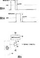
图3是使施加给各扫描线的扫描信号的振幅恒定的现有驱动方式的情况下,表示实际施加到显示板的某一列的显示像素上的电压VLCD的图。3 is a diagram showing a voltage VLCD actually applied to display pixels in a certain column of a display panel in a conventional driving method in which the amplitude of a scanning signal applied to each scanning line is constant.
在此,在图3中,为了说明简单,假设是在每1个场期间从输出端子输出的灰度信号的极性被反转的场反转驱动,用虚线示出的VL是从源极驱动器输出的灰度信号。此外,示出了从源极驱动器的各输出端子输出的灰度信号的大小恒定、即进行单一灰度的显示的情况。Here, in FIG. 3 , for the sake of simplicity of description, field inversion driving is assumed in which the polarity of the grayscale signal output from the output terminal is inverted every one field period. The grayscale signal output by the driver. In addition, the case where the magnitude of the gradation signal output from each output terminal of the source driver is constant, that is, a single gradation is performed, is shown.
在液晶显示装置中,已知在输入到TFT中的扫描信号的下降沿时,根据TFT的栅-源极间的寄生电容的电容Cgs、在像素电极与对置电极之间形成的液晶电容的电容CLCD、辅助电容的电容Cs和施加到TFT上的扫描信号的大小(振幅)Vg,施加到像素电极12上的信号电压(液晶施加电压VLCD)的大小,成为自从源极驱动器输出的灰度信号的电压值降下了馈通电压ΔV后的电压值。利用以下的式1表示该馈通电压ΔV。In a liquid crystal display device, it is known that at the falling edge of the scanning signal input to the TFT, the capacitance Cgs of the parasitic capacitance between the gate and the source of the TFT and the liquid crystal capacitance formed between the pixel electrode and the counter electrode are known to be The capacitance CLCD, the capacitance Cs of the auxiliary capacitor, the magnitude (amplitude) Vg of the scanning signal applied to the TFT, and the magnitude of the signal voltage (liquid crystal application voltage VLCD) applied to the
ΔV=(Cgs/Cs+CLCD+Cgs)×Vg (式1)ΔV=(Cgs/Cs+CLCD+Cgs)×Vg (Formula 1)
在此,如上所述地在显示板的一边侧安装了源极驱动器和栅极驱动器的结构中,如图1所示,从栅极驱动器向着形成在显示板的侧边上的栅极线端子布设着栅极布线组21b、21c、22b、22c。该情况下,各栅极布线的长度(布线长度)不同,大体上栅极布线组22c的布线长度比栅极布线组22b长,栅极布线组21c的布线长度比栅极布线组21b长。另外,包含在各栅极布线组21b~21c中的多个栅极布线的各个布线长度也不同。由于该布线长度的差异而使各栅极布线的布线电阻值产生差异,栅极布线组22c的布线电阻值比栅极布线组22b大,栅极布线组21c的布线电阻值比栅极布线组21b大。若该布线电阻值变大,由于布线电阻所引起的电压下降量的增加和布线电阻所引起的扫描信号的波形的上升/下降时间的增加,使得输入到显示像素中的扫描信号的振幅Vg实质上减少。若该扫描信号的振幅Vg减少,馈通电压ΔV的值就减少。这样,每行的馈通电压ΔV就变得不固定。Here, in the structure in which the source driver and the gate driver are mounted on one side of the display panel as described above, as shown in FIG.
图3示出的ΔVa、ΔVb、ΔVc、ΔVd表示显示板10的各区域A、B、C、D中的馈通电压ΔV。再有,在图3中,为了说明简单,以进行场反转驱动的情况为例子,但本实施方式的结构也可以同样地适用在线反转驱动中。ΔVa, ΔVb, ΔVc, and ΔVd shown in FIG. 3 represent feed-through voltages ΔV in the respective regions A, B, C, and D of the
如图3所示,若向驱动器输入垂直同步信号Vsync,就从栅极驱动器依次输出扫描信号,从显示板10的上侧行的显示像素开始依次成为选择状态。这样就从源极驱动器向已成为选择状态的显示像素输入灰度信号。该灰度信号与共通信号的电位差成为图3所示的电压VLCD。As shown in FIG. 3 , when a vertical synchronization signal Vsync is input to the driver, scanning signals are sequentially output from the gate driver, and the display pixels in the upper row of the
在此,在图1所示结构的显示装置中,由于栅极布线的布线长度有差异,因此各栅极布线的布线电阻不同,这样,输入到各栅极线中的扫描信号Vg的实质大小就不同,每行的馈通电压ΔV不同。因此,即使从源极驱动器输出的灰度信号的大小固定,如图3所示,实际施加到各显示像素的像素电极上的液晶施加电压VLCD,也成为自从源极驱动器输出的灰度信号的电压值下降了馈通电压ΔV后的电压值,因此,在1个场(或者1个帧)期间内不固定。Here, in the display device with the structure shown in FIG. 1, since the wiring length of the gate wiring is different, the wiring resistance of each gate wiring is different. In this way, the substantial magnitude of the scanning signal Vg input to each gate line Just different, the feedthrough voltage ΔV of each row is different. Therefore, even if the magnitude of the grayscale signal output from the source driver is fixed, as shown in FIG. Since the voltage value is lowered by the feed-through voltage ΔV, it is not fixed within one field (or one frame) period.
在此,在图3中,为了方便起见,假设在A、B、C、D的各区域内液晶施加电压VLCD是恒定的。由于实际上栅极布线长在各区域内都不同,因此在各区域内每个栅极线上ΔV也不同,各区域内的液晶施加电压VLCD严格来说也不恒定。但是,虽然取决于各区域的大小,但如果显示板10例如是使用在便携式电话机的显示部中的比较小的显示板,其1个区域的大小也较小,因此,1个区域内的液晶施加电压VLCD的差就小到人不能区别的程度,即使为了方便起见设为恒定,也不影响。Here, in FIG. 3 , it is assumed that the liquid crystal application voltage VLCD is constant in each of the regions A, B, C, and D for convenience. Since the gate wiring length actually differs in each region, ΔV varies for each gate line in each region, and the voltage VLCD applied to liquid crystal in each region is not strictly constant. However, although it depends on the size of each area, if the
对此,每个区域的液晶施加电压VLCD的差别较大,其结果,就存在不能保证显示的一致性,产生带状的显示斑纹、或者发生闪烁(画面的闪烁)等显示不佳的危险。On the other hand, the voltage VLCD applied to the liquid crystal varies greatly for each area, and as a result, display uniformity cannot be ensured, and there is a risk of poor display such as stripe-like display streaks or flickering (flickering of the screen).
于是,该第一实施方式通过控制扫描信号Vg的大小来使ΔV接近于恒定,由此实现显示品质的提高。Therefore, in the first embodiment, by controlling the magnitude of the scanning signal Vg, ΔV is kept close to constant, thereby improving the display quality.
图4是表示第一实施方式中的栅极驱动器的主要部分结构的电路图。FIG. 4 is a circuit diagram showing the configuration of main parts of the gate driver in the first embodiment.
图5A、5B是表示第一实施方式中的扫描信号的图。5A and 5B are diagrams showing scan signals in the first embodiment.
在此,图4所示的电路是例如对应栅极驱动器的各输出端子而设置的结构,示出了与其中的一个输出端子有关的部分。Here, the circuit shown in FIG. 4 is, for example, configured to correspond to each output terminal of the gate driver, and a portion related to one of the output terminals is shown.
该电路如图4所示,包括电阻负载31、选择开关32、栅极输出放大器33,例如与栅极驱动器中的移位寄存器34的各输出端子连接。As shown in FIG. 4 , the circuit includes a resistive load 31 , a selection switch 32 , and a
电阻负载31连接在电压VGH与接地之间,电阻分割电压VGH。选择开关32按照控制器的寄存器设定,选择电阻负载31中的期望大小的电压VGH’,作为偏压向栅极输出放大器33输出。这样,从栅极输出放大器33输出的扫描信号Vg的高电平侧的电压就成为电压VGH’。此外,低电平侧的电压是电压VGL。该电压VGH’是用于使显示像素的TFT11成为选择状态(导通状态)的电压,按每行设定适当的值。Resistive load 31 is connected between voltage VGH and ground, and divides voltage VGH by resistance. The selection switch 32 selects a voltage VGH' of a desired magnitude in the resistive load 31 according to the register setting of the controller, and outputs it to the
栅极输出放大器33按照来自控制器的垂直控制信号,将利用选择开关32设定的电压VGH’、或者用于使显示像素的TFT11成为非选择状态(关断状态)的电压信号VGL中的某一个作为扫描信号Vg,输出给对应的栅极线。The
利用如图4所示的结构,就能够如图5A和图5B所示地,按每个栅极线将扫描信号Vg的大小(振幅)设定为期望的值。这样就能够将每个栅极驱动器的馈通电压ΔV的值修正为期望值。With the structure shown in FIG. 4, as shown in FIGS. 5A and 5B, the magnitude (amplitude) of the scanning signal Vg can be set to a desired value for each gate line. This makes it possible to correct the value of the feed-through voltage ΔV of each gate driver to a desired value.
例如,在图5A中示出的第n线的扫描信号Vg是±15[V](VGH’与VGL的电位差(振幅)为30[V]),图5B中示出的第m线的扫描信号Vg是±14[V](VGH’与VGL的电位差(振幅)为28[V])的情况下,在它们之间可以使ΔV变化7%左右。通过将由使该扫描信号Vg的大小变化所产生的ΔV的变化量,设定为补偿每条栅极线上的因栅极驱动器与显示板10之间的栅极布线的布线电阻所引起的馈通电压ΔV之差的值,就能够使各栅极线中的馈通电压ΔV的值接近于均等。For example, the scanning signal Vg of the nth line shown in FIG. 5A is ±15 [V] (the potential difference (amplitude) between VGH' and VGL is 30 [V]), and the scanning signal Vg of the mth line shown in FIG. 5B When the scanning signal Vg is ±14 [V] (the potential difference (amplitude) between VGH′ and VGL is 28 [V]), ΔV can be changed by about 7% between them. By setting the amount of change in ΔV caused by changing the magnitude of the scanning signal Vg to compensate for the feedback caused by the wiring resistance of the gate wiring between the gate driver and the
例如,关于如图3所示的现有驱动方式中馈通电压ΔV相对于作为某一基准的馈通电压ΔV(要得到作为期望的液晶施加电压VLCD的馈通电压ΔV)比较小的、例如栅极布线的布线电阻比较大的显示板10的区域A、C的各行,使在选择开关32中选择的电压高于对基准的馈通电压ΔV选择的基准的电压,使扫描信号Vg的大小(振幅)大于对基准的馈通电压ΔV设定的电压值。For example, in the conventional driving method shown in FIG. 3 , the feed-through voltage ΔV is relatively small relative to the feed-through voltage ΔV as a certain reference (to obtain the feed-through voltage ΔV as the desired liquid crystal application voltage VLCD), for example In each row of the regions A and C of the
此外,关于在现有驱动方式中馈通电压ΔV对基准的馈通电压ΔV比较大的、例如栅极布线的布线电阻比较小的显示板10的区域B、D的各行,使在选择开关32中选择的电压低于对基准的馈通电压ΔV选择的基准的电压,使扫描信号Vg的大小(振幅)小于对基准的馈通电压ΔV设定的电压值。通过这样做,就能够使显示板10的每行的馈通电压ΔV的大小接近于均等。这样就能够在整个显示板10上得到均匀的显示。In addition, for each row of the
如以上说明,根据第一实施方式,通过对每行修正从栅极驱动器输出的扫描信号的大小(振幅),就能够使各栅极线中的ΔV接近于恒定。这样就能实现显示品质的提高。As described above, according to the first embodiment, by correcting the magnitude (amplitude) of the scanning signal output from the gate driver for each row, ΔV in each gate line can be made nearly constant. This enables improvement in display quality.
再有,在上述记载中,对显示板的各行设置了设定扫描信号Vg的大小的图4中示出的电路,但例如也可以将显示板10的各区域A、B、C、D中的扫描信号Vg的大小设为一定,对驱动器21、22的左右的每个栅极驱动器各设置设定扫描信号Vg的大小的电路。In addition, in the above description, the circuit shown in FIG. 4 for setting the magnitude of the scanning signal Vg is provided for each row of the display panel, but for example, it is also possible to set the circuit in each area A, B, C, and D of the
此外,在图1中示出的结构中,由于栅极布线的布线电阻(特别是布线长度)的不同而使ΔV产生差异,但如式1所示,由于馈通电压ΔV也根据TFT11的栅-源极间的寄生电容的电容量、液晶电容的电容量和辅助电容的电容量进行变化,因此,在它们中有偏差的情况下,每行中也产生馈通电压ΔV之差。在该情况下,通过测量例如每行的馈通电压ΔV,与之相应地改变每行的Vg的大小,就能使各栅极线中的馈通电压ΔV接近于固定值。In addition, in the structure shown in FIG. 1, ΔV is different due to the difference in the wiring resistance (especially the wiring length) of the gate wiring, but as shown in Formula 1, since the feedthrough voltage ΔV also depends on the gate - The capacitance of the parasitic capacitance between the sources, the capacitance of the liquid crystal capacitor, and the capacitance of the auxiliary capacitor varies, and therefore, when there is a deviation among them, a difference in the feed-through voltage ΔV also occurs in each row. In this case, for example, by measuring the feedthrough voltage ΔV for each row and changing the magnitude of Vg for each row accordingly, the feedthrough voltage ΔV in each gate line can be brought close to a fixed value.
图6是表示第一实施方式的变形例中的栅极驱动器的主要部分结构的电路图。图7是表示第一实施方式的变形例中的扫描信号的图。FIG. 6 is a circuit diagram showing a configuration of main parts of a gate driver in a modified example of the first embodiment. FIG. 7 is a diagram showing scanning signals in a modified example of the first embodiment.
在上述的第一实施方式中,通过使设定扫描信号Vg的高电平侧的电压的栅极输出放大器33的偏压值适当变化,来改变扫描信号Vg的振幅,从而使馈通电压ΔV变化。In the first embodiment described above, the amplitude of the scanning signal Vg is changed by appropriately changing the bias voltage value of the
对此,如图6所示,例如也可以具有使供给栅极输出放大器33的偏置电流的值可变的偏置电流设定电路35,将施加给栅极输出放大器33的偏压恒定,来适当改变供给栅极输出放大器33的偏置电流的值,从而使栅极输出放大器33的驱动能力可变。In contrast, as shown in FIG. 6 , for example, a bias
该情况下,例如通过减少供给栅极输出放大器33的偏置电流的值而使栅极输出放大器33的驱动能力比较低,就如图7所示,能够增加通过栅极布线施加到栅极线上的扫描信号的波形的圆滑,增加扫描信号的上升/下降时间,降低实质上施加给显示像素的扫描信号的振幅Vg,这样就能够减少馈通电压ΔV的大小。In this case, for example, by reducing the value of the bias current supplied to the
也可以通过这样地改变栅极输出放大器33的驱动能力,来改变实质上施加给显示像素的扫描信号的振幅Vg,从而使馈通电压ΔV的大小变化。It is also possible to change the amplitude Vg of the scanning signal substantially applied to the display pixel by changing the driving capability of the
[第二实施方式][Second Embodiment]
下面,说明本发明的第二实施方式。本发明的第二实施方式是考虑每行的ΔV的差异,通过修正从源极驱动器输出的灰度信号自身,来控制施加给显示像素的电压VLCD的方法。Next, a second embodiment of the present invention will be described. The second embodiment of the present invention is a method of controlling the voltage VLCD applied to the display pixels by correcting the grayscale signal itself output from the source driver in consideration of the difference in ΔV for each row.
图8是说明第二实施方式的方法的概念的图。FIG. 8 is a diagram illustrating the concept of the method of the second embodiment.
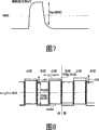
在此,图8中示出的Vsig(input)是表示从源极驱动器的一个输出端子输出的灰度信号的每行变化的波形,Vsig(VLCD)是实际上供给像素电极12的液晶施加电压的波形,Vcom是向对置电极13输入的共通信号的波形。Here, Vsig(input) shown in FIG. 8 is a waveform representing a change in each line of a grayscale signal output from one output terminal of the source driver, and Vsig(VLCD) is a liquid crystal application voltage actually supplied to the
在此,图8示出了图1中的区域A和区域B的边界附近的行。此外,在图8中,为了说明简单,示出了进行单一灰度的显示的情况。Here, FIG. 8 shows rows near the boundary of area A and area B in FIG. 1 . In addition, in FIG. 8, for the sake of simplicity of description, a case where a single gray scale is displayed is shown.
此外,图8示出了使灰度信号Vsig(input)和共通信号Vcom的极性每1行反转一次的线反转驱动的例子,但第二实施方式的方法在如图3所示的场反转驱动中也能适用。此外,图8示出区域A和区域B的驱动的情况,但区域C和区域D的驱动也按照区域A和区域B的驱动进行。8 shows an example of line inversion driving in which the polarities of the gradation signal Vsig (input) and the common signal Vcom are reversed every row. It is also applicable to field inversion driving. In addition, although FIG. 8 shows the driving of the region A and the region B, the driving of the region C and the region D is also performed in the same manner as the driving of the region A and the region B.
在图8中,最初的3条线的期间与区域A相对应,它以后的与区域B相对应。在此,若设区域A中的馈通电压ΔV为ΔV1,区域B中的馈通电压ΔV为ΔV2,则为了向像素电极12供给大小一定的Vsig(VLCD),就最好要在区域A的期间供给比Vsig(VLCD)高ΔV1的灰度信号Vsig(input),在区域B的期间供给比Vsig(VLCD)高ΔV2的灰度信号Vsig(input)。这样,就始终向各显示像素施加Vsig(VLCD)与共通信号Vcom的电位差、即具有固定大小的电压VLCD,能够提高显示品质。In FIG. 8 , the period of the first three lines corresponds to area A, and the period thereafter corresponds to area B. Here, if the feed-through voltage ΔV in the region A is ΔV1, and the feed-through voltage ΔV in the region B is ΔV2, then in order to supply a constant Vsig (VLCD) to the
图9是表示第二实施方式中的源极驱动器的主要部分结构的电路图。FIG. 9 is a circuit diagram showing a configuration of a main part of a source driver in a second embodiment.
在此,图9中示出的电路是对应源极驱动器的各输出端子设置的。该电路如图9所示,包括γ电阻负载41、电阻负载42a、42b、灰度选择部43、源极输出放大器44,灰度选择部43例如与未图示的数据锁存电路的输出端子连接。Here, the circuit shown in FIG. 9 is provided corresponding to each output terminal of the source driver. As shown in FIG. 9, the circuit includes a
γ电阻负载41通过电阻分割生成与显示数据可取的所有灰度电平相对应的多个灰度信号,灰度选择部43选择与显示数据的灰度值相对应的灰度信号后,施加给源极输出放大器44。此外,通过电阻负载42a、42b向γ电阻负载41施加高电位电压VGMH和低电位电压VGML。在此,在进行线反转驱动的情况下,例如由灰度选择部43选择的灰度信号按照从控制器输出的极性控制信号,每1行反转一次,灰度信号对于共通信号Vcom的极性每1行反转一次。The gamma
即,在图8中示出的例如第1行的正极性期间,根据显示数据的灰度值,由灰度选择部43选择成为比共通信号Vcom高电位的这样的灰度信号。反之,在例如第2行的负极性期间,根据显示数据的灰度值,由灰度选择部43选择成为比共通信号Vcom低电位的这样的灰度信号。That is, in the positive polarity period of, for example, the first row shown in FIG. 8 , the gradation signal having a higher potential than the common signal Vcom is selected by the
按照控制器的寄存器设定,将电阻负载42a、电阻负载42b变更设定为电阻值与每行的馈通电压ΔV的大小相对应的值,使施加给γ电阻负载41的电压范围偏移与每行的馈通电压ΔV的大小相对应的规定量。即,关于具有相对于成为某一基准的馈通电压ΔV比较大的馈通电压ΔV的行,通过使电阻负载42a的电阻值小于对基准的馈通电压ΔV设定的基准的电阻值,使电阻负载42b的电阻值大于对基准的馈通电压ΔV设定的基准的电阻值,就使施加给γ电阻负载41的电压范围相对于对基准的馈通电压ΔV设定的电压范围向高电压侧偏移规定量。此外,关于具有相对于基准的馈通电压ΔV较小的馈通电压ΔV的行,通过在正极性期间使与电压VGMH连接的电阻负载42a的电阻值大于基准的电阻值,使得与电压VGML连接的电阻负载42b的电阻值小于基准的电阻值,就使施加给γ电阻负载41的电压范围相对于对基准的馈通电压ΔV设定的电压范围向低电压侧偏移规定量。这样,就使灰度信号相对于对基准的馈通电压ΔV设定的值,向高电压侧或低电压侧偏移与馈通电压ΔV的大小相对应的电压。这样,就能够得到如图8所示的波形的Vsig(input),在进行单一灰度的显示的情况下,即使馈通电压ΔV的大小不同,也能够向像素电极12供给一定的电压Vsig(VLCD)。According to the register settings of the controller, the
灰度选择部43从在γ电阻负载41中生成的多个灰度信号中,选择与显示数据的灰度电平相对应的灰度信号后,向源极输出放大器44输出。源极输出放大器44按照它的驱动能力,放大来自灰度选择部43的灰度信号后,向对应的显示像素的像素电极12输出。The
再有,在上述记载中,根据馈通电压ΔV的大小,对每行各设定电阻负载42a、42b的电阻值,但例如也可以对显示板10的各区域A、B、C、D设定电阻负载42a、42b的电阻值。Furthermore, in the above description, the resistance values of the
此外,在上述记载中,在进行线反转驱动的情况下,构成为将灰度选择部43选择的灰度信号按每1行反转一次,但也可以构成为将通过电阻负载42a、42b施加到γ电阻负载41上的电位VGMH、VGML按每1行反转一次,使由灰度选择部43选择的灰度信号不反转。In addition, in the above description, when line inversion driving is performed, the gradation signal selected by the
如以上说明,根据第二实施方式,通过按照各行的馈通电压ΔV的大小修正从源极驱动器输出的灰度信号的大小,就能控制因馈通电压ΔV之差所引起的显示品质的降低,实现显示品质的提高。As described above, according to the second embodiment, by correcting the magnitude of the gradation signal output from the source driver according to the magnitude of the feedthrough voltage ΔV of each row, it is possible to suppress the deterioration of the display quality due to the difference in the feedthrough voltage ΔV. , to improve the display quality.
[第三实施方式][Third Embodiment]
下面,说明本发明的第三实施方式。在上述的第二实施方式中,考虑每行的馈通电压ΔV之差,修正从源极驱动器输出的灰度信号的大小,但由于施加给显示像素的电压VLCD是灰度信号与共通信号的电位差,因此,通过修正共通信号的大小,也能够与第二实施方式同样地控制施加给显示像素的电压VLCD。Next, a third embodiment of the present invention will be described. In the above-mentioned second embodiment, the difference between the feed-through voltage ΔV of each row is considered, and the magnitude of the grayscale signal output from the source driver is corrected, but since the voltage VLCD applied to the display pixel is the difference between the grayscale signal and the common signal Therefore, by correcting the magnitude of the common signal, it is also possible to control the voltage VLCD applied to the display pixels in the same manner as in the second embodiment.
图10是表示第三实施方式中的共通信号输出电路的主要部分结构的电路图。FIG. 10 is a circuit diagram showing a configuration of main parts of a common signal output circuit in a third embodiment.
在此,图10中示出的共通信号输出电路包括数模转换器(DAC)51a、51b、共通信号输出放大器52a、52b和极性切换开关53。Here, the common signal output circuit shown in FIG. 10 includes digital-to-analog converters (DACs) 51 a , 51 b , common
DAC51a具有按照控制器的寄存器设定的大小,在正极性期间生成比灰度信号低电位的共通信号。共通信号输出放大器52a按照其驱动能力放大来自DAC51a的共通信号后,向极性切换开关53输出。The DAC 51 a has a magnitude set in a register of the controller, and generates a common signal having a lower potential than the grayscale signal during the positive polarity period. The common
DAC51b具有按照控制器的寄存器设定的大小,在负极性期间生成比灰度信号高电位的共通信号。共通信号输出放大器52b按照其驱动能力放大来自DBC51b的共通信号后,向极性切换开关53输出。The
在此,按照每行的馈通电压ΔV的大小,设定对DAC51a和DAC51b设定的共通信号的大小。Here, the magnitude of the common signal set for DAC51a and DAC51b is set according to the magnitude of feed-through voltage ΔV for each row.
即,在正极性期间,关于具有相对于成为某一基准的馈通电压ΔV较大的馈通电压ΔV的行,使对DAC51a设定的共通信号的大小比对基准的馈通电压ΔV设定的基准的共通信号的大小较小,关于具有相对于基准的馈通电压ΔV较小的馈通电压ΔV的行,使对DAC51a设定的共通信号的大小比基准的共通信号的大小较大。That is, in the positive polarity period, for a row having a larger feed-through voltage ΔV than a certain reference feed-through voltage ΔV, the magnitude of the common signal set to the DAC 51a is set with respect to the reference feed-through voltage ΔV. The magnitude of the reference common signal is small, and the magnitude of the common signal set to the DAC 51a is larger than the magnitude of the reference common signal for a row having a smaller feed-through voltage ΔV than the reference feed-through voltage ΔV.
此外,在负极性期间,关于具有相对于基准的馈通电压ΔV较大的馈通电压ΔV的行,使对DAC51b设定的共通信号的大小比对基准的馈通电压ΔV设定的基准的共通信号的大小较小,关于具有相对于基准的馈通电压ΔV较小的馈通电压ΔV的行,使对DAC51b设定的共通信号的大小比基准的共通信号的大小较大。这样,就如图8的Vsig(VLCD)所示,在进行单一灰度的显示的情况下,即使馈通电压ΔV的大小不同,也能够向像素电极12供给固定的电压Vsig(VLCD)。In addition, during the negative polarity period, the magnitude of the common signal set to the
极性切换开关53按照来自未图示的控制器的极性控制信号,切换向显示像素输出的共通信号的极性。The
再有,在上述记载中,按照馈通电压ΔV的大小,对每行设定共通信号的大小,但例如也可以对显示板10的每个区域A、B、C、D设定共通信号的大小。In addition, in the above description, the magnitude of the common signal is set for each row according to the magnitude of the feed-through voltage ΔV, but for example, the magnitude of the common signal may be set for each of the regions A, B, C, and D of the
如以上说明,根据第三实施方式,通过考虑馈通电压ΔV之差,对每行修正从共通信号发生电路输出的共通信号的大小,就能实现显示品质的提高。As described above, according to the third embodiment, the display quality can be improved by correcting the magnitude of the common signal output from the common signal generating circuit for each row in consideration of the difference in the feedthrough voltage ΔV.
以上基于实施方式说明了本发明,但本发明不限定于上述的实施方式,当然可以在本发明的主旨范围内进行各种各样的变形和应用。As mentioned above, although this invention was demonstrated based on embodiment, this invention is not limited to said embodiment, It goes without saying that various deformation|transformation and application are possible within the scope of this invention.
另外,在上述的实施方式中包含着各种各样阶段的发明,利用公开的多个结构要件的适当组合能抽出各种各样的发明。例如,即使从实施方式中示出的全部结构要件删掉几个结构要件,也能够解决如上所述的课题,在得到上述这样的效果的情况下,也能抽出删掉了该结构要件的结构作为发明。In addition, inventions of various stages are included in the above-mentioned embodiments, and various inventions can be extracted by appropriate combinations of a plurality of disclosed constituent elements. For example, even if a few structural requirements are deleted from all the structural requirements shown in the embodiment, the above-mentioned problems can be solved, and when the above-mentioned effects are obtained, the structure from which the structural requirements have been deleted can also be extracted. as an invention.
本领域的技术人员会很容易地得到其它优点和变形。因此,本发明在其更多方面并不局限于本文中所示出并描述的特定细节和有代表性的实施例。因而,在不脱离由所附的权利要求和其等效内容所限定的本发明原理的精神或范围的情况下可以作出各种变形。Additional advantages and modifications will readily appear to those skilled in the art. Therefore, the invention in its further aspects is not limited to the specific details and representative embodiments shown and described herein. Accordingly, various modifications may be made without departing from the spirit or scope of the principles of the invention as defined by the appended claims and their equivalents.
Claims (5)
Translated fromChineseApplications Claiming Priority (2)
| Application Number | Priority Date | Filing Date | Title |
|---|---|---|---|
| JP2006259424AJP4400605B2 (en) | 2006-09-25 | 2006-09-25 | Display driving device and display device |
| JP259424/2006 | 2006-09-25 |
Publications (2)
| Publication Number | Publication Date |
|---|---|
| CN101154367A CN101154367A (en) | 2008-04-02 |
| CN101154367Btrue CN101154367B (en) | 2012-05-23 |
Family
ID=39224426
Family Applications (1)
| Application Number | Title | Priority Date | Filing Date |
|---|---|---|---|
| CN2007101537979AExpired - Fee RelatedCN101154367B (en) | 2006-09-25 | 2007-09-25 | Display driving apparatus and display apparatus comprising the same |
Country Status (5)
| Country | Link |
|---|---|
| US (1) | US8159447B2 (en) |
| JP (1) | JP4400605B2 (en) |
| KR (1) | KR100901061B1 (en) |
| CN (1) | CN101154367B (en) |
| TW (1) | TWI387955B (en) |
Families Citing this family (31)
| Publication number | Priority date | Publication date | Assignee | Title |
|---|---|---|---|---|
| TWI406235B (en)* | 2008-05-08 | 2013-08-21 | Chunghwa Picture Tubes Ltd | Liquid crystal display and switching voltage controlling circuit thereof |
| CN101635133B (en)* | 2008-07-21 | 2013-10-16 | 群创光电股份有限公司 | Liquid crystal display device and pixel driving method |
| TWI398849B (en)* | 2008-12-10 | 2013-06-11 | Au Optronics Corp | Method for driving display panel |
| WO2010073775A1 (en)* | 2008-12-25 | 2010-07-01 | シャープ株式会社 | Display device and display device drive method |
| TWI380109B (en)* | 2009-01-23 | 2012-12-21 | Au Optronics Corp | Display device and method of equalizing loading effect of display device |
| CN102334153B (en)* | 2009-03-18 | 2013-12-04 | 夏普株式会社 | display device |
| JP5029670B2 (en) | 2009-09-28 | 2012-09-19 | カシオ計算機株式会社 | Display device |
| TWI399606B (en)* | 2009-10-05 | 2013-06-21 | Au Optronics Corp | Active device array substrate and display panel thereof |
| JP5018920B2 (en) | 2010-03-24 | 2012-09-05 | 株式会社デンソー | A / D converter |
| TWI421573B (en)* | 2010-11-08 | 2014-01-01 | Au Optronics Corp | Gate driver and method of layout of gate driver |
| CN102568406A (en)* | 2010-12-31 | 2012-07-11 | 北京京东方光电科技有限公司 | Grid line driving method and device of liquid crystal display |
| TWI530926B (en)* | 2011-05-03 | 2016-04-21 | 天鈺科技股份有限公司 | Source driver and display apparatus |
| CN102708815B (en)* | 2011-12-14 | 2014-08-06 | 京东方科技集团股份有限公司 | Gate driving circuit and liquid crystal display device |
| KR101920761B1 (en) | 2011-12-26 | 2018-11-22 | 엘지디스플레이 주식회사 | Array substrate for flat display device and flat display device comprising the same |
| WO2013099189A1 (en)* | 2011-12-28 | 2013-07-04 | シャープ株式会社 | Display apparatus |
| KR101952936B1 (en)* | 2012-05-23 | 2019-02-28 | 삼성디스플레이 주식회사 | Display device and driving method thereof |
| CN103295540B (en)* | 2012-06-07 | 2015-06-10 | 上海天马微电子有限公司 | Driving method and driving device of active matrix display panel and display |
| KR101549291B1 (en)* | 2012-10-25 | 2015-09-02 | 엘지디스플레이 주식회사 | Display device |
| KR102008133B1 (en)* | 2012-12-12 | 2019-08-08 | 엘지디스플레이 주식회사 | Display device and driving method thereof |
| JP2015045726A (en)* | 2013-08-28 | 2015-03-12 | シナプティクス・ディスプレイ・デバイス株式会社 | Display drive device and display device |
| GB2519084A (en)* | 2013-10-08 | 2015-04-15 | Plastic Logic Ltd | Transistor addressing |
| JP2015090414A (en)* | 2013-11-06 | 2015-05-11 | シナプティクス・ディスプレイ・デバイス株式会社 | Display drive circuit and display device |
| KR20160005859A (en) | 2014-07-07 | 2016-01-18 | 삼성디스플레이 주식회사 | Display device |
| KR102244693B1 (en)* | 2014-11-10 | 2021-04-27 | 삼성디스플레이 주식회사 | Display apparatus |
| CN107610645B (en)* | 2017-10-26 | 2020-04-28 | 上海天马有机发光显示技术有限公司 | An OLED display panel, its driving method and display device |
| CN109166502B (en)* | 2018-09-12 | 2020-10-16 | 惠科股份有限公司 | Detection method and display panel |
| CN111261081B (en)* | 2018-11-30 | 2021-10-19 | 北京小米移动软件有限公司 | Screen display method and device |
| CN109346023A (en)* | 2018-12-13 | 2019-02-15 | 惠科股份有限公司 | Driving device and driving method of display device |
| CN109584833B (en)* | 2019-01-21 | 2021-06-01 | 深圳市华星光电半导体显示技术有限公司 | Display panel and display device |
| CN114927112B (en)* | 2022-05-19 | 2024-06-25 | 滁州惠科光电科技有限公司 | Control method and control circuit of display panel and display device |
| TWI850720B (en)* | 2022-07-27 | 2024-08-01 | 友達光電股份有限公司 | Driving device |
Citations (2)
| Publication number | Priority date | Publication date | Assignee | Title |
|---|---|---|---|---|
| CN1532795A (en)* | 2003-03-25 | 2004-09-29 | ��������ʾ���Ƽ���˾ | Liquid crystal driving device and driving method thereof |
| CN2757167Y (en)* | 2004-07-22 | 2006-02-08 | 比亚迪股份有限公司 | Liquid display screen |
Family Cites Families (13)
| Publication number | Priority date | Publication date | Assignee | Title |
|---|---|---|---|---|
| JPH04293014A (en) | 1991-03-22 | 1992-10-16 | Fujitsu Ltd | Matrix type crystal display device |
| JPH10186325A (en) | 1996-12-27 | 1998-07-14 | Fujitsu Ltd | LCD panel |
| KR100271092B1 (en) | 1997-07-23 | 2000-11-01 | 윤종용 | A liquid crystal display having different common voltage |
| JP2002123228A (en)* | 2000-10-17 | 2002-04-26 | Seiko Epson Corp | Electro-optical panel, driving method thereof, and electronic device |
| JP2002182614A (en) | 2000-12-11 | 2002-06-26 | Seiko Epson Corp | Semiconductor device |
| KR100559223B1 (en)* | 2000-12-29 | 2006-03-15 | 비오이 하이디스 테크놀로지 주식회사 | LC Module |
| TWI267050B (en)* | 2001-11-26 | 2006-11-21 | Samsung Electronics Co Ltd | Liquid crystal display and driving method thereof |
| KR100864489B1 (en) | 2002-05-14 | 2008-10-20 | 삼성전자주식회사 | Liquid crystal display |
| JP2004086093A (en)* | 2002-08-29 | 2004-03-18 | Sharp Corp | Liquid crystal drive |
| US7142116B2 (en) | 2003-03-19 | 2006-11-28 | Honda Motor Co., Ltd. | Article management system |
| KR100831306B1 (en)* | 2004-03-17 | 2008-05-22 | 엘지디스플레이 주식회사 | LCD display device |
| JP2006106142A (en)* | 2004-09-30 | 2006-04-20 | Toshiba Corp | Display device and display method |
| JP2006133511A (en) | 2004-11-05 | 2006-05-25 | Sharp Corp | Active matrix display device |
- 2006
- 2006-09-25JPJP2006259424Apatent/JP4400605B2/ennot_activeExpired - Fee Related
- 2007
- 2007-09-06USUS11/899,581patent/US8159447B2/ennot_activeExpired - Fee Related
- 2007-09-21KRKR1020070096644Apatent/KR100901061B1/ennot_activeExpired - Fee Related
- 2007-09-21TWTW096135347Apatent/TWI387955B/ennot_activeIP Right Cessation
- 2007-09-25CNCN2007101537979Apatent/CN101154367B/ennot_activeExpired - Fee Related
Patent Citations (2)
| Publication number | Priority date | Publication date | Assignee | Title |
|---|---|---|---|---|
| CN1532795A (en)* | 2003-03-25 | 2004-09-29 | ��������ʾ���Ƽ���˾ | Liquid crystal driving device and driving method thereof |
| CN2757167Y (en)* | 2004-07-22 | 2006-02-08 | 比亚迪股份有限公司 | Liquid display screen |
Also Published As
| Publication number | Publication date |
|---|---|
| KR20080027746A (en) | 2008-03-28 |
| US20080074404A1 (en) | 2008-03-27 |
| CN101154367A (en) | 2008-04-02 |
| TW200822054A (en) | 2008-05-16 |
| US8159447B2 (en) | 2012-04-17 |
| KR100901061B1 (en) | 2009-06-04 |
| JP2008077005A (en) | 2008-04-03 |
| JP4400605B2 (en) | 2010-01-20 |
| TWI387955B (en) | 2013-03-01 |
Similar Documents
| Publication | Publication Date | Title |
|---|---|---|
| CN101154367B (en) | Display driving apparatus and display apparatus comprising the same | |
| JP4199141B2 (en) | Display signal processing device and display device | |
| US7777713B2 (en) | Device and method for driving large-sized and high-resolution display panel | |
| JP4284494B2 (en) | Display device and drive control method thereof | |
| US20050253829A1 (en) | Display device and display device driving method | |
| WO2010073775A1 (en) | Display device and display device drive method | |
| WO2010087051A1 (en) | Display device and display device driving method | |
| US20120120044A1 (en) | Liquid crystal display device and method for driving the same | |
| US10832627B2 (en) | Display apparatus and source driver thereof and operating method | |
| US11501729B2 (en) | Source driver that adjusts a timing of outputting of pixel data based on a length of a source line, and display device | |
| KR100840331B1 (en) | Common voltage generator and liquid crystal display using same | |
| CN102013237A (en) | Driving device for driving a liquid crystal display panel and related display device | |
| KR20070116408A (en) | Liquid crystal display device and driving method thereof | |
| WO2009133906A1 (en) | Video signal line drive circuit and liquid crystal display device | |
| KR20100063170A (en) | Liquid crystal display device | |
| CN101939779B (en) | Driving circuit of liquid crystal display device | |
| JP5024311B2 (en) | Driving method of display device | |
| US20060087485A1 (en) | Electro-optic device | |
| JP5418388B2 (en) | Liquid crystal display | |
| US20110043506A1 (en) | Device for Driving LCD panel and Related Display Device | |
| KR101127850B1 (en) | Driving circuit of liquid crystal display device | |
| US9928800B2 (en) | Display apparatus and a method of driving the same | |
| KR101107676B1 (en) | Pixel Charge Compensation Circuit and Method of Liquid Crystal Display | |
| KR101123332B1 (en) | device and method for gamma voltage supply | |
| JP2007232965A (en) | Display driving device and display device including the same |
Legal Events
| Date | Code | Title | Description |
|---|---|---|---|
| C06 | Publication | ||
| PB01 | Publication | ||
| C10 | Entry into substantive examination | ||
| SE01 | Entry into force of request for substantive examination | ||
| C14 | Grant of patent or utility model | ||
| GR01 | Patent grant | ||
| CF01 | Termination of patent right due to non-payment of annual fee | ||
| CF01 | Termination of patent right due to non-payment of annual fee | Granted publication date:20120523 Termination date:20160925 |