CN101154343A - display screen - Google Patents
display screenDownload PDFInfo
- Publication number
- CN101154343A CN101154343ACNA200710162011XACN200710162011ACN101154343ACN 101154343 ACN101154343 ACN 101154343ACN A200710162011X ACNA200710162011X ACN A200710162011XACN 200710162011 ACN200710162011 ACN 200710162011ACN 101154343 ACN101154343 ACN 101154343A
- Authority
- CN
- China
- Prior art keywords
- transistor
- wiring
- gate
- electrode
- signal
- Prior art date
- Legal status (The legal status is an assumption and is not a legal conclusion. Google has not performed a legal analysis and makes no representation as to the accuracy of the status listed.)
- Granted
Links
Images


Classifications
- H—ELECTRICITY
- H10—SEMICONDUCTOR DEVICES; ELECTRIC SOLID-STATE DEVICES NOT OTHERWISE PROVIDED FOR
- H10D—INORGANIC ELECTRIC SEMICONDUCTOR DEVICES
- H10D86/00—Integrated devices formed in or on insulating or conducting substrates, e.g. formed in silicon-on-insulator [SOI] substrates or on stainless steel or glass substrates
- H10D86/40—Integrated devices formed in or on insulating or conducting substrates, e.g. formed in silicon-on-insulator [SOI] substrates or on stainless steel or glass substrates characterised by multiple TFTs
- H10D86/60—Integrated devices formed in or on insulating or conducting substrates, e.g. formed in silicon-on-insulator [SOI] substrates or on stainless steel or glass substrates characterised by multiple TFTs wherein the TFTs are in active matrices
- G—PHYSICS
- G09—EDUCATION; CRYPTOGRAPHY; DISPLAY; ADVERTISING; SEALS
- G09G—ARRANGEMENTS OR CIRCUITS FOR CONTROL OF INDICATING DEVICES USING STATIC MEANS TO PRESENT VARIABLE INFORMATION
- G09G3/00—Control arrangements or circuits, of interest only in connection with visual indicators other than cathode-ray tubes
- G09G3/20—Control arrangements or circuits, of interest only in connection with visual indicators other than cathode-ray tubes for presentation of an assembly of a number of characters, e.g. a page, by composing the assembly by combination of individual elements arranged in a matrix no fixed position being assigned to or needed to be assigned to the individual characters or partial characters
- G09G3/34—Control arrangements or circuits, of interest only in connection with visual indicators other than cathode-ray tubes for presentation of an assembly of a number of characters, e.g. a page, by composing the assembly by combination of individual elements arranged in a matrix no fixed position being assigned to or needed to be assigned to the individual characters or partial characters by control of light from an independent source
- G09G3/36—Control arrangements or circuits, of interest only in connection with visual indicators other than cathode-ray tubes for presentation of an assembly of a number of characters, e.g. a page, by composing the assembly by combination of individual elements arranged in a matrix no fixed position being assigned to or needed to be assigned to the individual characters or partial characters by control of light from an independent source using liquid crystals
- G09G3/3611—Control of matrices with row and column drivers
- G09G3/3674—Details of drivers for scan electrodes
- G09G3/3677—Details of drivers for scan electrodes suitable for active matrices only
- G—PHYSICS
- G09—EDUCATION; CRYPTOGRAPHY; DISPLAY; ADVERTISING; SEALS
- G09G—ARRANGEMENTS OR CIRCUITS FOR CONTROL OF INDICATING DEVICES USING STATIC MEANS TO PRESENT VARIABLE INFORMATION
- G09G3/00—Control arrangements or circuits, of interest only in connection with visual indicators other than cathode-ray tubes
- G09G3/20—Control arrangements or circuits, of interest only in connection with visual indicators other than cathode-ray tubes for presentation of an assembly of a number of characters, e.g. a page, by composing the assembly by combination of individual elements arranged in a matrix no fixed position being assigned to or needed to be assigned to the individual characters or partial characters
- G09G3/2092—Details of a display terminals using a flat panel, the details relating to the control arrangement of the display terminal and to the interfaces thereto
- G—PHYSICS
- G11—INFORMATION STORAGE
- G11C—STATIC STORES
- G11C19/00—Digital stores in which the information is moved stepwise, e.g. shift registers
- G11C19/28—Digital stores in which the information is moved stepwise, e.g. shift registers using semiconductor elements
- H—ELECTRICITY
- H10—SEMICONDUCTOR DEVICES; ELECTRIC SOLID-STATE DEVICES NOT OTHERWISE PROVIDED FOR
- H10D—INORGANIC ELECTRIC SEMICONDUCTOR DEVICES
- H10D86/00—Integrated devices formed in or on insulating or conducting substrates, e.g. formed in silicon-on-insulator [SOI] substrates or on stainless steel or glass substrates
- H10D86/40—Integrated devices formed in or on insulating or conducting substrates, e.g. formed in silicon-on-insulator [SOI] substrates or on stainless steel or glass substrates characterised by multiple TFTs
- H10D86/421—Integrated devices formed in or on insulating or conducting substrates, e.g. formed in silicon-on-insulator [SOI] substrates or on stainless steel or glass substrates characterised by multiple TFTs having a particular composition, shape or crystalline structure of the active layer
- H10D86/423—Integrated devices formed in or on insulating or conducting substrates, e.g. formed in silicon-on-insulator [SOI] substrates or on stainless steel or glass substrates characterised by multiple TFTs having a particular composition, shape or crystalline structure of the active layer comprising semiconductor materials not belonging to the Group IV, e.g. InGaZnO
- H—ELECTRICITY
- H10—SEMICONDUCTOR DEVICES; ELECTRIC SOLID-STATE DEVICES NOT OTHERWISE PROVIDED FOR
- H10D—INORGANIC ELECTRIC SEMICONDUCTOR DEVICES
- H10D86/00—Integrated devices formed in or on insulating or conducting substrates, e.g. formed in silicon-on-insulator [SOI] substrates or on stainless steel or glass substrates
- H10D86/40—Integrated devices formed in or on insulating or conducting substrates, e.g. formed in silicon-on-insulator [SOI] substrates or on stainless steel or glass substrates characterised by multiple TFTs
- H10D86/441—Interconnections, e.g. scanning lines
- H—ELECTRICITY
- H10—SEMICONDUCTOR DEVICES; ELECTRIC SOLID-STATE DEVICES NOT OTHERWISE PROVIDED FOR
- H10D—INORGANIC ELECTRIC SEMICONDUCTOR DEVICES
- H10D89/00—Aspects of integrated devices not covered by groups H10D84/00 - H10D88/00
- H10D89/10—Integrated device layouts
- G—PHYSICS
- G09—EDUCATION; CRYPTOGRAPHY; DISPLAY; ADVERTISING; SEALS
- G09G—ARRANGEMENTS OR CIRCUITS FOR CONTROL OF INDICATING DEVICES USING STATIC MEANS TO PRESENT VARIABLE INFORMATION
- G09G2300/00—Aspects of the constitution of display devices
- G09G2300/08—Active matrix structure, i.e. with use of active elements, inclusive of non-linear two terminal elements, in the pixels together with light emitting or modulating elements
- G09G2300/0809—Several active elements per pixel in active matrix panels
- G—PHYSICS
- G09—EDUCATION; CRYPTOGRAPHY; DISPLAY; ADVERTISING; SEALS
- G09G—ARRANGEMENTS OR CIRCUITS FOR CONTROL OF INDICATING DEVICES USING STATIC MEANS TO PRESENT VARIABLE INFORMATION
- G09G2310/00—Command of the display device
- G09G2310/02—Addressing, scanning or driving the display screen or processing steps related thereto
- G09G2310/0202—Addressing of scan or signal lines
- G09G2310/0205—Simultaneous scanning of several lines in flat panels
- G—PHYSICS
- G09—EDUCATION; CRYPTOGRAPHY; DISPLAY; ADVERTISING; SEALS
- G09G—ARRANGEMENTS OR CIRCUITS FOR CONTROL OF INDICATING DEVICES USING STATIC MEANS TO PRESENT VARIABLE INFORMATION
- G09G2310/00—Command of the display device
- G09G2310/02—Addressing, scanning or driving the display screen or processing steps related thereto
- G09G2310/0243—Details of the generation of driving signals
- G09G2310/0248—Precharge or discharge of column electrodes before or after applying exact column voltages
- G—PHYSICS
- G09—EDUCATION; CRYPTOGRAPHY; DISPLAY; ADVERTISING; SEALS
- G09G—ARRANGEMENTS OR CIRCUITS FOR CONTROL OF INDICATING DEVICES USING STATIC MEANS TO PRESENT VARIABLE INFORMATION
- G09G2310/00—Command of the display device
- G09G2310/02—Addressing, scanning or driving the display screen or processing steps related thereto
- G09G2310/0264—Details of driving circuits
- G09G2310/0286—Details of a shift registers arranged for use in a driving circuit
- G—PHYSICS
- G09—EDUCATION; CRYPTOGRAPHY; DISPLAY; ADVERTISING; SEALS
- G09G—ARRANGEMENTS OR CIRCUITS FOR CONTROL OF INDICATING DEVICES USING STATIC MEANS TO PRESENT VARIABLE INFORMATION
- G09G2310/00—Command of the display device
- G09G2310/02—Addressing, scanning or driving the display screen or processing steps related thereto
- G09G2310/0264—Details of driving circuits
- G09G2310/0289—Details of voltage level shifters arranged for use in a driving circuit
- G—PHYSICS
- G09—EDUCATION; CRYPTOGRAPHY; DISPLAY; ADVERTISING; SEALS
- G09G—ARRANGEMENTS OR CIRCUITS FOR CONTROL OF INDICATING DEVICES USING STATIC MEANS TO PRESENT VARIABLE INFORMATION
- G09G2310/00—Command of the display device
- G09G2310/02—Addressing, scanning or driving the display screen or processing steps related thereto
- G09G2310/0264—Details of driving circuits
- G09G2310/0291—Details of output amplifiers or buffers arranged for use in a driving circuit
- G—PHYSICS
- G09—EDUCATION; CRYPTOGRAPHY; DISPLAY; ADVERTISING; SEALS
- G09G—ARRANGEMENTS OR CIRCUITS FOR CONTROL OF INDICATING DEVICES USING STATIC MEANS TO PRESENT VARIABLE INFORMATION
- G09G2310/00—Command of the display device
- G09G2310/06—Details of flat display driving waveforms
- G09G2310/061—Details of flat display driving waveforms for resetting or blanking
- G—PHYSICS
- G09—EDUCATION; CRYPTOGRAPHY; DISPLAY; ADVERTISING; SEALS
- G09G—ARRANGEMENTS OR CIRCUITS FOR CONTROL OF INDICATING DEVICES USING STATIC MEANS TO PRESENT VARIABLE INFORMATION
- G09G2320/00—Control of display operating conditions
- G09G2320/06—Adjustment of display parameters
- G09G2320/0626—Adjustment of display parameters for control of overall brightness
- G09G2320/0646—Modulation of illumination source brightness and image signal correlated to each other
- G—PHYSICS
- G09—EDUCATION; CRYPTOGRAPHY; DISPLAY; ADVERTISING; SEALS
- G09G—ARRANGEMENTS OR CIRCUITS FOR CONTROL OF INDICATING DEVICES USING STATIC MEANS TO PRESENT VARIABLE INFORMATION
- G09G2320/00—Control of display operating conditions
- G09G2320/06—Adjustment of display parameters
- G09G2320/0666—Adjustment of display parameters for control of colour parameters, e.g. colour temperature
- G—PHYSICS
- G09—EDUCATION; CRYPTOGRAPHY; DISPLAY; ADVERTISING; SEALS
- G09G—ARRANGEMENTS OR CIRCUITS FOR CONTROL OF INDICATING DEVICES USING STATIC MEANS TO PRESENT VARIABLE INFORMATION
- G09G3/00—Control arrangements or circuits, of interest only in connection with visual indicators other than cathode-ray tubes
- G09G3/20—Control arrangements or circuits, of interest only in connection with visual indicators other than cathode-ray tubes for presentation of an assembly of a number of characters, e.g. a page, by composing the assembly by combination of individual elements arranged in a matrix no fixed position being assigned to or needed to be assigned to the individual characters or partial characters
- G09G3/22—Control arrangements or circuits, of interest only in connection with visual indicators other than cathode-ray tubes for presentation of an assembly of a number of characters, e.g. a page, by composing the assembly by combination of individual elements arranged in a matrix no fixed position being assigned to or needed to be assigned to the individual characters or partial characters using controlled light sources
- G09G3/30—Control arrangements or circuits, of interest only in connection with visual indicators other than cathode-ray tubes for presentation of an assembly of a number of characters, e.g. a page, by composing the assembly by combination of individual elements arranged in a matrix no fixed position being assigned to or needed to be assigned to the individual characters or partial characters using controlled light sources using electroluminescent panels
- G09G3/32—Control arrangements or circuits, of interest only in connection with visual indicators other than cathode-ray tubes for presentation of an assembly of a number of characters, e.g. a page, by composing the assembly by combination of individual elements arranged in a matrix no fixed position being assigned to or needed to be assigned to the individual characters or partial characters using controlled light sources using electroluminescent panels semiconductive, e.g. using light-emitting diodes [LED]
- G09G3/3208—Control arrangements or circuits, of interest only in connection with visual indicators other than cathode-ray tubes for presentation of an assembly of a number of characters, e.g. a page, by composing the assembly by combination of individual elements arranged in a matrix no fixed position being assigned to or needed to be assigned to the individual characters or partial characters using controlled light sources using electroluminescent panels semiconductive, e.g. using light-emitting diodes [LED] organic, e.g. using organic light-emitting diodes [OLED]
- G09G3/3266—Details of drivers for scan electrodes
- G—PHYSICS
- G09—EDUCATION; CRYPTOGRAPHY; DISPLAY; ADVERTISING; SEALS
- G09G—ARRANGEMENTS OR CIRCUITS FOR CONTROL OF INDICATING DEVICES USING STATIC MEANS TO PRESENT VARIABLE INFORMATION
- G09G3/00—Control arrangements or circuits, of interest only in connection with visual indicators other than cathode-ray tubes
- G09G3/20—Control arrangements or circuits, of interest only in connection with visual indicators other than cathode-ray tubes for presentation of an assembly of a number of characters, e.g. a page, by composing the assembly by combination of individual elements arranged in a matrix no fixed position being assigned to or needed to be assigned to the individual characters or partial characters
- G09G3/34—Control arrangements or circuits, of interest only in connection with visual indicators other than cathode-ray tubes for presentation of an assembly of a number of characters, e.g. a page, by composing the assembly by combination of individual elements arranged in a matrix no fixed position being assigned to or needed to be assigned to the individual characters or partial characters by control of light from an independent source
- G09G3/36—Control arrangements or circuits, of interest only in connection with visual indicators other than cathode-ray tubes for presentation of an assembly of a number of characters, e.g. a page, by composing the assembly by combination of individual elements arranged in a matrix no fixed position being assigned to or needed to be assigned to the individual characters or partial characters by control of light from an independent source using liquid crystals
- G09G3/3611—Control of matrices with row and column drivers
- G09G3/3674—Details of drivers for scan electrodes
Landscapes
- Engineering & Computer Science (AREA)
- Theoretical Computer Science (AREA)
- Physics & Mathematics (AREA)
- Computer Hardware Design (AREA)
- General Physics & Mathematics (AREA)
- Crystallography & Structural Chemistry (AREA)
- Chemical & Material Sciences (AREA)
- Control Of Indicators Other Than Cathode Ray Tubes (AREA)
- Liquid Crystal Display Device Control (AREA)
- Thin Film Transistor (AREA)
- General Engineering & Computer Science (AREA)
- Liquid Crystal (AREA)
- Shift Register Type Memory (AREA)
Abstract
Description
Translated fromChinese技术领域technical field
本发明涉及一种包括通过使用晶体管而形成的电路的显示设备。具体地讲,本发明涉及一种使用光电元件(诸如液晶元件、发光元件等)作为显示介质的显示设备及其操作方法。The present invention relates to a display device including a circuit formed by using transistors. In particular, the present invention relates to a display device using a photoelectric element (such as a liquid crystal element, a light emitting element, etc.) as a display medium and an operating method thereof.
背景技术Background technique
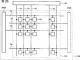
近几年,随着诸如液晶电视的大型显示设备的增加,显示设备得到了积极的发展。具体地讲,由于通过使用由非晶半导体(以下也称为非晶硅)形成的晶体管在同一绝缘基底上方形成像素电路和包括移位寄存器等的驱动器电路(以下也称为内部电路)的技术极大地促进了低功耗和低成本,所以该技术得到了积极的发展。在绝缘基底上方形成的内部电路通过FPC等连接至控制器IC等(以下也称为外部电路),该内部电路的操作受到控制。In recent years, with the increase of large-scale display devices such as liquid crystal televisions, display devices have been actively developed. Specifically, due to the technique of forming a pixel circuit and a driver circuit including a shift register etc. (hereinafter also referred to as an internal circuit) over the same insulating substrate by using transistors formed of an amorphous semiconductor (hereinafter also referred to as amorphous silicon), Low power consumption and low cost are greatly promoted, so the technology is actively developed. An internal circuit formed over an insulating substrate is connected to a controller IC or the like (hereinafter also referred to as an external circuit) through an FPC or the like, and the operation of the internal circuit is controlled.
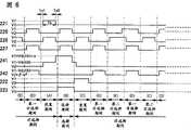
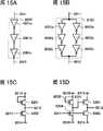
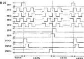
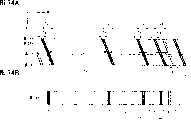
在上述内部电路中设计了通过使用由非晶半导体形成的晶体管(以下也称为非晶晶体管)而形成的移位寄存器。图30A显示包括在传统的移位寄存器中的触发器的结构(参见参考文献1:第2004-157508号日本公布专利申请)。图30A中的触发器包括晶体管11、晶体管12、晶体管13、晶体管14、晶体管15、晶体管16和晶体管17,该触发器连接至信号线21、信号线22、布线23、信号线24、电源线25和电源线26。起始信号、重置信号、时钟信号、电源电位VDD和电源电位VSS分别输入到信号线21、信号线22、信号线24、电源线25和电源线26。如图30B中的时序图所示,图30A中的触发器的操作期间分为设置期间、选择期间、重置期间和非选择期间,大部分操作期间为非选择期间。A shift register formed by using a transistor formed of an amorphous semiconductor (hereinafter also referred to as an amorphous transistor) is designed in the above-described internal circuit. FIG. 30A shows the structure of a flip-flop included in a conventional shift register (see Reference 1: Japanese Laid-Open Patent Application No. 2004-157508). The flip-flop in FIG. 30A includes transistor 11, transistor 12, transistor 13, transistor 14, transistor 15, transistor 16, and transistor 17, and the flip-flop is connected to signal line 21, signal line 22, wiring 23, signal line 24, power supply line 25 and power cord 26. A start signal, a reset signal, a clock signal, a power supply potential VDD, and a power supply potential VSS are input to the signal line 21, the signal line 22, the signal line 24, the power line 25, and the power line 26, respectively. As shown in the timing diagram in FIG. 30B , the operation period of the flip-flop in FIG. 30A is divided into a setting period, a selection period, a reset period and a non-selection period, and most of the operation periods are non-selection periods.
这里,晶体管12和晶体管16在非选择期间中导通。因而,由于非晶硅用于晶体管12和晶体管16中的每个的半导体层,所以由劣化等引起的阈值电压(Vth)波动发生。更具体地讲,阈值电压上升。也就是说,由于阈值电压上升而使得晶体管12和晶体管16中的每个不能导通,所以VSS不能供应给节点41和布线23,传统的移位寄存器发生故障。Here, the transistor 12 and the transistor 16 are turned on during the non-selection period. Thus, since amorphous silicon is used for the semiconductor layer of each of the transistor 12 and the transistor 16, threshold voltage (Vth) fluctuations caused by degradation or the like occur. More specifically, the threshold voltage rises. That is, since each of the transistor 12 and the transistor 16 cannot be turned on because the threshold voltage rises, VSS cannot be supplied to the node 41 and the wiring 23, and the conventional shift register malfunctions.
为了解决这个问题,在参考文献2(Soo Young Yoon等,“HighlyStable Integrated Gate Driver Circuit using a-Si TFT with DualPull-down Structure”,SOCIETY FOR INFORMATION DISPLAY2005 INTERNATIONAL SYMPOSIUM DIGEST OF TECHNICALPAPERS,VolumeXXXVI,pp.348~351)、参考文献3(Binn Kim等,“a-Si Gate Driver Integration with Time Shared Data Driving”,Proceedings of The 12th International Display Workshops inconjunction with Asia Display 2005,pp.1073~1076)和参考文献4(Mindoo Chun等,“Integrated Gate Driver Using Highly Stable a-SiTFT’s”,Proceedings of The 12th International Display Workshops inconj unction with Asia Display 2005,pp.1 077~1 080)中设计了这样的移位寄存器,在该移位寄存器中可抑制晶体管12的阈值电压漂移。在参考文献2、参考文献3和参考文献4中,与晶体管12(描述为第二晶体管)平行地提供新的晶体管(描述为第一晶体管),并且通过在非选择期间中将反相信号输入到第一晶体管的栅极和第二晶体管的栅极来抑制第一晶体管和第二晶体管中的每个的阈值电压漂移。In order to solve this problem, in reference 2 (Soo Young Yoon et al., "HighlyStable Integrated Gate Driver Circuit using a-Si TFT with DualPull-down Structure", SOCIETY FOR INFORMATION DISPLAY2005 INTERNATIONAL SYMPOSIUM DIGEST OF TECHNICALPAPERS, VolumeXXXVI, pp.348~351 ), reference 3 (Binn Kim et al., "a-Si Gate Driver Integration with Time Shared Data Driving", Proceedings of The 12th International Display Workshops inconjunction with Asia Display 2005, pp.1073~1076) and reference 4 (Mindoo Chun et al., "Integrated Gate Driver Using Highly Stable a-SiTFT's", Proceedings of The12th International Display Workshops inconj function with Asia Display 2005, pp.1 077~1 080) designed such a shift register, in which Threshold voltage drift of transistor 12 can be suppressed in the bit register. In
另外,在参考文献5(Chun-Ching等,“Integrated Gate DriverCircuit Using a-Si TFT”,Proceedings of The 12th InternationalDisplay Workshops in conjunction with Asia Display 2005,pp.1023~1026)中设计了这样的移位寄存器,在该移位寄存器中,不仅可抑制晶体管12的阈值电压漂移,而且可抑制晶体管16的阈值电压漂移。在参考文献5中,与晶体管12(描述为第二晶体管)平行地提供新的晶体管(描述为第一晶体管),与晶体管16(描述为第四晶体管)平行地提供新的晶体管(描述为第三晶体管)。然后,通过在非选择期间中将信号输入到第一晶体管的栅极、将反相信号输入到第二晶体管的栅极以及将信号输入到第三晶体管的栅极、将反相信号输入到第四晶体管的栅极,来抑制第一晶体管、第二晶体管、第三晶体管和第四晶体管中的每个的阈值电压漂移。In addition, such a shift is designed in Reference 5 (Chun-Ching et al., "Integrated Gate Driver Circuit Using a-Si TFT", Proceedings of The 12th International Display Workshops in junction with Asia Display 2005, pp. 1023~1026) In this shift register, not only the threshold voltage drift of the transistor 12 but also the threshold voltage drift of the transistor 16 can be suppressed. In Reference 5, a new transistor (described as first transistor) is provided in parallel with transistor 12 (described as second transistor), and a new transistor (described as first transistor) is provided in parallel with transistor 16 (described as fourth transistor). three transistors). Then, by inputting a signal to the gate of the first transistor, inputting an inverted signal to the gate of the second transistor, and inputting a signal to the gate of the third transistor, inputting the inverted signal to the gate of the first transistor during the non-selection period The gates of the four transistors are used to suppress the threshold voltage shift of each of the first transistor, the second transistor, the third transistor and the fourth transistor.
此外,在参考文献6(Young Ho Jang等,“A-Si TFT IntegratedGate Driver with AC-Driven Single Pull-down Structure”,SOCIETYFOR INFORMATION DISPLAY 2006 INTERNATIONALSYMPOSIUM DIGEST OF TECHNICAL PAPERS,Volume XXXVII,pp.208~211)中,通过将AC脉冲施加到晶体管12的栅极来抑制晶体管12的阈值电压漂移。In addition, in reference 6 (Young Ho Jang et al., "A-Si TFT Integrated Gate Driver with AC-Driven Single Pull-down Structure", SOCIETYFOR INFORMATION DISPLAY 2006 INTERNATIONALSYMPOSIUM DIGEST OF TECHNICAL PAPERS, Volume XXXVII, pp. 208-21) , the threshold voltage drift of transistor 12 is suppressed by applying an AC pulse to the gate of transistor 12 .
注意到,对于参考文献7(Jin Young Chio等,“A Compact andCost-efficient TFT-LCD through the Triple-Gate Pixel Structure”,SOCIETY FOR INFORMATION DISPLAY 2006INTERNATIONAL SYMPOSIUM DIGEST OF TECHNICALPAPERS,Volume XXXVII,pp.274~276)和参考文献8(Yong SoonLee等,“Advanced TFT-LCD Data Line Reduction Method”,SOCIETY FOR INFORMATION DISPLAY 2006INTERNATIONAL SYMPOSIUM DIGEST OF TECHNICALPAPERS,Volume XXXVII,pp.1083~1086)中的显示设备中的每个,通过使用利用非晶硅晶体管形成的移位寄存器作为扫描线驱动器电路并将视频信号从一条信号线输入到R、G和B的子像素中的每个来将信号线的数量减少到三分之一。在参考文献7和参考文献8中的显示设备中的每个中,减少了显示面板和驱动器IC的连接的数量。Note that for reference 7 (Jin Young Chio et al., "A Compact and Cost-efficient TFT-LCD through the Triple-Gate Pixel Structure", SOCIETY FOR INFORMATION DISPLAY 2006 INTERNATIONAL SYMPOSIUM DIGEST OF TECHNICALPAPERS, Volume XXXVII, pp 27.674) and each of the display devices in reference 8 (Yong SoonLee et al., "Advanced TFT-LCD Data Line Reduction Method", SOCIETY FOR INFORMATION DISPLAY 2006 INTERNATIONAL SYMPOSIUM DIGEST OF TECHNICALPAPERS, Volume XXXVII, pp.1083~1086), by using The number of signal lines is reduced to one-third using a shift register formed of amorphous silicon transistors as a scan line driver circuit and inputting a video signal from one signal line to each of sub-pixels of R, G, and B. In each of the display devices in Reference 7 and Reference 8, the number of connections of the display panel and the driver IC is reduced.
发明内容Contents of the invention
根据传统技术,通过将AC脉冲施加到容易劣化的晶体管的栅极来抑制该晶体管的阈值电压漂移。然而,在非晶硅用于晶体管的半导体层的情况下,自然地,问题变为形成产生AC脉冲的电路的晶体管的阈值电压漂移发生。According to a conventional technique, threshold voltage drift of a transistor that is prone to deterioration is suppressed by applying an AC pulse to the gate of the transistor. However, in the case where amorphous silicon is used for the semiconductor layer of the transistor, naturally, a problem becomes that the threshold voltage drift of the transistor forming the circuit generating the AC pulse occurs.
另外,虽然已提出通过将信号线的数量减少到三分之一来减少显示面板和驱动器IC的连接的数量(见参考文献7和参考文献8),但是实际上要求与驱动器IC的连接的数量的进一步减少。In addition, although it has been proposed to reduce the number of connections between the display panel and the driver IC by reducing the number of signal lines to one-third (see reference 7 and reference 8), the number of connections to the driver IC is actually required further reduction.
也就是说,作为传统技术没有解决的问题,还留有用于控制晶体管的阈值电压波动的电路技术问题、用于减少安装在显示面板上的驱动器IC的连接数量的技术问题、显示设备的功耗减少的问题以及显示设备的尺寸和高清晰度的增加的问题。That is, as problems not solved by the conventional technology, there remain circuit technical problems for controlling fluctuations in the threshold voltage of transistors, technical problems for reducing the number of connections of driver ICs mounted on a display panel, power consumption of a display device, etc. The problem of reduction and the problem of increase in size and high definition of display devices.
该说明书中所公开的本发明的目的在于通过解决前述问题中的一个问题或多个问题来提供工业上有益的技术。The present invention disclosed in this specification aims to provide an industrially useful technique by solving one or more of the aforementioned problems.
在根据本发明的显示设备中,可通过将正电源和负电源交替施加到容易劣化的晶体管的栅极来抑制该晶体管的阈值电压漂移。In the display device according to the present invention, it is possible to suppress threshold voltage shift of a transistor which is easily deteriorated by alternately applying positive power and negative power to the gate of the transistor.
另外,在根据本发明的显示设备中,可通过经由开关将高电位(VDD)和低电位(VSS)交替施加到容易劣化的晶体管的栅极来抑制该晶体管的阈值电压漂移。In addition, in the display device according to the present invention, threshold voltage drift of a transistor that is easily deteriorated can be suppressed by alternately applying high potential (VDD) and low potential (VSS) to the gate of the transistor through a switch.
具体地讲,容易劣化的晶体管的栅极连接至高电位通过第一开关晶体管供应给其的布线和低电位通过第二开关晶体管供应给其的布线;时钟信号输入到第一开关晶体管的栅极;反向时钟信号输入第二开关晶体管的栅极。因而,高电位和低电位交替施加到容易劣化的晶体管的栅极。Specifically, the gate of the transistor prone to deterioration is connected to a wiring to which a high potential is supplied through the first switching transistor and a wiring to which a low potential is supplied through the second switching transistor; a clock signal is input to the gate of the first switching transistor; The reverse clock signal is input to the gate of the second switching transistor. Thus, high potentials and low potentials are alternately applied to the gates of transistors that are prone to deterioration.
应该指出,各种类型的开关可用作该文档(说明书、权利要求、附图等)中所示的开关。作为示例给出电开关、机械开关等。也就是说,可使用任何元件,只要它可控制电流即可,而不限于某个元件。例如,晶体管(比如,双极性晶体管或MOS晶体管)、二极管(比如,PN二极管、PIN二极管、肖特基二极管、MIM(金属绝缘体金属)二极管、MIS(金属绝缘体半导体)二极管或二极管连接的晶体管)、晶闸管等可用作开关。可选地,将这样的元件组合在一起的逻辑电路可用作开关。It should be noted that various types of switches can be used as the switches shown in this document (specification, claims, drawings, etc.). An electric switch, a mechanical switch, and the like are given as examples. That is, any element can be used as long as it can control the current without being limited to a certain element. For example, transistors (such as bipolar transistors or MOS transistors), diodes (such as PN diodes, PIN diodes, Schottky diodes, MIM (metal insulator metal) diodes, MIS (metal insulator semiconductor) diodes, or diode-connected transistors ), thyristors, etc. can be used as switches. Alternatively, a logic circuit combining such elements may be used as a switch.
在使用晶体管作为开关的情况下,由于晶体管仅作为开关操作,所以不特别限制晶体管的极性(传导类型)。然而,当将抑制截止电流时,优选使用具有较小截止电流的极性的晶体管。作为具有较小截止电流的晶体管的示例,给出提供有LDD区的晶体管、具有多栅结构的晶体管等。另外,优选地,当作为开关操作的晶体管的源端子的电位更接近低电位侧电源(比如,Vss、GND或0V)时,使用N沟道晶体管,而当源端子的电位更接近高电位侧电源(比如,Vdd)时,使用P沟道晶体管。这是因为:在N沟道晶体管中当作为开关操作的晶体管的源端子的电位更接近低电位侧电源时,以及在P沟道晶体管中当作为开关操作的晶体管的源端子的电位更接近高电位侧电源时,可增加栅源电压的绝对值,从而该晶体管可更精确地作为开关操作。这还因为:不经常执行源跟随器操作,从而输出电压的减小不经常发生。In the case of using a transistor as a switch, since the transistor operates only as a switch, the polarity (conduction type) of the transistor is not particularly limited. However, when off-current is to be suppressed, it is preferable to use a transistor having a polarity of smaller off-current. As examples of a transistor having a small off-current, a transistor provided with an LDD region, a transistor having a multi-gate structure, and the like are given. In addition, it is preferable to use an N-channel transistor when the potential of the source terminal of a transistor operating as a switch is closer to a low-potential side power supply (for example, Vss, GND, or 0 V), and when the potential of the source terminal is closer to the high-potential side For power supply (for example, Vdd), use P-channel transistors. This is because when the potential of the source terminal of the transistor operating as a switch is closer to the low-potential side power supply in an N-channel transistor, and when the potential of the source terminal of a transistor operating as a switch is closer to a high potential in a P-channel transistor When the potential side is powered, the absolute value of the gate-source voltage can be increased so that the transistor can operate more precisely as a switch. This is also because the source follower operation is performed infrequently, and thus the reduction in output voltage does not occur frequently.
应该指出,可通过使用N沟道晶体管和P沟道晶体管来采用CMOS开关。通过采用CMOS开关,由于当P沟道晶体管或N沟道晶体管导通时电流可流动,所以该开关可更精确地作为开关操作。例如,无论开关的输入信号的电压是高还是低,都可适当地输出电压。另外,由于可使用于开启或关闭开关的信号的电压幅值变小,所以可减少功耗。It should be noted that CMOS switches can be employed by using N-channel transistors and P-channel transistors. By employing a CMOS switch, since a current can flow when a P-channel transistor or an N-channel transistor is turned on, the switch can be operated more precisely as a switch. For example, regardless of whether the voltage of the input signal of the switch is high or low, the voltage can be appropriately output. In addition, since the voltage amplitude of a signal for turning on or off a switch can be made small, power consumption can be reduced.
还应该指出,当晶体管用作开关时,该开关包括输入端子(源端子和漏端子中的一个)、输出端子(源端子和漏端子中的另一个)和用于控制电传导的端子(栅极)。另一方面,当二极管用作开关时,在一些情况下,该开关不具有用于控制电传导的端子。因此,当二极管用作开关时,可比使用晶体管作为开关的情况更多地减少用于控制端子的布线的数量。It should also be noted that when a transistor is used as a switch, the switch includes an input terminal (one of source and drain terminals), an output terminal (the other of source and drain terminals), and a terminal for controlling electrical conduction (gate pole). On the other hand, when a diode is used as a switch, in some cases, the switch does not have a terminal for controlling electrical conduction. Therefore, when a diode is used as a switch, the number of wirings for the control terminal can be reduced more than in the case of using a transistor as a switch.
应该指出,在该说明书中,当明确地描述“A和B连接”时,元件电连接的情况、元件在功能上连接的情况和元件直接连接的情况包括在其中。这里,A和B中的每个对应于物体(比如,设备、元件、电路、布线、电极、端子、传导膜或层)。因此,在该说明书中所公开的结构中,另一元件可插在具有附图和文本中所示的连接关系的元件之间,所述连接关系不限于预定的连接关系,例如,附图和文本中所示的连接关系。It should be noted that in this specification, when "A and B are connected" is explicitly described, the case where elements are electrically connected, the case where elements are functionally connected, and the case where elements are directly connected are included therein. Here, each of A and B corresponds to an object (eg, device, element, circuit, wiring, electrode, terminal, conductive film or layer). Therefore, in the structure disclosed in this specification, another element may be inserted between the elements having the connection relationship shown in the drawings and the text, the connection relationship is not limited to the predetermined connection relationship, for example, the drawings and Connections shown in the text.
例如,在A和B电连接的情况下,可在A和B之间提供能够实现A和B的电连接的一个或多个元件(比如,开关、晶体管、电容器、感应器、电阻器和/或二极管)。另外,在A和B在功能上连接的情况下,可在A和B之间提供能够实现A和B的功能连接的一个或多个电路(比如,逻辑电路、信号转换器电路、电位电平转换器电路、信号发生电路、存储器电路和/或控制电路,所述逻辑电路诸如反相器、NAND电路或NOR电路,所述信号转换器电路诸如DA转换器电路、AD转换器电路或伽马校正电路,所述电位电平转换器电路诸如电源电路(比如,提升电路或压降控制电路)或用于改变信号、电压源、电流源的电位电平的电平转换器电路、开关电路或放大器电路,所述放大器电路诸如可增加信号幅度、电流量等的电路(比如,运算放大器、差动放大器电路、源跟随器电路或缓冲器电路)。可选地,在A和B直接连接的情况下,A和B可直接连接,而不在A和B之间插入另一元件或另一电路。For example, where A and B are electrically connected, one or more elements (such as switches, transistors, capacitors, inductors, resistors, and/or or diode). In addition, in the case where A and B are functionally connected, one or more circuits (such as logic circuits, signal converter circuits, potential level A converter circuit, a signal generating circuit, a memory circuit and/or a control circuit, the logic circuit such as an inverter, a NAND circuit or a NOR circuit, the signal converter circuit such as a DA converter circuit, an AD converter circuit or a gamma Correction circuits, said potential level shifter circuits such as power supply circuits (for example, boost circuits or voltage drop control circuits) or level shifter circuits for changing the potential levels of signals, voltage sources, current sources, switching circuits or An amplifier circuit such as a circuit that can increase signal amplitude, current flow, etc. (for example, an operational amplifier, a differential amplifier circuit, a source follower circuit, or a buffer circuit). Optionally, between A and B directly connected case, A and B can be directly connected without interposing another element or another circuit between A and B.
应该指出,当明确地描述“A和B直接连接”时,A和B直接连接的情况(即,A和B直接连接,而不在A和B之间插入另一元件或另一电路的情况)以及A和B电连接的情况(即,通过在A和B之间插入另一元件或另一电路来连接A和B的情况)包括在其中。It should be noted that when "A and B are directly connected" is explicitly described, the case where A and B are directly connected (that is, the case where A and B are directly connected without interposing another element or another circuit between A and B) And a case where A and B are electrically connected (ie, a case where A and B are connected by interposing another element or another circuit between A and B) is included therein.
应该指出,当明确地描述“A和B电连接”时,A和B电连接的情况(即,通过在A和B之间插入另一元件或另一电路来连接A和B的情况)、A和B在功能上连接的情况(即,通过在A和B之间插入另一电路来从功能上连接A和B的情况)以及A和B直接连接的情况(即,A和B连接,而不在A和B之间插入另一元件或另一电路的情况)包括在其中。也就是说,当明确地描述“A和B电连接”时,描述与仅明确地描述“A和B连接”的情况相同。It should be noted that when "A and B are electrically connected" is explicitly described, the case where A and B are electrically connected (that is, the case where A and B are connected by interposing another element or another circuit between A and B), The case where A and B are functionally connected (that is, the case where A and B are functionally connected by inserting another circuit between A and B) and the case where A and B are directly connected (that is, A and B are connected, A case where another element or another circuit is not inserted between A and B) is included therein. That is, when "A and B are electrically connected" is explicitly described, the description is the same as the case where only "A and B are connected" is explicitly described.
应该指出,显示元件、作为具有显示元件的设备的显示设备、发光元件、作为具有发光元件的设备的发光设备可采用各种类型,并且可包括各种元件。例如,作为其显示介质、对比度、亮度、反射性、透射性等根据电磁反应而改变的显示元件、显示设备、发光元件和发光设备,可采用诸如EL元件(比如,有机EL元件、无机EL元件或包括有机材料和无机材料的EL元件)、电子发射器、液晶元件、电子墨、电泳元件、光栅光阀(GLV)、等离子体显示面板(PDP)、数字微镜设备(DMD)、压电陶瓷显示器或碳纳米管。应该指出,使用EL元件的显示设备包括EL显示器;使用电子发射器的显示设备包括场发射显示器(FED)、SED型平板显示器(SED:表面传导电子发射器显示器)等;使用液晶元件的显示设备包括液晶显示器(比如,透射液晶显示器、半透射液晶显示器、反射液晶显示器、直接观看液晶显示器或投影液晶显示器);使用电子墨的显示设备包括电子纸。It should be noted that the display element, the display device as a device having a display element, the light emitting element, and the light emitting device as a device having a light emitting element may take various types, and may include various elements. For example, as a display element, a display device, a light-emitting element, and a light-emitting device whose display medium, contrast, brightness, reflectivity, transmittance, etc. change according to electromagnetic reactions, such as EL elements (such as organic EL elements, inorganic EL elements, etc. or EL elements including organic materials and inorganic materials), electron emitters, liquid crystal elements, electronic ink, electrophoretic elements, grating light valves (GLV), plasma display panels (PDP), digital micromirror devices (DMD), piezoelectric Ceramic displays or carbon nanotubes. It should be noted that display devices using EL elements include EL displays; display devices using electron emitters include field emission displays (FED), SED-type flat panel displays (SED: Surface Conduction Electron Emitter Display), etc.; display devices using liquid crystal elements Includes liquid crystal displays (eg, transmissive liquid crystal displays, transmissive liquid crystal displays, reflective liquid crystal displays, direct view liquid crystal displays, or projection liquid crystal displays); display devices that use electronic ink include electronic paper.
应该指出,在该文档(说明书、权利要求、附图等)中,各种类型的晶体管可用作晶体管,而不限于某种类型。例如,可采用包括非单晶半导体膜的薄膜晶体管(TFT),非晶硅、多晶硅、微晶(也称为半非晶)硅等为非单晶半导体的类型。在使用TFT的情况下,存在各种优点。例如,由于可在比使用单晶硅的情况下的温度低的温度下形成TFT,所以可降低制造成本,并且可使制造设备做得较大。由于可使制造设备做得较大,所以可使用大的基底形成TFT。因此,由于可同时形成许多显示设备,所以可以以低成本形成TFT。另外,由于制造温度低,所以可使用具有低耐热性的基底。因此,可在透光基底上方形成晶体管。此外,可通过使用在透光基底上方形成的晶体管来控制显示元件中的光的透射。可选地,由于晶体管的膜厚度薄,所以膜的形成晶体管的部分可透射光。因此,可改进开口率。It should be noted that in this document (specification, claims, drawings, etc.), various types of transistors can be used as transistors without being limited to a certain type. For example, a thin film transistor (TFT) including a non-single crystal semiconductor film, amorphous silicon, polycrystalline silicon, microcrystalline (also referred to as semi-amorphous) silicon, etc. as types of non-single crystal semiconductors can be employed. In the case of using TFTs, there are various advantages. For example, since TFTs can be formed at a temperature lower than that in the case of using single-crystal silicon, manufacturing costs can be reduced, and manufacturing equipment can be made larger. Since the manufacturing equipment can be made larger, TFTs can be formed using a large substrate. Therefore, since many display devices can be formed at the same time, TFTs can be formed at low cost. In addition, since the manufacturing temperature is low, a substrate with low heat resistance can be used. Accordingly, transistors can be formed over the light-transmitting substrate. In addition, the transmission of light in the display element can be controlled by using transistors formed over the light-transmitting substrate. Alternatively, since the film thickness of the transistor is thin, the portion of the film where the transistor is formed can transmit light. Therefore, the aperture ratio can be improved.
应该指出,通过在形成多晶硅的情况下使用催化剂(比如,镍),可进一步改进结晶性,并且可形成具有优良的电特性的晶体管。因此,可在同一基底上方形成栅驱动器电路(比如,扫描线驱动器电路)、源驱动器电路(比如,信号线驱动器电路)和信号处理电路(比如,信号产生电路、伽马校正电路或DA转换器电路)。It should be noted that by using a catalyst such as nickel in the case of forming polysilicon, crystallinity can be further improved, and a transistor having excellent electrical characteristics can be formed. Therefore, a gate driver circuit (such as a scan line driver circuit), a source driver circuit (such as a signal line driver circuit), and a signal processing circuit (such as a signal generation circuit, a gamma correction circuit, or a DA converter circuit) can be formed over the same substrate. circuit).
应该指出,通过在形成微晶硅的情况下使用催化剂(比如,镍),可进一步改进结晶性,并且可形成具有优良的电特性的晶体管。此时,可通过执行热处理而不使用激光来改进结晶性。因此,可在同一基底上方形成栅驱动器电路(比如,扫描线驱动器电路)和源驱动器电路的一部分(比如,模拟开关)。另外,在不使用激光用于结晶的情况下,可抑制硅的结晶不匀。因此,可显示具有高图像质量的图像。It should be noted that by using a catalyst such as nickel in the case of forming microcrystalline silicon, crystallinity can be further improved, and a transistor having excellent electrical characteristics can be formed. At this time, crystallinity can be improved by performing heat treatment without using laser light. Accordingly, a gate driver circuit (eg, a scan line driver circuit) and a part of a source driver circuit (eg, an analog switch) can be formed over the same substrate. In addition, crystallization unevenness of silicon can be suppressed without using laser light for crystallization. Therefore, images with high image quality can be displayed.
还应该指出,可不使用催化剂(比如,镍)形成多晶硅和微晶硅。It should also be noted that polysilicon and microcrystalline silicon can be formed without the use of a catalyst (eg, nickel).
另外,可通过使用半导体基底、SOI基底等形成晶体管。在这种情况下,MOS晶体管、结型晶体管、双极晶体管等可用作该说明书中描述的晶体管。因此,可形成特性、尺寸、形状等变化小、电流供应性能高且尺寸小的晶体管。通过使用这样的晶体管,可减少电路的功耗,或者可高度集成电路。In addition, a transistor can be formed by using a semiconductor substrate, an SOI substrate, or the like. In this case, MOS transistors, junction transistors, bipolar transistors, and the like can be used as the transistors described in this specification. Therefore, it is possible to form a transistor having small variations in characteristics, size, shape, etc., high current supply performance, and small size. By using such transistors, power consumption of the circuit can be reduced, or highly integrated circuits can be achieved.
另外,可使用包括化合半导体或氧化物半导体的晶体管和通过使这样的化合半导体或氧化物半导体变薄而获得的薄膜晶体管等,所述氧化物半导体诸如ZnO、a-InGaZnO、SiGe、GaAs、IZO、ITO(氧化铟锡)或SnO。因此,可降低制造温度,例如,可在室温下形成这样的晶体管。因此,可在具有低耐热性的基底,诸如塑料基底或膜基底上直接形成晶体管。应该指出,这样的化合半导体或氧化物半导体不仅可用于晶体管的沟道部分,而且还可用于其它应用。例如,这样的化合半导体或氧化物半导体可用作电阻器、像素电极或透光电极。此外,由于可在与晶体管相同的时间形成这样的元件,所以可降低成本。In addition, a transistor including a compound semiconductor or an oxide semiconductor such as ZnO, a-InGaZnO, SiGe, GaAs, IZO, etc., and a thin film transistor obtained by thinning such a compound semiconductor or an oxide semiconductor can be used. , ITO (indium tin oxide) or SnO. Therefore, the fabrication temperature can be lowered, for example, such transistors can be formed at room temperature. Accordingly, transistors can be directly formed on a substrate having low heat resistance, such as a plastic substrate or a film substrate. It should be noted that such compound semiconductors or oxide semiconductors can be used not only for channel portions of transistors but also for other applications. For example, such a compound semiconductor or an oxide semiconductor can be used as a resistor, a pixel electrode, or a light-transmitting electrode. In addition, since such elements can be formed at the same time as transistors, cost can be reduced.
还可使用通过使用喷墨法或印刷法而形成的晶体管等。因此,可在室温下形成这样的晶体管,可在低真空下形成这样的晶体管,或者可使用大的基底形成这样的晶体管。另外,由于可不使用掩模(分划板)形成晶体管,所以可容易改变晶体管的布局。此外,由于没有必要使用抗蚀剂,所以降低材料成本,并且可降低步骤的数量。再者,由于仅在必要的部分中形成膜,所以与在整个表面上方形成膜之后执行蚀刻的制造方法相比,没有浪费材料,从而可降低成本。A transistor or the like formed by using an inkjet method or a printing method can also be used. Accordingly, such transistors may be formed at room temperature, may be formed under low vacuum, or may be formed using a large substrate. In addition, since the transistors can be formed without using a mask (reticle), the layout of the transistors can be easily changed. In addition, since it is not necessary to use a resist, material costs are reduced, and the number of steps can be reduced. Also, since the film is formed only in necessary portions, compared with a manufacturing method in which etching is performed after forming a film over the entire surface, no material is wasted, so that cost can be reduced.
此外,可使用包括有机半导体或碳纳米管的晶体管等。因此,可使用可弯曲的基底形成这样的晶体管。因此,晶体管可抵抗冲击。In addition, transistors including organic semiconductors or carbon nanotubes, etc. may be used. Accordingly, such transistors can be formed using bendable substrates. Therefore, the transistor is resistant to shocks.
再者,可使用各种晶体管。Also, various transistors can be used.
而且,可使用各种类型的基底形成晶体管。基底的类型不限于某种类型。例如,单晶硅、SOI基底、玻璃基底、石英基底、塑料基底、纸质基底、玻璃纸质基底、石质基底、木质基底、布质基底(包括天然纤维(比如,丝、棉或大麻纤维)、合成纤维(比如,尼龙、聚氨酯或涤纶)、再生纤维(比如,醋酸纤维、铜氨纤维、人造纤维或再生涤纶)等)、皮质基底、橡胶基底、不锈钢基底、包括不锈钢箔的基底等可用作基底。可选地,动物,诸如人类的皮肤(比如,表皮或真皮)或者皮下组织可用作基底。另外,可使用一个基底形成晶体管,然后,可将该晶体管传送到另一基底。单晶硅基底、SOI基底、玻璃基底、石英基底、塑料基底、纸质基底、玻璃纸质基底、石质基底、木质基底、布质基底(包括天然纤维(比如,丝、棉或大麻纤维)、合成纤维(比如,尼龙、聚氨酯或涤纶)、再生纤维(比如,醋酸纤维、铜氨纤维、人造纤维或再生涤纶)等)、皮质基底、橡胶基底、不锈钢基底、包括不锈钢箔的基底等可用作将所述晶体管传送至其的基底。可选地,动物,诸如人类的皮肤(比如,表皮或真皮)或者皮下组织可用作将所述晶体管传送至其的基底。通过使用这样的基底,可形成具有优良属性的晶体管或具有低功耗的晶体管,可形成具有高耐用性或高耐热性的设备,或者可实现重量的减轻。Also, various types of substrates may be used to form transistors. The type of base is not limited to a certain type. For example, monocrystalline silicon, SOI substrates, glass substrates, quartz substrates, plastic substrates, paper substrates, cellophane substrates, stone substrates, wood substrates, cloth substrates (including natural fibers such as silk, cotton, or hemp ), synthetic fibers (such as nylon, polyurethane or polyester), recycled fibers (such as acetate, cupro, rayon or recycled polyester), etc.), leather substrates, rubber substrates, stainless steel substrates, substrates including stainless steel foil, etc. Can be used as a base. Alternatively, the skin (eg, epidermis or dermis) or subcutaneous tissue of an animal, such as a human, can be used as a substrate. In addition, one substrate can be used to form a transistor, which can then be transferred to another substrate. Monocrystalline silicon substrates, SOI substrates, glass substrates, quartz substrates, plastic substrates, paper substrates, cellophane substrates, stone substrates, wood substrates, cloth substrates (including natural fibers such as silk, cotton, or hemp) , synthetic fibers (such as nylon, polyurethane, or polyester), recycled fibers (such as acetate, cupro, rayon, or recycled polyester), etc.), leather substrates, rubber substrates, stainless steel substrates, substrates including stainless steel foil, etc. Serves as the substrate to which the transistors are transferred. Alternatively, the skin (eg, epidermis or dermis) or subcutaneous tissue of an animal, such as a human, can be used as a substrate to which the transistor is delivered. By using such a substrate, a transistor with excellent properties or a transistor with low power consumption can be formed, a device with high durability or high heat resistance can be formed, or weight reduction can be achieved.
晶体管的结构可以是各种模式,不限于某种结构。例如,可使用具有两个或多个栅极的多栅结构。当使用多栅结构时,由于提供沟道区串联的结构,所以提供多个晶体管串联的结构。通过使用多栅结构,可减小截止电流或者可增加晶体管的耐压以提高可靠性。可选地,通过使用多栅结构,当晶体管在饱和区中操作时,即使漏源电压波动,漏源电流也不会波动太多,从而可获得平缓坡度的电压-电流特性。通过利用平缓坡度的电压-电流特性,可实现理想的电流源电路或具有高阻抗值的有源负载。因此,可实现具有优良属性的差动电路或电流镜像电路。另外,可使用在沟道上方和沟道下方形成栅极的结构。通过使用在沟道上方和沟道下方形成栅极的结构,沟道区扩大,从而可增加流过沟道区的电流量或者可容易形成耗尽层以降低S值。当在沟道上方和沟道下方形成栅极时,提供多个晶体管并联的结构。The structure of the transistor can be in various modes and is not limited to a certain structure. For example, a multi-gate structure with two or more gates can be used. When a multi-gate structure is used, since a structure in which channel regions are connected in series is provided, a structure in which a plurality of transistors are connected in series is provided. By using a multi-gate structure, off-current can be reduced or the withstand voltage of a transistor can be increased to improve reliability. Alternatively, by using a multi-gate structure, when the transistor operates in a saturation region, even if the drain-source voltage fluctuates, the drain-source current does not fluctuate so much, so that a gentle-slope voltage-current characteristic can be obtained. By utilizing the gently sloped voltage-current characteristics, ideal current source circuits or active loads with high impedance values can be realized. Therefore, a differential circuit or a current mirror circuit having excellent properties can be realized. In addition, a structure in which gates are formed above and below the channel may be used. By using a structure in which gates are formed above and below the channel, the channel region is enlarged so that the amount of current flowing through the channel region can be increased or a depletion layer can be easily formed to lower the S value. When gates are formed above and below the channel, a structure in which multiple transistors are connected in parallel is provided.
此外,可采用在沟道上方形成栅极的结构、在沟道下方形成栅极的结构、交错结构、反交错结构、沟道区分为多个区的结构或者沟道区并联或串联的结构。另外,源极或漏极可与沟道区(或其一部分)重叠。通过使用源极或漏极可与沟道区(或其一部分)重叠的结构,可防止电荷在沟道区的一部分中累积的情况,电荷在沟道区的一部分中累积可导致不稳定的操作。此外,可提供LDD区。通过提供LDD区,可降低截止电流或者可增加耐压以提高可靠性。可选地,当晶体管在饱和区中操作时,即使漏源电压波动,漏源电流也不会波动太多,从而可获得平缓坡度的电压-电流特性。In addition, a structure in which a gate is formed above a channel, a structure in which a gate is formed below a channel, a staggered structure, an inverse staggered structure, a structure in which a channel region is divided into a plurality of regions, or a structure in which channel regions are connected in parallel or in series may be employed. Additionally, the source or drain may overlap the channel region (or a portion thereof). By using a structure in which the source or drain can overlap the channel region (or a portion thereof), it is possible to prevent a situation where charges accumulate in a portion of the channel region, which can lead to unstable operation . In addition, an LDD area may be provided. By providing the LDD region, off-current can be reduced or withstand voltage can be increased to improve reliability. Alternatively, when the transistor operates in the saturation region, even if the drain-source voltage fluctuates, the drain-source current does not fluctuate much, so that a gentle slope voltage-current characteristic can be obtained.
应该指出,各种类型的晶体管可用于该说明书中的晶体管,并且可使用各种类型的基底形成晶体管。因此,可使用同一基底形成实现预定功能所需的所有电路。例如,可使用玻璃基底、塑料基底、单晶基底、SOI基底或任何其它基底形成实现预定功能所需的所有电路。当使用同一基底形成实现预定功能所需的所有电路时,可减少组件部分的数量以削减成本,并且可减少与电路组件的连接的数量以提高可靠性。可选地,可使用一个基底形成实现预定功能所需的部分电路,使用另一基底形成实现预定功能所需的另一部分电路。也就是说,不需要使用同一基底形成实现预定功能所需的所有电路。例如,可用使用玻璃基底的晶体管形成实现预定功能所需的部分电路,可使用单晶基底形成实现预定功能所需的另一部分电路,从而可通过COG(芯片被贴装在玻璃基底上)将通过使用单晶基底的晶体管形成的IC芯片与玻璃基底连接,并且可在玻璃基底上方提供IC芯片。可选地,可通过TAB(卷带式自动结合)或印刷布线板将IC芯片与玻璃基底连接。当以这种方式使用同一基底形成所述电路中的部分电路时,可减少组件部分的数量以削减成本,并且可减少与电路组件的连接的数量以提高可靠性。另外,例如,通过使用单晶基底和使用由电路形成的IC芯片形成具有高驱动电压的部分或具有高驱动频率的部分,而不是使用同一基底形成这样的部分,可防止功耗的增加,其中,形成具有高驱动电压的部分或具有高驱动频率的部分耗费大功率。It should be noted that various types of transistors can be used for the transistors in this specification, and various types of substrates can be used to form the transistors. Therefore, all circuits required to realize predetermined functions can be formed using the same substrate. For example, a glass substrate, a plastic substrate, a single crystal substrate, an SOI substrate, or any other substrate may be used to form all the circuits required to realize predetermined functions. When all circuits required to realize predetermined functions are formed using the same substrate, the number of component parts can be reduced to cut costs, and the number of connections to circuit components can be reduced to improve reliability. Alternatively, one substrate may be used to form a part of circuits required to realize predetermined functions, and another substrate may be used to form another part of circuits required to realize predetermined functions. That is, it is not necessary to use the same substrate to form all the circuits necessary to realize the intended function. For example, a part of the circuit required to realize a predetermined function can be formed using a transistor using a glass substrate, and another part of the circuit required to realize a predetermined function can be formed using a single crystal substrate, so that the through An IC chip formed using transistors of a single crystal substrate is connected to a glass substrate, and the IC chip may be provided over the glass substrate. Alternatively, the IC chip may be connected to the glass substrate by TAB (Tape Automated Bonding) or a printed wiring board. When some of the circuits are formed using the same substrate in this way, the number of component parts can be reduced to cut costs, and the number of connections to circuit components can be reduced to improve reliability. In addition, for example, by using a single crystal substrate and forming a portion having a high driving voltage or a portion having a high driving frequency using an IC chip formed of a circuit instead of forming such a portion using the same substrate, an increase in power consumption can be prevented, wherein , forming a portion with a high driving voltage or a portion with a high driving frequency consumes large power.
还应该指出,在该说明书中,一个像素与其亮度可控的一个元件对应。因此,例如,一个像素与一个颜色元件对应,并且用该一个颜色元件表示亮度。因此,在具有R(红)、G(绿)和B(蓝)颜色元件的彩色显示设备的情况下,图像的最小单元由R像素、G像素和B像素三个像素形成。应该指出,颜色元件不限于三种颜色,可使用多于三种颜色的颜色元件,或者可添加不同于RGB的颜色。例如,可通过添加白色使用RGBW(W对应于白色)。另外,可使用RGB加上黄色、青绿色、品红、鲜绿色、朱红色等中的一种或多种颜色。此外,可将与R、G和B中的至少一个类似的颜色添加到RGB中。例如,可使用R、G、B1和B2。虽然B1和B2都是蓝色,但是它们具有稍微不同的频率。类似地,可使用R1、R2、G和B。通过使用这样的颜色元件,可执行更接近实际物体的显示,或者可减少功耗。可选地,作为另一示例,在通过使用多个区来控制一个颜色元件的亮度的情况下,一个区对应于一个像素。因此,例如,在执行面积比率灰阶显示的情况下或者在包括子像素的情况下,在每个颜色元件中提供控制亮度的多个区,并且用整个区表示灰阶。在这种情况下,一个控制亮度的区可对应于一个像素。因而,在这种情况下,一个颜色元件包括多个像素。可选地,即使当在一个颜色元件中提供控制亮度的多个区时,也可将这些区集合为一个像素。因而,在这种情况下,一个颜色元件包括一个像素。在这种情况下,一个颜色元件包括一个像素。在每个颜色元件中的多个区中控制亮度的情况下,在一些情况下,对显示有贡献的区具有取决于像素的不同的面积大小。另外,在每个颜色元件中的控制亮度的多个区中,供应给所述多个区中的每个的信号可以稍微变化以使视角变宽。也就是说,包括在每个颜色元件中提供的所述多个区中的像素电极的电位可以彼此不同。因此,施加到液晶分子的电压根据像素电极而变化。因此,可使视角变宽。It should also be noted that in this specification, one pixel corresponds to one element whose brightness is controllable. Therefore, for example, one pixel corresponds to one color element, and brightness is expressed with this one color element. Therefore, in the case of a color display device having R (red), G (green), and B (blue) color elements, the minimum unit of an image is formed by three pixels of R pixel, G pixel, and B pixel. It should be noted that the color elements are not limited to three colors, color elements of more than three colors may be used, or colors other than RGB may be added. For example, RGBW can be used by adding white (W corresponds to white). In addition, RGB plus one or more colors of yellow, cyan, magenta, emerald green, vermilion, etc. may be used. Also, a color similar to at least one of R, G, and B may be added to RGB. For example, R, G, B1 and B2 can be used. Although both B1 and B2 are blue, they have slightly different frequencies. Similarly, R1, R2, G and B can be used. By using such color elements, display closer to an actual object can be performed, or power consumption can be reduced. Alternatively, as another example, in the case of controlling the brightness of one color element by using a plurality of areas, one area corresponds to one pixel. Therefore, for example, in the case of performing area ratio gradation display or in the case of including sub-pixels, a plurality of areas for controlling luminance are provided in each color element, and gradation is expressed with the entire area. In this case, one area for controlling brightness may correspond to one pixel. Thus, in this case, one color element includes a plurality of pixels. Alternatively, even when a plurality of areas for controlling luminance are provided in one color element, these areas may be aggregated into one pixel. Thus, in this case, one color element includes one pixel. In this case, one color element includes one pixel. In the case of controlling luminance in a plurality of regions in each color element, regions contributing to display have different area sizes depending on pixels in some cases. In addition, in a plurality of regions controlling luminance in each color element, a signal supplied to each of the plurality of regions may be slightly changed to widen the viewing angle. That is, potentials of pixel electrodes included in the plurality of regions provided in each color element may be different from each other. Therefore, the voltage applied to the liquid crystal molecules varies according to the pixel electrodes. Therefore, the viewing angle can be widened.
应该指出,当明确地描述“一个像素三种颜色”时,它与认为R、G和B三个像素为一个像素的情况对应。同时,当明确地描述“一个像素一种颜色”时,它与在每个颜色元件中提供多个区并且将所述多个区共认为是一个像素的情况对应。It should be noted that when "three colors for one pixel" is explicitly described, it corresponds to the case where three pixels of R, G, and B are regarded as one pixel. Meanwhile, when "one pixel one color" is explicitly described, it corresponds to a case where a plurality of regions are provided in each color element and the plurality of regions are collectively considered as one pixel.
还应该指出,在该文档(说明书、权利要求、附图等)中,在一些情况下按矩阵布置(提供)像素。这里,按矩阵布置(提供)像素的描述包括按直线布置像素的情况以及按纵向或横向的锯齿形线布置像素的情况。因此,在用三种颜色元件(比如,RGB)执行完全颜色显示的情况下,以下情况包括在其中:按条纹布置像素的情况和按delta图案布置三种颜色元件的点的情况。另外,按Bayer排列提供三种颜色元件的点的情况也包括在其中。应该指出,颜色元件不限于三种颜色,可采用多于三种颜色的颜色元件。作为示例给出RGBW(W对应于白色)、RGB加上黄色、青绿色、品红等中的一个或多个。此外,颜色元件的各点之间显示区域的大小可不同。因而,可减小功耗,并且可延长显示元件的寿命。It should also be noted that in this document (specification, claims, drawings, etc.), pixels are arranged (provided) in a matrix in some cases. Here, the description of arranging (providing) pixels in a matrix includes a case of arranging pixels in a straight line and a case of arranging pixels in zigzag lines in a longitudinal or lateral direction. Therefore, in the case of performing full color display with three color elements such as RGB, the following cases are included: a case of arranging pixels in stripes and a case of arranging dots of three color elements in a delta pattern. In addition, a case where dots of three color elements are provided in a Bayer arrangement is also included. It should be noted that the color elements are not limited to three colors, and color elements of more than three colors may be used. One or more of RGBW (W corresponds to white), RGB plus yellow, cyan, magenta, etc. are given as examples. In addition, the size of the display area may vary between dots of a color element. Thus, power consumption can be reduced, and the lifetime of the display element can be extended.
还应该指出,在该文档(说明书、权利要求、附图等)中,可使用有源元件包括在像素中的有源矩阵法或有源元件不包括在像素中的无源矩阵法。It should also be noted that in this document (specification, claims, drawings, etc.), an active matrix method in which an active element is included in a pixel or a passive matrix method in which an active element is not included in a pixel may be used.
在有源矩阵法中,作为有源元件(非线性元件),不仅可使用晶体管,而且还可使用各种有源元件(非线性元件)。例如,还可使用MIM(金属绝缘体金属)、TFD(薄膜二极管)等。由于这样的元件具有很少的制造步骤,所以可降低制造成本,或者可提高产量。此外,由于元件的尺寸小,所以可改进开口率,从而可减小功耗,或者可实现高亮度。In the active matrix method, not only transistors but various active elements (nonlinear elements) can be used as active elements (nonlinear elements). For example, MIM (Metal Insulator Metal), TFD (Thin Film Diode), and the like can also be used. Since such elements have fewer manufacturing steps, manufacturing costs can be reduced, or yields can be increased. Furthermore, since the size of the element is small, the aperture ratio can be improved, so that power consumption can be reduced, or high brightness can be realized.
作为不同于有源矩阵法的方法,还可使用不使用有源元件(非线性元件)的无源矩阵法。由于不使用有源元件(非线性元件),所以制造步骤少,从而可降低制造成本,或者可提高产量。此外,由于不使用有源元件(非线性元件),所以可改进开口率,从而可减小功耗,或者可实现高亮度。As a method other than the active matrix method, a passive matrix method that does not use active elements (non-linear elements) can also be used. Since no active elements (non-linear elements) are used, the number of manufacturing steps can be reduced, and the manufacturing cost can be reduced, or the yield can be improved. In addition, since no active element (non-linear element) is used, the aperture ratio can be improved, so that power consumption can be reduced, or high luminance can be realized.
应该指出,晶体管为至少具有栅、漏和源三个端子的元件。晶体管具有漏区和源区之间的沟道区,电流可流过漏区、沟道区和源区。这里,由于晶体管的源和漏可根据晶体管的结构、操作条件等而改变,所以难以定义哪个是源或漏。因此,在该说明书中,起源和漏作用的区可不称为源或漏。在这样的情况下,例如,可将源和漏中的一个描述为第一端子,可将其另一个描述为第二端子。可选地,可将源和漏中的一个描述为第一电极,可将其另一个描述为第二电极。此外可选地,可将源和漏中的一个描述为源区,可将其另一个称为漏区。It should be noted that a transistor is an element having at least three terminals of a gate, a drain, and a source. A transistor has a channel region between a drain region and a source region through which current can flow. Here, since the source and drain of a transistor may vary depending on the structure of the transistor, operating conditions, etc., it is difficult to define which is the source or the drain. Therefore, in this specification, a region where a source and a drain function may not be called a source or a drain. In such a case, for example, one of the source and the drain may be described as a first terminal, and the other thereof may be described as a second terminal. Alternatively, one of the source and the drain may be described as a first electrode, and the other thereof may be described as a second electrode. Further alternatively, one of the source and the drain may be described as a source region, and the other may be referred to as a drain region.
还应该指出,晶体管可以是至少具有基极、发射极和集电极三个端子的元件。在这种情况下,可类似地将发射极和集电极中的一个称为第一端子,可将另一端子称为第二端子。It should also be noted that a transistor may be an element having at least three terminals of base, emitter and collector. In this case, similarly, one of the emitter and the collector may be called a first terminal, and the other terminal may be called a second terminal.
栅对应于栅极和栅布线(也称为栅线、栅信号线、扫描线、扫描信号线等)中的所有或部分。栅极对应于与这样的半导体重叠的传导膜,所述半导体形成具有插在其间的栅绝缘膜的沟道区。应该指出,在一些情况下,栅极的一部分与具有插在其间的栅绝缘膜的LDD(轻掺杂漏)区、源区或漏区重叠。栅布线对应于用于使每个晶体管的栅极相互连接的布线、用于使每个像素的栅极相互连接的布线或者用于将栅极与另一布线连接的布线。The gate corresponds to all or part of gate electrodes and gate wiring (also referred to as gate lines, gate signal lines, scan lines, scan signal lines, etc.). The gate corresponds to a conductive film overlapping with a semiconductor forming a channel region with a gate insulating film interposed therebetween. It should be noted that, in some cases, a part of the gate overlaps with an LDD (Lightly Doped Drain) region, a source region, or a drain region with a gate insulating film interposed therebetween. The gate wiring corresponds to a wiring for connecting the gates of each transistor to each other, a wiring for connecting the gates of each pixel to each other, or a wiring for connecting the gates to another wiring.
然而,存在起栅极和栅布线两个作用的部分(区域、传导膜、布线等)。这样的部分(区域、传导膜、布线等)可称为栅极或栅布线。也就是说,存在栅极和栅布线不能清楚地彼此区分的区域。例如,在沟道区与延伸的栅布线的一部分重叠的情况下,重叠的部分(区域、传导膜、布线等)起栅布线和栅极的作用。因此,这样的部分(区域、传导膜、布线等)可称为栅极或栅布线。However, there are portions (regions, conductive films, wirings, etc.) that function both as gates and gate wirings. Such a portion (region, conductive film, wiring, etc.) may be called a gate or gate wiring. That is, there is a region where the gate and gate wiring cannot be clearly distinguished from each other. For example, in the case where the channel region overlaps a part of the extended gate wiring, the overlapping portion (region, conductive film, wiring, etc.) functions as the gate wiring and the gate. Therefore, such a portion (region, conductive film, wiring, etc.) may be called a gate or gate wiring.
另外,由与栅极相同的材料形成、形成与栅极相同的岛状物并连接至栅极的部分(区域、传导膜、布线等)也可称为栅极。类似地,由与栅布线相同的材料形成、形成与栅布线相同的岛状物并连接至栅布线的部分(区域、传导膜、布线等)也可称为栅布线。严格意义上,在一些情况下,这样的部分(区域、传导膜、布线等)与沟道区不重叠,或者不具有连接栅极和另一栅极的功能。然而,由于制造步骤的条件,存在由与栅极或栅布线相同的材料形成、形成与栅极或栅布线相同的岛状物并连接至栅极或栅布线的部分(区域、传导膜、布线等)。因而,这样的部分(区域、传导膜、布线等)也可称为栅极或栅布线。In addition, a portion (region, conductive film, wiring, etc.) that is formed of the same material as the gate, forms the same island as the gate, and is connected to the gate may also be referred to as a gate. Similarly, a portion (region, conductive film, wiring, etc.) formed of the same material as the gate wiring, forming the same island as the gate wiring, and connected to the gate wiring may also be referred to as a gate wiring. Strictly speaking, such a portion (region, conductive film, wiring, etc.) does not overlap a channel region, or does not have a function of connecting a gate and another gate in some cases. However, due to the conditions of the manufacturing steps, there are parts (regions, conductive films, wiring wait). Thus, such a portion (region, conductive film, wiring, etc.) may also be referred to as a gate or gate wiring.
在多栅晶体管中,例如,通过使用由与栅极相同的材料形成的传导膜,栅极通常连接至另一栅极。由于这样的部分(区域、传导膜、布线等)为用于连接栅极与另一栅极的部分(区域、传导膜、布线等),所以该部分可称为栅布线,并且由于可认为多栅晶体管是一个晶体管,所以该部分还可称为栅极。也就是说,由与栅极或栅布线相同的材料形成、形成与栅极或栅布线相同的岛状物并连接至栅极或栅布线的部分(区域、传导膜、布线等)可称为栅极或栅布线。另外,例如,连接栅极和栅布线并由与栅极或栅布线不同的材料形成的传导膜的一部分也称为栅极或栅布线。In a multi-gate transistor, for example, a gate is usually connected to another gate by using a conductive film formed of the same material as a gate. Since such a part (region, conductive film, wiring, etc.) is a part (region, conductive film, wiring, etc.) The gate transistor is a transistor, so this part can also be called the gate. That is, a portion (region, conductive film, wiring, etc.) that is formed of the same material as the gate or gate wiring, forms the same island as the gate or gate wiring, and is connected to the gate or gate wiring can be referred to as gate or gate wiring. In addition, for example, a part of the conductive film that connects the gate and gate wiring and is formed of a material different from the gate or gate wiring is also referred to as gate or gate wiring.
应该指出,栅极对应于栅极的部分(区域、传导膜、布线等)或者电连接至栅极的部分(区域、传导膜、布线等)的一部分。It should be noted that the gate corresponds to a portion (region, conductive film, wiring, etc.) of the gate or a portion (region, conductive film, wiring, etc.) electrically connected to the gate.
应该指出,当栅极称为栅布线、栅线、栅信号线、扫描线、扫描信号线时,存在晶体管的栅不连接至布线的情况。在这种情况下,在一些情况下,栅布线、栅线、栅信号线、扫描线或扫描信号线对应于在与晶体管的栅相同的层中形成的布线、由与晶体管的栅相同的材料形成的布线或者在与晶体管的栅相同的时间形成的布线。作为示例,可给出用于存储电容器、电源线、参考电位供应线等的布线。It should be noted that when the gate is referred to as a gate wiring, a gate line, a gate signal line, a scanning line, or a scanning signal line, there are cases where the gate of the transistor is not connected to the wiring. In this case, in some cases, the gate wiring, gate line, gate signal line, scanning line, or scanning signal line corresponds to wiring formed in the same layer as the gate of the transistor, made of the same material as the gate of the transistor The wiring formed or the wiring formed at the same timing as the gate of the transistor. As an example, wiring for storage capacitors, power supply lines, reference potential supply lines, etc. can be given.
还应该指出,源对应于源区、源极和源布线(也称为源线、源信号线、数据线、数据信号线等)中的所有或部分。源区对应于包括大量p型杂质(比如,硼或镓)或n型杂质(比如,磷或砷)的半导体区。因此,包括少量p型杂质或n型杂质的区,即,LDD(轻掺杂漏)区不包括在源区中。源极为由与源区的材料不同的材料形成的传导层的一部分,其电连接至源区。然而,存在源极和源区共称为源极的情况。源布线为用于使每个晶体管的源极相互连接的布线、用于使每个像素的源极相互连接的布线或者用于连接源极和另一布线的布线。It should also be noted that the source corresponds to all or part of source regions, source electrodes, and source wiring (also referred to as source lines, source signal lines, data lines, data signal lines, etc.). The source region corresponds to a semiconductor region including a large amount of p-type impurities such as boron or gallium or n-type impurities such as phosphorus or arsenic. Therefore, a region including a small amount of p-type impurity or n-type impurity, that is, an LDD (Lightly Doped Drain) region is not included in the source region. The source is a portion of a conductive layer formed of a material different from that of the source region, which is electrically connected to the source region. However, there are cases where the source and the source region are collectively referred to as the source. The source wiring is a wiring for connecting the sources of each transistor to each other, a wiring for connecting the sources of each pixel to each other, or a wiring for connecting the sources and another wiring.
然而,存在起源极和源布线两个作用的部分(区域、传导膜、布线等)。这样的部分(区域、传导膜、布线等)可称为源极或源布线。也就是说,存在源极和源布线不能清楚地彼此区分的情况。例如,在源区与延伸的源布线的一部分重叠的情况下,重叠的部分(区域、传导膜、布线等)起源布线和源极的作用。因此,这样的部分(区域、传导膜、布线等)可称为源极或源布线。However, there are two functional parts (region, conductive film, wiring, etc.) of source and source wiring. Such portions (regions, conductive films, wirings, etc.) may be referred to as sources or source wirings. That is, there are cases where the source and the source wiring cannot be clearly distinguished from each other. For example, in the case where the source region overlaps part of the extended source wiring, the overlapping portion (region, conductive film, wiring, etc.) functions as the originating wiring and source. Therefore, such a portion (region, conductive film, wiring, etc.) may be called a source or source wiring.
另外,由与源极相同的材料形成、形成与源极相同的岛状物并连接至源极的部分或者连接源极和另一源极的部分(区域、传导膜、布线等)也可称为源极。此外,与源区重叠的部分可称为源极。类似地,由与源布线相同的材料形成、形成与源布线相同的岛状物并连接至源布线的部分(区域、传导膜、布线等)也可称为源布线。严格意义上,在一些情况下,这样的部分(区域、传导膜、布线等)不具有连接源极和另一源极的功能。然而,由于制造步骤的条件,存在由与栅极或栅布线相同的材料形成、形成与栅极或栅布线相同的岛状物并连接至栅极或栅布线的部分(区域、传导膜、布线等)。因而,这样的部分(区域、传导膜、布线等)也可称为源极或源布线。In addition, a part formed of the same material as the source, forming the same island as the source and connected to the source, or a part (region, conductive film, wiring, etc.) connecting the source and another source may also be called for the source. Also, a portion overlapping the source region may be referred to as a source. Similarly, a portion (region, conductive film, wiring, etc.) formed of the same material as source wiring, forming the same island as source wiring, and connected to source wiring may also be referred to as source wiring. Strictly speaking, such a portion (region, conductive film, wiring, etc.) does not have a function of connecting a source and another source in some cases. However, due to the conditions of the manufacturing steps, there are parts (regions, conductive films, wiring wait). Thus, such portions (regions, conductive films, wirings, etc.) may also be referred to as sources or source wirings.
另外,例如,连接源极和源布线并由与源极或源布线的材料不同的材料形成的传导膜的一部分可称为源极或源布线。Also, for example, a part of the conductive film that connects the source and the source wiring and is formed of a material different from that of the source or the source wiring may be referred to as the source or the source wiring.
应该指出,源端子对应于源区、源极或电连接至源极的部分(区域、传导膜、布线等)的一部分。It should be noted that the source terminal corresponds to a source region, a source, or a part of a portion (region, conductive film, wiring, etc.) electrically connected to the source.
应该指出,当源极称为源布线、源线、源信号线、数据线、数据信号线时,存在晶体管的源(漏)不连接至布线的情况。在这种情况下,在一些情况下,源布线、源线、源信号线、数据线或数据信号线对应于在与晶体管的源(漏)相同的层中形成的布线、由与晶体管的源(漏)相同的材料形成的布线或者在与晶体管的源(漏)相同的时间形成的布线。作为示例,可给出用于存储电容、电源线、参考电位供应线等的布线。It should be noted that when a source is referred to as a source wiring, a source line, a source signal line, a data line, or a data signal line, there are cases where the source (drain) of the transistor is not connected to the wiring. In this case, in some cases, the source wiring, source line, source signal line, data line, or data signal line corresponds to a wiring formed in the same layer as the source (drain) of the transistor, formed by the Wiring formed of the same material (drain) or wiring formed at the same timing as the source (drain) of the transistor. As an example, wiring for storage capacitors, power supply lines, reference potential supply lines, etc. can be given.
还应该指出,相同的描述可用于说明漏。It should also be noted that the same description can be used to illustrate the drain.
还应该指出,半导体设备对应于具有包括半导体元件(比如,晶体管、二极管或晶闸管)的电路的设备。半导体设备还可包括可通过利用半导体特性运行的所有设备。It should also be noted that a semiconductor device corresponds to a device having a circuit including semiconductor elements such as transistors, diodes or thyristors. The semiconductor device may also include all devices that can operate by utilizing semiconductor characteristics.
还应该指出,显示元件对应于光学调制元件、液晶元件、发光元件、EL元件(有机EL元件、无机EL元件或包括有机或无机材料的EL元件)、电子发射器、电泳元件、放电元件、反光元件、光衍射元件、数字微设备(DMD)等。应该指出,本发明不限于此。It should also be noted that the display elements correspond to optical modulation elements, liquid crystal elements, light emitting elements, EL elements (organic EL elements, inorganic EL elements, or EL elements including organic or inorganic materials), electron emitters, electrophoretic elements, discharge elements, reflective elements Components, Light Diffractive Components, Digital Micro Devices (DMD), etc. It should be noted that the present invention is not limited thereto.
另外,显示设备对应于具有显示元件的设备。应该指出,显示设备还对应于显示面板自身,在显示面板上在与用于驱动像素的外围驱动器电路相同的基底上方形成包括显示元件的多个像素。另外,显示设备还可包括通过布线键合或凸点键合在基底上方提供的外围驱动器电路,即,通过芯片贴装在玻璃基底上(COG)连接的IC芯片或者通过TAB等连接的IC芯片。此外,显示设备还可包括IC芯片、电阻器、电容器、感应器、晶体管等附到其上的扰性印刷电路(FPC)。还应该指出,显示设备包括印刷布线板(PWB),PWB通过扰性印刷电路(FPC)连接,并且IC芯片、电阻器、电容器、感应器、晶体管等附到PWB上。显示设备还可包括光片,诸如偏振板或延迟板。显示设备还可包括照明设备、机壳、音频输入和输出设备、光传感器等。这里,诸如背光单元的照明设备可包括导光板、棱镜片、漫射片、反射片、光源(比如,LED或冷阴极荧光灯)、制冷设备(比如,水冷设备或气冷设备)等。In addition, a display device corresponds to a device having a display element. It should be noted that the display device also corresponds to a display panel itself on which a plurality of pixels including display elements are formed over the same substrate as a peripheral driver circuit for driving the pixels. In addition, the display device may further include a peripheral driver circuit provided over the substrate by wire bonding or bump bonding, that is, an IC chip connected by chip-on-glass substrate (COG) or an IC chip connected by TAB or the like. . In addition, the display device may also include a flexible printed circuit (FPC) to which IC chips, resistors, capacitors, inductors, transistors, etc. are attached. It should also be noted that the display device includes a printed wiring board (PWB), the PWBs are connected through a flexible printed circuit (FPC), and IC chips, resistors, capacitors, inductors, transistors, etc. are attached to the PWB. The display device may also include an optical sheet, such as a polarizing plate or a retardation plate. Display devices may also include lighting, housings, audio input and output devices, light sensors, and the like. Here, the lighting device such as the backlight unit may include a light guide plate, a prism sheet, a diffusion sheet, a reflection sheet, a light source (such as LED or CCFL), a cooling device (such as a water cooling device or an air cooling device), and the like.
而且,照明设备对应于具有背光单元、导光板、棱镜片、漫射片、反射片或光源(比如,LED、冷阴极荧光灯或热阴极荧光灯)、制冷设备等的设备。Also, the lighting device corresponds to a device having a backlight unit, a light guide plate, a prism sheet, a diffusion sheet, a reflection sheet, or a light source such as LED, CCFL or HCFL, a cooling device, and the like.
另外,发光设备对应于具有发光元件等的设备。In addition, a light emitting device corresponds to a device having a light emitting element or the like.
应该指出,反射设备对应于具有反射元件、光衍射元件、反光电极等的设备。It should be noted that a reflective device corresponds to a device having reflective elements, light diffractive elements, light reflective electrodes, and the like.
液晶显示设备对应于包括液晶元件的显示设备。液晶显示设备包括直接观看液晶显示器、投影液晶显示器、透射液晶显示器、反射液晶显示器、半透射液晶显示器等。A liquid crystal display device corresponds to a display device including a liquid crystal element. Liquid crystal display devices include direct viewing liquid crystal displays, projection liquid crystal displays, transmissive liquid crystal displays, reflective liquid crystal displays, semi-transmissive liquid crystal displays, and the like.
还应该指出,驱动设备对应于具有半导体元件、电路或电子电路的设备。例如,控制信号从源信号线输入到像素的晶体管(也称为选择晶体管、开关晶体管等)、将电压或电流供应给像素电极的晶体管、将电压或电流供应给发光元件的晶体管等为驱动设备的示例。将信号供应给栅信号线的电路(也称为栅驱动器、栅线驱动器电路等)、将信号供应给源信号线的电路(也称为源驱动器、源线驱动器电路等)也是驱动设备的示例。It should also be noted that the driving device corresponds to a device having semiconductor elements, circuits or electronic circuits. For example, a transistor (also referred to as a selection transistor, a switching transistor, etc.) that controls a signal input from a source signal line to a pixel, a transistor that supplies voltage or current to a pixel electrode, a transistor that supplies voltage or current to a light emitting element, etc. are drive devices. example of . A circuit that supplies a signal to a gate signal line (also called a gate driver, a gate line driver circuit, etc.), a circuit that supplies a signal to a source signal line (also called a source driver, a source line driver circuit, etc.) are also examples of driving devices .
还应该指出,在一些情况下,显示设备、半导体设备、照明设备、制冷设备、发光设备、反射设备、驱动设备等彼此重叠。例如,在一些情况下,显示设备包括半导体设备和发光设备。可选地,在一些情况下,半导体设备包括显示设备和驱动设备。It should also be noted that, in some cases, display devices, semiconductor devices, lighting devices, cooling devices, light emitting devices, reflective devices, driving devices, etc. overlap each other. For example, in some cases, a display device includes a semiconductor device and a light emitting device. Optionally, in some cases, the semiconductor device includes a display device and a drive device.
在该文档(说明书、权利要求、附图等)中,当明确地描述“在A上形成B”或“在A上方形成B”时,并不一定意味着形成B与A直接接触。该描述包括A和B不彼此直接接触的情况,即,另一物体插在A和B之间的情况。这里,A和B中的每个对应于物体(比如,设备、元件、布线、电极、端子、传导膜或层)。In this document (specification, claims, drawings, etc.), when "B is formed on A" or "B is formed over A" is explicitly described, it does not necessarily mean that B is formed in direct contact with A. This description includes the case where A and B are not in direct contact with each other, that is, the case where another object is interposed between A and B. Here, each of A and B corresponds to an object (eg, device, element, wiring, electrode, terminal, conductive film or layer).
因此,例如,当明确地描述在层A上(或上方)形成层B时,它包括形成层B与层A直接接触的情况以及形成另一层(比如,层C或层D)与层A直接接触并且形成层B与层C或层D直接接触的情况。应该指出,另一层(比如,层C或层D)可以是单层或多层。Thus, for example, when it is expressly described that layer B is formed on (or over) layer A, it includes forming layer B in direct contact with layer A as well as forming another layer (such as layer C or layer D) with layer A. In direct contact and form a situation where layer B is in direct contact with layer C or layer D. It should be noted that another layer (eg, layer C or layer D) may be a single layer or multiple layers.
类似地,当明确地描述在A上方形成B时,并不一定意味着形成B与A直接接触,另一物体可插在A和B之间。因此,例如,当明确地描述在层A上方形成层B时,它包括形成层B与层A直接接触的情况以及形成另一层(比如,层C或层D)与层A直接接触并且形成层B与层C或层D直接接触的情况。应该指出,另一层(比如,层C或层D)可以是单层或多层。Similarly, when it is explicitly described that B is formed over A, it does not necessarily mean that B is formed in direct contact with A, and that another object may be interposed between A and B. Thus, for example, when it is expressly described that layer B is formed over layer A, it includes forming layer B in direct contact with layer A as well as forming another layer (such as layer C or layer D) in direct contact with layer A and forming The case where layer B is in direct contact with layer C or layer D. It should be noted that another layer (eg, layer C or layer D) may be a single layer or multiple layers.
应该指出,当明确地描述形成B与A直接接触时,它不包括另一物体插在A和B之间的情况,而包括形成B与A直接接触的情况。It should be noted that when it is explicitly described that B is in direct contact with A, it does not include the case where another object is interposed between A and B, but includes the case where B is in direct contact with A.
应该指出,当明确地描述在A下或下方形成B时,可表述相同的描述。It should be noted that when it is explicitly described that B is formed under or below A, the same description may be expressed.
通过使用该说明书中所公开的结构,可抑制包括在移位寄存器中的所有晶体管的特性的劣化。因此,可抑制应用移位寄存器的半导体设备,诸如液晶显示设备的故障发生。By using the structure disclosed in this specification, deterioration of characteristics of all transistors included in the shift register can be suppressed. Therefore, the occurrence of failure of a semiconductor device to which a shift register is applied, such as a liquid crystal display device, can be suppressed.
附图说明Description of drawings
在附图中:In the attached picture:
图1A至图1C是每个显示实施模式1所示的触发器的结构的示图;1A to 1C are diagrams each showing the structure of a flip-flop shown in
图2是显示图1A至图1C所示的触发器的操作的时序图;FIG. 2 is a timing diagram showing the operation of the flip-flop shown in FIGS. 1A to 1C;
图3A至图3C是每个显示图1A至1C所示的触发器的操作的示图;3A to 3C are diagrams each showing the operation of the flip-flop shown in FIGS. 1A to 1C;
图4A和图4B是每个显示图1A至1C所示的触发器的操作的示图;4A and FIG. 4B are diagrams each showing the operation of the flip-flop shown in FIGS. 1A to 1C;
图5A至图5C是每个显示实施模式1所示的触发器的结构的示图;5A to 5C are diagrams each showing the structure of a flip-flop shown in
图6是显示实施模式1所示的触发器的操作的时序图;6 is a timing chart showing the operation of the flip-flop shown in
图7A和图7B是每个显示实施模式1所示的触发器的结构的示图;7A and 7B are diagrams each showing the structure of a flip-flop shown in
图8A和图8B是每个显示实施模式1所示的触发器的结构的示图;8A and 8B are diagrams each showing the structure of a flip-flop shown in
图9A和图9B是每个显示实施模式1所示的触发器的结构的示图;9A and 9B are diagrams each showing the structure of a flip-flop shown in
图10A和图10B是每个显示实施模式1所示的触发器的结构的示图;10A and FIG. 10B are diagrams each showing the structure of a flip-flop shown in
图11是显示实施模式1所示的移位寄存器的结构的示图;FIG. 11 is a diagram showing the structure of a shift register shown in
图12是显示图11所示的移位寄存器的操作的时序图;FIG. 12 is a timing diagram showing the operation of the shift register shown in FIG. 11;
图13是显示图11所示的移位寄存器的操作的时序图;FIG. 13 is a timing diagram showing the operation of the shift register shown in FIG. 11;
图14是显示实施模式1所示的移位寄存器的结构的示图;FIG. 14 is a diagram showing the structure of a shift register shown in
图15A至图15D是每个显示图14所示的缓冲器的结构的示图;15A to 15D are diagrams each showing the structure of the buffer shown in FIG. 14;
图16A至图16C是每个显示图14所示的缓冲器的结构的示图;16A to 16C are views each showing the structure of the buffer shown in FIG. 14;
图17是显示实施模式1所示的显示设备的结构的示图;FIG. 17 is a diagram showing the structure of a display device shown in
图18是显示图17所示的显示设备的写操作的时序图;FIG. 18 is a timing diagram showing a write operation of the display device shown in FIG. 17;
图19是显示实施模式1所示的显示设备的结构的示图;FIG. 19 is a diagram showing the configuration of a display device shown in
图20是显示实施模式1所示的显示设备的结构的示图;FIG. 20 is a diagram showing the configuration of a display device shown in
图21是显示图20所示的显示设备的写操作的时序图;FIG. 21 is a timing diagram showing a write operation of the display device shown in FIG. 20;
图22是显示实施模式2所示的触发器的操作的时序图;FIG. 22 is a timing chart showing the operation of flip-flops shown in
图23是显示实施模式2所示的触发器的操作的时序图;FIG. 23 is a timing chart showing the operation of the flip-flop shown in
图24是显示实施模式2所示的移位寄存器的结构的示图;FIG. 24 is a diagram showing the structure of a shift register shown in
图25是显示图24所示的移位寄存器的操作的时序图;FIG. 25 is a timing diagram showing the operation of the shift register shown in FIG. 24;
图26是显示图24所示的移位寄存器的操作的时序图;FIG. 26 is a timing diagram showing the operation of the shift register shown in FIG. 24;
图27是显示实施模式2所示的显示设备的结构的示图;FIG. 27 is a diagram showing the structure of a display device shown in
图28是显示实施模式2所示的显示设备的结构的示图;FIG. 28 is a diagram showing the structure of a display device shown in
图29是图7A中的触发器的俯视图;Figure 29 is a top view of the trigger in Figure 7A;
图30A和图30B是每个显示传统的触发器的结构的示图;30A and FIG. 30B are diagrams each showing the structure of a conventional flip-flop;
图31是显示实施模式5所示的信号线驱动器电路的结构的示图;31 is a diagram showing the configuration of a signal line driver circuit shown in Embodiment Mode 5;
图32是显示图31所示的信号线驱动器电路的操作的时序图;FIG. 32 is a timing chart showing the operation of the signal line driver circuit shown in FIG. 31;
图33是显示实施模式5所示的信号线驱动器电路的结构的示图;33 is a diagram showing the configuration of a signal line driver circuit shown in Embodiment Mode 5;
图34是显示图33所示的信号线驱动器电路的操作的时序图;FIG. 34 is a timing chart showing the operation of the signal line driver circuit shown in FIG. 33;
图35是显示实施模式5所示的信号线驱动器电路的结构的示图;35 is a diagram showing the structure of a signal line driver circuit shown in Embodiment Mode 5;
图36A至图36C是每个显示实施模式6所示的保护二极管的结构的示图;36A to 36C are diagrams each showing a structure of a protection diode shown in Embodiment Mode 6;
图37A和图37B是每个显示实施模式6所示的保护二极管的结构的示图;37A and 37B are diagrams each showing a structure of a protection diode shown in Embodiment Mode 6;
图38A至图38C是每个显示实施模式6所示的保护二极管的结构的示图;38A to 38C are diagrams each showing a structure of a protection diode shown in Embodiment Mode 6;
图39A至图39C是每个显示实施模式7所示的显示设备的结构的示图;39A to 39C are diagrams each showing the structure of the display device shown in Embodiment Mode 7;
图40是显示实施模式3所示的触发器的结构的示图;FIG. 40 is a diagram showing the structure of a flip-flop shown in
图41是显示图40所示的触发器的操作的时序图;FIG. 41 is a timing diagram showing the operation of the flip-flop shown in FIG. 40;
图42是显示实施模式3所示的移位寄存器的结构的示图;FIG. 42 is a diagram showing the structure of a shift register shown in
图43是显示图42所示的移位寄存器的操作的时序图;FIG. 43 is a timing diagram showing the operation of the shift register shown in FIG. 42;
图44是显示实施模式4所示的触发器的结构的示图;FIG. 44 is a diagram showing the structure of a flip-flop shown in
图45是显示图44所示的触发器的操作的时序图;FIG. 45 is a timing diagram showing the operation of the flip-flop shown in FIG. 44;
图46A至图46G是显示用于形成根据本发明的半导体设备的过程的截面图;46A to 46G are cross-sectional views showing a process for forming a semiconductor device according to the present invention;
图47是显示根据本发明的半导体设备的结构的截面图;47 is a cross-sectional view showing the structure of a semiconductor device according to the present invention;
图48是显示根据本发明的半导体设备的结构的截面图;48 is a cross-sectional view showing the structure of a semiconductor device according to the present invention;
图49是显示根据本发明的半导体设备的结构的截面图;49 is a sectional view showing the structure of a semiconductor device according to the present invention;
图50是显示根据本发明的半导体设备的结构的截面图;50 is a cross-sectional view showing the structure of a semiconductor device according to the present invention;
图51A至图51C是每个显示用于驱动根据本发明的半导体设备的方法的图表;51A to 51C are diagrams each showing a method for driving a semiconductor device according to the present invention;
图52A至图52C是每个显示用于驱动根据本发明的半导体设备的方法的图表;52A to 52C are diagrams each showing a method for driving a semiconductor device according to the present invention;
图53A至图53C是每个显示根据本发明的半导体设备的显示设备的结构的示图;53A to 53C are diagrams each showing a structure of a display device of a semiconductor device according to the present invention;
图54A和图54B是每个显示根据本发明的半导体设备的外围电路的结构的示图;54A and 54B are diagrams each showing a structure of a peripheral circuit of a semiconductor device according to the present invention;
图55是显示根据本发明的半导体设备的外围组件的截面图;55 is a sectional view showing peripheral components of a semiconductor device according to the present invention;
图56A至图56D是每个显示根据本发明的半导体设备的外围组件的示图;56A to 56D are views each showing peripheral components of the semiconductor device according to the present invention;
图57是显示根据本发明的半导体设备的外围组件的截面图;57 is a sectional view showing peripheral components of a semiconductor device according to the present invention;
图58A至图58C是每个显示根据本发明的半导体设备的外围电路的结构的示图;58A to 58C are diagrams each showing a structure of a peripheral circuit of a semiconductor device according to the present invention;
图59是显示根据本发明的半导体设备的外围组件的截面图;59 is a sectional view showing peripheral components of a semiconductor device according to the present invention;
图60A和图60B是每个显示根据本发明的半导体设备的面板电路的结构的示图;60A and 60B are diagrams each showing a structure of a panel circuit of a semiconductor device according to the present invention;
图61是显示根据本发明的半导体设备的面板电路的结构的示图;61 is a diagram showing a structure of a panel circuit of a semiconductor device according to the present invention;
图62是显示根据本发明的半导体设备的面板电路的结构的示图;62 is a diagram showing a structure of a panel circuit of a semiconductor device according to the present invention;
图63A和图63B是根据本发明的半导体设备的显示元件的截面图;63A and 63B are cross-sectional views of a display element of a semiconductor device according to the present invention;
图64A至图64D是根据本发明的半导体设备的显示元件的截面图;64A to 64D are cross-sectional views of a display element of a semiconductor device according to the present invention;
图65A至图65D是根据本发明的半导体设备的显示元件的截面图;65A to 65D are cross-sectional views of a display element of a semiconductor device according to the present invention;
图66A至图66D是根据本发明的半导体设备的显示元件的截面图;66A to 66D are cross-sectional views of a display element of a semiconductor device according to the present invention;
图67是根据本发明的半导体设备的像素的俯视图;67 is a top view of a pixel of a semiconductor device according to the present invention;
图68A和图68B是根据本发明的半导体设备的像素的俯视图;68A and 68B are top views of pixels of a semiconductor device according to the present invention;
图69A和图69B是根据本发明的半导体设备的像素的俯视图;69A and 69B are top views of pixels of a semiconductor device according to the present invention;
图70是根据本发明的半导体设备的像素布局的示例;70 is an example of a pixel layout of a semiconductor device according to the present invention;
图71A和图71B是根据本发明的半导体设备的像素布局的示例;71A and 71B are examples of pixel layouts of semiconductor devices according to the present invention;
图72A和图72B是根据本发明的半导体设备的像素布局的示例;72A and 72B are examples of pixel layouts of semiconductor devices according to the present invention;
图73A和图73B是每个显示用于驱动根据本发明的半导体设备的方法的时序图;73A and 73B are timing charts each showing a method for driving a semiconductor device according to the present invention;
图74A和图74B是每个显示用于驱动根据本发明的半导体设备的方法的时序图;74A and 74B are timing charts each showing a method for driving a semiconductor device according to the present invention;
图75是显示根据本发明的半导体设备的像素的结构的示图;75 is a diagram showing the structure of a pixel of a semiconductor device according to the present invention;
图76是显示根据本发明的半导体设备的像素的结构的示图;76 is a diagram showing the structure of a pixel of a semiconductor device according to the present invention;
图77是显示根据本发明的半导体设备的像素的结构的示图;77 is a diagram showing the structure of a pixel of a semiconductor device according to the present invention;
图78A和图78B是根据本发明的半导体设备的像素布局的示例及其截面图;78A and 78B are examples of a pixel layout of a semiconductor device according to the present invention and cross-sectional views thereof;
图79A至图79E是根据本发明的半导体设备的显示元件的截面图;79A to 79E are cross-sectional views of a display element of a semiconductor device according to the present invention;
图80A至图80C是根据本发明的半导体设备的显示元件的截面图;80A to 80C are cross-sectional views of a display element of a semiconductor device according to the present invention;
图81A至图81C是根据本发明的半导体设备的显示元件的截面图;81A to 81C are cross-sectional views of a display element of a semiconductor device according to the present invention;
图82是显示根据本发明的半导体设备的结构的视图;FIG. 82 is a view showing the structure of a semiconductor device according to the present invention;
图83是显示根据本发明的半导体设备的结构的视图;FIG. 83 is a view showing the structure of a semiconductor device according to the present invention;
图84是显示根据本发明的半导体设备的结构的视图;FIG. 84 is a view showing the structure of a semiconductor device according to the present invention;
图85是显示根据本发明的半导体设备的结构的视图;FIG. 85 is a view showing the structure of a semiconductor device according to the present invention;
图86A至图86C是每个显示根据本发明的半导体设备的结构的视图;86A to 86C are views each showing the structure of a semiconductor device according to the present invention;
图87是显示根据本发明的半导体设备的结构的视图;FIG. 87 is a view showing the structure of a semiconductor device according to the present invention;
图88A至图88E是每个显示用于驱动根据本发明的半导体设备的方法的示图;88A to 88E are diagrams each showing a method for driving a semiconductor device according to the present invention;
图89A和图89B是每个显示用于驱动根据本发明的半导体设备的方法的示图;89A and 89B are diagrams each showing a method for driving a semiconductor device according to the present invention;
图90A至图90C是每个显示用于驱动根据本发明的半导体设备的视图和图表;90A to 90C are views and diagrams each showing driving of a semiconductor device according to the present invention;
图91A和图91B是每个显示用于驱动根据本发明的半导体设备的方法的视图;91A and 91B are views each showing a method for driving a semiconductor device according to the present invention;
图92是显示根据本发明的半导体设备的结构的示图;FIG. 92 is a diagram showing the structure of a semiconductor device according to the present invention;
图93A和图93B是每个显示使用根据本发明的半导体设备的电子设备的视图;93A and 93B are views each showing an electronic device using a semiconductor device according to the present invention;
图94是显示根据本发明的半导体设备的结构的视图;FIG. 94 is a view showing the structure of a semiconductor device according to the present invention;
图95A至图95C是每个显示使用根据本发明的半导体设备的电子设备的视图;95A to 95C are views each showing an electronic device using a semiconductor device according to the present invention;
图96是显示使用根据本发明的半导体设备的电子设备的视图;FIG. 96 is a view showing an electronic device using a semiconductor device according to the present invention;
图97是显示使用根据本发明的半导体设备的电子设备的视图;FIG. 97 is a view showing an electronic device using a semiconductor device according to the present invention;
图98是显示使用根据本发明的半导体设备的电子设备的视图;FIG. 98 is a view showing an electronic device using a semiconductor device according to the present invention;
图99是显示使用根据本发明的半导体设备的电子设备的视图;FIG. 99 is a view showing an electronic device using a semiconductor device according to the present invention;
图100A和图100B是每个显示使用根据本发明的半导体设备的电子设备的视图;100A and 100B are views each showing an electronic device using a semiconductor device according to the present invention;
图101A和图101B是每个显示使用根据本发明的半导体设备的电子设备的视图;101A and 101B are views each showing an electronic device using a semiconductor device according to the present invention;
图102A至图102C是每个显示使用根据本发明的半导体设备的电子设备的视图;102A to 102C are views each showing an electronic device using a semiconductor device according to the present invention;
图103A和图103B是每个显示使用根据本发明的半导体设备的电子设备的视图;和103A and 103B are views each showing an electronic device using a semiconductor device according to the present invention; and
图104是显示使用根据本发明的半导体设备的电子设备的视图。FIG. 104 is a view showing an electronic device using the semiconductor device according to the present invention.
具体实施方式Detailed ways
以下,将参考附图通过实施模式来描述本发明。然而,可以以各种不同的方式实现本发明,并且本领域的技术人员将容易理解各种改变和修改是可能的。除非这样的改变和修改脱离本发明的精神和范围,否则将它们解释为包括在本发明中。因此,不应该将本发明解释为限于所述实施模式的描述。Hereinafter, the present invention will be described through embodiment modes with reference to the accompanying drawings. However, the present invention can be implemented in various ways, and it will be easily understood by those skilled in the art that various changes and modifications are possible. Unless such changes and modifications depart from the spirit and scope of the present invention, they should be construed as being included therein. Therefore, the present invention should not be construed as being limited to the description of the embodiment mode.
【实施模式1】【Implementation Mode 1】
在该实施模式中,描述触发器、包括该触发器的驱动器电路和包括该驱动器电路的显示设备的结构和驱动方法。In this embodiment mode, structures and driving methods of a flip-flop, a driver circuit including the flip-flop, and a display device including the driver circuit are described.
参考图1A描述该实施模式的触发器的基本结构。图1A所示的触发器包括第一晶体管101、第二晶体管102、第三晶体管103、第四晶体管104、第五晶体管105、第六晶体管106、第七晶体管107和第八晶体管108。在该实施模式中,第一晶体管101、第二晶体管102、第三晶体管103、第四晶体管104、第五晶体管105、第六晶体管106、第七晶体管107和第八晶体管108中的每个为N沟道晶体管,并且当栅源电压(Vgs)超过阈值电压(Vth)时,第一晶体管101、第二晶体管102、第三晶体管103、第四晶体管104、第五晶体管105、第六晶体管106、第七晶体管107和第八晶体管108中的每个导通。The basic structure of the flip-flop of this embodiment mode is described with reference to FIG. 1A. The flip-flop shown in FIG. 1A includes a
应该指出,在该实施模式的触发器中,第一晶体管101、第二晶体管102、第三晶体管103、第四晶体管104、第五晶体管105、第六晶体管106、第七晶体管107和第八晶体管108都是N沟道晶体管。因此,由于非晶硅可用于该实施模式的触发器中的每个晶体管的半导体层,所以可简化制造工艺,从而可降低制造成本,并可提高产量。应该指出,即使当多硅或单晶硅用于每个晶体管的半导体层时,也可简化制造工艺。It should be noted that in the flip-flop of this implementation mode, the
描述图1A中的触发器的连接关系。第一晶体管101的第一电极(源极和漏极中的一个)连接至第五布线125,第一晶体管101的第二电极(源极和漏极中的另一个)连接至第三布线123。第二晶体管102的第一电极连接至第四布线124;第二晶体管102的第二电极连接至第三布线123;第二晶体管102的栅极连接至第八布线128。第三晶体管103的第一电极连接至第六布线126;第三晶体管103的第二电极连接至第六晶体管106的栅极;第三晶体管103的栅极连接至第七布线127。第四晶体管104的第一电极连接至第十布线130;第四晶体管104的第二电极连接至第六晶体管106的栅极;第四晶体管104的栅极连接至第八布线128。第五晶体管105的第一电极连接至第九布线129;第五晶体管105的第二电极连接至第一晶体管101的栅极;第五晶体管105的栅极连接至第一布线121。第六晶体管106的第一电极连接至第十二布线132,第六晶体管106的第二电极连接至第一晶体管101的栅极。第七晶体管107的第一电极连接至第十三布线133;第七晶体管107的第二电极连接至第一晶体管101的栅极;第七晶体管107的栅极连接至第二布线122。第八晶体管108的第一电极连接至第十一布线131;第八晶体管108的第二电极连接至第六晶体管106的栅极;第八晶体管108的栅极连接至第一晶体管101的栅极。Describe the connection relationship of the flip-flops in Figure 1A. The first electrode (one of the source and the drain) of the
应该指出,节点141表示第一晶体管101的栅极、第六晶体管106的第二电极、第七晶体管107的第二电极和第八晶体管108的栅极的连接点。此外,节点142表示第三晶体管103的第二电极、第四晶体管104的第二电极、第六晶体管106的栅极和第八晶体管108的第二电极的连接点。It should be noted that the
应该指出,第一布线121、第二布线122、第三布线123、第五布线125、第七布线127和第八布线128可分别称为第一信号线、第二信号线、第三信号线、第四信号线、第五信号线和第六信号线。此外,第四布线124、第六布线126、第九布线129、第十布线130、第十一布线131、第十二布线132和第十三布线133可分别称为第一电源线、第二电源线、第三电源线、第四电源线、第五电源线、第六电源线和第七电源线。It should be noted that the
接下来,参考图2中的时序图和图3A至图4B来描述图1A所示的触发器的操作。应该指出,通过将整个期间分为设置期间、选择期间、重置期间、第一非选择期间和第二非选择期间来描述图2中的时序图。还应该指出,在一些情况下,设置期间、重置期间、第一非选择期间和第二非选择期间共称为非选择期间。Next, the operation of the flip-flop shown in FIG. 1A is described with reference to the timing chart in FIG. 2 and FIGS. 3A to 4B . It should be noted that the timing chart in FIG. 2 is described by dividing the entire period into a setting period, a selection period, a reset period, a first non-selection period, and a second non-selection period. It should also be noted that in some cases, the setup period, the reset period, the first non-selection period and the second non-selection period are collectively referred to as a non-selection period.
应该指出,电位V1供应给第六布线126和第九布线129,电位V2供应给第四布线124、第十布线130、第十一布线131、第十二布线132和第十三布线133。这里,满足V1>V2。It should be noted that the potential V1 is supplied to the
应该指出,图2所示的信号221、信号225、信号228、信号227和信号222分别输入到第一布线121、第五布线125、第八布线128、第七布线127和第二布线122。另外,从第三布线123输出图2所示的信号223。这里,信号221、信号225、信号228、信号227、信号222和信号223中的每个是这样的数字信号,在该数字信号中,H电平信号的电位为V1(以下也称为H电平),L电平信号的电位为V2(以下也称为L电平)。此外,信号221、信号225、信号228、信号227、信号222和信号223可分别称为起始信号、功率时钟信号(PCK)、第一控制时钟信号(CCK1)、第二控制时钟信号(CCK2)、重置信号和输出信号。It should be noted that
应该指出,任何信号、电位或电流可输入到第一布线121、第二布线122、第四布线124、第五布线125、第六布线126、第七布线127、第八布线128、第九布线129、第十布线130、第十一布线131、第十二布线132和第十三布线133中的每个。It should be noted that any signal, potential or current can be input to the
首先,在图2的期间A和图3A所示的设置期间中,信号221变成H电平,第五晶体管105导通;由于信号222处于L电平,所以第七晶体管107截止;信号228变成H电平,第二晶体管102和第四晶体管104导通;信号227变成L电平,第三晶体管103截止。此时,由于第五晶体管105的第二电极对应于源极并且节点141的电位(电位241)变成通过从第九布线129的电位减去第五晶体管105的阈值电压而获得的值,所以节点141的电位(电位241)此时变成V1-Vth105(Vth105对应于第五晶体管105的阈值电压)。因而,第一晶体管101和第八晶体管108导通,第五晶体管105截止。节点142的电位(电位242)此时变成V2,第六晶体管106截止。由于第三布线123连接至第五布线125和第四布线124,所以第三布线123的电位变成V2,其中,L电平信号输入到第五布线125,V2以这种方式在设置期间中供应给第四布线124。因此,从第三布线123输出L电平信号。此外,在保持在V1-Vth105的同时,节点141进入漂浮状态。First, in the period A of FIG. 2 and the setting period shown in FIG. 3A, the
应该指出,即使当如图5A所示第五晶体管105的第一电极连接至第一布线121时,该实施模式的触发器也可执行与上述设置期间中的操作类似的操作。由于在图5A中的触发器中第九布线129不是必需的,所以可提高产量。此外,在图5A中的触发器中,可减小布局面积。It should be noted that even when the first electrode of the
应该指出,在该实施模式的触发器中,可如图5C所示另外提供晶体管501。晶体管501的第一电极连接至布线511,V2供应给布线511;晶体管501的第二电极连接至节点141;晶体管501的栅极连接至第一布线121。由于在图5C中的触发器中可通过晶体管501缩短节点142的电位下降的时间,所以可迅速地使第六晶体管106截止。因此,由于在图5C中的触发器中可缩短节点141的电位变成V1-Vth105的时间,所以可执行高速运算,图5C中的触发器可应用于较大型显示设备或较高清晰度的显示设备。It should be noted that in the flip-flop of this embodiment mode, a
在图2的期间B和图3B所示的选择期间中,信号221变成L电平,第五晶体管105截止;由于信号222保持在L电平,所以第七晶体管107保持截止;信号228变成L电平,第二晶体管102和第四晶体管104截止;信号227变成H电平,第三晶体管103导通。节点141此时保持在V1-Vth105。因而,第一晶体管101和第八晶体管108保持导通。由于第十一布线131的电位(V2)和第六布线126的电位(V1)之间的电位差(V1-V2)为通过第三晶体管103和第八晶体管108分割的电压,所以节点142的电位此时变成V2+β(β对应于给定的正数)。此外,满足β<Vth106(第六晶体管106的阈值电压)。因而,第六晶体管106保持截止。这里,由于H电平信号输入到第五布线125,所以第三布线123的电位开始上升。然后,通过自举操作,节点141的电位从V1-Vth105上升,并变成V1+Vth101+α(Vth101对应于第一晶体管的阈值电压,α对应于给定的正数)。因此,由于第三布线123的电位变成与第五布线125的电位相等的电位,所以第三布线123的电位变成V1。由于第三布线123连接至第五布线125,所以第三布线123的电位变成V1,其中,H电平信号以这种方式在选择期间中供应给第五布线125。因此,从第三布线123输出H电平信号。During the period B of Fig. 2 and the selection period shown in Fig. 3B, the
应该指出,通过第一晶体管101的栅极和第二电极之间的寄生电容的电容耦合执行自举操作。还应该指出,可通过如图1B所示在第一晶体管101的栅极和第二电极之间提供电容器151来稳定地执行自举操作,并且可减小第一晶体管101的寄生电容。这里,在电容器151中,栅绝缘膜可用作绝缘层,栅极层和布线层可用作传导层;栅绝缘膜可用作绝缘层,栅极层和添加杂质的半导体层可用作传导层;或者中间层膜(绝缘膜)可用作绝缘层,布线层和透光电极层可用作传导层。还应该指出,当在电容器151中栅极层和布线层用作传导层时,优选地,栅极层连接至第一晶体管101的栅极,布线层连接至第一晶体管101的第二电极。当栅极层和布线层用作传导层时,更优选地,栅极层直接连接至第一晶体管101的栅极,布线层直接连接至第一晶体管101的第二电极。这是因为由于提供电容器151而导致触发器的布局面积的增大被抑制。It should be noted that the bootstrap operation is performed by the capacitive coupling of the parasitic capacitance between the gate of the
此外,如图1C所示,晶体管152可用作电容器151。晶体管152的栅极连接至节点141,晶体管152的第一电极和第二电极连接至第三布线123,从而晶体管152可起具有大的电容组件的电容器的作用。应该指出,即使当晶体管152的第一电极和第二电极中的一个处于漂浮状态时,晶体管152也可起电容器的作用。Furthermore, as shown in FIG. 1C , a
应该指出,第一晶体管101将H电平信号供应给第三布线123是必需的。因此,为了缩短信号223的下降时间和上升时间,优选地,在第一晶体管101至第八晶体管108中,第一晶体管101具有最大的W/L值(沟道宽度W与沟道长度L之比)。It should be noted that it is necessary for the
此外,由于需要第五晶体管105在设置期间中将节点141(第一晶体管101的栅极)的电位设置为V1-Vth105,所以第五晶体管105的W/L值优选地为第一晶体管101的W/L值的1/2~1/5倍,更优选地为第一晶体管101的W/L值的1/3~1/4倍。In addition, since the
为了将节点142的电位设置为V2+β,优选地,第八晶体管108的W/L值(沟道宽度W与沟道长度L之比)为第三晶体管103的W/L值的至少十倍。因此,增大了第八晶体管108的晶体管尺寸(W×L)。这里,通过将第三晶体管103的沟道长度L的值设置为比第八晶体管108的沟道长度L长,优选地,将第三晶体管103的沟道长度L的值设置为第八晶体管108的沟道长度L的2~3倍,可减小第八晶体管108的晶体管尺寸。因此,可减小布局面积。In order to set the potential of the
在图2的期间C和图3C所示的重置期间中,由于信号221保持在L电平,所以第五晶体管105保持截止;信号222变成H电平,第七晶体管107导通;信号228变成H电平,第二晶体管102和第四晶体管104导通;信号227变成L电平,第三晶体管103截止。由于通过第七晶体管107供应第十三布线133的电位,所以节点141的电位此时变成V2。因而,第一晶体管101和第八晶体管108截止。由于第四晶体管104导通,所以节点142的电位此时变成V2。因而,第六晶体管106截止。由于第三布线123连接至第四布线124,所以第三布线123的电位变成V2,其中,V2以这种方式在重置期间中供应给第四布线124。因此,从第三布线123输出L电平信号。During the period C of FIG. 2 and the reset period shown in FIG. 3C, since the
应该指出,通过延迟第七晶体管107导通的时序,可缩短信号223的下降时间。这是因为可通过具有较大的W/L值的第一晶体管101将输入到第五布线125的L电平信号供应给第三布线123。It should be noted that by delaying the turn-on timing of the
可选地,通过减小第七晶体管107的W/L值并延长节点141的电位变成V2所需的下降时间,也可缩短信号223的下降时间。在这种情况下,第七晶体管107的W/L值优选地为第一晶体管101的W/L值的1/10~1/40倍,更优选地为第一晶体管101的W/L值的1/20~1/30倍。Optionally, the falling time of the
应该指出,即使当如图5B所示不提供第七晶体管107时,也可执行与上述重置期间中的操作类似的操作。由于在图5B中的触发器中可减少晶体管和布线,所以可减小布局面积。It should be noted that even when the
在图2的期间D和图4A所示的第一非选择期间中,由于信号221保持在L电平,所以第五晶体管105保持截止;信号222变成L电平,第七晶体管107截止;信号228变成L电平,第二晶体管102和第四晶体管104截止;信号227变成H电平,第三晶体管103导通。由于第三晶体管103的第二电极对应于源极并且节点142的电位变成通过从第七布线127的电位(V1)减去第三晶体管103的阈值电压而获得的值,所以节点142的电位此时变成V1-Vth103(Vth103对应于第三晶体管103的阈值电压)。因而,第六晶体管106导通。由于第六晶体管106导通,所以节点141的电位此时变成V2。因而,第一晶体管101和第八晶体管108保持截止。以这种方式,在第一非选择期间中,第三布线123进入漂浮状态并保持在V2。In the period D of Fig. 2 and the first non-selection period shown in Fig. 4A, since the
应该指出,该实施模式的每个触发器可通过使第二晶体管102截止来抑制第二晶体管102的阈值电压漂移。It should be noted that each flip-flop of this embodiment mode can suppress the threshold voltage drift of the
应该指出,可通过将信号227的电位设置为V1或更小并降低第三晶体管103的栅极的电位来抑制第三晶体管103的阈值电压漂移。此外,可通过将信号228的电位设置为V2或更小并将反向偏置电压施加到第四晶体管104和第二晶体管102来抑制第四晶体管104的阈值电压漂移和第二晶体管102的阈值电压漂移。It should be noted that the threshold voltage shift of the
还应该指出,可通过如图9A所示另外提供晶体管901来将V2供应给第三布线123。晶体管901的第一电极连接至第四布线124;晶体管901的第二电极连接至第三布线123;晶体管901的栅极连接至节点142。因此,以与第六晶体管106相同的时序控制晶体管901的导通/截止。因此,由于第三布线123没有进入漂浮状态,所以图9A中的触发器可抵抗噪声。此外,如图9B所示,可提供晶体管901代替第二晶体管102。It should also be noted that V2 can be supplied to the
在图2的期间E和图4B所示的第二非选择期间中,由于信号221保持在L电平,所以第五晶体管105保持截止;由于信号222保持在L电平,所以第七晶体管107保持截止;信号228变成H电平,第二晶体管102和第四晶体管104导通;信号227变成L电平,第三晶体管103截止。由于第四晶体管104导通,所以节点142的电位此时变成V2。因而,第六晶体管106截止。由于节点141进入漂浮状态,所以节点141此时保持在V2。因而,第一晶体管101和第八晶体管108保持截止。由于第三布线123连接至第四布线124,所以第三布线123的电位变成V2,其中,V2以这种方式在第二非选择期间中供应给第四布线124。因此,从第三布线123输出L电平信号。In the period E of Fig. 2 and the second non-selection period shown in Fig. 4B, since the
应该指出,该实施模式的每个触发器可通过使第六晶体管106截止来抑制第六晶体管106的阈值电压漂移。It should be noted that each flip-flop of this embodiment mode can suppress the threshold voltage drift of the
应该指出,在该实施模式的每个触发器中,即使当由噪声引起第三布线123的电位波动时,也可在第二非选择期间中将第三布线123的电位设置为V2。此外,在该实施模式的每个触发器中,即使当由噪声引起节点141的电位波动时,也可在第一非选择期间中将节点141的电位设置为V2。It should be noted that in each flip-flop of this embodiment mode, even when the potential of the
应该指出,可通过将信号227的电位设置为V2或更小并将反向偏置电压施加到第三晶体管103来抑制第三晶体管103的阈值电压漂移。此外,可通过将信号228的电位设置为V1或更小并降低第四晶体管104的栅极的电位和第二晶体管102的栅极的电位来抑制第四晶体管104的阈值电压漂移和第二晶体管102的阈值电压漂移。It should be noted that the threshold voltage shift of the
如上所述,由于在该实施模式的每个触发器中可抑制第二晶体管102的阈值电压漂移和第六晶体管106的阈值电压漂移,所以可延长寿命。另外,由于在该实施模式的每个触发器中可抑制所有晶体管的阈值电压漂移,所以可延长寿命。此外,由于该实施模式的每个触发器可抵抗噪声,所以可提高可靠性。As described above, since the threshold voltage shift of the
这里,描述第一晶体管101至第八晶体管108的功能。第一晶体管101具有选择用于将第五布线125的电位供应给第三布线123的时序和通过自举操作使节点141的电位上升的功能,起自举晶体管的作用。第二晶体管102具有选择用于将第四布线124的电位供应给第三布线123的时序的功能,起开关晶体管的作用。第三晶体管103具有选择用于将第六布线126的电位供应给节点142的时序的功能,起开关晶体管的作用。第四晶体管104具有选择用于将第十布线130的电位供应给节点142的时序的功能,起开关晶体管的作用。第五晶体管105具有选择用于将第九布线129的电位供应给节点141的时序的功能,起输入晶体管的作用。第六晶体管106具有选择用于将第十二布线132的电位供应给节点141的时序的功能,起开关晶体管的作用。第十二晶体管107具有选择用于将第十三布线133的电位供应给节点141的时序的功能,起开关晶体管的作用。第八晶体管108具有选择用于将第十一布线131的电位供应给节点142的时序的功能,起开关晶体管的作用。Here, the functions of the
应该指出,第一晶体管101至第八晶体管108不限于晶体管,只要它们具有上述功能即可。例如,二极管、CMOS模拟开关、任何逻辑电路等可应用于起开关晶体管作用的第二晶体管102、第三晶体管103、第四晶体管104、第六晶体管106、第七晶体管107和第八晶体管108中的每个,只要它是具有开关功能的元件即可。此外,PN结二极管、二极管连接的晶体管等可应用于起输入晶体管作用的第五晶体管105,只要它具有选择使节点141的电位上升以使其截止的时序的功能即可。It should be noted that the
应该指出,晶体管的布置、数量等不限于图1A的晶体管的布置、数量等,只要执行与图1A的操作类似的操作即可。如从显示图1A中的触发器的操作的图3A至图4B显而易见的,如由图3A至图4B中的每个中的实线所示,在该实施模式中,只需要在设置期间、选择期间、重置期间、第一非选择期间和第二非选择期间中具有电连续性。因而,可另外提供晶体管、另一元件(比如,电阻器或电容器)、二极管、开关、任何逻辑电路等,只要采用提供晶体管等以满足上述条件的这样的结构并且可操作该结构即可。It should be noted that the arrangement, number, etc. of transistors are not limited to those of FIG. 1A as long as operations similar to those of FIG. 1A are performed. As is apparent from FIGS. 3A to 4B showing the operation of the flip-flops in FIG. 1A , as shown by the solid lines in each of FIGS. 3A to 4B , in this mode of implementation, only during setup, There is electrical continuity in the selection period, the reset period, the first non-selection period, and the second non-selection period. Thus, a transistor, another element such as a resistor or a capacitor, a diode, a switch, any logic circuit, etc. may be additionally provided as long as such a structure is adopted and operable that a transistor or the like is provided to satisfy the above conditions.
例如,确定节点142的电位是使第三晶体管103导通还是使第四晶体管104导通。然而,通过如图10A所示将电阻器1011和电阻器1012连接在第七布线127和第八布线128之间,也可执行与图1A的操作类似的操作。由于在图10A中的触发器中可减少晶体管的数量和布线的数量,所以可实现布局面积的减小、产量的提高等。For example, it is determined whether the potential of the
此外,如图10B所示,代替提供电阻器1011,可在第七布线127和节点142之间提供二极管连接的晶体管1021和二极管连接的晶体管1022,代替提供电阻器1012,可在第八布线128和节点142之间提供二极管连接的晶体管1023和二极管连接的晶体管1024。晶体管1021的第一电极、晶体管1021的栅极和晶体管1022的第一电极连接至第七布线127。晶体管1023的第一电极、晶体管1024的第一电极和晶体管1024的栅极连接至第八布线128。晶体管1021的第二电极、晶体管1022的第二电极、晶体管1022的栅极、晶体管1023的第二电极、晶体管1023的栅极和晶体管1024的第二电极连接至节点142。也就是说,两个二极管反向并联地连接在第七布线127和节点142之间,两个二极管反向并联地连接在第八布线128和节点142之间。Furthermore, as shown in FIG. 10B , instead of providing the
应该指出,该实施模式的触发器的驱动时序不限于图2的驱动时序,只要执行与图1A至图1C的操作类似的操作即可。It should be noted that the driving sequence of the flip-flop in this embodiment mode is not limited to the driving sequence of FIG. 2 , as long as operations similar to those of FIGS. 1A to 1C are performed.
例如,如图6所示的时序图所示,可缩短用于将H电平信号输入到第一布线121、第二布线122、第五布线125、第七布线127和第八布线128中的每个的期间。在图6中,与图2中的时序图相比,信号从L电平切换到H电平的时序延迟了期间Ta1,信号从H电平切换到L电平的时序提前了期间Ta2。因此,在应用图6中的时序图的触发器中,每个布线的瞬时电流变小,从而可实现节电、抑制故障、改进操作条件的范围等。此外,在采用图6中的时序图的触发器中,可在重置期间中缩短从第三布线123输出的信号的下降时间。这是因为节点141的电位变成L电平的时序延迟了期间Ta1+期间Ta2,从而通过具有高电流供应能力(具有宽沟道宽度)的第一晶体管101将输入到第五布线125的L电平信号供应给第三布线123。应该指出,用共同的标号表示与图2中的时序图共同的部分,省略其描述。For example, as shown in the timing chart shown in FIG. 6, the time period for inputting an H level signal into the
应该指出,期间Ta1、期间Ta2和期间Tb之间的关系优选满足((Ta1+Ta2)/(Ta1+Ta2+Tb))×100<10[%]。更优选地,期间Ta1、期间Ta2和期间Tb之间的关系满足((Ta1+Ta2)/(Ta1+Ta2+Tb))×100<5[%]。另外,优选设置期间Ta1≈期间Ta2。It should be noted that the relationship among the period Ta1, the period Ta2, and the period Tb preferably satisfies ((Ta1+Ta2)/(Ta1+Ta2+Tb))×100<10[%]. More preferably, the relationship among the period Ta1, the period Ta2, and the period Tb satisfies ((Ta1+Ta2)/(Ta1+Ta2+Tb))×100<5[%]. In addition, it is preferable to set period Ta1≈period Ta2.
应该指出,可自由地连接第一布线121至第十三布线133,只要执行与图1A至图1C的操作类似的操作即可。例如,如图7A所示,第二晶体管102的第一电极、第四晶体管104的第一电极、第六晶体管106的第一电极、第七晶体管107的第一电极和第八晶体管108的第一电极可连接至第七布线707。另外,第五晶体管105的第一电极和第三晶体管103的第一电极可连接至第六布线706。此外,第二晶体管102的栅极和第四晶体管104的栅极可连接至第五布线705。再者,第一晶体管101的第一电极和第三晶体管103的栅极可连接至第四布线704。应该指出,如图7B所示,第一晶体管101的第一电极可连接至第八布线708。另外,如图8A所示,第三晶体管103的第一电极可连接至第九布线709。此外,如图8B所示,第四晶体管104的第一电极可连接至第十布线710。还应该指出,用共同的标号表示与图1A的部分共同的部分,省略其描述。It should be noted that the
由于在图7A中的触发器中可减少布线的数量,所以可提高产量,可减小布局面积,可提高可靠性,或者可改善操作条件的范围。另外,由于在图7B中的触发器中降低了施加到第三晶体管103的电位并且可施加反向偏置电压,所以可进一步抑制第三晶体管103的阈值电压漂移。此外,由于在图8A中的触发器中可降低供应给第九布线709的电位,所以可进一步抑制第六晶体管106的阈值电压漂移。再者,由于可设置流过第三晶体管103和第四晶体管104的电流以使其不会不利地影响其它晶体管的操作,所以可改善操作条件的范围。Since the number of wires can be reduced in the flip-flop in FIG. 7A, yield can be improved, layout area can be reduced, reliability can be improved, or the range of operating conditions can be improved. In addition, since the potential applied to the
图29显示图7A所示的触发器的俯视图的示例。传导层2901具有起第一晶体管101的第一电极作用的部分,并通过布线2951连接至第四布线704。传导层2902具有作为第一晶体管101的第二电极的功能,并通过布线2952连接至第三布线703。传导层2903具有作为第一晶体管101的栅极和第八晶体管108的栅极的功能。传导层2904具有起第二晶体管102的第二电极作用的部分,并通过布线2952连接至第三布线703。传导层2905具有作为第二晶体管102的第一电极、第四晶体管104的第一电极、第六晶体管106的第一电极和第八晶体管108的第一电极的功能,并连接至第七布线707。传导层2906具有作为第二晶体管102的栅极和第四晶体管104的栅极的功能,并通过布线2953连接至第五布线705。传导层2907具有作为第三晶体管103的第一电极的功能,并通过布线2954连接至第六布线706。传导层2908具有作为第三晶体管103的第二电极、第四晶体管104的第二电极和第八晶体管108的第二电极的功能。传导层2909具有作为第三晶体管103的栅极的功能,并通过布线2955连接至第四布线704。传导层2910具有作为第五晶体管105的第一电极的功能,并通过布线2956连接至第六布线706。传导层2911具有作为第五晶体管105的第二电极和第七晶体管107的第二电极的功能,并通过布线2957连接至传导层2903。传导层2912具有作为第五晶体管105的栅极的功能,并通过布线2958连接至第一布线701。传导层2913具有作为第六晶体管106的第二电极的功能,并通过布线2959连接至传导层2903。传导层2914具有作为第六晶体管106的栅极的功能,并通过布线2961连接至传导层2908。传导层2915具有作为第七晶体管107的第二电极的功能,并连接至第七布线707。传导层2916具有作为第七晶体管107的栅极的功能,并通过布线2960连接至第二布线702。Figure 29 shows an example of a top view of the trigger shown in Figure 7A. The
这里,布线2960具有比布线2951、布线2952、布线2953、布线2954、布线2955、布线2956、布线2957、布线2958、布线2959或布线2961的布线宽度小的布线宽度。可选地,布线2960具有比布线2951、布线2952、布线2953、布线2954、布线2955、布线2956、布线2957、布线2958、布线2959或布线2961的布线长度长的布线长度。也就是说,增大了布线2960的阻抗值。因而,可使重置期间中传导层2916的电位变成H电平的时序延迟。因此,由于可使重置期间中第七晶体管107导通的时序延迟,所以可迅速地将第三布线703的信号设置为L电平。这是因为延迟了节点141变成L电平的时序并且在该延迟期间中L电平信号通过第一晶体管101供应给第三布线703。Here, the
应该指出,布线2951、布线2952、布线2953、布线2954、布线2955、布线2956、布线2957、布线2958、布线2959、布线2960和布线2961类似于像素电极(或者称为透光电极或反射电极),并且通过在类似的工艺中使用类似的材料形成布线2951、布线2952、布线2953、布线2954、布线2955、布线2956、布线2957、布线2958、布线2959、布线2960和布线2961。It should be noted that the
应该指出,起第一晶体管101的栅极、第一电极和第二电极作用的部分对应于这样的部分,在所述部分中具有第一晶体管101的栅极、第一电极和第二电极的传导层与半导体层2981重叠。起第一晶体管102的栅极、第一电极和第二电极作用的部分对应于这样的部分,在所述部分中具有第一晶体管102的栅极、第一电极和第二电极的传导层与半导体层2982重叠。起第一晶体管103的栅极、第一电极和第二电极作用的部分对应于这样的部分,在所述部分中具有第一晶体管103的栅极、第一电极和第二电极的传导层与半导体层2983重叠。起第一晶体管104的栅极、第一电极和第二电极作用的部分对应于这样的部分,在所述部分中具有第一晶体管104的栅极、第一电极和第二电极的传导层与半导体层2984重叠。起第一晶体管105的栅极、第一电极和第二电极作用的部分对应于这样的部分,在所述部分中具有第一晶体管105的栅极、第一电极和第二电极的传导层与半导体层2985重叠。起第一晶体管106的栅极、第一电极和第二电极作用的部分对应于这样的部分,在所述部分中具有第一晶体管106的栅极、第一电极和第二电极的传导层与半导体层2986重叠。起第一晶体管107的栅极、第一电极和第二电极作用的部分对应于这样的部分,在所述部分中具有第一晶体管107的栅极、第一电极和第二电极的传导层与半导体层2987重叠。起第一晶体管108的栅极、第一电极和第二电极作用的部分对应于这样的部分,在所述部分中具有第一晶体管108的栅极、第一电极和第二电极的传导层与半导体层2988重叠。It should be noted that the portion functioning as the gate electrode, the first electrode, and the second electrode of the
接下来,描述包括上述该实施模式的触发器的移位寄存器的结构和驱动方法。Next, the structure and driving method of the shift register including the flip-flop of this embodiment mode described above will be described.
参考图11描述该实施模式的移位寄存器的结构。图11中的移位寄存器包括n个触发器(触发器1101_1至1101_n)。The structure of the shift register of this embodiment mode is described with reference to FIG. 11 . The shift register in FIG. 11 includes n flip-flops (flip-flops 1101_1 to 1101_n).
描述图11中的移位寄存器的连接关系。在图11中的移位寄存器的第i级触发器1101_i(触发器1101_1至1101_n中的任何一个)中,图1A所示的第一布线121连接至第七布线1117_i-1;图1A所示的第二布线122连接至第七布线1117_i+1;图1A所示的第三布线123连接至第七连接至1117_i;图1A所示的第四布线124、第十布线130、第十一布线131、第十二布线132和第十三布线133连接至第五布线1115;在奇数级的触发器中,图1A所示的第五布线125和第七布线127连接至第二布线1112;在偶数级的触发器中,图1A所示的第五布线125和第七布线127连接至第三布线1113;在奇数级的触发器中,图1A所示的第八布线128连接至第三布线1113;在偶数级的触发器中,图1A所示的第八布线128连接至第二布线1112;图1A所示的第六布线126和第九布线129连接至第四布线1114。应该指出,第一级触发器1101_1的图1A所示的第一布线121连接至第一布线1111,第n级触发器1101_n的图1A所示的第二布线122连接至第六布线1116。Describe the connection relationship of the shift register in FIG. 11 . In the i-th stage flip-flop 1101_i (any one of the flip-flops 1101_1 to 1101_n) of the shift register in FIG. 11 , the
应该指出,第一布线1111、第二布线1112、第三布线1113和第六布线1116可分别称为第一信号线、第二信号线、第三信号线和第四信号线。此外,第四布线1114和第五布线1115可分别称为第一电源线和第二电源线。It should be noted that the
接下来,参考图12中的时序图和图13中的时序图描述图11所示的移位寄存器的操作。这里,图12中的时序图分为扫描间隔和回程间隔。扫描间隔对应于这样的间隔,该间隔从开始从第七布线1117_1输出选择信号的时间至结束从第七布线1117_n输出选择信号的时间。回程间隔对应于这样的间隔,该间隔从结束从第七布线1117_n输出选择信号的时间至开始从第七布线1117_1输出选择信号的时间。Next, the operation of the shift register shown in FIG. 11 is described with reference to a timing chart in FIG. 12 and a timing chart in FIG. 13 . Here, the timing chart in FIG. 12 is divided into a scan interval and a return interval. The scan interval corresponds to an interval from the time when the selection signal starts outputting from the seventh wiring 1117_1 to the time when the selection signal ends outputting from the seventh wiring 1117_n. The return interval corresponds to the interval from the time when the output of the selection signal from the seventh wiring 1117_n ends to the time when the output of the selection signal from the seventh wiring 1117_1 starts.
应该指出,电位V1供应给第四布线1114,电位V2供应给第五布线1115。It should be noted that the potential V1 is supplied to the
应该指出,图12所示的信号1211、信号1212、信号1213和信号1216分别输入到第一布线1111、第二布线1112、第三布线1113和第六布线1116。这里,信号1211、信号1212、信号1213和信号1216中的每个为这样的信号,在该信号中,H电平信号的电位为V1(以下也称为H电平),L电平信号为V2(以下也称为L电平)。此外,信号1211、信号1212、信号1213和信号1216可分别称为起始信号、第一时钟信号、第二时钟信号(反向时钟信号)和重置信号。It should be noted that the signal 1211, the signal 1212, the signal 1213, and the signal 1216 shown in FIG. 12 are input to the
应该指出,任何信号、电位或电流可输入到第一布线1111至第六布线1116中的每个。It should be noted that any signal, potential, or current can be input to each of the
从第七布线1117_1至1117_n中的每个输出这样的数字信号,在该数字信号中,H电平的电位为V1(以下也称为H电平),L电平信号的电位为V2(也称为L电平)。应该指出,由于分别通过缓冲器1401_1至缓冲器1401_n从第七布线1117_1至1117_n输出信号,并且可对移位寄存器的输出信号和每个触发器的转移信号进行分割,所以可使操作条件的范围变宽。Each of the seventh wirings 1117_1 to 1117_n outputs a digital signal in which the potential of the H level is V1 (hereinafter also referred to as the H level), and the potential of the L level signal is V2 (also referred to as the H level). called L level). It should be noted that since the signals are output from the seventh wirings 1117_1 to 1117_n through the buffers 1401_1 to 1401_n, respectively, and the output signal of the shift register and the transfer signal of each flip-flop can be divided, the range of operating conditions can be made widen.
这里,参考图15A和图15B描述包括在图14所示的移位寄存器中的缓冲器1401_1至缓冲器1401_n的示例。在图15A所示的缓冲器8000中,反相器8001a、反相器8001b和反相器8001c连接在布线8011和布线8012之间,从而从布线8012输出输入到布线8011的信号的反相信号。应该指出,连接在布线8011和布线8012之间的反相器的数量不受限制,例如,当偶数个反相器连接在布线8011和布线8012之间时,从第二布线8012输出具有与输入到布线8011的信号的极性相同的极性的信号。另外,如图15B中的缓冲器8100所示,串联的反相器8002a、反相器8002b和反相器8002c以及串联的反相器8003a、反相器8003b和反相器8003c可并联。由于在图15B中的缓冲器8100中可使晶体管的特性的差异平均,所以可减少从布线8012输出的信号的延迟和浊音。此外,可连接反相器8002a和反相器8003a的输出,并且可连接反相器8002b和反相器8003b的输出。Here, examples of the buffers 1401_1 to 1401_n included in the shift register shown in FIG. 14 are described with reference to FIGS. 15A and 15B . In the
应该指出,在图15A中,优选满足:包括在反相器8001a中的晶体管的W<包括在反相器8001b中的晶体管的W<包括在反相器8001c中的晶体管的W。包括在反相器8001a中的晶体管的W小,可降低触发器的驱动性能(具体地讲,图1中的晶体管的W/L值),从而可减小本发明的移位寄存器的布局面积。类似地,在图15B中,优选满足:包括在反相器8002a中的晶体管的W<包括在反相器8002b中的晶体管的W<包括在反相器8002c中的晶体管的W。类似地,在图15B中,优选满足:包括在反相器8003a中的晶体管的W<包括在反相器8003b中的晶体管的W<包括在反相器8003c中的晶体管的W。此外,优选满足:包括在反相器8002a中的晶体管的W=包括在反相器8003a中的晶体管的W,包括在反相器8002b中的晶体管的W=包括在反相器8003b中的晶体管的W,包括在反相器8002c中的晶体管的W=包括在反相器8003c中的晶体管的W。It should be noted that in FIG. 15A, it is preferable to satisfy: W of transistors included in
应该指出,图15A和图15B所示的反相器不受特别限制,只要它们可输出输入信号的反相信号即可。例如,如图15C所示,可由第一晶体管8201和第二晶体管8202形成反相器。另外,信号输入到第一布线8211;从第二布线8212输出信号;V1供应给第三布线8213;V2供应给第四布线8214。在图15C中的反相器中,当H电平信号输入到第一布线8211时,从第二布线8212输出第一晶体管8201和第二晶体管8202(第一晶体管8201的W/L<第二晶体管8202的W/L)分割V1-V2的电位。此外,在图15C中的反相器中,当L电平信号输入到第一布线8211时,从第二布线8212输出V1-Vth 8201(Vth 8201对应于第一晶体管8201的阈值电压)。再者,第一晶体管8201可以是PN结二极管或者简单地是电阻器,只要它是具有阻抗组件的元件即可。It should be noted that the inverters shown in FIGS. 15A and 15B are not particularly limited as long as they can output inverted signals of input signals. For example, as shown in FIG. 15C , an inverter may be formed by a
另外,如图15D所示,可由第一晶体管8301、第二晶体管8302、第三晶体管8303和第四晶体管8304形成反相器。此外,信号输入到第一布线8311;从第二布线8312输出信号;V1供应给第三布线8313和第五布线8315;V2供应给第四布线8314和第六布线8316。在图15D中的反相器中,当H电平信号输入到第一布线8311时,从第二布线8312输出V2。此时,由于节点8341的电位为L电平,所以第一晶体管8301截止。再者,在图15D中的反相器中,当L电平信号输入到第一布线8311时,从第二布线8312输出V1。此时,当节点8341的电位变成V1-Vth8303(Vth8303对应于第三晶体管8303的阈值电压)时,节点8341进入漂浮状态,并且通过自举操作,节点8341的电位变得比V1+Vth8301(Vth8301对应于第一晶体管8301的阈值电压)高,从而第一晶体管8301导通。而且,由于第一晶体管8301起自举晶体管的作用,所以可在第一晶体管8301的第二电极和栅极之间提供电容器。In addition, as shown in FIG. 15D , an inverter may be formed by the
另外,如图16A所示,可由第一晶体管8401、第二晶体管8402、第三晶体管8403和第四晶体管8404形成反相器。图16A中的反相器为两个输入的反相器,可执行自举操作。此外,信号输入到第一布线8411;反相信号输入到第二布线8412;从第三布线8413输出信号;V1供应给第四布线8414和第六布线8416;V2供应给第五布线8415和第七布线8417。在图16A中的反相器中,当L电平信号输入到第一布线8411并且H电平信号输入到第二布线8412时,从第三布线8413输出V2。此时,由于节点8441的电位为V2,所以第一晶体管8401截止。再者,在图16A中的反相器中,当H电平信号输入到第一布线8411并且L电平信号输入到第二布线8412时,从第三布线8413输出V1。此时,当节点8411的电位变成V1-Vth8403(Vth8403对应于第三晶体管8403的阈值电压)时,节点8441进入漂浮状态并且节通过自举操作,点8441的电位变得比V1+Vth8401(Vth8401对应于第一晶体管8401的阈值电压)高,从而第一晶体管8401导通。而且,由于第一晶体管8401起自举晶体管的作用,所以可在第一晶体管8401的第二电极和栅极之间提供电容器。优选地,第一布线8411和第二布线8412中的一个连接至图1A所示的第三布线123,第一布线8411和第二布线8412中的另一个连接至图1A所示的节点142。In addition, as shown in FIG. 16A , an inverter may be formed by a first transistor 8401 , a second transistor 8402 , a third transistor 8403 , and a fourth transistor 8404 . The inverter in FIG. 16A is a two-input inverter that performs a bootstrap operation. In addition, a signal is input to the first wiring 8411; an inverted signal is input to the second wiring 8412; a signal is output from the third wiring 8413; V1 is supplied to the fourth wiring 8414 and the sixth wiring 8416; V2 is supplied to the fifth wiring 8415 and the sixth wiring 8416; Seven wiring 8417. In the inverter in FIG. 16A , when an L level signal is input to the first wiring 8411 and an H level signal is input to the second wiring 8412 , V2 is output from the third wiring 8413 . At this time, since the potential of the node 8441 is V2, the first transistor 8401 is turned off. Also, in the inverter in FIG. 16A , when an H level signal is input to the first wiring 8411 and an L level signal is input to the second wiring 8412 , V1 is output from the third wiring 8413 . At this time, when the potential of the node 8411 becomes V1-Vth8403 (Vth8403 corresponds to the threshold voltage of the third transistor 8403), the node 8441 enters a floating state and the node passes the bootstrap operation, and the potential of the node 8441 becomes higher than V1+Vth8401( Vth8401 (corresponding to the threshold voltage of the first transistor 8401) is high, so that the first transistor 8401 is turned on. Also, since the first transistor 8401 functions as a bootstrap transistor, a capacitor may be provided between the second electrode and the gate of the first transistor 8401. Preferably, one of the first wiring 8411 and the second wiring 8412 is connected to the
另外,如图16B所示,可由第一晶体管8501、第二晶体管8502和第三晶体管8503形成反相器。图16B中的反相器为两个输入的反相器,可执行自举操作。此外,信号输入到第一布线8511;反相信号输入到第二布线8512;从第三布线8513输出信号;V1供应给第四布线8514和第六布线8516;V2供应给第五布线8515。在图16B中的反相器中,当L电平信号输入到第一布线8511并且H电平信号输入到第二布线8512时,从第三布线8513输出V2。此时,由于节点8541的电位为V2,所以第一晶体管8501截止。再者,在图16B中的反相器中,当H电平信号输入到第一布线8511并且L电平信号输入到第二布线8512时,从第三布线8513输出V1。此时,当节点8541的电位变成V1-Vth8503(Vth8503对应于第三晶体管8503的阈值电压)时,节点8541进入漂浮状态,并且通过自举操作,节点8541的电位变得比V1+Vth8501(Vth8501对应于第一晶体管8501的阈值电压)高,从而第一晶体管8501导通。而且,由于第一晶体管8501起自举晶体管的作用,所以可在第一晶体管8501的第二电极和栅极之间提供电容器。优选地,第一布线8511和第二布线8512中的一个连接至图1A所示的第三布线123,第一布线8511和第二布线8512中的另一个连接至图1A所示的节点142。In addition, as shown in FIG. 16B , an inverter may be formed by a first transistor 8501 , a second transistor 8502 , and a third transistor 8503 . The inverter in FIG. 16B is a two-input inverter that can perform a bootstrap operation. In addition, a signal is input to the first wiring 8511; an inverted signal is input to the second wiring 8512; a signal is output from the third wiring 8513; V1 is supplied to the fourth wiring 8514 and the sixth wiring 8516; V2 is supplied to the fifth wiring 8515. In the inverter in FIG. 16B , when an L level signal is input to the first wiring 8511 and an H level signal is input to the second wiring 8512 , V2 is output from the third wiring 8513 . At this time, since the potential of the node 8541 is V2, the first transistor 8501 is turned off. Also, in the inverter in FIG. 16B , when an H level signal is input to the first wiring 8511 and an L level signal is input to the second wiring 8512 , V1 is output from the third wiring 8513 . At this time, when the potential of the node 8541 becomes V1-Vth8503 (Vth8503 corresponds to the threshold voltage of the third transistor 8503), the node 8541 enters a floating state, and by the bootstrap operation, the potential of the node 8541 becomes higher than V1+Vth8501( Vth8501 (corresponding to the threshold voltage of the first transistor 8501) is high, so that the first transistor 8501 is turned on. Also, since the first transistor 8501 functions as a bootstrap transistor, a capacitor can be provided between the second electrode and the gate of the first transistor 8501. Preferably, one of the first wiring 8511 and the second wiring 8512 is connected to the
另外,如图16C所示,可由第一晶体管8601、第二晶体管8602、第三晶体管8603和第四晶体管8604形成反相器。图16C中的反相器为两个输入的反相器,可执行自举操作。此外,信号输入到第一布线8611;反相信号输入到第二布线8612;从第三布线8613输出信号;V1供应给第四布线8614;V2供应给第五布线8615和第六布线8616。在图16C中的反相器中,当L电平信号输入到第一布线8611并且H电平信号输入到第二布线8612时,从第三布线8613输出V2。此时,由于节点8641的电位为V2,所以第一晶体管8601截止。再者,在图16C中的反相器中,当H电平信号输入到第一布线8611并且L电平信号输入到第二布线8612时,从第三布线8613输出V1。此时,当节点8641的电位变成V1-Vth8603(Vth8603对应于第三晶体管8603的阈值电压)时,节点8641进入漂浮状态,并且通过自举操作,节点8641的电位变得比V1+Vth8601(Vth8601对应于第一晶体管8601的阈值电压)高,从而第一晶体管8601导通。而且,由于第一晶体管8601起自举晶体管的作用,所以可在第一晶体管8601的第二电极和栅极之间提供电容器。优选地,第一布线8611和第二布线8612中的一个连接至图1A所示的第三布线123,第一布线8611和第二布线8612中的另一个连接至图1A所示的节点142。In addition, as shown in FIG. 16C , an inverter may be formed by the first transistor 8601 , the second transistor 8602 , the third transistor 8603 , and the fourth transistor 8604 . The inverter in FIG. 16C is a two-input inverter that can perform a bootstrap operation. In addition, a signal is input to the first wiring 8611; an inverted signal is input to the second wiring 8612; a signal is output from the third wiring 8613; V1 is supplied to the fourth wiring 8614; V2 is supplied to the fifth wiring 8615 and the sixth wiring 8616. In the inverter in FIG. 16C , when an L level signal is input to the first wiring 8611 and an H level signal is input to the second wiring 8612 , V2 is output from the third wiring 8613 . At this time, since the potential of the node 8641 is V2, the first transistor 8601 is turned off. Also, in the inverter in FIG. 16C , when an H level signal is input to the first wiring 8611 and an L level signal is input to the second wiring 8612 , V1 is output from the third wiring 8613 . At this time, when the potential of the node 8641 becomes V1-Vth8603 (Vth8603 corresponds to the threshold voltage of the third transistor 8603), the node 8641 enters a floating state, and by the bootstrap operation, the potential of the node 8641 becomes higher than V1+Vth8601( Vth8601 (corresponding to the threshold voltage of the first transistor 8601) is high, so that the first transistor 8601 is turned on. Also, since the first transistor 8601 functions as a bootstrap transistor, a capacitor can be provided between the second electrode and the gate of the first transistor 8601. Preferably, one of the first wiring 8611 and the second wiring 8612 is connected to the
应该指出,从第七布线1117_i-1输出的信号用作触发器1101_i的起始信号,从第七布线1117_i+1输出的信号用作触发器1101_i的重置信号。从第一布线1111输入触发器1101_1的起始信号,从第六布线1116输入触发器1101_n的重置信号。还应该指出,作为触发器1101_n的重置信号,可使用从第七布线1117_1输出的信号或从第七布线1117_2输出的信号。可选地,可另外提供空触发器,并且可使用该空触发器的输出信号。因而,可减少布线的数量和信号的数量。It should be noted that the signal output from the seventh wiring 1117_i−1 is used as a start signal of the flip-flop 1101_i, and the signal output from the seventh wiring 1117_i+1 is used as a reset signal of the flip-flop 1101_i. A start signal of the flip-flop 1101_1 is input from the
如图13所示,例如,当触发器1101_i进入选择期间时,从第七布线1117_i输出H电平信号(选择信号)。此时,触发器1101_i+1进入设置期间。在这之后,触发器1101_i进入重置期间,并且从第七布线1117_i输出L电平信号。此时,触发器1101_i+1进入选择期间。在这之后,触发器1101_i进入第一非选择期间,第七布线1117_i进入漂浮状态并保持在V2。此时,触发器1101_i+1进入重置期间。在这之后,触发器1101_i进入第二非选择期间,并且从第七布线1117_i输出L电平信号。此时,触发器1101_i+1进入第一非选择期间。As shown in FIG. 13 , for example, when the flip-flop 1101_i enters a selection period, an H level signal (selection signal) is output from the seventh wiring 1117_i. At this time, the flip-flop 1101_i+1 enters the setup period. After that, the flip-flop 1101_i enters a reset period, and outputs an L level signal from the seventh wiring 1117_i. At this time, the flip-flop 1101_i+1 enters the selection period. After that, the flip-flop 1101_i enters a first non-selection period, and the seventh wiring 1117_i enters a floating state and remains at V2. At this time, the flip-flop 1101_i+1 enters the reset period. After that, the flip-flop 1101_i enters a second non-selection period, and outputs an L level signal from the seventh wiring 1117_i. At this time, the flip-flop 1101_i+1 enters the first non-selection period.
在图11中的移位寄存器中,可以以这种方式从第七布线1117_1至第七布线1117_n顺序地输出选择信号。也就是说,在图11中的移位寄存器中,可扫描第七布线1117_1至第七布线1117_n。In the shift register in FIG. 11 , selection signals can be sequentially output from the seventh wiring 1117_1 to the seventh wiring 1117_n in this way. That is, in the shift register in FIG. 11 , the seventh wiring 1117_1 to the seventh wiring 1117_n can be scanned.
另外,由于在应用该实施模式的触发器的移位寄存器中可抑制每个晶体管的阈值电压漂移,所以可延长寿命。另外,由于在该实施模式的触发器中可抑制所有晶体管的阈值电压漂移,所以可延长寿命。此外,在应用该实施模式的触发器的移位寄存器中,可提高可靠性。再者,在应用该实施模式的触发器的移位寄存器中,可抑制故障。In addition, since the threshold voltage drift of each transistor can be suppressed in the shift register of the flip-flop to which this embodiment mode is applied, the lifetime can be extended. In addition, since the threshold voltage drift of all transistors can be suppressed in the flip-flop of this embodiment mode, the lifetime can be extended. Furthermore, in the shift register to which the flip-flop of this embodiment mode is applied, reliability can be improved. Furthermore, in the shift register to which the flip-flop of this embodiment mode is applied, failure can be suppressed.
另外,由于应用该实施模式的触发器的移位寄存器可以以高速操作,所以可将它应用于较高清晰度的显示设备或较大型的显示设备。此外,在应用该实施模式的触发器的移位寄存器中,可简化工艺。再者,在应用该实施模式的触发器的移位寄存器中,可降低制造成本。而且,在应用该实施模式的触发器的移位寄存器中,可提高产量。In addition, since the shift register to which the flip-flop of this embodiment mode is applied can operate at high speed, it can be applied to a higher-definition display device or a larger-sized display device. In addition, in the shift register of the flip-flop to which this embodiment mode is applied, the process can be simplified. Furthermore, in the shift register to which the flip-flop of this embodiment mode is applied, the manufacturing cost can be reduced. Furthermore, in the shift register to which the flip-flop of this embodiment mode is applied, the yield can be improved.
接下来,描述包括上述该实施模式的移位寄存器的显示设备的结构和驱动方法。应该指出,仅需要该实施模式的显示设备至少包括该实施模式的触发器。Next, the structure and driving method of a display device including the shift register of this embodiment mode described above will be described. It should be noted that it is only required that the display device of this implementation mode at least includes the trigger of this implementation mode.
参考图17描述该实施模式的显示设备的结构。图17中的显示设备包括信号线驱动器电路1701、扫描线驱动器电路1702和像素部分1704。像素部分1704包括从信号线驱动器电路1701列向延伸的多条信号线S1至Sm、从扫描线驱动器电路1702行向延伸的多条扫描线G1至Gn以及按根据信号线S1至Sm和扫描线G1至Gn的矩阵布置的多个像素1703。另外,像素1703中的每个连接至信号线Sj(信号线S1至Sm中的任何一个)和扫描线Gi(扫描线G1至Gn中的任何一个)。此外,扫描线驱动器电路1702可称为驱动器电路。The structure of the display device of this embodiment mode is described with reference to FIG. 17 . The display device in FIG. 17 includes a signal
应该指出,该实施模式的移位寄存器可用作扫描线驱动器电路1702。不用说,该实施模式的移位寄存器可用作信号线驱动器电路1701。It should be noted that the shift register of this embodiment mode can be used as the scanning
应该指出,扫描线G1至Gn连接至第七布线1117_1至1117_n。It should be noted that the scan lines G1 to Gn are connected to the seventh wirings 1117_1 to 1117_n.
还应该指出,信号线和扫描线中的每个可简单地称为布线。另外,信号线驱动器电路1701和扫描线驱动器电路1702中的每个可称为驱动器电路。It should also be noted that each of the signal line and the scanning line may simply be called a wiring. In addition, each of the signal
像素1703中的每个至少包括开关元件、电容器和像素电极。应该指出,像素1703中的每个可包括多个开关元件或多个电容器。另外,像素1703中的每个没有必要包括电容器。此外,像素1703中的每个还可包括在饱和区中操作的晶体管。再者,像素1703中的每个可包括显示元件,诸如液晶元件或EL元件。这里,晶体管或PN结二极管可用作开关元件。还应该指出,当晶体管用作开关元件时,优选地,晶体管在线性区操作。另外,当通过仅使用N沟道晶体管形成扫描线驱动器电路1702时,优选地,N沟道晶体管用作开关元件。可选地,当通过仅使用P沟道晶体管形成扫描线驱动器电路1702时,优选地,P沟道晶体管用作开关元件。Each of the
在绝缘基底1705上方形成扫描线驱动器电路1702和像素部分1704,在绝缘基底1705上方不形成信号线驱动器电路1701。使用与绝缘基底1705不同的单晶基底、SOI基底或绝缘基底形成信号线驱动器电路1701。另外,信号线驱动器电路1701通过诸如FPC的印刷电路连接至信号线S1至Sm。应该指出,可在绝缘基底1705上方形成信号线驱动器电路1701,或者可在绝缘基底1705上方形成信号线驱动器电路1701的一部分。The scanning
应该指出,上述布线和/或电极还可应用于其它显示设备、移位寄存器和像素。It should be noted that the above wiring and/or electrodes can also be applied to other display devices, shift registers and pixels.
信号线驱动器电路1701将作为视频信号的电压或电流输入到信号线S1至Sm中的每个。应该指出,视频信号可以是数字信号或模拟信号。另外,可在每帧中将视频信号的正极和负极反转(即,帧反转驱动),可在每行中将视频信号的正极和负极反转(即,栅线反转驱动),可在每列中将视频信号的正极和负极反转(即,源线反转驱动),或者可在每行和每列中将视频信号的正极和负极反转(即,点反转驱动)。此外,可通过点顺序驱动或线顺序驱动将视频信号输入到信号线S1至Sm中的每个。再者,信号线驱动器电路1701不仅可将视频信号输入到信号线S1至Sm中的每个,而且还可将诸如预充电电压的恒定电压输入到信号线S1至Sm中的每个。优选地,在每个栅选择期间(gate selection period)或每帧中输入诸如预充电电压的恒定电压。The signal
应该指出,扫描线驱动器电路1702将信号输入到扫描线G1至Gn中的每个,并从第一行顺序地选择(以下也称为扫描)扫描线G1至Gn。然后,扫描线驱动器电路1702选择连接至选择的扫描线的多个像素1703。这里,选择一条扫描线的期间称为一个栅选择期间,不选择一条扫描线的期间称为非选择期间。另外,通过扫描线驱动器电路1702输出到每条扫描线的信号称为扫描信号。此外,扫描信号的最大值大于视频信号的最大值或信号线的最大电压,扫描信号的最小值小于视频信号的最小值或信号线的最小电压。It should be noted that the scanning
当选择像素1703时,视频信号通过信号线从信号线驱动器电路1701输入到像素1703。可选地,当不选择像素1703时,像素1703保持在选择期间中输入的视频信号(根据视频信号的电位)。When the
虽然没有显示,但是多个电位和多个信号供应给信号线驱动器电路1701和扫描线驱动器电路1702中的每个。Although not shown, a plurality of potentials and a plurality of signals are supplied to each of the signal
接下来,参考图18中的时序图描述图17所示的显示设备的操作。应该指出,图18显示一个帧周期,其与显示一个屏幕的图像的期间对应。应该指出,虽然一个帧周期不受特别限制,但是优选地,一个帧周期为1/60秒或更短,从而观看图像的人不会感受到闪烁。Next, the operation of the display device shown in FIG. 17 is described with reference to the timing chart in FIG. 18 . It should be noted that FIG. 18 shows one frame period, which corresponds to a period during which images of one screen are displayed. It should be noted that, although one frame period is not particularly limited, it is preferable that one frame period is 1/60 second or shorter so that a person viewing an image does not perceive flicker.
应该指出,图18中的时序图显示第一行的扫描线G1、第i行的扫描线Gi、第(i+1)行的扫描线Gi+1和第n行的扫描线Gn中的每个的选择时序。It should be noted that the timing diagram in FIG. 18 shows that each of the scan line G1 in the first row, the scan line Gi in the i-th row, the scan line Gi+1 in the (i+1)-th row, and the scan line Gn in the n-th row individual selection timing.
在图18中,例如,选择第i行的扫描线,并选择连接至扫描线Gi的多个像素1703。然后,将视频信号输入到连接至扫描线Gi的多个像素1703中的每个,连接至扫描线Gi的多个像素1703中的每个保持根据视频信号的电位。在这之后,不选择第i行的扫描线Gi,选择第(i+1)行的扫描线Gi+1,选择连接至扫描线Gi+1的多个像素1703。然后,将视频信号输入到连接至扫描线Gi+1的多个像素1703中的每个,连接至扫描线Gi+1的多个像素1703中的每个保持根据视频信号的电位。以这种方式在一个帧周期中顺序地选择扫描线G1至Gn,并且顺序地选择连接至每条扫描线的多个像素1703。然后,视频信号输入到连接至每条扫描线的多个像素1703中的每个,连接至每条扫描线的多个像素1703中的每个保持根据视频信号的电位。In FIG. 18, for example, the scan line of the i-th row is selected, and a plurality of
另外,由于使用该实施模式的移位寄存器作为扫描线驱动器电路1702的显示设备可以以高速操作,所以可使该显示设备做得较大或者可使该显示设备的清晰度更高。此外,在该实施模式的显示设备中,可简化工艺。再者,在该实施模式的显示设备中,可降低制造成本。而且,在该实施模式的显示设备中,可提高产量。In addition, since the display device using the shift register of this embodiment mode as the scan
应该指出,在图17中的显示设备中,由于在不同的基底上方形成必须以高速操作的信号线驱动器电路1701、扫描线驱动器电路1702和像素部分1704,所以非晶硅可用于包括在扫描线驱动器电路1702中的晶体管的半导体层和包括在像素1703中的晶体管的半导体层。因此,在图17中的显示设备中,可简化制造工艺。另外,在图17中的显示设备中,可降低制造成本。此外,在图17中的显示设备中,可提高产量。再者,可使图17中的显示设备做得较大。或者,即使当多硅或单晶硅用于每个晶体管的半导体层时,也可简化制造工艺。It should be noted that in the display device in FIG. 17, since the signal
当在同一基底上方形成信号线驱动器电路1701、扫描线驱动器电路1702和像素1703时,优选地,多硅或单晶硅用于包括在扫描线驱动器电路1702中的晶体管的半导体层和包括在像素1703中的晶体管的半导体层。When the signal
应该指出,每个驱动器电路的数量、布置等不限于图17的每个驱动器电路的数量、布置等,只要如图17所示选择像素并且可将视频信号写入像素即可。It should be noted that the number, arrangement, etc. of each driver circuit are not limited to those of FIG. 17 as long as the pixels are selected as shown in FIG. 17 and video signals can be written to the pixels.
例如,如图19所示,可用第一扫描线驱动器电路1902a和第二扫描线驱动器电路1902b对扫描线G1至Gn进行扫描。第一扫描线驱动器电路1902a和第二扫描线驱动器电路1902b中的每个具有与图17所示的扫描线驱动器电路1702的结构类似的结构;在第一扫描线驱动器电路1902a和第二扫描线驱动器电路1902b中对应的布线彼此电连接;第一扫描线驱动器电路1902a和第二扫描线驱动器电路1902b用相同的时序对扫描线G1至Gn进行扫描。此外,第一扫描线驱动器电路1902a和第二扫描线驱动器电路1902b可分别称为第一驱动器电路和第二驱动器电路。For example, as shown in FIG. 19, the scan lines G1 to Gn can be scanned by a first scan
在图19中的显示设备中,即使当第一扫描线驱动器电路1902a和第二扫描线驱动器电路1902b中的一个中缺陷发生时,也可用第一扫描线驱动器电路1902a和第二扫描线驱动器电路1902b中的另一个对扫描线G1至Gn进行扫描。因此,图19中的显示设备可具有冗余。另外,图19中的第一扫描线驱动器电路1902a的负载(扫描线的写阻抗和寄生电容)和第二扫描线驱动器电路1902b的负载可大约减少为图17中的显示设备中的扫描线驱动器电路1702的负载的一半。因此,可减少输入到扫描线G1至Gn的信号(第一扫描线驱动器电路1902a和第二扫描线驱动器电路1902b的输出信号)的延迟和浊音。此外,由于可减小图19中的显示设备中的第一扫描线驱动器电路1902a的负载和第二扫描线驱动器电路1902b的负载,所以可以以高速对扫描线G1至Gn进行扫描。再者,由于能够以高速对扫描线G1至Gn进行扫描,所以可使面板做得较大或者可使面板的清晰度更高。应该指出,用共同的标号表示与图17中的部分共同的部分,省略其描述。In the display device in FIG. 19, even when a defect occurs in one of the first scan
作为另一示例,图20显示了可以以高速将视频信号写入像素的显示设备。在图20中的显示设备中,视频信号从奇数列的信号线输入到奇数行的像素1703,视频信号从偶数列的信号线输入到偶数行的像素1703。另外,在图20的显示设备中,用第一扫描线驱动器电路2002a对扫描线G1至Gn中的奇数级的扫描线进行扫描,用第二扫描线驱动器电路2002b对扫描线G1至Gn中的偶数级的扫描线进行扫描。此外,输入到第一扫描线驱动器电路2002a的起始信号比输入到第二扫描线驱动器电路2002b的起始信号晚输入时钟信号的1/4周期。As another example, FIG. 20 shows a display device that can write video signals to pixels at high speed. In the display device in FIG. 20 , video signals are input to
应该指出,在图20中的显示设备中,仅通过在一个帧周期中将正的视频信号和负的视频信号输入到每列中的每条信号线,就可执行点反转驱动。另外,在图20的显示设备中,可通过在每一个帧周期中将输入到每条信号线的视频信号的极性反转来执行帧反转驱动。It should be noted that in the display device in FIG. 20, dot inversion driving can be performed only by inputting a positive video signal and a negative video signal to each signal line in each column in one frame period. In addition, in the display device of FIG. 20 , frame inversion driving can be performed by inverting the polarity of a video signal input to each signal line in every frame period.
参考图21中的时序图描述图20中的显示设备的操作。应该指出,图21中的时序图显示第一行扫描线G1、第(i-1)行扫描线Gi-1、第i行扫描线Gi、第(i+1)行扫描线Gi+1和第n行扫描线Gn中的每个的选择时序。另外,在图21中的时序图中,一个选择期间分为选择期间a和选择期间b。此外,图21中的时序图显示在图20中的显示设备中执行点反转驱动和帧反转驱动的情况。The operation of the display device in FIG. 20 is described with reference to the timing chart in FIG. 21 . It should be noted that the timing diagram in FIG. 21 shows the scanning line G1 of the first row, the scanning line Gi-1 of the (i-1)th row, the scanning line Gi of the i-th row, the scanning line Gi+1 of the (i+1)th row and The selection timing of each of the scan lines Gn in the nth row. In addition, in the timing chart in FIG. 21, one selection period is divided into a selection period a and a selection period b. Furthermore, the timing chart in FIG. 21 shows a case where dot inversion driving and frame inversion driving are performed in the display device in FIG. 20 .
在图21中,例如,第i行扫描线Gi的选择期间a与第(i-1)行扫描线Gi-1的选择期间b重叠,第i行扫描线Gi的选择期间b与第(i+1)行扫描线Gi+1的选择期间a重叠。因此,在选择期间a中,与输入到第(i-1)行第(j+1)列的像素1703的视频信号类似的视频信号输入到第i行第j列的像素1703。另外,在选择期间b中,与输入到第i行第j列的像素1703的视频信号类似的视频信号输入到第(i+1)行第(j+1)列的像素1703。应该指出,在选择期间b中输入到像素1703中的每个的视频信号为原始视频信号,在选择期间a中输入到像素1703中的每个的视频信号为像素1703中的每个的预充电视频信号。因此,在通过在选择期间a中输入到第(i-1)行第(j+1)列的像素1703的视频信号对像素1703中的每个进行预充电之后,在选择期间b中(第i行第j列的)原始视频信号输入到像素1703中的每个。In FIG. 21, for example, the selection period a of the scan line Gi in the i-th row overlaps with the selection period b of the scan line Gi-1 in the (i-1) row, and the selection period b of the scan line Gi in the i-th row overlaps with the selection period b of the scan line Gi in the (i-1) row. +1) The selection period a of the row scanning line Gi+1 overlaps. Therefore, in the selection period a, a video signal similar to the video signal input to the
如上所述,由于可以以高速将视频信号写入像素1703中的每个,所以可容易地使图20中的显示设备做得较大或者可容易地使图20中的显示设备的清晰度较高。另外,由于在一个帧周期中具有相同极性的视频信号输入到每条信号线,所以没有太多的每条信号线的充电和放电并且可实现低功耗。此外,由于在图20的显示设备中可显著地减小用于输入视频信号的IC的负载,所以可减少IC的发热、功耗等。再者,由于在图20中的显示设备中第一扫描线驱动器电路2002a和第二扫描线驱动器电路2002b的驱动频率可大约减小一半,所以可节省功率。As described above, since a video signal can be written into each of the
应该指出,在该实施模式的显示设备中,可根据像素1703的结构和驱动方法执行各种驱动方法。例如,可在一个帧周期中多次用扫描线驱动器电路对扫描线进行扫描。It should be noted that in the display device of this embodiment mode, various driving methods can be performed according to the structure and driving method of the
应该指出,可根据像素1703的结构将另一布线等添加到图17、图19和图20中的显示设备中的每个。例如,可添加恒定电源线、电容器线、扫描线等。还应该指出,在添加扫描线的情况下,可添加应用该实施模式的移位寄存器的扫描线驱动器电路。作为另一示例,可将空扫描线、信号线、电源线或电容器线提供到像素部分。It should be noted that another wiring or the like may be added to each of the display devices in FIGS. 17 , 19 , and 20 according to the structure of the
虽然参考各附图描述了该实施模式,但是可自由地将每个附图中描述的内容(或者可以是该内容的一部分)应用于另一附图中描述的内容(或者可以是该内容的一部分),将每个附图中描述的内容(或者可以是该内容的一部分)与另一附图中描述的内容(或者可以是该内容的一部分)组合,或者用另一附图中描述的内容(或者可以是该内容的一部分)替换每个附图中描述的内容(或者可以是该内容的一部分)。此外,在上述附图中,可通过将每个部分与另一部分组合来形成甚至更多的附图。Although this embodiment mode has been described with reference to each drawing, the content described in each drawing (or may be a part of the content) may be freely applied to the content described in another drawing (or may be a part of the content) part of the content), combining the content described in each drawing (or may be a part of the content) with the content described in another drawing (or may be a part of the content), or using the content described in another drawing The content (or may be a part of the content) replaces the content (or may be a part of the content) described in each drawing. Furthermore, in the above-mentioned drawings, even more drawings can be formed by combining each part with another part.
类似地,可自由地将该实施模式的每个附图中描述的内容(或者可以是该内容的一部分)应用于另一实施模式中的附图中描述的内容(或者可以是该内容的一部分),将该实施模式的每个附图中描述的内容(或者可以是该内容的一部分)与另一实施模式中的附图中描述的内容(或者可以是该内容的一部分)组合,或者用另一实施模式中的附图中描述的内容(或者可以是该内容的一部分)替换该实施模式的每个附图中描述的内容(或者可以是该内容的一部分)。此外,在该实施模式的附图中,可通过将每个部分与另一实施模式的部分组合来形成甚至更多的附图。Similarly, the content described in each drawing of this embodiment mode (or may be a part of the content) can be freely applied to the content described in the drawings in another embodiment mode (or may be a part of the content ), combine the content (or may be a part of the content) described in each drawing of the implementation mode with the content (or may be a part of the content) described in the drawings in another implementation mode, or use The content (or may be a part of the content) described in the drawings in another embodiment mode replaces the content (or may be a part of the content) described in each drawing of this embodiment mode. Furthermore, in the drawings of this embodiment mode, even more drawings can be formed by combining each part with parts of another embodiment mode.
应该指出,该实施模式显示其它实施模式中描述的内容(或者可以是该内容的一部分)的实施情况的示例、其少量变换的示例、其部分修改的示例、其改进的示例、其详细描述的示例、其应用示例、其相关部分的示例等。因此,可自由地将其它实施模式中描述的内容应用于该实施模式,将其它实施模式中描述的内容与该实施模式组合,或者用该实施模式替换其它实施模式中描述的内容。It should be noted that this implementation mode shows an example of the implementation of the content (or may be a part of the content) described in other implementation modes, an example of its minor transformation, an example of its partial modification, an example of its improvement, its detailed description examples, examples of its application, examples of its relevant parts, etc. Therefore, the contents described in other embodiment modes can be freely applied to this embodiment mode, combined with this embodiment mode, or replaced by this embodiment mode.
【实施模式2】【Implementation Mode 2】
在该实施模式中,描述与实施模式1不同的触发器、包括该触发器的驱动器电路和包括该驱动器电路的显示设备的结构和驱动方法。应该指出,用共同的标号表示与实施模式1的部分类似的部分,省略相同的部分和具有类似功能的部分的详细描述。In this embodiment mode, structures and driving methods of a flip-flop, a driver circuit including the flip-flop, and a display device including the driver circuit, which are different from
作为该实施模式的触发器的结构,可使用与实施模式1的触发器的结构类似的结构。应该指出,触发器的驱动时序不同于实施模式1的触发器的驱动时序。因而,在该实施模式中,省略触发器的结构的描述。As the configuration of the flip-flop in this embodiment mode, a configuration similar to that of the flip-flop in
应该指出,虽然描述了该实施模式的驱动时序应用于图1A中的触发器的情况,但是可自由地将该实施模式的驱动时序与图1B、图1C、图5A、图5B、图5C、图7A、图7B、图8A、图8B、图9A、图9B、图10A和图10B中的触发器中的每个组合。另外,可自由地将该实施模式的驱动时序与实施模式1中描述的驱动时序组合。It should be noted that although the case where the driving timing of this implementation mode is applied to the flip-flop in FIG. 1A is described, the driving timing of this implementation mode can be freely compared with FIG. Each combination of flip-flops in FIGS. 7A, 7B, 8A, 8B, 9A, 9B, 10A, and 10B. In addition, the driving timing of this embodiment mode can be freely combined with the driving timing described in
接下来,参考图1A中的触发器和图22中的时序图描述该实施模式的触发器的操作。应该指出,通过将整个期间分为设置期间、选择期间、重置期间、第一非选择期间和第二非选择期间来描述图22中的时序图。还应该指出,设置期间分为第一设置期间和第二设置期间,选择期间分为第一选择期间和第二选择期间。Next, the operation of the flip-flop of this embodiment mode is described with reference to the flip-flop in FIG. 1A and the timing chart in FIG. 22 . It should be noted that the timing chart in FIG. 22 is described by dividing the entire period into a setting period, a selection period, a reset period, a first non-selection period, and a second non-selection period. It should also be noted that the setup period is divided into a first setup period and a second setup period, and the selection period is divided into a first selection period and a second selection period.
应该指出,图22所示的信号2221、信号2225、信号2228、信号2227和信号2222分别输入到第一布线121、第五布线125、第八布线128、第七布线127和第二布线122。另外,从第三布线123输出图22所示的信号2223。这里,信号2221、信号2225、信号2228、信号2227、信号2222和信号2223中的每个为这样的数字信号,在该数字信号中,H电平信号的电位为V1(以下也称为H电平),L电平信号的电位为V2(以下也称为L电平)。此外,信号2221、信号2225、信号2228、信号2227、信号2222和信号2223可分别称为起始信号、功率时钟信号(PCK)、第一控制时钟信号(CCK1)、第二控制时钟信号(CCK2)、重置信号和输出信号。It should be noted that signal 2221 ,
该实施模式的触发器基本执行与实施模式1中描述的触发器的操作类似的操作。应该指出,在该实施模式的触发器中,H电平信号输入到第一布线121的时序延迟了时钟信号的1/4周期,这不同于实施模式1的触发器。The triggers of this implementation mode basically perform operations similar to those of the triggers described in
在图22所示的第一设置期间(A1)、第二设置期间(A2)、重置期间(C)、第一非选择期间(D)和第二非选择期间(E)中,该实施模式的触发器执行与图2所示的第二非选择期间(E)、设置期间(A)、重置期间(C)、第一非选择期间(D)和第二非选择期间(E)中的操作类似的操作。因而,省略其描述。In the first setting period (A1), the second setting period (A2), the reset period (C), the first non-selection period (D) and the second non-selection period (E) shown in FIG. The trigger execution of the mode is the same as the second non-selection period (E), the setting period (A), the reset period (C), the first non-selection period (D) and the second non-selection period (E) shown in Figure 2 The operation in is similar to the operation. Thus, its description is omitted.
应该指出,如图23所示,通过使H电平信号输入到第二布线122的时序延迟时钟信号的1/4周期,可显著地缩短输出信号的下降时间。也就是说,在应用图23的该实施模式的触发器中,在图23的期间C1所示的第一重置期间中L电平信号输入到第五布线,节点141的电位下降到大约V1+Vth101。因此,第一晶体管101保持导通,并且从第三布线123输出L电平信号。由于L电平信号通过具有较大W/L值的第一晶体管101输入到第三布线123,所以可显著地缩短第三布线123的电位从H电平变成L电平的时间。在这之后,在应用图23的该实施模式的触发器中,在图23的期间C2所示的第二重置期间中第七晶体管107导通,节点141的电位变成V2。由于节点142的电位此时变成V1-Vth103并且第三晶体管103导通,所以从第三布线123输出L电平信号。It should be noted that, as shown in FIG. 23, by delaying the timing of inputting the H level signal to the
在该实施模式的触发器中,可获得与实施模式1所示的触发器的有益效果类似的有益效果。In the flip-flop of this embodiment mode, advantageous effects similar to those of the flip-flop shown in
接下来,描述包括上述该实施模式的触发器的移位寄存器的结构和驱动方法。Next, the structure and driving method of the shift register including the flip-flop of this embodiment mode described above will be described.
参考图24描述该实施模式的移位寄存器的结构。图24中的移位寄存器包括n个触发器(触发器2401_1至2401_n)。The structure of the shift register of this embodiment mode is described with reference to FIG. 24 . The shift register in FIG. 24 includes n flip-flops (flip-flops 2401_1 to 2401_n).
描述图24中的移位寄存器的连接关系。在图24中的移位寄存器的第i级触发器2401_i(触发器2401_1至2401_n中的任何一个)中,图1A所示的第一布线121连接至第十布线2420_i-1;图1A所示的第二布线122连接至第十布线2420_i+2;图1A所示的第三布线123连接至第十布线2420_i;图1A所示的第四布线124、第十布线130、第十一布线131、第十二布线132和第十三布线133连接至第七布线2417;在(4N-3)级(N对应于1或更大的自然数)触发器中,图1A所示的第五布线125和第七布线127连接至第二布线2412;在第(4N-2)级触发器中,图1A所示的第五布线125和第七布线127连接至第三布线2413;在第(4N-1)级触发器中,图1A所示的第五布线125和第七布线127连接至第四布线2414;在第4N级触发器中,图1A所示的第五布线125和第七布线127连接至第五布线2415;在第(4N-3)级触发器中,图1A所示的第八布线128连接至第四布线2413;在第(4N-2)级触发器中,图1A所示的第八布线128连接至第五布线2415;在第(4N-1)级触发器中,图1A所示的第八布线128连接至第二布线2412;在第4N级触发器中,图1A所示的第八布线128连接至第三布线2413;图1A所示的第六布线126和第九布线129连接至第六布线2416。应该指出,第一级触发器2401_1的图1A所示的第一布线121连接至第一布线2411;第(n-1)级触发器2401_n-1的图1A所示的第二布线122连接至第九布线2419;第n级触发器2401_n的图1A所示的第二布线122连接至第八布线2418。Describe the connection relationship of the shift register in Fig. 24. In the i-th stage flip-flop 2401_i (any one of the flip-flops 2401_1 to 2401_n) of the shift register in FIG. 24, the
应该指出,当图23中的时序图应用于该实施模式的触发器时,第i级触发器2401_i的图1A所示的第二布线122连接至第十布线2420_i+3。因此,第(n-3)级触发器2401_n-3的图1A所示的第二布线122连接至另外提供的布线。It should be noted that when the timing diagram in FIG. 23 is applied to the flip-flop of this embodiment mode, the
还应该指出,第一布线2411、第二布线2412、第三布线2413、第四布线2414、第五布线2415、第八布线2418和第九布线2419可分别称为第一信号线、第二信号线、第三信号线、第四信号线、第五信号线、第六信号线和第七信号线。此外,第六布线2416和第七布线2417可分别称为第一电源线和第二电源线。It should also be noted that the first wiring 2411, the second wiring 2412, the third wiring 2413, the fourth wiring 2414, the fifth wiring 2415, the eighth wiring 2418, and the ninth wiring 2419 may be referred to as first signal lines, second signal lines, respectively. line, the third signal line, the fourth signal line, the fifth signal line, the sixth signal line and the seventh signal line. Also, the sixth wiring 2416 and the seventh wiring 2417 may be referred to as a first power supply line and a second power supply line, respectively.
接下来,参考图25中的时序图和图26中的时序图描述图24所示的移位寄存器的操作。这里,图25中的时序图分为扫描间隔和回程间隔。Next, the operation of the shift register shown in FIG. 24 will be described with reference to the timing chart in FIG. 25 and the timing chart in FIG. 26 . Here, the timing chart in FIG. 25 is divided into a scan interval and a return interval.
应该指出,电位V1供应给第四布线2414,电位V2供应给第五布线2415。It should be noted that the potential V1 is supplied to the fourth wiring 2414 and the potential V2 is supplied to the fifth wiring 2415 .
应该指出,图25所示的信号2511、信号2512、信号2513、信号2514、信号2515、信号2518和信号2519分别输入到第一布线2411、第二布线2412、第三布线2413、第四布线2414、第五布线2415、第八布线2418和第九布线2419。这里,信号2511、信号2512、信号2513、信号2514、信号2515、信号2518和信号2519为数字信号,在该数字信号中,H电平信号的电位为V1(以下也称为H电平),L电平信号的电位为V2(以下也称为L电平)。此外,信号2511、信号2512、信号2513、信号2514、信号2515、信号2518和信号2519可分别称为起始信号、第一时钟信号、第二时钟信号、第三时钟信号、第四时钟信号、第一重置信号和第二重置信号。It should be noted that the
应该指出,任何信号、电位或电流可输入到第一布线2411至第九布线2419中的每个。It should be noted that any signal, potential, or current can be input to each of the first wiring 2411 to ninth wiring 2419 .
从第十布线2420_1至2420_n中的每个输出这样的数字信号,在该数字信号中,H电平信号的电位为V1(以下也称为H电平),L电平信号的电位为V2(以下也称为L电平)。应该指出,通过与实施模式1类似地将缓冲器与第十布线2420_1至2420_n中的每个连接,可使操作条件的范围变宽。From each of the tenth wirings 2420_1 to 2420_n, a digital signal in which the potential of the H level signal is V1 (hereinafter also referred to as H level) and the potential of the L level signal is V2 ( Hereinafter also referred to as L level). It should be noted that by connecting a buffer to each of the tenth wirings 2420_1 to 2420_n similarly to
应该指出,从第十布线2420_i-1输出的信号用作触发器2401_i的起始信号,从第十布线2420_i+2输出的信号用作触发器2401_i的重置信号。这里,从第一布线2411输入触发器2401_1的起始信号;从第九布线2419输入触发器2401_n-1的第二重置信号;从第八布线2418输入触发器2401_n的第一重置信号。还应该指出,从第十布线24201输出的信号可用作触发器2401_n-1的第二重置信号,从第十布线2420_2输出的信号可用作触发器2401_n的第一重置信号。可选地,从第十布线2420_2输出的信号可用作触发器2401_n-1的第二重置信号,从第十布线2420_3输出的信号可用作触发器2401_n的第一重置信号。此外可选地,可另外提供第一空触发器和第二空触发器,第一空触发器的输出信号和第二空触发器的输出信号可分别用作第一重置信号和第二重置信号。因而,可减少布线的数量和信号的数量。It should be noted that the signal output from the tenth wiring 2420_i−1 is used as a start signal of the flip-flop 2401_i, and the signal output from the tenth wiring 2420_i+2 is used as a reset signal of the flip-flop 2401_i. Here, the start signal of the flip-flop 2401_1 is input from the first wiring 2411 ; the second reset signal of the flip-flop 2401_n−1 is input from the ninth wiring 2419 ; and the first reset signal of the flip-flop 2401_n is input from the eighth wiring 2418 . It should also be noted that the signal output from the tenth wiring 24201 can be used as the second reset signal of the flip-flop 2401_n-1, and the signal output from the tenth wiring 2420_2 can be used as the first reset signal of the flip-flop 2401_n. Alternatively, the signal output from the tenth wiring 2420_2 may be used as the second reset signal of the flip-flop 2401_n-1, and the signal output from the tenth wiring 2420_3 may be used as the first reset signal of the flip-flop 2401_n. In addition, optionally, a first null flip-flop and a second null flip-flop may be additionally provided, and the output signal of the first null flip-flop and the output signal of the second null flip-flop may be used as the first reset signal and the second reset signal respectively. set signal. Thus, the number of wirings and the number of signals can be reduced.
如图26所示,例如,当触发器2401_i进入第一选择期间时,从第十布线2420_i输出H电平信号(选择信号)。此时,触发器2401_i+1进入第二设置期间。在这之后,当触发器2401_i进入第二选择期间时,第十布线2420_i保持输出H电平信号。此时,触发器2401_i+1进入第一选择期间。在这之后,当触发器2401_i进入重置期间时,从第十布线2420_i输出L电平信号。此时,触发器2401_i+1进入第二选择期间。在这之后,当触发器2401_i进入第一非选择期间时,第十布线2420_i进入漂浮状态并保持为V2。此时,触发器2401_i+1进入重置期间。在这之后,当触发器2401_i进入第二非选择期间时,从第十布线2420_i输出L电平信号。此时,触发器2402_i+1进入第二非选择期间。As shown in FIG. 26 , for example, when the flip-flop 2401_i enters the first selection period, an H level signal (selection signal) is output from the tenth wiring 2420_i. At this time, the flip-flop 2401_i+1 enters the second setup period. After that, when the flip-flop 2401_i enters the second selection period, the tenth wiring 2420_i keeps outputting the H level signal. At this time, the flip-flop 2401_i+1 enters the first selection period. After that, when the flip-flop 2401_i enters the reset period, an L level signal is output from the tenth wiring 2420_i. At this time, the flip-flop 2401_i+1 enters the second selection period. After that, when the flip-flop 2401_i enters the first non-selection period, the tenth wiring 2420_i enters a floating state and remains at V2. At this time, the flip-flop 2401_i+1 enters the reset period. After that, when the flip-flop 2401_i enters the second non-selection period, an L level signal is output from the tenth wiring 2420_i. At this time, the flip-flop 2402_i+1 enters the second non-selection period.
在图24中的移位寄存器中,可以以这种方式从第十布线2420_1至2420_n顺序地输出选择信号。此外,由于触发器2401_i的第二选择期间和触发器2401_i+1的第一选择期间为同一期间,所以可在该同一期间中从第十布线2420_i和第十布线2420_i+1输出选择信号。In the shift register in FIG. 24 , selection signals can be sequentially output from the tenth wirings 2420_1 to 2420_n in this manner. Also, since the second selection period of the flip-flop 2401_i and the first selection period of the flip-flop 2401_i+1 are the same period, selection signals can be output from the tenth wiring 2420_i and the tenth wiring 2420_i+1 during the same period.
如上所述,该实施模式的移位寄存器可应用于较高清晰度的显示设备或较大型显示设备。此外,在该实施模式的移位寄存器中,可获得与实施模式1所示的移位寄存器的有益效果类似的有益效果。As described above, the shift register of this embodiment mode can be applied to a higher-definition display device or a larger-scale display device. Furthermore, in the shift register of this embodiment mode, advantageous effects similar to those of the shift register shown in
接下来,描述包括上述该实施模式的移位寄存器的显示设备的结构和驱动方法。应该指出,仅需要该实施模式的移位寄存器至少包括该实施模式的触发器。Next, the structure and driving method of a display device including the shift register of this embodiment mode described above will be described. It should be noted that it is only required that the shift register of this embodiment mode includes at least the flip-flop of this embodiment mode.
参考图27描述该实施模式的显示设备的结构。在图27的显示设备中,用扫描线驱动器电路2702对扫描线G1至Gn进行扫描。另外,视频信号从奇数列的信号线输入到奇数行的像素1703,视频信号从偶数列的信号线输入到偶数行的像素1703。应该指出,用共同的标号表示与图17中的部分共同的部分,省略其描述。The structure of the display device of this embodiment mode is described with reference to FIG. 27 . In the display device of FIG. 27 , scanning lines G1 to Gn are scanned by a scanning line driver circuit 2702 . In addition, video signals are input to
应该指出,通过将该实施模式的移位寄存器应用于图27中的显示设备中的扫描线驱动器电路2702,可通过一个扫描线驱动器电路执行与图20中的显示设备的操作类似的操作。因此,可获得与图20中的显示设备的有益效果类似的有益效果。It should be noted that by applying the shift register of this embodiment mode to scan line driver circuit 2702 in the display device in FIG. 27, operations similar to those of the display device in FIG. 20 can be performed by one scan line driver circuit. Accordingly, advantageous effects similar to those of the display device in FIG. 20 can be obtained.
还应该指出,与图19中的显示设备类似,可用第一扫描线驱动器电路2802a和第二扫描线驱动器电路2802b对扫描线G1至Gn进行扫描。因此,可获得与图19中的显示设备的有益效果类似的有益效果。图28显示这种情况的结构。It should also be noted that, similar to the display device in FIG. 19, the scanning lines G1 to Gn can be scanned by the first scanning
虽然参考各附图描述了该实施模式,但是可自由地将每个附图中描述的内容(或者可以是该内容的一部分)应用于另一附图中描述的内容(或者可以是该内容的一部分),将每个附图中描述的内容(或者可以是该内容的一部分)与另一附图中描述的内容(或者可以是该内容的一部分)组合,或者用另一附图中描述的内容(或者可以是该内容的一部分)替换每个附图中描述的内容(或者可以是该内容的一部分)。此外,在上述附图中,可通过将每个部分与另一部分组合来形成甚至更多的附图。Although this embodiment mode has been described with reference to each drawing, the content described in each drawing (or may be a part of the content) may be freely applied to the content described in another drawing (or may be a part of the content) part of the content), combining the content described in each drawing (or may be a part of the content) with the content described in another drawing (or may be a part of the content), or using the content described in another drawing The content (or may be a part of the content) replaces the content (or may be a part of the content) described in each drawing. Furthermore, in the above-mentioned drawings, even more drawings can be formed by combining each part with another part.
类似地,可自由地将该实施模式的每个附图中描述的内容(或者可以是该内容的一部分)应用于另一实施模式中的附图中描述的内容(或者可以是该内容的一部分),将该实施模式的每个附图中描述的内容(或者可以是该内容的一部分)与另一实施模式中的附图中描述的内容(或者可以是该内容的一部分)组合,或者用另一实施模式中的附图中描述的内容(或者可以是该内容的一部分)替换该实施模式的每个附图中描述的内容(或者可以是该内容的一部分)。此外,在该实施模式的附图中,可通过将每个部分与另一实施模式的部分组合来形成甚至更多的附图。Similarly, the content described in each drawing of this embodiment mode (or may be a part of the content) can be freely applied to the content described in the drawings in another embodiment mode (or may be a part of the content ), combine the content (or may be a part of the content) described in each drawing of the implementation mode with the content (or may be a part of the content) described in the drawings in another implementation mode, or use The content (or may be a part of the content) described in the drawings in another embodiment mode replaces the content (or may be a part of the content) described in each drawing of this embodiment mode. Furthermore, in the drawings of this embodiment mode, even more drawings can be formed by combining each part with parts of another embodiment mode.
应该指出,该实施模式显示其它实施模式中描述的内容(或者可以是该内容的一部分)的实施情况的示例、其少量变换的示例、其部分修改的示例、其改进的示例、其详细描述的示例、其应用示例、其相关部分的示例等。因此,可自由地将其它实施模式中描述的内容应用于该实施模式,将其它实施模式中描述的内容与该实施模式组合,或者用该实施模式替换其它实施模式中描述的内容。It should be noted that this implementation mode shows an example of the implementation of the content (or may be a part of the content) described in other implementation modes, an example of its minor transformation, an example of its partial modification, an example of its improvement, its detailed description examples, examples of its application, examples of its relevant parts, etc. Therefore, the contents described in other embodiment modes can be freely applied to this embodiment mode, combined with this embodiment mode, or replaced by this embodiment mode.
【实施模式3】【Implementation Mode 3】
在该实施模式中,描述与实施模式1和2不同的触发器、包括该触发器的驱动器电路和包括该驱动器电路的显示设备的结构和驱动方法。在该实施模式的触发器中,通过不同的晶体管从不同的布线输出触发器的输出信号和触发器的转移信号。应该指出,用共同的标号表示与实施模式1和2的部分类似的部分,省略相同的部分和具有类似功能的部分的详细描述。In this embodiment mode, structures and driving methods of a flip-flop, a driver circuit including the flip-flop, and a display device including the driver circuit, which are different from
参考图40描述该实施模式的触发器的基本结构。图40所示的触发器与添加第九晶体管109和第十晶体管110的图1A中的触发器类似。The basic structure of the flip-flop of this embodiment mode is described with reference to FIG. 40 . The flip-flop shown in FIG. 40 is similar to the flip-flop in FIG. 1A with the addition of the
描述图40中的触发器的连接关系。第九晶体管109的第一电极连接至第十五布线135;第九晶体管109的第二电极连接至第十四布线134;第九晶体管109的栅极连接至节点141。第十晶体管110的第一电极连接至第十六布线136;第十晶体管110的第二电极连接至第十四布线134;第十晶体管110的栅极连接至第八布线128。其它连接关系与图1A类似。Describe the connection relationship of the flip-flops in FIG. 40 . A first electrode of the
应该指出,第十五布线135和第十六布线136可分别称为第八信号线和第八电源线。It should be noted that the
接下来,参考图41中的时序图描述图40所示的触发器的操作。应该指出,通过将整个期间分为设置期间、选择期间、重置期间、第一非选择期间和第二非选择期间来描述图41中的时序图。还应该指出,在一些情况下,设置期间、重置期间、第一非选择期间和第二非选择期间共称为非选择期间。Next, the operation of the flip-flop shown in FIG. 40 is described with reference to the timing chart in FIG. 41 . It should be noted that the timing chart in FIG. 41 is described by dividing the entire period into a setting period, a selection period, a reset period, a first non-selection period, and a second non-selection period. It should also be noted that in some cases, the setup period, the reset period, the first non-selection period and the second non-selection period are collectively referred to as a non-selection period.
应该指出,分别从第三布线123和第十四布线134输出信号223和信号234。信号234为触发器的输出信号,信号223为触发器的转移信号。还应该指出,信号223可以是触发器的输出信号,信号234可以是触发器的转移信号。It should be noted that the
因此,当信号234用作触发器的输出信号并且信号223用作触发器的转移信号时,优选地,在第一晶体管101至第十晶体管110中,第九晶体管109具有最大的W/L值。应该指出,当信号223用作触发器的输出信号并且信号234用作触发器的转移信号时,优选地,在第一晶体管101至第十晶体管110中,第一晶体管101具有最大的W/L值。Therefore, when the
如上所述,在该实施模式中,通过不同的晶体管从不同的布线输出触发器的输出信号和触发器的转移信号。也就是说,在图40中的触发器中,通过第一晶体管101和第二晶体管102从第三布线123输出信号,通过第九晶体管109和第十晶体管110从第十四布线134输出信号。此外,由于第九晶体管109和第十晶体管110与第一晶体管101和第二晶体管102类似地连接,所以从第十四布线134输出的信号(信号234)具有与从第三布线123输出的信号(信号223)的波形几乎相同的波形。As described above, in this embodiment mode, the output signal of the flip-flop and the transfer signal of the flip-flop are output from different wirings through different transistors. That is, in the flip-flop in FIG. 40 , a signal is output from the
应该指出,由于只需要第一晶体管101可将电荷供应给下一级的第五晶体管105的栅极,所以第一晶体管101的W/L值优选地比第五晶体管105的W/L值的两倍小或者等于第五晶体管105的W/L值的两倍,更优选地,比第五晶体管105的W/L值小或者等于第五晶体管105的W/L值。It should be pointed out that since only the
还应该指出,第九晶体管109和第十晶体管110分别具有与第一晶体管101和第二晶体管102类似的功能。此外,第九晶体管109和第十晶体管110可称为缓冲器部分。It should also be noted that the
如上所述,即使当大的负载连接至第十四布线134并且在信号234中延迟、浊音等发生时,图40中的触发器也可防止故障发生。这是因为:通过经由不同的晶体管从不同的布线输出触发器的输出信号和触发器的转移信号,图40中的触发器不受输出信号的延迟、浊音等的不利影响。As described above, even when a large load is connected to the
此外,在该实施模式的触发器中,可获得与实施模式1和2中描述的触发器的有益效果类似的有益效果。Furthermore, in the flip-flop of this embodiment mode, advantageous effects similar to those of the flip-flop described in
应该指出,可自由地将该实施模式的触发器与图1B、图1C、图5A、图5B、图5C、图7A、图7B、图8A、图8B、图9A、图9B、图10A和图10B中的触发器中的每个组合。另外,可自由地将该实施模式的触发器与实施模式1和2中描述的驱动时序组合。It should be noted that the flip-flops of this implementation mode can be freely compared with those of FIGS. Each combination in the flip-flops in Figure 10B. In addition, the flip-flop of this embodiment mode can be freely combined with the drive timing described in
接下来,描述包括上述该实施模式的触发器的移位寄存器的结构和驱动方法。Next, the structure and driving method of the shift register including the flip-flop of this embodiment mode described above will be described.
参考图42描述该实施模式的移位寄存器的结构。图42中的移位寄存器包括n个触发器(触发器4201_1至4201_n)。The structure of the shift register of this embodiment mode is described with reference to FIG. 42 . The shift register in FIG. 42 includes n flip-flops (flip-flops 4201_1 to 4201_n).
触发器4201_1至4201_n、第一布线4211、第二布线4212、第三布线4213、第四布线4214、第五布线4215和第六布线4216分别与触发器1101_1至1101_n、第一布线1111、第二布线1112、第三布线1113、第四布线1114、第五布线1115、第六布线1116对应,类似的信号或类似的电源电压输入到触发器4201_1至4201_n、第一布线4211、第二布线4212、第三布线4213、第四布线4214、第五布线4215和第六布线4216。另外,第七布线4217_1至4217_n和第八布线4218_1至4218_n与图11中的第七布线1117_1至1117_n对应。The flip-flops 4201_1 to 4201_n, the
接下来,参考图43中的时序图描述图42所示的移位寄存器的操作。Next, the operation of the shift register shown in FIG. 42 will be described with reference to the timing chart in FIG. 43 .
由于输出信号和转移信号输出到不同的布线,所以图42所示的移位寄存器的操作不同于图11所示的移位寄存器的操作。具体地讲,输出信号输出到第八布线4218_1至4218_n中的每个,转移信号输出到第七布线4217_1至4217_n中的每个。The operation of the shift register shown in FIG. 42 is different from that of the shift register shown in FIG. 11 because the output signal and the transfer signal are output to different wirings. Specifically, the output signal is output to each of the eighth wirings 4218_1 to 4218_n, and the transfer signal is output to each of the seventh wirings 4217_1 to 4217_n.
即使当大的负载(比如,电阻器或电容器)连接至第八布线4218_1至4218_n中的每个时,图42中的移位寄存器也可不受该负载的不利影响地操作。另外,即使当在第八布线4218_1至4218_n中的任何一个和电源线或信号线之间发生短路时,图42中的移位寄存器也可继续正常地操作。因此,在图42中的移位寄存器中,可改善操作条件的范围。此外,在图42中的移位寄存器中,可提高可靠性。再者,在图42中的移位寄存器中,可提高产量。这是因为在图42中的移位寄存器中可对每个触发器的转移信号和每个触发器的输出信号进行分割。Even when a large load such as a resistor or a capacitor is connected to each of the eighth wirings 4218_1 to 4218_n, the shift register in FIG. 42 can operate without being adversely affected by the load. In addition, even when a short circuit occurs between any of the eighth wirings 4218_1 to 4218_n and a power supply line or a signal line, the shift register in FIG. 42 can continue to operate normally. Therefore, in the shift register in FIG. 42, the range of operating conditions can be improved. Furthermore, in the shift register in Fig. 42, reliability can be improved. Furthermore, in the shift register in Fig. 42, the yield can be improved. This is because the transfer signal of each flip-flop and the output signal of each flip-flop can be divided in the shift register in FIG. 42 .
此外,在应用该实施模式的触发器的移位寄存器中,可获得与实施模式1和2中描述的移位寄存器的有益效果类似的有益效果。Furthermore, in the shift register to which the flip-flop of this embodiment mode is applied, advantageous effects similar to those of the shift register described in
作为该实施模式的显示设备,可使用图17、图19、图20、图27和图28中的显示设备中的任何一个。因此,在该实施模式的显示设备中,可获得与实施模式1和2中描述的显示设备的有益效果类似的有益效果。As the display device of this embodiment mode, any one of the display devices in FIG. 17 , FIG. 19 , FIG. 20 , FIG. 27 , and FIG. 28 can be used. Therefore, in the display device of this embodiment mode, advantageous effects similar to those of the display devices described in
虽然参考各附图描述了该实施模式,但是可自由地将每个附图中描述的内容(或者可以是该内容的一部分)应用于另一附图中描述的内容(或者可以是该内容的一部分),将每个附图中描述的内容(或者可以是该内容的一部分)与另一附图中描述的内容(或者可以是该内容的一部分)组合,或者用另一附图中描述的内容(或者可以是该内容的一部分)替换每个附图中描述的内容(或者可以是该内容的一部分)。此外,在上述附图中,可通过将每个部分与另一部分组合来形成甚至更多的附图。Although this embodiment mode has been described with reference to each drawing, the content described in each drawing (or may be a part of the content) may be freely applied to the content described in another drawing (or may be a part of the content) part of the content), combining the content described in each drawing (or may be a part of the content) with the content described in another drawing (or may be a part of the content), or using the content described in another drawing The content (or may be a part of the content) replaces the content (or may be a part of the content) described in each drawing. Furthermore, in the above-mentioned drawings, even more drawings can be formed by combining each part with another part.
类似地,可自由地将该实施模式的每个附图中描述的内容(或者可以是该内容的一部分)应用于另一实施模式中的附图中描述的内容(或者可以是该内容的一部分),将该实施模式的每个附图中描述的内容(或者可以是该内容的一部分)与另一实施模式中的附图中描述的内容(或者可以是该内容的一部分)组合,或者用另一实施模式中的附图中描述的内容(或者可以是该内容的一部分)替换该实施模式的每个附图中描述的内容(或者可以是该内容的一部分)。此外,在该实施模式的附图中,可通过将每个部分与另一实施模式的部分组合来形成甚至更多的附图。Similarly, the content described in each drawing of this embodiment mode (or may be a part of the content) can be freely applied to the content described in the drawings in another embodiment mode (or may be a part of the content ), combine the content (or may be a part of the content) described in each drawing of the implementation mode with the content (or may be a part of the content) described in the drawings in another implementation mode, or use The content (or may be a part of the content) described in the drawings in another embodiment mode replaces the content (or may be a part of the content) described in each drawing of this embodiment mode. Furthermore, in the drawings of this embodiment mode, even more drawings can be formed by combining each part with parts of another embodiment mode.
应该指出,该实施模式显示其它实施模式中描述的内容(或者可以是该内容的一部分)的实施情况的示例、其少量变换的示例、其部分修改的示例、其改进的示例、其详细描述的示例、其应用示例、其相关部分的示例等。因此,可自由地将其它实施模式中描述的内容应用于该实施模式,将其它实施模式中描述的内容与该实施模式组合,或者用该实施模式替换其它实施模式中描述的内容。It should be noted that this implementation mode shows an example of the implementation of the content (or may be a part of the content) described in other implementation modes, an example of its minor transformation, an example of its partial modification, an example of its improvement, its detailed description examples, examples of its application, examples of its relevant parts, etc. Therefore, the contents described in other embodiment modes can be freely applied to this embodiment mode, combined with this embodiment mode, or replaced by this embodiment mode.
【实施模式4】【Implementation Mode 4】
在该实施模式中,描述P沟道晶体管用作包括在该说明书中的晶体管的情况。此外,描述包括该触发器的驱动器电路和包括该驱动器电路的显示设备的结构和驱动方法。In this embodiment mode, a case where a P-channel transistor is used as a transistor included in this specification is described. In addition, the structure and driving method of a driver circuit including the flip-flop and a display device including the driver circuit are described.
在该实施模式的触发器中,描述包括在图1A中的触发器中的晶体管为P沟道晶体管的情况。因此,在图44中的触发器中,可获得与图1A类似的有益效果。应该指出,P沟道晶体管可用作包括在图1B、图1C、图5A、图5B、图5C、图7A、图7B、图8A、图8B、图9A、图9B、图10A、图10B或图40所示的触发器中的晶体管。还应该指出,可自由地将该实施模式的触发器与实施模式1至3的描述组合。In the flip-flop of this embodiment mode, a case is described in which transistors included in the flip-flop in FIG. 1A are P-channel transistors. Therefore, in the flip-flop in FIG. 44, similar advantageous effects to those in FIG. 1A can be obtained. It should be noted that P-channel transistors can be used as or the transistor in the flip-flop shown in Figure 40. It should also be noted that the triggers of this implementation mode can be freely combined with the descriptions of
参考图44描述该实施模式的触发器的基本结构。图44所示的触发器包括第一晶体管4401、第二晶体管4402、第三晶体管4403、第四晶体管4404、第五晶体管4405、第六晶体管4406、第七晶体管4407和第八晶体管4408。另外,第一晶体管4401至第八晶体管4408分别与图1A至图1C中的第一晶体管101至第八晶体管108对应。应该指出,第一晶体管4401至第八晶体管4408中的每个为P沟道晶体管,当栅源电压的绝对值(|Vgs|)超过阈值电压的绝对值(|Vth|)时(当Vgs变得低于Vth时),第一晶体管4401至第八晶体管4408中的每个导通。The basic structure of the flip-flop of this embodiment mode is described with reference to FIG. 44 . The flip-flop shown in FIG. 44 includes a
应该指出,在该实施模式的触发器中,第一晶体管4401至第八晶体管4408中的每个为P沟道晶体管。因此,在该实施模式的触发器中,可简化制造工艺。另外,在该实施模式的触发器中,可降低制造成本。此外,在该实施模式的触发器中,可提高产量。It should be noted that in the flip-flop of this implementation mode, each of the
由于图44中的触发器的连接关系与图1A类似,所以省略图44中的触发器的连接关系。Since the connection relationship of the flip-flops in FIG. 44 is similar to that in FIG. 1A , the connection relationship of the flip-flops in FIG. 44 is omitted.
第一布线4421、第二布线4422、第三布线4423、第四布线4424、第五布线4425、第六布线4426、第七布线4427、第八布线4428、第九布线4429、第十布线4430、第十一布线4431、第十二布线4432、第十三布线4433、节点4441和节点4442分别与图1A至图1C中的第一布线121、第二布线122、第三布线123、第四布线124、第五布线125、第六布线126、第七布线127、第八布线128、第九布线129、第十布线130、第十一布线131、第十二布线132、第十三布线133、节点141和节点142对应。
接下来,参考图45中的时序图描述图44所示的触发器的操作。应该指出,通过将整个期间分为设置期间、选择期间、重置期间、第一非选择期间和第二非选择期间来描述图45中的时序图。还应该指.出,在一些情况下,设置期间、重置期间、第一非选择期间和第二非选择期间共称为非选择期间。Next, the operation of the flip-flop shown in FIG. 44 is described with reference to the timing chart in FIG. 45 . It should be noted that the timing chart in FIG. 45 is described by dividing the entire period into a setting period, a selection period, a reset period, a first non-selection period, and a second non-selection period. It should also be pointed out that in some cases, the setup period, the reset period, the first non-selection period and the second non-selection period are collectively referred to as a non-selection period.
图45中的时序图与图2中的时序图类似,在图2中的时序图中,H电平和L电平反转。也就是说,与图1A至图1C中的触发器相比,在图44中的触发器中,输入信号和输出信号的H电平和L电平正好反转。应该指出,信号4521、信号4525、信号4528、信号4527、电位4541、电位4542、信号4522和信号4523分别与图2中的信号221、信号225、信号228、信号227、电位241、电位242、信号222和信号223对应。The timing chart in FIG. 45 is similar to the timing chart in FIG. 2 in which the H level and the L level are inverted. That is, compared with the flip-flops in FIGS. 1A to 1C , in the flip-flop in FIG. 44 , the H level and L level of the input signal and the output signal are exactly reversed. It should be noted that
应该指出,作为供应给图44中的触发器的电源电压,与图1A至图1C中的触发器相比,V1和V2反转。It should be noted that, as the power supply voltage supplied to the flip-flop in FIG. 44 , V1 and V2 are reversed compared to the flip-flops in FIGS. 1A to 1C .
首先,描述触发器在图45的期间A所示的设置期间中的操作。节点4441的电位(电位4541)变成V2+|Vth4405|(Vth4405对应于第五晶体管4405的阈值电压)。然后,在保持在V2+|Vth4405|的同时,节点4441进入漂浮状态。此时,节点4442的电位变成V1。应该指出,由于第一晶体管4401和第二晶体管4402导通,所以从第三布线4423输出H电平信号。First, the operation of the flip-flop in the setup period shown in period A of FIG. 45 will be described. The potential of the node 4441 (potential 4541) becomes V2+|Vth4405| (Vth4405 corresponds to the threshold voltage of the fifth transistor 4405). Then, while remaining at V2+|Vth4405|,
描述触发器在图45的期间B所示的选择期间中的操作。通过自举操作,节点4441的电位变成V2-|Vth4401|-γ(Vth4401对应于第一晶体管4401的阈值电压,γ对应于给定的正数)。因而,由于第一晶体管4401导通,所以从第三布线4423输出L电平信号(V2)。此时,节点4442的电位变成V1-θ(θ对应于给定的正数)。另外,满足θ<|Vth4406|(Vth4406对应于第六晶体管4406的阈值电压)。因而,第六晶体管4406保持截止。The operation of the flip-flop in the selection period shown in period B of FIG. 45 will be described. Through the bootstrap operation, the potential of the
描述触发器在图45的期间C所示的重置期间中的操作。由于第七晶体管4407导通,所以节点4441的电位变成V1。因而,第一晶体管4401截止。此时,由于第二晶体管4402导通,所以从第三布线4423输出H电平信号。The operation of the flip-flop in the reset period shown in period C of FIG. 45 will be described. Since the
描述触发器在图45的期间D中的第一非选择期间中的操作。节点4442的电位变成V2+|Vth4403|(Vth4403对应于第三晶体管4403的阈值电压)。因而,第六晶体管4406导通并保持在V1。此时,第二晶体管4402截止。因而,由于第三布线4423进入漂浮状态,所以第三布线4423保持在V1。The operation of the flip-flop in the first non-selection period in the period D of FIG. 45 is described. The potential of the
描述触发器在图45的期间E所示的第二非选择期间中的操作。由于节点4442的电位变成V1-θ,所以第六晶体管4406截止。因而,由于节点4441进入漂浮状态,所以节点4441保持在V1。此时,由于第二晶体管4402导通,所以从第三布线4423输出H电平信号(V1)。The operation of the flip-flop in the second non-selection period shown in period E of FIG. 45 will be described. Since the potential of the
应该指出,在该实施模式的移位寄存器中,可自由地将该实施模式的触发器与实施模式1至3中描述的移位寄存器组合。例如,在该实施模式的移位寄存器中,可自由地将该实施模式的触发器与图11、图14、图24和图42中的移位寄存器组合。应该指出,与实施模式1至3中描述的移位寄存器相比,在该实施模式的移位寄存器中,H电平和L电平反转。It should be noted that in the shift register of this embodiment mode, the flip-flop of this embodiment mode can be freely combined with the shift registers described in
应该指出,在该实施模式的显示设备中,可自由地将该实施模式的移位寄存器与实施模式1至3中描述的显示设备组合。例如,可自由地将该实施模式的显示设备与图17、图19、图20、图27和图28中的显示设备组合。应该指出,与实施模式1至3中描述的显示设备相比,在该实施模式的显示设备中,H电平和L电平反转。It should be noted that, in the display device of this embodiment mode, the shift register of this embodiment mode can be freely combined with the display devices described in
虽然参考各附图描述了该实施模式,但是可自由地将每个附图中描述的内容(或者可以是该内容的一部分)应用于另一附图中描述的内容(或者可以是该内容的一部分),将每个附图中描述的内容(或者可以是该内容的一部分)与另一附图中描述的内容(或者可以是该内容的一部分)组合,或者用另一附图中描述的内容(或者可以是该内容的一部分)替换每个附图中描述的内容(或者可以是该内容的一部分)。此外,在上述附图中,可通过将每个部分与另一部分组合来形成甚至更多的附图。Although this embodiment mode has been described with reference to each drawing, the content described in each drawing (or may be a part of the content) may be freely applied to the content described in another drawing (or may be a part of the content) part of the content), combining the content described in each drawing (or may be a part of the content) with the content described in another drawing (or may be a part of the content), or using the content described in another drawing The content (or may be a part of the content) replaces the content (or may be a part of the content) described in each drawing. Furthermore, in the above-mentioned drawings, even more drawings can be formed by combining each part with another part.
类似地,可自由地将该实施模式的每个附图中描述的内容(或者可以是该内容的一部分)应用于另一实施模式中的附图中描述的内容(或者可以是该内容的一部分),将该实施模式的每个附图中描述的内容(或者可以是该内容的一部分)与另一实施模式中的附图中描述的内容(或者可以是该内容的一部分)组合,或者用另一实施模式中的附图中描述的内容(或者可以是该内容的一部分)替换该实施模式的每个附图中描述的内容(或者可以是该内容的一部分)。此外,在该实施模式的附图中,可通过将每个部分与另一实施模式的部分组合来形成甚至更多的附图。Similarly, the content described in each drawing of this embodiment mode (or may be a part of the content) can be freely applied to the content described in the drawings in another embodiment mode (or may be a part of the content ), combine the content (or may be a part of the content) described in each drawing of the implementation mode with the content (or may be a part of the content) described in the drawings in another implementation mode, or use The content (or may be a part of the content) described in the drawings in another embodiment mode replaces the content (or may be a part of the content) described in each drawing of this embodiment mode. Furthermore, in the drawings of this embodiment mode, even more drawings can be formed by combining each part with parts of another embodiment mode.
应该指出,该实施模式显示其它实施模式中描述的内容(或者可以是该内容的一部分)的实施情况的示例、其少量变换的示例、其部分修改的示例、其改进的示例、其详细描述的示例、其应用示例、其相关部分的示例等。因此,可自由地将其它实施模式中描述的内容应用于该实施模式,将其它实施模式中描述的内容与该实施模式组合,或者用该实施模式替换其它实施模式中描述的内容。It should be noted that this implementation mode shows an example of the implementation of the content (or may be a part of the content) described in other implementation modes, an example of its minor transformation, an example of its partial modification, an example of its improvement, its detailed description examples, examples of its application, examples of its relevant parts, etc. Therefore, the contents described in other embodiment modes can be freely applied to this embodiment mode, combined with this embodiment mode, or replaced by this embodiment mode.
【实施模式5】【Implementation Mode 5】
在该实施模式中,描述包括在实施模式1至4所示的显示设备中的每个的信号线驱动器电路。In this embodiment mode, a signal line driver circuit included in each of the display devices shown in
描述图31中的信号线驱动器电路。图31所示的信号线驱动器电路包括驱动器IC 5601、开关组5602_1至5602_M、第一布线5611、第二布线5612、第三布线5613和布线5621_1至5621_M。开关组5602_1至5602_M中的每个包括第一开关5603a、第二开关5603b和第三开关5603c。The signal line driver circuit in Fig. 31 will be described. The signal line driver circuit shown in FIG. 31 includes a
驱动器IC 5601连接至第一布线5611、第二布线5612、第三布线5613和布线5621_1至5621_M。开关组5602_1至5602_M中的每个分别连接至第一布线5611、第二布线5612、第三布线5613和与开关组5602_1至5602_M对应的布线5621_1至5621_M。布线5621_1至5621_M中的每个通过第一开关5603a、第二开关5603b和第三开关5603c连接至三条信号线。例如,第J列的布线5621_J(布线5621_1至5621_M中的一条布线)通过第一开关5603a、第二开关5603b和第三开关5603c连接至信号线Sj-1、信号线Sj和信号线Sj+1。The
信号输入到第一布线5611、第二布线5612和第三布线5613中的每个。Signals are input to each of the
应该指出,优选使用单晶基底或使用多晶半导体的玻璃基底来形成驱动器IC 5601。优选地在与实施模式1所示的每个像素部分相同的基底上方形成开关组5602_1至5602_M。因此,优选地通过FPC等连接驱动器IC 5601和开关组5602_1至5602_M。It should be noted that the
接下来,参考图32中的时序图描述图31所示的信号线驱动器电路的操作。图32中的时序图显示选择第i行扫描线Gi的情况。第i行扫描线Gi的选择期间分为第一子选择期间T1、第二子选择期间T2和第三子选择期间T3。另外,即使当选择另一行扫描线时,图31中的信号线驱动器电路也与图32类似地操作。Next, the operation of the signal line driver circuit shown in FIG. 31 is described with reference to the timing chart in FIG. 32 . The timing chart in Fig. 32 shows the case where the scanning line Gi of the i-th row is selected. The selection period of the i-th scan line Gi is divided into a first sub-selection period T1, a second sub-selection period T2, and a third sub-selection period T3. In addition, even when another row of scanning lines is selected, the signal line driver circuit in FIG. 31 operates similarly to FIG. 32 .
应该指出,图32中的时序图显示第J列中的布线5621_J通过第一开关5603a、第二开关5603b和第三开关5603c连接至信号线Sj-1、信号线Sj和信号线Sj+1的情况。It should be noted that the timing chart in FIG. 32 shows that the wiring 5621_J in the J-th column is connected to the signal line Sj-1, the signal line Sj, and the signal line Sj+1 through the
图32中的时序图显示选择第i行扫描线Gi的时序、第一开关5603a的开启/关闭的时序5703a、第二开关5603b的开启/关闭的时序5703b、第三开关5603c的开启/关闭的时序5703c和输入到第J列的布线5621_J的信号5721_J。The timing diagram in FIG. 32 shows the timing of selecting the i-th scan line Gi, the
在第一子选择期间T1、第二子选择期间T2和第三子选择期间T3中,不同的视频信号输入到布线5621_1至5621_M。例如,在第一子选择期间T1中输入到布线5621_J的视频信号输入到信号线Sj-1,在第二子选择期间T2中输入到布线5621_J的视频信号输入到信号线Sj,在第三子选择期间T3中输入到布线5621_J的视频信号输入到信号线Sj+1。另外,在第一子选择期间T1、第二子选择期间T2和第三子选择期间T3中,用Dataj-1、Dataj和Dataj+1表示输入到布线5621_J的视频信号。In the first sub-selection period T1, the second sub-selection period T2, and the third sub-selection period T3, different video signals are input to the wirings 5621_1 to 5621_M. For example, the video signal input to the wiring 5621_J in the first sub-selection period T1 is input to the signal line Sj-1, the video signal input to the wiring 5621_J in the second sub-selection period T2 is input to the signal line Sj, and in the third sub-selection period T2, the video signal input to the wiring 5621_J is input to the signal line Sj-1. The video signal input to the wiring 5621_J in the selection period T3 is input to the signal
如图32所示,在第一子选择期间T1中,第一开关5603a开启,第二开关5603b和第三开关5603c关闭。此时,输入到布线5621_J的Dataj-1通过第一开关5603a输入到信号线Sj-1。在第二子选择期间T2中,第二开关5603b开启,第一开关5603a和第三开关5603c关闭。此时,输入到布线5621_J的Dataj通过第二开关5603b输入到信号线Sj。在第三子选择期间T3中,第三开关5603c开启,第一开关5603a和第二开关5603b关闭。此时,输入到布线5621_J的Dataj+1通过第三开关5603c输入到信号线Sj+1。As shown in FIG. 32, in the first sub-selection period T1, the
如上所述,在图31中的信号线驱动器电路中,通过将一个栅选择期间分为三个期间,可在一个栅选择期间中将视频信号从一条布线5621输入到三条信号线。因此,在图31中的信号线驱动器电路中,提供有驱动器IC 5601的基底和提供有像素部分的基底的连接的数量可以大约为信号线的数量的1/3。连接的数量减少为信号线的数量的大约1/3,从而可提高图31中的信号线驱动器电路的可靠性、产量等。As described above, in the signal line driver circuit in FIG. 31, by dividing one gate selection period into three periods, video signals can be input from one wiring 5621 to three signal lines in one gate selection period. Therefore, in the signal line driver circuit in FIG. 31, the number of connections of the substrate provided with the
通过将该实施模式的信号线驱动器电路应用于实施模式1至4所示的显示设备中的每个,可进一步减少提供有像素部分的基底和外部基底的连接的数量。因此,可提高本发明的显示设备的可靠性。另外,可提高本发明的显示设备的产量。By applying the signal line driver circuit of this embodiment mode to each of the display devices shown in
接下来,参考图33描述N沟道晶体管用于第一开关5603a、第二开关5603b和第三开关5603c的情况。应该指出,用共同的标号表示与图31的部分类似的部分,省略相同的部分和具有类似功能的部分的详细描述。Next, a case where N-channel transistors are used for the
第一晶体管5903a对应于第一开关5603a。第二晶体管5903b对应于第二开关5603b。第三晶体管5903c对应于第三开关5603c。The
例如,在开关组5602_J的情况下,第一晶体管5903a的第一电极连接至布线5621_J;第一晶体管5903a的第二电极连接至信号线Sj-1;第一晶体管5903a的栅极连接至第一布线5611。第二晶体管5903b的第一电极连接至布线5621_J;第二晶体管5903b的第二电极连接至信号线Sj;第二晶体管5903b的栅极连接至第二布线5612。第三晶体管5903c的第一电极连接至布线5621_J;第三晶体管5903c的第二电极连接至信号线Sj+1;第三晶体管5903c的栅极连接至第三布线5613。For example, in the case of the switch group 5602_J, the first electrode of the
应该指出,第一晶体管5903a、第二晶体管5903b和第三晶体管5903c中的每个起开关晶体管的作用。此外,当输入到每个栅极的信号为H电平时,第一晶体管5903a、第二晶体管5903b和第三晶体管5903c中的每个导通,当输入到每个栅极的信号为L电平时,第一晶体管5903a、第二晶体管5903b和第三晶体管5903c的每个截止。It should be noted that each of the
当N沟道晶体管用于第一开关5603a、第二开关5603b和第三开关5603c时,非晶硅可用于每个晶体管的半导体层。因此,可简化制造工艺,从而可降低制造成本,并且可提高产量。此外,可形成诸如大型显示面板的半导体设备。即使当多硅或单晶硅用于每个晶体管的半导体层时,也可简化制造工艺。When N-channel transistors are used for the
在图33中的信号线驱动器电路中,N沟道晶体管用于第一晶体管5903a、第二晶体管5903b和第三晶体管5903c;然而,P沟道晶体管可用于第一晶体管5903a、第二晶体管5903b和第三晶体管5903c。在这种情况下,当输入到栅极的信号为L电平时,每个晶体管导通,当输入到栅极的信号为H电平时,每个晶体管截止。In the signal line driver circuit in FIG. 33, N-channel transistors are used for the
应该指出,开关的布置、数量、驱动方法等不受限制,只要如图31所示一个栅选择期间分为多个子选择期间并且在多个子选择期间中的每个中视频信号从一条布线输入到多条信号线即可。It should be noted that the arrangement, number, driving method, etc. of the switches are not limited as long as one gate selection period is divided into a plurality of sub-selection periods as shown in FIG. 31 and a video signal is input from one wiring to the Multiple signal lines are sufficient.
例如,当在三个或更多个子选择期间中的每个中视频信号从一条布线输入到三条或更多条信号线时,只需要添加开关和用于控制该开关的布线。应该指出,当一个选择期间分为四个或更多个子选择期间时,一个子选择期间变短。因此,优选地将一个选择期间分为两个或三个子选择期间。For example, when a video signal is input from one wiring to three or more signal lines in each of three or more sub-selection periods, it is only necessary to add a switch and wiring for controlling the switch. It should be noted that when one selection period is divided into four or more sub-selection periods, one sub-selection period becomes shorter. Therefore, it is preferable to divide one selection period into two or three sub-selection periods.
作为另一示例,如图34中的时序图所示,一个选择期间可分为预充电期间Tp、第一子选择期间T1、第二子选择期间T2和第三子选择期间T3。图34中的时序图显示选择第i行扫描线Gi的时序、第一开关5603a的开启/关闭的时序5803a、第二开关5603b的开启/关闭的时序5803b、第三开关5603c的开启/关闭的时序5803c和输入到第J列布线5621_J的信号5821_J。如图34所示,在预充电期间Tp中,第一开关5603a、第二开关5603b和第三开关5603c开启。此时,输入到布线5621_J的预充电电压Vp通过第一开关5603a、第二开关5603b和第三开关5603c输入到信号线Sj-1、信号线Sj和信号线Sj+1中的每个。在第一子选择期间T1中,第一开关5603a开启,第二开关5603b和第三开关5603c关闭。此时,输入到布线5621_J的Dataj-1通过第一开关5603a输入到信号线Sj-1。在第二子选择期间T2中,第二开关5603b开启,第一开关5603a和第三开关5603c关闭。此时,输入到布线5621_J的Dataj通过第二开关5603b输入到信号线Sj。在第三子选择期间T3中,第三开关5603c开启,第一开关5603a和第二开关5603b关闭。此时,输入到布线5621_J的Dataj+1通过第三开关5603c输入到信号线Sj+1。As another example, as shown in the timing chart in FIG. 34 , one selection period may be divided into a precharge period Tp, a first sub-selection period T1 , a second sub-selection period T2 and a third sub-selection period T3 . The timing diagram in FIG. 34 shows the timing of selecting the i-th scan line Gi, the
如上所述,在应用图34中的时序图的图31中的扫描线驱动器电路中,由于可通过在子选择期间之前提供预充电选择期间来对信号线进行预充电,所以可以以高速将视频信号写入像素。应该指出,用共同的标号表示与图32的部分类似的部分,省略相同的部分和具有类似功能的部分的详细描述。As described above, in the scanning line driver circuit in FIG. 31 to which the timing chart in FIG. 34 is applied, since the signal line can be precharged by providing the precharge selection period before the subselection period, video can be transferred at high speed. The signal is written to the pixel. It should be noted that parts similar to those of FIG. 32 are denoted by common reference numerals, and detailed descriptions of the same parts and parts having similar functions are omitted.
如图31所示,一个栅选择期间可分为多个子选择期间,在图35中的多个子选择期间中的每个中可将视频信号从一条布线输入到多条信号线。应该指出,图35仅显示信号线驱动器电路中的第J列开关组6022_J。开关组6022_J包括第一晶体管6001、第二晶体管6002、第三晶体管6003、第四晶体管6004、第五晶体管6005和第六晶体管6006。第一晶体管6001、第二晶体管6002、第三晶体管6003、第四晶体管6004、第五晶体管6005和第六晶体管6006为N沟道晶体管。开关组6022_J连接至第一布线6011、第二布线6012、第三布线6013、第四布线6014、第五布线6015、第六布线6016、布线5621_J、信号线Sj-1、信号线Sj和信号线Sj+1。As shown in FIG. 31, one gate selection period can be divided into a plurality of sub-selection periods, and in each of the plurality of sub-selection periods in FIG. 35, a video signal can be input from one wiring to a plurality of signal lines. It should be noted that FIG. 35 only shows the J-th column switch group 6022_J in the signal line driver circuit. The switch group 6022_J includes a
第一晶体管6001的第一电极连接至布线5621_J;第一晶体管6001的第二电极连接至信号线Sj-1;第一晶体管6001的栅极连接至第一布线6011。第二晶体管6002的第一电极连接至布线5621_J;第二晶体管6002的第二电极连接至信号线Sj-1;第二晶体管6002的栅极连接至第二布线6012。第三晶体管6003的第一电极连接至布线5621_J;第三晶体管6003的第二电极连接至信号线Sj;第三晶体管6003的栅极连接至第三布线6013。第四晶体管6004的第一电极连接至布线5621_J;第四晶体管6004的第二电极连接至信号线Sj;第四晶体管6004的栅极连接至第四布线6014。第五晶体管6005的第一电极连接至布线5621_J;第五晶体管6005的第二电极连接至信号线Sj+1;第五晶体管6005的栅极连接至第五布线6015。第六晶体管6006的第一电极连接至布线5621_J;第六晶体管6006的第二电极连接至信号线Sj+1;第六晶体管6006的栅极连接至第六布线6016。The first electrode of the
应该指出,第一晶体管6001、第二晶体管6002、第三晶体管6003、第四晶体管6004、第五晶体管6005和第六晶体管6006中的每个起开关晶体管的作用。此外,当输入到每个栅极的信号为H电平时,第一晶体管6001、第二晶体管6002、第三晶体管6003、第四晶体管6004、第五晶体管6005和第六晶体管6006中的每个导通,当输入到每个栅极的信号为L电平时,第一晶体管6001、第二晶体管6002、第三晶体管6003、第四晶体管6004、第五晶体管6005和第六晶体管6006中的每个截止。It should be noted that each of the
应该指出,第一布线6011和第二布线6012与图33中的第一布线5913对应。第三布线6013和第四布线6014与图33中的第二布线5912对应。第五布线6015和第六布线6016与图33中的第三布线5911对应。第一晶体管6001和第二晶体管6002与图33中的第一晶体管5903a对应。第三晶体管6003和第四晶体管6004与图33中的第二晶体管5903b对应。第五晶体管6005和第六晶体管6006与图33中的第三晶体管5903c对应。It should be noted that the
在图35中,在图32所示的第一子选择期间T1中,第一晶体管6001和第二晶体管6002中的一个导通。在第二子选择期间T2中,第三晶体管6003和第四晶体管6004中的一个导通。在第三子选择期间T3中,第五晶体管6005和第六晶体管6006中的一个导通。此外,在图34中所示的预充电期间Tp中,第一晶体管6001、第三晶体管6003和第五晶体管6005导通,或者第二晶体管6002、第四晶体管6004和第六晶体管6006导通。In FIG. 35 , in the first sub-selection period T1 shown in FIG. 32 , one of the
因此,在图35中,由于可缩短每个晶体管的导通时间,所以可抑制晶体管特性的劣化。这是因为例如在图32中所示的第一子选择期间T1中,当第一晶体管6001和第二晶体管6002中的一个导通时,可将视频信号输入到信号线Sj-1。应该指出,例如在图32中所示的第一子选择期间T1中,当第一晶体管6001和第二晶体管6002在同一时间都导通时,视频信号可以以高速输入到信号线Sj-1。Therefore, in FIG. 35 , since the turn-on time of each transistor can be shortened, deterioration of transistor characteristics can be suppressed. This is because, for example, in the first sub-selection period T1 shown in FIG. 32 , when one of the
应该指出,虽然两个晶体管并联在布线5621和图35中的信号线之间,但是本发明不限于此,三个或更多个晶体管可并联在布线5621和信号线之间。因而,还可抑制每个晶体管特性的劣化。It should be noted that although two transistors are connected in parallel between the wiring 5621 and the signal line in FIG. 35, the present invention is not limited thereto, and three or more transistors may be connected in parallel between the wiring 5621 and the signal line. Thus, deterioration of the characteristics of each transistor can also be suppressed.
虽然参考各附图描述了该实施模式,但是可自由地将每个附图中描述的内容(或者可以是该内容的一部分)应用于另一附图中描述的内容(或者可以是该内容的一部分),将每个附图中描述的内容(或者可以是该内容的一部分)与另一附图中描述的内容(或者可以是该内容的一部分)组合,或者用另一附图中描述的内容(或者可以是该内容的一部分)替换每个附图中描述的内容(或者可以是该内容的一部分)。此外,在上述附图中,可通过将每个部分与另一部分组合来形成甚至更多的附图。Although this embodiment mode has been described with reference to each drawing, the content described in each drawing (or may be a part of the content) may be freely applied to the content described in another drawing (or may be a part of the content) part of the content), combining the content described in each drawing (or may be a part of the content) with the content described in another drawing (or may be a part of the content), or using the content described in another drawing The content (or may be a part of the content) replaces the content (or may be a part of the content) described in each drawing. Furthermore, in the above-mentioned drawings, even more drawings can be formed by combining each part with another part.
类似地,可自由地将该实施模式的每个附图中描述的内容(或者可以是该内容的一部分)应用于另一实施模式中的附图中描述的内容(或者可以是该内容的一部分),将该实施模式的每个附图中描述的内容(或者可以是该内容的一部分)与另一实施模式中的附图中描述的内容(或者可以是该内容的一部分)组合,或者用另一实施模式中的附图中描述的内容(或者可以是该内容的一部分)替换该实施模式的每个附图中描述的内容(或者可以是该内容的一部分)。此外,在该实施模式的附图中,可通过将每个部分与另一实施模式的部分组合来形成甚至更多的附图。Similarly, the content described in each drawing of this embodiment mode (or may be a part of the content) can be freely applied to the content described in the drawings in another embodiment mode (or may be a part of the content ), combine the content (or may be a part of the content) described in each drawing of the implementation mode with the content (or may be a part of the content) described in the drawings in another implementation mode, or use The content (or may be a part of the content) described in the drawings in another embodiment mode replaces the content (or may be a part of the content) described in each drawing of this embodiment mode. Furthermore, in the drawings of this embodiment mode, even more drawings can be formed by combining each part with parts of another embodiment mode.
应该指出,该实施模式显示其它实施模式中描述的内容(或者可以是该内容的一部分)的实施情况的示例、其少量变换的示例、其部分修改的示例、其改进的示例、其详细描述的示例、其应用示例、其相关部分的示例等。因此,可自由地将其它实施模式中描述的内容应用于该实施模式,将其它实施模式中描述的内容与该实施模式组合,或者用该实施模式替换其它实施模式中描述的内容。It should be noted that this implementation mode shows an example of the implementation of the content (or may be a part of the content) described in other implementation modes, an example of its minor transformation, an example of its partial modification, an example of its improvement, its detailed description examples, examples of its application, examples of its relevant parts, etc. Therefore, the contents described in other embodiment modes can be freely applied to this embodiment mode, combined with this embodiment mode, or replaced by this embodiment mode.
【实施模式6】【Implementation Mode 6】
在该实施模式中,描述用于防止在实施模式1至4所示的显示设备中由于静电释放而引起的缺陷的结构。In this embodiment mode, a structure for preventing defects due to electrostatic discharge in the display devices shown in
应该指出,静电释放对应于当存储在人体或物体中的正电荷或负电荷接触半导体设备时通过半导体设备的输入/输出端的瞬间释放以及通过供应在半导体设备内流动的大电流而引起的损害。It should be noted that electrostatic discharge corresponds to instantaneous discharge through input/output terminals of a semiconductor device when positive or negative charges stored in a human body or an object touch the semiconductor device and damage caused by supplying a large current flowing inside the semiconductor device.
图36A显示用于防止由保护二极管在扫描线中引起的静电释放的结构。图36A显示在布线6111和扫描线之间提供保护二极管的结构。虽然没有显示,但是多个像素连接至第i行扫描线Gi。应该指出,晶体管6101用作保护二极管。虽然晶体管6101为N沟道晶体管,但是可使用P沟道晶体管,并且晶体管6101的极性可与包括在扫描线驱动器电路或像素中的晶体管的极性相同。FIG. 36A shows a structure for preventing electrostatic discharge caused by a protection diode in a scan line. FIG. 36A shows a structure in which a protection diode is provided between the
应该指出,虽然这里布置了一个保护二极管,但是可串联、并联或串并联布置多个保护二极管。It should be noted that although one protection diode is arranged here, a plurality of protection diodes may be arranged in series, in parallel, or in series and parallel.
晶体管6101的第一电极连接至第i行扫描线Gi;晶体管6101的第二电极连接至布线6111;晶体管6101的栅极连接至第i行扫描线Gi。The first electrode of the
描述图36A的操作。特定电位输入到布线6111,该特定电位低于输入到第i行扫描线Gi的信号的L电平。当正电荷或负电荷没有释放到第i行扫描线Gi时,第i行扫描线Gi的电位为H电平或L电平,从而晶体管6101截止。另一方面,当负电荷释放到第i行扫描线Gi时,第i行扫描线Gi的电位立即下降。此时,当第i行扫描线Gi的电位低于通过从布线6111的电位减去晶体管6101的阈值电压而获得的值时,晶体管6101导通,电流通过晶体管6101流到布线6111。因此,图36A所示的结构可防止大电流流到像素,从而可防止像素的静电释放。The operation of Fig. 36A is described. A specific potential lower than the L level of the signal input to the scan line Gi in the i-th row is input to the
图36B显示用于防止当正电荷释放到第i行扫描线Gi时的静电释放的结构。在扫描线和布线6112之间提供起保护二极管作用的晶体管6102。应该指出,虽然这里布置了一个保护二极管,但是可串联、并联或串并联布置多个保护二极管。虽然晶体管6102为N沟道晶体管,但是可使用P沟道二极管,并且晶体管6102的极性可与包括在扫描线驱动器电路或像素中的晶体管的极性相同。晶体管6102的第一电极连接至第i行扫描线Gi;晶体管6102的第二电极连接至布线6112;晶体管6102的栅极连接至布线6112。应该指出,高于输入到第i行扫描线Gi的信号的H电平的电位输入到布线6112。因此,当电荷没有释放到第i行扫描线Gi时,晶体管6102截止。另一方面,当正电荷释放到第i行扫描线Gi时,第i行扫描线Gi的电位立即上升。此时,当第i行扫描线Gi的电位高于布线6112的电位和晶体管6102的阈值电压之和时,晶体管6102导通,并且电流通过晶体管6102流到布线6112。因此,图36B中所示的结构可防止大电流流到像素,从而可防止像素的静电释放。FIG. 36B shows a structure for preventing electrostatic discharge when positive charges are discharged to the scanning line Gi of the i-th row. A
如图36C所示,通过组合图36A和图36B的结构,当正电荷或负电荷释放到第i行扫描线Gi时,可防止像素的静电释放。应该指出,用共同的标号表示与图36A和图36B的部分类似的部分,省略相同的部分和具有类似功能的部分的详细描述。As shown in FIG. 36C, by combining the structures of FIGS. 36A and 36B, when positive charges or negative charges are discharged to the scan line Gi of the i-th row, electrostatic discharge of pixels can be prevented. It should be noted that parts similar to those of FIGS. 36A and 36B are denoted by common reference numerals, and detailed descriptions of the same parts and parts having similar functions are omitted.
图37A显示起保护二极管作用的晶体管6201连接在扫描线和存储电容器线之间的结构。应该指出,虽然这里布置了一个保护二极管,但是可串联、并联或串并联布置多个保护二极管。虽然晶体管6201为N沟道晶体管,但是可使用P沟道二极管,并且晶体管6201的极性可与包括在扫描线驱动器电路或像素中的晶体管的极性相同。布线6211起存储电容器线的作用。晶体管6201的第一电极连接至第i行扫描线Gi;晶体管6201的第二电极连接至布线6211;晶体管6201的栅极连接至第i行扫描线Gi。应该指出,低于输入到第i行扫描线Gi的信号的L电平的电位输入到布线6211。因此,当电荷没有释放到第i行扫描线Gi时,晶体管6210截止。另一方面,当负电荷释放到第i行扫描线Gi时,第i行扫描线Gi的电位立即下降。此时,当第i行扫描线Gi的电位低于通过从布线6211的电位减去晶体管6201的阈值电压而获得的值时,晶体管6201导通,并且电流通过晶体管6201流到布线6211。因此,图37A所示的结构可防止大电流流到像素,从而可防止像素的静电释放。此外,由于在图37A所示的结构中存储电容器线用作用于释放电荷的布线,所以没有必要添加布线。FIG. 37A shows a structure in which a
图37B显示用于防止当正电荷释放到第i行扫描线Gi时的静电释放的结构。这里,高于输入到第i行扫描线Gi的信号的H电平的电位输入到布线6211。因此,当电荷没有释放到第i行扫描线Gi时,晶体管6202截止。另一方面,当正电荷释放到第i行扫描线Gi时,第i行扫描线Gi的电位立即上升。此时,当第i行扫描线Gi的电位高于布线6211的电位和晶体管6202的阈值电压之和时,晶体管6202导通,并且电流通过晶体管6202流到布线6211。因此,图37B中所示的结构可防止大电流流到像素,从而可防止像素的静电释放。此外,由于在图37B中所示的结构中存储电容器线用作用于释放电荷的布线,所以没有必要添加布线。应该指出,用共同的标号表示与图37A的部分类似的部分,省略相同的部分和具有类似功能的部分的详细描述。FIG. 37B shows a structure for preventing electrostatic discharge when positive charges are discharged to the scanning line Gi of the i-th row. Here, a potential higher than the H level of the signal input to the scan line Gi in the i-th row is input to the
接下来,图38A显示用于防止由保护二极管在信号线中引起的静电释放的结构。图38A显示在布线6411和信号线之间提供保护二极管的结构。虽然没有显示,但是多个像素连接至第j列信号线Sj。晶体管6401用作保护二极管。应该指出,虽然晶体管6401为N沟道晶体管,但是可使用P沟道晶体管,并且晶体管6401的极性可与包括在信号线驱动器电路或像素中的晶体管的极性相同。Next, FIG. 38A shows a structure for preventing electrostatic discharge caused in a signal line by a protection diode. FIG. 38A shows a structure in which a protection diode is provided between the
应该指出,虽然这里布置了一个保护二极管,但是可串联、并联或串并联布置多个保护二极管。It should be noted that although one protection diode is arranged here, a plurality of protection diodes may be arranged in series, in parallel, or in series and parallel.
晶体管6401的第一电极连接至第j列信号线Sj;晶体管6401的第二电极连接至布线6411;晶体管6401的栅极连接至第j列信号线Sj。The first electrode of the
描述图38A的操作。特定电位输入到布线6411,该特定电位低于输入到第j列信号线Sj的视频信号的最小值。当正电荷或负电荷没有释放到第j列信号线Sj时,第j列信号线Sj的电位与视频信号相同,从而晶体管6401截止。另一方面,当负电荷释放到第j列信号线Sj时,第j列的信号线Sj的电位立即下降。此时,当第j列信号线Sj的电位低于通过从布线6411的电位减去晶体管6401的阈值电压而获得的值时,晶体管6401导通,电流通过晶体管6401流到布线6411。因此,图38A所示的结构可防止大电流流到像素,从而可防止像素的静电释放。The operation of Fig. 38A is described. A certain potential lower than the minimum value of the video signal input to the j-th column signal line Sj is input to the
图38B显示用于防止当正电荷释放到第j列信号线Sj时的静电释放的结构。在信号线和布线6412之间提供起保护二极管作用的晶体管6402。应该指出,虽然这里布置了一个保护二极管,但是可串联、并联或串并联布置多个保护二极管。虽然晶体管6402为N沟道晶体管,但是可使用P沟道二极管,并且晶体管6402的极性可与包括在信号线驱动器电路或像素中的晶体管的极性相同。晶体管6402的第一电极连接至第j列信号线Sj;晶体管6402的第二电极连接至布线6412;晶体管6402的栅极连接至布线6412。应该指出,高于输入到第j列信号线Sj的视频信号的最大值的电位输入到布线6412。因此,当电荷没有释放到第j列信号线Sj时,晶体管6402截止。另一方面,当正电荷释放到第j列信号线Sj时,第j列信号线Sj的电位立即上升。此时,当第j列信号线Sj的电位高于布线6412的电位和晶体管6402的阈值电压之和时,晶体管6402导通,并且电流通过晶体管6402流到布线6412。因此,图38B中所示的结构可防止大电流流到像素,从而可防止像素的静电释放。FIG. 38B shows a structure for preventing electrostatic discharge when positive charges are discharged to the j-th column signal line Sj. A
如图38C所示,通过组合图38A和图38B的结构,可防止当正电荷或负电荷释放到第j列信号线Sj时像素的静电释放。应该指出,用共同的标号表示与图38A和图38B的部分类似的部分,省略相同的部分和具有类似功能的部分的详细描述。As shown in FIG. 38C , by combining the structures of FIGS. 38A and 38B , it is possible to prevent electrostatic discharge of pixels when positive charges or negative charges are discharged to the j-th column signal line Sj. It should be noted that parts similar to those of FIGS. 38A and 38B are denoted by common reference numerals, and detailed descriptions of the same parts and parts having similar functions are omitted.
在该实施模式中,描述用于防止连接至扫描线和信号线的像素的静电释放的结构。然而,该实施模式的结构不仅用于防止连接至扫描线和信号线的像素的静电释放。例如,当该实施模式用于输入信号或电位且连接至实施模式1至4中所示的扫描线驱动器电路和信号线驱动器电路的布线时,可防止扫描线驱动器电路和信号线驱动器电路的静电释放。In this embodiment mode, a structure for preventing electrostatic discharge of pixels connected to scanning lines and signal lines is described. However, the structure of this embodiment mode is not only for preventing electrostatic discharge of pixels connected to scanning lines and signal lines. For example, when this embodiment mode is used to input a signal or potential and is connected to the wiring of the scanning line driver circuit and the signal line driver circuit shown in
虽然参考各附图描述了该实施模式,但是可自由地将每个附图中描述的内容(或者可以是该内容的一部分)应用于另一附图中描述的内容(或者可以是该内容的一部分),将每个附图中描述的内容(或者可以是该内容的一部分)与另一附图中描述的内容(或者可以是该内容的一部分)组合,或者用另一附图中描述的内容(或者可以是该内容的一部分)替换每个附图中描述的内容(或者可以是该内容的一部分)。此外,在上述附图中,可通过将每个部分与另一部分组合来形成甚至更多的附图。Although this embodiment mode has been described with reference to each drawing, the content described in each drawing (or may be a part of the content) may be freely applied to the content described in another drawing (or may be a part of the content) part of the content), combining the content described in each drawing (or may be a part of the content) with the content described in another drawing (or may be a part of the content), or using the content described in another drawing The content (or may be a part of the content) replaces the content (or may be a part of the content) described in each drawing. Furthermore, in the above-mentioned drawings, even more drawings can be formed by combining each part with another part.
类似地,可自由地将该实施模式的每个附图中描述的内容(或者可以是该内容的一部分)应用于另一实施模式中的附图中描述的内容(或者可以是该内容的一部分),将该实施模式的每个附图中描述的内容(或者可以是该内容的一部分)与另一实施模式中的附图中描述的内容(或者可以是该内容的一部分)组合,或者用另一实施模式中的附图中描述的内容(或者可以是该内容的一部分)替换该实施模式的每个附图中描述的内容(或者可以是该内容的一部分)。此外,在该实施模式的附图中,可通过将每个部分与另一实施模式的部分组合来形成甚至更多的附图。Similarly, the content described in each drawing of this embodiment mode (or may be a part of the content) can be freely applied to the content described in the drawings in another embodiment mode (or may be a part of the content ), combine the content (or may be a part of the content) described in each drawing of the implementation mode with the content (or may be a part of the content) described in the drawings in another implementation mode, or use The content (or may be a part of the content) described in the drawings in another embodiment mode replaces the content (or may be a part of the content) described in each drawing of this embodiment mode. Furthermore, in the drawings of this embodiment mode, even more drawings can be formed by combining each part with parts of another embodiment mode.
应该指出,该实施模式显示其它实施模式中描述的内容(或者可以是该内容的一部分)的实施情况的示例、其少量变换的示例、其部分修改的示例、其改进的示例、其详细描述的示例、其应用示例、其相关部分的示例等。因此,可自由地将其它实施模式中描述的内容应用于该实施模式,将其它实施模式中描述的内容与该实施模式组合,或者用该实施模式替换其它实施模式中描述的内容。It should be noted that this implementation mode shows an example of the implementation of the content (or may be a part of the content) described in other implementation modes, an example of its minor transformation, an example of its partial modification, an example of its improvement, its detailed description examples, examples of its application, examples of its relevant parts, etc. Therefore, the contents described in other embodiment modes can be freely applied to this embodiment mode, combined with this embodiment mode, or replaced by this embodiment mode.
【实施模式7】【Implementation Mode 7】
在该实施模式中,描述可应用于实施模式1至4中所示的显示设备中的每个的显示设备的另一结构。In this embodiment mode, another structure of a display device applicable to each of the display devices shown in
图39A显示在扫描线和另一扫描线之间提供二极管连接的晶体管的结构。图39A显示这样的结构,在该结构中,在第(i-1)行扫描线Gi-1和第i行扫描线Gi之间提供二极管连接的晶体管630a,在第i行扫描线Gi和第(i+1)行扫描线Gi+1之间提供二极管连接的晶体管6301b。应该指出,虽然晶体管6301a和6301b为N沟道晶体管,但是可使用P沟道晶体管,并且晶体管6301a和6301b的极性可与包括在扫描线驱动器电路或像素中的晶体管的极性相同。FIG. 39A shows the structure of a transistor providing a diode connection between a scan line and another scan line. 39A shows a structure in which a diode-connected transistor 630a is provided between the scanning line Gi-1 of the (i-1)th row and the scanning line Gi of the i-th row, and the scanning line Gi-1 of the i-th row and the scanning line Gi of the i-th row are provided. A diode-connected
应该指出,在图39A中,典型地显示了第(i-1)行扫描线Gi-1、第i行扫描线Gi和第(i+1)行扫描线Gi+1,在其它扫描线之间类似地提供二极管连接的晶体管。It should be noted that in FIG. 39A , the scanning line Gi-1 of the (i-1)th row, the scanning line Gi of the i-th row, and the scanning line Gi+1 of the (i+1)th row are typically shown. Diode-connected transistors are similarly provided between.
晶体管6301a的第一电极连接至第i行扫描线Gi;晶体管6301a的第二电极连接至第(i-1)行扫描线Gi-1;晶体管6301a的栅极连接至第(i-1)行扫描线Gi-1。晶体管6301b的第一电极连接至第(i+1)行扫描线Gi+1;晶体管6301b的第二电极连接至第i行扫描线Gi;晶体管6301b的栅极连接至第i行扫描线Gi。The first electrode of the
描述图39A的操作。在实施模式1至4中所示的扫描线驱动器电路中的每个中,第(i-1)行扫描线Gi-1、第i行扫描线Gi和第(i+1)行扫描线Gi+1在非选择期间中保持在L电平。因此,晶体管6301a和6301b截止。然而,当第i行扫描线Gi的电位由于例如噪声等而上升时,通过第i行扫描线Gi选择像素,并且将错误的视频信号写入像素。因此,通过如图39A所示在扫描线之间提供二极管连接的晶体管,可防止错误的视频信号写入像素。这是因为:当第i行扫描线Gi的电位上升到等于或高于第(i-1)行扫描线Gi-1的电位和晶体管6301a的阈值电压之和时,晶体管6301a导通,第i行扫描线Gi的电位下降。因此,不通过第i行的扫描线Gi选择像素。The operation of Fig. 39A is described. In each of the scanning line driver circuits shown in
当在同一基底上方形成扫描线驱动器电路和像素部分时,图39A的结构特别有利。这是因为:在仅包括N沟道晶体管或仅包括P沟道晶体管的扫描线驱动器电路中,扫描线有时进入漂浮状态,并且噪声容易在该扫描线中发生。The structure of FIG. 39A is particularly advantageous when the scanning line driver circuit and the pixel portion are formed over the same substrate. This is because, in a scanning line driver circuit including only N-channel transistors or only P-channel transistors, the scanning line sometimes enters a floating state, and noise easily occurs in the scanning line.
图39B显示扫描线之间提供的二极管连接的晶体管的方向与图39A中的方向相反的结构。应该指出,虽然晶体管6302a和6302b为N沟道晶体管,但是可使用P沟道晶体管,并且晶体管6302a和6302b的极性可与包括在扫描线驱动器电路或像素中的晶体管的极性相同。在图39B中,晶体管6302a的第一电极连接至第i行扫描线Gi;晶体管6302a的第二电极连接至第(i-1)行扫描线Gi-1;晶体管6302a的栅极连接至第i行扫描线Gi。晶体管6302b的第一电极连接至第(i+1)行扫描线Gi+1;晶体管6302b的第二电极连接至第i行扫描线Gi;晶体管6302b的栅极连接至第(i+1)行扫描线Gi+1。在图39B中,与图38A类似,当第i行扫描线Gi的电位上升到等于或高于第(i+1)行扫描线Gi+1的电位和晶体管6302b的阈值电压之和时,晶体管6302b导通,第i行扫描线Gi的电位下降。因此,不通过第i行扫描线Gi选择像素,并且可防止错误的视频信号写入像素。FIG. 39B shows a structure in which the direction of the diode-connected transistors provided between the scan lines is opposite to that in FIG. 39A. It should be noted that although the
如图39C所示,通过组合图39A和图39B的结构,即使当第i行扫描线Gi的电位上升时,晶体管6301a和6301b也导通,并且第i行扫描线Gi的电位也下降。应该指出,在图39C中,由于电流流过两个晶体管,所以可消除较大的噪声。应该指出,用共同的标号表示与图39A和图39B的部分类似的部分,省略相同的部分和具有类似功能的部分的详细描述。As shown in FIG. 39C, by combining the structures of FIGS. 39A and 39B, even when the potential of the scanning line Gi of the i-th row rises, the
应该指出,如图37A和图37B所示,当在扫描线和存储电容器线之间提供二极管连接的晶体管时,可获得与图39A至图39C的有益效果类似的有益效果。It should be noted that, as shown in FIGS. 37A and 37B , when a diode-connected transistor is provided between the scan line and the storage capacitor line, advantageous effects similar to those of FIGS. 39A to 39C can be obtained.
虽然参考各附图描述了该实施模式,但是可自由地将每个附图中描述的内容(或者可以是该内容的一部分)应用于另一附图中描述的内容(或者可以是该内容的一部分),将每个附图中描述的内容(或者可以是该内容的一部分)与另一附图中描述的内容(或者可以是该内容的一部分)组合,或者用另一附图中描述的内容(或者可以是该内容的一部分)替换每个附图中描述的内容(或者可以是该内容的一部分)。此外,在上述附图中,可通过将每个部分与另一部分组合来形成甚至更多的附图。Although this embodiment mode has been described with reference to each drawing, the content described in each drawing (or may be a part of the content) may be freely applied to the content described in another drawing (or may be a part of the content) part of the content), combining the content described in each drawing (or may be a part of the content) with the content described in another drawing (or may be a part of the content), or using the content described in another drawing The content (or may be a part of the content) replaces the content (or may be a part of the content) described in each drawing. Furthermore, in the above-mentioned drawings, even more drawings can be formed by combining each part with another part.
类似地,可自由地将该实施模式的每个附图中描述的内容(或者可以是该内容的一部分)应用于另一实施模式中的附图中描述的内容(或者可以是该内容的一部分),将该实施模式的每个附图中描述的内容(或者可以是该内容的一部分)与另一实施模式中的附图中描述的内容(或者可以是该内容的一部分)组合,或者用另一实施模式中的附图中描述的内容(或者可以是该内容的一部分)替换该实施模式的每个附图中描述的内容(或者可以是该内容的一部分)。此外,在该实施模式的附图中,可通过将每个部分与另一实施模式的部分组合来形成甚至更多的附图。Similarly, the content described in each drawing of this embodiment mode (or may be a part of the content) can be freely applied to the content described in the drawings in another embodiment mode (or may be a part of the content ), combine the content (or may be a part of the content) described in each drawing of the implementation mode with the content (or may be a part of the content) described in the drawings in another implementation mode, or use The content (or may be a part of the content) described in the drawings in another embodiment mode replaces the content (or may be a part of the content) described in each drawing of this embodiment mode. Furthermore, in the drawings of this embodiment mode, even more drawings can be formed by combining each part with parts of another embodiment mode.
应该指出,该实施模式显示其它实施模式中描述的内容(或者可以是该内容的一部分)的实施情况的示例、其少量变换的示例、其部分修改的示例、其改进的示例、其详细描述的示例、其应用示例、其相关部分的示例等。因此,可自由地将其它实施模式中描述的内容应用于该实施模式,将其它实施模式中描述的内容与该实施模式组合,或者用该实施模式替换其它实施模式中描述的内容。It should be noted that this implementation mode shows an example of the implementation of the content (or may be a part of the content) described in other implementation modes, an example of its minor transformation, an example of its partial modification, an example of its improvement, its detailed description examples, examples of its application, examples of its relevant parts, etc. Therefore, the contents described in other embodiment modes can be freely applied to this embodiment mode, combined with this embodiment mode, or replaced by this embodiment mode.
【实施模式8】【Implementation Mode 8】
在该实施模式中,描述晶体管的结构和制造方法。In this embodiment mode, the structure and manufacturing method of a transistor are described.
图46A至图46G是显示晶体管的结构和制造方法的示例的截面图。图46A是显示晶体管的结构示例的截面图。图46B至图46G是显示晶体管的制造方法的示例的截面图。46A to 46G are cross-sectional views showing examples of the structure and manufacturing method of transistors. FIG. 46A is a cross-sectional view showing a structural example of a transistor. 46B to 46G are cross-sectional views showing an example of a method of manufacturing a transistor.
晶体管的结构和制造方法不限于图46A至图46G所示的晶体管的结构和制造方法,可采用各种结构和制造方法。The structure and manufacturing method of the transistor are not limited to those shown in FIGS. 46A to 46G , and various structures and manufacturing methods can be employed.
参考图46A描述晶体管的结构示例。图46A是具有不同结构的多个晶体管的截面图。在图46A中,虽然布置了具有不同结构的多个晶体管,但是该布置是用于描述晶体管的结构的,实际上没有必要如图46A所示那样布置晶体管,可如所需布置晶体管。A structural example of a transistor is described with reference to FIG. 46A . FIG. 46A is a cross-sectional view of a plurality of transistors having different structures. In FIG. 46A, although a plurality of transistors having different structures are arranged, the arrangement is for describing the structure of the transistors, and it is actually not necessary to arrange the transistors as shown in FIG. 46A, and the transistors can be arranged as desired.
然后,对每个形成晶体管的层进行描述。Then, each layer forming a transistor will be described.
基底110111可以是诸如钡硼玻璃、铝硼玻璃的玻璃基底、石英基底、陶瓷基底或包括例如不锈钢的金属基底。除了这些之外,还可使用由具有柔韧性的合成树脂形成的基底,所述合成树脂诸如丙烯酸或塑料,所述塑料的代表有聚对苯二甲酸乙二酯(PET)、聚萘二甲酸乙二醇酯(PEN)、聚醚砜膜(PES)。通过使用这样的柔韧的基底,可形成可弯曲的半导体设备。由于柔韧的基底对将使用的基底的面积和形状没有限制,所以例如侧边为一米或更大的矩形基底用作基底110111,从而可显著地提高生产率。这样的优点极其优于使用圆形硅基底的情况。The
绝缘膜110112起基膜的作用。提供绝缘膜110112以防止基底110111的碱金属或碱土金属不利地影响半导体元件的特性,所述碱金属诸如钠。绝缘膜110112可具有包括氧或氮的绝缘膜,诸如氧化硅(SiOx)、氮化硅(SiNx)、氧氮化硅(SiOxNy,x>y)或氮氧化硅(SiNxOy,x>y)的单层结构或叠层结构。例如,当提供绝缘膜110112具有两层结构时,优选地,氮氧化硅膜用作第一绝缘膜,氧氮化硅膜用作第二绝缘膜。当提供绝缘膜110112具有三层结构时,优选地,氧氮化硅膜用作第一绝缘膜,氮氧化硅膜用作第二绝缘膜,氧氮化硅膜用作第三绝缘膜。The insulating
可使用非晶半导体、微晶半导体或半非晶半导体(SAS)形成半导体层110113、110114和110115。可选地,可使用多晶半导体膜。SAS为这样一种半导体,该半导体具有非晶结构和晶体(包括单晶和多晶)结构之间的中间结构并具有自由能稳定的第三状态。而且,SAS包括具有短程有序性和晶格畸变的结晶区。至少可在SAS膜的一部分中观察到0.5~20nm的结晶区。当包含硅作为主要的组分时,拉曼光谱移动到低于520cm-1的波数侧。通过X射线衍射观察到衍射峰(111)和(220),衍射峰(111)和(220)被认为是来源于硅晶格。SAS包含用于终止悬空键的至少1个原子%或更多的氢或卤素。通过原料气体的辉光放电分解(等离子体CVD)形成SAS。作为原料气体,除了SiH4之外,还可使用Si2H6、SiH2Cl2、SiHCl3、SiCl4、SiF4等。此外,可混合GeF4。可选地,可用H2或者H2和一种或多种选自He、Ar、Kr和Be的稀有气体元素来稀释原料气体。稀释比率可为2~1000倍,压强可为大约0.1~133Pa,电源频率可为1~120MHz,优选地为13~60MHz,基底加热温度可为300℃或更低。诸如氧、氮和碳的杂质在大气组分中的浓度优选地为1×1020cm-1或者如杂质元素在膜中那样少。具体地讲,氧的浓度为5×1019/cm3或更少,优选地为1×1019/cm3或更少。这里,通过已知的方法(比如,溅射法、LPCVD法或等离子体CVD法)使用包括作为其主要组分的硅(Si)的原料(比如,SixGe1-x)来形成非晶硅膜。然后,通过已知的结晶方法,诸如激光结晶法、使用RTA或退火炉的热结晶法、或者使用促进结晶的金属元素的热结晶法使非晶硅膜结晶。The semiconductor layers 110113, 110114, and 110115 may be formed using an amorphous semiconductor, a microcrystalline semiconductor, or a semi-amorphous semiconductor (SAS). Alternatively, a polycrystalline semiconductor film can be used. SAS is a semiconductor having an intermediate structure between an amorphous structure and a crystalline (including single crystal and polycrystalline) structure and having a third state in which free energy is stable. Furthermore, SAS includes crystalline regions with short-range order and lattice distortion. A crystal region of 0.5 to 20 nm can be observed in at least a part of the SAS film. When silicon is contained as a main component, the Raman spectrum shifts to the wave number side below 520 cm−1 . Diffraction peaks (111) and (220) were observed by X-ray diffraction, and the diffraction peaks (111) and (220) were considered to originate from the silicon lattice. SAS contains at least 1 atomic % or more of hydrogen or halogen for terminating dangling bonds. SAS is formed by glow discharge decomposition (plasma CVD) of a raw material gas. As the source gas, in addition to SiH4 , Si2 H6 , SiH2 Cl2 , SiHCl3 , SiCl4 , SiF4 and the like can be used. Furthermore, GeF4 may be mixed. Alternatively, the raw material gas may be diluted with H2 or H2 and one or more rare gas elements selected from He, Ar, Kr and Be. The dilution ratio can be 2-1000 times, the pressure can be about 0.1-133Pa, the power frequency can be 1-120MHz, preferably 13-60MHz, and the substrate heating temperature can be 300°C or lower. The concentration of impurities such as oxygen, nitrogen, and carbon in the atmospheric components is preferably 1×1020 cm−1 or as little as impurity elements in the film. Specifically, the concentration of oxygen is 5×10¹⁹ /cm3 or less, preferably 1×10¹⁹ /cm3 or less. Here, the amorphous is formed by a known method such as sputtering method, LPCVD method, or plasma CVD method using a raw material (for example,Six Ge1-x ) including silicon (Si) as its main component Silicon film. Then, the amorphous silicon film is crystallized by a known crystallization method such as laser crystallization, thermal crystallization using RTA or an annealing furnace, or thermal crystallization using a crystallization-promoting metal element.
绝缘膜110116可具有包括氧或氮的绝缘膜,诸如氧化硅(SiOx)、氮化硅(SiNx)、氧氮化硅(SiOxNy,x>y)或氮氧化硅(SiNxOy,x>y)的单层结构或叠层结构。The insulating
栅极110117可具有传导膜的单层结构或者两个或三个传导膜的叠层结构。作为栅极110117的原料,可使用传导膜。例如,可使用诸如钽(Ta)、钛(Ti)、钼(Mo)、钨(W)、铬(Cr)或硅(Si)的元素的膜;包括这些元素的氮化物膜(典型地,氮化钽膜、氮化钨膜或氮化钛膜);组合这些元素的合金膜(典型地,Mo-W合金或Mo-Ta合金);包括这些元素的硅化物膜(典型地,硅化钨膜或硅化钛膜)等。应该指出,这样的元素的上述膜、氮化物膜、合金膜、硅化物膜等可具有单层结构或叠层结构。The
通过溅射法或等离子体CVD法,绝缘膜110118可具有包括氧或氮的绝缘膜或包括碳的膜的单层结构或叠层结构,所述包括氧或氮的绝缘膜诸如氧化硅(SiOx)、氮化硅(SiNx)、氧氮化硅(SiOxNy,x>y)或氮氧化硅(SiNxOy,x>y),所述包括碳的膜诸如DLC(仿钻碳)。The insulating
绝缘膜110119可具有硅氧烷树脂、包括氧或氮的绝缘膜或包括碳的膜、有机材料的单层结构或叠层结构,所述包括氧或氮的绝缘膜诸如氧化硅(SiOx)、氮化硅(SiNx)、氧氮化硅(SiOxNy,x>y)或氮氧化硅(SiNxOy,x>y),所述包括碳的膜诸如DLC(仿钻碳),所述有机原料诸如环氧、聚酰亚胺、聚酰胺、聚乙烯酚、苯并环丁烯或丙烯酸。应该指出,硅氧烷树脂对应于具有Si-O-Si键的树脂。硅氧烷包括硅(Si)氧(O)键的骨架结构。作为取代基,使用至少包括氢的有机组(比如,烷基组或芳烃)。可选地,氟代组或至少包括氢的氟代组和有机组可用作取代基。应该指出,可提供绝缘膜110119直接覆盖栅极110117,而不提供绝缘膜110118。The insulating
作为传导膜110123,可使用诸如Al、Ni、C、W、Mo、Ti、Pt、Cu、Ta、Au、或Mn的元素的膜、包括这些元素的氮化物膜、组合这些元素的合金膜、包括这些元素的硅化物膜等。例如,作为包括这样的元素中的一些元素的合金,可使用包括C和Ti的Al合金、包括Ni的Al合金、包括C和Ni的Al合金、包括C和Mn的Al合金等。在叠层结构的情况下,例如,结构可以是这样,即,Al插在Mo、Ti等之间,从而可提高Al对热和化学反应的耐性。As the
接下来,参考图46A中的每个具有不同结构的多个晶体管的截面图描述每种结构的特性。Next, characteristics of each structure are described with reference to a cross-sectional view of a plurality of transistors each having a different structure in FIG. 46A .
晶体管110101为单漏晶体管。由于可通过简单的方法形成晶体管110101,所以其优点在于低制造成本和高产量。应该指出,锥角等于或大于45°而小于95°,更优选地,锥角等于或大于60°而小于95°。可选地,锥角可小于45°。这里,半导体层110113和110115每个具有不同的杂质浓度,半导体层110113用作沟道区,半导体层110115用作源区和漏区。通过以这种方式控制杂质的量,可控制所述半导体层的电阻率。此外,所述半导体层和传导膜110123之间的电连接状态可更接近欧姆接触。应该指出,作为分别形成每个包括不同杂质量的半导体层的方法,可使用这样的方法,即,通过使用栅极110117作为掩模将杂质添加到半导体层。
晶体管110102表示这样的晶体管,在该晶体管中栅极110117具有特定锥角或更大的锥角。由于可通过简单的方法形成晶体管110102,所以其优点在于低制造成本和高产量。这里,半导体层110113、110114和110115每个具有不同的杂质浓度。半导体层110113用作沟道区,半导体层110114用作轻掺杂漏(LDD)区,半导体层110115用作源区和漏区。通过以这种方式控制杂质的浓度,可控制所述半导体层的电阻率。此外,所述半导体层和传导膜110123之间的电连接状态可更接近欧姆接触。而且,由于晶体管包括LDD区,所以高压电场难以施加到晶体管,从而可抑制由于热载子而引起的元件的劣化。应该指出,作为分别形成每个包括不同杂质量的半导体层的方法,可使用这样的方法,即,通过使用栅极110117作为掩模将杂质添加到半导体层。在晶体管110102中,由于栅极110117具有特定锥角或更大的锥角,所以可提供通过栅极110117添加到半导体层的杂质的浓度的梯度,并且可容易地形成LDD区。应该指出,锥角等于或大于45°而小于95°,更优选地,锥角等于或大于60°而小于95°。可选地,锥角可小于45°。A
晶体管110103表示这样的晶体管,在该晶体管中栅极110117包括至少两层并且下栅极长于上栅极。在该说明书中,上栅极和下栅极的形状称为帽形。当栅极110117具有这样的帽形时,不用添加光掩模就可形成LDD区。应该指出,LDD区与栅极110117重叠的结构,诸如晶体管110103,具体称为GOLD(栅重叠的LDD)结构。作为形成具有这样的帽形的栅极110117的方法,可使用下列方法。The
首先,当形成栅极110117的图案时,通过干式蚀刻对下栅极和上栅极进行蚀刻,以使其侧面倾斜(成锥形)。然后,通过各向异性蚀刻对上栅极的斜面进行处理以使其几乎垂直。因而,形成栅极以使截面为帽形。然后,掺杂杂质元素两次,从而形成用作沟道区的半导体层110113、用作LDD区的半导体层110114以及用作源极和漏极的半导体层110115。First, when forming the pattern of the
应该指出,LDD区的与栅极110117重叠的部分称为Lov区,LDD区的与栅极110117不重叠的部分称为Loff区。Loff区对于抑制截止电流值非常有效,而对于通过减弱漏附近的电场来防止由于热载子而引起的导通电流值的劣化不是非常有效。另一方面,Lov区对于通过减弱漏附近的电场来防止导通电流值的劣化非常有效,而对于抑制截止电流值不是非常有效。因而,优选地,形成这样的晶体管,该晶体管具有与各种电路中的每个所需的特性相应的结构。例如,当半导体设备用于显示设备时,具有Loff区的晶体管优选地用作像素晶体管以抑制截止电流值。另一方面,作为外围电路中的晶体管,优选地使用具有Lov区的晶体管以通过减弱漏附近的电场来防止导通电流值的劣化。It should be noted that the portion of the LDD region that overlaps the
晶体管110104表示这样的晶体管,该晶体管包括与栅极110117的侧面相接触的侧壁110121。当该晶体管包括侧壁110121时,可将与侧壁110121重叠的区域形成为LDD区。A
晶体管110105表示这样的晶体管,在该晶体管中通过使用掩模110122用杂质元素对半导体层进行掺杂来形成LDD(Loff)区。因而,肯定可形成LDD区,并且可减小该晶体管的截止电流值。A
晶体管110116表示这样的晶体管,在该晶体管中通过使用掩模在半导体层中掺杂来形成LDD(Lov)区。因而,肯定可形成LDD区,并且可通过减弱晶体管的漏附近的电场来防止导通电流值的劣化。A
接下来,参考图46B至图46G描述晶体管的制造方法的示例。Next, an example of a method of manufacturing a transistor is described with reference to FIGS. 46B to 46G .
应该指出,晶体管的结构和制造方法不限于图46A至图46G中的结构和制造方法,可使用各种结构和制造方法。It should be noted that the structure and manufacturing method of the transistor are not limited to those in FIGS. 46A to 46G , and various structures and manufacturing methods can be used.
在该实施模式中,通过等离子体处理使基底110111、绝缘膜110112、半导体层110113、半导体层110114、半导体层110115、绝缘膜110116、绝缘膜110118或绝缘膜110119的表面氧化或氮化,从而可使半导体层或绝缘膜氧化或氮化。通过以这样的方式通过等离子体处理使半导体层或绝缘膜氧化或氮化,修改半导体层或绝缘膜的表面,并且可形成绝缘膜以使其比通过CVD法或溅射法形成的绝缘膜致密;因而,可抑制诸如针孔的缺陷,并且可改进半导体设备的特性等。In this embodiment mode, the surface of the
应该指出,氧化硅(SiOx)或氮化硅(SiNx)可用于侧壁110121。作为在栅极110117的侧面上形成侧壁110121的方法,例如,可使用这样的方法,在该方法中,形成栅极110117,然后形成氧化硅(SiOx)膜或氮化硅(SiNx)膜,然后通过各向异性蚀刻对氧化硅(SiOx)膜或氮化硅(SiNx)膜进行蚀刻。从而,仅在栅极110117的侧面上保留氧化硅(SiOx)膜和氮化硅(SiNx)膜,从而可在栅极110117的侧面上形成侧壁110121。It should be noted that silicon oxide (SiOx ) or silicon nitride (SiNx ) can be used for the
图50显示底栅晶体管和电容器的截面结构。Figure 50 shows the cross-sectional structure of a bottom-gate transistor and capacitor.
在基底110501上方整个形成第一绝缘膜(绝缘膜110502)。然而,在不限于该结构的一些情况下,可不形成第一绝缘膜(绝缘膜110502)。第一绝缘膜可防止来自基底的杂质不利地影响半导体层和改变晶体管的属性。也就是说,第一绝缘膜起基膜的作用。因此,可制造高可靠性的晶体管。作为第一绝缘膜,可使用氧化硅膜、氮化硅膜或氧氮化硅膜(SiOxNy)的单层或叠层。A first insulating film (insulating film 110502) is formed entirely over the
在第一绝缘膜上方形成第一传导层(传导层110503和传导层110504)。传导层110503包括晶体管110520的栅极的一部分。传导层110504包括电容器110521的第一电极的一部分。作为第一传导层,可使用Ti、Mo、Ta、Cr、W、Al、Nd、Cu、Ag、Au、Pt、Nb、Si、Zn、Fe、Ba或Ge或者这些元素的合金。此外,可使用包括这些元素(包括其合金)中的任何一种的叠层。A first conductive layer (
形成第二绝缘膜(绝缘膜110514)至少覆盖第一传导层。第二绝缘膜还用作栅绝缘膜。作为第二绝缘膜,可使用氧化硅膜、氮化硅膜或氧氮化硅(SiOxNy)膜的单层或叠层。A second insulating film (insulating film 110514) is formed to cover at least the first conductive layer. The second insulating film also functions as a gate insulating film. As the second insulating film, a single layer or a stacked layer of a silicon oxide film, a silicon nitride film, or a silicon oxynitride (SiOx Ny ) film can be used.
作为与半导体层相接触的第二绝缘膜,优选使用氧化硅膜。这是因为可减小半导体层和第二绝缘膜之间的界面上的陷阱能级。As the second insulating film in contact with the semiconductor layer, a silicon oxide film is preferably used. This is because the trap level at the interface between the semiconductor layer and the second insulating film can be reduced.
当第二绝缘膜与Mo接触时,优选使用氧化硅膜作为与Mo接触的第二绝缘膜。这是因为氧化硅膜不会氧化Mo。When the second insulating film is in contact with Mo, it is preferable to use a silicon oxide film as the second insulating film in contact with Mo. This is because the silicon oxide film does not oxidize Mo.
通过光蚀刻法、喷墨法、印刷法等在第二绝缘膜上方与第一传导层重叠的部分中形成半导体层。该半导体层的一部分延伸至第二绝缘膜和第一传导层不重叠并且覆盖第二绝缘膜的部分。该半导体层包括沟道区(沟道区110510)、LDD区(LDD区110508和LDD区110509)和杂质区(杂质区110505、杂质区110506和杂质区110507)。沟道区110510起晶体管110520的沟道区的作用。LDD区110508和110509起晶体管110520的LDD区的作用。应该指出,没有必要形成LDD区110508和110509。杂质区110505包括晶体管110520的源极和漏极中的一个。杂质区110506包括晶体管110520的源极和漏极中的另一个。杂质区110507包括电容器110521的第二电极。A semiconductor layer is formed in a portion overlapping the first conductive layer over the second insulating film by a photolithography method, an inkjet method, a printing method, or the like. A part of the semiconductor layer extends to a part where the second insulating film and the first conductive layer do not overlap and covers the second insulating film. The semiconductor layer includes a channel region (channel region 110510), LDD regions (
整个形成第三绝缘膜(绝缘膜110511)。在第三绝缘膜的一部分中选择性地形成接触孔。绝缘膜110511具有中间层绝缘膜的功能。作为第三绝缘膜,可使用无机材料(比如,氧化硅(SiOx)、氮化硅或氧氮化硅)、具有低介电常数的有机化合材料(比如,光敏或非光敏有机树脂材料)等。可选地,可使用包括硅氧烷的材料。硅氧烷是一种这样的材料,在该材料中骨架结构由硅氧键形成。作为取代基,使用至少包括氢的有机组(比如,烷基组或芳烃)。可选地,氟代组可用作取代基。此外可选地,至少包括氢的有机组和氟代组可用作取代基。A third insulating film (insulating film 110511) is formed entirely. A contact hole is selectively formed in a part of the third insulating film. The insulating
在第三绝缘膜上方形成第二传导层(传导层110512和传导层110513)。传导层110512通过第三绝缘膜中形成的接触孔连接至晶体管110520的源极和漏极中的另一个。因此,传导层110512包括晶体管110520的源极和漏极中的另一个。当传导层110513电连接至传导层110504时,传导层110513包括电容器110521的第一电极的一部分。可选地,当传导层110513电连接至杂质区110507时,传导层110513包括电容器110521的第二电极的一部分。可选地,当传导层110513连接至传导层110504和杂质区110507时,形成不同于电容器110521的另一电容器。在该电容器中,传导层110513、杂质区110507和绝缘层110511分别用作第一电极、第二电极和绝缘层。应该指出,作为第二传导层,可使用Ti、Mo、Ta、Cr、W、Al、Nd、Cu、Ag、Au、Pt、Nb、Si、Zn、Fe、Ba或Ge或者这些元素的合金。此外,可使用包括这些元素(包括其合金)中的任何一种的叠层。A second conductive layer (
在形成第二传导层之后的步骤中,可形成各种绝缘膜或各种传导膜。In a step after forming the second conductive layer, various insulating films or various conductive films may be formed.
接下来,描述使用非晶硅(a-Si)或微晶硅作为晶体管的半导体层的晶体管和电容器的结构。Next, structures of a transistor and a capacitor using amorphous silicon (a-Si) or microcrystalline silicon as a semiconductor layer of the transistor are described.
图47显示顶栅晶体管和电容器的截面结构。Figure 47 shows the cross-sectional structure of a top-gate transistor and capacitor.
在基底110201上整个形成第一绝缘膜(绝缘膜110202)。第一绝缘膜可防止来自基底的杂质不利地影响半导体层和改变晶体管的属性。也就是说,第一绝缘膜起基膜的作用。因此,可制造高可靠性的晶体管。作为第一绝缘膜,可使用氧化硅膜、氮化硅膜或氧氮化硅膜(SiOxNy)的单层或叠层。A first insulating film (insulating film 110202) is formed entirely on the
没有必要形成第一绝缘膜。如果不形成第一绝缘膜,则可减少步骤的数量,并可降低制造成本。由于可简化结构,所以可增加产量。It is not necessary to form the first insulating film. If the first insulating film is not formed, the number of steps can be reduced, and the manufacturing cost can be reduced. Since the structure can be simplified, the yield can be increased.
在第一绝缘膜上方形成第一传导层(传导层110203、传导层110204和传导层110205)。传导层110203包括晶体管110220的源极和漏极中的一个的一部分。传导层110204包括晶体管110220的源极和漏极中的另一个的一部分。传导层110205包括电容器110221的第一电极的一部分。作为第一传导层,可使用Ti、Mo、Ta、Cr、W、Al、Nd、Cu、Ag、Au、Pt、Nb、Si、Zn、Fe、Ba或Ge或者这些元素的合金。此外,可使用包括这些元素(包括其合金)中的任何一种的叠层。A first conductive layer (
在传导层110203和传导层110204上方,形成第一半导体层(半导体层110206和半导体层110207)。半导体层110206包括源极和漏极中的一个的一部分。半导体层110207包括源极和漏极中的另一个的一部分。作为第一半导体层,可使用包括磷等的硅。Over the
在第一绝缘膜上方传导层110203和传导层110204之间形成第二半导体层(半导体层110208)。半导体层110208的一部分延伸至传导层110203和传导层110204上方的一部分。半导体层110208包括晶体管110220的沟道区的一部分。作为第二半导体层,可使用诸如非晶硅(a-Si:H)的具有非结晶性的半导体层或诸如微晶(μ-Si:H)的半导体层。A second semiconductor layer (semiconductor layer 110208) is formed between the
形成第二绝缘膜(绝缘膜110209和绝缘膜110210)以至少覆盖半导体层110208和传导层110205。第二绝缘膜还用作栅绝缘膜。作为第二绝缘膜,可使用氧化硅膜、氮化硅膜或氧氮化硅膜(SiOxNy)的单层或叠层。A second insulating film (insulating
作为与第二半导体层相接触的第二绝缘膜,优选使用氧化硅膜。这是因为可减小第二半导体层和第二绝缘膜之间的界面上的陷阱能级。As the second insulating film in contact with the second semiconductor layer, a silicon oxide film is preferably used. This is because the trap level at the interface between the second semiconductor layer and the second insulating film can be reduced.
当第二绝缘膜与Mo接触时,优选使用氧化硅膜作为与Mo接触的第二绝缘膜。这是因为氧化硅膜不会氧化Mo。When the second insulating film is in contact with Mo, it is preferable to use a silicon oxide film as the second insulating film in contact with Mo. This is because the silicon oxide film does not oxidize Mo.
在第二绝缘膜上方形成第二传导层(传导层110211和传导层110212)。传导层110211包括晶体管110220的栅极的一部分。传导层110212包括电容器110221的第二电极或布线的一部分。作为第二传导层,可使用Ti、Mo、Ta、Cr、W、Al、Nd、Cu、Ag、Au、Pt、Nb、Si、Zn、Fe、Ba或Ge或者这些元素的合金。此外,可使用包括这些元素(包括其合金)中的任何一种的叠层。A second conductive layer (
在形成第二传导层之后的步骤中,可形成各种绝缘膜或各种传导膜。In a step after forming the second conductive layer, various insulating films or various conductive films may be formed.
图48显示反向交错的(底栅)晶体管和电容器的截面结构。具体地讲,图48所示的晶体管为沟道蚀刻型晶体管。Figure 48 shows the cross-sectional structure of an inverted staggered (bottom-gate) transistor and capacitor. Specifically, the transistor shown in FIG. 48 is a channel-etched transistor.
在基底110301上方整个形成第一绝缘膜(绝缘膜110302)。第一绝缘膜可防止来自基底的杂质不利地影响半导体层和改变晶体管的属性。也就是说,第一绝缘膜起基膜的作用。因此,可制造高可靠性的晶体管。作为第一绝缘膜,可使用氧化硅膜、氮化硅膜或氧氮化硅膜(SiOxNy)的单层或叠层。A first insulating film (insulating film 110302) is formed entirely over the
没有必要形成第一绝缘膜。如果不形成第一绝缘膜,则可减少步骤的数量,并且可降低制造成本。由于可简化结构,所以可增加产量。It is not necessary to form the first insulating film. If the first insulating film is not formed, the number of steps can be reduced, and the manufacturing cost can be reduced. Since the structure can be simplified, the yield can be increased.
在第一绝缘膜上方形成第一传导层(传导层110303和传导层110304)。传导层110303包括晶体管110320的栅极的一部分。传导层110304包括电容器110321的第一电极的一部分。作为第一传导层,可使用Ti、Mo、Ta、Cr、W、Al、Nd、Cu、Ag、Au、Pt、Nb、Si、Zn、Fe、Ba或Ge或者这些元素的合金。此外,可使用包括这些元素(包括其合金)中的任何一种的叠层。A first conductive layer (
形成第二绝缘膜(绝缘膜110305)以至少覆盖第一传导层。第二绝缘膜还用作栅绝缘膜。作为第二绝缘膜,可使用氧化硅膜、氮化硅膜或氧氮化硅膜(SiOxNy)的单层或叠层。A second insulating film (insulating film 110305) is formed to cover at least the first conductive layer. The second insulating film also functions as a gate insulating film. As the second insulating film, a single layer or a stacked layer of a silicon oxide film, a silicon nitride film, or a silicon oxynitride film (SiOx Ny ) can be used.
作为与半导体层接触的第二绝缘膜,优选使用氧化硅膜。这是因为可减小半导体层和第二绝缘膜之间的界面上的陷阱能级。As the second insulating film in contact with the semiconductor layer, a silicon oxide film is preferably used. This is because the trap level on the interface between the semiconductor layer and the second insulating film can be reduced.
当第二绝缘膜与Mo接触时,优选使用氧化硅膜作为与Mo接触的第二绝缘膜。这是因为氧化硅膜不会氧化Mo。When the second insulating film is in contact with Mo, it is preferable to use a silicon oxide film as the second insulating film in contact with Mo. This is because the silicon oxide film does not oxidize Mo.
通过光蚀刻法、喷墨法、印刷法等在第二绝缘膜上方与第一传导层重叠的部分中形成第一半导体层(半导体层110306)。半导体层110306的一部分延伸至第二绝缘膜和第一传导层不重叠的部分。半导体层110306包括晶体管110320的沟道区的一部分。作为半导体层110306,可使用诸如非晶硅(a-Si:H)的具有非结晶性的半导体层或诸如微晶(μ-Si:H)的半导体层。A first semiconductor layer (semiconductor layer 110306) is formed in a portion overlapping the first conductive layer over the second insulating film by a photolithography method, an inkjet method, a printing method, or the like. A part of the
在第一半导体层上方的一部分中,形成第二半导体层(半导体层110307和半导体层110308)。半导体层110307包括源极和漏极中的一个的一部分。半导体层110308包括源极和漏极中的另一个的一部分。作为第二半导体层,可使用包括磷等的硅。In a part above the first semiconductor layer, a second semiconductor layer (
在第二半导体层和第二绝缘膜上方形成第二传导层(传导层110309、传导层110310和传导层110311)。传导层110309包括晶体管110320的源极和漏极中的一个的一部分。传导层110310包括晶体管110320的源极和漏极中的另一个。传导层110311包括电容器110321的第二电极的一部分。应该指出,作为第二传导层,可使用Ti、Mo、Ta、Cr、W、Al、Nd、Cu、Ag、Au、Pt、Nb、Si、Zn、Fe、Ba或Ge或者这些元素的合金。此外,可使用包括这些元素(包括其合金)中的任何一种的叠层。A second conductive layer (
在形成第二传导层之后的步骤中,可形成各种绝缘膜或各种传导膜。In a step after forming the second conductive layer, various insulating films or various conductive films may be formed.
作为示例描述形成沟道蚀刻型晶体管的过程。可使用相同的掩模形成第一半导体层和第二半导体层。具体地讲,顺序地形成第一半导体层和第二半导体层。使用相同的掩模形成第一半导体层和第二半导体层。A process of forming a channel-etched transistor is described as an example. The first semiconductor layer and the second semiconductor layer may be formed using the same mask. Specifically, the first semiconductor layer and the second semiconductor layer are sequentially formed. The first semiconductor layer and the second semiconductor layer are formed using the same mask.
作为另一示例描述形成沟道蚀刻型晶体管的过程。不使用新的掩模,形成晶体管的沟道区。具体地讲,在形成第二传导层之后,通过使用第二传导层作为掩模来去除第二半导体层的一部分。可选地,通过使用与第二传导层相同的掩模来去除第二半导体层的一部分。在去除的第二半导体层之下的第一半导体层变成晶体管的沟道区。A process of forming a channel-etched transistor is described as another example. Without using a new mask, the channel region of the transistor is formed. Specifically, after forming the second conductive layer, a part of the second semiconductor layer is removed by using the second conductive layer as a mask. Optionally, a part of the second semiconductor layer is removed by using the same mask as the second conductive layer. The first semiconductor layer under the removed second semiconductor layer becomes the channel region of the transistor.
图49示出反向交错的(底栅)晶体管和电容器的截面结构。具体地讲,图49所示的晶体管为沟道保护(沟道停止)型晶体管。Figure 49 shows the cross-sectional structure of an inverted staggered (bottom-gate) transistor and capacitor. Specifically, the transistor shown in FIG. 49 is a channel protection (channel stop) type transistor.
在基底110401上方整个形成第一绝缘膜(绝缘膜110402)。第一绝缘膜可防止来自基底的杂质不利地影响半导体层和改变晶体管的属性。也就是说,第一绝缘膜起基膜的作用。因此,可制造高可靠性的晶体管。作为第一绝缘膜,可使用氧化硅膜、氮化硅膜或氧氮化硅膜(SiOxNy)的单层或叠层。A first insulating film (insulating film 110402) is entirely formed over the
没有必要形成第一绝缘膜。如果不形成第一绝缘膜,则可减少步骤的数量,并且可降低制造成本。由于可简化结构,所以可增加产量。It is not necessary to form the first insulating film. If the first insulating film is not formed, the number of steps can be reduced, and the manufacturing cost can be reduced. Since the structure can be simplified, the yield can be increased.
在第一绝缘膜上方形成第一传导层(传导层110403和传导层110404)。传导层110403包括晶体管110420的栅极的一部分。传导层110404包括电容器110421的第一电极的一部分。作为第一传导层,可使用Ti、Mo、Ta、Cr、W、Al、Nd、Cu、Ag、Au、Pt、Nb、Si、Zn、Fe、Ba或Ge或者这些元素的合金。此外,可使用包括这些元素(包括其合金)中的任何一种的叠层。A first conductive layer (
形成第二绝缘膜(绝缘膜110405)以至少覆盖第一传导层。第二绝缘膜还用作栅绝缘膜。作为第二绝缘膜,可使用氧化硅膜、氮化硅膜或氧氮化硅膜(SiOxNy)的单层或叠层。A second insulating film (insulating film 110405) is formed to cover at least the first conductive layer. The second insulating film also functions as a gate insulating film. As the second insulating film, a single layer or a stacked layer of a silicon oxide film, a silicon nitride film, or a silicon oxynitride film (SiOx Ny ) can be used.
作为与半导体层接触的第二绝缘膜,优选使用氧化硅膜。这是因为可减小半导体层和第二绝缘膜之间的界面上的陷阱能级。As the second insulating film in contact with the semiconductor layer, a silicon oxide film is preferably used. This is because the trap level on the interface between the semiconductor layer and the second insulating film can be reduced.
当第二绝缘膜与Mo接触时,优选使用氧化硅膜作为与Mo接触的第二绝缘膜。这是因为氧化硅膜不会氧化Mo。When the second insulating film is in contact with Mo, it is preferable to use a silicon oxide film as the second insulating film in contact with Mo. This is because the silicon oxide film does not oxidize Mo.
通过光蚀刻法、喷墨法、印刷法等在第二绝缘膜上方与第一传导层重叠的部分中形成第一半导体层(半导体层110406)。半导体层110406的一部分延伸至第二绝缘膜和第一传导层不重叠的部分。半导体层110406包括晶体管110420的沟道区的一部分。作为半导体层110406,例如,可使用诸如非晶硅(a-Si:H)的具有非结晶性的半导体层或诸如微晶(μ-Si:H)的半导体层。A first semiconductor layer (semiconductor layer 110406) is formed in a portion overlapping the first conductive layer over the second insulating film by a photolithography method, an inkjet method, a printing method, or the like. A part of the
在第一半导体层上方的一部分中形成第三绝缘膜(绝缘膜110412)。绝缘膜110412具有防止晶体管110420的沟道区被蚀刻的功能。也就是说,绝缘膜110412起沟道保护膜(沟道停止膜)的作用。作为第三绝缘膜,可使用氧化硅膜、氮化硅膜或氧氮化硅膜(SiOxNy)的单层或叠层。A third insulating film (insulating film 110412) is formed in a part above the first semiconductor layer. The insulating
在第一半导体层上方的一部分和第三绝缘膜上方的一部分中,形成第二半导体层(半导体层110407和半导体层110408)。半导体层110407包括源极和漏极中的一个的一部分。半导体层110408包括源极和漏极中的另一个的一部分。作为第二半导体层,可使用包括磷等的硅。In a part over the first semiconductor layer and a part over the third insulating film, a second semiconductor layer (
在第二半导体层上方形成第二传导层(传导层110409、传导层110410和传导层1104311)。传导层110409包括晶体管110420的源极和漏极中的一个的一部分。传导层110410包括晶体管110420的源极和漏极中的另一个。传导层110411包括电容器110421的第二电极的一部分。应该指出,作为第二传导层,可使用Ti、Mo、Ta、Cr、W、Al、Nd、Cu、Ag、Au、Pt、Nb、Si、Zn、Fe、Ba或Ge或者这些元素的合金。此外,可使用包括这些元素(包括其合金)中的任何一种的叠层。A second conductive layer (
在形成第二传导层之后的步骤中,可形成各种绝缘膜或各种传导膜。In a step after forming the second conductive layer, various insulating films or various conductive films may be formed.
以上已描述这样的晶体管的结构和制造方法。形成这样的布线、电极、传导层、传导膜、端子、偏压或插头以具有选自包括铝(Al)、钽(Ta)、钛(Ti)、钼(Mo)、钨(W)、钕(Nd)、铬(Cr)、镍(Ni)、铂(Pt)、金(Au)、银(Ag)、铜(Cu)、镁(Mg)、钪(Sc)、钴(Co)、锌(Zn)、铌(Nb)、硅(Si)、磷(P)、硼(B)、砷(As)、镓(Ga)、铟(In)、锡(Sn)和氧(O)的组的一个或多个元素;包括所述组中的元素中的一个或多个元素的化合物或合金材料(例如,氧化铟锡(ITO)、氧化铟锌(IZO)、添加有氧化硅的氧化铟锡(ITSO)、氧化锌(ZnO)、氧化锡(Son)、氧化镉锡(CTO)、铝钕(Al-Nd)、镁银(Mg-Ag)、钼铌(Mo-Nb)等);组合这些化合物的物质等。可选地,优选地,形成这样的布线、电极、传导层、传导膜、端子以具有包括这样的化合物的物质,所述化合物即硅和选自所述组的元素中的一个或多个元素的化合物(硅化物)(比如,铝硅、钼硅、镍硅);或者氮和选自所述组的元素中的一个或多个元素的化合物(比如,氮化钛、氮化钽、氮化钼)。The structure and manufacturing method of such a transistor have been described above. Such a wiring, electrode, conductive layer, conductive film, terminal, bias or plug is formed to have (Nd), chromium (Cr), nickel (Ni), platinum (Pt), gold (Au), silver (Ag), copper (Cu), magnesium (Mg), scandium (Sc), cobalt (Co), zinc (Zn), niobium (Nb), silicon (Si), phosphorus (P), boron (B), arsenic (As), gallium (Ga), indium (In), tin (Sn) and oxygen (O) one or more elements of the group; compound or alloy materials including one or more elements in said group (for example, indium tin oxide (ITO), indium zinc oxide (IZO), indium oxide with added silicon oxide Tin (ITSO), zinc oxide (ZnO), tin oxide (Son), cadmium tin oxide (CTO), aluminum neodymium (Al-Nd), magnesium silver (Mg-Ag), molybdenum niobium (Mo-Nb), etc.); Combinations of these compounds and the like. Alternatively, preferably, such wiring, electrodes, conductive layers, conductive films, terminals are formed to have a substance including a compound of silicon and one or more elements selected from the group of elements Compounds (silicides) (for example, aluminum silicon, molybdenum silicon, nickel silicon); or compounds of nitrogen and one or more elements selected from the group (for example, titanium nitride, tantalum nitride, nitrogen Molybdenum).
应该指出,硅(Si)可包括n型杂质(比如,磷)或p型杂质(比如,硼)。包含在硅中的杂质可增加传导性或者能够实现与正常传导体一样的性能。因而,可容易地将这样的硅用作布线或电极。It should be noted that silicon (Si) may include n-type impurities such as phosphorus or p-type impurities such as boron. Impurities contained in silicon can increase conductivity or enable the same performance as a normal conductor. Thus, such silicon can be easily used as wiring or electrodes.
硅可以是各种类型的硅中的任何一种,诸如单晶硅、多晶硅或微晶硅。可选地,可使用不具有结晶性的硅,诸如非晶硅。通过使用单晶硅或多晶硅,可减小布线、电极、传导层、传导膜或端子的阻抗。通过使用非晶硅或微晶硅,可通过简单的工艺形成布线等。The silicon may be any of various types of silicon, such as single crystal silicon, polycrystalline silicon or microcrystalline silicon. Alternatively, silicon that does not have crystallinity, such as amorphous silicon, may be used. By using single crystal silicon or polycrystalline silicon, the resistance of wiring, electrodes, conductive layers, conductive films, or terminals can be reduced. By using amorphous silicon or microcrystalline silicon, wiring and the like can be formed by a simple process.
另外,铝或银具有高传导性,因而可减少信号延迟。由于可容易地对铝或银进行蚀刻,所以可容易地形成铝或银的图案,并且可对铝或银进行细微处理。In addition, aluminum or silver are highly conductive, thereby reducing signal delay. Since aluminum or silver can be easily etched, patterns of aluminum or silver can be easily formed, and aluminum or silver can be finely processed.
此外,铜也具有高传导性,因而可减少信号延迟。在使用铜时,由于铜增加附着力,所以优选采用叠加结构。In addition, copper is also highly conductive, which reduces signal delays. When copper is used, a stacked structure is preferred because copper increases adhesion.
钼和钛也为优选材料。这是因为:即使钼或钛与半导体的氧化物(比如,ITO或IZO)或硅接触,钼或钛也不会引起缺陷。此外,可容易地对钼或钛进行蚀刻,并且钼或钛具有耐高热性。Molybdenum and titanium are also preferred materials. This is because molybdenum or titanium does not cause defects even if molybdenum or titanium is in contact with an oxide of a semiconductor (for example, ITO or IZO) or silicon. In addition, molybdenum or titanium can be easily etched, and molybdenum or titanium has high heat resistance.
由于钨具有耐高热性,所以钨是优选的。Tungsten is preferred due to its high heat resistance.
由于钕具有耐高热性的优点,所以钕也是优选的。具体地讲,钕和铝的合金用于提高耐热性,从而几乎防止铝的凸起物。Neodymium is also preferred due to its advantage of high heat resistance. Specifically, an alloy of neodymium and aluminum is used to improve heat resistance, thereby almost preventing aluminum bumps.
而且,由于可在与包括在晶体管中的半导体层相同的时间形成硅并且硅具有高耐热性,所以硅是优选的。Also, silicon is preferable because it can be formed at the same time as a semiconductor layer included in a transistor and has high heat resistance.
由于ITO、IZO、ITSO、氧化锌(ZnO)、硅(Si)、氧化锡(SnO)和氧化镉锡(CTO)具有透光属性,所以它们可用作光应该穿过的部分。例如,ITO、IZO、ITSO、氧化锌(ZnO)、硅(Si)、氧化锡(SnO)或氧化镉锌(CTO)可用于像素电极或公共电极。Since ITO, IZO, ITSO, zinc oxide (ZnO), silicon (Si), tin oxide (SnO), and cadmium tin oxide (CTO) have light-transmitting properties, they can be used as a portion through which light should pass. For example, ITO, IZO, ITSO, zinc oxide (ZnO), silicon (Si), tin oxide (SnO), or cadmium zinc oxide (CTO) may be used for the pixel electrode or the common electrode.
由于容易对IZO进行蚀刻和处理,所以IZO是优选的。在蚀刻IZO时,几乎不会留下IZO的残余物。因而,当使用IZO形成像素电极时,可减少液晶元件或发光元件的缺陷(诸如,短路或取向无序)。IZO is preferred because it is easy to etch and handle. When IZO is etched, almost no residue of IZO is left. Thus, when a pixel electrode is formed using IZO, defects of a liquid crystal element or a light emitting element such as short circuit or alignment disorder can be reduced.
这样的布线、电极、传导层、传导膜、端子、通孔或插头可具有单层结构或多层结构。通过采用单层结构,可简化这样的布线、电极、传导层、传导膜或端子的制造工艺;可减少工艺的天数;可降低成本。可选地,通过采用多层结构,采取每种材料的优点,减少其缺点,从而可形成具有高性能的布线或电极。例如,低阻抗材料(比如,铝)包括在多层结构中,从而减小这样的布线的阻抗。作为另一示例,当低耐热材料插在高耐热材料之间以形成叠层结构时,通过利用这样的低耐热材料的优点,可增加布线或电极的耐热性。例如,包括铝的层优选地作为叠层插在包括钼、钛或钕的层之间。Such wiring, electrodes, conductive layers, conductive films, terminals, via holes, or plugs may have a single-layer structure or a multi-layer structure. By adopting a single-layer structure, the manufacturing process of such wiring, electrodes, conductive layers, conductive films, or terminals can be simplified; the number of days of the process can be reduced; and the cost can be reduced. Alternatively, by adopting a multilayer structure, the advantages of each material are taken and the disadvantages are reduced, so that wiring or electrodes with high performance can be formed. For example, a low-resistance material such as aluminum is included in the multilayer structure to reduce the resistance of such wiring. As another example, when a low-heat-resistant material is interposed between high-heat-resistant materials to form a laminated structure, by utilizing the advantages of such a low-heat-resistant material, the heat resistance of wiring or electrodes can be increased. For example, a layer comprising aluminum is preferably inserted as a stack between layers comprising molybdenum, titanium or neodymium.
如果布线或电极彼此直接接触,则在一些情况下相互引起不利的效果。例如,布线和电极中的一个与布线或电极中的另一个结合,并改变属性,从而,不能获得期望的功能。作为另一示例,在形成高阻抗部分时,问题在于不能正常地形成高阻抗部分。在这样的情况下,在叠加结构中优选地反应材料被非反应材料夹在中间或者被非反应材料覆盖。例如,当ITO连接至铝时,钛、钼和钕的合金优选地置于ITO和铝之间。作为另一示例,当硅连接至铝时,钛、钼和钕的合金优选地置于硅和铝之间。If the wiring or the electrodes are in direct contact with each other, mutual adverse effects are caused in some cases. For example, one of the wiring and the electrode is combined with the other of the wiring or the electrode, and properties are changed, and thus, a desired function cannot be obtained. As another example, when forming a high-impedance portion, there is a problem that the high-impedance portion cannot be formed normally. In such cases, preferably the reactive material is sandwiched or covered by a non-reactive material in the superimposed structure. For example, when ITO is bonded to aluminum, an alloy of titanium, molybdenum, and neodymium is preferably placed between ITO and aluminum. As another example, when silicon is bonded to aluminum, an alloy of titanium, molybdenum, and neodymium is preferably placed between the silicon and aluminum.
应该指出,术语“布线”指示包括传导体的部分。这样的布线的形状可以为直线;但是不限于此,这样的布线可以短。因此,电极包括在这样的布线中。It should be noted that the term "wiring" indicates a portion including a conductor. The shape of such wiring may be straight; but not limited thereto, such wiring may be short. Therefore, electrodes are included in such wiring.
应该指出,碳纳米管可用于布线、电极、传导层、传导膜、端子、通孔或插头。由于碳纳米管具有透光性,所以它可用于光应该穿过的部分。例如,碳纳米管可用于像素电极和/或公共电极。It should be noted that carbon nanotubes can be used for wiring, electrodes, conductive layers, conductive films, terminals, vias or plugs. Since carbon nanotubes are light-transmitting, they can be used in parts where light should pass through. For example, carbon nanotubes may be used for pixel electrodes and/or common electrodes.
虽然参考各附图描述了该实施模式,但是可自由地将每个附图中描述的内容(或者可以是该内容的一部分)应用于另一附图中描述的内容(或者可以是该内容的一部分),将每个附图中描述的内容(或者可以是该内容的一部分)与另一附图中描述的内容(或者可以是该内容的一部分)组合,或者用另一附图中描述的内容(或者可以是该内容的一部分)替换每个附图中描述的内容(或者可以是该内容的一部分)。此外,在上述附图中,可通过将每个部分与另一部分组合来形成甚至更多的附图。Although this embodiment mode has been described with reference to each drawing, the content described in each drawing (or may be a part of the content) may be freely applied to the content described in another drawing (or may be a part of the content) part of the content), combining the content described in each drawing (or may be a part of the content) with the content described in another drawing (or may be a part of the content), or using the content described in another drawing The content (or may be a part of the content) replaces the content (or may be a part of the content) described in each drawing. Furthermore, in the above-mentioned drawings, even more drawings can be formed by combining each part with another part.
类似地,可自由地将该实施模式的每个附图中描述的内容(或者可以是该内容的一部分)应用于另一实施模式中的附图中描述的内容(或者可以是该内容的一部分),将该实施模式的每个附图中描述的内容(或者可以是该内容的一部分)与另一实施模式中的附图中描述的内容(或者可以是该内容的一部分)组合,或者用另一实施模式中的附图中描述的内容(或者可以是该内容的一部分)替换该实施模式的每个附图中描述的内容(或者可以是该内容的一部分)。此外,在该实施模式的附图中,可通过将每个部分与另一实施模式的部分组合来形成甚至更多的附图。Similarly, the content described in each drawing of this embodiment mode (or may be a part of the content) can be freely applied to the content described in the drawings in another embodiment mode (or may be a part of the content ), combine the content (or may be a part of the content) described in each drawing of the implementation mode with the content (or may be a part of the content) described in the drawings in another implementation mode, or use The content (or may be a part of the content) described in the drawings in another embodiment mode replaces the content (or may be a part of the content) described in each drawing of this embodiment mode. Furthermore, in the drawings of this embodiment mode, even more drawings can be formed by combining each part with parts of another embodiment mode.
应该指出,该实施模式显示其它实施模式中描述的内容(或者可以是该内容的一部分)的实施情况的示例、其少量变换的示例、其部分修改的示例、其改进的示例、其详细描述的示例、其应用示例、其相关部分的示例等。因此,可自由地将其它实施模式中描述的内容应用于该实施模式,将其它实施模式中描述的内容与该实施模式组合,或者用该实施模式替换其它实施模式中描述的内容。It should be noted that this implementation mode shows an example of the implementation of the content (or may be a part of the content) described in other implementation modes, an example of its minor transformation, an example of its partial modification, an example of its improvement, its detailed description examples, examples of its application, examples of its relevant parts, etc. Therefore, the contents described in other embodiment modes can be freely applied to this embodiment mode, combined with this embodiment mode, or replaced by this embodiment mode.
【实施模式9】【Implementation Mode 9】
在该实施模式中,描述显示设备的结构。In this embodiment mode, the structure of a display device is described.
参考图53A描述显示设备的结构。图53A为显示设备的俯视图。The structure of the display device is described with reference to FIG. 53A. 53A is a top view of a display device.
在基底170100上方形成像素部分170101、扫描线侧输入端子170103和信号线侧输入端子170104,在基底170100上方,扫描线从扫描线侧输入端子170103行向延伸,信号线从信号线侧输入端子170104列向延伸。按矩阵布置像素,每个像素170102布置在像素部分170101中的扫描线和信号线的交叉点。The
以上已描述了从外部驱动器电路输入信号的情况。然而,本发明不限于此,IC芯片可安装在显示设备上。The case where a signal is input from an external driver circuit has been described above. However, the present invention is not limited thereto, and an IC chip may be mounted on a display device.
例如,如图54A所示,可通过COG(芯片贴装在玻璃基底上)方法将IC芯片170201安装在基底170100上。在这种情况下,可在将IC芯片170201安装在基底170100上之前进行检查以增加显示设备的产量。此外,还可提高可靠性。另外,用共同的标号表示与图53A中的部分共同的部分,省略其描述。For example, as shown in FIG. 54A, an
作为另一示例,如图54B所示,可通过TAB(卷带式自动结合)方法将IC芯片170201安装在FPC(挠性印制板)170200上。在这种情况下,可在将IC芯片170201安装在FPC 170200上之前进行检查以增加显示设备的产量。此外,还可提高可靠性。另外,用共同的标号表示与图53A中的部分共同的部分,省略其描述。As another example, as shown in FIG. 54B , an
与IC芯片可安装在基底170100上一样,驱动器电路也可安装在基底170100上。A driver circuit can also be mounted on the
例如,如图53B所示,可在基底170100上形成扫描线驱动器电路170105。在这种情况下,可减少组件部分的数量以降低制造成本。可减少组件部分之间的连接点的数量以提高可靠性。由于扫描线驱动器电路170105的驱动频率低,所以可通过使用非晶硅或微晶硅作为晶体管的半导体层来容易地形成扫描线驱动器电路170105。另外,可通过COG方法将用于将信号输出到信号线的IC芯片安装在基底170100上。可选地,可将通过TAB方法将用于将信号输出到信号线的IC芯片安装到其的FPC布置在基底170100上。另外,可通过COG方法将用于控制扫描线驱动器电路170105的IC芯片安装在基底170100上。可选地,可将通过TAB方法将用于控制扫描线驱动器电路170105的IC芯片安装到其的FPC置于基底170100上。另外,用共同的标号表示与图53A中的部分共同的部分,省略其描述。For example, a scan
作为另一示例,如图53C所示,在基底170100上方形成扫描线驱动器电路170105和信号线驱动器电路170106。因而,可减少组件部分的数量以降低制造成本。可减少组件部分之间的连接点的数量以提高可靠性。另外,可通过COG方法将用于控制扫描线驱动器电路170105的IC芯片安装在基底170100上。可选地,可将通过TAB方法将用于控制扫描线驱动器电路170105的IC芯片安装到其的FPC布置在基底170100上。可通过COG方法将用于控制信号线驱动器电路170106的IC芯片安装在基底170100上。可选地,可通过TAB方法将用于控制信号线驱动器电路170106的IC芯片安装到其的FPC安装在基底170100上。另外,用共同的标号表示与图53A中的部分共同的部分,省略其描述。As another example, as shown in FIG. 53C , a scanning
虽然参考各附图描述了该实施模式,但是可自由地将每个附图中描述的内容(或者可以是该内容的一部分)应用于另一附图中描述的内容(或者可以是该内容的一部分),将每个附图中描述的内容(或者可以是该内容的一部分)与另一附图中描述的内容(或者可以是该内容的一部分)组合,或者用另一附图中描述的内容(或者可以是该内容的一部分)替换每个附图中描述的内容(或者可以是该内容的一部分)。此外,在上述附图中,可通过将每个部分与另一部分组合来形成甚至更多的附图。Although this embodiment mode has been described with reference to each drawing, the content described in each drawing (or may be a part of the content) may be freely applied to the content described in another drawing (or may be a part of the content) part of the content), combining the content described in each drawing (or may be a part of the content) with the content described in another drawing (or may be a part of the content), or using the content described in another drawing The content (or may be a part of the content) replaces the content (or may be a part of the content) described in each drawing. Furthermore, in the above-mentioned drawings, even more drawings can be formed by combining each part with another part.
类似地,可自由地将该实施模式的每个附图中描述的内容(或者可以是该内容的一部分)应用于另一实施模式中的附图中描述的内容(或者可以是该内容的一部分),将该实施模式的每个附图中描述的内容(或者可以是该内容的一部分)与另一实施模式中的附图中描述的内容(或者可以是该内容的一部分)组合,或者用另一实施模式中的附图中描述的内容(或者可以是该内容的一部分)替换该实施模式的每个附图中描述的内容(或者可以是该内容的一部分)。此外,在该实施模式的附图中,可通过将每个部分与另一实施模式的部分组合来形成甚至更多的附图。Similarly, the content described in each drawing of this embodiment mode (or may be a part of the content) can be freely applied to the content described in the drawings in another embodiment mode (or may be a part of the content ), combine the content (or may be a part of the content) described in each drawing of the implementation mode with the content (or may be a part of the content) described in the drawings in another implementation mode, or use The content (or may be a part of the content) described in the drawings in another embodiment mode replaces the content (or may be a part of the content) described in each drawing of this embodiment mode. Furthermore, in the drawings of this embodiment mode, even more drawings can be formed by combining each part with parts of another embodiment mode.
应该指出,该实施模式显示其它实施模式中描述的内容(或者可以是该内容的一部分)的实施情况的示例、其少量变换的示例、其部分修改的示例、其改进的示例、其详细描述的示例、其应用示例、其相关部分的示例等。因此,可自由地将其它实施模式中描述的内容应用于该实施模式,将其它实施模式中描述的内容与该实施模式组合,或者用该实施模式替换其它实施模式中描述的内容。It should be noted that this implementation mode shows an example of the implementation of the content (or may be a part of the content) described in other implementation modes, an example of its minor transformation, an example of its partial modification, an example of its improvement, its detailed description examples, examples of its application, examples of its relevant parts, etc. Therefore, the contents described in other embodiment modes can be freely applied to this embodiment mode, combined with this embodiment mode, or replaced by this embodiment mode.
【实施模式10】【Implementation Mode 10】
在该实施模式中,描述用于驱动显示设备的方法。具体地讲,描述用于驱动液晶显示设备的方法。In this embodiment mode, a method for driving a display device is described. Specifically, a method for driving a liquid crystal display device is described.
在该实施模式中描述的可用于液晶显示设备的液晶显示面板具有液晶材料夹在两个基底之间的结构。在两个基底中的每个中提供用于控制施加到液晶材料的电场的电极。液晶材料与通过从外部施加的电场改变其光电属性的材料对应。因此,液晶面板与这样的设备对应,在该设备中,可通过使用包括在两个基底中的每个中的电极控制施加到液晶材料的电压来获得期望的光电属性。另外,以平面方式布置大量电极,这些电极中的每个与像素对应,施加到像素的电压被分别控制。因此,可获得可显示清晰图像的液晶显示面板。The liquid crystal display panel usable for a liquid crystal display device described in this embodiment mode has a structure in which a liquid crystal material is sandwiched between two substrates. Electrodes for controlling the electric field applied to the liquid crystal material are provided in each of the two substrates. The liquid crystal material corresponds to a material whose photoelectric properties are changed by an electric field applied from the outside. Accordingly, the liquid crystal panel corresponds to a device in which desired photoelectric properties can be obtained by controlling a voltage applied to a liquid crystal material using electrodes included in each of the two substrates. In addition, a large number of electrodes are arranged in a planar manner, each of which corresponds to a pixel, and voltages applied to the pixels are individually controlled. Accordingly, a liquid crystal display panel capable of displaying clear images can be obtained.
这里,液晶材料对于电场变化的响应时间取决于两个基底之间的间隙(单元间隙)和液晶材料的类型等,所述响应时间通常为几毫秒或几十毫秒。此外,在电场变化量小的情况下,进一步延长了液晶材料的响应时间。这种特性引起了图像显示的缺陷,诸如后像、可看见扫迹的现象或当液晶面板显示运动图像时对比度降低。具体地讲,当半色调变为另一半色调(电场变化小)时,上述缺陷的程度变得显著。Here, the response time of the liquid crystal material to the electric field change depends on the gap between the two substrates (cell gap) and the type of liquid crystal material, etc., and is usually several milliseconds or tens of milliseconds. In addition, the response time of the liquid crystal material is further prolonged in the case of a small change in the electric field. This characteristic causes defects in image display, such as afterimages, a phenomenon in which streaks are visible, or a decrease in contrast when a liquid crystal panel displays moving images. Specifically, when the halftone is changed to another halftone (the change in the electric field is small), the degree of the above-mentioned defect becomes conspicuous.
同时,作为使用有源矩阵法的液晶面板的特定问题,给出了由于恒定电荷驱动而引起写电压波动。以下描述该实施模式中的恒定电荷驱动。Meanwhile, as a specific problem of a liquid crystal panel using the active matrix method, write voltage fluctuation due to constant charge driving is given. The constant charge driving in this embodiment mode is described below.
使用有源矩阵法的像素电路包括控制写的开关和保持电荷的电容器。使用有源矩阵法驱动像素电路的方法对应于这样的方法,在该方法中,在开关处于开启状态时,将预定电压写入像素电路中,随即,开关处于关闭状态,保持像素电路中的电荷(保持状态)。在保持状态时,不执行像素电路内部和外部之间的电荷交换(恒定电荷)。通常,开关处于关闭状态的期间大约比开关处于开启状态的期间长几百倍(扫描线的数量)。因此,可认为像素电路的开关几乎总是处于关闭状态。如上所述,该实施模式中的恒定电荷驱动与这样的驱动方法对应,在该驱动方法中,像素电路几乎在驱动液晶面板的所有期间中处于保持状态。A pixel circuit using the active matrix method includes switches to control writing and capacitors to hold charges. A method of driving a pixel circuit using an active matrix method corresponds to a method in which a predetermined voltage is written into a pixel circuit while a switch is in an on state, and then, the switch is in an off state, maintaining the charge in the pixel circuit (On hold). In the hold state, charge exchange (constant charge) between the inside and outside of the pixel circuit is not performed. Generally, the period during which the switch is in the off state is approximately several hundred times longer (the number of scanning lines) than the period in which the switch is in the on state. Therefore, it can be considered that the switch of the pixel circuit is almost always in the off state. As described above, the constant charge driving in this embodiment mode corresponds to a driving method in which the pixel circuit is held in almost all periods during which the liquid crystal panel is driven.
接下来,描述液晶材料的电属性。当从外部施加的电场改变时,液晶材料的介电常数和光学属性改变。也就是说,当认为液晶面板的每个像素为夹在两个电极之间的电容器(液晶元件)时,电容器与其电容根据所施加的电压而改变的电容器对应。这种现象称为动态电容。Next, the electrical properties of the liquid crystal material are described. When the electric field applied from the outside changes, the dielectric constant and optical properties of the liquid crystal material change. That is, when each pixel of the liquid crystal panel is considered as a capacitor (liquid crystal element) sandwiched between two electrodes, the capacitor corresponds to a capacitor whose capacitance changes according to an applied voltage. This phenomenon is called dynamic capacitance.
当通过恒定电荷驱动来驱动以这种方式根据所施加的电压改变其电容的电容器时,以下问题发生。当在电荷没有移动的保持状态下液晶元件的电容改变时,所施加的电压也改变。从关系式(电荷量)=(电容)×(所施加的电压)中电荷量恒定的事实不难理解这种现象。When a capacitor that changes its capacitance according to an applied voltage in this way is driven by constant charge driving, the following problems occur. When the capacitance of the liquid crystal element changes in a hold state in which charges do not move, the applied voltage also changes. This phenomenon is not difficult to understand from the fact that the charge amount is constant in the relationship (charge amount)=(capacitance)×(applied voltage).
因为上述原因,所以由于在使用有源矩阵法的液晶面板中执行恒定电荷驱动,所以保持状态时的电压从写时的电压改变。因此,液晶元件的透射率的改变不同于不采取保持状态的驱动方法中液晶元件的透射率的改变。图51A至图51C显示这种状态。图51A显示在由水平轴表示时间和垂直轴表示电压的绝对值的情况下控制写入像素电路的电压的示例。图51B显示在由水平轴表示时间和由垂直轴表示电压的情况下控制写入像素电路的电压的示例。图51C显示当由水平轴表示时间和由垂直轴表示电压的绝对值时在图51A或图51B所示的电压写入像素电路的情况下液晶元件的透射率的时间改变。在图51A至图51C中的每个中,期间F显示用于重写电压的期间,将用于重写电压的时间描述为t1、t2、t3和t4。For the above reasons, since constant charge driving is performed in a liquid crystal panel using the active matrix method, the voltage at the time of holding the state changes from the voltage at the time of writing. Therefore, the change in the transmittance of the liquid crystal element is different from the change in the transmittance of the liquid crystal element in the driving method that does not assume the hold state. 51A to 51C show this state. FIG. 51A shows an example of controlling the voltage written to the pixel circuit in the case where the time is represented by the horizontal axis and the absolute value of the voltage is represented by the vertical axis. FIG. 51B shows an example of controlling the voltage written to the pixel circuit with time represented by the horizontal axis and voltage represented by the vertical axis. FIG. 51C shows temporal changes in transmittance of the liquid crystal element in the case where the voltage shown in FIG. 51A or FIG. 51B is written to the pixel circuit when time is represented by the horizontal axis and the absolute value of voltage is represented by the vertical axis. In each of FIGS. 51A to 51C , a period F shows a period for rewriting the voltage, and times for rewriting the voltage are described as t1 , t2 , t3 , and t4 .
这里,与输入到液晶显示设备的图像数据对应的写电压与0时重写时的|V1|对应,与t1、t2、t3和t4时重写时的|V2|对应(见图51A)。Here, the write voltage corresponding to the image data input to the liquid crystal display device corresponds to |V1 | at the time of rewriting at 0, and corresponds to |V2 | at the time of rewriting at t1 , t2 , t3 , and t4 (See Figure 51A).
应该指出,可周期性地切换与输入到液晶显示设备的图像数据对应的写电压的极性(反转驱动:见图51B)。由于通过使用这种方法可尽可能地防止直流电压施加到液晶,所以可防止由于液晶元件的劣化而引起的烧机等。还应该指出,切换极性的周期(反转周期)可与重写电压的周期相同。在这种情况下,由于反转周期短,所以可减少由于反转驱动而引起的闪烁的产生。此外,反转周期可以是重写电压周期的整数倍的周期。在这种情况下,由于反转周期长并且可通过改变极性降低写电压的频率,所以可减小功耗。It should be noted that the polarity of the write voltage corresponding to the image data input to the liquid crystal display device may be switched periodically (inversion driving: see FIG. 51B). Since application of a DC voltage to the liquid crystal can be prevented as much as possible by using this method, burn-in or the like due to deterioration of the liquid crystal element can be prevented. It should also be noted that the period of switching the polarity (inversion period) may be the same as that of the rewriting voltage. In this case, since the inversion period is short, generation of flicker due to inversion driving can be reduced. Also, the inversion period may be a period that is an integer multiple of the rewrite voltage period. In this case, since the inversion period is long and the frequency of the write voltage can be reduced by changing the polarity, power consumption can be reduced.
图51C显示图51A或图51B所示的电压施加到液晶元件的情况下液晶元件的透射率的时间变化。这里,电压|V1|施加到液晶元件,液晶元件在过去足够长时间之后的透射率对应于TR1。类似地,电压|V2|施加到液晶元件,液晶元件在过去足够长时间之后的透射率对应于TR2。当在t1时施加到液晶元件的电压从|V1|变为|V2|时,液晶元件的透射率不是如由虚线30401所示立即变成TR2,而是缓慢变化。例如,当重写电压的周期与60Hz的图像信号的帧周期(16.7毫秒)相同时,需要几帧的时间,直到透射率变为TR2。FIG. 51C shows temporal changes in the transmittance of the liquid crystal element in the case where the voltage shown in FIG. 51A or FIG. 51B is applied to the liquid crystal element. Here, the voltage |V1 | is applied to the liquid crystal element whose transmittance corresponds to TR1 after a sufficient time elapses. Similarly, the voltage |V2 | is applied to the liquid crystal element, and the transmittance of the liquid crystal element corresponds to TR2 after a sufficient time elapses. When the voltageapplied tothe liquid crystal element changes from |V1| For example, when the period of the rewriting voltage is the same as the frame period (16.7 milliseconds) of an image signal of 60 Hz, it takes several frames until the transmittance becomes TR2 .
应该指出,如虚线30401所示的光滑的透射率的时间变化与当|V2|精确地施加到液晶元件时的透射率的时间变化对应。在实际的液晶面板,例如,使用有源矩阵法的液晶面板中,因为由于恒定电荷驱动而使得保持状态时的电压从写时的电压改变,所以液晶的透射率不具有如虚线30401所示的时间改变,而是具有如虚线30402所示的渐变的时间改变。这是因为由于恒定电荷驱动而导致电压改变,从而不可能仅通过一次写就达到期望的电压。因此,表面上液晶元件的透射率的响应时间变得比初始响应时间(虚线30401)更长,从而图像显示中的缺陷,诸如后像、可看见扫迹的现象或对比度降低等发生。It should be noted that the time variation of the smooth transmittance shown by the dashed
通过使用过驱动,可解决这样的现象,即,与液晶元件的初始响应时间的长度一样,由于通过动态电容写入的缺少和恒定电荷驱动,使得表面上响应时间变得更长。图52A至图52C显示这种状态。图52A显示在由水平轴表示时间和由垂直轴表示电压的绝对值的情况下控制写入像素电路的电压的示例。图52B显示在由水平轴表示时间和由垂直轴表示电压的情况下控制写入像素电路的电压的示例。图52C显示当由水平轴表示时间和由垂直轴表示电压的绝对值时在将图52A或图52B所示的电压写入像素电路的情况下液晶元件的透射率的时间改变。在图52A至图52C中的每个中,周期F显示用于重写电压的周期,将用于重写电压的时间描述为t1、t2、t3和t4。By using overdrive, it is possible to solve the phenomenon that, like the length of the initial response time of the liquid crystal element, the response time apparently becomes longer due to lack of writing by dynamic capacitance and constant charge driving. 52A to 52C show this state. FIG. 52A shows an example of controlling the voltage written to the pixel circuit with time represented by the horizontal axis and the absolute value of the voltage represented by the vertical axis. FIG. 52B shows an example of controlling the voltage written to the pixel circuit with time represented by the horizontal axis and voltage represented by the vertical axis. FIG. 52C shows temporal changes in transmittance of the liquid crystal element in the case of writing the voltage shown in FIG. 52A or FIG. 52B to the pixel circuit when time is represented by the horizontal axis and the absolute value of voltage is represented by the vertical axis. In each of FIGS. 52A to 52C , a period F shows a period for rewriting the voltage, and times for rewriting the voltage are described as t1 , t2 , t3 , and t4 .
这里,与输入到液晶显示设备的图像数据对应的写电压与0时重写时的|V1|对应,并与t1时重写时的|V3|对应,并与t2、t3和t4时重写时的|V2|对应(见图52A)。Here, the write voltage corresponding to the image data input to the liquid crystal display device corresponds to |V1 | at the time of rewriting at 0, corresponds to |V3 | at the time of rewriting att1 , and corresponds tot2 ,t3 Corresponds to |V2 | when rewriting at t4 (see FIG. 52A ).
应该指出,可周期性地切换与输入到液晶显示设备的图像数据对应的写电压的极性(反转驱动:见图52B)。由于通过使用这种方法可尽可能地防止直流电压施加到液晶,所以可防止由于液晶元件的劣化而引起的烧机等。还应该指出,切换极性的周期(反转周期)可与重写电压的周期相同。在这种情况下,由于反转周期短,所以可减少由于反转驱动而引起的闪烁的产生。此外,反转周期可以是重写电压周期的整数倍的周期。在这种情况下,由于反转周期长并且可通过改变极性降低写电压的频率,所以可减小功耗。It should be noted that the polarity of the write voltage corresponding to the image data input to the liquid crystal display device may be switched periodically (inversion driving: see FIG. 52B). Since application of a DC voltage to the liquid crystal can be prevented as much as possible by using this method, burn-in or the like due to deterioration of the liquid crystal element can be prevented. It should also be noted that the period of switching the polarity (inversion period) may be the same as that of the rewriting voltage. In this case, since the inversion period is short, generation of flicker due to inversion driving can be reduced. Also, the inversion period may be a period that is an integer multiple of the rewrite voltage period. In this case, since the inversion period is long and the frequency of the write voltage can be reduced by changing the polarity, power consumption can be reduced.
图52C显示在图52A或图52B所示的电压施加到液晶元件的情况下液晶元件的透射率的时间改变。这里,电压|V1|施加到液晶元件,液晶元件在过去足够长时间之后的透射率对应于TR1。类似地,电压|V2|施加到液晶元件,液晶元件在过去足够长时间之后的透射率对应于TR2。类似地,电压|V3|施加到液晶元件,液晶元件在过去足够长时间之后的透射率对应于TR3。当在t1时施加到液晶元件的电压从|V1|变为|V3|时,如由虚线30501所示,液晶元件的透射率试图在几帧内变为TR3。然而,在时间t2,电压|V3|的施加终止,并且在时间t2之后,施加电压|V2|。因此,液晶元件的透射率不是变成如由虚线30501所示那样,而是变成如由虚线30502所示那样。这里,优选地,设置电压|V3|的值,以使透射率在时间t2时大约为TR2。这里,电压|V3|也称为过驱动电压。FIG. 52C shows temporal changes in the transmittance of the liquid crystal element in the case where the voltage shown in FIG. 52A or FIG. 52B is applied to the liquid crystal element. Here, the voltage |V1 | is applied to the liquid crystal element whose transmittance corresponds to TR1 after a sufficient time elapses. Similarly, the voltage |V2 | is applied to the liquid crystal element, and the transmittance of the liquid crystal element corresponds to TR2 after a sufficient time elapses. Similarly, the voltage |V3 | is applied to the liquid crystal element, and the transmittance of the liquid crystal element corresponds to TR3 after a sufficient time elapses. When the voltage applied to the liquid crystal element changes from |V1 | to |V3 | at t1 , as shown by a dotted line 30501, the transmittance of the liquid crystal element tries to change to TR3 within several frames. However, at time t2 , application of voltage |V3 | is terminated, and after time t2 , voltage |V2 | is applied. Therefore, the transmittance of the liquid crystal element becomes not as shown by a dotted line 30501 but as shown by a dotted line 30502 . Here, preferably, the value of the voltage |V3 | is set so that the transmittance is approximately TR2 at time t2 . Here, the voltage |V3 | is also referred to as an overdrive voltage.
也就是说,通过改变作为过驱动电压的|V3|,可在一定程度上控制液晶元件的响应时间。这是因为通过电场的强度来改变液晶元件的响应时间。具体地讲,当电场强时,液晶元件的响应时间变短,当电场弱时,液晶元件的响应时间变长。That is, by changing |V3 | which is an overdrive voltage, the response time of the liquid crystal element can be controlled to a certain extent. This is because the response time of the liquid crystal element is changed by the strength of the electric field. Specifically, when the electric field is strong, the response time of the liquid crystal element becomes short, and when the electric field is weak, the response time of the liquid crystal element becomes long.
应该指出,优选地,作为过驱动电压的|V3|根据电压,即,供应期望的透射率TR1和TR2的电压|V1|和电压|V2|的变化量而变化。这是因为:即使当通过电压的改变量来改变液晶元件的响应时间时,也可总是通过根据液晶元件的响应时间的变化改变作为过驱动电压的|V3|来获得合适的响应时间。It should be noted that |V3 |, which is an overdrive voltage, preferably varies according to the amount of change in the voltage, ie, the voltage |V1 | and the voltage |V2 | that supply the desired transmittances TR1 and TR2 . This is because even when the response time of the liquid crystal element is changed by the change amount of the voltage, an appropriate response time can always be obtained by changing |V3 | which is an overdrive voltage according to the change in the response time of the liquid crystal element.
还应该指出,优选地,通过液晶元件的模式,诸如TN模式、VA模式、IPS模式或OCB模式改变作为过驱动电压的|V3|。这是因为:即使当通过电压的模式来改变液晶元件的响应时间时,也可总是通过根据液晶元件的响应时间的变化改变作为过驱动电压的|V3|来获得合适的响应时间。It should also be noted that |V3 | as an overdrive voltage is preferably changed by the mode of the liquid crystal element, such as TN mode, VA mode, IPS mode, or OCB mode. This is because even when the response time of the liquid crystal element is changed by the mode of the voltage, an appropriate response time can always be obtained by changing |V3 | which is an overdrive voltage according to a change in the response time of the liquid crystal element.
还应该指出,电压重写周期F可与输入信号的帧周期相同。在这种情况下,由于可简化液晶显示设备的外围驱动器电路,所以可获得具有低制造成本的液晶显示设备。It should also be noted that the voltage rewriting period F may be the same as the frame period of the input signal. In this case, since the peripheral driver circuits of the liquid crystal display device can be simplified, a liquid crystal display device with low manufacturing cost can be obtained.
还应该指出,电压重写周期F可比输入信号的帧周期短。例如,电压重写周期F可以是输入信号的帧周期的一半、输入信号的帧周期的三分之一或者输入信号的帧周期的三分之一或更少。将该方法与针对由液晶显示设备的保持驱动而引起的运动图像质量的退化的防范措施组合是有效的,所述防范措施诸如黑色数据插入驱动、背光闪烁、背光扫描或通过运动补偿的中间图像插入驱动。也就是说,由于在针对由液晶显示设备的保持驱动而引起运动图像质量退化的防范措施中所需的液晶元件的响应时间短,所以可容易地通过使用该实施模式中描述的过驱动来使液晶元件的响应时间相对变短。虽然可通过单元间隙、液晶材料、液晶元件的模式等使液晶元件的响应时间基本变短,但是从技术上难以缩短液晶元件的响应时间。因此,使用用于通过诸如过驱动的驱动方法缩短液晶元件的响应时间的方法是非常重要的。It should also be noted that the voltage rewriting period F may be shorter than the frame period of the input signal. For example, the voltage rewriting period F may be half of the frame period of the input signal, one third of the frame period of the input signal, or one third or less of the frame period of the input signal. It is effective to combine this method with countermeasures against degradation of moving image quality caused by hold driving of a liquid crystal display device, such as black data insertion driving, backlight blinking, backlight scanning, or intermediate images by motion compensation Insert the drive. That is, since the response time of the liquid crystal element required in the countermeasure against the degradation of moving image quality caused by the sustain driving of the liquid crystal display device is short, it can be easily made by using the overdrive described in this embodiment mode. The response time of the liquid crystal element is relatively shortened. Although the response time of the liquid crystal element can be basically shortened by the cell gap, the liquid crystal material, the mode of the liquid crystal element, etc., it is technically difficult to shorten the response time of the liquid crystal element. Therefore, it is very important to use a method for shortening the response time of the liquid crystal element by a driving method such as overdrive.
还应该指出,电压重写周期F可比输入信号的帧周期长。例如,电压重写周期F可以是输入信号的帧周期的两倍、输入信号的帧周期的三倍或输入信号的帧周期的三倍或更多倍。将该方法与确定在长周期内是否写入电压的单元(电路)组合是有效的。也就是说,当在长周期内没有写入电压时,可在没有写入电压的周期期间停止电路的操作,而不执行电压的重写操作。因此,可获得具有低功耗的液晶显示设备。It should also be noted that the voltage rewriting period F may be longer than the frame period of the input signal. For example, the voltage rewriting period F may be twice the frame period of the input signal, three times the frame period of the input signal, or three or more times the frame period of the input signal. It is effective to combine this method with a unit (circuit) that determines whether a voltage is written in a long period. That is, when the voltage is not written for a long period, the operation of the circuit may be stopped during the period of no voltage being written without performing the rewriting operation of the voltage. Therefore, a liquid crystal display device with low power consumption can be obtained.
接下来,描述根据供应期望的透射率TR1和TR2的电压|V1|和电压|V2|来改变作为过驱动电压的|V3|的特定方法。Next, a specific method of changing |
由于过驱动电路对应于这样的电路,该电路用于根据供应期望的透射率TR1和TR2的电压|V1|和电压|V2|来适当地控制作为过驱动电压的|V3|,所以输入到过驱动电路的信号为与电压|V1|相关的信号和与电压|V2|相关的信号,电压|V1|供应期望的透射率TR1,电压|V2|供应期望的透射率TR2,并且从过驱动电路输出的信号为与作为过驱动电压的|V3|相关的信号。这里,这些信号中的每个可具有模拟电压值,诸如施加到液晶元件的电压(比如,|V1|、|V2|或|V3|),或者这些信号中的每个可以为用于供应施加到液晶元件的电压的数字信号。这里,将与过驱动电路相关的信号描述为数字信号。Sincethe overdrivecircuit corresponds toa circuitfor appropriately controlling |V3 | , so the signal input to the overdrive circuit is a signal related to the voltage |V1 | and a signal related to the voltage |V2 |, the voltage |V1 | supplies the desired transmittance TR1 , and the voltage |V2 | The transmittance TR2 of , and the signal output from the overdrive circuit is a signal related to |V3 | as an overdrive voltage. Here, each of these signals may have an analog voltage value, such as a voltage applied to a liquid crystal element (for example, |V1 |, |V2 |, or |V3 |), or each of these signals may be Digital signal for supplying the voltage applied to the liquid crystal element. Here, signals related to the overdrive circuit are described as digital signals.
首先,参考图88A描述过驱动电路的一般结构。这里,输入图像信号30101a和30101b用作用于控制过驱动电压的信号。作为处理这些信号的结果,输出图像信号30104将作为过驱动电压输出。First, the general structure of the overdrive circuit is described with reference to FIG. 88A. Here, the input image signals 30101a and 30101b are used as signals for controlling the overdrive voltage. As a result of processing these signals, an
这里,由于供应期望的透射率TR1和TR2的电压|V1|和电压|V2|为相邻帧中的图像信号,所以优选地,输入图像信号30101a和30101b为相邻帧中类似的图像信号。为了获得这样的信号,输入图像信号30101a输入到图88A中的延迟电路30102,结果输出的信号可用作输入图像信号30101b。例如,存储器可作为延迟电路30102而给出。也就是说,将输入图像信号30101a存储在存储器中,以将输入图像信号30101a延迟一帧;同时从存储器中取出存储在前一帧中的信号作为输入图像信号30101b;输入图像信号30101a和输入图像信号30101b同时输入到校正电路30103。因此,可处理相邻帧中的图像信号。通过将相邻帧中的图像信号输入到校正电路30103,可获得输出图像信号30104。应该指出,当存储器用作延迟电路30102时,可获得这样的存储器,该存储器具有用于存储一帧图像信号的容量以将输入图像信号30101a延迟一帧。因而,存储器可具有作为不引起存储容量的过剩和不足的延迟电路的功能。Here, since the voltage |V1 | and the voltage |V2 | supplying the desired transmittances TR1 and TR2 are image signals in adjacent frames, preferably, the input image signals 30101a and 30101b are similar in adjacent frames. image signal. In order to obtain such a signal, an
接下来,描述主要用于减小存储容量而形成的延迟电路30102。由于可通过使用这样的电路作为延迟电路30102来减小存储容量,所以可降低制造成本。Next, the
具体地讲,图88B所示的延迟电路可用作具有这样的特性的延迟电路30102。图88B所示的延迟电路包括编码器30105、存储器30106和解码器30107。Specifically, a delay circuit shown in FIG. 88B can be used as the
图88B所示的延迟电路30102的操作如下。首先,在将输入图像信号30101a存储在存储器30106中之前,编码器30105执行压缩处理。因而,可减小将存储在存储器30106中的数据的大小。因此,由于可减小存储容量,所以也可降低制造成本。然后,将压缩的图像信号传送到解码器30107,并在那执行扩展处理。因而,可恢复编码器30105压缩的在前信号。这里,编码器30105和解码器30107执行的压缩处理和扩展处理可以为可逆的处理。因而,由于即使在执行压缩处理和扩展处理之后图像信号也不会退化,所以可减小存储容量,而不引起最终显示在设备上的图像的质量退化。此外,编码器30105和解码器30107执行的压缩处理和扩展处理可以为不可逆的处理。因而,由于可使压缩的图像信号的数据的大小变得极小,所以可显著地减小存储容量。The
应该指出,与上述方法一样,作为用于减小存储容量的方法,各种方法可被使用。可使用这样的方法,即,编码器不执行图像压缩,而是减少包括在图像信号中的颜色信息(比如,执行从26万种颜色至65千种颜色的色调减少),或者减少数据量(比如,使分辨率变小)等。It should be noted that, as a method for reducing the storage capacity, various methods can be used, as with the above-mentioned methods. A method may be used in which the encoder does not perform image compression but reduces color information included in the image signal (for example, performs tone reduction from 260,000 colors to 65,000 colors), or reduces the amount of data ( For example, making the resolution smaller), etc.
接下来,参考图88C至图88E描述校正电路30103的特定示例。校正电路30103对应于这样的电路,该电路用于从两个输入图像信号输出具有特定值的输出图像信号。这里,当两个输入图像信号和输出图像信号之间的关系为非线性并且难以通过简单的运算计算该关系时,查找表(LUT)可用作校正电路30103。由于通过LUT中的测量预先计算两个输入图像信号和输出图像信号之间的关系,所以可仅通过查看LUT来计算与两个输入图像信号对应的输出图像信号(见图88C)。通过使用LUT 30108作为校正电路30103,可不执行复杂的电路设计等来实现校正电路30103。Next, a specific example of the
这里,由于LUT 30108为存储器之一,所以优选地,尽可能地减小存储容量以降低制造成本。作为用于实现存储容量的减小的校正电路30103的示例,可给出图88D所示的电路。图88D所示的校正电路30103包括LUT 30109和加法器30110。将输入图像信号30101a和将输出的输出图像信号30104之间的差数据存储在LUT 30109中。也就是说,从LUT 30109取出来自输入图像信号30101a和输入图像信号30101b的相应的差数据,加法器30110将取出的差数据和输入图像信号30101a相加,从而可获得输出图像信号30104。应该指出,当存储在LUT 30109中的数据为差数据时,可减小LUT 30109的存储容量。这是因为差数据的数据大小小于输出图像信号30104自身的数据大小,从而可使LUT 30109所需的存储容量变小。Here, since the
另外,当可通过简单的运算,诸如两个输入图像信号的算术运算来计算输出图像信号时,可通过简单电路的组合来实现校正电路30103,所述简单电路诸如加法器、减法器和乘法器。因此,没有必要使用LUT,从而可显著地降低制造成本。作为这样的电路,可给出图88E所示的电路。图88E所示的校正电路30103包括减法器30111、乘法器30112和加法器30113。首先,减法器30111计算输入图像信号30101a和输入图像信号30101b之间的差。在这之后,通过使用乘法器30112将差值与适当的系数相乘。然后,通过加法器30113将与适当的系数相乘的差值和输入图像信号30101a相加,可获得输出图像信号30104。通过使用这样的电路,没有必要使用LUT。因此,可显著地降低制造成本。In addition, when an output image signal can be calculated by a simple operation such as an arithmetic operation of two input image signals, the
应该指出,通过在一定条件下使用图88E所示的校正电路30103,可防止不适当的输出图像信号30104的输出。所述条件如下。供应过驱动电压的输出图像信号30104与输入图像信号30101a和30101b之间的差值具有线性。另外,所述差值与通过使用加法器30112与该线性的斜角相乘的系数对应。也就是说,优选地,图88E所示的校正电路30103用于具有这样的属性的液晶元件。作为具有这样的属性的液晶元件,可给出IPS模式液晶元件,在IPS模式液晶元件中,响应时间对灰阶具有低的依赖性。例如,通过以这种方式将图88E所示的校正电路30103用于IPS模式液晶元件,可显著地降低制造成本,并且可获得可防止不适当的输出图像信号30104的输出的过驱动电路。It should be noted that by using the
可通过软件处理实现与图88A至图88E所示的电路的操作类似的操作。关于用于延迟电路的存储器,可使用包括在液晶显示设备中的另一存储器、包括在传送显示在液晶显示设备(比如,包括在个人电脑中的视频卡等或与个人电脑类似的设备)上的图像的设备中的存储器。因而,除了降低制造成本之外,还可根据用户的偏好来选择过驱动的强度、可利用性等。Operations similar to those of the circuits shown in FIGS. 88A to 88E can be realized by software processing. As for the memory used for the delay circuit, another memory included in the liquid crystal display device, included in a liquid crystal display device (for example, a video card or the like included in a personal computer or a device similar to a personal computer) may be used. memory in the device for the image. Thus, in addition to reducing manufacturing costs, the strength, availability, etc. of the overdrive can be selected according to the user's preference.
参考图89A和图89B描述控制公共线的电位的驱动。图89A是显示多个像素电路的示图,在所述像素电路中,对显示设备中的一条扫描线提供一条公共线,所述显示设备使用具有电容属性的显示元件,诸如液晶元件。图89A所示的像素电路中的每个包括晶体管30201、辅助电容器30202、显示元件30203、视频信号线30204、扫描线30205和公共线30206。Driving to control the potential of the common line is described with reference to FIGS. 89A and 89B . FIG. 89A is a diagram showing a plurality of pixel circuits in which one common line is provided for one scanning line in a display device using a display element having a capacitive property, such as a liquid crystal element. Each of the pixel circuits shown in FIG. 89A includes a
晶体管30201的栅极电连接至扫描线30205;晶体管30201的源极和漏极中的一个电连接至视频信号线30204;晶体管30201的源极和漏极中的另一个电连接至辅助电容器30202的电极中的一个电极和显示元件的电极中的一个电极。另外,辅助电容器30202的电极中的另一电极电连接至公共线30206。The gate of the
首先,在扫描线30205所选择的每个像素中,由于晶体管30201导通,所以与图像信号相应的电压通过视频信号线30204施加到显示元件30203和辅助电容器30202。此时,当图像信号为使连接至公共线30206的所有像素显示最小灰阶的信号时,或者当图像信号为使连接至公共线30206的所有像素显示最大灰阶的信号时,没有必要通过视频信号线30204将图像信号写入每个像素。可通过改变公共线30206的电位而不是通过视频信号线30204写入图像信号来改变施加到显示元件30203的电压。First, in each pixel selected by the
接下来,图89B为显示多个像素电路的示图,在所述像素电路中,对显示设备中的一条扫描线提供两条公共线,所述显示设备使用具有电容属性的显示元件,诸如液晶元件。图89B所示的每个像素电路包括晶体管30211、辅助电容器30212、显示元件30213、视频信号线30214、扫描线30215、第一公共线30216和第二公共线30217。Next, FIG. 89B is a diagram showing a plurality of pixel circuits in which two common lines are provided for one scanning line in a display device using a display element having a capacitive property such as a liquid crystal element. Each pixel circuit shown in FIG. 89B includes a
晶体管30211的栅极电连接至扫描线30215;晶体管30211的源极和漏极中的一个电连接至视频信号线30214;晶体管30211的源极和漏极中的另一个电连接至辅助电容器30212的电极中的一个电极和显示元件30213的电极中的一个电极。另外,辅助电容器30212的电极中的另一电极电连接至第一公共线30216。此外,在与所述像素相邻的像素中,辅助电容器30212的电极中的另一电极电连接至第二公共线30217。The gate of the
在图89B所示的像素电路中,电连接至一条公共线的像素的数量少。因此,通过改变第一公共线30216或第二公共线30217的电位而不是通过视频信号线30214写入图像信号,显著地增加改变施加到显示元件30213的电压的频率。另外,可执行源反转驱动或点反转驱动。通过执行源反转驱动或点反转驱动,可提高元件的可靠性,并且可抑制闪烁。In the pixel circuit shown in FIG. 89B, the number of pixels electrically connected to one common line is small. Therefore, by changing the potential of the first
参考图90A至图90C描述扫描背光。图90A为显示布置冷阴极荧光灯的扫描背光的视图。图90A所示的扫描背光包括漫射板30301和N个冷阴极荧光灯30302_1至30302_N。N个冷阴极荧光灯30302_1至30302_N布置在漫射板30301的背面,从而可在改变N个冷阴极荧光灯30302_1至30302_N的亮度的同时对N个冷阴极荧光灯30302_1至30302_N进行扫描。The scanning backlight is described with reference to FIGS. 90A to 90C . FIG. 90A is a view showing a scanning backlight in which cold cathode fluorescent lamps are arranged. The scanning backlight shown in FIG. 90A includes a diffusion plate 30301 and N cold cathode fluorescent lamps 30302_1 to 30302_N. The N CCFLs 30302_1 to 30302_N are arranged on the back of the diffuser plate 30301 so that the N CCFLs 30302_1 to 30302_N can be scanned while changing the brightness of the N CCFLs 30302_1 to 30302_N.
参考图90C描述扫描时每个冷阴极荧光灯的亮度的改变。首先,在特定周期内冷阴极荧光灯30302_1的亮度改变。在这之后,在同一周期内与冷阴极荧光灯30302_1相邻提供的冷阴极荧光灯30302_2的亮度改变。以这种方式,从冷阴极荧光灯30302_1至冷阴极荧光灯30302_N顺序地改变亮度。虽然将特定周期内改变的亮度设置为低于图90C中的初始亮度,但是它还可以高于初始亮度。另外,虽然从冷阴极荧光灯30302_1至30302_N执行扫描,但是也可按相反顺序从冷阴极荧光灯30302_N至30302_1执行扫描。The change in brightness of each CCFL at the time of scanning will be described with reference to FIG. 90C. First, the brightness of the cold cathode fluorescent lamp 30302_1 is changed within a certain period. After that, the luminance of the cold cathode fluorescent lamp 30302_2 provided adjacent to the cold cathode fluorescent lamp 30302_1 changes in the same period. In this way, the luminance is sequentially changed from the cold cathode fluorescent lamp 30302_1 to the cold cathode fluorescent lamp 30302_N. Although the luminance changed in a certain period is set lower than the initial luminance in FIG. 90C, it may be higher than the initial luminance. In addition, although scanning is performed from the cold cathode fluorescent lamps 30302_1 to 30302_N, scanning may also be performed from the cold cathode fluorescent lamps 30302_N to 30302_1 in reverse order.
通过如图90A至图90C执行驱动,可减小背光的平均亮度。因此,可减小背光的功耗,背光的功耗主要占用液晶显示设备的功耗。By performing driving as shown in FIGS. 90A to 90C , the average luminance of the backlight can be reduced. Therefore, the power consumption of the backlight, which mainly occupies the power consumption of the liquid crystal display device, can be reduced.
应该指出,LED可用作扫描背光的光源。这种情况下的扫描背光如图90B所示。图90B所示的扫描背光包括漫射板30311和光源30312_1至30312_N,在每个光源中布置了LED。当LED用作扫描背光的光源时,优点在于背光可以薄且轻。另外,还存在可扩宽颜色再现区的优点。此外,由于可类似地对光源30312_1至30312_N中的每个中布置的LED进行扫描,所以还可获得点扫描背光。通过使用点扫描背光,还可改进运动图像的图像质量。It should be noted that LEDs can be used as the light source for the scanning backlight. The scanning backlight in this case is shown in Fig. 90B. The scanning backlight shown in FIG. 90B includes a diffusion plate 30311 and light sources 30312_1 to 30312_N in each of which an LED is arranged. When an LED is used as a light source for a scanning backlight, there is an advantage in that the backlight can be thin and light. In addition, there is an advantage that the color reproduction area can be widened. Furthermore, since the LEDs arranged in each of the light sources 30312_1 to 30312_N can be similarly scanned, a point scanning backlight can also be obtained. The image quality of moving images can also be improved by using a spot-scan backlight.
应该指出,当LED用作背光的光源时,可通过如图90C所示改变亮度来执行驱动。It should be noted that when an LED is used as a light source of a backlight, driving can be performed by changing the luminance as shown in FIG. 90C.
接下来,参考图91A和图91B描述高频驱动。图91A为在一个帧周期30600中显示一副图像和一副中间图像的视图。标号30601表示一帧图像;标号30602表示该帧的中间图像;标号30603表示下一帧的图像;标号30604表示下一帧的中间图像。Next, high-frequency driving will be described with reference to FIGS. 91A and 91B . FIG. 91A is a view showing one image and one intermediate image in one
应该指出,一帧的中间图像30602可以是基于该帧的图像信号和下一帧的图像信号而生成的图像。可选地,一帧的中间图像30602可以是从该帧的图像30601生成的图像。此外可选地,一帧的中间图像30602可以是黑色图像。因而,可改进保持型显示设备的运动图像的图像质量。在一个帧周期30600中显示一副图像和一副中间图像的情况下,优点在于可容易地获得图像信号的帧频的一致性并且图像处理电路不会变得复杂。It should be noted that the
图91B为在具有两个连续的一个帧周期30600的期间(即,两个帧周期)中显示一副图像和两副中间图像的视图。标号30611表示一帧图像;标号30612表示该帧的中间图像;标号30613表示下一帧的中间图像;标号30614表示下一帧之后的帧的图像。FIG. 91B is a view displaying one image and two intermediate images during a period having two consecutive one frame periods 30600 (ie, two frame periods).
应该指出,一帧的中间图像30612和下一帧的中间图像30613中的每个可以是基于该帧的图像信号、下一帧的图像信号和下一帧之后的帧的图像信号而生成的图像。可选地,一帧的中间图像30612和下一帧的中间图像30613中的每个可以是黑色图像。在两个帧周期中显示一副图像和两副中间图像的情况下,优点在于使得外围驱动器电路的操作频率不是那么高并且可有效地改进运动图像的图像质量。It should be noted that each of the
虽然参考各附图描述了该实施模式,但是可自由地将每个附图中描述的内容(或者可以是该内容的一部分)应用于另一附图中描述的内容(或者可以是该内容的一部分),将每个附图中描述的内容(或者可以是该内容的一部分)与另一附图中描述的内容(或者可以是该内容的一部分)组合,或者用另一附图中描述的内容(或者可以是该内容的一部分)替换每个附图中描述的内容(或者可以是该内容的一部分)。此外,在上述附图中,可通过将每个部分与另一部分组合来形成甚至更多的附图。Although this embodiment mode has been described with reference to each drawing, the content described in each drawing (or may be a part of the content) may be freely applied to the content described in another drawing (or may be a part of the content) part of the content), combining the content described in each drawing (or may be a part of the content) with the content described in another drawing (or may be a part of the content), or using the content described in another drawing The content (or may be a part of the content) replaces the content (or may be a part of the content) described in each drawing. Furthermore, in the above-mentioned drawings, even more drawings can be formed by combining each part with another part.
类似地,可自由地将该实施模式的每个附图中描述的内容(或者可以是该内容的一部分)应用于另一实施模式中的附图中描述的内容(或者可以是该内容的一部分),将该实施模式的每个附图中描述的内容(或者可以是该内容的一部分)与另一实施模式中的附图中描述的内容(或者可以是该内容的一部分)组合,或者用另一实施模式中的附图中描述的内容(或者可以是该内容的一部分)替换该实施模式的每个附图中描述的内容(或者可以是该内容的一部分)。此外,在该实施模式的附图中,可通过将每个部分与另一实施模式的部分组合来形成甚至更多的附图。Similarly, the content described in each drawing of this embodiment mode (or may be a part of the content) can be freely applied to the content described in the drawings in another embodiment mode (or may be a part of the content ), combine the content (or may be a part of the content) described in each drawing of the implementation mode with the content (or may be a part of the content) described in the drawings in another implementation mode, or use The content (or may be a part of the content) described in the drawings in another embodiment mode replaces the content (or may be a part of the content) described in each drawing of this embodiment mode. Furthermore, in the drawings of this embodiment mode, even more drawings can be formed by combining each part with parts of another embodiment mode.
应该指出,该实施模式显示其它实施模式中描述的内容(或者可以是该内容的一部分)的实施情况的示例、其少量变换的示例、其部分修改的示例、其改进的示例、其详细描述的示例、其应用示例、其相关部分的示例等。因此,可自由地将其它实施模式中描述的内容应用于该实施模式,将其它实施模式中描述的内容与该实施模式组合,或者用该实施模式替换其它实施模式中描述的内容。It should be noted that this implementation mode shows an example of the implementation of the content (or may be a part of the content) described in other implementation modes, an example of its minor transformation, an example of its partial modification, an example of its improvement, its detailed description examples, examples of its application, examples of its relevant parts, etc. Therefore, the contents described in other embodiment modes can be freely applied to this embodiment mode, combined with this embodiment mode, or replaced by this embodiment mode.
【实施模式11】【Implementation Mode 11】
在该实施模式中,描述液晶面板的外围部分。In this embodiment mode, the peripheral portion of the liquid crystal panel is described.
图55显示包括所谓的边光型背光单元20101和液晶面板20107的液晶显示设备的示例。边光型对应于这样的类型,在该类型中,在背光单元的一端提供光源,从整个发光表面发射光源的荧光。边光型背光单元20101薄,并可节省功率。FIG. 55 shows an example of a liquid crystal display device including a so-called edge-light
背光单元20101包括漫射板20102、导光板20103、反射板20104、灯反射器20105和光源20106。The
光源20106具有如所需发光的功能。例如,作为光源20106,可使用冷阴极荧光灯、热阴极荧光灯、发光二极管、无机EL元件、有机EL元件等。The
图56A至图56D为每个显示边光型背光单元的详细结构的视图。应该指出,省略漫射板、导光板、反射板等的描述。56A to 56D are views each showing a detailed structure of an edge light type backlight unit. It should be noted that descriptions of the diffusion plate, the light guide plate, the reflection plate, and the like are omitted.
图56A所示的背光单元20201具有这样的结构,在该结构中冷阴极荧光灯20203用作光源。另外,提供灯反射器20202以有效地反射来自冷阴极荧光灯20203的光。由于来自冷阴极荧光灯20203的亮度高,所以这样的结构经常用于大型显示设备。A
图56B所示的背光单元20211具有这样的结构,在该结构中发光二极管(LED)20213用作光源。例如,以预定间隔提供发射白光的发光二极管(LED)20213。另外,提供灯反射器20212以有效地反射来自发光二极管(LED)20213的光。A
图56C所示的背光单元20221具有这样的结构,在该结构中R、G和B的发光二极管(LED)20223、发光二极管(LED)20224和发光二极管(LED)20225用作光源。以预定间隔提供R、G和B的发光二极管(LED)20223、发光二极管(LED)20224和发光二极管(LED)20225中的每个。通过使用R、G和B的发光二极管(LED)20223、发光二极管(LED)20224和发光二极管(LED)20225,可改进颜色再现。另外,提供灯反射器20222以有效地反射来自发光二极管的光。A
图56D所示的背光单元20231具有这样的结构,在该结构中R、G和B的发光二极管(LED)20233、发光二极管(LED)20234和发光二极管(LED)20235用作光源。例如,在R、G和B的发光二极管(LED)20233、发光二极管(LED)20234和发光二极管(LED)20235中,提供具有低发射强度的颜色(比如,绿色)的发光二极管多于其它发光二极管。通过使用R、G和B的发光二极管(LED)20223、发光二极管(LED)20224和发光二极管(LED)20225,可改进颜色再现。另外,提供灯反射器20232以有效地反射来自发光二极管的光。A
图59显示包括所谓的直接型背光单元和液晶面板的液晶显示设备的示例。直接型对应于这样的类型,在该类型中,直接在发光表面提供光源,并且从整个发光表面发射光源的荧光。直接型背光单元可有效地利用发射的光量。FIG. 59 shows an example of a liquid crystal display device including a so-called direct type backlight unit and a liquid crystal panel. The direct type corresponds to a type in which a light source is provided directly on a light emitting surface, and fluorescence of the light source is emitted from the entire light emitting surface. The direct type backlight unit can efficiently use the amount of emitted light.
背光单元20500包括漫射板20501、挡光板20502、灯反射器20503、光源20504和液晶面板20505。The
光源20504具有如所需发射光的功能。例如,作为光源20504,可使用冷阴极荧光灯、热阴极荧光灯、发光二极管、无机EL元件、有机EL元件等。The
图57是显示偏光板(也称为偏光膜)的结构的示例的视图。FIG. 57 is a view showing an example of the structure of a polarizing plate (also referred to as a polarizing film).
偏光膜20300包括保护膜20301、基底膜20302、PVA偏光膜20303、基底膜20304、粘合层20305和脱模膜20306。The
当作为基材料的膜(基底膜20302和基底膜20304)从两侧将PVA偏光膜20303夹在中间时,可提高可靠性。应该指出,具有透光属性和高耐用性的三醋酸纤维(TAC)膜可将PVA偏光膜20303夹在中间。还应该指出,基底膜和TAC膜中的每个起包括在PVA偏光膜20303中的偏光器的保护膜的作用。When the films (the
附到液晶面板上的粘合层20305附到基底膜中的一个基膜(基底膜20304)上。应该指出,通过将粘合剂施加到基膜中的一个基膜(基膜20304)上来形成粘合层20305。粘合层20305被提供有脱模膜20306。An
基膜中的另一个基膜(基膜20302)被提供有保护膜20301。The other base film (base film 20302 ) of the base films is provided with a
可在偏光膜20300的表面上提供硬质涂层散射层(防眩层)。由于硬质涂层散射层具有通过AG处理而形成的细微不平而且具有使外部光散射的防眩功能,所以可防止外部光在液晶面板中的反射和表面反射。A hard coat scattering layer (anti-glare layer) may be provided on the surface of the
还应该指出,可在偏光膜20300的表面上执行将具有不同反射率的多个光薄膜层分层的处理。具有不同反射率的多个光薄膜层可减少光的干涉效应在表面上的反射。It should also be noted that a process of layering a plurality of optical thin film layers having different reflectivities may be performed on the surface of the
图58A至图58C是每个显示液晶显示设备的系统块的示例的示图。58A to 58C are diagrams each showing an example of a system block of a liquid crystal display device.
在像素部分20405中,提供从信号线驱动器电路20403延伸的信号线20412。在像素部分20405中,还提供从扫描线驱动器电路20404延伸的扫描线20410。另外,在信号线20412和扫描线20410的交叉区域中按矩阵布置多个像素。应该指出,所述多个像素中的每个包括开关元件。因此,用于控制液晶分子的倾向的电压可单独输入到所述多个像素中的每个。以这种方式在每个交叉区域中提供开关元件的结构称为有源矩阵类型。还应该指出,本发明不限于这样的有源矩阵类型,并且可使用无源矩阵类型的结构。由于在每个像素中无源矩阵类型不具有开关元件,所以工艺简单。In the
驱动器电路部分20408包括控制电路20402、信号线驱动器电路20403和扫描线驱动器电路20404。图像信号20401输入到控制电路20402。控制电路20402根据该图像信号20401控制信号线驱动器电路20403和扫描线驱动器电路20404。因此,控制电路20402将控制信号输入到信号线驱动器电路20403和扫描线驱动器电路20404中的每个。然后,根据该控制信号,信号线驱动器电路20403将视频信号输入到信号线20412中的每个,扫描线驱动器电路20404将扫描信号输入到扫描线20410中的每个。然后,根据扫描信号选择包括在像素中的开关元件,并且视频信号输入到像素的像素电极。The
应该指出,控制电路20402还根据图像信号20401控制电源20407。电源20407包括用于将功率供应给照明单元20406的单元。作为照明单元20406,可使用边光型背光单元或直接型背光单元。还应该指出,前光可用作照明单元20406。前光与包括发光体和光传导体的类似板的照明单元对应,其附到像素部分的前面的侧面,并照射整个区域。通过使用这样的照明单元,可以以低功耗均匀地照射像素部分。It should be noted that the
如图58B所示,扫描线驱动器电路20404包括移位寄存器20441、电平转换器20442和起缓冲器作用的电路20443。诸如栅起始脉冲(GSP)或栅时钟信号(GCK)的信号输入到移位寄存器20441。As shown in FIG. 58B, the scanning
如图58C所示,信号线驱动器电路20403包括移位寄存器20431、第一锁存器20432、第二锁存器20433、电平转换器20434和起缓冲器作用的电路20435。起缓冲器作用的电路20435对应于这样的电路,该电路具有放大弱信号的功能,其包括运算放大器等。诸如起始脉冲(SSP)的信号输入到电平转换器20434,诸如视频信号的数据(DATA)输入到第一锁存器20432。锁存器(LAT)信号可临时保持在第二锁存器20433中,同时输入到像素部分20405。这称为线顺序驱动。因此,当使用执行点顺序驱动而不是线顺序驱动的像素时,可省略第二锁存器。As shown in FIG. 58C, the signal
应该指出,在该实施模式中,各种类型的液晶面板可用作液晶面板。例如,液晶层充填在两个基底之间的结构可用作液晶面板。在所述基底中的一个基底上方形成晶体管、电容器、像素电极、取向膜等。可在与所述基底中的一个基底的顶面相对的表面上提供偏光板、延迟板或棱镜片。在所述基底中的另一基底上提供滤色器、黑色矩阵、反电极、取向膜等。应该指出,可在与所述基底中的另一基底的顶面相对的表面上提供偏光板或延迟板。还应该指出,可在所述基底中的一个基底的顶面上方形成滤色器和黑色矩阵。还应该指出,可通过在所述基底中的一个基底的顶面侧或与所述基底中的一个基底的顶面侧相对的表面上提供狭缝(栅格)来执行三维显示。It should be noted that in this embodiment mode, various types of liquid crystal panels can be used as the liquid crystal panel. For example, a structure in which a liquid crystal layer is filled between two substrates can be used as a liquid crystal panel. A transistor, a capacitor, a pixel electrode, an alignment film, and the like are formed over one of the substrates. A polarizing plate, a retardation plate, or a prism sheet may be provided on a surface opposite to a top surface of one of the substrates. A color filter, a black matrix, a counter electrode, an alignment film, and the like are provided on the other of the substrates. It should be noted that a polarizing plate or a retardation plate may be provided on the surface opposite to the top surface of the other of the substrates. It should also be noted that a color filter and a black matrix may be formed over the top surface of one of the substrates. It should also be noted that three-dimensional display can be performed by providing slits (grids) on the top surface side of one of the substrates or on the surface opposite to the top surface side of one of the substrates.
还应该指出,可在两个基底之间提供偏光板、延迟板和棱镜片中的每个。可选地,可将偏光板、延迟板和棱镜片与两个基底中的一个基底集成在一起。It should also be noted that each of a polarizing plate, a retardation plate, and a prism sheet may be provided between two substrates. Alternatively, a polarizing plate, a retardation plate, and a prism sheet may be integrated with one of the two substrates.
虽然参考各附图描述了该实施模式,但是可自由地将每个附图中描述的内容(或者可以是该内容的一部分)应用于另一附图中描述的内容(或者可以是该内容的一部分),将每个附图中描述的内容(或者可以是该内容的一部分)与另一附图中描述的内容(或者可以是该内容的一部分)组合,或者用另一附图中描述的内容(或者可以是该内容的一部分)替换每个附图中描述的内容(或者可以是该内容的一部分)。此外,在上述附图中,可通过将每个部分与另一部分组合来形成甚至更多的附图。Although this embodiment mode has been described with reference to each drawing, the content described in each drawing (or may be a part of the content) may be freely applied to the content described in another drawing (or may be a part of the content) part of the content), combining the content described in each drawing (or may be a part of the content) with the content described in another drawing (or may be a part of the content), or using the content described in another drawing The content (or may be a part of the content) replaces the content (or may be a part of the content) described in each drawing. Furthermore, in the above-mentioned drawings, even more drawings can be formed by combining each part with another part.
类似地,可自由地将该实施模式的每个附图中描述的内容(或者可以是该内容的一部分)应用于另一实施模式中的附图中描述的内容(或者可以是该内容的一部分),将该实施模式的每个附图中描述的内容(或者可以是该内容的一部分)与另一实施模式中的附图中描述的内容(或者可以是该内容的一部分)组合,或者用另一实施模式中的附图中描述的内容(或者可以是该内容的一部分)替换该实施模式的每个附图中描述的内容(或者可以是该内容的一部分)。此外,在该实施模式的附图中,可通过将每个部分与另一实施模式的部分组合来形成甚至更多的附图。Similarly, the content described in each drawing of this embodiment mode (or may be a part of the content) can be freely applied to the content described in the drawings in another embodiment mode (or may be a part of the content ), combine the content (or may be a part of the content) described in each drawing of the implementation mode with the content (or may be a part of the content) described in the drawings in another implementation mode, or use The content (or may be a part of the content) described in the drawings in another embodiment mode replaces the content (or may be a part of the content) described in each drawing of this embodiment mode. Furthermore, in the drawings of this embodiment mode, even more drawings can be formed by combining each part with parts of another embodiment mode.
应该指出,该实施模式显示其它实施模式中描述的内容(或者可以是该内容的一部分)的实施情况的示例、其少量变换的示例、其部分修改的示例、其改进的示例、其详细描述的示例、其应用示例、其相关部分的示例等。因此,可自由地将其它实施模式中描述的内容应用于该实施模式,将其它实施模式中描述的内容与该实施模式组合,或者用该实施模式替换其它实施模式中描述的内容。It should be noted that this implementation mode shows an example of the implementation of the content (or may be a part of the content) described in other implementation modes, an example of its minor transformation, an example of its partial modification, an example of its improvement, its detailed description examples, examples of its application, examples of its relevant parts, etc. Therefore, the contents described in other embodiment modes can be freely applied to this embodiment mode, combined with this embodiment mode, or replaced by this embodiment mode.
【实施模式12】【Implementation Mode 12】
在该实施模式中,描述可应用于液晶显示设备的像素的像素结构和操作。In this embodiment mode, the pixel structure and operation of pixels applicable to a liquid crystal display device are described.
应该指出,在该实施模式中,作为液晶元件的操作模式,可使用TN(扭曲向列)模式、IPS(共面切换)模式、FFS(边缘场切换)模式、MVA(多象限垂直配向)模式、PVA(垂直取向构型)模式、ASM(轴对称排列微胞)模式、OCB(光补偿双折射)模式、FLC(铁电液晶)模式、AFLC(反铁电液晶)模式等。It should be noted that in this embodiment mode, as the operation mode of the liquid crystal element, TN (Twisted Nematic) mode, IPS (In-Plane Switching) mode, FFS (Fringe Field Switching) mode, MVA (Multi-Quadrant Vertical Alignment) mode can be used , PVA (Vertical Alignment Configuration) mode, ASM (Axisymmetrically Aligned Cells) mode, OCB (Optical Compensated Birefringence) mode, FLC (Ferroelectric Liquid Crystal) mode, AFLC (Antiferroelectric Liquid Crystal) mode, etc.
图60A是显示可应用于液晶显示设备的像素结构的示例的示图。FIG. 60A is a diagram showing an example of a pixel structure applicable to a liquid crystal display device.
像素40100包括晶体管40101、液晶元件40102和电容器40103。晶体管40101的栅极连接至布线40105。晶体管40101的第一电极连接至布线40104。晶体管40101的第二电极连接至液晶元件40102的第一电极和电容器40103的第一电极。液晶元件40102的第二电极对应于反电极40107。电容器40103的第二电极连接至布线40106。A
布线40104起信号线的作用。布线40105起扫描线的作用。布线40106起电容器线的作用。晶体管40101起开关的作用。电容器40103起存储电容器的作用。The
仅需要晶体管40101起开关的作用,晶体管40101可以是P沟道晶体管或N沟道晶体管。Only the
图60B是显示可应用于液晶显示设备的像素结构的示例的示图。具体地讲,图60B是显示可应用于适合于横向电场模式(包括IPS模式和FFS模式)的液晶显示设备的像素结构的示例的示图。FIG. 60B is a diagram showing an example of a pixel structure applicable to a liquid crystal display device. Specifically, FIG. 60B is a diagram showing an example of a pixel structure applicable to a liquid crystal display device suitable for lateral electric field modes (including IPS mode and FFS mode).
像素40110包括晶体管40111、液晶元件40112和电容器40113。晶体管40111的栅连接至布线40115。晶体管40111的第一电极连接至布线40114。晶体管40114的第二电极连接至液晶元件40112的第一电极和电容器40113的第一电极。液晶元件40112的第二电极连接至布线40116。电容器40103的第二电极连接至布线40116。A
布线40114起信号线的作用。布线40115起扫描线的作用。布线40116起电容器线的作用。晶体管40111起开关的作用。电容器40113起存储电容器的作用。The
仅需要晶体管40111起开关的作用,晶体管40111可以是P沟道晶体管或N沟道晶体管。Only the
图61是显示可应用于液晶显示设备的像素结构的示例的示图。具体地讲,图61是显示可通过减少布线的数量来增大像素的开口率的像素结构的示例的示图。FIG. 61 is a diagram showing an example of a pixel structure applicable to a liquid crystal display device. Specifically, FIG. 61 is a diagram showing an example of a pixel structure in which the aperture ratio of a pixel can be increased by reducing the number of wirings.
图61显示在同一列向上提供的两个像素(像素40200和像素40210)。例如,当在第N行中提供像素40200时,在第(N+1)行中提供像素40210。FIG. 61 shows two pixels (
像素40200包括晶体管40201、液晶元件40202和电容器40203。晶体管40201的栅连接至布线40205。晶体管40201的第一电极连接至布线40204。晶体管40201的第二电极连接至布线40204。晶体管40201的第二电极连接至液晶元件40202的第一电极和电容器40203的第一电极。液晶元件40202的第二电极对应于反电极40207。电容器40203的第二电极连接至与连接至前一行的晶体管的栅的布线相同的布线。A
像素40210包括晶体管40211、液晶元件40212和电容器40213。晶体管40211的栅连接至布线40215。晶体管40211的第一电极连接至布线40204。晶体管40211的第二电极连接至液晶元件40212的第一电极和电容器40213的第一电极。液晶元件40212的第二电极对应于反电极40217。电容器40213的第二电极连接至与连接至前一行的晶体管的栅的布线相同的布线(布线40205)。A
布线40204起信号线的作用。布线40205起第N行的扫描线的作用。布线40205还起第(N+1)行的电容器线的作用。晶体管40201起开关的作用。电容器40203起存储电容器的作用。The
布线40215起第(N+1)行的扫描线的作用。布线40215还起第(N+2)行的电容器线的作用。晶体管40211起开关的作用。电容器40213起存储电容器的作用。The
仅需要晶体管40201和晶体管40211中的每个起开关的作用,晶体管40201和晶体管40211中的每个可以是P沟道晶体管或N沟道晶体管。It is only required that each of the
图62是显示可应用于液晶显示设备的像素结构的示例的示图。具体地讲,图62是显示可通过使用子像素来改进视角的像素结构的示例的示图。FIG. 62 is a diagram showing an example of a pixel structure applicable to a liquid crystal display device. Specifically, FIG. 62 is a diagram showing an example of a pixel structure in which a viewing angle can be improved by using sub-pixels.
像素40320包括子像素40300和子像素40310。虽然描述了像素40320包括两个子像素的情况,但是像素40320可包括三个或更多个子像素。The
子像素40300包括晶体管40301、液晶元件40302和电容器40303。晶体管40301的栅连接至布线40305。晶体管40301的第一电极连接至布线40304。晶体管40301的第二电极连接至液晶元件40302的第一电极和电容器40303的第一电极。液晶元件40302的第二电极对应于反电极40307。电容器40303的第二电极连接至布线40306。The sub-pixel 40300 includes a
子像素40310包括晶体管40311、液晶元件40312和电容器40313。晶体管40311的栅连接至布线40315。晶体管40311的第一电极连接至布线40304。晶体管40311的第二电极连接至液晶元件40312的第一电极和电容器40313的第一电极。液晶元件40312的第二电极对应于反电极40317。电容器40313的第二电极连接至布线40306。The sub-pixel 40310 includes a
布线40304起信号线的作用。布线40305起扫描线的作用。布线40315起信号线的作用。布线40306起电容器线的作用。晶体管40301起开关的作用。晶体管40311起开关的作用。电容器40303起存储电容器的作用。电容器40313起存储电容器的作用。The
仅需要晶体管40301起开关的作用,晶体管40301可以是P沟道晶体管或N沟道晶体管。仅需要晶体管40311起开关的作用,晶体管40311可以是P沟道晶体管或N沟道晶体管。Only the
输入到子像素40300的视频信号可以是与输入到子像素40310的视频信号的值不同的值。在这种情况下,由于液晶元件40302的液晶分子的取向和液晶元件40312的液晶分子的取向可以彼此不同,所以可使视角变宽。The video signal input to the sub-pixel 40300 may be a different value from that of the video signal input to the
虽然参考各附图描述了该实施模式,但是可自由地将每个附图中描述的内容(或者可以是该内容的一部分)应用于另一附图中描述的内容(或者可以是该内容的一部分),将每个附图中描述的内容(或者可以是该内容的一部分)与另一附图中描述的内容(或者可以是该内容的一部分)组合,或者用另一附图中描述的内容(或者可以是该内容的一部分)替换每个附图中描述的内容(或者可以是该内容的一部分)。此外,在上述附图中,可通过将每个部分与另一部分组合来形成甚至更多的附图。Although this embodiment mode has been described with reference to each drawing, the content described in each drawing (or may be a part of the content) may be freely applied to the content described in another drawing (or may be a part of the content) part of the content), combining the content described in each drawing (or may be a part of the content) with the content described in another drawing (or may be a part of the content), or using the content described in another drawing The content (or may be a part of the content) replaces the content (or may be a part of the content) described in each drawing. Furthermore, in the above-mentioned drawings, even more drawings can be formed by combining each part with another part.
类似地,可自由地将该实施模式的每个附图中描述的内容(或者可以是该内容的一部分)应用于另一实施模式中的附图中描述的内容(或者可以是该内容的一部分),将该实施模式的每个附图中描述的内容(或者可以是该内容的一部分)与另一实施模式中的附图中描述的内容(或者可以是该内容的一部分)组合,或者用另一实施模式中的附图中描述的内容(或者可以是该内容的一部分)替换该实施模式的每个附图中描述的内容(或者可以是该内容的一部分)。此外,在该实施模式的附图中,可通过将每个部分与另一实施模式的部分组合来形成甚至更多的附图。Similarly, the content described in each drawing of this embodiment mode (or may be a part of the content) can be freely applied to the content described in the drawings in another embodiment mode (or may be a part of the content ), combine the content (or may be a part of the content) described in each drawing of the implementation mode with the content (or may be a part of the content) described in the drawings in another implementation mode, or use The content (or may be a part of the content) described in the drawings in another embodiment mode replaces the content (or may be a part of the content) described in each drawing of this embodiment mode. Furthermore, in the drawings of this embodiment mode, even more drawings can be formed by combining each part with parts of another embodiment mode.
应该指出,该实施模式显示其它实施模式中描述的内容(或者可以是该内容的一部分)的实施情况的示例、其少量变换的示例、其部分修改的示例、其改进的示例、其详细描述的示例、其应用示例、其相关部分的示例等。因此,可自由地将其它实施模式中描述的内容应用于该实施模式,将其它实施模式中描述的内容与该实施模式组合,或者用该实施模式替换其它实施模式中描述的内容。It should be noted that this implementation mode shows an example of the implementation of the content (or may be a part of the content) described in other implementation modes, an example of its minor transformation, an example of its partial modification, an example of its improvement, its detailed description examples, examples of its application, examples of its relevant parts, etc. Therefore, the contents described in other embodiment modes can be freely applied to this embodiment mode, combined with this embodiment mode, or replaced by this embodiment mode.
【实施模式13】【Implementation Mode 13】
在该实施模式中,描述各种液晶模式。In this embodiment mode, various liquid crystal modes are described.
首先,参考截面图描述各种液晶模式。First, various liquid crystal modes are described with reference to cross-sectional views.
图63A和图63B是TN模式的截面的示意图。63A and 63B are schematic diagrams of cross-sections in the TN mode.
液晶层50100在第一基底50101和第二基底50102之间,提供第一基底50101和第二基底50102以使其彼此相对。在第一基底50101的顶面上形成第一电极50105。在第二基底50102的顶面上形成第二电极50106。在第一基底50101的表面上提供第一偏光板50103,第一偏光板50103不面对液晶层50100。在第二基底50102的表面上提供第二偏光板50104,第二偏光板50104不面对液晶层50100。应该指出,提供第一偏光板50103和第二偏光板50104以使其处于正交尼科耳状态。The
可在第一基底50101的顶面上提供在第一偏光板50103,即,可在第一基底50101和液晶层50100之间提供第一偏光板50103。可在第二基底50102的顶面上提供第二偏光板50104,即,可在第二基底50102和液晶层50100之间提供第二偏光板50104。The first
仅需要第一电极50105和第二电极50106中的至少一个具有透光属性(透射或反射液晶显示设备)。可选地,第一电极50105和第二电极50106都可以具有透光属性,并且这些电极中的一个电极的一部分可具有反射性(半透射液晶显示设备)。It is only required that at least one of the
图63A是电压施加到第一电极50105和第二电极50106的情况(称为垂直电场模式)下的截面的示意图。FIG. 63A is a schematic diagram of a cross section in a case where a voltage is applied to the
图63B是电压不施加到第一电极50105和第二电极50106的情况下的截面的示意图。FIG. 63B is a schematic diagram of a cross-section in a case where no voltage is applied to the
图64A和图64B是VA模式的截面的示意图。在VA模式中,调整液晶分子的取向,以使当没有电场时这些液晶分子与基底垂直。64A and 64B are schematic diagrams of cross-sections in the VA mode. In the VA mode, the orientation of the liquid crystal molecules is adjusted so that they are perpendicular to the substrate when there is no electric field.
液晶层50200在第一基底50201和第二基底50202之间,提供第一基底50201和第二基底50202以使其彼此相对。在第一基底50201的顶面上形成第一电极50205。在第二基底50202的顶面上形成第二电极50206。在第一基底50201的表面上提供第一偏光板50203,第一偏光板50203不面对液晶层50200。在第二基底50202的表面上提供第二偏光板50204,第二偏光板50204不面对液晶层50200。应该指出,提供第一偏光板50203和第二偏光板50204以使其处于正交尼科耳状态。The
可在第一基底50201的顶面上提供在第一偏光板50203,即,可在第一基底50201和液晶层50200之间提供第一偏光板50203。可在第二基底50202的顶面上提供第二偏光板50204,即,可在第二基底50202和液晶层50200之间提供第二偏光板50204。The first
仅需要第一电极50205和第二电极50206中的至少一个具有透光属性(透射或反射液晶显示设备)。可选地,第一电极50205和第二电极50206都可以具有透光属性,并且这些电极中的一个电极的一部分可具有反射性(半透射液晶显示设备)。It is only required that at least one of the
图64A时电压施加到第一电极50205和第二电极50206的情况(称为垂直电场模式)下的截面的示意图。FIG. 64A is a schematic diagram of a cross-section in a case where a voltage is applied to the
图64B是电压不施加到第一电极50205和第二电极50206的情况下的截面的示意图。FIG. 64B is a schematic diagram of a cross section in a case where no voltage is applied to the
图64C和图64D是MVA模式的截面的示意图。在MVA模式中,每个部分的视角依赖性彼此补偿。64C and 64D are schematic diagrams of cross-sections of the MVA mode. In MVA mode, the viewing angle dependencies of each part compensate for each other.
液晶层50210在第一基底50211和第二基底50212之间,提供第一基底50211和第二基底50212以使其彼此相对。在第一基底50211的顶面上形成第一电极50215。在第二基底50212的顶面上形成第二电极50216。在第一电极50215上形成用于控制取向的第一凸起50217。在第二电极50216上形成用于控制取向的第二凸起50218。在第一基底50211的表面上提供第一偏光板50213,第一偏光板50213不面对液晶层50210。在第二基底50212的表面上提供第二偏光板50214,第二偏光板50214不面对液晶层50210。应该指出,提供第一偏光板50213和第二偏光板50214以使其处于正交尼科耳状态。The
可在第一基底50211的顶面上提供在第一偏光板50213,即,可在第一基底50211和液晶层50210之间提供第一偏光板50213。可在第二基底50212的顶面上提供第二偏光板50214,即,可在第二基底50212和液晶层50210之间提供第二偏光板50214。The first
仅需要第一电极50215和第二电极50216中的至少一个具有透光属性(透射或反射液晶显示设备)。可选地,第一电极50215和第二电极50216都可以具有透光属性,并且这些电极中的一个电极的一部分可具有反射性(半透射液晶显示设备)。It is only required that at least one of the
图64C是电压施加到第一电极50215和第二电极50216的情况(称为垂直电场模式)下的截面的示意图。FIG. 64C is a schematic diagram of a cross section in a case where a voltage is applied to the
图64D是电压不施加到第一电极50215和第二电极50216的情况下的截面的示意图。FIG. 64D is a schematic diagram of a cross-section in a case where no voltage is applied to the
图65A和图65B是OCB模式的截面的示意图。在OCB模式中,由于可对液晶层中的液晶分子的取向进行光补偿,所以视角依赖性低。这种状态的液晶分子称为弯曲取向。65A and 65B are schematic diagrams of cross-sections of the OCB mode. In the OCB mode, since the alignment of the liquid crystal molecules in the liquid crystal layer can be optically compensated, the viewing angle dependence is low. Liquid crystal molecules in this state are called bend alignment.
液晶层50300在第一基底50301和第二基底50302之间,提供第一基底50301和第二基底50302以使其彼此相对。在第一基底50301的顶面上形成第一电极50305。在第二基底50302的顶面上形成第二电极50306。在第一基底50301的表面上提供第一偏光板50303,第一偏光板50303不面对液晶层50300。在第二基底50302的表面上提供第二偏光板50304,第二偏光板50304不面对液晶层50300。应该指出,提供第一偏光板50303和第二偏光板50304以使其处于正交尼科耳状态。The
可在第一基底50301的顶面上提供在第一偏光板50303,即,可在第一基底50301和液晶层50300之间提供第一偏光板50303。可在第二基底50302的顶面上提供第二偏光板50304,即,可在第二基底50302和液晶层50300之间提供第二偏光板50304。The first
仅需要第一电极50305和第二电极50306中的至少一个具有透光属性(透射或反射液晶显示设备)。可选地,第一电极50305和第二电极50306都可以具有透光属性,并且这些电极中的一个电极的一部分可具有反射性(半透射液晶显示设备)。It is only required that at least one of the
图65A是电压施加到第一电极50305和第二电极50306的情况(称为垂直电场模式)下的截面的示意图。FIG. 65A is a schematic diagram of a cross section in a case where a voltage is applied to the
图65B是电压不施加到第一电极50305和第二电极50306的情况下的截面的示意图。FIG. 65B is a schematic diagram of a cross section in a case where no voltage is applied to the
图65C和图65D是FLC模式或AFLC模式的截面的示意图。65C and 65D are schematic diagrams of cross-sections of the FLC mode or the AFLC mode.
液晶层50310在第一基底50311和第二基底50312之间,提供第一基底50311和第二基底50312以使其彼此相对。在第一基底50311的顶面上形成第一电极50315。在第二基底50312的顶面上形成第二电极50316。在第一基底50311的表面上提供第一偏光板50313,第一偏光板50313不面对液晶层50310。在第二基底50312的表面上提供第二偏光板50314,第二偏光板50314不面对液晶层50310。应该指出,提供第一偏光板50313和第二偏光板50314以使其处于正交尼科耳状态。The
可在第一基底50311的顶面上提供在第一偏光板50313,即,可在第一基底50311和液晶层50310之间提供第一偏光板50313。可在第二基底50312的顶面上提供第二偏光板50314,即,可在第二基底50312和液晶层50310之间提供第二偏光板50314。The first
仅需要第一电极50315和第二电极50316中的至少一个具有透光属性(透射或反射液晶显示设备)。可选地,第一电极50315和第二电极50316都可以具有透光属性,并且这些电极中的一个电极的一部分可具有反射性(半透射液晶显示设备)。It is only required that at least one of the
图65C是电压施加到第一电极50315和第二电极50316的情况(称为垂直电场模式)下的截面的示意图。FIG. 65C is a schematic diagram of a cross section in a case where a voltage is applied to the
图65D是电压不施加到第一电极50315和第二电极50316的情况下的截面的示意图。FIG. 65D is a schematic diagram of a cross-section in a case where no voltage is applied to the
图66A和图66B是IPS模式的截面的示意图。在IPS模式中,可对液晶层中的液晶分子的取向进行光补偿,液晶分子总是在与基底平行的平面中旋转,使用仅在一个基底侧提供电极的水平电场方法。66A and 66B are schematic diagrams of cross-sections in the IPS mode. In the IPS mode, the orientation of liquid crystal molecules in the liquid crystal layer can be optically compensated, and the liquid crystal molecules always rotate in a plane parallel to the substrate, using a horizontal electric field method in which electrodes are provided only on one substrate side.
液晶层50400在第一基底50401和第二基底50402之间,提供第一基底50401和第二基底50402以使其彼此相对。在第二基底50402的顶面上形成第一电极50405和第二电极50406。在第一基底50401的表面上提供第一偏光板50403,第一偏光板50403不面对液晶层50400。在第二基底50402的表面上提供第二偏光板50404,第二偏光板50404不面对液晶层50400。应该指出,提供第一偏光板50403和第二偏光板50404以使其处于正交尼科耳状态。The
可在第一基底50401的顶面上提供在第一偏光板50403,即,可在第一基底50401和液晶层50400之间提供第一偏光板50403。可在第二基底50402的顶面上提供第二偏光板50404,即,可在第二基底50402和液晶层50400之间提供第二偏光板50404。The first
仅需要第一电极50405和第二电极50406中的至少一个具有透光属性(透射或反射液晶显示设备)。可选地,第一电极50405和第二电极50406都可以具有透光属性,并且这些电极中的一个电极的一部分可具有反射性(半透射液晶显示设备)。It is only required that at least one of the
图66A是电压施加到第一电极50405和第二电极50406的情况(称为垂直电场模式)下的截面的示意图。FIG. 66A is a schematic diagram of a cross section in a case where a voltage is applied to the
图66B是电压不施加到第一电极50405和第二电极50406的情况下的截面的示意图。FIG. 66B is a schematic diagram of a cross section in a case where no voltage is applied to the
图66C和图66D是FFS模式的截面的示意图。在FFS模式中,可对液晶层中的液晶分子的取向进行光补偿,液晶分子总是在与基底平行的平面中旋转,使用仅在一个基底侧提供电极的水平电场方法。66C and 66D are schematic diagrams of cross-sections in the FFS mode. In the FFS mode, the orientation of the liquid crystal molecules in the liquid crystal layer can be optically compensated, and the liquid crystal molecules always rotate in a plane parallel to the substrate, using a horizontal electric field method that provides electrodes on only one substrate side.
液晶层50410在第一基底50411和第二基底50412之间,提供第一基底50411和第二基底50412以使其彼此相对。在第二基底50412的顶面上形成第一电极50415和第二电极50416。在第二电极50416的顶面上形成绝缘膜50417。在绝缘膜50417上方形成第一电极50415。在第一基底50411的表面上提供第一偏光板50413,第一偏光板50413不面对液晶层50410。在第二基底50412的表面上提供第二偏光板50414,第二偏光板50414不面对液晶层50410。应该指出,提供第一偏光板50413和第二偏光板50414以使其处于正交尼科耳状态。The
可在第一基底50411的顶面上提供在第一偏光板50413,即,可在第一基底50411和液晶层50410之间提供第一偏光板50413。可在第二基底50412的顶面上提供第二偏光板50414,即,可在第二基底50412和液晶层50410之间提供第二偏光板50414。The first
仅需要第一电极50415和第二电极50416中的至少一个具有透光属性(透射或反射液晶显示设备)。可选地,第一电极50415和第二电极50416都可以具有透光属性,并且这些电极中的一个电极的一部分可具有反射性(半透射液晶显示设备)。It is only required that at least one of the
图66C是电压施加到第一电极50415和第二电极50416的情况(称为垂直电场模式)下的截面的示意图。FIG. 66C is a schematic diagram of a cross section in a case where a voltage is applied to the
图66D是电压不施加到第一电极50415和第二电极50416的情况下的截面的示意图。FIG. 66D is a schematic diagram of a cross-section in a case where no voltage is applied to the
虽然参考各附图描述了该实施模式,但是可自由地将每个附图中描述的内容(或者可以是该内容的一部分)应用于另一附图中描述的内容(或者可以是该内容的一部分),将每个附图中描述的内容(或者可以是该内容的一部分)与另一附图中描述的内容(或者可以是该内容的一部分)组合,或者用另一附图中描述的内容(或者可以是该内容的一部分)替换每个附图中描述的内容(或者可以是该内容的一部分)。此外,在上述附图中,可通过将每个部分与另一部分组合来形成甚至更多的附图。Although this embodiment mode has been described with reference to each drawing, the content described in each drawing (or may be a part of the content) may be freely applied to the content described in another drawing (or may be a part of the content) part of the content), combining the content described in each drawing (or may be a part of the content) with the content described in another drawing (or may be a part of the content), or using the content described in another drawing The content (or may be a part of the content) replaces the content (or may be a part of the content) described in each drawing. Furthermore, in the above-mentioned drawings, even more drawings can be formed by combining each part with another part.
类似地,可自由地将该实施模式的每个附图中描述的内容(或者可以是该内容的一部分)应用于另一实施模式中的附图中描述的内容(或者可以是该内容的一部分),将该实施模式的每个附图中描述的内容(或者可以是该内容的一部分)与另一实施模式中的附图中描述的内容(或者可以是该内容的一部分)组合,或者用另一实施模式中的附图中描述的内容(或者可以是该内容的一部分)替换该实施模式的每个附图中描述的内容(或者可以是该内容的一部分)。此外,在该实施模式的附图中,可通过将每个部分与另一实施模式的部分组合来形成甚至更多的附图。Similarly, the content described in each drawing of this embodiment mode (or may be a part of the content) can be freely applied to the content described in the drawings in another embodiment mode (or may be a part of the content ), combine the content (or may be a part of the content) described in each drawing of the implementation mode with the content (or may be a part of the content) described in the drawings in another implementation mode, or use The content (or may be a part of the content) described in the drawings in another embodiment mode replaces the content (or may be a part of the content) described in each drawing of this embodiment mode. Furthermore, in the drawings of this embodiment mode, even more drawings can be formed by combining each part with parts of another embodiment mode.
应该指出,该实施模式显示其它实施模式中描述的内容(或者可以是该内容的一部分)的实施情况的示例、其少量变换的示例、其部分修改的示例、其改进的示例、其详细描述的示例、其应用示例、其相关部分的示例等。因此,可自由地将其它实施模式中描述的内容应用于该实施模式,将其它实施模式中描述的内容与该实施模式组合,或者用该实施模式替换其它实施模式中描述的内容。It should be noted that this implementation mode shows an example of the implementation of the content (or may be a part of the content) described in other implementation modes, an example of its minor transformation, an example of its partial modification, an example of its improvement, its detailed description examples, examples of its application, examples of its relevant parts, etc. Therefore, the contents described in other embodiment modes can be freely applied to this embodiment mode, combined with this embodiment mode, or replaced by this embodiment mode.
【实施模式14】【Implementation Mode 14】
在该实施模式中,描述显示设备的像素结构。具体地讲,描述液晶显示设备的像素结构。In this embodiment mode, a pixel structure of a display device is described. Specifically, the pixel structure of a liquid crystal display device is described.
参考像素的截面图描述组合每个液晶模式和晶体管的情况下的像素结构。A pixel structure in the case of combining each liquid crystal mode and transistor is described with reference to a cross-sectional view of a pixel.
应该指出,作为晶体管,可使用包括非单晶半导体层的薄膜晶体管(TFT),非晶硅、多晶硅、微晶(也称为半非晶)硅等为所述非晶硅半导体层的类型。It should be noted that, as a transistor, a thin film transistor (TFT) including a non-single crystal semiconductor layer of which types are amorphous silicon, polycrystalline silicon, microcrystalline (also called semi-amorphous) silicon, etc. can be used.
作为晶体管的结构,可使用顶栅结构、底栅结构等。应该指出,沟道蚀刻晶体管、沟道保护晶体管等可用作底栅晶体管。As the structure of the transistor, a top gate structure, a bottom gate structure, or the like can be used. It should be noted that channel etching transistors, channel protection transistors, and the like can be used as bottom gate transistors.
图67是组合TN模式和晶体管的情况下的像素的截面图的示例。具有液晶分子10118的液晶10111在第一基底10101和第二基底10116之间。在第一基底10101上方提供晶体管、像素电极、取向膜等,在第二基底10116上提供挡光膜10114、滤色器10115、反电极、取向膜等。另外,在第一基底10101和第二基底10116之间提供定位件10117。通过将图67所示的像素结构应用于液晶显示设备,可以以低成本形成液晶显示设备。FIG. 67 is an example of a cross-sectional view of a pixel in a case where a TN mode and a transistor are combined. A
图68A是组合MVA(多象限垂直配向)模式和晶体管的情况下的像素的截面图的示例。具有液晶分子10218的液晶10211在第一基底10201和第二基底10216之间。在第一基底10201上方提供晶体管、像素电极、取向膜等,在第二基底10216上提供挡光膜10214、滤色器10215、反电极、取向控制凸起10219、取向膜等。另外,在第一基底10201和第二基底10216之间提供定位件10217。通过将图68A所示的像素结构应用于液晶显示设备,可获得具有宽视角、高响应速度和高对比度的液晶显示设备。68A is an example of a cross-sectional view of a pixel in the case of combining an MVA (Multi-Quadrant Vertical Alignment) mode and a transistor. A liquid crystal 10211 having liquid crystal molecules 10218 is between the first substrate 10201 and the second substrate 10216 . Transistors, pixel electrodes, alignment films, etc. are provided on the first substrate 10201, and light blocking films 10214, color filters 10215, counter electrodes, alignment control protrusions 10219, alignment films, etc. are provided on the second substrate 10216. In addition, a spacer 10217 is provided between the first base 10201 and the second base 10216 . By applying the pixel structure shown in FIG. 68A to a liquid crystal display device, a liquid crystal display device having a wide viewing angle, a high response speed, and a high contrast can be obtained.
图68B是组合PVA(垂直取向构型)模式和晶体管的情况下的像素的截面图的示例。具有液晶分子10248的液晶10241在第一基底10231和第二基底10246之间。在第一基底10231上方提供晶体管、像素电极、取向膜等,在第二基底10246上提供挡光膜10244、滤色器10245、反电极、取向膜等。应该指出,像素电极包括电极凹槽部分10249。另外,在第一基底10231和第二基底10246之间提供定位件10247。通过将图68B所示的像素结构应用于液晶显示设备,可获得具有宽视角、高响应速度和高对比度的液晶显示设备。68B is an example of a cross-sectional view of a pixel in the case of combining a PVA (Vertical Alignment Configuration) mode and a transistor. A liquid crystal 10241 having liquid crystal molecules 10248 is between the first substrate 10231 and the second substrate 10246 . A transistor, a pixel electrode, an alignment film, and the like are provided over the first substrate 10231 , and a light blocking film 10244 , a color filter 10245 , a counter electrode, an alignment film, and the like are provided on the second substrate 10246 . It should be noted that the pixel electrode includes an electrode groove portion 10249 . In addition, a spacer 10247 is provided between the first base 10231 and the second base 10246 . By applying the pixel structure shown in FIG. 68B to a liquid crystal display device, a liquid crystal display device having a wide viewing angle, a high response speed, and a high contrast can be obtained.
图69A是组合IPS(共面切换)模式和晶体管的情况下的像素的截面图的示例。具有液晶分子10318的液晶10311在第一基底10301和第二基底10316之间。在第一基底10301上方提供晶体管、像素电极、取向膜等,在第二基底10316上提供挡光膜10314、滤色器10315、取向膜等。另外,在第一基底10301和第二基底10316之间提供定位件10317。通过将图69A所示的像素结构应用于液晶显示设备,可获得理论上具有宽视角的对灰阶具有低依赖性的响应速度的液晶显示设备。FIG. 69A is an example of a cross-sectional view of a pixel in a case where an IPS (In-Plane Switching) mode and a transistor are combined. A liquid crystal 10311 having
图69B是组合FFS(边缘场切换)模式和晶体管的情况下的像素的截面图的示例。具有液晶分子10348的液晶10341在第一基底10331和第二基底10346之间。在第一基底10331上方提供晶体管、像素电极、公共电极、取向膜等,在第二基底10346上提供挡光膜10344、滤色器10345、取向膜等。另外,在第一基底10331和第二基底10346之间提供定位件10347。通过将图69B所示的像素结构应用于液晶显示设备,可获得理论上具有宽视角的对灰阶具有低依赖性的响应速度的液晶显示设备。69B is an example of a cross-sectional view of a pixel in a case where an FFS (Fringe Field Switching) mode and a transistor are combined. A
这里,描述可用于传导层或绝缘膜的材料。Here, materials that can be used for the conductive layer or the insulating film are described.
作为图67中的第一绝缘膜10102、图68A中的第一绝缘膜10202、图68B中的第一绝缘膜10232、图69A中的第一绝缘膜10302或图69B中的第一绝缘膜10332,可使用诸如氧化硅膜、氮化硅膜或氧氮化硅(SiOxNy)膜的绝缘膜。可选地,可使用具有叠层结构的绝缘膜,在该叠层结构中,组合氧化硅膜、氮化硅膜或氧氮化硅(SiOxNy)膜等中的两种或更多种。As the first insulating
作为图67中的第一传导层10103、图68A中的第一传导层10203、图68B中的第一传导层10233、图69A中的第一传导层10303或图69B中的第一传导层10333,可使用Mo、Ti、Al、Nd、Cr等。可选地,可使用组合Mo、Ti、Al、Nd、Cr等中的两种或更多种的叠层结构。As the first
作为图67中的第二绝缘膜10104、图68A中的第二绝缘膜10204、图68B中的第二绝缘膜10234、图69A中的第二绝缘膜10304或图69B中的第二绝缘膜10334,可使用热氧化物膜、氧化硅膜、氮化硅膜、氧氮化硅膜等。可选地,可使用叠层结构,在该叠层结构中组合热氧化物膜、氧化硅膜、氮化硅膜、氧氮化硅膜等中的两种或更多种。应该指出,氧化硅膜优选地在与半导体层接触的部分中。这是因为:当使用氧化硅膜时,在与半导体层的界面上的陷阱能级降低。还应该指出,氮化硅膜优选地在与Mo接触的部分中。这是因为氮化硅膜不会氧化Mo。As the second
作为图67中的第一半导体层10105、图68A中的第一半导体层10205、图68B中的第一半导体层10235、图69A中的第一半导体层10305或图69B中的第一半导体层10335,可使用硅、硅锗(SiGe)等。As the
作为图67中的第二半导体层10106、图68A中的第二半导体层10206、图68B中的第二半导体层10236、图69A中的第二半导体层10306或图69B中的第二半导体层10336,可使用例如包括磷的硅等。As the
作为图67中的第二传导层10107、第三传导层10109和第四传导层10113;图68A中的第二传导层10207、第三传导层10209和第四传导层10213;图68B中的第二传导层10237、第三传导层10239和第四传导层10243;图69A中的第二传导层10307和第三传导层10309;或图69B中的第二传导层10337、第三传导层10339和第四传导层10343的透光材料,可使用通过将氧化锡与氧化铟混合而形成的氧化铟锡(ITO)膜、通过将氧化硅与氧化铟锡(ITO)混合而形成的氧化铟锡硅(ITSO)膜、通过将氧化锌与氧化铟混合而形成的氧化铟锌(IZO)膜、氧化锌膜、氧化锡膜等。应该指出,IZO为通过使用将2~20wt%的氧化锌(ZnO)与ITO混合的目标进行溅射而形成的透光传导材料。As the second
作为图67中的第二传导层10107和第三传导层10109、图68A中的第二传导层10207和第三传导层10209、图68B中的第二传导层10237和第三传导层10239、图69A中的第二传导层10307和第三传导层10309或图69B中的第二传导层10337、第三传导层10339和第四传导层10343的反射材料,可使用Ti、Mo、Ta、Cr、W、Al等。可选地,可使用Al和Ti、Mo、Ta、Cr或W叠加的两层结构或者Al置于诸如Ti、Mo、Ta、Cr和W的金属之间的三层结构。As the
作为图67中的第三绝缘膜10108、图68A中的第三绝缘膜10208、图68B中的第三绝缘膜10238、图68B中的第三传导层10239、图69A中的第三绝缘膜10308或图69B中的第三绝缘膜10338和第四绝缘膜10349,可使用无机材料(比如,氧化硅、氮化硅或氧氮化硅)、具有低介电常数的有机化合材料(比如,光敏或非光敏有机树脂材料)等。可选地,可使用包括硅氧烷的材料。应该指出,硅氧烷为这样一种材料,在该材料中骨架结构由硅(Si)氧(O)键形成。作为取代基,使用至少包括氢的有机组(比如,烷基或芳烃)。可选地,氟代组可用作取代基。此外可选地,至少包括氢的有机组和氟代组可用作取代基。As the third
作为图67中的第一取向膜10110和第二取向膜10112、图68A中的第一取向膜10210和第二取向膜10212、图68B中的第一取向膜10240和第二取向膜10242、图69A中的第一取向膜10310和第二取向膜10312或图69B中的第一取向膜10340和第二取向膜10342,可使用诸如聚酰亚胺的高分子化合物。As the
接下来,参考像素的俯视图(布局图)描述组合每种液晶模式和晶体管的情况下的像素结构。Next, the pixel structure in the case of combining each liquid crystal mode and transistor is described with reference to a plan view (layout diagram) of a pixel.
应该指出,作为液晶模式,可使用TN(扭曲向列)模式、IPS(平面切换)模式、FFS(边缘场切换)模式、MVA(多象限垂直配向)模式、PVA(垂直取向构型)模式、ASM(轴对称排列微胞)模式、OCB(光补偿双折射)模式、FLC(铁电液晶)模式、AFLC(反铁电液晶)模式等。It should be noted that, as the liquid crystal mode, TN (Twisted Nematic) mode, IPS (In-Plane Switching) mode, FFS (Fringe Field Switching) mode, MVA (Multi-Quadrant Vertical Alignment) mode, PVA (Vertical Alignment Configuration) mode, ASM (Axisymmetrically Aligned Cells) mode, OCB (Optical Compensated Birefringence) mode, FLC (Ferroelectric Liquid Crystal) mode, AFLC (Antiferroelectric Liquid Crystal) mode, etc.
图70是组合TN模式和晶体管的情况下的像素的俯视图的示例。通过将图70所示的像素结构应用到液晶显示设备,可以以低成本形成液晶显示设备。FIG. 70 is an example of a top view of a pixel in a case where a TN mode and a transistor are combined. By applying the pixel structure shown in FIG. 70 to a liquid crystal display device, a liquid crystal display device can be formed at low cost.
图70所示的像素包括扫描线10401、视频信号线10402、电容器线10403、晶体管10404、像素电极10405和像素电容器10406。A pixel shown in FIG. 70 includes a
图71A是组合MVA模式和晶体管的情况下的像素的俯视图的示例。通过将图71A所示的像素结构应用于液晶显示设备,可获得具有宽视角、高响应速度和高对比度的液晶显示设备。FIG. 71A is an example of a top view of a pixel in a case where an MVA mode and a transistor are combined. By applying the pixel structure shown in FIG. 71A to a liquid crystal display device, a liquid crystal display device having a wide viewing angle, a high response speed, and a high contrast can be obtained.
图71A所示的像素包括扫描线10501、视频信号线10502、电容器线10503、晶体管10504、像素电极10505、像素电容器10506和取向控制凸起10507。A pixel shown in FIG. 71A includes a
图71B是组合PVA模式和晶体管的情况下的像素的俯视图的示例。通过将图71B所示的像素结构应用于液晶显示设备,可获得具有宽视角、高响应速度和高对比度的液晶显示设备。FIG. 71B is an example of a top view of a pixel in a case where a PVA mode and a transistor are combined. By applying the pixel structure shown in FIG. 71B to a liquid crystal display device, a liquid crystal display device having a wide viewing angle, high response speed, and high contrast can be obtained.
图71B所示的像素包括扫描线10511、视频信号线10512、电容器线10513、晶体管10514、像素电极10515、像素电容器10516和电极凹槽(notch)部分10517。A pixel shown in FIG. 71B includes a
图72A是组合IPS模式和晶体管的情况下的像素的俯视图的示例。通过将图72A所示的像素结构应用于液晶显示设备,可获得理论上具有宽视角、对灰阶具有低依赖性的响应速度的液晶显示设备。FIG. 72A is an example of a top view of a pixel in a case where an IPS mode and a transistor are combined. By applying the pixel structure shown in FIG. 72A to a liquid crystal display device, a liquid crystal display device theoretically having a wide viewing angle and a response speed with low dependence on grayscale can be obtained.
图72A所示的像素包括扫描线10601、视频信号线10602、电容器线10603、晶体管10604和像素电极10605。A pixel shown in FIG. 72A includes scanning
图72B是组合FFS模式和晶体管的情况下的像素的俯视图的示例。通过将图72B所示的像素结构应用于液晶显示设备,可获得理论上具有宽视角、对灰阶具有低依赖性的响应速度的液晶显示设备。FIG. 72B is an example of a top view of a pixel in a case where an FFS mode and a transistor are combined. By applying the pixel structure shown in FIG. 72B to a liquid crystal display device, a liquid crystal display device theoretically having a wide viewing angle and a response speed with low dependence on grayscale can be obtained.
图72B所示的像素包括扫描线10611、视频信号线10612、公共电极10613、晶体管10614和像素电极10615。A pixel shown in FIG. 72B includes a
虽然参考各附图描述了该实施模式,但是可自由地将每个附图中描述的内容(或者可以是该内容的一部分)应用于另一附图中描述的内容(或者可以是该内容的一部分),将每个附图中描述的内容(或者可以是该内容的一部分)与另一附图中描述的内容(或者可以是该内容的一部分)组合,或者用另一附图中描述的内容(或者可以是该内容的一部分)替换每个附图中描述的内容(或者可以是该内容的一部分)。此外,在上述附图中,可通过将每个部分与另一部分组合来形成甚至更多的附图。Although this embodiment mode has been described with reference to each drawing, the content described in each drawing (or may be a part of the content) may be freely applied to the content described in another drawing (or may be a part of the content) part of the content), combining the content described in each drawing (or may be a part of the content) with the content described in another drawing (or may be a part of the content), or using the content described in another drawing The content (or may be a part of the content) replaces the content (or may be a part of the content) described in each drawing. Furthermore, in the above-mentioned drawings, even more drawings can be formed by combining each part with another part.
类似地,可自由地将该实施模式的每个附图中描述的内容(或者可以是该内容的一部分)应用于另一实施模式中的附图中描述的内容(或者可以是该内容的一部分),将该实施模式的每个附图中描述的内容(或者可以是该内容的一部分)与另一实施模式中的附图中描述的内容(或者可以是该内容的一部分)组合,或者用另一实施模式中的附图中描述的内容(或者可以是该内容的一部分)替换该实施模式的每个附图中描述的内容(或者可以是该内容的一部分)。此外,在该实施模式的附图中,可通过将每个部分与另一实施模式的部分组合来形成甚至更多的附图。Similarly, the content described in each drawing of this embodiment mode (or may be a part of the content) can be freely applied to the content described in the drawings in another embodiment mode (or may be a part of the content ), combine the content (or may be a part of the content) described in each drawing of the implementation mode with the content (or may be a part of the content) described in the drawings in another implementation mode, or use The content (or may be a part of the content) described in the drawings in another embodiment mode replaces the content (or may be a part of the content) described in each drawing of this embodiment mode. Furthermore, in the drawings of this embodiment mode, even more drawings can be formed by combining each part with parts of another embodiment mode.
应该指出,该实施模式显示其它实施模式中描述的内容(或者可以是该内容的一部分)的实施情况的示例、其少量变换的示例、其部分修改的示例、其改进的示例、其详细描述的示例、其应用示例、其相关部分的示例等。因此,可自由地将其它实施模式中描述的内容应用于该实施模式,将其它实施模式中描述的内容与该实施模式组合,或者用该实施模式替换其它实施模式中描述的内容。It should be noted that this implementation mode shows an example of the implementation of the content (or may be a part of the content) described in other implementation modes, an example of its minor transformation, an example of its partial modification, an example of its improvement, its detailed description examples, examples of its application, examples of its relevant parts, etc. Therefore, the contents described in other embodiment modes can be freely applied to this embodiment mode, combined with this embodiment mode, or replaced by this embodiment mode.
【实施模式15】【Implementation Mode 15】
在该实施模式中,描述显示设备中的像素的结构和操作。In this embodiment mode, the structure and operation of pixels in a display device are described.
图73A和图73B是显示数字时间比率灰阶驱动的示例的时序图。图73A中的时序图显示这样一种驱动方法,在该驱动方法中划分信号写入像素的信号写周期(寻址周期)和发光周期(维持周期)。73A and 73B are timing charts showing an example of digital time ratio grayscale driving. The timing chart in FIG. 73A shows a driving method in which a signal write period (address period) and a light emission period (sustain period) in which a signal is written to a pixel are divided.
一个帧周期为完全显示一个显示区域的图像的周期。一个帧周期包括多个子帧周期,一个子帧周期包括寻址周期和维持周期。寻址周期Ta1至Ta4指示用于将信号写入所有行中的像素的时间,周期Tb1至Tb4指示用于将信号写入一行中的像素(或一个像素)的时间。维持周期Ts1至Ts4指示用于根据写入像素的视频信号保持照明状态或非照明状态的时间,将维持周期的长度的比率设置为满足Ts1∶Ts2∶Ts3∶Ts4=23∶22∶21∶20=8∶4∶2∶1。根据执行发光的那个维持周期来表达灰阶。One frame period is a period in which an image of one display area is completely displayed. A frame period includes a plurality of subframe periods, and a subframe period includes an address period and a sustain period. The address periods Ta1 to Ta4 indicate time for writing signals to pixels in all rows, and periods Tb1 to Tb4 indicate time for writing signals to pixels in one row (or one pixel). The sustain periods Ts1 to Ts4 indicate the time for maintaining the illuminated state or the non-illuminated state according to the video signal written to the pixels, and the ratio of the lengths of the sustain periods is set to satisfy Ts1:Ts2:Ts3:Ts4=23 :22 : 21:20 = 8:4:2:1 . Gray scales are expressed according to the sustain period in which light emission is performed.
这里,参考图73B描述第i行的像素。首先,在寻址周期Ta1中,像素选择信号按从第一行的顺序输入到扫描线,并且在寻址周期Ta1中的周期Tb1(i)中,选择第i行的像素。然后,在选择第i行的像素的同时,视频信号从信号线输入到第i行的像素。然后,当视频信号写入第i行的像素时,第i行的像素保持该信号,直到再次输入信号。通过写入的视频信号控制第i行的像素在维持周期Ts1中的照明和非照明。类似地,在寻址周期Ta2、Ta3和Ta4中,视频信号输入到第i行的像素,通过视频信号控制第i行的像素在维持周期Ts2、Ts3和Ts4中的照明和非照明。然后,在每个子帧周期中,写入这样的信号的像素变亮,该信号用于在寻址周期中不变亮,而当在寻址周期结束之后维持周期开始时变亮。Here, the pixels of the i-th row are described with reference to FIG. 73B. First, in the address period Ta1, pixel selection signals are input to the scan lines in order from the first row, and in a period Tb1(i) in the address period Ta1, pixels of the i-th row are selected. Then, while the pixels of the i-th row are selected, a video signal is input from the signal line to the pixels of the i-th row. Then, when a video signal is written to the pixel in the i-th row, the pixel in the i-th row holds the signal until the signal is input again. Illumination and non-illumination of pixels in the i-th row in the sustain period Ts1 are controlled by the written video signal. Similarly, in the address periods Ta2, Ta3 and Ta4, video signals are input to the pixels in the i-th row, and the illumination and non-illumination of the pixels in the i-th row are controlled by the video signals in the sustain periods Ts2, Ts3 and Ts4. Then, in each sub-frame period, the pixel written with a signal for not being lit during the address period but becoming bright when the sustain period starts after the end of the address period is turned on.
这里,表述4比特灰阶的情况;然而,比特的数量和灰阶的数量不限于这些。应该指出,不必按照Ts1、Ts2、Ts3和Ts4的顺序执行照明,该顺序可以是随机的,或者可在分为多个周期的周期中执行发光。Ts1、Ts2、Ts3和Ts4的照明时间的比率不必为2的幂,该比率可以是相同的长度或者与2的幂稍微不同。Here, the case of 4-bit gray scales is expressed; however, the number of bits and the number of gray scales are not limited to these. It should be noted that lighting does not have to be performed in the order of Ts1, Ts2, Ts3, and Ts4, the order may be random, or light emission may be performed in periods divided into a plurality of periods. The ratio of the lighting times of Ts1 , Ts2 , Ts3 and Ts4 does not have to be a power of 2, the ratio may be the same length or slightly different from a power of 2.
接下来,描述当不划分信号写入像素的信号写周期(寻址周期)和发光周期(维持周期)时的驱动方法。视频信号的写操作完成的行中的像素保持该信号,直到另一信号写入该像素(或者擦除该信号)。数据保持时间为写操作直到另一信号写入像素之间的周期。在数据保持时间中,像素根据写入该像素的视频信号变亮或不变亮。执行相同的操作,直到最后一行,寻址周期结束。然后,操作从数据保持时间结束的行开始顺序地继续进行下一子帧周期中的信号写操作。Next, a driving method when a signal write period (address period) and a light emission period (sustain period) in which a signal is written to a pixel is not divided is described. Pixels in a row in which a write operation of a video signal is completed hold the signal until another signal is written to the pixel (or the signal is erased). The data hold time is the period between a write operation until another signal is written to the pixel. During the data hold time, a pixel turns on or off according to the video signal written to the pixel. Do the same until the last row, the end of the addressing cycle. Then, the operation continues sequentially from the row at which the data holding time ends to the signal writing operation in the next subframe period.
如上所述,在信号写操作完成并且数据保持时间开始之后像素立即根据写入该像素的视频信号变亮或不变亮的驱动方法的情况下,不能同时将信号输入到两行。因此,需要防止寻址周期重叠。因此,不能使数据保持时间比寻址周期短。结果,变得难以执行高电平灰阶显示。As described above, in the case of a driving method in which a pixel becomes bright or not bright according to a video signal written to the pixel immediately after the signal writing operation is completed and the data holding time starts, signals cannot be input to two rows at the same time. Therefore, it is necessary to prevent overlapping of address periods. Therefore, the data hold time cannot be made shorter than the address period. As a result, it becomes difficult to perform high-level grayscale display.
因而,通过提供擦除周期将数据保持时间设置为比寻址周期短。图74A显示当通过提供擦除周期将数据保持时间设置为比寻址周期短时的驱动方法。Thus, the data holding time is set to be shorter than the address period by providing the erase period. FIG. 74A shows a driving method when the data holding time is set shorter than the address period by providing an erase period.
这里,参考图74B描述第i行的像素。在寻址周期Ta1中,可按从第一行开始的顺序将像素扫描信号输入到扫描线,并且选择像素。然后,在周期Tb1(i)中,在选择第i行的像素的同时,视频信号输入到第i行的像素。然后,当视频信号写入第i行的像素时,第i行的像素保持该信号,直到再次输入信号。通过写入的视频信号控制在维持周期Ts1(i)中第i行的像素的变亮和不变亮。也就是说,在视频信号写入第i行的写操作完成之后第i行的像素立即根据写入该像素的视频信号而变亮或不变亮。类似地,在寻址周期Ta2、Ta3和Ta4中,视频信号输入到第i行的像素,通过该视频信号控制在维持周期Ts2、Ts3和Ts4中第i行的像素的变亮和不变亮。然后,通过擦除操作的开始设置维持周期Ts4(i)的结束。这是因为:无论在擦除时间Te(i)中写入第i行的像素的视频信号如何,都强迫像素不变亮。也就是说,当擦除时间Te(i)开始时,第i行的像素的数据保持时间结束。Here, the pixels of the i-th row are described with reference to FIG. 74B. In the address period Ta1, pixel scan signals may be input to the scan lines in order from the first row, and pixels may be selected. Then, in the period Tb1(i), while selecting the pixels of the i-th row, a video signal is input to the pixels of the i-th row. Then, when a video signal is written to the pixel in the i-th row, the pixel in the i-th row holds the signal until the signal is input again. Brightening and non-lighting of the pixels of the i-th row in the sustain period Ts1(i) are controlled by the written video signal. That is, immediately after the writing operation of the video signal into the i-th row is completed, the pixel in the i-th row is brightened or not brightened according to the video signal written in the pixel. Similarly, in the addressing periods Ta2, Ta3, and Ta4, a video signal is input to the pixels in the i-th row, and the lightening and non-brightening of the pixels in the i-th row in the sustaining periods Ts2, Ts3, and Ts4 are controlled by the video signal. . Then, the end of the sustain period Ts4(i) is set by the start of the erase operation. This is because the pixels are forced not to light up regardless of the video signal written to the pixels of the i-th row in the erasing time Te(i). That is, when the erasing time Te(i) starts, the data holding time of the i-th row of pixels ends.
因而,可提供具有高电平灰阶、高占空比(一个帧周期中变亮周期的比率)的显示设备,在该显示设备中数据保持时间比寻址周期短,不划分寻址周期和维持周期。由于可降低瞬时亮度,所以可提高显示元件的可靠性。Therefore, it is possible to provide a display device having a high-level gradation, a high duty ratio (ratio of a brightening period in one frame period), in which a data holding time is shorter than an addressing period, and the addressing period and the addressing period are not divided. maintenance cycle. Since the instantaneous luminance can be reduced, the reliability of the display element can be improved.
这里,表述4比特灰阶的情况;然而,比特的数量和灰阶的数量不限于这些。应该指出,不必按照Ts1、Ts2、Ts3和Ts4的顺序执行变亮,该顺序可以是随机的,或者可在分为多个周期的周期中执行发光。Ts1、Ts2、Ts3和Ts4的变亮时间的比率不必为2的幂,该比率可以是相同的长度或者与2的幂稍微不同。Here, the case of 4-bit gray scales is expressed; however, the number of bits and the number of gray scales are not limited to these. It should be noted that lightening does not have to be performed in the order of Ts1, Ts2, Ts3, and Ts4, the order may be random, or light emission may be performed in periods divided into a plurality of periods. The ratio of the brightening times of Ts1 , Ts2 , Ts3 , and Ts4 does not have to be a power of 2, the ratio may be the same length or slightly different from a power of 2.
描述可应用数字时间比率灰阶驱动的像素的结构和操作。Describes the structure and operation of a pixel to which digital time-ratio grayscale drive can be applied.
图75是显示可应用数字时间比率灰阶驱动的像素结构的示例的示图。FIG. 75 is a diagram showing an example of a pixel structure to which digital time ratio grayscale driving is applicable.
像素80300包括开关晶体管80301、驱动晶体管80302、发光元件80304和电容器80303。开关晶体管80301的栅连接至扫描线80306;开关晶体管80301的第一电极(源极和漏极中的一个)连接至信号线80305;开关晶体管80301的第二电极(源极和漏极中的另一个)连接至驱动晶体管80302的栅。驱动晶体管80302的栅通过电容器80303连接至电源线80307;驱动晶体管80302的第一电极连接至电源线80307;驱动晶体管80302的第二电极连接至发光元件80304的第一电极(像素电极)。发光元件80304的第二电极对应于公共电极80308。A pixel 80300 includes a switching transistor 80301 , a driving transistor 80302 , a light emitting element 80304 , and a capacitor 80303 . The gate of the switching transistor 80301 is connected to the scanning line 80306; the first electrode (one of the source and the drain) of the switching transistor 80301 is connected to the signal line 80305; the second electrode (the other of the source and the drain) of the switching transistor 80301 a) connected to the gate of drive transistor 80302. The gate of the driving transistor 80302 is connected to the power supply line 80307 through the capacitor 80303; the first electrode of the driving transistor 80302 is connected to the power supply line 80307; the second electrode of the driving transistor 80302 is connected to the first electrode (pixel electrode) of the light emitting element 80304. The second electrode of the light emitting element 80304 corresponds to the common electrode 80308 .
将发光元件80304的第二电极(公共电极80308)设置为低电源电位。低电源电位为这样的电位:基于设置到电源线80307的高电源电位,该电位满足低电源电位<高电源电位。作为低电源电位,例如,可采用GND、0V等。高电源电位和低电源电位之间的电位差施加到发光元件80304,并且电流供应给发光元件80304。这里,为了使发光元件80304发光,以这样的方式设置每个电位,即,高电源电位和低电源电位之间的电位差为正向阈值电压或更大。The second electrode (common electrode 80308) of the light emitting element 80304 is set to a low power supply potential. The low power supply potential is a potential that satisfies low power supply potential<high power supply potential based on the high power supply potential set to the power supply line 80307 . As the low power supply potential, for example, GND, 0V, or the like can be used. A potential difference between a high power supply potential and a low power supply potential is applied to the light emitting element 80304 , and a current is supplied to the light emitting element 80304 . Here, in order for the light emitting element 80304 to emit light, each potential is set in such a manner that the potential difference between the high power supply potential and the low power supply potential is the forward threshold voltage or more.
驱动晶体管80302的栅电容可用作电容器80303的代替物,从而可省略电容器80303。可在源区、漏区和LDD区与栅极重叠的区域中形成驱动晶体管80302的栅电容。可选地,可在沟道区和栅极之间形成电容。The gate capacitance of the drive transistor 80302 can be used as a substitute for the capacitor 80303, so that the capacitor 80303 can be omitted. The gate capacitance of the driving transistor 80302 may be formed in a region where the source region, the drain region, and the LDD region overlap the gate. Optionally, a capacitor can be formed between the channel region and the gate.
在电压输入的电压驱动方法的情况下,视频信号输入到驱动晶体管80302的栅,从而驱动晶体管80302处于充分导通和截止的两种状态中的任一种状态。也就是说,驱动晶体管80302在线性区操作。In the case of the voltage driving method of voltage input, a video signal is input to the gate of the driving transistor 80302 so that the driving transistor 80302 is in either of two states of being sufficiently on and off. That is, the driving transistor 80302 operates in the linear region.
输入使驱动晶体管80302在饱和区操作的视频信号,从而电流可供应给发光元件80304。当发光元件80304为根据电流确定其亮度的元件时,可抑制由于发光元件80304的劣化而导致的亮度衰减。此外,当视频信号为模拟信号时,与该视频信号对应的电流可供应给发光元件80304。在这种情况下,可执行模拟灰阶驱动。A video signal that causes the drive transistor 80302 to operate in a saturation region is input so that current can be supplied to the light emitting element 80304 . When the light emitting element 80304 is an element whose luminance is determined according to an electric current, it is possible to suppress luminance attenuation due to deterioration of the light emitting element 80304. In addition, when the video signal is an analog signal, a current corresponding to the video signal may be supplied to the light emitting element 80304 . In this case, analog grayscale driving may be performed.
描述称为阈值电压补偿像素的像素的结构和操作。阈值电压补偿像素可应用于数字时间灰阶驱动和模拟灰阶驱动。The structure and operation of a pixel called a threshold voltage compensation pixel are described. The threshold voltage compensation pixel can be applied to digital time gray-scale driving and analog gray-scale driving.
图76是显示称为阈值电压补偿像素的像素的结构的示例的示图。FIG. 76 is a diagram showing an example of the structure of a pixel called a threshold voltage compensation pixel.
图76中的像素包括驱动晶体管80600、第一开关80601、第二开关80602、第三开关80603、第一电容器80604、第二电容器80605和发光元件80620。驱动晶体管80600的栅按这个顺序通过第一电容器80604和第一开关80601连接至信号线80611。此外,驱动晶体管80600的栅通过第二电容器80605连接至电源线80612。驱动晶体管80600的第一电极连接至电源线80612。驱动晶体管80600的第二电极通过第三开关80603连接至发光元件80620的第一电极。此外,驱动晶体管80600的第二电极通过发光元件80620的第一电极连接至驱动晶体管80600的栅。发光元件80620的第二电极对应于公共电极80621。应该指出,分别通过输入到第一扫描线80613的信号、输入到第二扫描线80615的信号和输入到第三扫描线80614的信号控制第一开关80601、第二开关80602和第三开关80603的开启/关闭。The pixel in FIG. 76 includes a
图76所示的像素结构不限于此。例如,可将开关、电阻器、电容器、晶体管、逻辑电路等添加到图76中的像素。例如,第二开关80602可包括P沟道晶体管或N沟道晶体管,第三开关80603可包括具有与第二开关80602的极性相对的极性的晶体管,第二开关80602和第三开关80603可由相同的扫描线控制。The pixel structure shown in FIG. 76 is not limited thereto. For example, switches, resistors, capacitors, transistors, logic circuits, etc. may be added to the pixels in FIG. 76 . For example, the
描述称为电流输入像素的像素的结构和操作。电流输入像素可应用于数字灰阶驱动和模拟灰阶驱动。The structure and operation of a pixel called a current input pixel are described. Current input pixels can be applied to digital gray-scale driving and analog gray-scale driving.
图77是显示称为电流输入像素的像素的结构的示例的示图。FIG. 77 is a diagram showing an example of the structure of a pixel called a current input pixel.
图77中的像素包括驱动晶体管80700、第一开关80701、第二开关80702、第三开关80703、电容器80704和发光元件80730。驱动晶体管80700的栅按这个顺序通过第二开关80702和第一开关80701连接至信号线80711。此外,驱动晶体管80700的栅通过电容器80704连接至电源线80712。驱动晶体管80700的第一电极连接至电源线80712。驱动晶体管80700的第二电极通过第一开关80701连接至信号线80711。此外,驱动晶体管80700的第二电极通过第三开关80703连接至发光元件80730的第一电极。发光元件80730的第二电极对应于公共电极80731。应该指出,分别通过输入到第一扫描线80713的信号、输入到第二扫描线80714的信号和输入到第三扫描线80715的信号控制第一开关80701、第二开关80702和第三开关80703的开启/关闭。The pixel in FIG. 77 includes a driving
图77所示的像素结构不限于此。例如,可将开关、电阻器、电容器、晶体管、逻辑电路等添加到图77中的像素。例如,第一开关80701可包括P沟道晶体管或N沟道晶体管,第二开关80702可包括具有与第一开关80701的极性相对的极性的晶体管,第一开关80701和第二开关80702可由相同的扫描线控制。可在驱动晶体管80700的栅和信号线80711之间提供第二开关80702。The pixel structure shown in FIG. 77 is not limited thereto. For example, switches, resistors, capacitors, transistors, logic circuits, etc. may be added to the pixels in FIG. 77 . For example, the
虽然参考各附图描述了该实施模式,但是可自由地将每个附图中描述的内容(或者可以是该内容的一部分)应用于另一附图中描述的内容(或者可以是该内容的一部分),将每个附图中描述的内容(或者可以是该内容的一部分)与另一附图中描述的内容(或者可以是该内容的一部分)组合,或者用另一附图中描述的内容(或者可以是该内容的一部分)替换每个附图中描述的内容(或者可以是该内容的一部分)。此外,在上述附图中,可通过将每个部分与另一部分组合来形成甚至更多的附图。Although this embodiment mode has been described with reference to each drawing, the content described in each drawing (or may be a part of the content) may be freely applied to the content described in another drawing (or may be a part of the content) part of the content), combining the content described in each drawing (or may be a part of the content) with the content described in another drawing (or may be a part of the content), or using the content described in another drawing The content (or may be a part of the content) replaces the content (or may be a part of the content) described in each drawing. Furthermore, in the above-mentioned drawings, even more drawings can be formed by combining each part with another part.
类似地,可自由地将该实施模式的每个附图中描述的内容(或者可以是该内容的一部分)应用于另一实施模式中的附图中描述的内容(或者可以是该内容的一部分),将该实施模式的每个附图中描述的内容(或者可以是该内容的一部分)与另一实施模式中的附图中描述的内容(或者可以是该内容的一部分)组合,或者用另一实施模式中的附图中描述的内容(或者可以是该内容的一部分)替换该实施模式的每个附图中描述的内容(或者可以是该内容的一部分)。此外,在该实施模式的附图中,可通过将每个部分与另一实施模式的部分组合来形成甚至更多的附图。Similarly, the content described in each drawing of this embodiment mode (or may be a part of the content) can be freely applied to the content described in the drawings in another embodiment mode (or may be a part of the content ), combine the content (or may be a part of the content) described in each drawing of the implementation mode with the content (or may be a part of the content) described in the drawings in another implementation mode, or use The content (or may be a part of the content) described in the drawings in another embodiment mode replaces the content (or may be a part of the content) described in each drawing of this embodiment mode. Furthermore, in the drawings of this embodiment mode, even more drawings can be formed by combining each part with parts of another embodiment mode.
应该指出,该实施模式显示其它实施模式中描述的内容(或者可以是该内容的一部分)的实施情况的示例、其少量变换的示例、其部分修改的示例、其改进的示例、其详细描述的示例、其应用示例、其相关部分的示例等。因此,可自由地将其它实施模式中描述的内容应用于该实施模式,将其它实施模式中描述的内容与该实施模式组合,或者用该实施模式替换其它实施模式中描述的内容。It should be noted that this implementation mode shows an example of the implementation of the content (or may be a part of the content) described in other implementation modes, an example of its minor transformation, an example of its partial modification, an example of its improvement, its detailed description examples, examples of its application, examples of its relevant parts, etc. Therefore, the contents described in other embodiment modes can be freely applied to this embodiment mode, combined with this embodiment mode, or replaced by this embodiment mode.
【实施模式16】【Implementation Mode 16】
在该实施模式中,描述显示设备的像素结构。具体地讲,描述使用有机EL元件的显示设备的像素结构。In this embodiment mode, a pixel structure of a display device is described. Specifically, the pixel structure of a display device using an organic EL element is described.
图78A显示包括两个晶体管的像素的俯视图(布局图)的示例。图78B显示沿图78A中的X-X’截取的截面图的示例。FIG. 78A shows an example of a top view (layout diagram) of a pixel including two transistors. Fig. 78B shows an example of a cross-sectional view taken along X-X' in Fig. 78A.
图78A和图78B显示第一晶体管60105、第一布线60106、第二布线60107、第二晶体管60108、第三布线60111、反电极60112、电容器60113、像素电极60115、隔墙60116、有机传导膜60117、有机薄膜60118和基底60119。应该指出,优选地,第一晶体管60105用作开关晶体管,第二晶体管60108用作驱动晶体管,第一布线60106用作栅信号线,第二布线60107用作源信号线,第三布线60111用作电流供应线。78A and 78B show a
第一晶体管60105的栅极电连接至第一布线60106,第一晶体管60105的源极和漏极中的一个电连接至第二布线60107,第一晶体管60105的源极和漏极中的另一个电连接至第二晶体管60108的栅极和电容器60113的一个电极。应该指出,第一晶体管60105的栅极包括多个栅极。因此,可减少第一晶体管60105的截止状态的泄漏电流。The gate of the
第二晶体管60108的源极和漏极中的一个电连接至第三布线60111,第二晶体管60108的源极和漏极中的另一个电连接至像素电极60115。因此,可通过第二晶体管60108控制流到像素电极60115的电流。One of the source and the drain of the
在像素电极60115上方提供有机传导膜60117,还在像素电极60115上方提供有机薄膜60118(有机化合层)。在有机薄膜60118(有机化合层)上方提供反电极60112。应该指出,可在所有像素的表面上形成反电极60112以共同连接至所有像素,或者可使用荫罩等形成反电极60112的图案。An organic
从有机薄膜60118(有机化合层)发出的光透射穿过像素电极60115或反电极60112。Light emitted from the organic thin film 60118 (organic compound layer) is transmitted through the
在图78B中,光发射到像素电极侧,即,形成晶体管等的一侧的情况称为底部发光,光发射到反电极侧的情况称为顶部发光。In FIG. 78B , the case where light is emitted to the pixel electrode side, that is, the side where transistors and the like are formed is called bottom emission, and the case where light is emitted to the counter electrode side is called top emission.
在底部发光的情况下,优选地,像素电极60115由透光导电膜形成。在顶部发光的情况下,优选地,反电极60112由透光导电膜形成。In the case of bottom emission, preferably, the
在彩色显示的发光设备中,可分别形成具有RGB的各发光颜色的EL元件,或者可在整个表面上方均匀地形成具有单种颜色的EL元件,并可通过使用滤色器获得RGB的发光。In a light emitting device for color display, EL elements having respective emission colors of RGB may be formed separately, or EL elements having a single color may be uniformly formed over the entire surface, and emission of RGB may be obtained by using color filters.
应该指出,图78A和图78B所示的结构为示例,与图78A和图78B所示的结构一样,各种结构可用于像素布局、截面结构、EL元件的电极的叠加顺序等。此外,作为发光元件,与附图中所示的由有机薄膜形成的元件一样,可使用各种元件,诸如结晶元件和由无机薄膜形成的元件,所述结晶元件诸如LED。It should be noted that the structures shown in FIGS. 78A and 78B are examples, and as with the structures shown in FIGS. 78A and 78B , various structures can be used for pixel layout, cross-sectional structure, stacking order of electrodes of EL elements, and the like. Furthermore, as the light emitting element, as well as the element formed of an organic thin film shown in the drawings, various elements such as a crystalline element such as an LED and an element formed of an inorganic thin film can be used.
虽然参考各附图描述了该实施模式,但是可自由地将每个附图中描述的内容(或者可以是该内容的一部分)应用于另一附图中描述的内容(或者可以是该内容的一部分),将每个附图中描述的内容(或者可以是该内容的一部分)与另一附图中描述的内容(或者可以是该内容的一部分)组合,或者用另一附图中描述的内容(或者可以是该内容的一部分)替换每个附图中描述的内容(或者可以是该内容的一部分)。此外,在上述附图中,可通过将每个部分与另一部分组合来形成甚至更多的附图。Although this embodiment mode has been described with reference to each drawing, the content described in each drawing (or may be a part of the content) may be freely applied to the content described in another drawing (or may be a part of the content) part of the content), combining the content described in each drawing (or may be a part of the content) with the content described in another drawing (or may be a part of the content), or using the content described in another drawing The content (or may be a part of the content) replaces the content (or may be a part of the content) described in each drawing. Furthermore, in the above-mentioned drawings, even more drawings can be formed by combining each part with another part.
类似地,可自由地将该实施模式的每个附图中描述的内容(或者可以是该内容的一部分)应用于另一实施模式中的附图中描述的内容(或者可以是该内容的一部分),将该实施模式的每个附图中描述的内容(或者可以是该内容的一部分)与另一实施模式中的附图中描述的内容(或者可以是该内容的一部分)组合,或者用另一实施模式中的附图中描述的内容(或者可以是该内容的一部分)替换该实施模式的每个附图中描述的内容(或者可以是该内容的一部分)。此外,在该实施模式的附图中,可通过将每个部分与另一实施模式的部分组合来形成甚至更多的附图。Similarly, the content described in each drawing of this embodiment mode (or may be a part of the content) can be freely applied to the content described in the drawings in another embodiment mode (or may be a part of the content ), combine the content (or may be a part of the content) described in each drawing of the implementation mode with the content (or may be a part of the content) described in the drawings in another implementation mode, or use The content (or may be a part of the content) described in the drawings in another embodiment mode replaces the content (or may be a part of the content) described in each drawing of this embodiment mode. Furthermore, in the drawings of this embodiment mode, even more drawings can be formed by combining each part with parts of another embodiment mode.
应该指出,该实施模式显示其它实施模式中描述的内容(或者可以是该内容的一部分)的实施情况的示例、其少量变换的示例、其部分修改的示例、其改进的示例、其详细描述的示例、其应用示例、其相关部分的示例等。因此,可自由地将其它实施模式中描述的内容应用于该实施模式,将其它实施模式中描述的内容与该实施模式组合,或者用该实施模式替换其它实施模式中描述的内容。It should be noted that this implementation mode shows an example of the implementation of the content (or may be a part of the content) described in other implementation modes, an example of its minor transformation, an example of its partial modification, an example of its improvement, its detailed description examples, examples of its application, examples of its relevant parts, etc. Therefore, the contents described in other embodiment modes can be freely applied to this embodiment mode, combined with this embodiment mode, or replaced by this embodiment mode.
【实施模式17】【Implementation Mode 17】
在该实施模式中,描述EL元件的结构。具体地讲,描述有机EL元件的结构。In this embodiment mode, the structure of the EL element is described. Specifically, the structure of the organic EL element is described.
描述混合结EL元件的结构。作为示例,描述这样的结构(以下称为混合结型EL元件),该结构包括以下层(混合层),在所述层中,空穴注入材料、空穴传输材料、发光材料、电子传输材料、电子注入材料等中的多种材料混合在一起,该结构不同于叠层结构,在叠层结构中,清楚地区分由空穴注入材料形成的空穴注入层、由空穴传输材料形成的空穴传输层、由发光材料形成的发光层、由电子传输材料形成的电子传输层、由电子注入材料形成的电子注入层等。The structure of the mixed junction EL element is described. As an example, a structure (hereinafter referred to as a hybrid junction type EL element) including the following layers (mixed layers) in which a hole injection material, a hole transport material, a light emitting material, an electron transport material , electron injection material, etc. mixed together, this structure is different from the laminated structure in which the hole injection layer formed of the hole injection material, the hole transport material formed of A hole transport layer, a light emitting layer formed of a light emitting material, an electron transport layer formed of an electron transport material, an electron injection layer formed of an electron injection material, and the like.
图79A至图79E是每个显示混合结型EL元件的示意图。应该指出,插在阳极190101和阴极190102之间的层对应于EL层。79A to 79E are schematic diagrams each showing a hybrid junction type EL element. It should be noted that a layer interposed between the
在图79A所示的结构中,EL层包括由空穴传输材料形成的空穴传输区190103和由电子传输材料形成的电子传输区190104。空穴传输区190103比电子传输区190104更接近阳极。在空穴传输区190103和电子传输区190104之间提供包括空穴传输材料和电子传输材料的混合区190105。In the structure shown in FIG. 79A, the EL layer includes a
在从阳极190101至阴极190102的方向上,混合区190105中的空穴传输材料的浓度减小,混合区190105中的电子传输材料的浓度增加。In the direction from the
可自由地设置浓度梯度。例如,在包括空穴传输材料和电子传输材料,而不包括仅由空穴传输材料形成的空穴传输层190103的混合区190105中,可改变每种功能材料的浓度的比率(可形成浓度梯度)。可选地,在包括空穴传输材料和电子传输材料,而不包括仅由空穴传输材料形成的空穴传输层190103和仅由电子传输材料形成的电子传输层190104的混合区190105中,可改变每种功能材料的浓度的比率(可形成浓度梯度)。可根据距阳极或阴极的距离来改变浓度的比率。此外,可连续地改变浓度的比率。Concentration gradients can be set freely. For example, in the
添加有发光材料的区域190106包括在混合区190105中。可通过发光材料控制EL元件的发光颜色。此外,可通过发光材料捕获载子。作为发光材料,可使用荧光染料以及具有喹啉骨架、苯并恶唑骨架或苯并噻唑骨架的金属复合物。可通过添加发光材料来控制EL元件的发光颜色。The
作为阳极190101,优选使用具有高工作功能的电极材料以有效率地注入空穴。例如,可使用由氧化铟锡(ITO)、氧化铟锌(IZO)、ZnO、SnO2、In2O3等形成的透明电极。当不需要透光属性时,阳极190101可由不透明的金属材料形成。As the
作为空穴传输材料,可使用芳香胺类化合物等。As the hole transport material, an aromatic amine compound or the like can be used.
作为电子传输材料,可使用具有作为配合体的喹啉衍生物、8-羟基喹啉或其衍生物(尤其是八羟基喹啉铝(Alq3))等的金属复合物。As the electron transport material, metal complexes having quinoline derivatives, 8-quinolinol or derivatives thereof (especially aluminum octaquinolinate (Alq3 )) or the like as ligands can be used.
作为阴极190102,优选使用具有低工作功能的电极材料以有效率地注入电子。例如,可单独使用诸如铝、铟、镁、银、钙、钡或锂。可选地,可使用前述金属的合金或前述金属和另一金属的合金。As the
图79B是EL元件的结构的示意图,该结构不同于图79A的结构。应该指出,用相同的标号表示与图79A中的部分相同的部分,省略其描述。Fig. 79B is a schematic diagram of the structure of an EL element, which is different from the structure of Fig. 79A. It should be noted that the same parts as those in FIG. 79A are denoted by the same reference numerals, and descriptions thereof are omitted.
在图79B中,不包括添加了发光材料的区域。然而,当具有电子传输属性和发光属性的材料(电子传输的发光材料)时,例如,八羟基喹啉铝(Alq3)用作添加到电子传输区190104的材料,可执行发光。In FIG. 79B, the region where the luminescent material is added is not included. However, when a material having both electron transport properties and light emission properties (electron transport light emitting material), for example, aluminum octaquinolinate (Alq3 ) is used as the material added to the
可选地,作为添加到空穴传输区190103的材料,可使用具有空穴传输属性和发光属性的材料(空穴传输的发光材料)。Alternatively, as a material to be added to the
图79C是EL元件的结构的示意图,该结构不同于图79A和图79B的结构。应该指出,用相同的标号表示与图79A和图79B中的部分相同的部分,省略其描述。Fig. 79C is a schematic diagram of the structure of an EL element, which is different from the structures of Figs. 79A and 79B. It should be noted that the same parts as those in FIGS. 79A and 79B are denoted by the same reference numerals, and descriptions thereof are omitted.
在图79C中,提供包括在混合区190105中的区域190107,区域190107中添加了比空穴传输材料的最高占据分子轨道和最低非占据分子轨道之间的能量差大的空穴阻挡材料。在混合区190105中,将添加了空穴阻挡材料的区域190107提供得比添加了发光材料的区域190106更接近阴极190102;从而,可提高载子的复合率和发光效率。在利用通过三重态激子发光(磷光)的EL元件中,提供有区域190107的前述结构尤其有效,区域190107中添加了空穴阻挡材料。In FIG. 79C , there is provided a
图79D是EL元件的结构的示意图,该结构不同于图79A至图79C的结构。应该指出,用相同的标号表示与图79A至图79C中的部分相同的部分,省略其描述。Fig. 79D is a schematic diagram of the structure of an EL element, which is different from the structures of Figs. 79A to 79C. It should be noted that the same parts as those in FIGS. 79A to 79C are denoted by the same reference numerals, and descriptions thereof are omitted.
在图79D中,提供包括在混合区190105中的区域190108,区域190108中添加了比电子传输材料的最高占据分子轨道和最低非占据分子轨道之间的能量差大的电子阻挡材料。在混合区190105中,将添加了电子阻挡材料的区域190108提供得比添加了发光材料的区域190106更接近阳极190101;从而,可提高载子的复合率和发光效率。在利用通过三重态激子发光(磷光)的EL元件中,提供有区域190108的前述结构尤其有效,区域190108添加了电子阻挡材料。In FIG. 79D , there is provided a
图79E是混合结型EL元件的结构的示意图,该结构不同于图79A至图79D的结构。图79E显示添加金属材料的区域190109包括在EL层与EL元件的电极相接触的一部分中的结构的示例。在图79E中,用相同的标号表示与图79A至图79D中的部分相同的部分,省略其描述。在图79E中,MgAg(Mg-Ag合金)可用作阴极190102,添加Al(铝)合金的区域190109可包括在添加电子传输材料的电子传输区190104的区域中,其例如与阴极190102相接触。通过前述结构,可防止阴极的氧化,并且可提高从阴极注入电子的效率。因此,可延长混合结型EL元件的寿命,并且可降低驱动电压。Fig. 79E is a schematic diagram of the structure of a hybrid junction type EL element, which is different from the structures of Figs. 79A to 79D. FIG. 79E shows an example of a structure in which a metal material-added
作为形成前述混合结型EL元件的方法,可使用共蒸法等。As a method of forming the aforementioned hybrid junction type EL element, a co-evaporation method or the like can be used.
在如图79A至图79E所示的混合结型EL元件中,层之间的清晰界面不存在,并且可减少电荷累积。因而,可延长EL元件的寿命,并且可降低驱动电压。In the hybrid junction type EL element as shown in FIGS. 79A to 79E , a clear interface between layers does not exist, and charge accumulation can be reduced. Thus, the life of the EL element can be extended, and the driving voltage can be reduced.
应该指出,可将图79A至图79E所示的结构彼此组合。It should be noted that the structures shown in FIGS. 79A to 79E can be combined with each other.
混合结型EL元件的结构不限于上述这些结构,可自由地使用各种结构。The structure of the hybrid junction EL element is not limited to those described above, and various structures can be freely used.
形成EL元件的EL层的有机材料可以是低分子材料或高分子材料,可使用这两种材料。当低分子材料用作有机化合材料时,可通过蒸发法形成膜。当高分子材料用作EL层时,高分子材料溶解在溶剂中,并且可通过旋转涂层法或喷墨法形成膜。The organic material forming the EL layer of the EL element may be a low-molecular material or a high-molecular material, and both materials may be used. When a low-molecular material is used as an organic compound material, a film can be formed by an evaporation method. When a polymer material is used as the EL layer, the polymer material is dissolved in a solvent, and a film may be formed by a spin coating method or an inkjet method.
可由中分子材料形成EL层。在该说明书中,中分子有机发光材料表示不具有升华属性而具有大约20或更少的聚合度的有机发光材料。当中分子材料用作EL层时,可通过喷墨法等形成膜。The EL layer can be formed of a middle molecular material. In this specification, a middle-molecular organic light-emitting material means an organic light-emitting material that does not have a sublimation property but has a degree of polymerization of about 20 or less. When a neutral molecular material is used as the EL layer, a film can be formed by an inkjet method or the like.
可组合使用低分子材料、高分子材料和中分子材料。Low-molecular materials, high-molecular materials, and middle-molecular materials may be used in combination.
EL元件可利用通过单态激子的发光(荧光)或通过三重态激子的发光(磷光)。The EL element can utilize light emission by singlet excitons (fluorescence) or light emission by triplet excitons (phosphorescence).
虽然参考各附图描述了该实施模式,但是可自由地将每个附图中描述的内容(或者可以是该内容的一部分)应用于另一附图中描述的内容(或者可以是该内容的一部分),将每个附图中描述的内容(或者可以是该内容的一部分)与另一附图中描述的内容(或者可以是该内容的一部分)组合,或者用另一附图中描述的内容(或者可以是该内容的一部分)替换每个附图中描述的内容(或者可以是该内容的一部分)。此外,在上述附图中,可通过将每个部分与另一部分组合来形成甚至更多的附图。Although this embodiment mode has been described with reference to each drawing, the content described in each drawing (or may be a part of the content) may be freely applied to the content described in another drawing (or may be a part of the content) part of the content), combining the content described in each drawing (or may be a part of the content) with the content described in another drawing (or may be a part of the content), or using the content described in another drawing The content (or may be a part of the content) replaces the content (or may be a part of the content) described in each drawing. Furthermore, in the above-mentioned drawings, even more drawings can be formed by combining each part with another part.
类似地,可自由地将该实施模式的每个附图中描述的内容(或者可以是该内容的一部分)应用于另一实施模式中的附图中描述的内容(或者可以是该内容的一部分),将该实施模式的每个附图中描述的内容(或者可以是该内容的一部分)与另一实施模式中的附图中描述的内容(或者可以是该内容的一部分)组合,或者用另一实施模式中的附图中描述的内容(或者可以是该内容的一部分)替换该实施模式的每个附图中描述的内容(或者可以是该内容的一部分)。此外,在该实施模式的附图中,可通过将每个部分与另一实施模式的部分组合来形成甚至更多的附图。Similarly, the content described in each drawing of this embodiment mode (or may be a part of the content) can be freely applied to the content described in the drawings in another embodiment mode (or may be a part of the content ), combine the content (or may be a part of the content) described in each drawing of the implementation mode with the content (or may be a part of the content) described in the drawings in another implementation mode, or use The content (or may be a part of the content) described in the drawings in another embodiment mode replaces the content (or may be a part of the content) described in each drawing of this embodiment mode. Furthermore, in the drawings of this embodiment mode, even more drawings can be formed by combining each part with parts of another embodiment mode.
应该指出,该实施模式显示其它实施模式中描述的内容(或者可以是该内容的一部分)的实施情况的示例、其少量变换的示例、其部分修改的示例、其改进的示例、其详细描述的示例、其应用示例、其相关部分的示例等。因此,可自由地将其它实施模式中描述的内容应用于该实施模式,将其它实施模式中描述的内容与该实施模式组合,或者用该实施模式替换其它实施模式中描述的内容。It should be noted that this implementation mode shows an example of the implementation of the content (or may be a part of the content) described in other implementation modes, an example of its minor transformation, an example of its partial modification, an example of its improvement, its detailed description examples, examples of its application, examples of its relevant parts, etc. Therefore, the contents described in other embodiment modes can be freely applied to this embodiment mode, combined with this embodiment mode, or replaced by this embodiment mode.
【实施模式18】【Implementation Mode 18】
在该实施模式中,描述EL元件的结构。具体地讲,描述无机EL元件的结构。In this embodiment mode, the structure of the EL element is described. Specifically, the structure of the inorganic EL element is described.
作为用于发光材料的基本材料,可使用硫化物、氧化物或氮化物。作为硫化物,可使用例如硫化锌(ZnS)、硫化镉(CdS)、硫化钙(CaS)、硫化钇(Y2S3)、硫化镓(Ga2S3)、硫化锶(SrS)、硫化钡(BaS)等。作为氧化物,可使用例如氧化锌(ZnO)、氧化钇(Y2O3)等。作为氮化物,可使用例如氮化铝(AlN)、氮化镓(GaN)、氮化铟(InN)等。此外,可使用硒化锌(ZnSe)、碲化锌(ZnTe)等;或者三元混晶,诸如硫化钙镓(CaGa2S4)、硫化锶镓(SrGa2S4)或硫化钡镓(BaGa2S4)。As base materials for luminescent materials, sulfides, oxides or nitrides can be used. As the sulfide, zinc sulfide (ZnS), cadmium sulfide (CdS), calcium sulfide (CaS), yttrium sulfide (Y2 S3 ), gallium sulfide (Ga2 S3 ), strontium sulfide (SrS), Barium (BaS), etc. As the oxide, zinc oxide (ZnO), yttrium oxide (Y2 O3 ), or the like can be used, for example. As the nitride, for example, aluminum nitride (AlN), gallium nitride (GaN), indium nitride (InN), or the like can be used. In addition, zinc selenide (ZnSe), zinc telluride (ZnTe), etc.; or ternary mixed crystals such as calcium gallium sulfide (CaGa2 S4 ), strontium gallium sulfide (SrGa2 S4 ), or barium gallium sulfide ( BaGa2 S4 ).
作为用于定域发光的发光中心,可使用锰(Mn)、铜(Cu)、钐(Sm)、铽(Tb)、铒(Er)、铥(Tm)、铕(Eu)、铈(Ce)、镨(Pr)等。此外,可添加卤素元素,诸如氟(F)或氯(Cl)用于电荷补偿。As luminescent centers for localized luminescence, manganese (Mn), copper (Cu), samarium (Sm), terbium (Tb), erbium (Er), thulium (Tm), europium (Eu), cerium (Ce ), Praseodymium (Pr), etc. In addition, a halogen element such as fluorine (F) or chlorine (Cl) may be added for charge compensation.
另一方面,作为用于给体-受体复合发光的发光中心,可使用包括形成给体能级的第一杂质元素和形成受体能级的第二杂质元素的发光材料。作为第一杂质元素,可使用例如氟(F)、氯(Cl)、铝(Al)等。作为第二杂质元素,可使用例如铜(Cu)、银(Ag)等。On the other hand, as a luminescent center for donor-acceptor recombined luminescence, a luminescent material including a first impurity element forming a donor level and a second impurity element forming an acceptor level can be used. As the first impurity element, for example, fluorine (F), chlorine (Cl), aluminum (Al) or the like can be used. As the second impurity element, for example, copper (Cu), silver (Ag) or the like can be used.
图80A至图80C每个显示可用作发光元件的薄膜型无机EL元件的示例。在图80A至图80C中,发光元件包括第一电极层120100、电致发光层120102和第二电极层120103。80A to 80C each show an example of a thin-film inorganic EL element usable as a light-emitting element. In FIGS. 80A to 80C , the light emitting element includes a
图80B和图80C中的发光元件每个具有这样的结构,在该结构中在图80A中的发光元件中的电极层和电致发光层之间提供绝缘膜。图80B中的发光元件包括第一电极层120100和电致发光层120102之间的绝缘膜120104。图80C中的发光元件包括第一电极层120100和电致发光层120102之间的绝缘膜120105和第二电极层102103和电致发光层120102之间的绝缘膜120106。因此,可在电致发光层和插入该电致发光层的电极层中的一个电极层之间提供绝缘膜,或者可在电致发光层和插入该电致发光层的电极层中的每个之间提供绝缘膜。此外,绝缘膜可以是单膜,也可以是包括多层的叠层。The light-emitting elements in FIG. 80B and FIG. 80C each have a structure in which an insulating film is provided between the electrode layer and the electroluminescent layer in the light-emitting element in FIG. 80A. The light emitting element in FIG. 80B includes an insulating
图81A至图81C每个显示可用作发光元件的分散型无机EL元件的示例。图81A中的发光元件具有第一电极层120200、电致发光层120202和第二电极层120203的叠层结构。电致发光层120202包括粘结剂所有的发光材料120201。81A to 81C each show an example of a dispersion-type inorganic EL element usable as a light-emitting element. The light emitting element in FIG. 81A has a laminated structure of a
图81B和图81C中的发光元件每个具有这样的结构,在该结构中在图81A中的发光元件中的电极层和电致发光层之间提供绝缘膜。图81B中的发光元件包括第一电极层120200和电致发光层120202之间的绝缘膜120204。图81C中的发光元件包括第一电极层120200和电致发光层120202之间的绝缘膜120205以及第二电极层120203和电致发光层120202之间的绝缘膜120206。因此,可在电致发光层和插入该电致发光层的电极层中的一个电极层之间提供绝缘膜,或者可在电致发光层和插入该电致发光层的电极层中的每个之间提供绝缘膜。此外,绝缘膜可以是单层或包括多层的叠层。The light-emitting elements in FIG. 81B and FIG. 81C each have a structure in which an insulating film is provided between the electrode layer and the electroluminescent layer in the light-emitting element in FIG. 81A. The light emitting element in FIG. 81B includes an insulating
在图81B中提供绝缘膜120204与第一电极层120200接触;然而,通过颠倒(reverse)绝缘膜和电致发光层的位置,可提供绝缘膜120204与第二电极层120203接触。The insulating
优选地,可用于绝缘膜,诸如图80B中的绝缘膜120104和图81B中的绝缘膜120204的材料具有高耐压和致密的膜质量。此外,所述材料优选地具有高介电常数。例如,可使用氧化硅(SiO2)、氧化钇(Y2O3)、氧化钛(TiO2)、氧化铝(Al2O3)、氧化铪(HfO2)、氧化钽(Ta2O5)、钛酸钡(BaTiO3)、钛酸锶(SrTiO3)、钛酸铅(PbTiO3)、氮化硅(Si3N4)或氧化锆(ZrO2);或者这些材料的混合膜或包括这些材料中的两种或更多种的叠层膜。可通过溅射、蒸发、CVD等形成绝缘膜。可选地,可通过将这些绝缘材料的颗粒分散在粘结剂中来形成绝缘膜。可通过使用与其类似的方法使用与包含在电致发光层中的粘结剂的材料类似的材料来形成粘结剂材料。绝缘膜的厚度不特别受限,但是优选地为10~1000nm。Preferably, materials usable for insulating films such as insulating
当电压施加到插入电致发光层的电极层中的一对电极之间时,发光元件可发光。发光元件可用DC驱动或AC驱动操作。The light emitting element may emit light when a voltage is applied between a pair of electrodes interposed in the electrode layer of the electroluminescence layer. The light emitting element can be operated with DC drive or AC drive.
虽然参考各附图描述了该实施模式,但是可自由地将每个附图中描述的内容(或者可以是该内容的一部分)应用于另一附图中描述的内容(或者可以是该内容的一部分),将每个附图中描述的内容(或者可以是该内容的一部分)与另一附图中描述的内容(或者可以是该内容的一部分)组合,或者用另一附图中描述的内容(或者可以是该内容的一部分)替换每个附图中描述的内容(或者可以是该内容的一部分)。此外,在上述附图中,可通过将每个部分与另一部分组合来形成甚至更多的附图。Although this embodiment mode has been described with reference to each drawing, the content described in each drawing (or may be a part of the content) may be freely applied to the content described in another drawing (or may be a part of the content) part of the content), combining the content described in each drawing (or may be a part of the content) with the content described in another drawing (or may be a part of the content), or using the content described in another drawing The content (or may be a part of the content) replaces the content (or may be a part of the content) described in each drawing. Furthermore, in the above-mentioned drawings, even more drawings can be formed by combining each part with another part.
类似地,可自由地将该实施模式的每个附图中描述的内容(或者可以是该内容的一部分)应用于另一实施模式中的附图中描述的内容(或者可以是该内容的一部分),将该实施模式的每个附图中描述的内容(或者可以是该内容的一部分)与另一实施模式中的附图中描述的内容(或者可以是该内容的一部分)组合,或者用另一实施模式中的附图中描述的内容(或者可以是该内容的一部分)替换该实施模式的每个附图中描述的内容(或者可以是该内容的一部分)。此外,在该实施模式的附图中,可通过将每个部分与另一实施模式的部分组合来形成甚至更多的附图。Similarly, the content described in each drawing of this embodiment mode (or may be a part of the content) can be freely applied to the content described in the drawings in another embodiment mode (or may be a part of the content ), combine the content (or may be a part of the content) described in each drawing of the implementation mode with the content (or may be a part of the content) described in the drawings in another implementation mode, or use The content (or may be a part of the content) described in the drawings in another embodiment mode replaces the content (or may be a part of the content) described in each drawing of this embodiment mode. Furthermore, in the drawings of this embodiment mode, even more drawings can be formed by combining each part with parts of another embodiment mode.
应该指出,该实施模式显示其它实施模式中描述的内容(或者可以是该内容的一部分)的实施情况的示例、其少量变换的示例、其部分修改的示例、其改进的示例、其详细描述的示例、其应用示例、其相关部分的示例等。因此,可自由地将其它实施模式中描述的内容应用于该实施模式,将其它实施模式中描述的内容与该实施模式组合,或者用该实施模式替换其它实施模式中描述的内容。It should be noted that this implementation mode shows an example of the implementation of the content (or may be a part of the content) described in other implementation modes, an example of its minor transformation, an example of its partial modification, an example of its improvement, its detailed description examples, examples of its application, examples of its relevant parts, etc. Therefore, the contents described in other embodiment modes can be freely applied to this embodiment mode, combined with this embodiment mode, or replaced by this embodiment mode.
【实施模式19】【Implementation Mode 19】
在该实施模式中,描述显示设备的示例。具体地讲,描述对显示设备进行光处理的情况。In this embodiment mode, an example of a display device is described. Specifically, a case where light processing is performed on a display device is described.
图82A和图82B中的背投显示设备130100提供有投影机单元130111、镜130112和屏幕面板130101。背投显示设备130100还可提供有扬声器130102和操作开关130104。在背投显示设备130100的机壳130110的较下部分提供投影机单元130111,投影机单元130111投影用于将基于图像信号的图像投影到镜130112的入射光。背投显示设备130100显示从屏幕面板130101的背面投影的图像。The rear
图83显示正投影显示设备130200。正投影显示设备130200提供有投影机单元130111和投影光系统130201。投影光系统130201将图像投影到正面提供的屏幕等。FIG. 83 shows a front
以下,描述应用于图82A和图82B中的背投显示设备130100和图83中的正投影显示设备130200的投影机单元130111的结构。Hereinafter, the structure of the
图84显示投影机单元130111的结构示例。投影机单元130111被提供有光源单元130301和调制单元130304。光源单元130301被提供有包括透镜的光源光系统130303和光源灯130302。光源灯130302容纳在机壳中,从而杂散光不被分散。作为光源灯130302,使用可发射大量光的例如高压水银灯或氙气灯。光源光系统130303适当地被提供有光透镜、具有偏振光的功能的膜、用于调整相差的膜、IR膜等。提供光源单元130301,以使入射光入射到调制单元130304上。调制单元130304被提供有多个显示面板130308、滤色器、二色镜130305、总反射镜130306、延迟板130307、棱镜130309和投影光系统130310。通过二色镜130305将从光源单元130301发出的光分裂到多个光路中。FIG. 84 shows a structural example of the
每个光路被提供有滤色器和显示面板130308,滤色器透射具有预定波长或波长范围的光。透射显示面板130308基于图像信号对透射的光进行调制。透射穿过显示面板130308的每种颜色的光入射到棱镜130309上,图像通过投影光系统130310显示在屏幕上。应该指出,可在镜和屏幕之间提供菲涅耳透镜。菲涅耳透镜将被投影机单元130111投影且被镜反射的投影光转换为总体上平行的光以使其投影到屏幕上。主光线和光轴之间的位移优选为±10°或更小,更优选地,为±5°或更小。Each light path is provided with a color filter and a
图85所示的投影机单元130111包括反射显示面板130407、130408和130409。A
图85中的投影机单元130111包括光源单元130301和调制单元130400。光源单元130301可具有与图84的结构类似的结构。二色镜130401和130402以及总反射镜130403将来自光源单元130301的光分裂到多个光路中以使其入射到偏振分束器130404、130405和130406上。与对应于各颜色的反射显示面板130407、130408和130409对应地提供偏振分束器130404、130405和130406。反射显示面板130407、130408和130409基于图像信号对反射的光进行调制。反射显示面板130407、130408和130409反射的每种颜色的光入射到棱镜130410上以构成每种颜色的光并穿过投影光系统130411投影每种颜色的光。The
在从光源单元130301发出的光中,只有红色波长区域中的光透射穿过二色镜130401,绿色和蓝色波长区域中的光被二色镜130401反射。此外,只有绿色波长区域中的光被二色镜130402反射。透射穿过二色镜130401的红色波长区域中的光被总反射镜130403反射并入射到偏振分束器130404上。蓝色波长区域中的光入射到偏振分束器130405上。绿色波长区域中的光入射到偏振分束器130406上。偏振分束器130404、130405和130406具有将入射光分裂为P偏振光和S偏振光的功能和仅透射P偏振光的功能。反射显示面板130407、130408和130409基于图像信号对入射光进行偏振。Of the light emitted from the
只有与每种颜色对应的S偏振光入射到与每种颜色对应的反射显示面板130407、130408和130409上。应该指出,反射显示面板130407、130408和130409可以是液晶面板。在这种情况下,液晶面板以电控双折射(ECB)模式操作。以与基底的某一角度垂直地调整液晶分子的取向。因此,在反射显示面板130407、130408和130409中,当像素截止时,调整显示分子的取向而不改变入射光的偏振状态以反射入射光。当像素导通时,显示分子的取向改变,入射光的偏振状态改变。Only S-polarized light corresponding to each color is incident on the
图85所示的投影机单元130111可应用于图82A和图82B中的背投显示设备130100和图83中的正投影显示设备130200。The
图86A至图86C每个显示单面板型投影机单元。图86A所示的投影机单元130111被提供有光源单元130301、显示面板130507、投影光系统130511和延迟板130504。投影光系统130511包括一个或多个透镜。显示面板130507可被提供有滤色器。86A to 86C each show a single-panel type projector unit. A
图86B显示以场顺序模式操作的投影机单元130111的结构。场顺序模式对应于这样的模式,在该模式中,不用滤色器,而是通过具有时滞的顺序入射到显示面板上的各种颜色的光,诸如红、绿和蓝的光执行颜色显示。特别是可通过与对输入信号的变化具有高速响应的显示面板组合来显示较高清晰度的图像。图86B中的投影机单元130111被提供有旋转滤色器板130505,旋转滤色器板130505包括光源单元130301和显示面板130508之间的多个红、绿、蓝等滤色器。Fig. 86B shows the structure of the
图86C显示作为颜色显示方法的具有使用微透镜的分色系统的投影机单元130111的结构。分色系统对应于这样的系统,在该系统中通过在显示面板130509的一侧提供微透镜阵列130506来实现颜色显示,其中,光入射到微透镜阵列130506上并且每种颜色的光从每个方向发射。由于滤色器,所以采用这种系统的投影机单元130111具有几乎很少的光损失,从而可有效率地利用来自光源单元130301的光。图86C中的投影机单元130111被提供有二色镜130501、130502和130503,从而每种颜色的光从每个方向发射到显示面板130509。FIG. 86C shows the structure of a
虽然参考各附图描述了该实施模式,但是可自由地将每个附图中描述的内容(或者可以是该内容的一部分)应用于另一附图中描述的内容(或者可以是该内容的一部分),将每个附图中描述的内容(或者可以是该内容的一部分)与另一附图中描述的内容(或者可以是该内容的一部分)组合,或者用另一附图中描述的内容(或者可以是该内容的一部分)替换每个附图中描述的内容(或者可以是该内容的一部分)。此外,在上述附图中,可通过将每个部分与另一部分组合来形成甚至更多的附图。Although this embodiment mode has been described with reference to each drawing, the content described in each drawing (or may be a part of the content) may be freely applied to the content described in another drawing (or may be a part of the content) part of the content), combining the content described in each drawing (or may be a part of the content) with the content described in another drawing (or may be a part of the content), or using the content described in another drawing The content (or may be a part of the content) replaces the content (or may be a part of the content) described in each drawing. Furthermore, in the above-mentioned drawings, even more drawings can be formed by combining each part with another part.
类似地,可自由地将该实施模式的每个附图中描述的内容(或者可以是该内容的一部分)应用于另一实施模式中的附图中描述的内容(或者可以是该内容的一部分),将该实施模式的每个附图中描述的内容(或者可以是该内容的一部分)与另一实施模式中的附图中描述的内容(或者可以是该内容的一部分)组合,或者用另一实施模式中的附图中描述的内容(或者可以是该内容的一部分)替换该实施模式的每个附图中描述的内容(或者可以是该内容的一部分)。此外,在该实施模式的附图中,可通过将每个部分与另一实施模式的部分组合来形成甚至更多的附图。Similarly, the content described in each drawing of this embodiment mode (or may be a part of the content) can be freely applied to the content described in the drawings in another embodiment mode (or may be a part of the content ), combine the content (or may be a part of the content) described in each drawing of the implementation mode with the content (or may be a part of the content) described in the drawings in another implementation mode, or use The content (or may be a part of the content) described in the drawings in another embodiment mode replaces the content (or may be a part of the content) described in each drawing of this embodiment mode. Furthermore, in the drawings of this embodiment mode, even more drawings can be formed by combining each part with parts of another embodiment mode.
应该指出,该实施模式显示其它实施模式中描述的内容(或者可以是该内容的一部分)的实施情况的示例、其少量变换的示例、其部分修改的示例、其改进的示例、其详细描述的示例、其应用示例、其相关部分的示例等。因此,可自由地将其它实施模式中描述的内容应用于该实施模式,将其它实施模式中描述的内容与该实施模式组合,或者用该实施模式替换其它实施模式中描述的内容。It should be noted that this implementation mode shows an example of the implementation of the content (or may be a part of the content) described in other implementation modes, an example of its minor transformation, an example of its partial modification, an example of its improvement, its detailed description examples, examples of its application, examples of its relevant parts, etc. Therefore, the contents described in other embodiment modes can be freely applied to this embodiment mode, combined with this embodiment mode, or replaced by this embodiment mode.
【实施模式20】【Implementation Mode 20】
在该实施模式中,描述电子设备的示例。In this embodiment mode, an example of electronic equipment is described.
图87显示组合显示面板900101和电路板900111的显示面板模块。显示面板900101包括像素部分900102、扫描线驱动器电路900103和信号线驱动器电路900104。电路板900111被提供有例如控制电路900112、信号驱动电路900113等。显示面板900101和电路板900111通过连接布线900114彼此连接。FPC等可用作连接布线。FIG. 87 shows a display panel module combining a
图92是显示电视接收机的主结构的框图。调谐器900201接收图像信号和音频信号。图像信号放大器电路900202、图像信号处理电路900203和控制电路900212处理图像信号,图像信号处理电路900203将从图像信号放大器电路900202输出的信号转换为与红、绿和蓝每种颜色对应的颜色信号,控制电路900212将图像信号转换为驱动器电路的输入规格。控制电路900212将信号输出到扫描线驱动器电路900214和信号线驱动器电路900204中的每个。扫描线驱动器电路900214和信号线驱动器电路900204驱动显示面板900211。当执行数字驱动时,采用这样的结构,在该结构中,在信号线侧提供信号划分电路900213,从而将输入数字信号分为将供应的m个信号(m对应于正整数)。Fig. 92 is a block diagram showing the main structure of a television receiver. The
在调谐器900201接收的信号中,将音频信号发送到音频信号放大器电路900205,通过音频信号处理电路900206将其输出供应给扬声器900207。控制电路900208从输入部分900209接收关于接收站的控制信息(接收频率)和音量,并将信号发送到调谐器900201或音频信号处理电路900206。Of the signals received by the
图93A显示不同于图92的与显示面板模块合并的电视接收机。在图93A中,使用显示面板模块形成合并在机壳900301中的显示屏幕900302。应该指出,可适当地提供输入装置(操作键900304、连接端子900305、传感器900306(具有测量功率、位移、位置、速度、加速度、角速度、旋转数量、距离、光、液体、磁、温度、化学物质、声音、时间、硬度、电场、电流、电压、电力、辐射、流率、湿度、梯度、振荡、气味或红外线的功能)和麦克风900307)等。FIG. 93A shows a television receiver incorporated with a display panel module different from FIG. 92 . In FIG. 93A , a
图93B显示只有显示器可无线携带的电视接收机。可适当地为电视接收机提供显示部分900313、扬声器部分900317、输入装置(操作键900316、连接端子900318、传感器900319(具有测量功率、位移、位置、速度、加速度、角速度、旋转数量、距离、光、液体、磁、温度、化学物质、声音、时间、硬度、电场、电流、电压、电力、辐射、流率、湿度、梯度、振荡、气味或红外线的功能)和麦克风900320)等。电池和信号接收机合并在机壳900312中。电池驱动显示部分900313、扬声器部分900317、传感器900319和麦克风900320。可通过充电器900310重复地给电池充电。充电器900310可发送和接收图像信号,并可将图像信号发送到显示器的信号接收机。操作键900316控制图93B中的设备。可选地,图93B中的设备可通过操作操作键900316将信号发送到充电器900310。也就是说,所述设备可以是图像和音频交互通信设备。此外可选地,通过操作操作键900316,图93B中的设备可将信号发送到充电器900310,使另一电子设备接收可从充电器900310发送的信号;从而,图93B中的设备可控制另一电子设备的通信。也就是说,所述设备可以是通用遥控设备。应该指出,该实施模式的每个附图中描述的内容(或者其一部分)可应用于显示部分900313。Figure 93B shows a television receiver with only the display being wirelessly portable.
接下来,参考图94描述移动电话的结构示例。Next, a structural example of a mobile phone is described with reference to FIG. 94 .
显示面板900501可分开地合并在机壳900530中。可根据显示面板900501的大小适当地改变机壳900530的形状和大小。固定显示面板900501的机壳900530与印刷布线板900531一致(fit in)以作为一个模块组装。The
显示面板900501通过FPC 900513连接至印刷布线板900531。印刷布线板900531被提供有扬声器900532、麦克风900533、发送/接收电路900534、信号处理电路900535和传感器900541(具有测量功率、位移、位置、速度、加速度、角速度、旋转数量、距离、光、液体、磁、温度、化学物质、声音、时间、硬度、电场、电流、电压、电力、辐射、流率、湿度、梯度、振荡、气味或红外线的功能),信号处理电路900535包括CPU、控制器等。组合这样的模块、操作键900536、电池900537和天线900540,并将其容纳在机壳900539中。提供显示面板900501的像素部分以使从在机壳900539中形成的开窗看见该像素部分。The
在显示面板900501中,可通过使用晶体管在同一基底上方形成像素部分和外围驱动器电路的一部分(多个驱动器电路中具有低操作频率的驱动器电路),可在IC芯片上方形成外围驱动器电路的另一部分(多个驱动器电路中具有高操作频率的驱动器电路)。然后,可通过COG(芯片被贴装在玻璃基底上)将IC芯片安装在显示面板900501上。可选地,可通过使用TAB(卷带式自动结合)或印刷布线板将IC芯片连接至玻璃基底。使用这样的结构,可减小显示设备的功耗,并且可延长移动电话每电荷的操作时间。此外,可实现移动电话的成本的降低。In the
图94中的移动电话具有各种功能,诸如,但不限于,显示各种类型的信息(比如,静止图像、运动图像和文本图像)的功能;在显示部分上显示日历、日期、时间等的功能;操作或编辑显示在显示部分上的信息的功能;通过各种类型的软件(程序)控制处理的功能;无线通信的功能;通过使用无线通信功能与另一移动电话、固定电话或音频通信设备通信的功能;通过使用无线通信功能与各种计算机网络连接的功能;通过使用无线通信功能发送或接收各种类型的数据的功能;根据呼入电话、数据的接收或警报操作振动器的功能;和根据呼入电话、数据的接收或警报生成声音的功能。The mobile phone in FIG. 94 has various functions such as, but not limited to, a function of displaying various types of information (such as still images, moving images, and text images); a function of displaying a calendar, date, time, etc. on a display portion; Function; function of operating or editing information displayed on a display section; function of controlling processing by various types of software (programs); function of wireless communication; communication with another mobile phone, landline phone, or audio by using a wireless communication function The function of device communication; the function of connecting with various computer networks by using the wireless communication function; the function of transmitting or receiving various types of data by using the wireless communication function; the function of operating the vibrator according to incoming calls, reception of data, or alarms ; and the ability to generate sounds based on incoming calls, receipt of data, or alerts.
图95A显示一种显示器,该显示器包括机壳900711、支撑基座900712、显示部分900713、扬声器900717、LED灯900719、输入装置(连接端子900714、传感器900715(具有测量功率、位移、位置、速度、加速度、角速度、旋转数量、距离、光、液体、磁、温度、化学物质、声音、时间、硬度、电场、电流、电压、电力、辐射、流率、湿度、梯度、振荡、气味或红外线的功能)、麦克风900716和操作键900718)等。图95A所示的显示器可具有各种功能,诸如,但不限于,在显示部分上显示各种类型的信息(比如,静止图像、运动图像和文本图像)的功能。Fig. 95A shows a kind of display, and this display comprises casing 900711, support base 900712, display part 900713, loudspeaker 900717, LED light 900719, input device (connection terminal 900714, sensor 900715 (with measuring power, displacement, position, speed, Acceleration, angular velocity, amount of rotation, distance, function of light, liquid, magnetism, temperature, chemical substance, sound, time, hardness, electric field, current, voltage, electricity, radiation, flow rate, humidity, gradient, oscillation, smell or infrared ), microphone 900716 and operation keys 900718), etc. The display shown in FIG. 95A may have various functions such as, but not limited to, a function of displaying various types of information (eg, still images, moving images, and text images) on the display portion.
图95B显示一种相机,该相机包括主体900731、显示部分900732、快门按钮900736、扬声器900740、LED灯900741、输入装置(图像接收部分900733、操作键900734、外部连接端口900735、连接端子900737、传感器900738(具有测量功率、位移、位置、速度、加速度、角速度、旋转数量、距离、光、液体、磁、温度、化学物质、声音、时间、硬度、电场、电流、电压、电力、辐射、流率、湿度、梯度、振荡、气味或红外线的功能)和麦克风900739)等。图95B中的相机可具有各种功能,诸如,但不限于,拍摄静止图像或运动图像的功能;自动调整拍摄的图像(静止图像或运动图像)的功能;将拍摄的图像存储在记录介质(相机外部提供的记录介质或者合并在相机中的记录介质)中的功能;和在显示部分上显示拍摄的图像的功能。95B shows a camera including a main body 900731, a display portion 900732, a shutter button 900736, a speaker 900740, an LED light 900741, an input device (image receiving portion 900733, operation keys 900734, an external connection port 900735, a connection terminal 900737, a sensor 900738 (with measuring power, displacement, position, velocity, acceleration, angular velocity, rotational quantity, distance, light, liquid, magnetism, temperature, chemical substance, sound, time, hardness, electric field, current, voltage, electricity, radiation, flow rate , humidity, gradient, oscillation, odor or infrared function) and microphone 900739) etc. The camera in FIG. 95B may have various functions, such as, but not limited to, a function of capturing a still image or a moving image; a function of automatically adjusting the captured image (still image or moving image); storing the captured image in a recording medium ( a recording medium provided outside the camera or a recording medium incorporated in the camera); and a function of displaying a captured image on a display portion.
图95C显示一种计算机,该计算机包括主体900751、机壳900752、显示部分900753、扬声器900760、LED灯900761、读取器/写入器900762、输入装置(键盘900754、外部连接端口900755、点击设备900756、连接端子900757、传感器900758(具有测量功率、位移、位置、速度、加速度、角速度、旋转数量、距离、光、液体、磁、温度、化学物质、声音、时间、硬度、电场、电流、电压、电力、辐射、流率、湿度、梯度、振荡、气味或红外线的功能)和麦克风900759)等。图95C所示的计算机可具有各种功能,诸如,但不限于,在显示部分上显示各种类型的信息(比如,静止图像、运动图像和文本图像)的功能;通过各种类型的软件(程序)控制处理的功能;诸如无线通信或有线通信的通信功能;通过使用通信功能与各种计算机网络连接的功能;和通过使用通信功能发送或接收各种类型的数据的功能。Fig. 95C shows a kind of computer, and this computer comprises main body 900751, casing 900752, display portion 900753, speaker 900760, LED light 900761, reader/writer 900762, input device (keyboard 900754, external connection port 900755, pointing device 900756, connection terminal 900757, sensor 900758 (with measuring power, displacement, position, velocity, acceleration, angular velocity, rotation quantity, distance, light, liquid, magnetism, temperature, chemical substance, sound, time, hardness, electric field, current, voltage , power, radiation, flow rate, humidity, gradient, oscillation, odor or infrared function) and microphone 900759), etc. The computer shown in FIG. 95C can have various functions such as, but not limited to, a function of displaying various types of information (such as still images, moving images, and text images) on the display portion; through various types of software ( program) a function of controlling processing; a communication function such as wireless communication or wired communication; a function of connecting with various computer networks by using a communication function; and a function of sending or receiving various types of data by using a communication function.
图102A显示一种移动计算机,该移动计算机包括主体901411、显示部分901412、开关901413、扬声器901419、LED灯901420、输入装置(操作键901414、红外线端口901415、连接端子901416、传感器901417(具有测量功率、位移、位置、速度、加速度、角速度、旋转数量、距离、光、液体、磁、温度、化学物质、声音、时间、硬度、电场、电流、电压、电力、辐射、流率、湿度、梯度、振荡、气味或红外线的功能)和麦克风901418)等。图102A所示的移动计算机可具有各种功能,诸如,但不限于,在显示部分上显示各种类型的信息(比如,静止图像、运动图像和文本图像)的功能;在显示部分上提供的触摸板功能;在显示部分上显示日历、日期、时间等的功能;通过各种类型的软件(程序)控制处理的功能;无线通信的功能;通过使用无线通信功能与各种计算机网络连接的功能;和通过使用无线通信功能发送或接收各种类型的数据的功能。Fig. 102A shows a kind of mobile computer, and this mobile computer comprises
图102B显示一种具有记录介质(比如,DVD播放器)的便携式图像再现设备,该便携式图像再现设备包括主体901431、机壳901432、显示部分A 901433、显示部分B 901434、扬声器部分901437、LED灯901441、输入装置(记录介质(比如,DVD)读取部分901435、操作键901436、连接端子901438、传感器901439(具有测量功率、位移、位置、速度、加速度、角速度、旋转数量、距离、光、液体、磁、温度、化学物质、声音、时间、硬度、电场、电流、电压、电力、辐射、流率、湿度、梯度、振荡、气味或红外线的功能)和麦克风901440)等。显示部分A 901433主要显示图像信息,显示部分B 901434主要显示文本信息。Figure 102B shows a portable image reproducing device with a recording medium (such as a DVD player), and the portable image reproducing device includes a
图102C显示一种护目镜型显示器,该护目镜型显示器包括主体901451、显示部分901452、耳机901453、支撑部分901454、LED灯901459、扬声器901458、输入装置(连接端子901455、传感器901456(具有测量功率、位移、位置、速度、加速度、角速度、旋转数量、距离、光、液体、磁、温度、化学物质、声音、时间、硬度、电场、电流、电压、电力、辐射、流率、湿度、梯度、振荡、气味或红外线的功能)和麦克风901457)等。图102C所示的护目镜型显示器可具有各种功能,诸如,但不限于,在显示部分上显示外部获得的图像(比如,静止图像、运动图像和文本图像)的功能。Fig. 102C shows a kind of goggle type display, and this goggle type display comprises
图103A显示一种便携式游戏机,该便携式游戏机包括机壳901511、显示部分901512、扬声器部分901513、记录介质插入部分901515、LED灯901519、输入装置(操作键901514、连接端子901516、传感器901517(具有测量功率、位移、位置、速度、加速度、角速度、旋转数量、距离、光、液体、磁、温度、化学物质、声音、时间、硬度、电场、电流、电压、电力、辐射、流率、湿度、梯度、振荡、气味或红外线的功能)和麦克风901518)等。图103A所示的便携式游戏机可具有各种功能,诸如,但不限于,读取存储在记录介质中的程序或数据以显示在显示部分上的功能;和通过无线通信与另一便携式游戏机共享信息的功能。103A shows a portable game machine, which includes a
图103B显示一种具有电视接收功能的数字相机,该数字相机包括机壳901531、显示部分901532、扬声器901534、快门按钮901535、LED灯901541、输入装置(操作键901533、图像接收部分901536、天线901537、连接端子901538、传感器901539(具有测量功率、位移、位置、速度、加速度、角速度、旋转数量、距离、光、液体、磁、温度、化学物质、声音、时间、硬度、电场、电流、电压、电力、辐射、流率、湿度、梯度、振荡、气味或红外线的功能)和麦克风901540)等。图103B所示的具有电视接收功能的数字相机可具有各种功能,诸如,但不限于,拍摄静止图像或运动图像的功能;自动调整拍摄的图像的功能;从天线获得各种类型的信息的功能;存储拍摄的图像或从天线获得的信息的功能;和在显示部分上显示拍摄的图像或从天线获得的信息的功能。Fig. 103B shows a kind of digital camera with TV receiving function, and this digital camera comprises
图104显示一种便携式游戏机,该便携式游戏机包括机壳901611、第一显示部分901612、第二显示部分901613、扬声器部分901604、记录介质插入部分901616、LED灯901620、输入装置(操作键901615、连接端子901617、传感器901418(具有测量功率、位移、位置、速度、加速度、角速度、旋转数量、距离、光、液体、磁、温度、化学物质、声音、时间、硬度、电场、电流、电压、电力、辐射、流率、湿度、梯度、振荡、气味或红外线的功能)和麦克风901619)等。图104所示的便携式游戏机可具有各种功能,诸如,但不限于,读取存储在记录介质中的程序或数据以显示在显示部分上的功能;和通过无线通信与另一便携式游戏机共享信息的功能。Fig. 104 shows a kind of portable game machine, and this portable game machine comprises
如图95A至图95C、图102A至图102C、图103A至图103C和图104所示,电子设备包括用于显示一些类型的信息的显示部分。As shown in FIGS. 95A to 95C , 102A to 102C , 103A to 103C , and 104 , the electronic device includes a display portion for displaying some type of information.
接下来,描述半导体设备的应用示例。Next, an application example of a semiconductor device is described.
图96显示半导体设备合并在创建物体中的示例。图96显示机壳900810、显示部分900811、作为操作部分的遥控设备900812、扬声器部分900813等。半导体设备合并在作为壁挂型的创建物体中,并且可无需大空间地提供该半导体设备。Fig. 96 shows an example in which a semiconductor device is incorporated in a created object. FIG. 96 shows a
图97显示半导体设备合并在创建物体中的另一示例。显示面板900901与预制的浴室900902合并在一起,使用该浴缸的人可观看显示面板900901。显示面板900901具有使用浴缸的人通过操作显示信息的功能;和被用作广告或娱乐装置的功能。Fig. 97 shows another example in which a semiconductor device is incorporated in a created object. The
不仅可将半导体设备提供到如图97所示的预制浴室900902的侧壁上,而且还可将半导体设备提供到各种地方。例如,可将半导体设备与镜的一部分、浴缸自身等合并在一起。此时,可根据镜或浴缸的形状改变显示面板900901的形状。Semiconductor devices can be provided not only to the side walls of the
图98显示半导体设备合并在创建物体中的另一示例。显示面板901002弯曲并附到圆柱形物体901001的曲面上。这里,将电杆描述为圆柱形物体901001。Fig. 98 shows another example in which a semiconductor device is incorporated in a created object. The
在比人的视点高的位置提供图98所示的显示面板901002。当在户外在大量竖立在一起的创建物体中提供的显示面板901002上显示相同的图像时,可对未定数量的观看者播放广告。由于显示相同的图像并通过外部控制立即切换图像对于显示面板901102来说是容易的,所以可预期高效的信息显示和广告效果。当提供有自发光显示元件时,即使在夜晚,显示面板901002也可被有效地用作高度可视的显示介质。当在电杆中提供显示面板901002时,可容易地获得用于显示面板901002的电源装置。在诸如灾难的紧急情况下,显示面板901002还可用作用于将正确的信息快速发送到受灾者的装置。The
作为显示面板901002,可使用例如这样的显示面板,在该显示面板中,在膜形基底上方提供开关元件,诸如有机晶体管,并且驱动显示元件,从而可显示图像。As the
在该实施模式中,墙壁、圆柱形物体和预制浴室作为创建物体的示例而显示;然而,该实施模式不限于此,各种创建物体可被提供有该半导体设备。In this embodiment mode, a wall, a cylindrical object, and a prefabricated bathroom are shown as examples of created objects; however, this embodiment mode is not limited thereto, and various created objects may be provided with the semiconductor device.
接下来,描述半导体设备与运动物体合并在一起的示例。Next, an example in which a semiconductor device is combined with a moving object is described.
图99显示半导体设备与汽车合并在一起的示例。显示面板901102与汽车体901101合并在一起,它可根据需求显示汽车体的操作或从汽车体的内部或外部输入的信息。应该指出,可提供导航功能。Fig. 99 shows an example in which a semiconductor device is combined with an automobile. The
不仅可如图99所示将半导体设备提供到汽车体901101,而且还可将半导体设备提供到各种地方。例如,可将半导体设备与玻璃窗户、门、驾驶盘、换档杆、座位、后视镜等合并在一起。此时,可根据提供有半导体设备的物体的形状改变显示面板901102的形状。The semiconductor device can be provided not only to the
图100A和图100B显示半导体设备与列车合并在一起的示例。100A and 100B show an example in which semiconductor equipment is incorporated with a train.
图100A显示在列车的门901201的玻璃中提供显示面板901202的示例,由于不需要用于改变广告的劳动成本,所以与使用纸张的传统广告相比,该示例具有优势。由于显示面板901202可通过外部信号立即切换显示在显示部分上的图像,所以当例如列车上的乘客类型改变时,可在每一时间周期中切换显示面板上的图像;从而,可预期更有效的广告效果。FIG. 100A shows an example in which a
图100B显示与列车中的门901201的玻璃一样将显示面板901202提供到玻璃窗901203和天花板901204的示例。以这种方式,可容易地将半导体设备提供到传统上难以提供半导体设备的地方;从而,可获得有效的广告效果。此外,半导体设备可通过外部信号立即切换显示在显示部分上的图像;从而,可降低用于改变广告的成本和时间,并且可实现更灵活的广告管理和信息传播。FIG. 100B shows an example in which a
不仅可将半导体设备提供到如图100所示的门901021、玻璃窗901203和天花板901204,而且可将半导体设备提供到各种地方。例如,可将半导体设备与拉手吊带、座位、扶手、地面等合并在一起。此时,可根据提供有半导体设备的物体的形状改变显示面板910202的形状。The semiconductor device can be provided not only to the door 901021, the
图101A和图101B显示半导体设备与客机合并在一起的示例。101A and 101B show an example in which semiconductor equipment is integrated with a passenger plane.
图101A显示当使用显示面板901302上时附到客机的座位上方的天花板901301的显示面板901302的形状。使用铰链部分901303将显示面板901302与天花板901301合并在一起,乘客可通过拉紧铰链部分901303观看显示面板901302。显示面板901302具有乘客通过操作显示信息的功能和被用作广告或娱乐装置的功能。另外,当如图101B所示铰链部分弯曲并且置于飞机的天花板901301中时,可确保起飞和着陆的安全。应该指出,当显示面板中的显示元件在紧急情况下变亮时,显示面板还可用作信息传播装置和疏散光。FIG. 101A shows the shape of a
不仅可将半导体设备提供到如图101A和图101B所示的天花板901301,而且可将半导体设备提供到各种地方。例如,可将半导体设备与座位、附到座位上的桌子、扶手、窗户等合并在一起。可在飞机的墙壁上提供大量人可观看的大型显示面板。此时,可根据提供有半导体设备的物体的形状来改变显示面板901302的形状。The semiconductor device can be provided not only to the
应该指出,在该实施模式中,列车、汽车和飞机的本体显示为运动物体;然而,本发明不限于此,可将半导体设备提供到各种物体,诸如摩托车、四轮驾驶车(包括汽车、公共汽车等)、列车(包括单轨铁路列车、铁路列车等)和船。由于半导体设备可通过外部信号立即切换显示在运动物体中的显示面板上的图像,所以运动物体被提供有半导体设备,从而该运动物体可用作针对未定数量的客户的广告显示板、灾难中的信息显示板等。It should be noted that in this embodiment mode, the bodies of trains, automobiles, and airplanes are shown as moving objects; however, the present invention is not limited thereto, and semiconductor devices can be provided to various objects such as motorcycles, four-wheeled vehicles (including automobiles) , buses, etc.), trains (including monorail trains, railway trains, etc.) and ships. Since the semiconductor device can immediately switch the image displayed on the display panel in the moving object by an external signal, the moving object is provided with the semiconductor device so that the moving object can be used as an advertisement display board for an undetermined number of customers, a disaster Information display board, etc.
虽然参考各附图描述了该实施模式,但是可自由地将每个附图中描述的内容(或者可以是该内容的一部分)应用于另一附图中描述的内容(或者可以是该内容的一部分),将每个附图中描述的内容(或者可以是该内容的一部分)与另一附图中描述的内容(或者可以是该内容的一部分)组合,或者用另一附图中描述的内容(或者可以是该内容的一部分)替换每个附图中描述的内容(或者可以是该内容的一部分)。此外,在上述附图中,可通过将每个部分与另一部分组合来形成甚至更多的附图。Although this embodiment mode has been described with reference to each drawing, the content described in each drawing (or may be a part of the content) may be freely applied to the content described in another drawing (or may be a part of the content) part of the content), combining the content described in each drawing (or may be a part of the content) with the content described in another drawing (or may be a part of the content), or using the content described in another drawing The content (or may be a part of the content) replaces the content (or may be a part of the content) described in each drawing. Furthermore, in the above-mentioned drawings, even more drawings can be formed by combining each part with another part.
类似地,可自由地将该实施模式的每个附图中描述的内容(或者可以是该内容的一部分)应用于另一实施模式中的附图中描述的内容(或者可以是该内容的一部分),将该实施模式的每个附图中描述的内容(或者可以是该内容的一部分)与另一实施模式中的附图中描述的内容(或者可以是该内容的一部分)组合,或者用另一实施模式中的附图中描述的内容(或者可以是该内容的一部分)替换该实施模式的每个附图中描述的内容(或者可以是该内容的一部分)。此外,在该实施模式的附图中,可通过将每个部分与另一实施模式的部分组合来形成甚至更多的附图。Similarly, the content described in each drawing of this embodiment mode (or may be a part of the content) can be freely applied to the content described in the drawings in another embodiment mode (or may be a part of the content ), combine the content (or may be a part of the content) described in each drawing of the implementation mode with the content (or may be a part of the content) described in the drawings in another implementation mode, or use The content (or may be a part of the content) described in the drawings in another embodiment mode replaces the content (or may be a part of the content) described in each drawing of this embodiment mode. Furthermore, in the drawings of this embodiment mode, even more drawings can be formed by combining each part with parts of another embodiment mode.
应该指出,该实施模式显示其它实施模式中描述的内容(或者可以是该内容的一部分)的实施情况的示例、其少量变换的示例、其部分修改的示例、其改进的示例、其详细描述的示例、其应用示例、其相关部分的示例等。因此,可自由地将其它实施模式中描述的内容应用于该实施模式,将其它实施模式中描述的内容与该实施模式组合,或者用该实施模式替换其它实施模式中描述的内容。It should be noted that this implementation mode shows an example of the implementation of the content (or may be a part of the content) described in other implementation modes, an example of its minor transformation, an example of its partial modification, an example of its improvement, its detailed description examples, examples of its application, examples of its relevant parts, etc. Therefore, the contents described in other embodiment modes can be freely applied to this embodiment mode, combined with this embodiment mode, or replaced by this embodiment mode.
【实施模式21】【Implementation Mode 21】
如上所述,以下发明至少包括在该说明书中。As described above, the following inventions are at least included in this specification.
液晶显示设备包括具有液晶元件的像素和驱动器电路。驱动器电路包括第一晶体管、第二晶体管、第三晶体管、第四晶体管、第五晶体管、第六晶体管、第七晶体管和第八晶体管。第一晶体管的第一电极电连接至第四布线,第一晶体管的第二电极电连接至第三布线。第二晶体管的第一电极电连接至第七布线,第二晶体管的第二电极电连接至第三布线;第二晶体管的栅极电连接至第五布线。第三晶体管的第一电极电连接至第六布线;第三晶体管的第二电极电连接至第六晶体管的栅极;第三晶体管的栅极电连接至第四布线。第四晶体管的第一电极电连接至第七布线;第四晶体管的第二电极电连接至第六晶体管的栅极;第四晶体管的栅极电连接至第五布线。第五晶体管的第一电极电连接至第六布线;第五晶体管的第二电极电连接至第一晶体管的栅极;第五晶体管的栅极电连接至第一布线。第六晶体管的第一电极电连接至第七布线,第六晶体管的第二电极电连接至第一晶体管的栅极。第七晶体管的第一电极电连接至第七布线;第七晶体管的第二电极电连接至第一晶体管的栅极;第七晶体管的栅极电连接至第二布线。第八晶体管的第一电极电连接至第七布线;第八晶体管的第二电极电连接至第六晶体管的栅极;第八晶体管的栅极电连接至第一晶体管的栅极。A liquid crystal display device includes pixels having liquid crystal elements and driver circuits. The driver circuit includes a first transistor, a second transistor, a third transistor, a fourth transistor, a fifth transistor, a sixth transistor, a seventh transistor, and an eighth transistor. The first electrode of the first transistor is electrically connected to the fourth wiring, and the second electrode of the first transistor is electrically connected to the third wiring. The first electrode of the second transistor is electrically connected to the seventh wiring, the second electrode of the second transistor is electrically connected to the third wiring; the gate of the second transistor is electrically connected to the fifth wiring. The first electrode of the third transistor is electrically connected to the sixth wiring; the second electrode of the third transistor is electrically connected to the gate of the sixth transistor; the gate of the third transistor is electrically connected to the fourth wiring. The first electrode of the fourth transistor is electrically connected to the seventh wiring; the second electrode of the fourth transistor is electrically connected to the gate of the sixth transistor; the gate of the fourth transistor is electrically connected to the fifth wiring. The first electrode of the fifth transistor is electrically connected to the sixth wiring; the second electrode of the fifth transistor is electrically connected to the gate of the first transistor; the gate of the fifth transistor is electrically connected to the first wiring. The first electrode of the sixth transistor is electrically connected to the seventh wiring, and the second electrode of the sixth transistor is electrically connected to the gate of the first transistor. The first electrode of the seventh transistor is electrically connected to the seventh wiring; the second electrode of the seventh transistor is electrically connected to the gate of the first transistor; the gate of the seventh transistor is electrically connected to the second wiring. The first electrode of the eighth transistor is electrically connected to the seventh wiring; the second electrode of the eighth transistor is electrically connected to the gate of the sixth transistor; the gate of the eighth transistor is electrically connected to the gate of the first transistor.
在上述结构中,可形成第一晶体管以使具有第一晶体管至第八晶体管中的最大W/L值(沟道宽度W和沟道长度L的比率)。另外,第一晶体管的W/L值可以是第五晶体管的W/L值的2~5倍。此外,第三晶体管的沟道长度L可以比第八晶体管的沟道长度L长。再者,可在第一晶体管的第二电极和栅极之间提供电容器。而且,第一晶体管至第八晶体管可以是N沟道晶体管。可通过使用非晶硅形成第一晶体管至第八晶体管。In the above structure, the first transistor may be formed so as to have the largest W/L value (ratio of channel width W to channel length L) among the first to eighth transistors. In addition, the W/L value of the first transistor may be 2 to 5 times the W/L value of the fifth transistor. In addition, the channel length L of the third transistor may be longer than the channel length L of the eighth transistor. Also, a capacitor may be provided between the second electrode and the gate of the first transistor. Also, the first to eighth transistors may be N-channel transistors. The first to eighth transistors may be formed by using amorphous silicon.
液晶显示设备包括具有液晶元件的像素、第一驱动器电路和第二驱动器电路。第一驱动器电路包括第一晶体管、第二晶体管、第三晶体管、第四晶体管、第五晶体管、第六晶体管、第七晶体管和第八晶体管。第一晶体管的第一电极电连接至第四布线,第一晶体管的第二电极电连接至第三布线。第二晶体管的第一电极电连接至第七布线,第二晶体管的第二电极电连接至第三布线;第二晶体管的栅极电连接至第五布线。第三晶体管的第一电极电连接至第六布线;第三晶体管的第二电极电连接至第六晶体管的栅极;第三晶体管的栅极电连接至第四布线。第四晶体管的第一电极电连接至第七布线;第四晶体管的第二电极电连接至第六晶体管的栅极;第四晶体管的栅极电连接至第五布线。第五晶体管的第一电极电连接至第六布线;第五晶体管的第二电极电连接至第一晶体管的栅极;第五晶体管的栅极电连接至第一布线。第六晶体管的第一电极电连接至第七布线,第六晶体管的第二电极电连接至第一晶体管的栅极。第七晶体管的第一电极电连接至第七布线;第七晶体管的第二电极电连接至第一晶体管的栅极;第七晶体管的栅极电连接至第二布线。第八晶体管的第一电极电连接至第七布线;第八晶体管的第二电极电连接至第六晶体管的栅极;第八晶体管的栅极电连接至第一晶体管的栅极。第二驱动器电路包括第九晶体管、第十晶体管、第十一晶体管、第十二晶体管、第十三晶体管、第十四晶体管、第十五晶体管和第十六晶体管。第九晶体管的第一电极电连接至第十一布线,第九晶体管的第二电极电连接至第十布线。第十晶体管的第一电极电连接至第十四布线,第十晶体管的第二电极电连接至第十布线;第十晶体管的栅极电连接至第十二布线。第十一晶体管的第一电极电连接至第十三布线;第十一晶体管的第二电极电连接至第十四晶体管的栅极;第十一晶体管的栅极电连接至第十一布线。第十二晶体管的第一电极电连接至第十四布线;第十二晶体管的第二电极电连接至第十四晶体管的栅极;第十二晶体管的栅极电连接至第十二布线。第十三晶体管的第一电极电连接至第十三布线;第十三晶体管的第二电极电连接至第九晶体管的栅极;第十三晶体管的栅极电连接至第八布线。第十四晶体管的第一电极电连接至第十四布线,第十四晶体管的第二电极电连接至第九晶体管的栅极。第十五晶体管的第一电极电连接至第十四布线;第十五晶体管的第二电极电连接至第九晶体管的栅极;第十五晶体管的栅极电连接至第九布线。第十六晶体管的第一电极电连接至第十四布线;第十六晶体管的第二电极电连接至第十四晶体管的栅极;第十六晶体管的栅极电连接至第九晶体管的栅极。A liquid crystal display device includes pixels having liquid crystal elements, a first driver circuit, and a second driver circuit. The first driver circuit includes a first transistor, a second transistor, a third transistor, a fourth transistor, a fifth transistor, a sixth transistor, a seventh transistor, and an eighth transistor. The first electrode of the first transistor is electrically connected to the fourth wiring, and the second electrode of the first transistor is electrically connected to the third wiring. The first electrode of the second transistor is electrically connected to the seventh wiring, the second electrode of the second transistor is electrically connected to the third wiring; the gate of the second transistor is electrically connected to the fifth wiring. The first electrode of the third transistor is electrically connected to the sixth wiring; the second electrode of the third transistor is electrically connected to the gate of the sixth transistor; the gate of the third transistor is electrically connected to the fourth wiring. The first electrode of the fourth transistor is electrically connected to the seventh wiring; the second electrode of the fourth transistor is electrically connected to the gate of the sixth transistor; the gate of the fourth transistor is electrically connected to the fifth wiring. The first electrode of the fifth transistor is electrically connected to the sixth wiring; the second electrode of the fifth transistor is electrically connected to the gate of the first transistor; the gate of the fifth transistor is electrically connected to the first wiring. The first electrode of the sixth transistor is electrically connected to the seventh wiring, and the second electrode of the sixth transistor is electrically connected to the gate of the first transistor. The first electrode of the seventh transistor is electrically connected to the seventh wiring; the second electrode of the seventh transistor is electrically connected to the gate of the first transistor; the gate of the seventh transistor is electrically connected to the second wiring. The first electrode of the eighth transistor is electrically connected to the seventh wiring; the second electrode of the eighth transistor is electrically connected to the gate of the sixth transistor; the gate of the eighth transistor is electrically connected to the gate of the first transistor. The second driver circuit includes a ninth transistor, a tenth transistor, an eleventh transistor, a twelfth transistor, a thirteenth transistor, a fourteenth transistor, a fifteenth transistor, and a sixteenth transistor. A first electrode of the ninth transistor is electrically connected to the eleventh wiring, and a second electrode of the ninth transistor is electrically connected to the tenth wiring. The first electrode of the tenth transistor is electrically connected to the fourteenth wiring, the second electrode of the tenth transistor is electrically connected to the tenth wiring; the gate of the tenth transistor is electrically connected to the twelfth wiring. The first electrode of the eleventh transistor is electrically connected to the thirteenth wiring; the second electrode of the eleventh transistor is electrically connected to the gate of the fourteenth transistor; the gate of the eleventh transistor is electrically connected to the eleventh wiring. The first electrode of the twelfth transistor is electrically connected to the fourteenth wiring; the second electrode of the twelfth transistor is electrically connected to the gate of the fourteenth transistor; the gate of the twelfth transistor is electrically connected to the twelfth wiring. The first electrode of the thirteenth transistor is electrically connected to the thirteenth wiring; the second electrode of the thirteenth transistor is electrically connected to the gate of the ninth transistor; and the gate of the thirteenth transistor is electrically connected to the eighth wiring. A first electrode of the fourteenth transistor is electrically connected to the fourteenth wiring, and a second electrode of the fourteenth transistor is electrically connected to the gate of the ninth transistor. The first electrode of the fifteenth transistor is electrically connected to the fourteenth wiring; the second electrode of the fifteenth transistor is electrically connected to the gate of the ninth transistor; the gate of the fifteenth transistor is electrically connected to the ninth wiring. The first electrode of the sixteenth transistor is electrically connected to the fourteenth wiring; the second electrode of the sixteenth transistor is electrically connected to the gate of the fourteenth transistor; the gate of the sixteenth transistor is electrically connected to the gate of the ninth transistor pole.
可以电连接第四布线和第十一布线;可以电连接第五布线和第十二布线;可以电连接第六布线和第十三布线;可以电连接第七布线和第十四布线。第四布线和第十一布线可以是同一布线;第五布线和第十二布线可以是同一布线;第六布线和第十三布线可以是同一布线;第七布线和第十四布线可以是同一布线。可以电连接第三布线和第十布线。第三布线和第十布线可以是同一布线。另外,可形成第一晶体管以使具有第一晶体管至第八晶体管中的最大W/L值(沟道宽度W和沟道长度L的比率),并且可形成第九晶体管以使具有第九晶体管至第十六晶体管中的最大W/L值(沟道宽度W和沟道长度L的比率)。此外,第一晶体管的W/L值可以是第五晶体管的W/L值的2~5倍,第九晶体管的W/L值可以是第十二晶体管的W/L值的2~5倍。再者,第三晶体管的沟道长度L可以比第八晶体管的沟道长度L长,第十一晶体管的沟道长度L可以比第十六晶体管的沟道长度L长。而且,可在第一晶体管的第二电极和栅极之间提供电容器,可在第九晶体管的第二电极和栅极之间提供电容器。第一晶体管至第十六晶体管可以是N沟道晶体管。第一晶体管至第十六晶体管可使用非晶硅作为半导体层。The fourth wiring and the eleventh wiring may be electrically connected; the fifth wiring and the twelfth wiring may be electrically connected; the sixth wiring and the thirteenth wiring may be electrically connected; and the seventh wiring and the fourteenth wiring may be electrically connected. The fourth wiring and the eleventh wiring may be the same wiring; the fifth wiring and the twelfth wiring may be the same wiring; the sixth wiring and the thirteenth wiring may be the same wiring; the seventh wiring and the fourteenth wiring may be the same wiring. wiring. The third wiring and the tenth wiring may be electrically connected. The third wiring and the tenth wiring may be the same wiring. In addition, the first transistor may be formed so as to have the largest W/L value (the ratio of the channel width W to the channel length L) among the first to eighth transistors, and the ninth transistor may be formed so as to have the ninth transistor to the maximum W/L value (ratio of channel width W to channel length L) in the sixteenth transistor. In addition, the W/L value of the first transistor may be 2 to 5 times the W/L value of the fifth transistor, and the W/L value of the ninth transistor may be 2 to 5 times the W/L value of the twelfth transistor . Furthermore, the channel length L of the third transistor may be longer than the channel length L of the eighth transistor, and the channel length L of the eleventh transistor may be longer than that of the sixteenth transistor. Also, a capacitor may be provided between the second electrode and the gate of the first transistor, and a capacitor may be provided between the second electrode and the gate of the ninth transistor. The first to sixteenth transistors may be N-channel transistors. The first to sixteenth transistors may use amorphous silicon as a semiconductor layer.
该实施模式所示的液晶显示设备中的每个与该说明书中描述的液晶显示设备对应。因此,获得与其它实施模式的操作效果类似的操作效果。Each of the liquid crystal display devices shown in this embodiment mode corresponds to the liquid crystal display devices described in this specification. Therefore, an operational effect similar to that of the other embodiment modes is obtained.
该申请基于在2006年9月29日提交到日本专利局的第2006-270016号日本专利申请,该申请的内容在此引入作为参考。This application is based on Japanese Patent Application No. 2006-270016 filed with the Japan Patent Office on September 29, 2006, the contents of which are incorporated herein by reference.
Claims (20)
Translated fromChineseApplications Claiming Priority (3)
| Application Number | Priority Date | Filing Date | Title |
|---|---|---|---|
| JP2006270016AJP4932415B2 (en) | 2006-09-29 | 2006-09-29 | Semiconductor device |
| JP2006-270016 | 2006-09-29 | ||
| JP2006270016 | 2006-09-29 |
Related Child Applications (1)
| Application Number | Title | Priority Date | Filing Date |
|---|---|---|---|
| CN201110096375.9ADivisionCN102157128B (en) | 2006-09-29 | 2007-09-29 | Display device |
Publications (2)
| Publication Number | Publication Date |
|---|---|
| CN101154343Atrue CN101154343A (en) | 2008-04-02 |
| CN101154343B CN101154343B (en) | 2011-06-15 |
Family
ID=38736058
Family Applications (2)
| Application Number | Title | Priority Date | Filing Date |
|---|---|---|---|
| CN201110096375.9AActiveCN102157128B (en) | 2006-09-29 | 2007-09-29 | Display device |
| CN200710162011XAExpired - Fee RelatedCN101154343B (en) | 2006-09-29 | 2007-09-29 | Display device |
Family Applications Before (1)
| Application Number | Title | Priority Date | Filing Date |
|---|---|---|---|
| CN201110096375.9AActiveCN102157128B (en) | 2006-09-29 | 2007-09-29 | Display device |
Country Status (6)
| Country | Link |
|---|---|
| US (10) | US8054279B2 (en) |
| EP (2) | EP3223283B1 (en) |
| JP (1) | JP4932415B2 (en) |
| KR (4) | KR101362952B1 (en) |
| CN (2) | CN102157128B (en) |
| TW (10) | TWI470601B (en) |
Cited By (19)
| Publication number | Priority date | Publication date | Assignee | Title |
|---|---|---|---|---|
| CN102903323A (en)* | 2012-10-10 | 2013-01-30 | 京东方科技集团股份有限公司 | Shifting register unit, gate drive circuit and display device |
| CN101739929B (en)* | 2008-11-24 | 2013-11-27 | 群创光电股份有限公司 | Panel scanning drive circuit and method thereof |
| CN103492938A (en)* | 2011-04-07 | 2014-01-01 | 夏普株式会社 | Liquid crystal display panel and liquid crystal display device provided with same |
| CN103779381A (en)* | 2012-10-19 | 2014-05-07 | 三星显示有限公司 | Organic light emitting display device and manufacturing method thereof |
| CN103943081A (en)* | 2014-03-14 | 2014-07-23 | 京东方科技集团股份有限公司 | Shifting register, manufacturing method of shifting register, grid line integrated drive circuit and relevant devices |
| CN104240663A (en)* | 2009-09-16 | 2014-12-24 | 株式会社半导体能源研究所 | Semiconductor device and electronic appliance |
| CN104867464A (en)* | 2014-02-21 | 2015-08-26 | 株式会社半导体能源研究所 | Semiconductor devices and electronic equipment |
| CN105374310A (en)* | 2014-08-06 | 2016-03-02 | 乐金显示有限公司 | Display device, scan driver, and method of manufacturing the same |
| CN104240663B (en)* | 2009-09-16 | 2017-01-04 | 株式会社半导体能源研究所 | Semiconductor device and electronic equipment |
| CN107507568A (en)* | 2017-08-24 | 2017-12-22 | 深圳市华星光电半导体显示技术有限公司 | A kind of OLED pixel circuit and the method for slowing down OLED aging |
| CN109690661A (en)* | 2016-09-02 | 2019-04-26 | 夏普株式会社 | Active matrix substrate and display device having active matrix substrate |
| US10366654B2 (en) | 2017-08-24 | 2019-07-30 | Shenzhen China Star Optoelectronics Semiconductor Display Technology Co., Ltd. | OLED pixel circuit and method for retarding aging of OLED device |
| CN110473492A (en)* | 2019-08-28 | 2019-11-19 | 上海灵信视觉技术股份有限公司 | A kind of kinematic nonlinearity display adjusting method, system and the device of LED full-color display screen |
| CN110718557A (en)* | 2010-03-08 | 2020-01-21 | 株式会社半导体能源研究所 | Semiconductor device and method of manufacturing the same |
| CN111312136A (en)* | 2018-12-12 | 2020-06-19 | 京东方科技集团股份有限公司 | Shift register unit, scanning driving circuit, driving method and display device |
| US20220005536A1 (en)* | 2011-10-07 | 2022-01-06 | Semiconductor Energy Laboratory Co., Ltd. | Semiconductor device |
| JP2023145453A (en)* | 2011-08-29 | 2023-10-11 | 株式会社半導体エネルギー研究所 | transistor |
| JP7547683B1 (en) | 2009-01-16 | 2024-09-09 | 株式会社半導体エネルギー研究所 | Semiconductor Device |
| TWI869212B (en)* | 2009-10-16 | 2025-01-01 | 日商半導體能源研究所股份有限公司 | Logic circuit and semiconductor device |
Families Citing this family (162)
| Publication number | Priority date | Publication date | Assignee | Title |
|---|---|---|---|---|
| JP4785271B2 (en)* | 2001-04-27 | 2011-10-05 | 株式会社半導体エネルギー研究所 | Liquid crystal display device, electronic equipment |
| TWI309831B (en)* | 2002-09-25 | 2009-05-11 | Semiconductor Energy Lab | Clocked inverter, nand, nor and shift register |
| US20070200803A1 (en)* | 2005-07-27 | 2007-08-30 | Semiconductor Energy Laboratory Co., Ltd. | Display device, and driving method and electronic device thereof |
| US8330492B2 (en) | 2006-06-02 | 2012-12-11 | Semiconductor Energy Laboratory Co., Ltd. | Liquid crystal display device and electronic device |
| JP5116277B2 (en) | 2006-09-29 | 2013-01-09 | 株式会社半導体エネルギー研究所 | Semiconductor device, display device, liquid crystal display device, display module, and electronic apparatus |
| TWI514347B (en) | 2006-09-29 | 2015-12-21 | Semiconductor Energy Lab | Display device and electronic device |
| JP4932415B2 (en) | 2006-09-29 | 2012-05-16 | 株式会社半導体エネルギー研究所 | Semiconductor device |
| US8314765B2 (en) | 2008-06-17 | 2012-11-20 | Semiconductor Energy Laboratory Co., Ltd. | Driver circuit, display device, and electronic device |
| KR101496150B1 (en)* | 2008-08-19 | 2015-02-27 | 삼성전자주식회사 | Oxide Semiconductor and Thin Film Transistor comprising the same |
| JP5627071B2 (en)* | 2008-09-01 | 2014-11-19 | 株式会社半導体エネルギー研究所 | Method for manufacturing semiconductor device |
| WO2010029865A1 (en)* | 2008-09-12 | 2010-03-18 | Semiconductor Energy Laboratory Co., Ltd. | Display device |
| CN102160103B (en) | 2008-09-19 | 2013-09-11 | 株式会社半导体能源研究所 | Display device |
| JP5525224B2 (en)* | 2008-09-30 | 2014-06-18 | 株式会社半導体エネルギー研究所 | Display device |
| EP2172977A1 (en)* | 2008-10-03 | 2010-04-07 | Semiconductor Energy Laboratory Co., Ltd. | Display device |
| EP2172804B1 (en) | 2008-10-03 | 2016-05-11 | Semiconductor Energy Laboratory Co, Ltd. | Display device |
| KR101652693B1 (en) | 2008-10-03 | 2016-09-01 | 가부시키가이샤 한도오따이 에네루기 켄큐쇼 | Display device |
| JP5442234B2 (en) | 2008-10-24 | 2014-03-12 | 株式会社半導体エネルギー研究所 | Semiconductor device and display device |
| KR20160072845A (en)* | 2008-10-24 | 2016-06-23 | 가부시키가이샤 한도오따이 에네루기 켄큐쇼 | Semiconductor device and method for manufacturing the same |
| WO2010050262A1 (en)* | 2008-10-30 | 2010-05-06 | シャープ株式会社 | Shift register circuit, display device and shift register circuit driving method |
| KR100958023B1 (en)* | 2008-11-04 | 2010-05-17 | 삼성모바일디스플레이주식회사 | Organic light emitting display |
| TWI606595B (en)* | 2008-11-07 | 2017-11-21 | 半導體能源研究所股份有限公司 | Semiconductor device and method of manufacturing same |
| US8232947B2 (en) | 2008-11-14 | 2012-07-31 | Semiconductor Energy Laboratory Co., Ltd. | Liquid crystal display device |
| KR101914404B1 (en) | 2008-11-21 | 2018-11-01 | 가부시키가이샤 한도오따이 에네루기 켄큐쇼 | Semiconductor device |
| KR102400984B1 (en) | 2008-11-28 | 2022-05-24 | 가부시키가이샤 한도오따이 에네루기 켄큐쇼 | Semiconductor device, display device and electronic device including the same |
| TWI633371B (en) | 2008-12-03 | 2018-08-21 | 半導體能源研究所股份有限公司 | Liquid crystal display device |
| TWI399605B (en)* | 2008-12-16 | 2013-06-21 | Century Display Shenxhen Co | Active matrix liquid crystal display panel |
| KR101536218B1 (en)* | 2008-12-26 | 2015-07-13 | 삼성디스플레이 주식회사 | Gate driver circuit, display device having the same, and manufacturing method of the gate driver circuit |
| TWI501319B (en)* | 2008-12-26 | 2015-09-21 | Semiconductor Energy Lab | Semiconductor device and manufacturing method thereof |
| TWI402814B (en)* | 2009-01-16 | 2013-07-21 | Chunghwa Picture Tubes Ltd | Gate driving circuit capable of suppressing threshold voltage drift |
| US9741309B2 (en)* | 2009-01-22 | 2017-08-22 | Semiconductor Energy Laboratory Co., Ltd. | Method for driving display device including first to fourth switches |
| JP5484109B2 (en)* | 2009-02-09 | 2014-05-07 | 三菱電機株式会社 | Electro-optic device |
| US8330702B2 (en)* | 2009-02-12 | 2012-12-11 | Semiconductor Energy Laboratory Co., Ltd. | Pulse output circuit, display device, and electronic device |
| EP2234100B1 (en)* | 2009-03-26 | 2016-11-02 | Semiconductor Energy Laboratory Co., Ltd. | Liquid crystal display device |
| US8872751B2 (en)* | 2009-03-26 | 2014-10-28 | Semiconductor Energy Laboratory Co., Ltd. | Liquid crystal display device having interconnected transistors and electronic device including the same |
| TWI511288B (en)* | 2009-03-27 | 2015-12-01 | Semiconductor Energy Lab | Semiconductor device |
| US20120019496A1 (en)* | 2009-03-30 | 2012-01-26 | Sharp Kabushiki Kaisha | Optical sensor circuit, display device and method for driving optical sensor circuit |
| TWI424241B (en)* | 2009-04-07 | 2014-01-21 | Chunghwa Picture Tubes Ltd | Method of displaying colors for pixel driving structure of displaying three colors of particle display |
| US8408738B2 (en)* | 2009-04-21 | 2013-04-02 | Lg Electronics Inc. | Light emitting device |
| JP5751762B2 (en)* | 2009-05-21 | 2015-07-22 | 株式会社半導体エネルギー研究所 | Semiconductor device |
| KR101732859B1 (en)* | 2009-06-30 | 2017-05-04 | 가부시키가이샤 한도오따이 에네루기 켄큐쇼 | Method for manufacturing semiconductor device |
| KR101476817B1 (en)* | 2009-07-03 | 2014-12-26 | 가부시키가이샤 한도오따이 에네루기 켄큐쇼 | Display device including transistor and manufacturing method thereof |
| JP5208277B2 (en)* | 2009-07-15 | 2013-06-12 | シャープ株式会社 | Scanning signal line driving circuit and display device including the same |
| KR101904811B1 (en) | 2009-07-24 | 2018-10-05 | 가부시키가이샤 한도오따이 에네루기 켄큐쇼 | Semiconductor device |
| TWI604594B (en)* | 2009-08-07 | 2017-11-01 | 半導體能源研究所股份有限公司 | Semiconductor device and telephone, watch, and display device including the same |
| US8115883B2 (en) | 2009-08-27 | 2012-02-14 | Semiconductor Energy Laboratory Co., Ltd. | Display device and method for manufacturing the same |
| TW202507679A (en)* | 2009-09-10 | 2025-02-16 | 日商半導體能源研究所股份有限公司 | Semiconductor device and display device |
| WO2011033909A1 (en)* | 2009-09-16 | 2011-03-24 | Semiconductor Energy Laboratory Co., Ltd. | Driver circuit, display device including the driver circuit, and electronic device including the display device |
| CN102511082B (en)* | 2009-09-16 | 2016-04-27 | 株式会社半导体能源研究所 | Semiconductor device and manufacturing method thereof |
| US9715845B2 (en)* | 2009-09-16 | 2017-07-25 | Semiconductor Energy Laboratory Co., Ltd. | Semiconductor display device |
| KR101740943B1 (en)* | 2009-09-24 | 2017-06-15 | 가부시키가이샤 한도오따이 에네루기 켄큐쇼 | Display device |
| KR101711236B1 (en)* | 2009-10-09 | 2017-02-28 | 가부시키가이샤 한도오따이 에네루기 켄큐쇼 | Semiconductor device |
| KR101882350B1 (en)* | 2009-10-09 | 2018-07-27 | 가부시키가이샤 한도오따이 에네루기 켄큐쇼 | Display device |
| KR101745747B1 (en) | 2009-10-16 | 2017-06-27 | 가부시키가이샤 한도오따이 에네루기 켄큐쇼 | Logic circuit and semiconductor device |
| CN105702688B (en)* | 2009-10-21 | 2020-09-08 | 株式会社半导体能源研究所 | Liquid crystal display device and electronic apparatus including the same |
| IN2012DN03080A (en)* | 2009-10-30 | 2015-07-31 | Semiconductor Energy Lab | |
| WO2011052368A1 (en) | 2009-10-30 | 2011-05-05 | Semiconductor Energy Laboratory Co., Ltd. | Driver circuit, display device including the driver circuit, and electronic device including the display device |
| CN102687400B (en)* | 2009-10-30 | 2016-08-24 | 株式会社半导体能源研究所 | Logic circuit and semiconductor device |
| KR102329497B1 (en)* | 2009-11-13 | 2021-11-22 | 가부시키가이샤 한도오따이 에네루기 켄큐쇼 | Display device and electronic device including the same |
| KR102719739B1 (en)* | 2009-12-04 | 2024-10-21 | 가부시키가이샤 한도오따이 에네루기 켄큐쇼 | Semiconductor device |
| WO2011070929A1 (en) | 2009-12-11 | 2011-06-16 | Semiconductor Energy Laboratory Co., Ltd. | Semiconductor device and electronic device |
| KR102257564B1 (en) | 2009-12-18 | 2021-05-31 | 가부시키가이샤 한도오따이 에네루기 켄큐쇼 | Driving method of display device and display device |
| KR101948707B1 (en)* | 2010-01-29 | 2019-02-15 | 가부시키가이샤 한도오따이 에네루기 켄큐쇼 | Semiconductor memory device |
| TWI423235B (en)* | 2010-01-29 | 2014-01-11 | Innolux Corp | Liquid crystal display apparatus and driving method thereof |
| WO2011096153A1 (en)* | 2010-02-05 | 2011-08-11 | Semiconductor Energy Laboratory Co., Ltd. | Display device |
| KR102139209B1 (en) | 2010-02-18 | 2020-07-29 | 가부시키가이샤 한도오따이 에네루기 켄큐쇼 | Display device and electronic device |
| CN102763332B (en)* | 2010-02-23 | 2016-04-13 | 株式会社半导体能源研究所 | Display device, semiconductor device, and their driving method |
| WO2011108678A1 (en) | 2010-03-02 | 2011-09-09 | Semiconductor Energy Laboratory Co., Ltd. | Pulse signal output circuit and shift register |
| DE112011100749B4 (en)* | 2010-03-02 | 2015-06-11 | Semiconductor Energy Laboratory Co., Ltd. | Pulse signal output circuit and shift register |
| US20130069930A1 (en)* | 2010-03-15 | 2013-03-21 | Sharp Kabushiki Kaisha | Shift register, scanning signal line drive circuit, and display device |
| US9891102B2 (en)* | 2010-04-22 | 2018-02-13 | Samsung Electronics Co., Ltd. | Simplified light sensing circuit, light sensing apparatus including the light sensing circuit, method of driving the light sensing apparatus, and image acquisition apparatus and optical touch screen apparatus including the light sensing apparatus |
| KR102615409B1 (en) | 2010-05-21 | 2023-12-20 | 가부시키가이샤 한도오따이 에네루기 켄큐쇼 | Pulse output circuit, shift register, and display device |
| US20120001179A1 (en)* | 2010-07-02 | 2012-01-05 | Semiconductor Energy Laboratory Co., Ltd. | Semiconductor device |
| TWI541782B (en) | 2010-07-02 | 2016-07-11 | 半導體能源研究所股份有限公司 | Liquid crystal display device |
| US9029861B2 (en) | 2010-07-16 | 2015-05-12 | Sharp Kabushiki Kaisha | Thin film transistor and shift register |
| KR101760102B1 (en) | 2010-07-19 | 2017-07-21 | 삼성디스플레이 주식회사 | Display, and scan driving apparatus for the display and driving method thereof |
| CN107947763B (en)* | 2010-08-06 | 2021-12-28 | 株式会社半导体能源研究所 | Semiconductor integrated circuit having a plurality of transistors |
| US8854220B1 (en)* | 2010-08-30 | 2014-10-07 | Exelis, Inc. | Indicating desiccant in night vision goggles |
| JP5839896B2 (en)* | 2010-09-09 | 2016-01-06 | 株式会社半導体エネルギー研究所 | Display device |
| CN102467891B (en)* | 2010-10-29 | 2013-10-09 | 京东方科技集团股份有限公司 | Shift register unit, gate driving device and liquid crystal display |
| KR101944465B1 (en)* | 2011-01-06 | 2019-02-07 | 삼성디스플레이 주식회사 | Emission Driver and Organic Light Emitting Display Device Using the same |
| KR101972463B1 (en)* | 2011-02-18 | 2019-08-19 | 삼성디스플레이 주식회사 | Organic light emitting display and method of manufacturing the same |
| JP5933897B2 (en) | 2011-03-18 | 2016-06-15 | 株式会社半導体エネルギー研究所 | Semiconductor device |
| US8686486B2 (en) | 2011-03-31 | 2014-04-01 | Semiconductor Energy Laboratory Co., Ltd. | Memory device |
| US9318513B2 (en)* | 2011-04-28 | 2016-04-19 | Sharp Kabushiki Kaisha | Semiconductor device, active matrix board, and display device |
| US9466618B2 (en) | 2011-05-13 | 2016-10-11 | Semiconductor Energy Laboratory Co., Ltd. | Semiconductor device including two thin film transistors and method of manufacturing the same |
| KR101895326B1 (en)* | 2011-05-13 | 2018-09-05 | 가부시키가이샤 한도오따이 에네루기 켄큐쇼 | Display device |
| DE112012002113T5 (en)* | 2011-05-16 | 2014-02-13 | Semiconductor Energy Laboratory Co., Ltd. | Programmable logic device |
| US8736315B2 (en)* | 2011-09-30 | 2014-05-27 | Semiconductor Energy Laboratory Co., Ltd. | Semiconductor device |
| TWI451393B (en)* | 2011-10-14 | 2014-09-01 | Sitronix Technology Corp | A driving method of a liquid crystal display device and a driving circuit thereof |
| TWI527007B (en)* | 2011-11-25 | 2016-03-21 | 元太科技工業股份有限公司 | Driver circuit |
| KR102082372B1 (en)* | 2011-11-30 | 2020-02-27 | 가부시키가이샤 한도오따이 에네루기 켄큐쇼 | Display device |
| CN102646401B (en)* | 2011-12-30 | 2013-10-16 | 北京京东方光电科技有限公司 | Shift register, global outstanding assessment (GOA) panel and grid electrode driving method |
| JP5312621B2 (en)* | 2012-01-30 | 2013-10-09 | 株式会社半導体エネルギー研究所 | Semiconductor device, display device, liquid crystal display device, display module, and electronic apparatus |
| JP6075922B2 (en)* | 2012-02-29 | 2017-02-08 | 株式会社半導体エネルギー研究所 | Display device |
| KR101396942B1 (en) | 2012-03-21 | 2014-05-19 | 엘지디스플레이 주식회사 | Gate driving unit and liquid crystal display device comprising the same |
| TWI457909B (en)* | 2012-05-29 | 2014-10-21 | Sitronix Technology Corp | Scan the drive circuit |
| US9742378B2 (en) | 2012-06-29 | 2017-08-22 | Semiconductor Energy Laboratory Co., Ltd. | Pulse output circuit and semiconductor device |
| TWI635501B (en)* | 2012-07-20 | 2018-09-11 | 半導體能源研究所股份有限公司 | Pulse output circuit, display device, and electronic device |
| JP2014041344A (en)* | 2012-07-27 | 2014-03-06 | Semiconductor Energy Lab Co Ltd | Method for driving liquid crystal display device |
| DE102013217278B4 (en) | 2012-09-12 | 2017-03-30 | Semiconductor Energy Laboratory Co., Ltd. | A photodetector circuit, an imaging device, and a method of driving a photodetector circuit |
| KR102032962B1 (en)* | 2012-10-26 | 2019-10-17 | 삼성디스플레이 주식회사 | Thin film transistor array substrate and manufacturing method thereof |
| CN102981339B (en)* | 2012-12-10 | 2016-12-21 | 京东方科技集团股份有限公司 | Array base palte, 3D display device and driving method thereof |
| KR101984955B1 (en)* | 2013-01-16 | 2019-06-03 | 삼성디스플레이 주식회사 | Pixel circuit of an organic light emitting display device and organic light emitting display device |
| US9792867B2 (en)* | 2013-02-19 | 2017-10-17 | Sakai Display Products Corporation | Display apparatus |
| KR102059561B1 (en)* | 2013-04-08 | 2019-12-30 | 삼성디스플레이 주식회사 | Organic Light Emitting Display and Driving Method Thereof |
| JP6475424B2 (en) | 2013-06-05 | 2019-02-27 | 株式会社半導体エネルギー研究所 | Semiconductor device |
| TWI478132B (en)* | 2013-06-14 | 2015-03-21 | Au Optronics Corp | Gate driver circuit |
| TWI483241B (en)* | 2013-06-21 | 2015-05-01 | Himax Tech Ltd | Common pole voltage adjustment circuit of display |
| TWI654614B (en) | 2013-07-10 | 2019-03-21 | 日商半導體能源研究所股份有限公司 | Semiconductor device |
| US9583063B2 (en) | 2013-09-12 | 2017-02-28 | Semiconductor Energy Laboratory Co., Ltd. | Display device |
| TW202431651A (en)* | 2013-10-10 | 2024-08-01 | 日商半導體能源研究所股份有限公司 | Liquid crystal display device |
| JP5752216B2 (en)* | 2013-11-29 | 2015-07-22 | 株式会社ジャパンディスプレイ | Display device |
| US9806098B2 (en)* | 2013-12-10 | 2017-10-31 | Semiconductor Energy Laboratory Co., Ltd. | Light-emitting device |
| CN103728746B (en)* | 2013-12-31 | 2016-10-05 | 深圳市华星光电技术有限公司 | The display packing of a kind of display panels, driving means and liquid crystal indicator |
| JP5809722B2 (en)* | 2014-03-03 | 2015-11-11 | 株式会社半導体エネルギー研究所 | Liquid crystal display |
| CN103905032B (en)* | 2014-03-12 | 2016-09-14 | 宁波大学 | A kind of carbon nano field-effect transistor encoder |
| US10199006B2 (en) | 2014-04-24 | 2019-02-05 | Semiconductor Energy Laboratory Co., Ltd. | Semiconductor device, display module, and electronic device |
| JP6521794B2 (en) | 2014-09-03 | 2019-05-29 | 株式会社半導体エネルギー研究所 | Semiconductor device and electronic device |
| US9450581B2 (en) | 2014-09-30 | 2016-09-20 | Semiconductor Energy Laboratory Co., Ltd. | Logic circuit, semiconductor device, electronic component, and electronic device |
| KR102287194B1 (en) | 2015-03-30 | 2021-08-09 | 삼성디스플레이 주식회사 | Gate driving circuit and a display apparatus having the gate driving circuit |
| CN104900676B (en)* | 2015-04-29 | 2018-06-12 | 京东方科技集团股份有限公司 | Array substrate and its manufacturing method, display device |
| US9496299B1 (en)* | 2015-05-01 | 2016-11-15 | Sensors Unlimited, Inc. | Layout for routing common signals to integrating imaging pixels |
| CN104882105B (en)* | 2015-05-28 | 2017-05-17 | 武汉华星光电技术有限公司 | Liquid crystal drive circuit and liquid crystal display device |
| JP6830765B2 (en) | 2015-06-08 | 2021-02-17 | 株式会社半導体エネルギー研究所 | Semiconductor device |
| US10657917B2 (en)* | 2015-10-19 | 2020-05-19 | Sharp Kabushiki Kaisha | Shift register and display device including same |
| US10033361B2 (en)* | 2015-12-28 | 2018-07-24 | Semiconductor Energy Laboratory Co., Ltd. | Level-shift circuit, driver IC, and electronic device |
| KR102560314B1 (en)* | 2015-12-29 | 2023-07-28 | 삼성디스플레이 주식회사 | Scan driver and display device having the same |
| KR102481785B1 (en)* | 2015-12-30 | 2022-12-26 | 엘지디스플레이 주식회사 | Liquid crystal display device |
| JP6665536B2 (en)* | 2016-01-12 | 2020-03-13 | 株式会社リコー | Oxide semiconductor |
| CN114068724A (en)* | 2016-01-29 | 2022-02-18 | 株式会社半导体能源研究所 | Semiconductor device and transistor |
| CN205621414U (en)* | 2016-04-26 | 2016-10-05 | 京东方科技集团股份有限公司 | Electrostatic discharge circuit, array substrate and display device |
| WO2018004629A1 (en)* | 2016-06-30 | 2018-01-04 | Intel Corporation | Integrated circuit die having back-end-of-line transistors |
| KR102664308B1 (en) | 2016-08-31 | 2024-05-09 | 엘지디스플레이 주식회사 | Organic Light Emitting Display Device and Driving Method thereof |
| KR102586777B1 (en)* | 2016-12-07 | 2023-10-12 | 삼성디스플레이 주식회사 | Data driver and driving method thereof |
| KR102709910B1 (en) | 2016-12-07 | 2024-09-27 | 삼성디스플레이 주식회사 | Display device and driving method thereof |
| KR102740962B1 (en) | 2017-01-10 | 2024-12-12 | 삼성디스플레이 주식회사 | Display device and driving method thereof |
| US10796642B2 (en)* | 2017-01-11 | 2020-10-06 | Samsung Display Co., Ltd. | Display device |
| JP6827214B2 (en)* | 2017-01-26 | 2021-02-10 | パナソニックIpマネジメント株式会社 | Lighting system and diurnal poultry breeding method |
| WO2018155346A1 (en)* | 2017-02-23 | 2018-08-30 | シャープ株式会社 | Drive circuit, matrix substrate, and display device |
| JP6397964B2 (en)* | 2017-06-14 | 2018-09-26 | 株式会社半導体エネルギー研究所 | Shift register and semiconductor device |
| JP6419900B2 (en)* | 2017-06-20 | 2018-11-07 | 株式会社半導体エネルギー研究所 | Display device |
| CN108198586B (en) | 2018-01-18 | 2020-12-08 | 京东方科技集团股份有限公司 | Shift register circuit and driving method thereof, gate driver and display panel |
| WO2019145813A1 (en)* | 2018-01-24 | 2019-08-01 | 株式会社半導体エネルギー研究所 | Semiconductor device, and semiconductor device manufacturing method |
| CN111902947A (en)* | 2018-04-11 | 2020-11-06 | 堺显示器制品株式会社 | Organic EL display device and manufacturing method of organic EL display device |
| US11139562B2 (en)* | 2018-09-14 | 2021-10-05 | Innolux Corporation | Antenna device |
| CN110911382B (en)* | 2018-09-14 | 2021-06-25 | 群创光电股份有限公司 | Antenna device |
| WO2020058799A1 (en) | 2018-09-21 | 2020-03-26 | 株式会社半導体エネルギー研究所 | Flip-flop circuit, drive circuit, display panel, display device, input/output device, and information processing device |
| CN111223459B (en)* | 2018-11-27 | 2022-03-08 | 元太科技工业股份有限公司 | Shift register and gate drive circuit |
| CN111754948A (en)* | 2019-03-29 | 2020-10-09 | 鸿富锦精密工业(深圳)有限公司 | Gate scanning unit circuit, gate scanning circuit and display panel |
| CN113785492B (en)* | 2019-04-29 | 2024-05-03 | 宜普电源转换公司 | GaN laser diode driver field effect transistor with gate current reuse |
| TWI703543B (en)* | 2019-06-24 | 2020-09-01 | 凌巨科技股份有限公司 | Gate driving device |
| JP7415271B2 (en)* | 2020-02-10 | 2024-01-17 | ソニーグループ株式会社 | Driving device, display device, and driving method of the driving device |
| TWI709137B (en)* | 2020-02-20 | 2020-11-01 | 友達光電股份有限公司 | Shift register circuit |
| US11436981B2 (en)* | 2020-06-04 | 2022-09-06 | Chengdu Boe Optoelectronics Technology Co., Ltd. | Display substrate, manufacturing method thereof, and display device |
| US11500492B2 (en) | 2020-06-16 | 2022-11-15 | Novatek Microelectronics Corp. | Method of controlling display panel and related control circuit |
| CN111883083B (en)* | 2020-07-30 | 2021-11-09 | 惠科股份有限公司 | Grid driving circuit and display device |
| JP7049433B2 (en)* | 2020-12-01 | 2022-04-06 | 株式会社半導体エネルギー研究所 | Semiconductor device |
| CN112967691B (en)* | 2021-02-04 | 2022-10-18 | 业成科技(成都)有限公司 | Gate driving circuit, gate driving device and tiled display |
| KR20230027392A (en) | 2021-08-18 | 2023-02-28 | 삼성디스플레이 주식회사 | Display device and driving method of the same |
| CN116741243A (en)* | 2022-03-11 | 2023-09-12 | 力旺电子股份有限公司 | Memory cell and array structure of non-volatile memory and related control methods |
| US12223915B2 (en)* | 2023-03-23 | 2025-02-11 | Samsung Display Co., Ltd. | Pixel and gate driving circuit |
| KR20240152438A (en) | 2023-04-12 | 2024-10-22 | 삼성디스플레이 주식회사 | Display device |
Family Cites Families (121)
| Publication number | Priority date | Publication date | Assignee | Title |
|---|---|---|---|---|
| JPS4932415B1 (en) | 1970-03-16 | 1974-08-30 | ||
| JPS5116277B2 (en) | 1972-04-04 | 1976-05-22 | ||
| JPS5116277U (en) | 1974-07-25 | 1976-02-05 | ||
| JPS5288654U (en) | 1976-12-27 | 1977-07-02 | ||
| US4115508A (en) | 1977-05-31 | 1978-09-19 | Phillips Petroleum Company | Polymers and rotationally molding same |
| JPS5732779Y2 (en) | 1977-09-27 | 1982-07-19 | ||
| JPS5726303Y2 (en) | 1977-10-25 | 1982-06-08 | ||
| JPS5622902U (en) | 1979-07-27 | 1981-02-28 | ||
| JPS58151719A (en) | 1982-03-05 | 1983-09-09 | Sony Corp | Pulse generating circuit |
| JPH04130816A (en) | 1990-09-21 | 1992-05-01 | Hitachi Ltd | Flip flop circuit |
| JP3189990B2 (en) | 1991-09-27 | 2001-07-16 | キヤノン株式会社 | Electronic circuit device |
| US5410583A (en) | 1993-10-28 | 1995-04-25 | Rca Thomson Licensing Corporation | Shift register useful as a select line scanner for a liquid crystal display |
| JP2838765B2 (en) | 1994-07-28 | 1998-12-16 | セイコークロック株式会社 | Load drive circuit |
| US5648790A (en)* | 1994-11-29 | 1997-07-15 | Prime View International Co. | Display scanning circuit |
| JP3309630B2 (en)* | 1995-03-20 | 2002-07-29 | ソニー株式会社 | Switching circuit and charge transfer device using the same |
| JP2708006B2 (en)* | 1995-03-31 | 1998-02-04 | 日本電気株式会社 | Thin film integrated circuit |
| US5666288A (en)* | 1995-04-21 | 1997-09-09 | Motorola, Inc. | Method and apparatus for designing an integrated circuit |
| US5859630A (en) | 1996-12-09 | 1999-01-12 | Thomson Multimedia S.A. | Bi-directional shift register |
| US6229506B1 (en)* | 1997-04-23 | 2001-05-08 | Sarnoff Corporation | Active matrix light emitting diode pixel structure and concomitant method |
| US6278295B1 (en)* | 1998-02-10 | 2001-08-21 | Cypress Semiconductor Corp. | Buffer with stable trip point |
| KR100438525B1 (en)* | 1999-02-09 | 2004-07-03 | 엘지.필립스 엘시디 주식회사 | Shift Register Circuit |
| US6667506B1 (en)* | 1999-04-06 | 2003-12-23 | Peregrine Semiconductor Corporation | Variable capacitor with programmability |
| JP2000311494A (en) | 1999-04-23 | 2000-11-07 | Minolta Co Ltd | Shift register circuit and solid image pickup device using same |
| JP2001255519A (en) | 2000-03-13 | 2001-09-21 | Toray Ind Inc | Liquid crystal display device |
| JP2001273785A (en) | 2000-03-29 | 2001-10-05 | Casio Comput Co Ltd | Shift register and electronic device |
| US6611248B2 (en) | 2000-05-31 | 2003-08-26 | Casio Computer Co., Ltd. | Shift register and electronic apparatus |
| JP4506026B2 (en) | 2000-05-31 | 2010-07-21 | カシオ計算機株式会社 | Shift register, display device, and image sensor |
| JP3873165B2 (en) | 2000-06-06 | 2007-01-24 | カシオ計算機株式会社 | Shift register and electronic device |
| JP4152623B2 (en) | 2001-01-29 | 2008-09-17 | 株式会社日立製作所 | Liquid crystal display |
| TW575775B (en) | 2001-01-29 | 2004-02-11 | Hitachi Ltd | Liquid crystal display device |
| TW525139B (en) | 2001-02-13 | 2003-03-21 | Samsung Electronics Co Ltd | Shift register, liquid crystal display using the same and method for driving gate line and data line blocks thereof |
| KR100752602B1 (en) | 2001-02-13 | 2007-08-29 | 삼성전자주식회사 | Shift resister and liquid crystal display using the same |
| JP4831716B2 (en) | 2001-03-15 | 2011-12-07 | Nltテクノロジー株式会社 | Active matrix liquid crystal display device |
| JP4761643B2 (en)* | 2001-04-13 | 2011-08-31 | 東芝モバイルディスプレイ株式会社 | Shift register, drive circuit, electrode substrate, and flat display device |
| JP4785271B2 (en) | 2001-04-27 | 2011-10-05 | 株式会社半導体エネルギー研究所 | Liquid crystal display device, electronic equipment |
| JP4439761B2 (en) | 2001-05-11 | 2010-03-24 | 株式会社半導体エネルギー研究所 | Liquid crystal display device, electronic equipment |
| TW582005B (en) | 2001-05-29 | 2004-04-01 | Semiconductor Energy Lab | Pulse output circuit, shift register, and display device |
| KR100803163B1 (en) | 2001-09-03 | 2008-02-14 | 삼성전자주식회사 | LCD Display |
| JP3658349B2 (en) | 2001-09-20 | 2005-06-08 | 松下電器産業株式会社 | Signal transmission circuit, solid-state imaging device, camera, and liquid crystal display device |
| US20030052848A1 (en) | 2001-09-20 | 2003-03-20 | Matsushita Electric Industrial Co., Ltd | Signal transmission circuit, solid-state imaging device, camera and liquid crystal display |
| US6753217B2 (en)* | 2001-11-29 | 2004-06-22 | Thin Film Electronics Asa | Method for making self-registering non-lithographic transistors with ultrashort channel lengths |
| US7050036B2 (en)* | 2001-12-12 | 2006-05-23 | Lg.Philips Lcd Co., Ltd. | Shift register with a built in level shifter |
| JP3674592B2 (en) | 2002-02-26 | 2005-07-20 | 松下電器産業株式会社 | Driving method of signal transmission circuit |
| KR100804038B1 (en) | 2002-04-04 | 2008-02-18 | 삼성전자주식회사 | Shift register and liquid crystal display device having same |
| JP4112283B2 (en)* | 2002-05-29 | 2008-07-02 | 東芝松下ディスプレイテクノロジー株式会社 | Electrode substrate for display device |
| WO2003107314A2 (en) | 2002-06-01 | 2003-12-24 | Samsung Electronics Co., Ltd. | Method of driving a shift register, a shift register, a liquid crystal display device having the shift register |
| WO2003104879A2 (en)* | 2002-06-01 | 2003-12-18 | Samsung Electronics Co., Ltd. | Shift register, liquid crystal display device having the shift register and method of driving scan lines using the same |
| KR100797522B1 (en) | 2002-09-05 | 2008-01-24 | 삼성전자주식회사 | Shift register and liquid crystal display having the same |
| JP4460822B2 (en) | 2002-11-29 | 2010-05-12 | 東芝モバイルディスプレイ株式会社 | Bidirectional shift register, drive circuit using the same, and flat display device |
| US7445721B2 (en) | 2003-12-03 | 2008-11-04 | Idaho Research Foundation, Inc. | Reactive filtration |
| KR101114892B1 (en) | 2002-12-25 | 2012-03-07 | 가부시키가이샤 한도오따이 에네루기 켄큐쇼 | Digital circuit having correction circuit and electronic instrument having same |
| JP4425547B2 (en) | 2003-01-17 | 2010-03-03 | 株式会社半導体エネルギー研究所 | Pulse output circuit, shift register, and electronic device |
| KR100917009B1 (en) | 2003-02-10 | 2009-09-10 | 삼성전자주식회사 | Transistor driving method and shift register driving method and shift register for performing the same |
| TW589612B (en)* | 2003-04-16 | 2004-06-01 | Au Optronics Corp | Display driving circuit |
| JP2004325716A (en) | 2003-04-24 | 2004-11-18 | Sharp Corp | Driving circuit for displaying color images and display device having the same |
| US7369111B2 (en) | 2003-04-29 | 2008-05-06 | Samsung Electronics Co., Ltd. | Gate driving circuit and display apparatus having the same |
| KR100913303B1 (en) | 2003-05-06 | 2009-08-26 | 삼성전자주식회사 | LCD Display |
| US20070151144A1 (en) | 2003-05-06 | 2007-07-05 | Samsung Electronics Co., Ltd. | Detergent comprising the reaction product an amino alcohol, a high molecular weight hydroxy aromatic compound, and an aldehydye |
| KR20040097503A (en) | 2003-05-12 | 2004-11-18 | 엘지.필립스 엘시디 주식회사 | Shift register |
| CN100484351C (en)* | 2003-06-13 | 2009-04-29 | 松下电器产业株式会社 | Light-emitting device, method for producing same, and display |
| JP4598673B2 (en) | 2003-06-13 | 2010-12-15 | パナソニック株式会社 | Light emitting element and display device |
| US7486269B2 (en)* | 2003-07-09 | 2009-02-03 | Samsung Electronics Co., Ltd. | Shift register, scan driving circuit and display apparatus having the same |
| TWI229341B (en) | 2003-08-13 | 2005-03-11 | Toppoly Optoelectronics Corp | Shift register circuit and a signal-triggered circuit for low temperature poly silicon (LTPS) liquid crystal display |
| JP4189585B2 (en)* | 2003-09-17 | 2008-12-03 | カシオ計算機株式会社 | Shift register circuit and electronic device |
| JP4321266B2 (en) | 2003-10-16 | 2009-08-26 | ソニー株式会社 | Inverter circuit and display device |
| US7446748B2 (en)* | 2003-12-27 | 2008-11-04 | Lg Display Co., Ltd. | Driving circuit including shift register and flat panel display device using the same |
| KR101012972B1 (en)* | 2003-12-30 | 2011-02-10 | 엘지디스플레이 주식회사 | Active matrix display |
| JP4645047B2 (en)* | 2004-03-05 | 2011-03-09 | カシオ計算機株式会社 | Shift register circuit, drive control method thereof, and drive control apparatus |
| US7009435B2 (en)* | 2004-03-09 | 2006-03-07 | Nano Silicon Pte Ltd. | Output buffer with controlled slew rate for driving a range of capacitive loads |
| US7297977B2 (en)* | 2004-03-12 | 2007-11-20 | Hewlett-Packard Development Company, L.P. | Semiconductor device |
| JP2005285168A (en)* | 2004-03-29 | 2005-10-13 | Alps Electric Co Ltd | Shift register and liquid crystal driving circuit using the same |
| KR101023726B1 (en)* | 2004-03-31 | 2011-03-25 | 엘지디스플레이 주식회사 | Shift register |
| US7289594B2 (en) | 2004-03-31 | 2007-10-30 | Lg.Philips Lcd Co., Ltd. | Shift registrer and driving method thereof |
| JP4223992B2 (en) | 2004-05-25 | 2009-02-12 | 株式会社 日立ディスプレイズ | Liquid crystal display |
| KR101057891B1 (en) | 2004-05-31 | 2011-08-19 | 엘지디스플레이 주식회사 | Shift register |
| KR20050117303A (en) | 2004-06-10 | 2005-12-14 | 삼성전자주식회사 | Display device |
| KR101019416B1 (en)* | 2004-06-29 | 2011-03-07 | 엘지디스플레이 주식회사 | Shift register and flat panel display device including the same |
| US8605027B2 (en)* | 2004-06-30 | 2013-12-10 | Samsung Display Co., Ltd. | Shift register, display device having the same and method of driving the same |
| CZ14844U1 (en)* | 2004-07-02 | 2004-10-25 | Čechoplast, Spol. S R. O. | Insulation cage |
| KR101080352B1 (en) | 2004-07-26 | 2011-11-04 | 삼성전자주식회사 | Display device |
| JP2006058770A (en) | 2004-08-23 | 2006-03-02 | Toshiba Matsushita Display Technology Co Ltd | Driving circuit for display apparatus |
| KR101014172B1 (en) | 2004-09-13 | 2011-02-14 | 삼성전자주식회사 | Drive unit and display device having same |
| US20060056267A1 (en) | 2004-09-13 | 2006-03-16 | Samsung Electronics Co., Ltd. | Driving unit and display apparatus having the same |
| TWI284881B (en)* | 2004-09-14 | 2007-08-01 | Wintek Corp | High-reliability shift circuit using amorphous silicon thin-film transistor |
| KR101056369B1 (en)* | 2004-09-18 | 2011-08-11 | 삼성전자주식회사 | Drive unit and display device having same |
| KR101074402B1 (en) | 2004-09-23 | 2011-10-17 | 엘지디스플레이 주식회사 | Liquid crystal display device and method for driving the same |
| KR101056375B1 (en) | 2004-10-01 | 2011-08-11 | 삼성전자주식회사 | Shift register, gate driving circuit and display panel using same |
| JP2006106320A (en)* | 2004-10-05 | 2006-04-20 | Alps Electric Co Ltd | Driving circuit of liquid crystal display device |
| JP4362430B2 (en) | 2004-10-14 | 2009-11-11 | Necエンジニアリング株式会社 | Frequency divider circuit |
| JP2006164477A (en)* | 2004-12-10 | 2006-06-22 | Casio Comput Co Ltd | Shift register, drive control method for the shift register, and display drive device including the shift register |
| KR101110133B1 (en) | 2004-12-28 | 2012-02-20 | 엘지디스플레이 주식회사 | Shift register for LCD |
| KR101191157B1 (en) | 2004-12-31 | 2012-10-15 | 엘지디스플레이 주식회사 | Unit for driving liquid crystal display device |
| KR101066493B1 (en) | 2004-12-31 | 2011-09-21 | 엘지디스플레이 주식회사 | Shift register |
| KR101137880B1 (en) | 2004-12-31 | 2012-04-20 | 엘지디스플레이 주식회사 | Shift Register And Method For Driving The Same |
| US8681077B2 (en) | 2005-03-18 | 2014-03-25 | Semiconductor Energy Laboratory Co., Ltd. | Semiconductor device, and display device, driving method and electronic apparatus thereof |
| JP4993544B2 (en) | 2005-03-30 | 2012-08-08 | 三菱電機株式会社 | Shift register circuit |
| US8633919B2 (en)* | 2005-04-14 | 2014-01-21 | Semiconductor Energy Laboratory Co., Ltd. | Display device, driving method of the display device, and electronic device |
| JP2006309893A (en) | 2005-04-28 | 2006-11-09 | Alps Electric Co Ltd | Shift register and liquid crystal drive circuit |
| CN100592358C (en)* | 2005-05-20 | 2010-02-24 | 株式会社半导体能源研究所 | Display devices and electronic equipment |
| KR101143004B1 (en) | 2005-06-13 | 2012-05-11 | 삼성전자주식회사 | Shift register and display device including shifter register |
| KR100667075B1 (en) | 2005-07-22 | 2007-01-10 | 삼성에스디아이 주식회사 | Scan driver and organic light emitting display device comprising the same |
| KR100646992B1 (en)* | 2005-09-13 | 2006-11-23 | 삼성에스디아이 주식회사 | Light emission control line driver and organic light emitting display device using the same |
| JP2007226175A (en) | 2006-01-26 | 2007-09-06 | Epson Imaging Devices Corp | Liquid crystal device and electronic equipment |
| JP2009110556A (en) | 2006-02-14 | 2009-05-21 | Panasonic Corp | Optical head and optical information processing apparatus |
| JP5128102B2 (en) | 2006-02-23 | 2013-01-23 | 三菱電機株式会社 | Shift register circuit and image display apparatus including the same |
| KR100776510B1 (en)* | 2006-04-18 | 2007-11-16 | 삼성에스디아이 주식회사 | Scan driving circuit and organic light emitting display device using same |
| US7936332B2 (en)* | 2006-06-21 | 2011-05-03 | Samsung Electronics Co., Ltd. | Gate driving circuit having reduced ripple effect and display apparatus having the same |
| EP1895545B1 (en) | 2006-08-31 | 2014-04-23 | Semiconductor Energy Laboratory Co., Ltd. | Liquid crystal display device |
| JP5079425B2 (en) | 2006-08-31 | 2012-11-21 | 株式会社半導体エネルギー研究所 | Semiconductor device, display device, liquid crystal display device, display module, and electronic apparatus |
| TWI349906B (en)* | 2006-09-01 | 2011-10-01 | Au Optronics Corp | Shift register, shift register array circuit, and display apparatus |
| JP4932415B2 (en)* | 2006-09-29 | 2012-05-16 | 株式会社半導体エネルギー研究所 | Semiconductor device |
| TWI514347B (en) | 2006-09-29 | 2015-12-21 | Semiconductor Energy Lab | Display device and electronic device |
| JP5116277B2 (en) | 2006-09-29 | 2013-01-09 | 株式会社半導体エネルギー研究所 | Semiconductor device, display device, liquid crystal display device, display module, and electronic apparatus |
| JP5468196B2 (en) | 2006-09-29 | 2014-04-09 | 株式会社半導体エネルギー研究所 | Semiconductor device, display device, and liquid crystal display device |
| JP4912186B2 (en) | 2007-03-05 | 2012-04-11 | 三菱電機株式会社 | Shift register circuit and image display apparatus including the same |
| JP4487318B2 (en) | 2007-07-26 | 2010-06-23 | エプソンイメージングデバイス株式会社 | Liquid crystal display device and manufacturing method thereof |
| JP2010250030A (en) | 2009-04-15 | 2010-11-04 | Sharp Corp | Shift register, display device including the same, and shift register driving method |
| JP5288654B2 (en) | 2011-11-02 | 2013-09-11 | 株式会社半導体エネルギー研究所 | Semiconductor device, display device, liquid crystal display device, display module, and electronic apparatus |
| JP2012168536A (en) | 2012-02-14 | 2012-09-06 | Semiconductor Energy Lab Co Ltd | Semiconductor device |
| JP5459919B2 (en) | 2012-11-06 | 2014-04-02 | 株式会社半導体エネルギー研究所 | Semiconductor device, display device, display module, and electronic apparatus |
| JP5622902B2 (en) | 2013-07-31 | 2014-11-12 | 株式会社半導体エネルギー研究所 | Semiconductor device, display device, display module, and electronic apparatus |
- 2006
- 2006-09-29JPJP2006270016Apatent/JP4932415B2/ennot_activeExpired - Fee Related
- 2007
- 2007-09-11USUS11/853,090patent/US8054279B2/enactiveActive
- 2007-09-11EPEP17168951.6Apatent/EP3223283B1/enactiveActive
- 2007-09-11EPEP07017777.9Apatent/EP1906414B1/ennot_activeNot-in-force
- 2007-09-17KRKR1020070094009Apatent/KR101362952B1/enactiveActive
- 2007-09-20TWTW100144563Apatent/TWI470601B/enactive
- 2007-09-20TWTW106107790Apatent/TWI661410B/enactive
- 2007-09-20TWTW105130617Apatent/TWI585731B/enactive
- 2007-09-20TWTW100144564Apatent/TWI470602B/enactive
- 2007-09-20TWTW103132393Apatent/TWI562112B/enactive
- 2007-09-20TWTW107144724Apatent/TWI705425B/enactive
- 2007-09-20TWTW096135199Apatent/TWI444952B/enactive
- 2007-09-20TWTW111118981Apatent/TWI835143B/enactive
- 2007-09-20TWTW109130978Apatent/TWI766363B/enactive
- 2007-09-20TWTW113103658Apatent/TW202429466A/enunknown
- 2007-09-29CNCN201110096375.9Apatent/CN102157128B/enactiveActive
- 2007-09-29CNCN200710162011XApatent/CN101154343B/ennot_activeExpired - Fee Related
- 2011
- 2011-11-04USUS13/289,084patent/US8902145B2/enactiveActive
- 2011-11-04USUS13/289,100patent/US8743044B2/enactiveActive
- 2011-12-05KRKR1020110128785Apatent/KR101437013B1/enactiveActive
- 2011-12-05KRKR1020110128786Apatent/KR101364071B1/enactiveActive
- 2014
- 2014-01-10KRKR1020140003375Apatent/KR101499183B1/enactiveActive
- 2014-11-20USUS14/548,365patent/US9536903B2/enactiveActive
- 2016
- 2016-12-28USUS15/391,938patent/US9842861B2/enactiveActive
- 2017
- 2017-11-29USUS15/825,147patent/US10297618B2/enactiveActive
- 2019
- 2019-05-16USUS16/413,917patent/US10930683B2/enactiveActive
- 2021
- 2021-02-17USUS17/177,422patent/US20210320128A1/ennot_activeAbandoned
- 2022
- 2022-01-14USUS17/576,024patent/US11967598B2/enactiveActive
- 2023
- 2023-10-10USUS18/378,206patent/US12107092B2/enactiveActive
Cited By (45)
| Publication number | Priority date | Publication date | Assignee | Title |
|---|---|---|---|---|
| CN101739929B (en)* | 2008-11-24 | 2013-11-27 | 群创光电股份有限公司 | Panel scanning drive circuit and method thereof |
| JP2024138369A (en)* | 2009-01-16 | 2024-10-08 | 株式会社半導体エネルギー研究所 | Semiconductor Device |
| JP7547683B1 (en) | 2009-01-16 | 2024-09-09 | 株式会社半導体エネルギー研究所 | Semiconductor Device |
| US9934747B2 (en) | 2009-09-16 | 2018-04-03 | Semiconductor Energy Laboratory Co., Ltd. | Semiconductor device and electronic appliance |
| US10181304B2 (en) | 2009-09-16 | 2019-01-15 | Semiconductor Energy Laboratory Co., Ltd. | Semiconductor device and electronic appliance |
| CN104240663A (en)* | 2009-09-16 | 2014-12-24 | 株式会社半导体能源研究所 | Semiconductor device and electronic appliance |
| US10902814B2 (en) | 2009-09-16 | 2021-01-26 | Semiconductor Energy Laboratory Co., Ltd. | Semiconductor device and electronic appliance |
| US12400617B2 (en) | 2009-09-16 | 2025-08-26 | Semiconductor Energy Laboratory Co., Ltd. | Semiconductor device and electronic appliance |
| US11984093B2 (en) | 2009-09-16 | 2024-05-14 | Semiconductor Energy Laboratory Co., Ltd. | Semiconductor device and electronic appliance |
| US10446103B2 (en) | 2009-09-16 | 2019-10-15 | Semiconductor Energy Laboratory Co., Ltd. | Semiconductor device and electronic appliance |
| US9368519B2 (en) | 2009-09-16 | 2016-06-14 | Semiconductor Energy Laboratory Co., Ltd. | Semiconductor device and electronic appliance |
| CN104240663B (en)* | 2009-09-16 | 2017-01-04 | 株式会社半导体能源研究所 | Semiconductor device and electronic equipment |
| US9830878B2 (en) | 2009-09-16 | 2017-11-28 | Semiconductor Energy Laboratory Co., Ltd. | Semiconductor device and electronic appliance |
| US11545105B2 (en) | 2009-09-16 | 2023-01-03 | Semiconductor Energy Laboratory Co., Ltd. | Semiconductor device and electronic appliance |
| US12243881B2 (en) | 2009-10-16 | 2025-03-04 | Semiconductor Energy Laboratory Co., Ltd. | Logic circuit and semiconductor device |
| TWI869212B (en)* | 2009-10-16 | 2025-01-01 | 日商半導體能源研究所股份有限公司 | Logic circuit and semiconductor device |
| CN110718557A (en)* | 2010-03-08 | 2020-01-21 | 株式会社半导体能源研究所 | Semiconductor device and method of manufacturing the same |
| CN110718557B (en)* | 2010-03-08 | 2023-12-26 | 株式会社半导体能源研究所 | Semiconductor device and method for manufacturing semiconductor device |
| CN103492938B (en)* | 2011-04-07 | 2016-06-08 | 夏普株式会社 | Liquid crystal display panel and liquid crystal display device including the liquid crystal display panel |
| CN103492938A (en)* | 2011-04-07 | 2014-01-01 | 夏普株式会社 | Liquid crystal display panel and liquid crystal display device provided with same |
| JP7555460B2 (en) | 2011-08-29 | 2024-09-24 | 株式会社半導体エネルギー研究所 | Semiconductor Device |
| JP2023145453A (en)* | 2011-08-29 | 2023-10-11 | 株式会社半導体エネルギー研究所 | transistor |
| US12062405B2 (en) | 2011-10-07 | 2024-08-13 | Semiconductor Energy Laboratory Co., Ltd. | Semiconductor device |
| US12431207B2 (en) | 2011-10-07 | 2025-09-30 | Semiconductor Energy Laboratory Co., Ltd. | Semiconductor device |
| US11749365B2 (en)* | 2011-10-07 | 2023-09-05 | Semiconductor Energy Laboratory Co., Ltd. | Semiconductor device |
| US20220005536A1 (en)* | 2011-10-07 | 2022-01-06 | Semiconductor Energy Laboratory Co., Ltd. | Semiconductor device |
| CN102903323A (en)* | 2012-10-10 | 2013-01-30 | 京东方科技集团股份有限公司 | Shifting register unit, gate drive circuit and display device |
| CN102903323B (en)* | 2012-10-10 | 2015-05-13 | 京东方科技集团股份有限公司 | Shifting register unit, gate drive circuit and display device |
| CN103779381A (en)* | 2012-10-19 | 2014-05-07 | 三星显示有限公司 | Organic light emitting display device and manufacturing method thereof |
| CN103779381B (en)* | 2012-10-19 | 2018-05-01 | 三星显示有限公司 | Organic light-emitting display device and its manufacture method |
| US11776969B2 (en) | 2014-02-21 | 2023-10-03 | Semiconductor Energy Laboratory Co., Ltd. | Semiconductor device and electronic device |
| CN104867464A (en)* | 2014-02-21 | 2015-08-26 | 株式会社半导体能源研究所 | Semiconductor devices and electronic equipment |
| US10453866B2 (en) | 2014-02-21 | 2019-10-22 | Semiconductor Energy Laboratory Co., Ltd. | Semiconductor device and electronic device |
| CN104867464B (en)* | 2014-02-21 | 2019-04-23 | 株式会社半导体能源研究所 | Semiconductor devices and electronic equipment |
| CN103943081A (en)* | 2014-03-14 | 2014-07-23 | 京东方科技集团股份有限公司 | Shifting register, manufacturing method of shifting register, grid line integrated drive circuit and relevant devices |
| CN105374310A (en)* | 2014-08-06 | 2016-03-02 | 乐金显示有限公司 | Display device, scan driver, and method of manufacturing the same |
| US10446070B2 (en) | 2014-08-06 | 2019-10-15 | Lg Display Co., Ltd. | Display device, scan driver, and method of manufacturing the same |
| CN109690661A (en)* | 2016-09-02 | 2019-04-26 | 夏普株式会社 | Active matrix substrate and display device having active matrix substrate |
| CN107507568B (en)* | 2017-08-24 | 2019-08-13 | 深圳市华星光电半导体显示技术有限公司 | A kind of OLED pixel circuit and the method for slowing down OLED device aging |
| US10366654B2 (en) | 2017-08-24 | 2019-07-30 | Shenzhen China Star Optoelectronics Semiconductor Display Technology Co., Ltd. | OLED pixel circuit and method for retarding aging of OLED device |
| CN107507568A (en)* | 2017-08-24 | 2017-12-22 | 深圳市华星光电半导体显示技术有限公司 | A kind of OLED pixel circuit and the method for slowing down OLED aging |
| CN111312136B (en)* | 2018-12-12 | 2022-01-14 | 京东方科技集团股份有限公司 | Shift register unit, scanning driving circuit, driving method and display device |
| CN111312136A (en)* | 2018-12-12 | 2020-06-19 | 京东方科技集团股份有限公司 | Shift register unit, scanning driving circuit, driving method and display device |
| CN110473492A (en)* | 2019-08-28 | 2019-11-19 | 上海灵信视觉技术股份有限公司 | A kind of kinematic nonlinearity display adjusting method, system and the device of LED full-color display screen |
| CN110473492B (en)* | 2019-08-28 | 2021-01-26 | 上海灵信视觉技术股份有限公司 | Dynamic nonlinear display adjustment method, system and device for LED full-color display screen |
Also Published As
Similar Documents
| Publication | Publication Date | Title |
|---|---|---|
| US20220328529A1 (en) | Display device | |
| TWI749346B (en) | Display device and electronic device |
Legal Events
| Date | Code | Title | Description |
|---|---|---|---|
| C06 | Publication | ||
| PB01 | Publication | ||
| C10 | Entry into substantive examination | ||
| SE01 | Entry into force of request for substantive examination | ||
| C14 | Grant of patent or utility model | ||
| GR01 | Patent grant | ||
| CF01 | Termination of patent right due to non-payment of annual fee | ||
| CF01 | Termination of patent right due to non-payment of annual fee | Granted publication date:20110615 Termination date:20210929 |