Movatterモバイル変換


[0]ホーム

URL:


CN101150889B - MEMS Microphone Packaging Structure and Method - Google Patents

MEMS Microphone Packaging Structure and Method
Download PDF

Info

Publication number
CN101150889B
CN101150889BCN2007101680731ACN200710168073ACN101150889BCN 101150889 BCN101150889 BCN 101150889BCN 2007101680731 ACN2007101680731 ACN 2007101680731ACN 200710168073 ACN200710168073 ACN 200710168073ACN 101150889 BCN101150889 BCN 101150889B
Authority
CN
China
Prior art keywords
carrier
chip
microphone
encapsulant
electrical connection
Prior art date
Legal status (The legal status is an assumption and is not a legal conclusion. Google has not performed a legal analysis and makes no representation as to the accuracy of the status listed.)
Active
Application number
CN2007101680731A
Other languages
Chinese (zh)
Other versions
CN101150889A (en
Inventor
萧伟民
Current Assignee (The listed assignees may be inaccurate. Google has not performed a legal analysis and makes no representation or warranty as to the accuracy of the list.)
Advanced Semiconductor Engineering Inc
Original Assignee
Advanced Semiconductor Engineering Inc
Priority date (The priority date is an assumption and is not a legal conclusion. Google has not performed a legal analysis and makes no representation as to the accuracy of the date listed.)
Filing date
Publication date
Application filed by Advanced Semiconductor Engineering IncfiledCriticalAdvanced Semiconductor Engineering Inc
Priority to CN2007101680731ApriorityCriticalpatent/CN101150889B/en
Publication of CN101150889ApublicationCriticalpatent/CN101150889A/en
Application grantedgrantedCritical
Publication of CN101150889BpublicationCriticalpatent/CN101150889B/en
Activelegal-statusCriticalCurrent
Anticipated expirationlegal-statusCritical

Links

Images

Landscapes

Abstract

Translated fromChinese

一种微机电麦克风封装结构,其主要包含一承载器、一特定应用芯片、一封胶体及一麦克风芯片。该特定应用芯片设置于该承载器的一第一表面,该麦克风芯片设置于该承载器的一第二表面,该特定应用芯片与该麦克风芯片电性连接该承载器,该封胶体包含有一第一封胶体及一第二封胶体,该第一封胶体形成于该第一表面以密封该特定应用芯片,该第二封胶体形成于该第二表面且与该承载器形成一容置空间,该麦克风芯片位于该容置空间中。由于该特定应用芯片与该麦克风芯片分别设置于该承载器的该第一表面及该第二表面,该封胶体的该第二封胶体围绕该麦克风芯片,且该第一封胶体与该第二封胶体可一体形成,因此可增加封装结构强度及减少制程步骤。

A micro-electromechanical microphone packaging structure mainly includes a carrier, a specific application chip, a sealing body and a microphone chip. The specific application chip is arranged on a first surface of the carrier, and the microphone chip is arranged on a second surface of the carrier. The specific application chip and the microphone chip are electrically connected to the carrier. The sealing body includes a first sealing body and a second sealing body. The first sealing body is formed on the first surface to seal the specific application chip. The second sealing body is formed on the second surface and forms a housing space with the carrier. The microphone chip is located in the housing space. Since the specific application chip and the microphone chip are respectively arranged on the first surface and the second surface of the carrier, the second sealing body of the sealing body surrounds the microphone chip, and the first sealing body and the second sealing body can be formed as one body, so the strength of the packaging structure can be increased and the process steps can be reduced.

Description

Translated fromChinese
微机电麦克风封装结构及其方法MEMS Microphone Packaging Structure and Method

技术领域technical field

本发明是有关于一种微机电麦克风封装结构,特别是有关于一种可缩小封装尺寸并增加结构强度的微机电麦克风封装结构。The invention relates to a packaging structure of a micro-electromechanical microphone, in particular to a packaging structure of a micro-electromechanical microphone that can reduce the packaging size and increase the structural strength.

背景技术Background technique

如图1所示,现有微型芯片式麦克风结构10包含一基座11、一背板芯片12、一振膜芯片13及一场效晶体管14,该背板芯片12设置于该基座11上且电性连接该基座11,该背板芯片12具有一背板电极层12a及若干个穿孔12b,该振膜芯片13具有一电极层13a、一振膜13b及一分隔块13c,该振膜芯片13是通过该分隔块13c黏设于该背板芯片12上且电性连接该场效晶体管14,该场效晶体管14设置于该基座11且电性连接该基座11,当声能作用于该振膜芯片13的该电极层13a时,该振膜13b会产生形变,进而影响该电极层13a、该振膜13b与该背板电极层12a所形成的电容而使电容产生改变,该场效晶体管14可将改变后的电容变成电子讯号传输出去。然如图1所示,要将电子讯号传输出去必须电性连接该背板芯片12的该背板电极层12a、该振膜芯片13的该振膜13b及该电极层13a以及该场效晶体管14,且该背板电极层12a、该振膜13b、该电极层13a以及该场效晶体管14皆需透过该基座11来完成电性连接,因此制程上即增加许多不确定性,且该基座11的体积必须大于该背板芯片12、该振膜芯片13与该场效晶体管14的组合以保护该背板芯片12、该振膜芯片13与该场效晶体管14,使得现有微型芯片式麦克风结构10的体积无法缩小。As shown in Figure 1, the existingmicrochip microphone structure 10 includes abase 11, abackplane chip 12, adiaphragm chip 13 and afield effect transistor 14, and thebackplane chip 12 is arranged on thebase 11 And electrically connected to thebase 11, thebackplane chip 12 has abackplane electrode layer 12a and several throughholes 12b, thediaphragm chip 13 has anelectrode layer 13a, adiaphragm 13b and aspacer 13c, the diaphragm Thefilm chip 13 is glued on thebackplane chip 12 through thespacer 13c and is electrically connected to thefield effect transistor 14. Thefield effect transistor 14 is arranged on thebase 11 and is electrically connected to thebase 11. When the sound When it can act on theelectrode layer 13a of thediaphragm chip 13, thediaphragm 13b will be deformed, which will affect the capacitance formed by theelectrode layer 13a, thediaphragm 13b and the backplate electrode layer 12a to change the capacitance , thefield effect transistor 14 can convert the changed capacitance into an electronic signal and transmit it. However, as shown in FIG. 1 , to transmit electronic signals, thebackplane electrode layer 12 a of thebackplane chip 12 , the vibratingmembrane 13 b and theelectrode layer 13 a of thevibrating membrane chip 13 and the field effect transistor must be electrically connected. 14, and thebackplane electrode layer 12a, thediaphragm 13b, theelectrode layer 13a and thefield effect transistor 14 all need to be electrically connected through thebase 11, so many uncertainties are added to the manufacturing process, and The volume of thebase 11 must be larger than the combination of thebackplane chip 12, thediaphragm chip 13 and thefield effect transistor 14 to protect thebackplane chip 12, thediaphragm chip 13 and thefield effect transistor 14, so that the existing The volume of themicrochip microphone structure 10 cannot be reduced.

发明内容Contents of the invention

本发明的主要目的在于提供一种微机电麦克风封装结构及其方法。The main purpose of the present invention is to provide a MEMS microphone packaging structure and method thereof.

依本发明的一种微机电麦克风封装结构主要包含一承载器、一特定应用芯片、一封胶体及一麦克风芯片,该承载器系具有一第一表面与一第二表面,该特定应用芯片设置于该承载器的该第一表面且电性连接该承载器,该封胶体包含有一第一封胶体及一第二封胶体,该第一封胶体形成于该承载器的该第一表面以密封该特定应用芯片,该第二封胶体形成于该承载器的该第二表面且与该承载器形成一容置空间,该麦克风芯片设置于该承载器的该第二表面且电性连接该承载器,该麦克风芯片位于该容置空间中。A micro-electromechanical microphone packaging structure according to the present invention mainly includes a carrier, an application-specific chip, encapsulant and a microphone chip, the carrier has a first surface and a second surface, and the application-specific chip is set On the first surface of the carrier and electrically connected to the carrier, the sealing body includes a first sealing body and a second sealing body, the first sealing body is formed on the first surface of the carrier to seal For the specific application chip, the second encapsulant is formed on the second surface of the carrier and forms an accommodating space with the carrier, the microphone chip is arranged on the second surface of the carrier and is electrically connected to the carrier device, the microphone chip is located in the accommodating space.

为达成前述目的,本发明一种微机电麦克风封装方法,其包括:In order to achieve the aforementioned object, a micro-electromechanical microphone packaging method of the present invention comprises:

提供一承载器,该承载器具有一第一表面与一第二表面;providing a carrier, the carrier has a first surface and a second surface;

设置一特定应用芯片(ASIC,Application Specific IC)于该承载器的该第一表面,并且电性连接该特定应用芯片与该承载器;disposing an application specific chip (ASIC, Application Specific IC) on the first surface of the carrier, and electrically connecting the application specific chip and the carrier;

形成一第一封胶体于该承载器的该第一表面,该第一封胶体密封该特定应用芯片;forming a first encapsulant on the first surface of the carrier, the first encapsulant seals the application-specific chip;

形成一第二封胶体于该承载器的该第二表面,该第二封胶体与该承载器形成一容置空间;以及forming a second sealant on the second surface of the carrier, the second sealant and the carrier form an accommodating space; and

设置一麦克风芯片于该承载器的该第二表面,并且电性连接该麦克风芯片与该承载器,该麦克风芯片位于该容置空间中。A microphone chip is arranged on the second surface of the carrier, and electrically connected to the microphone chip and the carrier, and the microphone chip is located in the accommodating space.

与现有技术相比,本发明的微机电麦克风封装结构及其方法,其中该第一封胶体与该第二封胶体可一体形成,且该第二封胶体围绕该麦克风芯片,因此可增加封装结构强度及减少制程步骤。Compared with the prior art, the micro-electromechanical microphone packaging structure and method thereof of the present invention, wherein the first molding body and the second molding body can be integrally formed, and the second molding body surrounds the microphone chip, so the packaging can be increased. Structural strength and reduced process steps.

附图说明Description of drawings

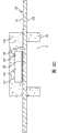
图1是现有微形芯片式麦克风结构的截面示意图。FIG. 1 is a schematic cross-sectional view of a conventional microchip microphone structure.

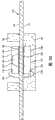
图2是依据本发明的第一具体实施例,一种微机电麦克风封装结构的截面示意图。FIG. 2 is a schematic cross-sectional view of a MEMS microphone package structure according to the first embodiment of the present invention.

图3A至图3D是依据本发明的第一具体实施例,该微机电麦克风封装过程中的截面示意图。3A to 3D are schematic cross-sectional views of the micro-electromechanical microphone during the packaging process according to the first embodiment of the present invention.

图4是依据本发明的第二具体实施例,另一种微机电麦克风封装结构的截面示意图。FIG. 4 is a schematic cross-sectional view of another MEMS microphone package structure according to the second specific embodiment of the present invention.

具体实施方式Detailed ways

请参阅图2,依据本发明的第一具体实施例揭示一种微机电麦克风封装结构100,该微机电麦克风封装结构100包含一承载器110、一特定应用芯片120、一封胶体130及一麦克风芯片140,该承载器110具有一第一表面111与一第二表面112,其中该承载器110可以是封装基板或导线架,在本实施例中,该承载器110为导线架,该特定应用芯片120设置于该承载器110的该第一表面111且电性连接该承载器110,该特定应用芯片120具有一主动面121、一背面122及至少一焊垫123,该特定应用芯片120的该背面122黏设于该承载器110的该第一表面111,该特定应用芯片120的该焊垫123形成于该特定应用芯片120的该主动面121,该微机电麦克风封装结构100另包含有至少一第一电连接组件150,该第一电连接组件150连接该承载器110与该特定应用芯片120的该焊垫123,其中该第一电连接组件150可以是焊球或焊线,在本实施例中,该第一电连接组件150为焊线。该封胶体130包含有一第一封胶体131及一第二封胶体132,该第一封胶体131形成于该承载器110的该第一表面111以密封该特定应用芯片120,该第二封胶体132形成于该承载器110的该第二表面112,在本实施例中,该第二封胶体132为环状,其可为「口」形或「O」形,该第二封胶体132与该承载器110形成有一容置空间A,该麦克风芯片140设置于该承载器110的该第二表面112且电性连接该承载器110,该麦克风芯片140位于该容置空间A中,该封胶体130的该第二封胶体132围绕该麦克风芯片140,该麦克风芯片140具有一主动面141、一背面142、一共振腔室143、一振膜1 44及至少一焊垫145,该焊垫145与该振膜144形成于该主动面141,该麦克风芯片140的该背面142黏设于该承载器110的该第二表面112,该微机电麦克风封装结构100另包含有至少一第二电连接组件160,该第二电连接组件160连接该麦克风芯片140的该焊垫145与该承载器110。该承载器110的若干个外引脚113裸露于该第一封胶体131与该第二封胶体132的外,其中该第一封胶体131与该第二封胶体132可以是移转注模成型材料(Transfer Molding Compound)、液态模封材料(Liquid Molding Compound)或底部充填胶,较佳地,该第一封胶体131与该第二封胶体132可为一体形成。此外,该微机电麦克风封装结构100另包含有一盖体170,该盖体170设置于该封胶体130的该第二封胶体132以罩盖及保护该麦克风芯片140与该第二电连接组件160,该盖体170的截面可为「一」或「ㄇ」形,该盖体170具有至少一音孔171以传导声波。由于该特定应用芯片120与该麦克风芯片140分别设置于该承载器110的该第一表面111及该第二表面112,因此,可缩小封装结构的尺寸,此外,由于该封胶体130的该第一封胶体131与该第二封胶体132分别形成于该承载器110的该第一表面111及该第二表面112,以密封该特定应用芯片120及围绕该麦克风芯片140,且该第一封胶体131与该第二封胶体132为一体形成,因此可增加封装结构强度及减少制程步骤。Please refer to FIG. 2 , according to the first embodiment of the present invention, a MEMSmicrophone package structure 100 is disclosed. The MEMSmicrophone package structure 100 includes acarrier 110, an application-specific chip 120, anencapsulant 130 and a microphone.Chip 140, thecarrier 110 has afirst surface 111 and asecond surface 112, wherein thecarrier 110 can be a packaging substrate or a lead frame, in this embodiment, thecarrier 110 is a lead frame, the specific application Thechip 120 is disposed on thefirst surface 111 of thecarrier 110 and is electrically connected to thecarrier 110. The application-specific chip 120 has anactive surface 121, aback surface 122 and at least onepad 123. The application-specific chip 120 Theback surface 122 is glued on thefirst surface 111 of thecarrier 110, thepad 123 of the application-specific chip 120 is formed on theactive surface 121 of the application-specific chip 120, and the MEMSmicrophone package structure 100 further includes At least one firstelectrical connection component 150, the firstelectrical connection component 150 connects thecarrier 110 and thepad 123 of thespecific application chip 120, wherein the firstelectrical connection component 150 can be a solder ball or a solder wire, in In this embodiment, the firstelectrical connection component 150 is a bonding wire. The sealingbody 130 includes afirst sealing body 131 and asecond sealing body 132, thefirst sealing body 131 is formed on thefirst surface 111 of thecarrier 110 to seal thespecific application chip 120, thesecond sealing body 132 is formed on thesecond surface 112 of thecarrier 110. In this embodiment, the second sealingbody 132 is ring-shaped, which can be "mouth" or "O". Thesecond sealing body 132 and Thecarrier 110 forms an accommodating space A, themicrophone chip 140 is disposed on thesecond surface 112 of thecarrier 110 and electrically connected to thecarrier 110, themicrophone chip 140 is located in the accommodating space A, the package Thesecond sealing body 132 of thecolloid 130 surrounds themicrophone chip 140, and themicrophone chip 140 has anactive surface 141, aback surface 142, aresonance chamber 143, adiaphragm 144 and at least onewelding pad 145, thewelding pad 145 and thediaphragm 144 are formed on theactive surface 141, theback surface 142 of themicrophone chip 140 is adhered to thesecond surface 112 of thecarrier 110, and the MEMSmicrophone package structure 100 further includes at least one second circuit Theconnection component 160 , the secondelectrical connection component 160 connects thebonding pad 145 of themicrophone chip 140 and thecarrier 110 . Severalouter pins 113 of thecarrier 110 are exposed outside thefirst molding body 131 and thesecond molding body 132, wherein thefirst molding body 131 and thesecond molding body 132 may be transfer injection molding materials (Transfer Molding Compound), Liquid Molding Compound (Liquid Molding Compound) or bottom filling compound, preferably, thefirst molding compound 131 and thesecond molding compound 132 can be integrally formed. In addition, the MEMSmicrophone packaging structure 100 further includes acover 170, thecover 170 is disposed on thesecond molding body 132 of themolding body 130 to cover and protect themicrophone chip 140 and the secondelectrical connection component 160. The cross-section of thecover 170 can be "-" or "ㄇ"-shaped, and thecover 170 has at least onesound hole 171 for conducting sound waves. Since the application-specific chip 120 and themicrophone chip 140 are disposed on thefirst surface 111 and thesecond surface 112 of thecarrier 110 respectively, the size of the packaging structure can be reduced. Anencapsulant 131 and asecond encapsulant 132 are respectively formed on thefirst surface 111 and thesecond surface 112 of thecarrier 110 to seal the application-specific chip 120 and surround themicrophone chip 140, and the first encapsulation Thecolloid 131 and thesecond colloid 132 are integrally formed, so the strength of the package structure can be increased and the process steps can be reduced.

请参阅图3A至图3D,其为第一实施例的微机电麦克风封装方法,首先,请参阅图3A,提供一承载器110,该承载器110具有一第一表面111与一第二表面112,在本实施例中,该承载器110为导线架。接着,请参阅图3B,设置一特定应用芯片120(ASIC,Application Specific IC)于该承载器110的该第一表面111,该特定应用芯片120的一背面122黏设于该承载器110的该第一表面111,形成至少一第一电连接组件150以连接该承载器110与该特定应用芯片120的至少一焊垫123,在本实施例中该第一电连接组件150为焊线。的后,请参阅图3C,形成一第一封胶体131于该承载器110的该第一表面111,该第一封胶体131密封该特定应用芯片120,以及形成一第二第二封胶体132于该承载器110的该第二表面112,该第二封胶体132与该承载器110形成一容置空间A,在本实施例中,该第二封胶体132为环状,其可为「口」形或「O」形,其中该第一封胶体131与该第二封胶体132是通过压模或点胶方法一体形成。接着,请参阅图3D,设置一麦克风芯片140于该容置空间A,该第二封胶体132系围绕该麦克风芯片140,该麦克风芯片140具有一主动面141、一背面142、一共振腔室143、一振膜144及至少一焊垫145,该振膜144及该焊垫145形成于该主动面141,该背面142黏设于该承载器110的该第二表面112,在此步骤中,另包含有形成至少一第二电连接组件160以连接该麦克风芯片140的该焊垫145与该承载器110。最后,如图2所示,设置一盖体170该第二封胶体132,该盖体170的截面可为「一」或「ㄇ」形,以保护该麦克风芯片140与该第二电连接组件160,该盖体170具有至少一音孔171以传导声波。Please refer to FIG. 3A to FIG. 3D , which are the MEMS microphone packaging method of the first embodiment. First, please refer to FIG. 3A , acarrier 110 is provided, and thecarrier 110 has afirst surface 111 and asecond surface 112 , in this embodiment, thecarrier 110 is a lead frame. Next, referring to FIG. 3B , a specific application chip 120 (ASIC, Application Specific IC) is set on thefirst surface 111 of thecarrier 110, and aback surface 122 of thespecific application chip 120 is bonded to thecarrier 110. Thefirst surface 111 forms at least one firstelectrical connection component 150 to connect thecarrier 110 and at least onepad 123 of the application-specific chip 120 , and in this embodiment, the firstelectrical connection component 150 is a bonding wire. Afterwards, referring to FIG. 3C, afirst encapsulant 131 is formed on thefirst surface 111 of thecarrier 110, the first encapsulant 131 seals the application-specific chip 120, and asecond second encapsulant 132 is formed. On thesecond surface 112 of thecarrier 110, thesecond sealing body 132 and thecarrier 110 form an accommodating space A. In this embodiment, thesecond sealing body 132 is ring-shaped, which can be " "O" shape or "O" shape, wherein thefirst sealant 131 and thesecond sealant 132 are integrally formed by molding or dispensing. Next, referring to FIG. 3D, amicrophone chip 140 is arranged in the accommodation space A, and the second sealingbody 132 surrounds themicrophone chip 140. Themicrophone chip 140 has anactive surface 141, aback surface 142, and a resonance chamber. 143. Adiaphragm 144 and at least onewelding pad 145, thediaphragm 144 and thewelding pad 145 are formed on theactive surface 141, theback surface 142 is adhered to thesecond surface 112 of thecarrier 110, in this step , further comprising forming at least one secondelectrical connection component 160 to connect thepad 145 of themicrophone chip 140 with thecarrier 110 . Finally, as shown in FIG. 2, acover body 170 and thesecond sealing body 132 are provided. The cross section of thecover body 170 can be "one" or "ㄇ" shape to protect themicrophone chip 140 and the second electrical connection component. 160, thecover 170 has at least onesound hole 171 for conducting sound waves.

此外,请再参阅图4,其为本发明的第二具体实施例,另一种微机电麦克风封装结构200,该微机电麦克风封装结构200包含一承载器210、一特定应用芯片220、一封胶体230及一麦克风芯片240。在本实施例中,该承载器210为封装基板,该承载器210具有一第一表面211与一第二表面212,该第一表面211形成有若干个第一连接垫213及若干个第二连接垫214,该第二表面212形成有至少一第三连接垫215,该特定应用芯片220设置于该承载器210的该第一表面211,且电性连接该承载器210,该特定应用芯片220具有一主动面221、一背面222及若干个焊垫223,该特定应用芯片220的该主动面221朝向该承载器210的该第一表面211,该微机电麦克风封装结构200另包含有若干个第一电连接组件250,在本实施例中该些第一电连接组件250为焊球,该些第一电连接组件250连接该承载器210的该些第一连接垫213与该特定应用芯片220的该些焊垫223,较佳地,该微机电麦克风封装结构200另包含有一被动组件260,该被动组件260设置于该承载器210的该第一表面211,该被动组件260是通过焊料设置于该承载器210的该些第二连接垫214上。该封胶体230包含有一第一封胶体231及一第二封胶体232,该第一封胶体231形成于该承载器210的该第一表面211以密封该特定应用芯片220及该被动组件260,该第二封胶体232形成于该承载器210的该第二表面212,且该第二封胶体232为环状,其可为「口」形或「O」形,该第二封胶体232与该承载器210形成一容置空间A’,该麦克风芯片240设置于该承载器210的该第二表面212且电性连接该承载器210,该麦克风芯片240位于该容置空间A’中,该麦克风芯片240具有一主动面241、一背面242、一共振腔室243、一振膜244及至少一焊垫245,该焊垫245与该振膜244形成于该主动面241,该麦克风芯片240的该背面242黏设于该承载器210的该第二表面212且该麦克风芯片240被该第二封胶体232所围绕,此外,在另一实施例中,该被动组件260可设置于该承载器210的该第二表面212,且该被动组件260被该第二封胶体232密封,该微机电麦克风封装结构200另包含有至少一第二电连接组件270,该第二电连接组件270连接该麦克风芯片240的该焊垫245与该承载器210的该第三连接垫215。其中该第一封胶体231与该第二封胶体232可以是移转注模成型材料(TransferMolding Compound)、液态模封材料(Liquid Molding Compound)或底部充填胶,较佳地,该第一封胶体231与该第二封胶体232可为一体形成。该微机电麦克风封装结构200另包含有一盖体280,该盖体280设置于该封胶体230的该第二封胶体232以保护该麦克风芯片240与该第二电连接组件270,该盖体270的截面可为「一」或「ㄇ」形,该盖体280具有至少一音孔281以传导声波。此外,该承载器210的该第一表面211另包含有若干个外接垫216以使该微机电麦克风封装结构200接合一外接组件(图未绘出)。该微机电麦克风封装结构200亦具有缩小封装结构的尺寸且增加封装结构强度的功效。In addition, please refer to FIG. 4 again, which is a second specific embodiment of the present invention, another MEMSmicrophone package structure 200, which includes acarrier 210, an application-specific chip 220, a package The colloid 230 and amicrophone chip 240 . In this embodiment, thecarrier 210 is a packaging substrate, thecarrier 210 has afirst surface 211 and asecond surface 212, thefirst surface 211 is formed with a plurality offirst connection pads 213 and a plurality of second Theconnection pad 214, thesecond surface 212 is formed with at least onethird connection pad 215, the application-specific chip 220 is disposed on thefirst surface 211 of thecarrier 210, and electrically connected to thecarrier 210, the application-specific chip 220 has anactive surface 221, aback surface 222 andseveral welding pads 223, theactive surface 221 of thespecific application chip 220 faces thefirst surface 211 of thecarrier 210, and the MEMSmicrophone package structure 200 also includes several A firstelectrical connection component 250, in this embodiment, these firstelectrical connection components 250 are solder balls, these firstelectrical connection components 250 connect thefirst connection pads 213 of thecarrier 210 with the specific application Thesolder pads 223 of thechip 220, preferably, the MEMSmicrophone package structure 200 further includes apassive component 260, thepassive component 260 is arranged on thefirst surface 211 of thecarrier 210, thepassive component 260 is passed Solder is disposed on thesecond connection pads 214 of thecarrier 210 . Thesealant 230 includes afirst sealant 231 and asecond sealant 232, thefirst sealant 231 is formed on thefirst surface 211 of thecarrier 210 to seal thespecific application chip 220 and thepassive component 260, Thesecond sealing body 232 is formed on thesecond surface 212 of thecarrier 210, and thesecond sealing body 232 is ring-shaped, which can be "mouth" shape or "O" shape, thesecond sealing body 232 and Thecarrier 210 forms an accommodating space A', themicrophone chip 240 is disposed on thesecond surface 212 of thecarrier 210 and electrically connected to thecarrier 210, themicrophone chip 240 is located in the accommodating space A', Themicrophone chip 240 has anactive surface 241, aback surface 242, aresonant chamber 243, adiaphragm 244 and at least onewelding pad 245, thewelding pad 245 and thediaphragm 244 are formed on theactive surface 241, the microphone chip Theback surface 242 of thecarrier 240 is adhered to thesecond surface 212 of thecarrier 210 and themicrophone chip 240 is surrounded by thesecond molding compound 232. In addition, in another embodiment, thepassive component 260 can be disposed on the Thesecond surface 212 of thecarrier 210, and thepassive component 260 is sealed by thesecond sealant 232, the MEMSmicrophone packaging structure 200 further includes at least one secondelectrical connection component 270, the secondelectrical connection component 270 Thebonding pad 245 of themicrophone chip 240 is connected to thethird connection pad 215 of thecarrier 210 . Wherein thefirst sealant 231 and thesecond sealant 232 can be transfer molding compound (TransferMolding Compound), liquid molding compound (Liquid Molding Compound) or bottom filling compound, preferably, thefirst sealant 231 It can be integrally formed with thesecond encapsulant 232 . The MEMSmicrophone packaging structure 200 further includes acover 280, thecover 280 is arranged on the second sealingbody 232 of the sealingbody 230 to protect themicrophone chip 240 and the secondelectrical connection component 270, thecover 270 The cross section of thecover body 280 can be in the shape of "-" or "ㄇ". Thecover body 280 has at least onesound hole 281 for conducting sound waves. In addition, thefirst surface 211 of thecarrier 210 further includes a plurality ofexternal pads 216 for connecting the MEMSmicrophone package structure 200 to an external component (not shown). The MEMSmicrophone packaging structure 200 also has the effect of reducing the size of the packaging structure and increasing the strength of the packaging structure.

Claims (12)

Translated fromChinese
1.一种微机电麦克风封装结构,其特征在于:其包含一承载器、一特定应用芯片、一封胶体、一麦克风芯片及一盖体;该承载器具有一第一表面与一第二表面;该特定应用芯片设置于该承载器的该第一表面且电性连接该承载器;封胶体包含有一第一封胶体及一第二封胶体,该第一封胶体形成于该承载器的该第一表面以密封该特定应用芯片,该第二封胶体形成于该承载器的该第二表面且与该承载器形成一容置空间;该麦克风芯片设置于该承载器的该第二表面且电性连接该承载器,该麦克风芯片位于该容置空间中;以及该盖体设置于该封胶体的该第二封胶体,该盖体具有至少一音孔。1. A micro-electromechanical microphone packaging structure, characterized in that: it comprises a carrier, an application-specific chip, encapsulating colloid, a microphone chip and a cover; the carrier has a first surface and a second surface; The application-specific chip is disposed on the first surface of the carrier and is electrically connected to the carrier; the encapsulant includes a first encapsulant and a second encapsulant, and the first encapsulant is formed on the second encapsulant of the carrier One surface is used to seal the specific application chip, the second sealing body is formed on the second surface of the carrier and forms an accommodating space with the carrier; the microphone chip is arranged on the second surface of the carrier and electrically The carrier is connected to the carrier, the microphone chip is located in the accommodating space; and the cover is disposed on the second molding of the molding, and the cover has at least one sound hole.2.如权利要求1所述的微机电麦克风封装结构,其特征在于:其另包含有至少一第一电连接组件及一第二电连接组件,该第一电连接组件为焊球或焊线,其电性连接该承载器与该特定应用芯片,该第二电连接组件电性连接该承载器与该麦克风芯片。2. The micro-electromechanical microphone packaging structure according to claim 1, characterized in that: it further comprises at least one first electrical connection component and a second electrical connection component, and the first electrical connection component is a solder ball or a bonding wire , which electrically connects the carrier and the specific application chip, and the second electrical connection component electrically connects the carrier and the microphone chip.3.如权利要求1所述的微机电麦克风封装结构,其特征在于:该第一封胶体与该第二封胶体为一体形成。3. The micro-electromechanical microphone packaging structure as claimed in claim 1, wherein the first encapsulant and the second encapsulant are integrally formed.4.如权利要求1所述的微机电麦克风封装结构,其特征在于:其另包含有一被动组件,该被动组件设置于该承载器的该第一表面,且被该第一封胶体密封。4. The MEMS microphone packaging structure according to claim 1, further comprising a passive component, the passive component is disposed on the first surface of the carrier and sealed by the first sealant.5.如权利要求1所述的微机电麦克风封装结构,其特征在于:其另包含有一被动组件,该被动组件设置于该承载器的该第二表面,且被该第二封胶体密封。5 . The MEMS microphone packaging structure according to claim 1 , further comprising a passive component, the passive component is disposed on the second surface of the carrier and sealed by the second sealant. 6 .6.如权利要求1所述的微机电麦克风封装结构,其特征在于:该第一封胶体与该第二封胶体是移转注模成型材料、液态模封材料或底部充填胶。6 . The micro-electromechanical microphone packaging structure as claimed in claim 1 , wherein the first encapsulant and the second encapsulant are transfer molding materials, liquid molding materials or underfill materials.7.一种微机电麦克风封装方法,其特征在于:其包含如下步骤:7. A MEMS microphone encapsulation method, characterized in that: it comprises the steps:提供一承载器,该承载器具有一第一表面与一第二表面;providing a carrier, the carrier has a first surface and a second surface;设置一特定应用芯片于该承载器的该第一表面,并且电性连接该特定应用芯片与该承载器;disposing an application-specific chip on the first surface of the carrier, and electrically connecting the application-specific chip to the carrier;形成一第一封胶体于该承载器的该第一表面,该第一封胶体密封该特定应用芯片;forming a first encapsulant on the first surface of the carrier, the first encapsulant seals the application-specific chip;形成一第二封胶体于该承载器的该第二表面,该第二封胶体与该承载器形成一容置空间;forming a second sealant on the second surface of the carrier, the second sealant and the carrier form an accommodating space;设置一麦克风芯片于该承载器的该第二表面,并且电性连接该麦克风芯片与该承载器,该麦克风芯片位于该容置空间中;以及disposing a microphone chip on the second surface of the carrier, and electrically connecting the microphone chip and the carrier, the microphone chip is located in the accommodating space; and设置一盖体于该第二封胶体,该盖体具有至少一音孔。A cover is arranged on the second sealing body, and the cover has at least one sound hole.8.如权利要求7所述的微机电麦克风封装方法,其特征在于:其另包含形成至少一第一电连接组件及一第二电连接组件,该第一电连接组件为焊球或焊线,其电性连接该承载器与该特定应用芯片,该第二电连接组件电性连接该承载器与该麦克风芯片。8. The MEMS microphone packaging method according to claim 7, further comprising forming at least one first electrical connection component and a second electrical connection component, the first electrical connection component being solder balls or bonding wires , which electrically connects the carrier and the specific application chip, and the second electrical connection component electrically connects the carrier and the microphone chip.9.如权利要求7所述的微机电麦克风封装方法,其特征在于:该第一封胶体与该第二封胶体为一体形成。9. The MEMS microphone packaging method as claimed in claim 7, wherein the first encapsulant and the second encapsulant are integrally formed.10.如权利要求7所述的微机电麦克风封装方法,其特征在于:其另包含有一被动组件,该被动组件设置于该承载器的该第一表面,且被该第一封胶体密封。10 . The MEMS microphone packaging method according to claim 7 , further comprising a passive component, the passive component is disposed on the first surface of the carrier and sealed by the first sealant. 11 .11.如权利要求7所述的微机电麦克风封装方法,其特征在于:其另包含有一被动组件,该被动组件设置于该承载器的该第二表面,且被该第二封胶体密封。11. The MEMS microphone packaging method according to claim 7, further comprising a passive component, the passive component is disposed on the second surface of the carrier and sealed by the second sealant.12.如权利要求7所述的微机电麦克风封装方法,其特征在于:该第一封胶体与该第二封胶体是以压模形成或点胶形成。12 . The MEMS microphone packaging method according to claim 7 , wherein the first encapsulant and the second encapsulant are formed by molding or dispensing. 13 .
CN2007101680731A2007-10-312007-10-31 MEMS Microphone Packaging Structure and MethodActiveCN101150889B (en)

Priority Applications (1)

Application NumberPriority DateFiling DateTitle
CN2007101680731ACN101150889B (en)2007-10-312007-10-31 MEMS Microphone Packaging Structure and Method

Applications Claiming Priority (1)

Application NumberPriority DateFiling DateTitle
CN2007101680731ACN101150889B (en)2007-10-312007-10-31 MEMS Microphone Packaging Structure and Method

Publications (2)

Publication NumberPublication Date
CN101150889A CN101150889A (en)2008-03-26
CN101150889Btrue CN101150889B (en)2011-05-25

Family

ID=39251145

Family Applications (1)

Application NumberTitlePriority DateFiling Date
CN2007101680731AActiveCN101150889B (en)2007-10-312007-10-31 MEMS Microphone Packaging Structure and Method

Country Status (1)

CountryLink
CN (1)CN101150889B (en)

Families Citing this family (5)

* Cited by examiner, † Cited by third party
Publication numberPriority datePublication dateAssigneeTitle
US8193596B2 (en)*2008-09-032012-06-05Solid State System Co., Ltd.Micro-electro-mechanical systems (MEMS) package
CN101734607B (en)*2008-11-202012-01-25纬拓科技股份有限公司Packaging structure of micro-electromechanical system
US10616690B2 (en)2016-08-222020-04-07Goertek Inc.Capacitive MEMS microphone and electronic apparatus
CN106744647A (en)*2016-12-202017-05-31苏州晶方半导体科技股份有限公司MEMS chip encapsulating structure and method for packing
CN112499577A (en)*2020-12-192021-03-16南京英锐创电子科技有限公司Packaging structure, preparation method thereof and electronic device

Citations (4)

* Cited by examiner, † Cited by third party
Publication numberPriority datePublication dateAssigneeTitle
CN1870836A (en)*2005-05-262006-11-29青岛歌尔电子有限公司Mini-packing silicon microphone
CN1917720A (en)*2005-08-202007-02-21宝星电子株式会社Silicon base capacitor microphone and its package method
WO2007054070A1 (en)*2005-11-102007-05-18Epcos AgMems package and method for the production thereof
CN1980854A (en)*2004-06-302007-06-13英特尔公司Module integrating MEMS and passive components

Patent Citations (4)

* Cited by examiner, † Cited by third party
Publication numberPriority datePublication dateAssigneeTitle
CN1980854A (en)*2004-06-302007-06-13英特尔公司Module integrating MEMS and passive components
CN1870836A (en)*2005-05-262006-11-29青岛歌尔电子有限公司Mini-packing silicon microphone
CN1917720A (en)*2005-08-202007-02-21宝星电子株式会社Silicon base capacitor microphone and its package method
WO2007054070A1 (en)*2005-11-102007-05-18Epcos AgMems package and method for the production thereof

Also Published As

Publication numberPublication date
CN101150889A (en)2008-03-26

Similar Documents

PublicationPublication DateTitle
US7829961B2 (en)MEMS microphone package and method thereof
TWI333264B (en)Packaging structure and method of mems microphone
CN101620022B (en) Pressure sensing element package and manufacturing method thereof
JP5763682B2 (en) Miniaturized electrical device including MEMS and ASIC and method for manufacturing the same
CN102201414B (en)Semiconductor memory device and manufacturing same
CN101221946B (en)Semiconductor package and method for manufacturing system-in-package module
JP4277079B2 (en) Semiconductor acceleration sensor device and manufacturing method thereof
US8104356B2 (en)Pressure sensing device package and manufacturing method thereof
CN107742630B (en) Image sensor package structure
CN104030233B (en)Top port MEMS cavity encapsulates
CN100587430C (en) A substrate-based silicon piezoresistive pressure sensor packaging structure
CN102110678B (en) Semiconductor package and manufacturing method thereof
CN102315225A (en)Semiconductor storage and manufacturing approach thereof
TW201229479A (en)Pressure sensor and method of assembling same
CN103489833A (en)Chip-packaging module for a chip and a method for forming a chip-packaging module
CN101150889B (en) MEMS Microphone Packaging Structure and Method
CN101337652A (en)Packaging of sensor element contact surfaces and packaging method thereof
CN101150886B (en) Packaging Structure and Packaging Method of MEMS Microphone
CN101150888B (en) MEMS Microphone Packaging Structure and Packaging Method
CN111217318B (en) Sensors and packaging components
CN101734607A (en)Packaging structure of micro-electromechanical system
CN101155437B (en) Back-mounted microphone module structure, microphone chip assembly and manufacturing method thereof
KR20160017412A (en)Stack type semiconductor package structure by use of cavity substrate and method thereof
CN103762200A (en)Chip packaging part and packaging method of chip packaging part
CN1835227B (en)Semiconductor package

Legal Events

DateCodeTitleDescription
C06Publication
PB01Publication
C10Entry into substantive examination
SE01Entry into force of request for substantive examination
C14Grant of patent or utility model
GR01Patent grant

[8]ページ先頭

©2009-2025 Movatter.jp