CN101144929B - Double-visual image display panel structure and manufacturing method thereof - Google Patents
Double-visual image display panel structure and manufacturing method thereofDownload PDFInfo
- Publication number
- CN101144929B CN101144929BCN2007101814280ACN200710181428ACN101144929BCN 101144929 BCN101144929 BCN 101144929BCN 2007101814280 ACN2007101814280 ACN 2007101814280ACN 200710181428 ACN200710181428 ACN 200710181428ACN 101144929 BCN101144929 BCN 101144929B
- Authority
- CN
- China
- Prior art keywords
- display panel
- layer
- patterned shielding
- substrate
- material layer
- Prior art date
- Legal status (The legal status is an assumption and is not a legal conclusion. Google has not performed a legal analysis and makes no representation as to the accuracy of the status listed.)
- Active
Links
- 238000004519manufacturing processMethods0.000titleclaimsabstractdescription36
- 239000000758substrateSubstances0.000claimsabstractdescription90
- 239000007788liquidSubstances0.000claimsabstractdescription18
- 238000000034methodMethods0.000claimsdescription42
- 239000012780transparent materialSubstances0.000claimsdescription41
- 239000011521glassSubstances0.000claimsdescription34
- 230000000694effectsEffects0.000claimsdescription30
- 239000004973liquid crystal related substanceSubstances0.000claimsdescription14
- 239000000463materialSubstances0.000claimsdescription14
- 208000003164DiplopiaDiseases0.000claimsdescription10
- 208000029444double visionDiseases0.000claimsdescription10
- 239000011347resinSubstances0.000claimsdescription9
- 229920005989resinPolymers0.000claimsdescription9
- 239000011368organic materialSubstances0.000claimsdescription8
- 239000002861polymer materialSubstances0.000claimsdescription5
- 239000011248coating agentSubstances0.000claimsdescription3
- 238000000576coating methodMethods0.000claimsdescription3
- 210000004276hyalinAnatomy0.000claims3
- 239000000284extractSubstances0.000claims1
- 238000002347injectionMethods0.000claims1
- 239000007924injectionSubstances0.000claims1
- 238000010422paintingMethods0.000claims1
- 239000000126substanceSubstances0.000abstractdescription12
- 238000012797qualificationMethods0.000abstractdescription2
- 230000000873masking effectEffects0.000description32
- 238000010586diagramMethods0.000description5
- 238000003384imaging methodMethods0.000description5
- 238000004528spin coatingMethods0.000description4
- 230000009977dual effectEffects0.000description2
- 238000002834transmittanceMethods0.000description2
- 238000000149argon plasma sinteringMethods0.000description1
- 230000000903blocking effectEffects0.000description1
- 230000007547defectEffects0.000description1
- 239000011159matrix materialSubstances0.000description1
- 230000003287optical effectEffects0.000description1
- 238000005498polishingMethods0.000description1
- 230000000717retained effectEffects0.000description1
- 238000007650screen-printingMethods0.000description1
- 239000002904solventSubstances0.000description1
- 239000010409thin filmSubstances0.000description1
Images


Landscapes
- Devices For Indicating Variable Information By Combining Individual Elements (AREA)
Abstract
Translated fromChinese
Description
Translated fromChinese技术领域technical field
本发明涉及一种液晶显示面板结构及其制造方法,更详细地说,涉及一种双视像显示面板结构及其制造方法。The present invention relates to a structure of a liquid crystal display panel and a manufacturing method thereof, more specifically, to a structure of a dual-image display panel and a manufacturing method thereof.
背景技术Background technique
双视像显示器(dual view display)的主要功能是显示不同角度的二维影像,亦即使用者可以从不同的角度看到不同的影像,其主要可应用在车用显示器上。举例来说,通过双视像显示器,可使车内不同座位的乘客通过同一部显示器分别看到不同的影像,这样不需要对每位乘客提供个别的显示器,可节省显示器设置的成本以及减少车内空间的占用。The main function of a dual view display is to display two-dimensional images from different angles, that is, users can see different images from different angles, and it can be mainly applied to vehicle displays. For example, through the dual-view display, passengers in different seats in the car can see different images through the same display, so that there is no need to provide individual displays for each passenger, which can save the cost of display settings and reduce the cost of the car. occupancy of internal space.
双视像显示器的成像原理主要是利用一图案化遮蔽层的遮蔽作用使左右两边观看像素层上的同一像素时,某一边将由于图案化遮蔽层的阻挡而无法看到该像素,因此左右两边可各自看到不同的影像,以达到双视像的效果。The imaging principle of the dual-view display is mainly to use the shielding effect of a patterned shielding layer to make the left and right sides watch the same pixel on the pixel layer, and one side will not be able to see the pixel due to the blocking of the patterned shielding layer, so the left and right sides Different images can be seen separately to achieve the effect of double vision.
请参阅图1,其为一已有的双视像显示面板结构10的成像示意图,此双视像显示面板结构包括一第二基板11、一液晶层12、一像素层13、一第一基板14、一图案化遮蔽层15以及一透明基板16,其中图案化遮蔽层15包括不透明的遮蔽层图案151、152、153及154。此结构与非双视像液晶面板结构不同之处主要是在于,双视像显示面板结构通过图案化遮蔽层15的作用来产生双视像的显示效果。Please refer to FIG. 1 , which is an imaging schematic diagram of an existing dual-view
以下通过图1说明双视像显示效果的原理。当使用者分别从左视角及右视角观看像素层13的左影像的同一像素时,右视角所看到的像素所发出的光线将被遮蔽层图案152所阻挡,而左视角所看到的像素所发出的光线则未受到任何遮蔽层图案阻挡而直接穿过图案化遮蔽层15。同理,右影像所发出的光线,左视角被遮蔽层图案152所阻挡,而右视角则可看到像素所发出的光线。这样左右视角看到的像素将有所不同,从而产生双视像的效果。The principle of the dual-view display effect will be described below with reference to FIG. 1 . When the user views the same pixel of the left image of the
已有的双视像显示面板的制造方法中,多种因素可能影响到工艺过程的合格率,例如所需的玻璃层数、遮蔽层厚度的均匀程度、以及基板间存在的空气间隙程度等,以上因素均可能造成左右影像重叠,而使得影像可视角度较小。因此,如何改善双视像显示面板的制造方法,以简化工艺并提升制造合格率,并增大影像的可视角度,这是一业界亟待解决的问题。In the existing manufacturing methods of dual-view display panels, various factors may affect the qualification rate of the process, such as the number of glass layers required, the uniformity of the thickness of the shielding layer, and the degree of air gaps between the substrates, etc., All of the above factors may cause the left and right images to overlap, resulting in a smaller viewing angle of the image. Therefore, how to improve the manufacturing method of the dual-view display panel, so as to simplify the process, improve the manufacturing yield, and increase the viewing angle of the image, is an urgent problem to be solved in the industry.
发明内容Contents of the invention
本发明的一目的在于提供一种制造一双视像显示面板(dual-view displaypanel)结构的方法。通过此方法,可减少显示面板所需的玻璃层数,进而提升显示面板的透光率,并增大影像的可视角度。An object of the present invention is to provide a method for manufacturing a dual-view display panel structure. Through this method, the number of glass layers required by the display panel can be reduced, thereby increasing the light transmittance of the display panel and increasing the viewing angle of images.
为达到上述目的,此方法包括下列步骤:提供一显示面板,该显示面板至少包括一玻璃基板;将该玻璃基板薄化至一预定厚度,其中,该预定厚度与该图案化遮蔽层上的不透明图案的宽度相关;以及在该玻璃基板上形成一图案化遮蔽层,用于产生双视像效果。To achieve the above object, the method includes the following steps: providing a display panel, the display panel at least includes a glass substrate; thinning the glass substrate to a predetermined thickness, wherein the predetermined thickness is the same as the opaque layer on the patterned masking layer The width of the patterns is related; and a patterned shielding layer is formed on the glass substrate for producing double-image effects.
本发明的另一目的在于提供一种制造双视像显示面板结构的方法。通过此方法,可改善透明材料层的厚度不均匀造成的面板间的间隙过大,导致可视角度降低的问题,以提高制造合格率。Another object of the present invention is to provide a method for manufacturing a dual-view display panel structure. Through this method, the problem of reduced viewing angle caused by the excessively large gap between the panels caused by the uneven thickness of the transparent material layer can be improved, so as to improve the manufacturing yield.
为达到上述目的,此方法包括下列步骤:在一第一基板上形成一图案化遮蔽层,用于产生双视像效果;在该图案化遮蔽层上形成一透明材料层,该透明材料层用以搭配该图案化遮蔽层产生双视像效果;在该透明材料层上形成一平坦化层,该平坦化层用以控制该透明材料层的厚度的均匀度;在该平坦化层上形成一像素层;以及将一第二基板与该第一基板组装成一显示面板。In order to achieve the above object, the method includes the following steps: forming a patterned shielding layer on a first substrate for producing a double-view effect; forming a transparent material layer on the patterned shielding layer, and using the transparent material layer The patterned masking layer is used to produce a dual-image effect; a planarization layer is formed on the transparent material layer, and the planarization layer is used to control the uniformity of the thickness of the transparent material layer; a planarization layer is formed on the planarization layer a pixel layer; and assembling a second substrate and the first substrate into a display panel.
本发明的又一目的在于提供一种双视像显示面板结构。通过在显示面板的透明材料层上涂布一层平坦化层,可使整个厚度较为均匀,以减少间隙的产生,这样可增大可视角度,以提高显示面板的制造合格率。Another object of the present invention is to provide a dual-view display panel structure. By coating a planarizing layer on the transparent material layer of the display panel, the entire thickness can be made relatively uniform to reduce the generation of gaps, which can increase the viewing angle and improve the manufacturing yield of the display panel.
为达到上述目的,此结构包括一第一基板;一图案化遮蔽层,形成于该第一基板上,用于产生双视像效果;一透明材料层,形成于该图案化遮蔽层上,该透明材料层用以搭配该图案化遮蔽层产生双视像效果;一平坦化层,形成于该透明材料层上,该平坦化层用以控制该透明材料层的厚度的均匀度;一像素层,形成于该平坦化层上;以及一第二基板,与该第一基板组装形成一显示面板。In order to achieve the above purpose, the structure includes a first substrate; a patterned shielding layer formed on the first substrate for producing a double-view effect; a transparent material layer formed on the patterned shielding layer, the The transparent material layer is used to cooperate with the patterned masking layer to produce a double-image effect; a planarization layer is formed on the transparent material layer, and the planarization layer is used to control the uniformity of the thickness of the transparent material layer; a pixel layer , formed on the planarization layer; and a second substrate, assembled with the first substrate to form a display panel.
本发明的再一目的在于提供一种制造双视像显示面板结构的方法。通过此方法,显示面板当中的空气间隙可被一透明液态物质所填满,这样可减少产生不正确影像的情况,并提高显示面板的合格率。Another object of the present invention is to provide a method for manufacturing a dual-view display panel structure. Through this method, the air gap in the display panel can be filled with a transparent liquid substance, which can reduce the occurrence of incorrect images and improve the yield of the display panel.
为达到上述目的,此方法包括下列步骤:提供一显示面板;在一第一基板上形成一图案化遮蔽层,用于产生双视像效果;将具有该图案化遮蔽层的该第一基板贴附于该显示面板上,其中该显示面板与该图案化遮蔽层之间具有一间隙;以及在该间隙中注入一液态透明物质,以形成一透明层。In order to achieve the above object, the method includes the following steps: providing a display panel; forming a patterned shielding layer on a first substrate to produce a double-view effect; pasting the first substrate with the patterned shielding layer Attached to the display panel, wherein there is a gap between the display panel and the patterned shielding layer; and injecting a liquid transparent substance into the gap to form a transparent layer.
本发明的再一目的在于提供一种双视像显示面板结构。通过在显示面板的空气间隙中注入一透明液态物质,可改善原本容易产生不正确影像的缺点,进而增大显示面板的可视角度。Another object of the present invention is to provide a dual-view display panel structure. By injecting a transparent liquid substance into the air gap of the display panel, the original defect of easily generating incorrect images can be improved, thereby increasing the viewing angle of the display panel.
为达到上述目的,此结构包括一显示面板;一透明基板;一图案化遮蔽层,形成于该透明基板上,用于产生双视像效果;以及一透明层,形成于该图案化遮蔽层与该显示面板间的一间隙中,且该透明层的材质为液态透明物质。To achieve the above purpose, the structure includes a display panel; a transparent substrate; a patterned shielding layer formed on the transparent substrate for producing a double-view effect; and a transparent layer formed on the patterned shielding layer and the In a gap between the display panels, and the material of the transparent layer is a liquid transparent substance.
综上所述,本发明提供一种双视像显示面板结构及其制造方法。通过本发明,可改善已有的双视像显示面板的结构,以避免产生不正确影像,可增大显示面板的可视角度,并提高制造的合格率。To sum up, the present invention provides a dual-view display panel structure and a manufacturing method thereof. Through the present invention, the structure of the existing dual-view display panel can be improved to avoid incorrect images, the viewing angle of the display panel can be increased, and the qualified rate of manufacture can be improved.
在参阅附图及随后描述的实施方式后,本领域技术人员就可了解本发明的其它目的,以及本发明的技术手段及实施方式。After referring to the accompanying drawings and the implementations described later, those skilled in the art can understand other objectives of the present invention, as well as the technical means and implementations of the present invention.
附图说明Description of drawings
图1是已有双视像显示面板成像的结构示意图;Fig. 1 is a structural schematic diagram of imaging of an existing dual-vision display panel;
图2A是本发明第一实施例的结构示意图;Fig. 2A is a schematic structural diagram of the first embodiment of the present invention;
图2B是本发明第一实施例的方法流程图;Fig. 2B is a method flow chart of the first embodiment of the present invention;
图3A是本发明第二实施例的结构示意图;3A is a schematic structural diagram of a second embodiment of the present invention;
图3B是本发明第二实施例的方法流程图;Fig. 3B is a flow chart of the method of the second embodiment of the present invention;
图4A是本发明第三实施例的结构示意图;以及FIG. 4A is a schematic structural diagram of a third embodiment of the present invention; and
图4B是本发明第三实施例的方法流程图。Fig. 4B is a flow chart of the method of the third embodiment of the present invention.
其中,附图标记说明如下:Wherein, the reference signs are explained as follows:
10已有双视像液晶面板结构 11第二基板10 Existing dual-view liquid
12液晶层 13像素层12
14第一基板 15图案化遮蔽层14 The
151、152、153、154遮蔽层图案 16透明基板151, 152, 153, 154
20双视像液晶面板结构 21显示面板20 dual-view
211玻璃基板 212数组基板211
23图案化遮蔽层 24平坦化层23 patterned
25偏光层 30双视像液晶面板结构25 polarizing
31第一基板 32图案化遮蔽层31 The
33透明材料层 34平坦化层33
35像素层 36第二基板35
40双视像液晶面板结构 41透明基板40 dual-view liquid
42图案化遮蔽层 43透明层42 patterned
44显示面板44 display panel
具体实施方式Detailed ways
以下将通过实施例来解释本发明内容。本发明涉及一种双视像显示面板结构及其制造方法。然而,本发明的实施例并非用以限制本发明必须在如实施例所述的任何特定的环境、应用或特殊方式情况下才能实施。因此,关于实施例的说明仅用于阐释本发明的目的,而非用以限制本发明。需要说明的是,以下实施例及附图中,与本发明无关的元件已省略而未示出。The content of the present invention will be explained below through examples. The invention relates to a dual-image display panel structure and a manufacturing method thereof. However, the embodiments of the present invention are not intended to limit the present invention to be implemented in any specific environment, application or special manner as described in the embodiments. Therefore, the descriptions about the embodiments are only for the purpose of explaining the present invention rather than limiting the present invention. It should be noted that, in the following embodiments and drawings, elements irrelevant to the present invention have been omitted and not shown.
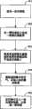
图2A描绘本发明的第一实施例,其是一种双视像显示面板结构20。双视像显示面板结构20包括一显示面板21、一图案化遮蔽层23、、一平坦化层24以及一偏光层25。其中显示面板21至少包括一玻璃基板211,例如是彩色滤光基板,此外显示面板还包括一阵列基板212,另外还可包括其它已有的显示元件,如玻璃基板211上的像素层(图未示),以及阵列基板212与玻璃基板211之间的液晶层(图未示)等。玻璃基板211用以形成图案化遮蔽层23的表面,图案化遮蔽层23用以产生双视像效果,平坦化层24则是在图案化遮蔽层23之上形成一有机材料层以形成一较为平坦的表面,以减少组合时空气间隙的产生。以下将详细说明双视像显示面板结构20的制造方法。FIG. 2A depicts a first embodiment of the present invention, which is a dual-view
请参阅图2B,其是制造双视像显示面板结构20的流程图。首先执行步骤201,提供一显示面板21,该显示面板21至少包括一玻璃基板211。接着执行步骤202,将该玻璃基板211薄化至一预定厚度。具体而言,此步骤是将玻璃基板211的厚度薄化至实质上为30至200微米,如本实施例中为50微米。需注意的是,玻璃基板211的厚度与图案化遮蔽层23上不透明图案的宽度相关,也就是当要通过图案化遮蔽层23产生双视像效果时,玻璃基板211的厚度与不透明图案的宽度须具备一对应关系,否则将影响双视像的成像效果。薄化玻璃基板211的方法例如可使用化学机械研磨法(CMP),可以达到完全均匀薄化的效果。Please refer to FIG. 2B , which is a flowchart of manufacturing the dual-view
薄化玻璃基板211后,执行步骤203,在该玻璃基板211上形成一图案化遮蔽层。此步骤可先在该玻璃基板211上形成一遮蔽层,再图案化该遮蔽层,以形成一图案化遮蔽层23,或者直接在该玻璃基板211上形成一图案化遮蔽层23。通过这些不透明遮蔽图案的遮蔽效果,可产生双视像的显示效果。After the
以下进一步说明遮蔽层图案的产生方式。第一种方式为使用网版印刷在该玻璃基板211上形成该图案化遮蔽层23。具体而言,此种方式将不透明黑色树脂印到薄化后的玻璃基板211的表面上以直接形成遮蔽层图案,再经过烘烤工艺过程,将树脂内的溶剂完全挥发,并让不透明黑色树脂反应完全稳定,这样就完成遮蔽图案的制作。The generation method of the masking layer pattern is further described below. The first method is to form the patterned
另一种方式则是在该玻璃基板211上形成一不透光的黑色树脂。具体而言,此种方式将不透明的黑色树脂涂布在薄化后的玻璃基板211的表面,经过曝光与显影过程,将不透明区的黑色树脂保留,将透明区黑色树脂曝掉,最后再经过高温烘烤工艺,使黑色树脂反应完全,这样就可产生遮蔽图案。Another way is to form an opaque black resin on the
由于遮蔽图案的缘故,造成图案化遮蔽层23的表面产生些许不平坦的情况。若直接将图案化遮蔽层23与显示面板组合,将容易产生空气间隙而影响到双视像效果。因此,在形成图案化遮蔽层23后可执行步骤204,在该图案化遮蔽层23上形成一平坦化层24,也就是在该图案化遮蔽层23上形成一有机材料层,这样当组合显示面板时就可减少空气间隙的产生。此外,最后可执行步骤205,在该图案化遮蔽层上23形成一偏光层25。Due to the masking pattern, the surface of the patterned
本实施例的制造一双视像显示面板结构20的方法,是直接在玻璃基板211上形成图案化遮蔽层23,和已有方法比较起来,可减少所需玻璃层数以提高透光率,这样可使双视像的成像效果更好。此外,此方法还可避免已有技术中两片玻璃组合时容易产生误差的缺点。The method for manufacturing a dual-video
本发明的第二实施例如图3A所示,其是一种双视像显示面板结构30。双视像显示面板结构30包括一第一基板31、一图案化遮蔽层32、一透明材料层33、一平坦化层34、一像素层35及一第二基板36。The second embodiment of the present invention is shown in FIG. 3A , which is a dual-view
其中,第一基板31可为彩色滤光基板,图案化遮蔽层32形成于第一基板31上,用以产生双视像的效果。透明材料层33形成于该图案化遮蔽层32上,此透明材料层33的材质为透明高分子材料,并用以搭配图案化遮蔽层32以产生双视像效果。平坦化层34形成于该透明材料层33上,用以控制透明材料层33的厚度的均匀度,其材质是有机材料。像素层35形成于该平坦化层34上,像素层35例如是彩色滤光层,可由彩色滤光层中的黑色矩阵(Black matrix)定义出像素的位置。第二基板36包括薄膜晶体管阵列的阵列层,其与第一基板31组装形成显示面板,组装时像素层35与阵列层向内,并在第一基板31与第二基板36之间注入液晶层(图未示),此为本领域技术人员所熟知的工艺,因此不再赘述。Wherein, the
在此双视像显示面板结构30中,由于透明材料层33以旋转涂布方式在该图案化遮蔽层32上形成透明高分子材料层,而此透明材料层33的厚度范围与第一实施例所述的30至200微米相同,如以本实施例中透明材料层33的厚度50微米为例,并以涂布均匀度为3%计算,其厚度差异将可达到1.5微米,这样将无法达到液晶面板间隙值均匀性的0.3微米的要求,从而使得合格率降低。由于透明材料层33的均匀度过低会导致光散射的增加,进而降低影像的清晰度,因此在透明材料层33上形成厚度约4微米的平坦化层34,即可将整体厚度均匀度控制在0.3微米以下。In this dual-view
以下将说明制造双视像显示面板结构30的流程。请参阅图3B,首先执行步骤301,在一第一基板31上形成一图案化遮蔽层32,接着执行步骤302,在该图案化遮蔽层32上形成一透明材料层33。具体而言,在该图案化遮蔽层32上形成该透明材料层33的步骤是以旋转涂布方式在该图案化遮蔽层32上形成一高分子材料层。The process of manufacturing the dual-view
然后执行步骤303,在该透明材料层33上形成一平坦化层34。具体而言,在该透明材料层33上形成该平坦化层34的步骤是以旋转涂布方式在该透明材料层33上形成一有机材料层,且较佳地是使用低黏度、高坦(涂)覆性的有机材料进行涂布,以作为平坦化层34。最后执行步骤304,在该平坦化层34上形成一像素层35,以及执行步骤305,将一第二基板36与该第一基板31组装成一显示面板。Then step 303 is executed to form a
本实施例的双视像显示面板结构30及其制造方法是以旋转涂布方式形成一厚度约50微米的透明材料层33后,再形成一平坦化层34,以避免由于透明材料层33的工艺容差控制不当而产生厚度不均匀的误差,这样可改善双视像液晶面板的间隙不均匀造成的合格率损失。In the dual-view
本发明的第三实施例如图4A所示,其是一种双视像显示面板结构40。双视像显示面板结构40包括一透明基板41、一图案化遮蔽层42、一透明层43、及一显示面板44。其中图案化遮蔽层42形成于该透明基板41上,用以产生双视像的显示效果。在实际方式中,显示面板44可包括一第一基板441、形成于该第一基板441上的一像素层442、一液晶层443及一第二基板444,其中液晶层443位于该像素层442与该第二基板444之间。透明层43形成于图案化遮蔽层42与显示面板44之间的一间隙中,且该透明层43的材质为液态透明物质。The third embodiment of the present invention is shown in FIG. 4A , which is a dual-view
在本实施例中,将具有该图案化遮蔽层42的该透明基板41贴附于该显示面板44,以制造双视像显示面板结构40。但在实际工艺过程当中,显示面板44和图案化遮蔽层42之间往往存在空气间隙,而此空气间隙将大幅度地降低双视像显示器的可视角度。因此,在显示面板44和图案化遮蔽层42之间隙注入一折射率大于空气的液态透明物质,如光学油等,以形成一透明层43,这样可使空气间隙完全被填满,以避免空气间隙所造成的影响。In this embodiment, the
以下将说明制造双视像显示面板结构40的流程。请参照图4B,其是制造双视像液晶显示面板结构40的流程图。首先执行步骤401,提供一显示面板44,接着执行步骤402,在一透明基板41上形成一图案化遮蔽层42;接着执行步骤403,将具有该图案化遮蔽层42的该透明基板41贴附于该显示面板44,此时该显示面板44与该图案化遮蔽层42之间将会具有一间隙。The process of manufacturing the dual-view
在该间隙尚未注入液态透明物质之前,可先执行步骤404,抽取该间隙中的空气以缩小该间隙的距离,这样可使透明基板41与显示面板44组合时的准确度更高。最后再执行步骤405,在该间隙中注入一液态透明物质以形成一透明层43。此液态透明物质如前所述,此处不再赘述。Before the liquid transparent substance is injected into the gap, step 404 can be performed to extract the air in the gap to reduce the distance of the gap, so that the accuracy of combining the
本实施例的双视像显示面板结构40及其制造方法是在显示面板44与图案化遮蔽层42之间的空气间隙中注入一液态透明物质,以避免空气间隙造成的影响。一方面可提高双视像显示器的可视角度,另一方面还可提高制造合格率。In the dual-view
综上所述,本发明提供一种双视像显示面板结构及其制造方法。通过本发明所提出新的结构与工艺方法,一方面使双视像显示器有较大的可视角度,另一方面还可提高合格率,这样可减少已有技术中可视角度较小及合格率较差等缺点。To sum up, the present invention provides a dual-view display panel structure and a manufacturing method thereof. Through the new structure and process method proposed by the present invention, on the one hand, the dual-vision display has a larger viewing angle, and on the other hand, the pass rate can be improved, which can reduce the small viewing angle and the pass rate in the prior art. Disadvantages such as poor rate.
上述的实施例仅用来举例说明本发明的实施方式以及阐释本发明的技术特征,并非用来限制本发明的范围。本领域技术人员可轻易完成的改变或等同替换均属于本发明所要求保护的范围,本发明的保护范围应以权利要求书为准。The above-mentioned embodiments are only used to illustrate the implementation of the present invention and explain the technical features of the present invention, and are not intended to limit the scope of the present invention. Changes or equivalent replacements that can be easily accomplished by those skilled in the art all belong to the protection scope of the present invention, and the protection scope of the present invention should be determined by the claims.
Claims (22)
Priority Applications (1)
| Application Number | Priority Date | Filing Date | Title |
|---|---|---|---|
| CN2007101814280ACN101144929B (en) | 2007-10-25 | 2007-10-25 | Double-visual image display panel structure and manufacturing method thereof |
Applications Claiming Priority (1)
| Application Number | Priority Date | Filing Date | Title |
|---|---|---|---|
| CN2007101814280ACN101144929B (en) | 2007-10-25 | 2007-10-25 | Double-visual image display panel structure and manufacturing method thereof |
Publications (2)
| Publication Number | Publication Date |
|---|---|
| CN101144929A CN101144929A (en) | 2008-03-19 |
| CN101144929Btrue CN101144929B (en) | 2010-06-09 |
Family
ID=39207526
Family Applications (1)
| Application Number | Title | Priority Date | Filing Date |
|---|---|---|---|
| CN2007101814280AActiveCN101144929B (en) | 2007-10-25 | 2007-10-25 | Double-visual image display panel structure and manufacturing method thereof |
Country Status (1)
| Country | Link |
|---|---|
| CN (1) | CN101144929B (en) |
Families Citing this family (3)
| Publication number | Priority date | Publication date | Assignee | Title |
|---|---|---|---|---|
| JP2011099880A (en)* | 2009-11-03 | 2011-05-19 | Sony Corp | Method for manufacturing liquid crystal display device |
| CN101907796B (en)* | 2010-03-22 | 2012-02-22 | 福建华映显示科技有限公司 | Method for manufacturing double-visual area liquid crystal display |
| CN102566146B (en)* | 2010-12-23 | 2015-01-21 | 京东方科技集团股份有限公司 | Liquid crystal panel, liquid crystal panel production method and liquid crystal display |
Citations (6)
| Publication number | Priority date | Publication date | Assignee | Title |
|---|---|---|---|---|
| US5717522A (en)* | 1994-07-27 | 1998-02-10 | Fuji Photo Optical Co., Ltd. | Polarizing films used for optical systems and three-dimensional image displaying apparatuses using the polarizing films |
| US6215590B1 (en)* | 1998-02-09 | 2001-04-10 | Kabushiki Kaisha Toshiba | Stereoscopic image display apparatus |
| US20020030888A1 (en)* | 1996-10-16 | 2002-03-14 | Paul Kleinberger | Systems for three-dimensional viewing and projection |
| CN1514271A (en)* | 2002-12-07 | 2004-07-21 | ������������ʽ���� | multi-view display |
| CN1834729A (en)* | 2005-03-17 | 2006-09-20 | 三洋爱普生映像元器件有限公司 | Image display apparatus |
| US20060279567A1 (en)* | 2003-08-26 | 2006-12-14 | Seereal Technologies Gmbh | Autostereoscopic multi-user display |
- 2007
- 2007-10-25CNCN2007101814280Apatent/CN101144929B/enactiveActive
Patent Citations (6)
| Publication number | Priority date | Publication date | Assignee | Title |
|---|---|---|---|---|
| US5717522A (en)* | 1994-07-27 | 1998-02-10 | Fuji Photo Optical Co., Ltd. | Polarizing films used for optical systems and three-dimensional image displaying apparatuses using the polarizing films |
| US20020030888A1 (en)* | 1996-10-16 | 2002-03-14 | Paul Kleinberger | Systems for three-dimensional viewing and projection |
| US6215590B1 (en)* | 1998-02-09 | 2001-04-10 | Kabushiki Kaisha Toshiba | Stereoscopic image display apparatus |
| CN1514271A (en)* | 2002-12-07 | 2004-07-21 | ������������ʽ���� | multi-view display |
| US20060279567A1 (en)* | 2003-08-26 | 2006-12-14 | Seereal Technologies Gmbh | Autostereoscopic multi-user display |
| CN1834729A (en)* | 2005-03-17 | 2006-09-20 | 三洋爱普生映像元器件有限公司 | Image display apparatus |
Also Published As
| Publication number | Publication date |
|---|---|
| CN101144929A (en) | 2008-03-19 |
Similar Documents
| Publication | Publication Date | Title |
|---|---|---|
| KR100680672B1 (en) | Parallax barrier element, method of manufacturing the same, and display device | |
| US20100182686A1 (en) | Image display device, electronic device, and parallax barrier element | |
| US20150285968A1 (en) | Color filter substrate, preparing method thereof, and display device | |
| CN101297236A (en) | Display device, method for manufacturing display device, substrate, and color filter substrate | |
| US10254581B2 (en) | Fabricating method of color filter substrate, color filter substrate and display device | |
| WO2006098475A1 (en) | Panel and method for manufacturing same | |
| US20150124200A1 (en) | Color filter substrate, method for fabricating the same and liquid crystal display screen | |
| US20140168585A1 (en) | Color filter substrate, manfacturing method for the same, and display device | |
| CN106328016B (en) | Display panel and its manufacture method, display device | |
| US11822176B2 (en) | Display panel and display device | |
| US7800717B2 (en) | Liquid crystal display and electronic apparatus | |
| CN101144929B (en) | Double-visual image display panel structure and manufacturing method thereof | |
| TWI364012B (en) | Dual-view display panel structure and method for producing the same | |
| Bahadur et al. | Direct‐Dry‐Film Optical Bonding: Finding New Applications | |
| CN112083605B (en) | Liquid crystal panel, display device and alignment method of liquid crystal panel | |
| KR20050032836A (en) | Method for fabricating a color filter substrate | |
| JP2005258222A (en) | Parallax barrier element and display device | |
| JP2008176167A (en) | Manufacturing method of electro-optical device | |
| TW200419260A (en) | Color LCD device and production method thereof and production method of color filter substrate | |
| KR101090496B1 (en) | Stereoscopic Display and Manufacturing Method Thereof | |
| KR101222953B1 (en) | Method For Fabricating Color Filter Array Substrate | |
| KR100989262B1 (en) | Liquid Crystal Display and Manufacturing Method Thereof | |
| KR101382907B1 (en) | Liquid crystal display and method for manufacturing liquid crystal display | |
| CN107145001B (en) | Touch display panel, manufacturing method thereof and display device | |
| KR100697389B1 (en) | Manufacturing Method of Polymer Dispersion Liquid Crystal Display |
Legal Events
| Date | Code | Title | Description |
|---|---|---|---|
| C06 | Publication | ||
| PB01 | Publication | ||
| C10 | Entry into substantive examination | ||
| SE01 | Entry into force of request for substantive examination | ||
| C14 | Grant of patent or utility model | ||
| GR01 | Patent grant |