CN101136447A - Semiconductor light emitting device - Google Patents
Semiconductor light emitting deviceDownload PDFInfo
- Publication number
- CN101136447A CN101136447ACNA2007101483305ACN200710148330ACN101136447ACN 101136447 ACN101136447 ACN 101136447ACN A2007101483305 ACNA2007101483305 ACN A2007101483305ACN 200710148330 ACN200710148330 ACN 200710148330ACN 101136447 ACN101136447 ACN 101136447A
- Authority
- CN
- China
- Prior art keywords
- semiconductor light
- light emitting
- emitting device
- resin layer
- recess
- Prior art date
- Legal status (The legal status is an assumption and is not a legal conclusion. Google has not performed a legal analysis and makes no representation as to the accuracy of the status listed.)
- Granted
Links
Images


Classifications
- H—ELECTRICITY
- H10—SEMICONDUCTOR DEVICES; ELECTRIC SOLID-STATE DEVICES NOT OTHERWISE PROVIDED FOR
- H10H—INORGANIC LIGHT-EMITTING SEMICONDUCTOR DEVICES HAVING POTENTIAL BARRIERS
- H10H20/00—Individual inorganic light-emitting semiconductor devices having potential barriers, e.g. light-emitting diodes [LED]
- H10H20/80—Constructional details
- H10H20/85—Packages
- H10H20/855—Optical field-shaping means, e.g. lenses
- H10H20/856—Reflecting means
- H—ELECTRICITY
- H01—ELECTRIC ELEMENTS
- H01L—SEMICONDUCTOR DEVICES NOT COVERED BY CLASS H10
- H01L2224/00—Indexing scheme for arrangements for connecting or disconnecting semiconductor or solid-state bodies and methods related thereto as covered by H01L24/00
- H01L2224/01—Means for bonding being attached to, or being formed on, the surface to be connected, e.g. chip-to-package, die-attach, "first-level" interconnects; Manufacturing methods related thereto
- H01L2224/10—Bump connectors; Manufacturing methods related thereto
- H01L2224/15—Structure, shape, material or disposition of the bump connectors after the connecting process
- H01L2224/16—Structure, shape, material or disposition of the bump connectors after the connecting process of an individual bump connector
- H01L2224/161—Disposition
- H01L2224/16151—Disposition the bump connector connecting between a semiconductor or solid-state body and an item not being a semiconductor or solid-state body, e.g. chip-to-substrate, chip-to-passive
- H01L2224/16221—Disposition the bump connector connecting between a semiconductor or solid-state body and an item not being a semiconductor or solid-state body, e.g. chip-to-substrate, chip-to-passive the body and the item being stacked
- H01L2224/16245—Disposition the bump connector connecting between a semiconductor or solid-state body and an item not being a semiconductor or solid-state body, e.g. chip-to-substrate, chip-to-passive the body and the item being stacked the item being metallic
- H—ELECTRICITY
- H01—ELECTRIC ELEMENTS
- H01L—SEMICONDUCTOR DEVICES NOT COVERED BY CLASS H10
- H01L2224/00—Indexing scheme for arrangements for connecting or disconnecting semiconductor or solid-state bodies and methods related thereto as covered by H01L24/00
- H01L2224/01—Means for bonding being attached to, or being formed on, the surface to be connected, e.g. chip-to-package, die-attach, "first-level" interconnects; Manufacturing methods related thereto
- H01L2224/42—Wire connectors; Manufacturing methods related thereto
- H01L2224/47—Structure, shape, material or disposition of the wire connectors after the connecting process
- H01L2224/48—Structure, shape, material or disposition of the wire connectors after the connecting process of an individual wire connector
- H01L2224/4805—Shape
- H01L2224/4809—Loop shape
- H01L2224/48091—Arched
- H—ELECTRICITY
- H01—ELECTRIC ELEMENTS
- H01L—SEMICONDUCTOR DEVICES NOT COVERED BY CLASS H10
- H01L2224/00—Indexing scheme for arrangements for connecting or disconnecting semiconductor or solid-state bodies and methods related thereto as covered by H01L24/00
- H01L2224/01—Means for bonding being attached to, or being formed on, the surface to be connected, e.g. chip-to-package, die-attach, "first-level" interconnects; Manufacturing methods related thereto
- H01L2224/42—Wire connectors; Manufacturing methods related thereto
- H01L2224/47—Structure, shape, material or disposition of the wire connectors after the connecting process
- H01L2224/48—Structure, shape, material or disposition of the wire connectors after the connecting process of an individual wire connector
- H01L2224/481—Disposition
- H01L2224/48151—Connecting between a semiconductor or solid-state body and an item not being a semiconductor or solid-state body, e.g. chip-to-substrate, chip-to-passive
- H01L2224/48221—Connecting between a semiconductor or solid-state body and an item not being a semiconductor or solid-state body, e.g. chip-to-substrate, chip-to-passive the body and the item being stacked
- H01L2224/48245—Connecting between a semiconductor or solid-state body and an item not being a semiconductor or solid-state body, e.g. chip-to-substrate, chip-to-passive the body and the item being stacked the item being metallic
- H01L2224/48247—Connecting between a semiconductor or solid-state body and an item not being a semiconductor or solid-state body, e.g. chip-to-substrate, chip-to-passive the body and the item being stacked the item being metallic connecting the wire to a bond pad of the item
- H—ELECTRICITY
- H01—ELECTRIC ELEMENTS
- H01L—SEMICONDUCTOR DEVICES NOT COVERED BY CLASS H10
- H01L2224/00—Indexing scheme for arrangements for connecting or disconnecting semiconductor or solid-state bodies and methods related thereto as covered by H01L24/00
- H01L2224/01—Means for bonding being attached to, or being formed on, the surface to be connected, e.g. chip-to-package, die-attach, "first-level" interconnects; Manufacturing methods related thereto
- H01L2224/42—Wire connectors; Manufacturing methods related thereto
- H01L2224/47—Structure, shape, material or disposition of the wire connectors after the connecting process
- H01L2224/48—Structure, shape, material or disposition of the wire connectors after the connecting process of an individual wire connector
- H01L2224/484—Connecting portions
- H01L2224/48463—Connecting portions the connecting portion on the bonding area of the semiconductor or solid-state body being a ball bond
- H01L2224/48465—Connecting portions the connecting portion on the bonding area of the semiconductor or solid-state body being a ball bond the other connecting portion not on the bonding area being a wedge bond, i.e. ball-to-wedge, regular stitch
- H—ELECTRICITY
- H01—ELECTRIC ELEMENTS
- H01L—SEMICONDUCTOR DEVICES NOT COVERED BY CLASS H10
- H01L2924/00—Indexing scheme for arrangements or methods for connecting or disconnecting semiconductor or solid-state bodies as covered by H01L24/00
- H01L2924/0001—Technical content checked by a classifier
- H01L2924/00011—Not relevant to the scope of the group, the symbol of which is combined with the symbol of this group
- H—ELECTRICITY
- H01—ELECTRIC ELEMENTS
- H01L—SEMICONDUCTOR DEVICES NOT COVERED BY CLASS H10
- H01L2924/00—Indexing scheme for arrangements or methods for connecting or disconnecting semiconductor or solid-state bodies as covered by H01L24/00
- H01L2924/0001—Technical content checked by a classifier
- H01L2924/00014—Technical content checked by a classifier the subject-matter covered by the group, the symbol of which is combined with the symbol of this group, being disclosed without further technical details
- H—ELECTRICITY
- H01—ELECTRIC ELEMENTS
- H01L—SEMICONDUCTOR DEVICES NOT COVERED BY CLASS H10
- H01L2924/00—Indexing scheme for arrangements or methods for connecting or disconnecting semiconductor or solid-state bodies as covered by H01L24/00
- H01L2924/013—Alloys
- H01L2924/0132—Binary Alloys
- H01L2924/01322—Eutectic Alloys, i.e. obtained by a liquid transforming into two solid phases
- H—ELECTRICITY
- H10—SEMICONDUCTOR DEVICES; ELECTRIC SOLID-STATE DEVICES NOT OTHERWISE PROVIDED FOR
- H10H—INORGANIC LIGHT-EMITTING SEMICONDUCTOR DEVICES HAVING POTENTIAL BARRIERS
- H10H20/00—Individual inorganic light-emitting semiconductor devices having potential barriers, e.g. light-emitting diodes [LED]
- H10H20/80—Constructional details
- H10H20/84—Coatings, e.g. passivation layers or antireflective coatings
- H10H20/841—Reflective coatings, e.g. dielectric Bragg reflectors
Landscapes
- Led Device Packages (AREA)
- Led Devices (AREA)
Abstract
Translated fromChineseDescription
Translated fromChinese交叉引用相关申请Cross reference to related applications
本专利申请基于并要求于2006年8月31日提交的现有日本专利申请第2006-235744号的优先权;在此以提及方式并入其全部内容。This patent application is based on and claims priority from prior Japanese Patent Application No. 2006-235744 filed on Aug. 31, 2006; the entire contents of which are hereby incorporated by reference.
背景技术Background technique
半导体发光器件的应用正在快速地拓展到车载或其他灯、液晶显示器背光以及各种指示器。为了响应上述应用,基于用于发射蓝色或紫外光线的半导体发光元件的半导体发光器件在光输出方面已经取得了巨大的进步。出于减小尺寸的目的,用于上述应用的半导体发光器件通常被实施为表面安装器件(SMD)。The application of semiconductor light emitting devices is rapidly expanding to automotive or other lamps, liquid crystal display backlights, and various indicators. In response to the above applications, semiconductor light emitting devices based on semiconductor light emitting elements for emitting blue or ultraviolet rays have made great progress in light output. For the purpose of size reduction, semiconductor light emitting devices used for the above-mentioned applications are usually implemented as surface mount devices (SMDs).
SMD型半导体发光器件包括由热塑树脂制成的模塑主体、引脚、密封树脂以及半导体发光元件。The SMD type semiconductor light emitting device includes a molded body made of thermoplastic resin, leads, sealing resin, and a semiconductor light emitting element.
然而,随着发光元件不断增加的输出,结果由上述半导体发光器件产生的光输出往往随着时间而降低。However, with the ever-increasing output of light-emitting elements, it follows that the light output produced by the above-described semiconductor light-emitting devices tends to decrease over time.
JP2005-136379披露了具有涂层部件的半导体器件,该涂层部件不与半导体发光元件直接接触,以防止反射率和光输出的降低,同时防止半导体元件和模塑封装组件的剥离。JP2005-136379 discloses a semiconductor device having a coated part that is not in direct contact with a semiconductor light emitting element to prevent reduction in reflectance and light output while preventing peeling of the semiconductor element and molded package assembly.
发明内容Contents of the invention
根据本发明的一个方面,提供了一种半导体发光器件,包括:引脚;包封引脚至少一部分的主体、具有凹陷的主体、提供于凹陷侧壁上的台阶;在暴露于凹陷内部的引脚上安装的半导体发光元件;覆盖主体凹陷内表面至少一部分并比主体凹陷内表面具有更高反射率的树脂层;以及提供于凹陷内的用于包封树脂层和半导体发光元件的密封树脂。According to one aspect of the present invention, a semiconductor light emitting device is provided, comprising: a lead; a main body encapsulating at least a part of the lead, a main body having a recess, and a step provided on the side wall of the recess; A semiconductor light-emitting element installed on the feet; a resin layer covering at least a part of the inner surface of the main body depression and having higher reflectivity than the inner surface of the main body depression; and a sealing resin provided in the depression for encapsulating the resin layer and the semiconductor light-emitting element.
根据本发明的另一方面,提供了一种半导体发光器件,包括:具有凹陷的主体、提供于凹陷侧壁上的台阶;安装于凹陷内的半导体发光元件;以及覆盖主体凹陷内表面的至少一部分并比主体凹陷内表面具有更高反射率的树脂层。According to another aspect of the present invention, there is provided a semiconductor light emitting device, comprising: a main body having a recess, a step provided on the side wall of the recess; a semiconductor light emitting element installed in the recess; and covering at least a part of the inner surface of the recess of the main body And a resin layer having a higher reflectivity than the inner surface of the main body depression.
附图说明Description of drawings
图1显示了根据第一个实例的半导体发光器件。Fig. 1 shows a semiconductor light emitting device according to a first example.
图2是说明含反射性填料的树脂层52功能的示意横切面图。Fig. 2 is a schematic cross-sectional view illustrating the function of the reflective filler-containing
图3显示了根据第二个实例的半导体发光器件。Fig. 3 shows a semiconductor light emitting device according to a second example.
图4显示了在施用混有反射性填料的树脂后获得的状态。Figure 4 shows the state obtained after application of the resin mixed with reflective fillers.
图5是第二个实例的示意横切面图。Fig. 5 is a schematic cross-sectional view of a second example.
图6是显示比较实例中树脂变化的图片。Fig. 6 is a picture showing changes in resin in Comparative Examples.
图7显示了根据第三个实例的半导体发光器件。Fig. 7 shows a semiconductor light emitting device according to a third example.
图8是显示外引脚变化的部分示意横切面图。Fig. 8 is a partially schematic cross-sectional view showing variations of the outer pins.
具体实施方式Detailed ways
现在将参照附图对本发明的实施例进行描述。Embodiments of the present invention will now be described with reference to the accompanying drawings.
图1A是根据本发明第一个实例的半导体发光器件的示意平面图,图1B是沿着点划线AA剖切的示意横切面图。1A is a schematic plan view of a semiconductor light emitting device according to a first example of the present invention, and FIG. 1B is a schematic cross-sectional view taken along a dotted line AA.
半导体发光器件包括至少一个半导体发光元件10、主体50以及含反射性填料的树脂层52。更具体而言,半导体发光器件可以包括第一引脚22、第二引脚27、由热塑树脂或诸如此类制成的模塑主体50、含反射性填料的树脂层52以及密封树脂54。为便于描述,图1A中未显示含反射性填料的树脂层52和密封树脂54。The semiconductor light emitting device includes at least one semiconductor
第一引脚22与由热塑树脂制成的模塑主体50被整体模压,且包括内引脚21和其外部的外引脚20。以相同方式被整体模压的第二引脚27也包括内引脚26和外引脚25。利用导电粘合剂或共晶焊料,诸如AuSn,将半导体发光元件10安装在第一引脚22的内引脚21的尖部。半导体发光元件10的电极(未显示)通过键合引线14与第二引脚27的内引脚26的尖部相连。如果半导体发光元件10的背面不需要电连接,可以使用非导电粘合剂代替导电粘合剂安装半导体发光元件10。The
热塑树脂可以是耐热树脂,诸如聚邻苯二甲酰胺(PPA)或其他尼龙树脂、聚苯硫醚(PPS)、或者液晶聚合物。从夹入模压、注塑、挤塑或诸如此类中选择合适的模压方法,取决于上述热塑树脂的类型。在本实例中,利用PPA材料通过夹入模压形成模塑主体50。如图1B所示,凹陷形成于模塑主体50的背面(图1B中的下面)。凹陷与用于对模塑主体50进行模压的树脂注入端口(门)对应。通过在凹陷底部提供一个门并将其从被注入的部分切除,有可能防止被切除部分处的毛头从后面突出出来,从而防止在将半导体发光器件安装到封装部件上时毛头短接封装部件。The thermoplastic resin may be a heat-resistant resin such as polyphthalamide (PPA) or other nylon resins, polyphenylene sulfide (PPS), or a liquid crystal polymer. A suitable molding method is selected from insert molding, injection molding, extrusion molding, or the like, depending on the type of the above-mentioned thermoplastic resin. In this example, the molded
除了半导体发光元件10的邻近区域外,由热塑树脂制成的模塑主体50的凹陷51的侧壁和底表面,以及暴露于凹陷51的内引脚21和26被含反射性填料的树脂层52所覆盖。含反射性填料的树脂层52可以由树脂制成,诸如硅树脂、环氧树脂、丙烯酸树脂、或丙烯酸酯树脂。Except for the adjacent area of the semiconductor
反射性填料可以由,例如,在蓝色波段具有高反射率的钛酸钾或氧化钛制成。此时,如果反射性填料重量上占25%或更多,由于其黏度太高,液态树脂的施用会很困难。如果反射性填料重量上占5%或更少,树脂太软,施用后会过分漫流。此外,光透射率变得太高,进入由热塑树脂制成的模塑主体50的透射光会大大增加。因此,反射性填料的量优选在占含反射性填料的树脂52的重量的5%到25%范围内。The reflective filler can be made of, for example, potassium titanate or titanium oxide, which have high reflectivity in the blue band. At this time, if the reflective filler accounts for 25% or more by weight, the application of the liquid resin will be difficult due to its high viscosity. If the reflective filler is 5% by weight or less, the resin is too soft and will run excessively after application. In addition, the light transmittance becomes too high, and the transmitted light entering the molded
可以将反射性填料形成,例如球形或纤维状。在纤维的情况下,长度可以是大约5到30μm。纤维反射填料可以具有相对较小的比重,因而可以降低含反射性填料的树脂层52中反射性填料的沉降。The reflective fillers can be formed, for example spherical or fibrous. In the case of fibers, the length may be approximately 5 to 30 μm. The fibrous reflective filler may have a relatively small specific gravity, thereby reducing the settling of the reflective filler in the reflective filler-containing
用密封树脂54填充凹陷51以包封含反射性填料的树脂层52、半导体发光元件10以及键合引线14。密封树脂54可以由,例如硅树脂、环氧树脂、丙烯酸树脂或丙烯酸酯树脂制成。在填充后,通过热固化在100℃或更高温度下将密封树脂54成形。The
沿凹陷51的周边提供有台阶53。树脂层52覆盖位于台阶53下方的凹陷51的整个内表面。台阶53便于将含反射性填料的树脂层52留在凹陷51侧壁的上部。台阶53可以减轻在回流安装工艺和温度循环过程中可能造成热塑树脂和密封树脂之间剥离的热应力。A
图2是说明含反射性填料的树脂层52功能的示意横切面图。Fig. 2 is a schematic cross-sectional view illustrating the function of the reflective filler-containing
由氮化物半导体,例如BxInyGazAl1-x-y-zN(其中0≤x<1,0≤y<l,0<z≤1,x+y+z≤1)制成的半导体发光元件10发出从紫外到绿色波段范围内的光线。Semiconductors made of nitride semiconductors, such as Bx Iny Gaz Al1-xyz N (where 0≤x<1, 0≤y<l, 0<z≤1, x+y+z≤1) make semiconductor
在上述光线中,Gl,、G2和G3被向密封树脂54的上方发射。另一方面,绝大多数横向发射的以G4表示的光线被覆盖凹陷51侧壁的含反射性填料的树脂层52反射并被指向上方。绝大多数以G5表示的指向凹陷51底表面的发射光线是进入到含反射性填料的树脂层52的入射光线,并被指向斜上方或上方。绝大多数G4和G5在反射后被向外发射,因而可以增加光提取效率。Among the above rays, G1′, G2, and G3 are emitted toward the upper side of the sealing
可以将荧光粉分散在密封树脂54内以吸收从半导体发光元件10发射出来的紫外光到蓝光,并且可以从受激的荧光粉获得波长被转换的光。因此,从半导体发光元件10获得混合颜色的蓝光以及被例如黄色荧光粉转换波长的黄光。此时,在图2中,部分G4和G5在被从含反射性填料的树脂层52反射后,通过荧光粉被转换波长。如果蓝光波长为450nm,从受激黄色荧光粉发出发射光谱的具有580nm附近的峰,则获得作为混合颜色的白光。Phosphor powder may be dispersed in the sealing
黄色荧光粉的一个实例为硅酸盐荧光粉,用化学成分分子式表示为(Me1-yEuy)2SiO4(其中Me包括Ba,、Sr,、Ca和Mg中至少一种,且0<y≤l)。除利用黄色荧光粉之外,使用桔黄色或红色荧光粉可获得具有更加丰富的颜色再现的白光。因此,通过适当地选择荧光粉发射光谱和半导体发光元件10的发射波长,可以实现根据CIE(国际照明委员会)色品图上的各种颜色。An example of a yellow phosphor is a silicate phosphor, expressed as (Me1-y Euy )2 SiO4 (wherein Me includes at least one of Ba', Sr', Ca and Mg, and 0 <y≤l). White light with richer color reproduction can be obtained using orange or red phosphors instead of using yellow phosphors. Therefore, by appropriately selecting the emission spectrum of the phosphor and the emission wavelength of the semiconductor
在本实例中,含反射性填料的树脂层52降低了照射到构成模塑主体50的热塑树脂上的蓝光的量。通常,蓝光可以很好地被热塑树脂所吸收。随着光输出的增加,被热塑树脂所吸收的能量增加,并导致热塑树脂的变化。近来的半导体发光元件10可以在超过几百mA的电流下运行,这增加了对降低蓝光吸收的需要。在本实例中,随着光提取效率的增加,含反射性填料的树脂层52充当降低热塑树脂中光能量吸收的作用。In this example, the reflective filler-containing
接下来,描述引脚框。在本实例中,在其上安装有半导体发光元件10的内引脚21部分,向上突出并形成突出体23。也就是说,半导体发光元件10被安装在内引脚21的突出体23之上。这可以防止含反射性填料的树脂层52与半导体发光元件10接触。Next, the lead frame is described. In this example, the portion of the
例如,当在半导体发光元件10被安装到内引脚21上之前施用含反射性填料的树脂层52时,含反射性填料的树脂层52可以在半导体发光元件10的安装部分上漫流,并且与半导体发光元件10的安装干涉(如果没有提供突出体23)。在上述情况下,当半导体发光元件10在其背面也具有电极时,在上述电极和内引脚21之间也会插入含反射性填料的树脂层52,使电连接不充分。因此,在键合引线14被键合的内引脚26的键合区内也需要避免含反射性填料的树脂层52的侵扰。For example, when the reflective filler-containing
另一方面,当在安装半导体发光元件10后施用含反射性填料的树脂层52时,含反射性填料的树脂层52可以被入侵式地贴附在半导体发光元件10的侧壁或上部,并阻碍光从半导体发光元件10发射(如果不提供突出体23的话)。On the other hand, when the reflective filler-containing
在本实例中,内引脚21具有突出体23,且半导体发光元件10被安装在突出体23上。这可以防止半导体发光元件10与含反射性填料的树脂层52接触。突出体23的平面形状通常可以是图1A中所说明的圆形,或者可以是椭园形、多边形或其他形状。In this example, the
当包括第一引脚22和第二引脚27在内的引线框是由例如铜(Cu)合金制成时,可以有利地获得高热导率。通过电镀或其他方法在其表面上获得的涂层可以提高反射率和焊料键合强度。涂层材料的一个实例是按镍(Ni)、钯(Pd)和金(Au)这一顺序的层压体。在这种情况下,镍、钯和金的大致厚度分别可以为1μm、0.03μm、和0.008μm。High thermal conductivity can advantageously be obtained when the lead frame including the
第一引脚22和第二引脚27厚度为大约0.25mm,突出体23的高度为大约0.1mm,直径为1mm,凹陷51的深度为大约0.9mm。包括突出体23在内的这一引线框结构可以通过压力加工而形成。The thickness of the
图3A是根据第二实例的半导体发光器件的示意平面图。图3B是沿点划线BB剖切的示意横切面图,图3C显示了等效电路。与图1中所示相似的组件被标以相同的参考数字,而没有详细描述。Fig. 3A is a schematic plan view of a semiconductor light emitting device according to a second example. FIG. 3B is a schematic cross-sectional view taken along the dotted line BB, and FIG. 3C shows an equivalent circuit. Components similar to those shown in FIG. 1 are designated with the same reference numerals and are not described in detail.
在本实例中,利用导电或非导电粘合剂或共晶焊料诸如AuSn,将半导体发光元件10安装在构成引脚30的内引脚29的突出体31之上。引脚37和引脚40被平行于引脚30放置,使得尖部彼此相对。In this example, the semiconductor
在构成引脚37的内引脚36的尖部安装了齐纳二极管12。齐纳二极管12的电极之一通过键合引线16与引脚40的内引脚39的尖部相连。半导体发光元件10的电极之一通过键合引线15与引脚37的内引脚36相连,其他电极通过键合引线14与引脚40的内引脚39相连。正如在图3C中所说明的,引脚37和引脚40分别充当半导体发光元件10的阳电极和阴电极。
齐纳二极管12保护半导体发光元件10不受静电击穿。也就是说,当将过量的前向冲击电流施加到半导体发光元件10时,超过齐纳二极管12反向耐压的冲击电流被吸收以保护半导体发光元件10。
在本实例中,由热塑树脂制成的模塑主体50的凹陷51的侧壁和底表面,除了半导体发光元件10邻近区域外,被含反射性填料的树脂层52所覆盖。此时,内引脚36的尖部和内引脚39的尖部暴露于凹陷51的底表面,内引脚29内的半导体发光元件10的非安装区域被含反射性填料的树脂层52所覆盖。同样在本实例中,随着光提取效率的提高,含反射性填料的树脂层52充当降低热塑树脂内光能量吸收的作用。In this example, the side walls and the bottom surface of the
在本实例中,从沿平行于点划线BB剖切并包括半导体发光元件10的中心的横切面图可以看出,半导体发光元件10具有几乎双边对称的结构。因此,由热收缩导致的应力以及引脚30和密封树脂54相对于半导体发光元件10的膨胀变成双边相等。这充当了降低芯片剥离和破裂以及提高可靠性的作用。In this example, it can be seen from a cross-sectional view taken along the dashed-dotted line BB and including the center of the semiconductor
图4A是在施用取自上述混有反射性填料的树脂后获得的状态的图片,图4B是取景凹陷51的横切面的图片。FIG. 4A is a picture of the state obtained after application of the above-mentioned resin mixed with reflective fillers, and FIG. 4B is a picture of a cross-section of the
混有反射性填料的树脂被施用到除半导体发光元件10以外的凹陷51内的区域。此时,就内引脚29具有直径为1mm的突出体31的结构而言,半导体发光元件10如图3所示被安装到突出体31上,防止含填料的液态树脂与如上所述的半导体发光元件10直接接触是可能的,并且可以如图4A所示可靠地施用树脂。A resin mixed with a reflective filler is applied to a region inside the
此外,凹陷51被填充以树脂以包封半导体发光元件10、齐纳二极管12、键合引线14、15、16和含反射性填料的树脂52,树脂经热固化形成密封树脂54。至于第一个实例,将荧光粉分散在密封树脂54中也是可行的。In addition, the
图5是沿图3A的点划线CC剖切的示意横切面图。FIG. 5 is a schematic cross-sectional view taken along dashed-dotted line CC in FIG. 3A .
当混有填料的树脂层52被施用到半导体发光器件的凹陷51的内表面时,液态树脂会向下流动。那么含反射性填料的树脂层52很难存留在凹陷51侧壁的上部分,且热塑树脂很可能被发射的光照射。为了防止因上述照射导致的树脂退化,含反射性填料的树脂层52也需要被留在侧壁的上部。When the filler-
为此目的,如图5所示,在离模塑主体50的上部0.2mm处沿凹陷51上部的圆周提供了台阶53。则含反射性填料的树脂层52不仅在凹陷底部的转角处而且在台阶53的转角处以及台阶53上方的凹陷51的侧壁上被汇集起来。这便于将含反射性填料的树脂层52留在甚至是凹陷51侧壁的上部。此外,台阶53可以减轻在回流安装工艺和热循环中可能造成热塑树脂和密封树脂之间剥离的热应力。台阶53不限于凹陷51侧面上的单一台阶,而是可以提供多个台阶。也就是说,通过在凹陷51侧面上提供多个台阶53,可以将含反射性填料的树脂层52更可靠地保留在凹陷51的侧面上,而且可以获得减轻热应力的上述效果。For this purpose, as shown in FIG. 5 , a
台阶53的位置可以高于例如引线14的最高位置,如图1B所示,或者可以被放置于引线14的最高位置与图1B中半导体发光元件10的上部之间。在仅提供单一台阶53的情况下,通过在凹陷51侧壁垂直中间处的周围提供台阶53,可以将含反射性填料的树脂层52有效地留在凹陷51的侧壁上。在提供两个台阶53的情况下,可以适当地提供上述台阶53以将凹陷51的侧面垂直地分成三份。图5中所示部分的尺寸仅用于说明。更大或较小的尺寸也是可以接受的。The position of the
接下来,详细描述因蓝光的直接照射而造成的热塑树脂的退化。Next, the degradation of the thermoplastic resin due to the direct irradiation of blue light will be described in detail.
首先,在85℃的高温条件下,操作电流为150mA时,在激发被持续1000小时后,本实例具有含反射性填料的树脂层52的半导体发光器件产生出99%的残余亮度比。另一方面,在相同条件下,不具有含反射性填料的树脂层的比较实例的半导体发光器件的残余亮度比低至90%。First, under the high temperature condition of 85° C., when the operating current is 150 mA, the semiconductor light emitting device of this example having the
此外,在60℃/90%的高温高湿条件下,操作电流为150mA时,在激发被持续1000小时后,本实例的半导体发光器件产生出97%的残余亮度比。另一方面,在相同条件下,比较实例的半导体发光器件的残余亮度比低至75%。也就是说,可以肯定的是在本实例中,运行寿命可以被延长。In addition, the semiconductor light emitting device of this example produced a residual luminance ratio of 97% after excitation was continued for 1000 hours under high temperature and high humidity conditions of 60° C./90% at an operating current of 150 mA. On the other hand, under the same conditions, the residual luminance ratio of the semiconductor light emitting device of Comparative Example was as low as 75%. That is, it is certain that in this example, the operating life can be extended.
图6显示了说明热塑树脂退化的比较实例的图片及示意图,其中图6A是取景密封树脂上方的图片,图6B是经高温激发1000小时后退化的半导体发光器件的凹陷侧壁的图片,图6C和6D是部分放大的图片,图6E是显示于图6D中的表示位置的示意横切面图。6 shows pictures and schematic diagrams illustrating comparative examples of thermoplastic resin degradation, wherein FIG. 6A is a picture above the viewfinder sealing resin, and FIG. 6B is a picture of a recessed sidewall of a semiconductor light-emitting device degraded after high temperature excitation for 1000 hours, FIG. 6C and 6D are partially enlarged pictures, and FIG. 6E is a schematic cross-sectional view showing the position shown in FIG. 6D.
如图6D中所说明的,在比较实例中,经蓝光照射的热塑树脂的表面被退化,造成裂纹和变色。这导致光反射率的降低。此外,更加可能发生热塑树脂与密封树脂之间的剥离。相反,在本实例中,由于含反射性填料的树脂层52反射蓝光,可以防止对热塑树脂的照射。此外,鉴于含反射性填料的树脂层52稳定的反射率,可以限制光输出的降低。也可以防止热塑树脂和密封树脂之间的剥离。As illustrated in FIG. 6D , in the comparative example, the surface of the thermoplastic resin irradiated with blue light was degraded, causing cracks and discoloration. This results in a decrease in light reflectance. In addition, peeling between the thermoplastic resin and the sealing resin is more likely to occur. On the contrary, in this example, since the reflective filler-containing
为增加凹陷51内部的光反射率,增加暴露的内引脚的光反射率也是可能的。To increase the light reflectivity inside the
也就是说,内引脚的表面可以镀以银(Ag)或金(Au),以增加凹陷内部的光反射率。然而,当银在400到500nm波长范围内具有高达85%至92%的反射率时,Ag会因蓝光的照射而再结晶,而反射率降低。随着运行时间的推移,这造成光输出的降低。此外,具有暴露的Ag的外引脚需要外部电镀以焊料或Au涂层以防止氧化,从而增加了元件的成本。而且,尽管对于抵抗蓝光来说,Au比Ag更稳定,Au在400到500nm波长范围内具有低至39到58%的反射率。That is, the surface of the inner pin may be plated with silver (Ag) or gold (Au) to increase the light reflectivity inside the recess. However, when silver has a reflectance as high as 85% to 92% in the wavelength range of 400 to 500nm, Ag is recrystallized by irradiation of blue light, and the reflectance decreases. Over time, this results in a reduction in light output. Furthermore, the outer pins with exposed Ag require external plating with solder or Au coating to prevent oxidation, increasing the cost of the component. Also, although Au is more stable than Ag against blue light, Au has a reflectance as low as 39 to 58% in the wavelength range of 400 to 500 nm.
与分别增加如上所述的热塑树脂和内引脚的光反射率的方法形成对比,本实例允许热塑树脂和内引脚共同被覆盖以含反射性填料的树脂,从而可以简化工艺。此外,随着光提取效率的增加,通过延长运行寿命可以确保高的可靠性。In contrast to the method of separately increasing the light reflectance of the thermoplastic resin and the inner pin as described above, this example allows the thermoplastic resin and the inner pin to be covered together with the reflective filler-containing resin, thereby simplifying the process. In addition, high reliability can be ensured by extending the operating life as the light extraction efficiency increases.
图7A是根据第三个实例的半导体发光器件的示意平面图,图7B是沿点划线AA剖切的示意横切面图。对于图7,与如上参照图1到6所描述的元件相似的元件被标以相同的参照数字,而没有详细描述。Fig. 7A is a schematic plan view of a semiconductor light emitting device according to a third example, and Fig. 7B is a schematic cross-sectional view taken along the dashed-dotted line AA. With regard to FIG. 7 , elements similar to those described above with reference to FIGS. 1 to 6 are designated with the same reference numerals and are not described in detail.
本实例是基于所谓的倒装焊结构。更具体而言,在半导体发光元件10的背面形成一对电极,金属凸点11分别与上述电极相连。金属凸点11分别与内引脚21、26相连。也就是说,金属凸点11充当安装半导体发光元件10并同时确保电连接的作用。同样,在倒装焊结构中,如上参照图1到6所述,可以在凹陷51内部提供含反射性填料的树脂层52以防止热塑树脂的退化和改变,并长期获得稳定的光输出。This example is based on a so-called flip-chip structure. More specifically, a pair of electrodes is formed on the back surface of the semiconductor
同样在本实例中,可以在内引脚21、26上提供突出体23、28,以防止含反射性填料的树脂层52与半导体发光元件10接触。当在安装半导体发光元件10后形成厚的金属凸点11并且进行施用含反射性填料的树脂层52的工艺时,不必用突出体23、28来避免问题,诸如因含反射性填料的树脂层52和半导体发光元件10之间的接触而造成光提取的降低,以及因含反射性填料的树脂层52的干涉而造成半导体发光元件10与引脚之间接触失效。Also in this example, the
接下来,描述外引脚的变型。Next, variations of the external pins are described.
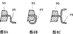
图8是外引脚邻近区域的示意部分横切面图,其中图8A显示上述的实例,图8B和8C显示其变型。Fig. 8 is a schematic partial cross-sectional view of the vicinity of the outer leads, in which Fig. 8A shows the above-mentioned example, and Figs. 8B and 8C show modifications thereof.
图8A显示第一个实例的被称作鸥翼或Z形弯角的外引脚25。图8B和8C中所示的外引脚分别被称作J形弯角和多弯角。希望的是,依照应用及安装基片,从中选择合适的外引脚构型。Figure 8A shows a first example of an
在安装半导体发光器件的工艺中,组合引线框被用来进行半导体元件的安装、引线键合、夹入模压以及树脂密封。然后引线框被切割并按需要弯曲成上述构形。从而,完成图1或3的半导体发光器件。In a process of mounting a semiconductor light emitting device, a combined lead frame is used for mounting of a semiconductor element, wire bonding, insert molding, and resin sealing. The leadframe is then cut and bent as desired into the configuration described above. Thus, the semiconductor light emitting device of FIG. 1 or 3 is completed.
在本实例中,描述了半导体发光器件,该半导体发光器件配有基于氮化物半导体的半导体发光元件。然而,该半导体发光器件可以基于其他材料。例如,基于InGaAlP或AlGaAs,半导体发光器件可以配有500到700nm频带内的半导体发光元件,即,由绿色到红色频带。In this example, a semiconductor light emitting device provided with a nitride semiconductor-based semiconductor light emitting element is described. However, the semiconductor light emitting device may be based on other materials. For example, based on InGaAlP or AlGaAs, a semiconductor light emitting device can be provided with a semiconductor light emitting element in the band of 500 to 700 nm, ie, the band from green to red.
参照附图已经描述了本发明的实施例。然而,本发明不限于此。例如,从不同方面适用于本领域技术人员的半导体发光元件的材料、形状和尺寸、构成半导体发光器件的模塑主体、树脂、填料、荧光粉以及引脚,也被包括在本发明的范畴内,只要它们不偏离本发明的精神实质。The embodiments of the present invention have been described with reference to the accompanying drawings. However, the present invention is not limited thereto. For example, materials, shapes and sizes of semiconductor light emitting elements, molding bodies, resins, fillers, phosphors and pins that are suitable for those skilled in the art from different aspects, are also included in the scope of the present invention , as long as they do not deviate from the spirit of the present invention.
Claims (12)
Translated fromChineseApplications Claiming Priority (2)
| Application Number | Priority Date | Filing Date | Title |
|---|---|---|---|
| JP2006235744AJP2008060344A (en) | 2006-08-31 | 2006-08-31 | Semiconductor light emitting device |
| JP2006235744 | 2006-08-31 |
Publications (2)
| Publication Number | Publication Date |
|---|---|
| CN101136447Atrue CN101136447A (en) | 2008-03-05 |
| CN100546061C CN100546061C (en) | 2009-09-30 |
Family
ID=39150247
Family Applications (1)
| Application Number | Title | Priority Date | Filing Date |
|---|---|---|---|
| CNB2007101483305AActiveCN100546061C (en) | 2006-08-31 | 2007-08-31 | Semiconductor light emitting device |
Country Status (4)
| Country | Link |
|---|---|
| US (1) | US7531845B2 (en) |
| JP (1) | JP2008060344A (en) |
| CN (1) | CN100546061C (en) |
| TW (1) | TWI351774B (en) |
Cited By (18)
| Publication number | Priority date | Publication date | Assignee | Title |
|---|---|---|---|---|
| CN101867008A (en)* | 2010-05-17 | 2010-10-20 | 中山大学佛山研究院 | LED packaging module capable of releasing stress |
| CN102280532A (en)* | 2010-12-08 | 2011-12-14 | 连得科技股份有限公司 | Manufacturing method of SMD double-color lead frame of light emitting diode |
| CN102290497A (en)* | 2010-10-13 | 2011-12-21 | 连得科技股份有限公司 | A kind of SMD lead frame manufacturing method of light emitting diode |
| CN102315207A (en)* | 2010-07-01 | 2012-01-11 | Lg伊诺特有限公司 | Light |
| CN102630346A (en)* | 2009-11-25 | 2012-08-08 | 欧司朗光电半导体有限公司 | Housing for an opto-electronic component and method for producing a housing |
| CN102754229A (en)* | 2010-02-09 | 2012-10-24 | 日亚化学工业株式会社 | Light emitting device and method for manufacturing light emitting device |
| CN102760816A (en)* | 2011-04-26 | 2012-10-31 | 展晶科技(深圳)有限公司 | LED (light emitting diode) packaging structure and manufacturing method thereof |
| CN101752355B (en)* | 2008-11-28 | 2012-10-31 | 夏普株式会社 | light emitting device |
| WO2012149698A1 (en)* | 2011-05-03 | 2012-11-08 | 深圳市华星光电技术有限公司 | Led package structure and liquid crystal display |
| CN102804361A (en)* | 2010-03-15 | 2012-11-28 | 欧司朗光电半导体有限公司 | Optoelectronic component and method for the production thereof |
| CN102891241A (en)* | 2012-06-21 | 2013-01-23 | 惠州雷曼光电科技有限公司 | Surface-mounted type LED (light-emitting diode) bracket, surface-mounted type LED and manufacture methods thereof |
| CN102956796A (en)* | 2011-07-15 | 2013-03-06 | 财团法人成大研究发展基金会 | Light-emitting diode crystal grain module and packaging method and removing fixture thereof |
| CN103199178A (en)* | 2009-01-30 | 2013-07-10 | 日亚化学工业株式会社 | Light emitting semiconductor device and method of manufacture thereof |
| CN103219447A (en)* | 2013-03-20 | 2013-07-24 | 深圳雷曼光电科技股份有限公司 | TOP-LED packaging device and preparation method thereof |
| CN103762292A (en)* | 2014-01-17 | 2014-04-30 | 桂林电子科技大学 | LED packaging technology for using low-light-reflection black EMC to achieve high-light-reflection effect |
| CN103460413B (en)* | 2011-04-08 | 2016-06-01 | 奥斯兰姆奥普托半导体有限责任公司 | Method for manufacturing an optoelectronic device and device thus manufactured |
| CN106449621A (en)* | 2016-10-14 | 2017-02-22 | 佛山市顺德区蚬华多媒体制品有限公司 | LED (light emitting diode) encapsulation method and structure thereof |
| CN110289341A (en)* | 2019-06-12 | 2019-09-27 | 浙江英特来光电科技有限公司 | A kind of full-color SMD LED and its installation method that increases binding force with printed circuit board |
Families Citing this family (81)
| Publication number | Priority date | Publication date | Assignee | Title |
|---|---|---|---|---|
| DE10229067B4 (en)* | 2002-06-28 | 2007-08-16 | Osram Opto Semiconductors Gmbh | Optoelectronic component and method for its production |
| KR20100037163A (en)* | 2007-07-30 | 2010-04-08 | 샤프 가부시키가이샤 | Clean room with light emitting device, lighting device and lighting device |
| US8049237B2 (en)* | 2007-12-28 | 2011-11-01 | Nichia Corporation | Light emitting device |
| KR101226777B1 (en)* | 2008-03-25 | 2013-01-25 | 가부시끼가이샤 도시바 | Light emitting device, and method and apparatus for manufacturing same |
| US20110095310A1 (en) | 2008-03-26 | 2011-04-28 | Shimane Prefectural Government | Semiconductor light emitting module and method of manufacturing the same |
| JP2009272369A (en)* | 2008-05-01 | 2009-11-19 | Nec Lighting Ltd | Light emitting device and method of manufacturing the same |
| KR20100003320A (en)* | 2008-06-24 | 2010-01-08 | 엘지이노텍 주식회사 | Light emitting diode package |
| DE102008048259B4 (en)* | 2008-09-22 | 2024-10-02 | OSRAM Opto Semiconductors Gesellschaft mit beschränkter Haftung | Housing for an optoelectronic component, side-emitting component with a housing and method for producing a housing |
| CN102265417B (en)* | 2008-12-26 | 2013-10-23 | 古河电气工业株式会社 | Lead frame for optical semiconductor device, manufacturing method thereof, and optical semiconductor device |
| KR20100080423A (en)* | 2008-12-30 | 2010-07-08 | 삼성엘이디 주식회사 | Light emitting device package and method of fabricating thereof |
| JP2010161139A (en)* | 2009-01-07 | 2010-07-22 | Toshiba Corp | Light emitting device |
| JP2010177443A (en)* | 2009-01-29 | 2010-08-12 | Showa Denko Kk | Light-emitting device and light-emitting module |
| JP2014158052A (en)* | 2009-01-30 | 2014-08-28 | Nichia Chem Ind Ltd | Light emitting device and method of manufacturing the same |
| DE102009025266B4 (en)* | 2009-06-17 | 2015-08-20 | Osram Opto Semiconductors Gmbh | Optoelectronic semiconductor device |
| KR101117616B1 (en) | 2009-10-15 | 2012-03-09 | 주식회사 이츠웰 | Light-emitting diode package |
| JP2011096793A (en)* | 2009-10-29 | 2011-05-12 | Nichia Corp | Light-emitting device |
| CN106449937B (en)* | 2009-10-29 | 2020-11-03 | 日亚化学工业株式会社 | Light emitting device and method for manufacturing the same |
| CN102714267B (en)* | 2009-11-19 | 2015-05-20 | 住友化学株式会社 | Package for semiconductor, and heat dissipating lead frame |
| US8525213B2 (en)* | 2010-03-30 | 2013-09-03 | Lg Innotek Co., Ltd. | Light emitting device having multiple cavities and light unit having the same |
| TWI509838B (en)* | 2010-04-14 | 2015-11-21 | Pang Ming Huang | Light-emitting diode housing with surface coating of fluorinated polymer and light-emitting diode structure thereof |
| JPWO2011136356A1 (en)* | 2010-04-30 | 2013-07-22 | ローム株式会社 | LED module |
| JP5535750B2 (en) | 2010-04-30 | 2014-07-02 | ローム株式会社 | Light emitting element module |
| US20130043502A1 (en)* | 2010-05-31 | 2013-02-21 | Panasonic Corporation | Light emitting device and method for manufacturing the same |
| DE102010024864B4 (en) | 2010-06-24 | 2021-01-21 | OSRAM Opto Semiconductors Gesellschaft mit beschränkter Haftung | Optoelectronic semiconductor component |
| KR101832536B1 (en) | 2010-08-31 | 2018-02-26 | 니치아 카가쿠 고교 가부시키가이샤 | Light emitting device and method for manufacturing same |
| JP5644352B2 (en)* | 2010-10-15 | 2014-12-24 | 日亜化学工業株式会社 | Light emitting device and manufacturing method thereof |
| JP5886584B2 (en)* | 2010-11-05 | 2016-03-16 | ローム株式会社 | Semiconductor light emitting device |
| KR101230622B1 (en)* | 2010-12-10 | 2013-02-06 | 이정훈 | Method of fabricating semiconductor device using gang bonding and semiconductor device fabricated by the same |
| JP5582048B2 (en)* | 2011-01-28 | 2014-09-03 | 日亜化学工業株式会社 | Light emitting device |
| KR20120093679A (en)* | 2011-02-15 | 2012-08-23 | 삼성전자주식회사 | Light emitting device package and manufacturing method thereof |
| CN102683543B (en)* | 2011-03-15 | 2015-08-12 | 展晶科技(深圳)有限公司 | LED encapsulation structure |
| JP5724573B2 (en)* | 2011-04-19 | 2015-05-27 | 日亜化学工業株式会社 | Light emitting device |
| JP2014011029A (en)* | 2012-06-29 | 2014-01-20 | Toshiba Lighting & Technology Corp | Lighting apparatus |
| CN102881800A (en)* | 2011-07-15 | 2013-01-16 | 展晶科技(深圳)有限公司 | Light emitting diode packaging structure and manufacturing method thereof |
| WO2013011628A1 (en)* | 2011-07-19 | 2013-01-24 | パナソニック株式会社 | Light emitting device and method for manufacturing same |
| JP5848114B2 (en)* | 2011-12-20 | 2016-01-27 | スタンレー電気株式会社 | Light emitting device |
| JP6078948B2 (en) | 2012-01-20 | 2017-02-15 | 日亜化学工業株式会社 | Package molded body for light emitting device and light emitting device using the same |
| EP2879195A4 (en)* | 2012-07-27 | 2016-01-20 | Konica Minolta Inc | LED DEVICE AND METHOD OF MANUFACTURING THE SAME |
| JP6001956B2 (en)* | 2012-08-10 | 2016-10-05 | 株式会社東芝 | Semiconductor device |
| JP6171295B2 (en)* | 2012-09-27 | 2017-08-02 | 日亜化学工業株式会社 | Light emitting device |
| JP6056336B2 (en)* | 2012-09-28 | 2017-01-11 | 日亜化学工業株式会社 | Light emitting device |
| JP2016518033A (en) | 2013-05-15 | 2016-06-20 | コーニンクレッカ フィリップス エヌ ヴェKoninklijke Philips N.V. | Light emitting device using optical element and reflector |
| JP6221403B2 (en) | 2013-06-26 | 2017-11-01 | 日亜化学工業株式会社 | Light emitting device |
| JP6232792B2 (en)* | 2013-07-17 | 2017-11-22 | 日亜化学工業株式会社 | Light emitting device |
| US9257616B2 (en) | 2013-08-27 | 2016-02-09 | Glo Ab | Molded LED package and method of making same |
| US9142745B2 (en)* | 2013-08-27 | 2015-09-22 | Glo Ab | Packaged LED device with castellations |
| JP6237174B2 (en) | 2013-12-05 | 2017-11-29 | 日亜化学工業株式会社 | Light emitting device |
| JP6621990B2 (en)* | 2014-01-16 | 2019-12-18 | スタンレー電気株式会社 | Ultraviolet light emitting diode |
| JP2015225942A (en)* | 2014-05-28 | 2015-12-14 | サンケン電気株式会社 | Light emitting device |
| JP6369266B2 (en)* | 2014-09-30 | 2018-08-08 | 日亜化学工業株式会社 | LIGHT EMITTING DEVICE AND LIGHT EMITTING DEVICE MANUFACTURING METHOD |
| KR101888608B1 (en)* | 2014-10-17 | 2018-09-20 | 엘지이노텍 주식회사 | Light emitting device package and lighting apparatus |
| JP5949875B2 (en)* | 2014-11-06 | 2016-07-13 | 日亜化学工業株式会社 | Light emitting device and manufacturing method thereof |
| JP2016100385A (en)* | 2014-11-19 | 2016-05-30 | パイオニア株式会社 | Optical semiconductor device and optical semiconductor device manufacturing method |
| JP6206442B2 (en) | 2015-04-30 | 2017-10-04 | 日亜化学工業株式会社 | Package, method for manufacturing the same, and light emitting device |
| JP6332342B2 (en)* | 2015-08-20 | 2018-05-30 | 日亜化学工業株式会社 | LIGHT EMITTING DEVICE AND LIGHT EMITTING DEVICE MANUFACTURING METHOD |
| US9859480B2 (en) | 2015-08-20 | 2018-01-02 | Nichia Corporation | Light emitting device and method of manufacturing light emitting device |
| US9865779B2 (en) | 2015-09-30 | 2018-01-09 | Nichia Corporation | Methods of manufacturing the package and light-emitting device |
| JP6536325B2 (en)* | 2015-09-30 | 2019-07-03 | 日亜化学工業株式会社 | Light emitting device |
| EP3174088B1 (en)* | 2015-11-26 | 2020-12-30 | Siyang Grande Electronics Co., Ltd. | Method of manufacturing a plastic packaged smd diode |
| JP6728676B2 (en)* | 2015-12-26 | 2020-07-22 | 日亜化学工業株式会社 | Light emitting device |
| JP6213582B2 (en)* | 2016-01-22 | 2017-10-18 | 日亜化学工業株式会社 | Light emitting device |
| US10403792B2 (en) | 2016-03-07 | 2019-09-03 | Rayvio Corporation | Package for ultraviolet emitting devices |
| JP6533766B2 (en)* | 2016-09-07 | 2019-06-19 | 日亜化学工業株式会社 | Package molded body for light emitting device and light emitting device using the same |
| JP6493348B2 (en)* | 2016-09-30 | 2019-04-03 | 日亜化学工業株式会社 | Light emitting device |
| JP6555243B2 (en) | 2016-12-16 | 2019-08-07 | 日亜化学工業株式会社 | Light emitting device and method for manufacturing light emitting device |
| JP6555242B2 (en) | 2016-12-16 | 2019-08-07 | 日亜化学工業株式会社 | Light emitting device and method for manufacturing light emitting device |
| US10411169B2 (en) | 2017-02-03 | 2019-09-10 | Nichia Corporation | Light emitting device having leads in resin package |
| US10854787B2 (en)* | 2017-08-03 | 2020-12-01 | Osam Oled Gmbh | Component having boundary element |
| JP7064325B2 (en)* | 2017-12-18 | 2022-05-10 | スタンレー電気株式会社 | A semiconductor light emitting device and a method for manufacturing a semiconductor light emitting device using the semiconductor light emitting device. |
| JP7139111B2 (en)* | 2017-12-22 | 2022-09-20 | スタンレー電気株式会社 | Light emitting device and manufacturing method thereof |
| WO2020003789A1 (en)* | 2018-06-29 | 2020-01-02 | 日亜化学工業株式会社 | Method for producing light emitting device, and light emitting device |
| CN111384228B (en)* | 2018-12-28 | 2024-12-03 | 日亚化学工业株式会社 | Light emitting device and method for manufacturing light emitting device |
| JP2019087763A (en)* | 2019-03-01 | 2019-06-06 | パイオニア株式会社 | Optical semiconductor device and optical semiconductor device manufacturing method |
| EP3987582A4 (en)* | 2019-06-19 | 2023-10-04 | Jade Bird Display (Shanghai) Limited | Systems and methods for multi-color led pixel unit |
| DE102019211550A1 (en) | 2019-08-01 | 2021-02-04 | OSRAM Opto Semiconductors Gesellschaft mit beschränkter Haftung | HOUSING FOR A RADIATION-EMITTING COMPONENT, METHOD FOR MANUFACTURING A RADIATION-EMITTING COMPONENT AND RADIATION-EMITTING COMPONENT |
| US12074151B2 (en) | 2020-06-03 | 2024-08-27 | Jade Bird Display (shanghai) Limited | Systems and methods for multi-color LED pixel unit with vertical light emission |
| US12176333B2 (en) | 2021-06-24 | 2024-12-24 | Hefei Boe Optoelectronics Technology Co., Ltd. | Backplane and method for manufacturing the same, backlight module, and display apparatus |
| US12237451B2 (en) | 2022-01-28 | 2025-02-25 | Creeled, Inc. | Arrangements of light-altering coatings in light-emitting diode packages |
| US20230282786A1 (en)* | 2022-03-04 | 2023-09-07 | Creeled, Inc. | Encapsulation arrangements in light-emitting diode packages |
| JP7469722B2 (en)* | 2022-07-08 | 2024-04-17 | 日亜化学工業株式会社 | Light emitting device manufacturing method and light emitting device |
| EP4464933A1 (en)* | 2023-05-18 | 2024-11-20 | Toshiba Lighting & Technology Corporation | Vehicle lighting device, vehicle lamp, and method for manufacturing vehicle lighting device |
Family Cites Families (13)
| Publication number | Priority date | Publication date | Assignee | Title |
|---|---|---|---|---|
| AT410266B (en)* | 2000-12-28 | 2003-03-25 | Tridonic Optoelectronics Gmbh | LIGHT SOURCE WITH A LIGHT-EMITTING ELEMENT |
| US6737681B2 (en)* | 2001-08-22 | 2004-05-18 | Nichia Corporation | Light emitting device with fluorescent member excited by semiconductor light emitting element |
| JPWO2003034508A1 (en)* | 2001-10-12 | 2005-02-03 | 日亜化学工業株式会社 | Light emitting device and manufacturing method thereof |
| US7258816B2 (en)* | 2002-03-22 | 2007-08-21 | Nichia Corporation | Nitride phosphor and method for preparation thereof, and light emitting device |
| JP2003282935A (en)* | 2002-03-26 | 2003-10-03 | Sharp Corp | Optical coupling element, method for manufacturing the same, and electronic device |
| DE10229067B4 (en)* | 2002-06-28 | 2007-08-16 | Osram Opto Semiconductors Gmbh | Optoelectronic component and method for its production |
| JP3655267B2 (en)* | 2002-07-17 | 2005-06-02 | 株式会社東芝 | Semiconductor light emitting device |
| US20040156195A1 (en)* | 2002-10-16 | 2004-08-12 | Robertson Jonas J. | Illuminated acrylic flashlight and tool chest light utility light |
| US20050133808A1 (en)* | 2003-09-11 | 2005-06-23 | Kyocera Corporation | Package for housing light-emitting element, light-emitting apparatus and illumination apparatus |
| JP4493013B2 (en) | 2003-10-08 | 2010-06-30 | 日亜化学工業株式会社 | Semiconductor device |
| JP3895362B2 (en)* | 2004-01-29 | 2007-03-22 | 松下電器産業株式会社 | LED lighting source |
| JP4574248B2 (en)* | 2004-06-28 | 2010-11-04 | 京セラ株式会社 | LIGHT EMITTING DEVICE AND LIGHTING DEVICE USING THE SAME |
| JP4757477B2 (en)* | 2004-11-04 | 2011-08-24 | 株式会社 日立ディスプレイズ | Light source unit, illumination device using the same, and display device using the same |
- 2006
- 2006-08-31JPJP2006235744Apatent/JP2008060344A/enactivePending
- 2007
- 2007-06-19USUS11/765,077patent/US7531845B2/enactiveActive
- 2007-08-30TWTW096132266Apatent/TWI351774B/enactive
- 2007-08-31CNCNB2007101483305Apatent/CN100546061C/enactiveActive
Cited By (25)
| Publication number | Priority date | Publication date | Assignee | Title |
|---|---|---|---|---|
| CN101752355B (en)* | 2008-11-28 | 2012-10-31 | 夏普株式会社 | light emitting device |
| CN103199178B (en)* | 2009-01-30 | 2016-12-28 | 日亚化学工业株式会社 | Semiconductor light-emitting apparatus and the manufacture method of semiconductor light-emitting apparatus |
| CN103199178A (en)* | 2009-01-30 | 2013-07-10 | 日亚化学工业株式会社 | Light emitting semiconductor device and method of manufacture thereof |
| CN102630346A (en)* | 2009-11-25 | 2012-08-08 | 欧司朗光电半导体有限公司 | Housing for an opto-electronic component and method for producing a housing |
| US9006773B2 (en) | 2009-11-25 | 2015-04-14 | Osram Opto Semiconductors Gmbh | Housing for an optoelectronic component and method for producing a housing |
| CN102754229A (en)* | 2010-02-09 | 2012-10-24 | 日亚化学工业株式会社 | Light emitting device and method for manufacturing light emitting device |
| CN102804361B (en)* | 2010-03-15 | 2016-02-24 | 欧司朗光电半导体有限公司 | Optoelectronic device and manufacturing method therefor |
| CN102804361A (en)* | 2010-03-15 | 2012-11-28 | 欧司朗光电半导体有限公司 | Optoelectronic component and method for the production thereof |
| CN101867008B (en)* | 2010-05-17 | 2012-11-21 | 中山大学佛山研究院 | LED packaging module capable of releasing stress |
| CN101867008A (en)* | 2010-05-17 | 2010-10-20 | 中山大学佛山研究院 | LED packaging module capable of releasing stress |
| CN102315207A (en)* | 2010-07-01 | 2012-01-11 | Lg伊诺特有限公司 | Light |
| CN102315207B (en)* | 2010-07-01 | 2015-11-25 | Lg伊诺特有限公司 | Light emitting device package |
| CN102290497A (en)* | 2010-10-13 | 2011-12-21 | 连得科技股份有限公司 | A kind of SMD lead frame manufacturing method of light emitting diode |
| CN102280532A (en)* | 2010-12-08 | 2011-12-14 | 连得科技股份有限公司 | Manufacturing method of SMD double-color lead frame of light emitting diode |
| CN103460413B (en)* | 2011-04-08 | 2016-06-01 | 奥斯兰姆奥普托半导体有限责任公司 | Method for manufacturing an optoelectronic device and device thus manufactured |
| CN102760816A (en)* | 2011-04-26 | 2012-10-31 | 展晶科技(深圳)有限公司 | LED (light emitting diode) packaging structure and manufacturing method thereof |
| WO2012149698A1 (en)* | 2011-05-03 | 2012-11-08 | 深圳市华星光电技术有限公司 | Led package structure and liquid crystal display |
| CN102956796A (en)* | 2011-07-15 | 2013-03-06 | 财团法人成大研究发展基金会 | Light-emitting diode crystal grain module and packaging method and removing fixture thereof |
| CN102891241B (en)* | 2012-06-21 | 2015-07-08 | 惠州雷曼光电科技有限公司 | Surface-mounted type LED (light-emitting diode) bracket, surface-mounted type LED and manufacture methods thereof |
| CN102891241A (en)* | 2012-06-21 | 2013-01-23 | 惠州雷曼光电科技有限公司 | Surface-mounted type LED (light-emitting diode) bracket, surface-mounted type LED and manufacture methods thereof |
| CN103219447A (en)* | 2013-03-20 | 2013-07-24 | 深圳雷曼光电科技股份有限公司 | TOP-LED packaging device and preparation method thereof |
| CN103219447B (en)* | 2013-03-20 | 2016-05-25 | 深圳雷曼光电科技股份有限公司 | TOP-LED packaging and preparation method thereof |
| CN103762292A (en)* | 2014-01-17 | 2014-04-30 | 桂林电子科技大学 | LED packaging technology for using low-light-reflection black EMC to achieve high-light-reflection effect |
| CN106449621A (en)* | 2016-10-14 | 2017-02-22 | 佛山市顺德区蚬华多媒体制品有限公司 | LED (light emitting diode) encapsulation method and structure thereof |
| CN110289341A (en)* | 2019-06-12 | 2019-09-27 | 浙江英特来光电科技有限公司 | A kind of full-color SMD LED and its installation method that increases binding force with printed circuit board |
Also Published As
| Publication number | Publication date |
|---|---|
| JP2008060344A (en) | 2008-03-13 |
| CN100546061C (en) | 2009-09-30 |
| TWI351774B (en) | 2011-11-01 |
| TW200824154A (en) | 2008-06-01 |
| US20080054287A1 (en) | 2008-03-06 |
| US7531845B2 (en) | 2009-05-12 |
Similar Documents
| Publication | Publication Date | Title |
|---|---|---|
| US7531845B2 (en) | Semiconductor light emitting device | |
| KR100978028B1 (en) | Light emitting device | |
| CN100463238C (en) | Semiconductor light emitting device, manufacturing method thereof, and semiconductor light emitting component | |
| KR100809210B1 (en) | High output LED package and manufacturing method | |
| JP6323217B2 (en) | Light emitting device | |
| CN103400929B (en) | Light-emitting device and manufacture method thereof | |
| US10411178B2 (en) | Light emitting device | |
| JPH10261821A (en) | Semiconductor light emitting device and method of manufacturing the same | |
| US9893258B2 (en) | Package, light emitting device, and methods of manufacturing the package and the light emitting device | |
| CN104078551A (en) | Light emitting device and method of manufacturing the same | |
| JP2001024228A (en) | Light emitting device | |
| JP2002094128A (en) | Light emitting diode and method of manufacturing the same | |
| KR100849828B1 (en) | Light emitting diode package | |
| JP4206334B2 (en) | Light emitting device | |
| JP4254214B2 (en) | Semiconductor device and manufacturing method thereof | |
| TW202123507A (en) | Led light emitting device and manufacturing method therefor | |
| US12289933B2 (en) | Semiconductor light-emitting device and manufacturing method of the same | |
| CN103227264B (en) | Light-emitting device | |
| JP2025099548A (en) | Light-emitting device | |
| CN106711307A (en) | Frame for semiconductor light emitting device | |
| JP2023033028A (en) | Light-emitting device | |
| JP2006073912A (en) | Semiconductor light emitting device and manufacturing method thereof | |
| KR20120069071A (en) | Light emitting device |
Legal Events
| Date | Code | Title | Description |
|---|---|---|---|
| C06 | Publication | ||
| PB01 | Publication | ||
| C10 | Entry into substantive examination | ||
| SE01 | Entry into force of request for substantive examination | ||
| C14 | Grant of patent or utility model | ||
| GR01 | Patent grant | ||
| TR01 | Transfer of patent right | Effective date of registration:20180315 Address after:Tokyo, Japan Co-patentee after:Toyoda Gosei Co., Ltd. Patentee after:Toshiba electronic components and storage plant Address before:Tokyo, Japan, Japan Co-patentee before:Toyoda Gosei Co., Ltd. Patentee before:Toshiba Corp | |
| TR01 | Transfer of patent right |