CN101120122B - Gas distribution showerhead featuring exhaust apertures - Google Patents
Gas distribution showerhead featuring exhaust aperturesDownload PDFInfo
- Publication number
- CN101120122B CN101120122BCN2004800339871ACN200480033987ACN101120122BCN 101120122 BCN101120122 BCN 101120122BCN 2004800339871 ACN2004800339871 ACN 2004800339871ACN 200480033987 ACN200480033987 ACN 200480033987ACN 101120122 BCN101120122 BCN 101120122B
- Authority
- CN
- China
- Prior art keywords
- exhaust
- gas
- process gas
- wafer
- deposition chamber
- Prior art date
- Legal status (The legal status is an assumption and is not a legal conclusion. Google has not performed a legal analysis and makes no representation as to the accuracy of the status listed.)
- Expired - Fee Related
Links
Images


Classifications
- C—CHEMISTRY; METALLURGY
- C23—COATING METALLIC MATERIAL; COATING MATERIAL WITH METALLIC MATERIAL; CHEMICAL SURFACE TREATMENT; DIFFUSION TREATMENT OF METALLIC MATERIAL; COATING BY VACUUM EVAPORATION, BY SPUTTERING, BY ION IMPLANTATION OR BY CHEMICAL VAPOUR DEPOSITION, IN GENERAL; INHIBITING CORROSION OF METALLIC MATERIAL OR INCRUSTATION IN GENERAL
- C23C—COATING METALLIC MATERIAL; COATING MATERIAL WITH METALLIC MATERIAL; SURFACE TREATMENT OF METALLIC MATERIAL BY DIFFUSION INTO THE SURFACE, BY CHEMICAL CONVERSION OR SUBSTITUTION; COATING BY VACUUM EVAPORATION, BY SPUTTERING, BY ION IMPLANTATION OR BY CHEMICAL VAPOUR DEPOSITION, IN GENERAL
- C23C16/00—Chemical coating by decomposition of gaseous compounds, without leaving reaction products of surface material in the coating, i.e. chemical vapour deposition [CVD] processes
- C23C16/44—Chemical coating by decomposition of gaseous compounds, without leaving reaction products of surface material in the coating, i.e. chemical vapour deposition [CVD] processes characterised by the method of coating
- C23C16/455—Chemical coating by decomposition of gaseous compounds, without leaving reaction products of surface material in the coating, i.e. chemical vapour deposition [CVD] processes characterised by the method of coating characterised by the method used for introducing gases into reaction chamber or for modifying gas flows in reaction chamber
- C—CHEMISTRY; METALLURGY
- C23—COATING METALLIC MATERIAL; COATING MATERIAL WITH METALLIC MATERIAL; CHEMICAL SURFACE TREATMENT; DIFFUSION TREATMENT OF METALLIC MATERIAL; COATING BY VACUUM EVAPORATION, BY SPUTTERING, BY ION IMPLANTATION OR BY CHEMICAL VAPOUR DEPOSITION, IN GENERAL; INHIBITING CORROSION OF METALLIC MATERIAL OR INCRUSTATION IN GENERAL
- C23C—COATING METALLIC MATERIAL; COATING MATERIAL WITH METALLIC MATERIAL; SURFACE TREATMENT OF METALLIC MATERIAL BY DIFFUSION INTO THE SURFACE, BY CHEMICAL CONVERSION OR SUBSTITUTION; COATING BY VACUUM EVAPORATION, BY SPUTTERING, BY ION IMPLANTATION OR BY CHEMICAL VAPOUR DEPOSITION, IN GENERAL
- C23C16/00—Chemical coating by decomposition of gaseous compounds, without leaving reaction products of surface material in the coating, i.e. chemical vapour deposition [CVD] processes
- C23C16/44—Chemical coating by decomposition of gaseous compounds, without leaving reaction products of surface material in the coating, i.e. chemical vapour deposition [CVD] processes characterised by the method of coating
- C23C16/4412—Details relating to the exhausts, e.g. pumps, filters, scrubbers, particle traps
- C—CHEMISTRY; METALLURGY
- C23—COATING METALLIC MATERIAL; COATING MATERIAL WITH METALLIC MATERIAL; CHEMICAL SURFACE TREATMENT; DIFFUSION TREATMENT OF METALLIC MATERIAL; COATING BY VACUUM EVAPORATION, BY SPUTTERING, BY ION IMPLANTATION OR BY CHEMICAL VAPOUR DEPOSITION, IN GENERAL; INHIBITING CORROSION OF METALLIC MATERIAL OR INCRUSTATION IN GENERAL
- C23C—COATING METALLIC MATERIAL; COATING MATERIAL WITH METALLIC MATERIAL; SURFACE TREATMENT OF METALLIC MATERIAL BY DIFFUSION INTO THE SURFACE, BY CHEMICAL CONVERSION OR SUBSTITUTION; COATING BY VACUUM EVAPORATION, BY SPUTTERING, BY ION IMPLANTATION OR BY CHEMICAL VAPOUR DEPOSITION, IN GENERAL
- C23C16/00—Chemical coating by decomposition of gaseous compounds, without leaving reaction products of surface material in the coating, i.e. chemical vapour deposition [CVD] processes
- C23C16/44—Chemical coating by decomposition of gaseous compounds, without leaving reaction products of surface material in the coating, i.e. chemical vapour deposition [CVD] processes characterised by the method of coating
- C23C16/455—Chemical coating by decomposition of gaseous compounds, without leaving reaction products of surface material in the coating, i.e. chemical vapour deposition [CVD] processes characterised by the method of coating characterised by the method used for introducing gases into reaction chamber or for modifying gas flows in reaction chamber
- C23C16/45563—Gas nozzles
- C23C16/45565—Shower nozzles
Landscapes
- Chemical & Material Sciences (AREA)
- General Chemical & Material Sciences (AREA)
- Chemical Kinetics & Catalysis (AREA)
- Engineering & Computer Science (AREA)
- Materials Engineering (AREA)
- Mechanical Engineering (AREA)
- Metallurgy (AREA)
- Organic Chemistry (AREA)
- Chemical Vapour Deposition (AREA)
- Drying Of Semiconductors (AREA)
Abstract
Translated fromChinese
Description
Translated fromChinese技术领域technical field
本发明一般是与半导体晶片制程系统有关,更明确而言,是关于在工件表面分布制程气体的系统与方法。The present invention relates generally to semiconductor wafer processing systems, and more particularly to systems and methods for distributing process gases over workpiece surfaces.
背景技术Background technique
半导体晶片制程系统通常含有一制程室,其具有晶座或基座,用以于制程室内靠近制程区域支撑半导体晶片。制程室形成一真空范围,界定出部分的制程区域。一气体散流组件或喷气头可提供一或多个制程气体至制程区域。接着可加热及/或提供能量予该气体以形成一等离子体,于晶片上实施特定制程。这些制程可包含化学气相沉积(Chemical Vapor Deposition,CVD),以沉积薄膜于晶片上,或一蚀刻反应以由晶片移除材料。A semiconductor wafer processing system generally includes a processing chamber having a pedestal or pedestal for supporting a semiconductor wafer near a processing area within the processing chamber. The process chamber forms a vacuum range to define a part of the process area. A gas distribution assembly or gas sparger provides one or more process gases to the process area. The gas can then be heated and/or energized to form a plasma to perform specific processes on the wafer. These processes may include Chemical Vapor Deposition (CVD) to deposit thin films on the wafer, or an etching reaction to remove material from the wafer.
随着半导体装置尺寸与复杂度的增加,晶片面积变为更加珍贵。因此,不仅希望将元件设置至靠近晶片中心,亦希望尽可能靠近晶片外部边缘。将元件设置在靠近晶片周围处也提高了在径向范围中晶片制程步骤的的一致性(radial uniformity)的要求。因此,是希望半导体制造过程可几乎于整个晶片表面达到一致性。As semiconductor devices increase in size and complexity, die area becomes more precious. Therefore, it is desirable not only to locate components as close to the center of the wafer as possible, but also as close as possible to the outer edge of the wafer. Locating the components close to the wafer perimeter also raises the requirement for radial uniformity of the wafer processing steps in the radial range. Therefore, it is desirable for semiconductor manufacturing processes to achieve uniformity over nearly the entire wafer surface.
图2显示习知技艺的沉积室210,具有习知技艺的喷气头220。习知技艺的喷气头220特征为,于喷气头下表面225具有数个相等间隔的孔洞222。制程气体经由入口导管214,沿标记方向215流入喷气头220。孔洞222用以于喷气头内沿方向218分布制程气体。制程气体经由孔洞222离开喷气头,并与半导体晶片230表面反应。喷气头内的气体空间散流,决定分布于半导体晶片表面气体的一致性。FIG. 2 shows a prior
于沉积制程中,制程气体流经半导体晶片230的顶部表面235,并与表面235或其他气态物种反应,以于晶片表面235形成所需的薄膜236。气体于晶片边缘沿方向238流动,并经由环状排气通道250排气。During the deposition process, process gases flow over the
于图2所绘示的习知技艺沉积室,为抵达排气通道250,于晶片中心上方,由喷气头所引入的制程气体,通常于径向方向沿晶片表面流动,且于晶片边缘沿方向238流动。因此,当气体于径向方向朝向晶片边缘流动时,气态物种的速度便可能增加。In the prior art deposition chamber shown in FIG. 2 , in order to reach the
于沉积制程中,沉积速率典型地取决于反应种类相对于半导体晶片表面的流动。若反应种类的速度于径向方向上增加,沉积速率于靠近晶片周围可能大于靠近晶片中心,导致不一致的薄膜厚度。In a deposition process, the deposition rate typically depends on the flow of reactive species relative to the semiconductor wafer surface. If the velocity of the reactive species increases in the radial direction, the deposition rate may be greater near the periphery of the wafer than near the center of the wafer, resulting in inconsistent film thickness.
因此,业界亟需一种设备是可改进沉积于半导体晶片的薄膜的一致性。Therefore, there is a need in the industry for an apparatus that can improve the consistency of thin films deposited on semiconductor wafers.
发明内容Contents of the invention
根据本发明的具体实施例,是关于在工件表面分布制程气体的系统与方法。根据本发明一具体实施例,制程气体由一来源,经由具有数个孔隙的气体散流喷气头,流至工件表面。气体散流喷气头亦具有数个排气孔隙特征,以移除来自晶片表面上的材料。由喷气头排气孔隙所提供的补充排气,是用以减少由于通过晶片表面的径向流动所产生的气体速度变化,从而增强相对于晶片中心的晶片边缘的处理一致性。Embodiments of the present invention relate to systems and methods for distributing process gases over a surface of a workpiece. According to an embodiment of the present invention, the process gas flows from a source to the surface of the workpiece through a gas distribution nozzle having a plurality of holes. The gas dispersion showerhead also features several vent apertures to remove material from the wafer surface. Supplemental exhaust provided by the jet head exhaust aperture is used to reduce gas velocity variations due to radial flow across the wafer surface, thereby enhancing process uniformity at the wafer edge relative to the wafer center.
根据本发明一具体实施例的设备,包含围绕制程室的侧壁,以及位于制程室内的晶片基座。第一排气导管与制程室进行流体交换,且一制程气体源经由气体散流喷气头而与制程室进行流体交换。气体散流喷气头含有一第一通道其可与制程气体源进行流体交换,以及分布于该喷气头下表面的孔隙;以及与第一通道分隔的一第二通道,其与第二排气导管,以及分布于喷气头下表面的排气孔隙,进行流体交换。An apparatus according to an embodiment of the present invention includes side walls surrounding a process chamber, and a wafer susceptor within the process chamber. The first exhaust conduit is in fluid communication with the process chamber, and a process gas source is in fluid communication with the process chamber through the gas diffuser nozzle. The gas dispersion showerhead includes a first channel which is fluidly communicated with a source of process gas and pores distributed on the lower surface of the showerhead; and a second channel separate from the first channel and connected to the second exhaust conduit , and the exhaust pores distributed on the lower surface of the nozzle for fluid exchange.
根据本发明一具体实施例,以处理半导体工件的方法是包含,经由位于气体散流面板的第一数个孔隙,流动一制程气体至一半导体工件。气体由半导体工件上,经由制程室排气通道,以及位于气体散流面板的第二数个孔隙而移除。According to an embodiment of the present invention, a method for processing a semiconductor workpiece includes flowing a process gas to a semiconductor workpiece through a first plurality of apertures in a gas distribution panel. Gas is removed from the semiconductor workpiece through the chamber exhaust channel and the second plurality of apertures in the gas diffuser panel.
根据本发明一具体实施例,以于一制程室处理半导体晶片的方法是包含,置入一半导体晶片至制程室,并经由第一排气通道排空制程室。至少一制程气体,经由位于喷气头表面的第一组孔隙引入。气体经由第一排气通道移除,且气体经由位于喷气头表面的数个孔隙移除。According to an embodiment of the present invention, a method for processing a semiconductor wafer in a process chamber includes placing a semiconductor wafer into the process chamber, and evacuating the process chamber through a first exhaust channel. At least one process gas is introduced through a first set of apertures located on the surface of the shower head. The gas is removed through the first exhaust channel, and the gas is removed through several pores located on the surface of the gas shower head.
根据本发明一具体实施例,以控制沉积于半导体晶片上薄膜性质一致性的方法是包含,放置一晶片于一制程室,并经由位于面板的第一数个孔隙,引入气体至晶片。气体经由位于面板的第二数个孔隙移除,且气体同时由径向排气路径移除。According to an embodiment of the present invention, a method for controlling the uniformity of properties of a thin film deposited on a semiconductor wafer includes placing a wafer in a process chamber and introducing gas to the wafer through a first plurality of apertures located in a panel. The gas is removed through the second number of apertures located in the panel, and the gas is simultaneously removed by the radial exhaust path.
本发明的这些与其他具体实施例,以及其特征与一些潜在优点,将连同随后的内容与所附图示详细描述。These and other specific embodiments of the invention, together with their features and some potential advantages, will be described in detail in conjunction with what follows and the accompanying figures.
附图说明Description of drawings
图1A为化学气相沉积系统的一简化概要图示。Figure 1A is a simplified schematic diagram of a chemical vapor deposition system.
图1B为化学气相沉积系统制程室侧壁部分,分解透视的简化概要图示。FIG. 1B is a simplified schematic illustration of an exploded perspective view of a side wall portion of a chemical vapor deposition system process chamber.
图1C为化学气相沉积系统制程室盖子组件,分解透视的简化概要图示。Figure 1C is a simplified schematic illustration of a chemical vapor deposition system process chamber lid assembly, exploded perspective.
图2为习知技艺的沉积室与喷气头简化概要图示。Figure 2 is a simplified schematic diagram of a prior art deposition chamber and gas showerhead.
图3A为根据本发明一具体实施例的沉积室简化概要图示。Figure 3A is a simplified schematic diagram of a deposition chamber according to an embodiment of the invention.
图3B为根据本发明另一具体实施例的沉积室简化概要图示。3B is a simplified schematic diagram of a deposition chamber according to another embodiment of the invention.
图3C为根据本发明额外具体实施例的沉积室简化概要图示。3C is a simplified schematic illustration of a deposition chamber according to additional embodiments of the invention.
图4A为根据本发明一具体实施例的喷气头简化侧边截面图示。4A is a simplified side cross-sectional illustration of an air shower head in accordance with an embodiment of the present invention.
图4B为根据本发明一具体实施例的喷气头简化仰视图示。Figure 4B is a simplified bottom view illustration of an air shower head in accordance with an embodiment of the present invention.
图4C为喷气头的一简化仰视图示,说明仰视图示间的关系。Figure 4C is a simplified bottom view illustration of an air shower head illustrating the relationship between the bottom view illustrations.
图4CA为图4C所示喷气头底面部分的放大图示。FIG. 4CA is an enlarged view of a portion of the bottom surface of the spray head shown in FIG. 4C.
图5为根据本发明另一具体实施例的喷气头简化仰视图示。Figure 5 is a simplified bottom view illustration of an air jet head according to another embodiment of the invention.
图6为根据本发明一具体实施例的喷气头径向截面简化仰视图示。Figure 6 is a simplified bottom view illustration of a radial cross-section of an air injection head in accordance with an embodiment of the present invention.
图7为根据本发明另一具体实施例的喷气头径向截面简化仰视图示。7 is a simplified bottom view illustration of a radial section of an air injection head according to another embodiment of the present invention.
图8为根据本发明另一具体实施例的喷气头径向截面简化仰视图示。8 is a simplified bottom view illustration of a radial section of an air injection head according to another embodiment of the present invention.
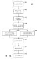
图9A为一流程图示,绘示根据本发明操作沉积室的一具体实施例方法。Figure 9A is a flow diagram illustrating an embodiment method of operating a deposition chamber in accordance with the present invention.
图9B为一流程图示,绘示根据本发明操作沉积室的另一具体实施例方法。9B is a flow diagram illustrating another embodiment method of operating a deposition chamber in accordance with the present invention.
图9C为一流程图示,绘示根据本发明操作沉积室的再另一具体实施例方法。9C is a flow diagram illustrating yet another embodiment method of operating a deposition chamber in accordance with the present invention.
具体实施方式Detailed ways
根据本发明的具体实施例,是关于在工件表面分布制程气体的系统与方法。根据本发明一具体实施例,制程气体由一来源,经由具有数个孔隙的一气体散流喷气头,流动至一工件表面。气体散流喷气头亦具有数个排气孔隙的特征,以由晶片表面移除材料。由喷气头排气孔隙提供的补充排气,是用于减少通过晶片表面的径向流动,所造成的气体速度变化,从而增强相对于晶片中心的晶片边缘的处理一致性。Embodiments of the present invention relate to systems and methods for distributing process gases over a surface of a workpiece. According to an embodiment of the present invention, process gas flows from a source to a surface of a workpiece through a gas diffuser nozzle having a plurality of apertures. The gas dispersion showerhead also features several vent apertures to remove material from the wafer surface. Supplemental exhaust provided by the jet head exhaust aperture is used to reduce gas velocity variations caused by radial flow across the wafer surface, thereby enhancing process uniformity at the edge of the wafer relative to the center of the wafer.
图3A绘示根据本发明一具体实施例的沉积室300。制程气体经由具有双重通道面板311的喷气头310,进入制程室,并流入位于半导体晶片320表面上的圆柱体积305。进入制程室的制程气体流动,是以箭头312绘示,延伸通过喷气头下表面的面板。由晶片区域,以及晶片与面板间距离所定义的圆柱体积305,有时称为反应区域。沉积气体彼此间及与半导体晶片的反应,于半导体晶片320的上表面沉积薄膜321。FIG. 3A illustrates a deposition chamber 300 according to an embodiment of the present invention. Process gases enter the process chamber through a
通过基座边缘后,气体经由主要或首要环状排气通道340排气,于某些具体实施例,其可藉由含由孔洞349的陶瓷环341,与制程室分隔。通过靠近晶片表面区域,经由此排气路径的排出气体,是以箭头322标示,位于基座330的周围边缘。此主要排气通道,藉由控制流经排气通道344的排出气体数量,具有维持所需制程压力的足够能力。After passing the edge of the susceptor, the gas is exhausted through the main or primary
根据本发明的一具体实施例,排出气体的数量由一特定方法辨识。于一些具体实施例,此主要排气通道具有确保制程室内维持足够低压的足够能力,以维持等离子体于其中。经由通道340排出的气体也可使再沉积减至最低,若未反应的气体未由制程室排出且回流于晶片表面,则仍可能发生再沉积现象。According to an embodiment of the present invention, the amount of exhaust gas is identified by a specific method. In some embodiments, the primary exhaust channel has sufficient capacity to maintain a low enough pressure within the process chamber to maintain a plasma therein. Exhaust gas through
操作者可能希望控制半导体晶片320与面板310间的距离,以根据晶片至面板的距离,补偿各种制程参数的影响。此类制程参数包含,但不限于,反应种类浓度,反应种类的留置时间,以及温度。An operator may wish to control the distance between the
除了沿基座边缘提供的主要排气路径325外,根据本发明的具体实施例,亦提供经由双重通道喷气头的额外补充排气路径。具体地,图3A的箭头314与316绘示通过面板311下表面,并穿出喷气头侧边的补充排气路径。如图3A所示,连接至喷气头的排气线路318,是安排于主要制程室300外,将沿路径314与316流动的补充喷气头排出气体,与沿路径322流动的主要径向排出气体分隔。阀346安装于排气线路318,以提供对于补充排出气体流速与压力的控制。于图3A所绘示的特定具体实施例,于喷气头中,连接至主要排气通道340的排气线路342,以及连接至补充排气路径的排气线路318,是于制程室300外重新结合,并连接至相同的前管线泵344。阀348是安装于排气线路342,以提供对于主要排出气体流速与压力的控制。In addition to the primary exhaust path 325 provided along the edge of the susceptor, an additional supplemental exhaust path is also provided via a dual-channel gas injection head, according to an embodiment of the present invention. Specifically,
图3B绘示根据本发明的另一具体实施例,其中连接至喷气头360的排气线路367,仍旧位于制程室350内。制程气体经由具有双重通道面板361的喷气头360,进入制程室。进入制程室的制程气体流动,是由箭头362所绘示,延伸通过喷气头下表面的面板。沉积气体彼此间以及与半导体晶片的反应,于半导体晶片370的上表面产生薄膜沉积371。靠近基座355外部边缘的缺口定义数个排气路径。由靠近晶片表面区域通过此排气路径的排出气体,以箭头372标示,位于基座355的周围边缘。FIG. 3B shows another embodiment according to the present invention, wherein the exhaust line 367 connected to the shower head 360 is still located in the process chamber 350 . The process gas enters the process chamber through the gas shower head 360 having a dual channel panel 361 . The flow of process gas into the process chamber, as depicted by arrow 362, extends through the panel on the lower surface of the showerhead. The deposition gases react with each other and with the semiconductor wafer to produce a film deposition 371 on the upper surface of the semiconductor wafer 370 . Notches near the outer edge of base 355 define several exhaust paths. Exhaust gases, indicated by arrows 372 , are located at the peripheral edge of susceptor 355 through this exhaust path from areas near the surface of the wafer.
来自喷气头366的排出气体,以及径向排出气体372,是于区域368结合,并经由主要排气通道373,藉由真空泵374移除。单一前管线泵是连接至排气通道373,以排空制程室350。Exhaust gas from jet head 366 , and radial exhaust gas 372 , are combined at region 368 and removed via main exhaust passage 373 by vacuum pump 374 . A single foreline pump is connected to the exhaust channel 373 to evacuate the process chamber 350 .
根据本发明的一额外具体实施例,是绘示于图3C。于图3C所示的制程室架构,主要泵390与次要泵391皆由制程室排出气体。An additional embodiment according to the present invention is shown in FIG. 3C. In the chamber configuration shown in FIG. 3C , both primary pump 390 and secondary pump 391 exhaust gas from the chamber.
制程气体经由具有双重通道面板378的喷气头377,进入制程室376。进入制程室的制程气体流动,是由箭头385所绘示,延伸通过喷气头下表面的面板。沉积气体彼此间以及与半导体晶片的反应,于半导体晶片381的上表面产生薄膜382的沉积。The process gas enters the process chamber 376 through a gas shower head 377 having a dual channel panel 378 . The flow of process gases into the process chamber, as depicted by arrow 385, extends through the panel on the lower surface of the showerhead. The deposition gases react with each other and with the semiconductor wafer, resulting in the deposition of a thin film 382 on the upper surface of the semiconductor wafer 381 .
主要泵390沿径向排气路径386排出气体,且次要泵391沿补充排气路径387与388排出气体。Primary pump 390 exhausts gas along radial exhaust path 386 , and secondary pump 391 exhausts gas along supplemental exhaust paths 387 and 388 .
靠近基座380外部边缘的环状排气通道,是定义沉积气体的排气路径。来自靠近晶片表面区域的排出气体,经由此排气路径,以箭头386标示,位于基座380周围边缘。连接至喷气头377的排气线路395,是安排于主要制程室376外,将喷气头排出气体387及388,与径向排出气体386分隔。The annular exhaust channel near the outer edge of the susceptor 380 defines the exhaust path of the deposition gas. Exhaust gas from the region near the wafer surface, through the exhaust path, indicated by arrow 386 , is located at the peripheral edge of susceptor 380 . Exhaust line 395 connected to showerhead 377 is arranged outside main process chamber 376 to separate showerhead exhaust gases 387 and 388 from radial exhaust gas 386 .
于图3C所绘示的具体实施例,连接至主要排气通道394的排气线路396,是连接至主要前管线泵390。一不同的前管线泵391是连接至排气线路393,其连接至补充排气线路395,并与喷气头进行交换。因此,于图3C所绘示的具体实施例,个别泵由个别半径与补充排气路径排出气体。In the embodiment shown in FIG. 3C , the exhaust line 396 connected to the main exhaust passage 394 is connected to the main foreline pump 390 . A different foreline pump 391 is connected to the exhaust line 393, which is connected to the supplemental exhaust line 395, and exchanged with the jet head. Thus, in the embodiment depicted in Figure 3C, individual pumps exhaust gas from individual radii and supplemental exhaust paths.
此外,于图3C所绘示的具体实施例,阀397位于排气线路396,且阀392位于排气线路393。于本发明一些具体实施例中,阀397与392可用于主要与补充排气路径间产生不同抽气压力。Additionally, in the embodiment shown in FIG. 3C , valve 397 is located in exhaust line 396 and valve 392 is located in exhaust line 393 . In some embodiments of the present invention, valves 397 and 392 can be used to generate different suction pressures between the main and supplementary exhaust paths.
于一些具体实施例,用于排气路径的面板面积,为自面板中心的径向距离函数。由双重通道面板所提供的额外排气路径,使得熟知此项技艺的人士,得以藉由对于为自晶片中心径向距离函数的制程参数执行精确控制,以最佳化沉积制程。这些参数可包含,但不限于,例如,反应种类的浓度,反应种类的留置时间,载体气体的浓度,气体流动速度,以及反应区域的气体压力。In some embodiments, the panel area for the exhaust path is a function of the radial distance from the center of the panel. The additional exhaust path provided by the dual channel panel allows one skilled in the art to optimize the deposition process by exercising precise control over process parameters as a function of radial distance from the center of the wafer. These parameters may include, but are not limited to, for example, concentration of reactive species, residence time of reactive species, concentration of carrier gas, gas flow rate, and gas pressure in the reaction zone.
根据本发明一具体实施例,利用双重通道面板架构的沉积制程最佳化,可增加整个晶片表面的薄膜厚度一致性。制程最佳化亦可产生薄膜厚度、密度、折射是数、电介质常数,或为由晶片中心径向距离函数的其他薄膜特性的所需变化。According to an embodiment of the present invention, deposition process optimization utilizing a dual-channel panel architecture can increase film thickness uniformity across the wafer surface. Process optimization may also produce desired changes in film thickness, density, refractive index, dielectric constant, or other film properties as a function of radial distance from the wafer center.
图4A为一放大截面图示,显示根据本发明一具体实施例的散流/排气喷气头的细部。喷气头400为一较大制程室440的一元件。此具体实施例的散流/排气喷气头400含有气体散流孔隙410,位于面板405底部表面的不同位置。制程气体经由散流通道410与散流孔隙411注入,沿线路412流动,并与半导体晶片430顶部表面接触。当其由半导体晶片430的边缘,于径向方向排出时,排出气体沿线路418流动,并通过排气路径419。于本发明某些具体实施例,排气路径419可称为主要排气路径。4A is an enlarged cross-sectional illustration showing details of a diffuse/exhaust jet head according to an embodiment of the present invention. The
散流/排气喷气头400亦包含气体排出孔隙415,位于面板405底部表面不同位置。额外排出气体流自靠近半导体晶片430顶部表面区域,并通过气体排出孔隙415与气体排出通道416。这些排出气体沿线路417流动,并由反应室排出。于本发明一些具体实施例,通过通道416的排气路径称为补充排气路径。经由排气通道419与经由排气通道416排出的气体比例,将取决于沿晶片表面,以及主要与补充排气通道内的气体压力,与其他因素。The diffuser/
图4B显示根据本发明的面板一具体实施例的部分仰视图示。于此具体实施例,气体散流孔隙包含一注入孔洞450,位于整个面板底部不同位置。气体排出孔隙包含排气孔洞455,位于面板整个底部其他不同位置。Figure 4B shows a partial bottom view illustration of an embodiment of a panel according to the present invention. In this embodiment, the gas distribution aperture includes an injection hole 450 located at different positions throughout the bottom of the panel. The gas vent apertures include vent holes 455 at various other locations throughout the bottom of the panel.
于此处所呈现的简化部分仰视图示(图4B至图8),为便于描述与说明,是省略圆柱状对称特征。图4C至图4CA是绘示,于图4B至图8所呈现的简化部分仰视图示,如何与较大的面板设计产生关联。这些部分仰视图示,是表示图4C所示的面板475的部分485,于图4CA的放大图示480。因此,关于面板圆形性质的细节,其对于熟知此项习知技艺的人士为显而易见的,是于这些仰视图示中省略。The simplified partial bottom view illustrations presented here ( FIGS. 4B-8 ) omit cylindrical symmetrical features for ease of description and illustration. Figures 4C-4CA illustrate how the simplified partial bottom view representations presented in Figures 4B-8 relate to larger panel designs. These partial bottom view representations represent
若沉积制程要求于抵达半导体晶片表面前,反应气体不进行混合,可再细分气体散流通道与对应的孔隙,以防止气体于抵达表面前进行混合。美国专利第6,086,677号,指定至本发明的受让人,并于此并入参考,描述一面板与气体散流歧管组件,其中制程气体可经由共同面板,于未混合下传送至制程区域。If the deposition process requires that the reaction gases are not mixed before reaching the surface of the semiconductor wafer, the gas diffusion channel and the corresponding pores can be subdivided to prevent the gases from mixing before reaching the surface. US Patent No. 6,086,677, assigned to the assignee of the present invention and incorporated herein by reference, describes a panel and gas distribution manifold assembly in which process gases can be delivered to a process area through a common panel without mixing.
于图4B所绘示的具体实施例,可总和含有气体散流孔隙的面板面积,以决定相加(或总体面板)散流面积。同样地,可总和含有排气孔隙的面板面积,以决定相加(或总体面板)排气面积。于图4B所绘示的具体实施例,相加散流面积与相加排气面积的比例约为4∶1。此外,此相加散流/排气面积比例于整个面板表面为固定的。In the embodiment shown in Figure 4B, the area of the panels containing the gas diffusion apertures can be summed to determine the summed (or overall panel) diffusion area. Likewise, the panel areas containing the vent apertures can be summed to determine the summed (or overall panel) vent area. In the embodiment shown in FIG. 4B, the ratio of the summed diffuser area to the summed exhaust area is about 4:1. Furthermore, this additive diffuser/vent area ratio is constant across the entire panel surface.
根据本发明的具体实施例,可选择气体散流孔隙与气体排出孔隙的数目,以最佳化不同制程气体的比例与流速。例如,根据一具体实施例,排气孔隙数目,且因此排气孔隙面积,可为面板位置的函数而变动,以根据制程需求,控制气态物种的局部流动。According to an embodiment of the present invention, the number of gas diffusion apertures and gas discharge apertures can be selected to optimize the ratio and flow rate of different process gases. For example, according to one embodiment, the number of vent holes, and thus the area of the vent holes, can be varied as a function of panel position to control the localized flow of gaseous species according to process requirements.
或者,除变化气体散流与排气孔隙数目外,可根据制程需求,变化气体散流与排气孔隙的尺寸。于一具体实施例,其中希望小孔隙尺寸时,较多数目的小孔隙可位于面板,以达到与较少数目的大孔隙的相同孔隙面积。相反地,当一特定应用要求较少数目的大孔隙时,根据本发明的具体实施例,是提供所需的弹性以达到此目标。Alternatively, in addition to changing the number of gas diffuser and exhaust pores, the size of gas diffuser and exhaust pores can be changed according to the process requirements. In an embodiment where a small pore size is desired, a greater number of small pores can be located in the panel to achieve the same pore area as a smaller number of large pores. Conversely, when a particular application requires a smaller number of macrovoids, according to embodiments of the present invention, the required elasticity is provided to achieve this goal.
虽然图4B所示的具体实施例,具有固定散流/排气面积比例,为径向距离函数的特征,但此并非为本发明所要求。根据其他具体实施例,于整个面板,可变化散流孔隙面积,相对于排气孔隙面积的比例,以依所需,促进处理一致性或变化。While the embodiment shown in FIG. 4B is characterized by a constant diffuse/vent area ratio as a function of radial distance, this is not a requirement of the present invention. According to other embodiments, the ratio of diffuser aperture area to vent aperture area can be varied throughout the panel to facilitate process consistency or variation as desired.
图5是对应地绘示本发明另一具体实施例,其中是相对于图4B中所绘示,增加排气孔隙520的数目,从而增加相加排气面积。于此具体实施例,散流孔隙510的数目仍旧维持不变。可藉由增加如图4B所示的气体排出孔隙的尺寸,达到相似效果,从而降低相加散流面积,相对于相加排气面积的比例,同时维持相同数目的散流与排气孔隙。FIG. 5 correspondingly shows another embodiment of the present invention, wherein compared with that shown in FIG. 4B , the number of vent holes 520 is increased, thereby increasing the summed exhaust area. In this embodiment, the number of the diffuser holes 510 remains unchanged. A similar effect can be achieved by increasing the size of the gas exit apertures as shown in Figure 4B, thereby reducing the ratio of the additive diffuser area to the additive exhaust area while maintaining the same number of diffuser and exhaust apertures.
于一些沉积应用,于沉积过程中,半导体晶片可于一水平平面旋转。晶片的旋转可能导致由于向心力,沿晶片表面的增加气体流动。因此,图6绘示本发明的另一具体实施例,可用于进一步确保沉积薄膜的径向一致性。于此部分仰视图示,排气孔隙520的数目,随着由晶片中心的径向距离630增加而增加。因此,图6的具体实施例,当由晶片中心的径向距离增加时,提供额外的排气孔隙面积。图6的具体实施例,是增加气体散流面积相对于气体排气面积的局部比例,为由晶片中心径向距离的函数。相对地,图7绘示另一功能关系,其中排气孔隙面积随着径向距离630而降低。In some deposition applications, the semiconductor wafer may be rotated in a horizontal plane during the deposition process. The rotation of the wafer may result in increased gas flow along the wafer surface due to centripetal force. Therefore, FIG. 6 shows another embodiment of the present invention, which can be used to further ensure the radial uniformity of the deposited film. In this partial bottom view, the number of
于根据本发明的某些具体实施例,排气面积的增加,相对于径向距离,可为线性的,如公式1所示。图6绘示一阶梯状线性关系,于两个散流区块的每个群组,排气面积藉由每单位面积的额外排气孔隙520而增加。In some embodiments according to the present invention, the increase of exhaust area can be linear with respect to the radial distance, as shown in Equation 1. FIG. 6 shows a stepped linear relationship, in each group of two diffuser blocks, the exhaust area is increased by the
Areaexhaust=K·distradial (公式1)Areaexhaust =K·distradial (Formula 1)
然而,于其他具体实施例,于喷气头的排气孔隙面积增加,相对于径向,可为非线性。此一非线性关系可具有函数形式,随距离而单调增加或减少,例如以径向距离平方增加排气面积。However, in other embodiments, the increase in the area of the vent holes in the jet head can be non-linear with respect to the radial direction. This non-linear relationship may have a functional form, increasing or decreasing monotonically with distance, eg increasing exhaust area as the square of the radial distance.
图8绘示另一函数关系,其中,由晶片中心开始,排气孔隙面积随径向距离而增加,达到一最大值,接着随径向距离增加至面板半径而减少。熟知此项技艺的人士将可了解不同其他非线性函数关系。降低孔隙尺寸与增加孔隙密度,可用于“平滑”第6、7与8图所绘示的阶梯状变化。Figure 8 shows another functional relationship in which the area of the vent aperture increases with radial distance from the center of the wafer, reaches a maximum value, and then decreases with increasing radial distance to the panel radius. Those skilled in the art will understand various other non-linear functional relationships. Decreasing pore size and increasing pore density can be used to "smooth" the step-like changes depicted in Figures 6, 7 and 8.
上述的具体实施例,增加或减少局部排气面积,以于为径向距离函数,气体散流面积相对于气体排出面积的局部比例,产生变化。或者,可变化为由晶片中心径向距离函数的局部气体散流面积,以达到所希望的结果。如关于排气面积变化的讨论,可变化气体散流孔隙的尺寸与数目,以达到反应种类所需的散流。In the above-mentioned specific embodiments, the local exhaust area is increased or decreased, so that the local ratio of the gas diffusion area relative to the gas exhaust area changes as a function of the radial distance. Alternatively, the local gas diffuser area as a function of radial distance from the center of the wafer can be varied to achieve the desired result. As discussed with respect to venting area variations, the size and number of gas diffuser apertures can be varied to achieve the desired diffuser flow for the reactive species.
如先前所述,基座于垂直方向可控制转移。基座的垂直运动,通常用于晶片载入与卸载操作,以及于沉积时,变化晶片至面板的距离。As previously described, the base is controllably translatable in the vertical direction. Vertical motion of the susceptor is typically used for wafer loading and unloading operations, as well as varying the wafer-to-panel distance during deposition.
沉积时,晶片至面板距离的变化,对于沉积制程具有数项影响。典型地,沉积制程于晶片与面板间使用宽广的间隔(≥150密尔)。间隔小于或等于150密尔时,反应区域的气体压力于晶片表面不一致,于晶片边缘的压力典型地小于晶片中心的压力。于晶片周围的此减少压力,降低反应种类浓度,并减少晶片边缘的沉积。Variations in the wafer-to-panel distance during deposition have several effects on the deposition process. Typically, the deposition process uses a wide separation (≥150 mils) between the wafer and the panel. For spacings less than or equal to 150 mils, the gas pressure in the reaction zone is not uniform across the wafer surface, and the pressure at the edge of the wafer is typically less than the pressure at the center of the wafer. This reduces stress around the wafer, lowers the concentration of reactive species, and reduces deposition at the edge of the wafer.
然而,使用根据本发明一具体实施例的面板,得以藉由增加对应于晶片边缘的排气面积,抵消此边缘薄化,从而增加至晶片边缘的反应种类流动。于图6绘示的特定具体实施例,将有用于例如排气面积随径向距离增加的应用。具有随径向距离,非线性增加排气面积的其他具体实施例亦为有用的。However, using a panel according to an embodiment of the present invention, it is possible to counteract this edge thinning by increasing the exhaust area corresponding to the edge of the wafer, thereby increasing the flow of reactive species to the edge of the wafer. The particular embodiment shown in Figure 6 would be useful for applications where the exhaust area increases with radial distance, for example. Other embodiments having a non-linear increase in exhaust area with radial distance are also useful.
其他应用可能需要晶片与面板间之间隔降低至小于150密尔,以增强制程速度与产量。随着喷气头接近晶片,且反应区域体积下降,靠近晶片中心分布的反应种类,经历较长的留置时间,导致接近晶片中心的沉积薄膜具较大厚度。Other applications may require reduced die-to-panel spacing to less than 150 mils to enhance process speed and throughput. As the jet head approaches the wafer and the volume of the reaction area decreases, the reactive species distributed near the center of the wafer experience a longer residence time, resulting in a larger thickness of the deposited film near the center of the wafer.
因此,于本发明某些具体实施例,可于喷气头上提供额外排气面积,以增加接近晶片中心的排出气体流动,减少局部反应种类的浓度程度,以及产生的沉积速率。图7是绘示此一具体实施例,其中排气孔隙的数目,及相对应的排气面积,于面板中心大于面板边缘。或者,连同排气孔隙数目的改变,可增加个别排气孔隙的尺寸,以达到增加相同排气面积。Therefore, in some embodiments of the present invention, additional exhaust area can be provided on the showerhead to increase the exhaust gas flow near the center of the wafer, reducing the concentration levels of locally reactive species and resulting deposition rates. FIG. 7 shows such an embodiment, wherein the number of vent holes, and the corresponding vent area, are larger at the center of the panel than at the edge of the panel. Or, together with the change in the number of vent holes, the size of individual vent holes can be increased to achieve the same increase in vent area.
于其他制程系统,基座或其他支撑结构的特征为非一致的温度分布。例如,于基座中心的温度,相较于基座周围,可维持于一较高温度,而得以快速冷却基座,而不会对于基座组件,产生张力与可能的破裂。沉积速率部分为温度函数,于基座中心的升高温度,可能降低相对于基座边缘的局部沉积速率。本发明的具体实施例,可藉由增加接近晶片中心的排气流动,从而增加反应种类浓度及反应速率,而抵消此类非一致沉积。In other process systems, susceptors or other support structures are characterized by non-uniform temperature distributions. For example, the temperature in the center of the susceptor can be maintained at a higher temperature than around the susceptor, allowing rapid cooling of the susceptor without strain and possible cracking of the susceptor components. The deposition rate is partly a function of temperature, with increasing temperature at the center of the susceptor, possibly reducing the local deposition rate relative to the susceptor edge. Embodiments of the present invention counteract such non-uniform deposition by increasing the exhaust flow near the center of the wafer, thereby increasing the concentration of reactive species and the reaction rate.
由于其他制程步骤要求,亦可能产生于基材不同区域施加不同制程方式的需求。例如,化学机械研磨(Chemical Mechanical Polishing,CMP)技术广泛地用于平坦化藉由化学气相沉积所沉积的材料层。然而,无法产生完全平坦化的晶片表面,化学机械研磨过程本身可能于表面平坦度与薄膜厚度引入径向变化。因此,于一些利用化学机械研磨技术的制程,是需具有特定设计非一致性厚度变化的薄膜沉积。Due to the requirements of other process steps, different process methods may also be applied to different regions of the substrate. For example, chemical mechanical polishing (CMP) techniques are widely used to planarize material layers deposited by chemical vapor deposition. However, completely planarized wafer surfaces cannot be produced, and the CMP process itself may introduce radial variations in surface flatness and film thickness. Therefore, in some processes utilizing chemical mechanical polishing techniques, it is necessary to deposit thin films with specially designed non-uniform thickness variations.
因此,根据本发明的一具体实施例,可用于沉积具有非一致厚度的薄膜,其为由晶片中心径向距离的函数,从而抵消化学机械研磨制程的非一致性效应。此一两步骤沉积/研磨制程的最终结果,将产生具有所需厚度一致性的薄膜。Thus, according to one embodiment of the present invention, it can be used to deposit films with non-uniform thickness as a function of the radial distance from the center of the wafer, thereby counteracting the non-uniform effects of the chemical mechanical polishing process. The end result of this two-step deposition/polishing process is a thin film with the desired thickness consistency.
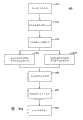
根据本发明的具体实施例,提供系统操作者数种处理半导体晶片的方法。例如,图9A为一流程图示,描绘方法900,其中沉积系统可根据本发明运作。首先,于步骤910,一晶片是藉由熟知此项技艺人士已知的装置,置入沉积室。于步骤912,密封沉积室并排空至一降低压力。于图9A所绘示的具体实施例,沉积室可藉由开启连接至主要泵,于前管线中的阀而排空。于其他具体实施例,沉积室可藉由开启连接至次要排气泵,或是连接至主要与次要泵组合,前管线中的阀而排空。于根据本发明的一些具体实施例,压力可下降至足以支援于沉积室内产生等离子体的程度。例如,压力可下降至介于5至20陶尔(torr)间。According to embodiments of the present invention, system operators are provided with several methods of processing semiconductor wafers. For example, FIG. 9A is a flow diagram depicting a
一旦沉积室到达所需压力,于步骤912,制程气体经由位于喷气头面板的数个孔隙,引入至沉积室。这些气体散流孔隙的数目,大小与分布,已于上详述。制程气体流经半导体晶片顶部表面,并与表面或其他气态物种反应,以于晶片表面形成所需薄膜。Once the deposition chamber reaches the desired pressure, at
制程气体与反应副产物同时由沉积室,经由步骤916的主要径向排气路径,以及步骤918中,于喷气头含有排气通道的次要排气路径排出。通过这些其他排气路径的气体体积比例,可藉由安装于个别路径上排气线路的阀的相对位置,加以控制。Process gases and reaction by-products are simultaneously exhausted from the deposition chamber through a primary radial exhaust path in
于完成沉积制程,于步骤920,停止传送制程气体。于步骤922与924,分别使沉积室返回至大气压力,并移除晶片。Upon completion of the deposition process, at
图9B为一流程图示,绘示根据本发明,操作沉积系统方法的另一具体实施例。于方法901的步骤930,一晶片是置入沉积室。于步骤932,使用主要排气路径,密封与排空沉积室至一降低压力。于图9B所绘示方法的另一具体实施例,沉积室是藉由开启位于连接至主要排气泵的前管线的阀而排空,一旦沉积室到达所需的压力,于步骤934,制程气体是经由位于喷气头面板的数个孔隙引入。于步骤936,经由使用主要排气通道,达成开始排出制程气体与反应副产物。随后,于步骤938,制程气体与反应副产物同时由沉积室,经由第一径向排气路径排出,且于步骤940,经由包含喷气头中排气通道的次要排气路径排出。于图9B所示的方法901的另一具体实施例,大多数排出气体通过主要排气通道,线路与泵。相较于主要排气路径,次要排气路径用于移除来自沉积室较少数量的气体,从而提供操作者对于制程参数的“微调”控制。通过次要与主要排气路径的气体体积比例,可于接近零与一的数值间变化。FIG. 9B is a flowchart illustrating another embodiment of a method of operating a deposition system according to the present invention. In
完成沉积制程后,于步骤942,停止制程气体的传送,于步骤944与946,分别使沉积室返回至大气压力,并移除晶片。After the deposition process is completed, at
图9C为根据本发明,操作沉积室方法的再另一具体实施例的流程图示。于方法902的步骤950,将晶片置入沉积室。于步骤952,排空沉积室,且于步骤954,使等离子体撞击沉积室。沉积室可经由主要或次要排气路径,或两者组合排出气体而排空。当等离子体稳定后,于步骤956,经由位于面板表面的数个孔隙,引入制程气体至沉积室。9C is a flowchart diagram of yet another embodiment of a method of operating a deposition chamber according to the present invention. At
制程气体与反应副产物由沉积室,于步骤958与960,分别经由主要与次要排气路径移除。于图9C所绘示方法902的具体实施例,于步骤962与964,于沉积制程中,调整主要与次要排气路径的排气速率。于一些具体实施例,于沉积过程中,可变化排气速率,以调变沉积薄膜的特性。这些特性可包含,但不限于,薄膜厚度,密度,折射是数,或电介质常数。Process gases and reaction byproducts are removed from the deposition chamber through primary and secondary exhaust paths, respectively, at
完成沉积制程后,于步骤966,停止制程气体的流动。于步骤968与970,分别使沉积室排空至大气压力,并移除晶片。After the deposition process is completed, at
经由根据本发明具体实施例的喷气头,所提供的补充排气路径,相较于习知技艺,提供某些优点。除了于基座边缘提供的传统排气路径(见图3A的流动线路322),于喷气头的排气孔隙,提供一补充排气路径,有用于最佳化接近晶片表面的反应种类流动。此外,为径向距离函数,散流相对于排气面积的比例变化性,对于制程气体与反应副产物的散流与排气,提供空间上的控制。The supplementary exhaust path provided via the injector head according to embodiments of the present invention offers certain advantages over the prior art. In addition to the traditional exhaust path provided at the edge of the susceptor (see
根据本发明一具体实施例,于径向方向流经晶片表面,并经由径向排气路径流出的气体体积,可藉由面板的设计而修改。于此一具体实施例,藉由制程气体与反应副产物,通过补充喷气头排气路径的选择性排出,可控制横向流经晶片表面的反应气态物种体积与浓度。于一特定具体实施例,流经晶片的反应气态物种体积与浓度,藉由增加横向流动体积区域的排气孔隙面积,可维持于为径向距离函数的一定值。此改进制程控制可产生较高的薄膜一致性。According to an embodiment of the present invention, the volume of gas flowing in the radial direction across the wafer surface and out through the radial exhaust paths can be modified by the design of the panel. In this embodiment, the volume and concentration of reactive gaseous species flowing laterally across the wafer surface can be controlled by supplementing the selective exhaust of the showerhead exhaust path with process gases and reaction by-products. In a specific embodiment, the volume and concentration of reactant gaseous species flowing through the wafer can be maintained at a constant value as a function of radial distance by increasing the vent pore area in the lateral flow volume region. This improved process control results in higher film uniformity.
于本发明其他具体实施例,反应种类于晶片表面的留置时间,可藉由喷气头排气孔隙面积的空间分布而控制。例如,图8显示根据本发明的一具体实施例,其中接近晶片中心835与边缘840,喷气头所提供的排气孔隙面积,小于距离等于1/2面板半径处的排气孔隙面积。于距离等于1/2面板半径的区域,可称为中间半径区域830。因此,于晶片中心835引入的制程气体,在经由中间半径区域830的面板,离开反应区域前,相较于靠近中间半径区域830引入的制程气体,于晶片表面行经较长的距离。于其他具体实施例,接近中间半径区域,通过晶片表面的制程气体流动,藉由气体散流与排气孔隙的选择性配置而增强。In other embodiments of the present invention, the residence time of the reactive species on the wafer surface can be controlled by the spatial distribution of the exhaust pore area of the nozzle. For example, FIG. 8 shows an embodiment in accordance with the present invention wherein near the center 835 and edge 840 of the wafer, the air showerhead provides a smaller vent area than at a distance equal to 1/2 the panel radius. The area where the distance is equal to 1/2 the radius of the panel may be referred to as the middle radius area 830 . Thus, process gas introduced at the center of the wafer 835 travels a longer distance across the wafer surface than process gases introduced near the middle radius region 830 before leaving the reaction region through the panel at the middle radius region 830 . In other embodiments, process gas flow across the wafer surface is enhanced near the mid-radius region by selective placement of gas diffusers and vent apertures.
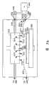
图1A是显示可实施本发明方法的一适当化学气相沉积设备,其为化学气相沉积系统10的一垂直截面图示,具有一真空或制程室15,包含制程室侧壁15a与制程室盖子组件15b。制程室侧壁15a与制程室盖子组件15b于图1B与1C图以分解透视图示显示。FIG. 1A is a diagram illustrating a suitable chemical vapor deposition apparatus that can be used to practice the method of the present invention. It is a vertical cross-sectional illustration of a chemical
化学气相沉积系统10含有一气体散流歧管11,以散布制程气体至一基材(未显示),是位于制程室中心的加热晶座12上。于制程时,基材,例如一半导体基材,位于晶座12的一平坦(或轻微凸面)表面12a(图1B)。晶座可于一下方载入/卸载位置(未显示),以及一上方制程位置(示于图1A)间控制移动,其是与歧管11紧邻。一活动平板(未显示),含有感应器,以提供晶片位置的资讯。The chemical
沉积与载体气体,是经由平坦,圆形气体散流面板13a的穿孔孔洞13b(图1C),引入制程室15,如上所详述。更具体地,沉积制程气体经由入口歧管11(由图1A的箭头40表示),经由一常见穿孔阻挡板42,且接着经由气体散流面板13a中的孔洞13b,流入制程室。Deposition and carrier gases are introduced into the
到达歧管前,沉积与载体气体由气体源7a,经由气体传送系统7的气体供应线路8,输入至一混合系统9,于此处结合并接着传送至歧管11。通常,每个制程气体的供应线路包含(i)数个安全关闭阀(未显示),用于自动或手动关闭制程气体流动进入制程室,及(ii)质流控制器(亦未显示),用以测量通过供应线路的气体流量。当毒性气体(例如臭氧或卤素气体)于制程中使用时,数个安全关闭阀以常见组态置于每个气体供应线路。Before reaching the manifold, the deposition and carrier gases are input from a gas source 7 a via a gas supply line 8 of a gas delivery system 7 to a mixing system 9 where they are combined and then delivered to a
于化学气相沉积系统14执行的沉积制程,可为一热制程或等离子体增强制程。于等离子体增强制程,一射频(RF)电源44于气体散流面板13a与晶座间施加电源,以激发制程气体混合物,以于面板13a与晶座间的圆柱区域,称为“反应区域”内形成等离子体。等离子体成分反应而沉积一所需的薄膜于由晶座12所支撑的半导体晶片表面。射频电源44为一混合频率无线电电源,典型地于13.56兆赫的高无线电频路(RF1),以及360千赫的低射频(RF2)供应电源,以增强引入真空室15的反应种类的分解。于热制程,将不利用射频电源44,且制程气体混合物热反应,以沉积所需的薄膜于由晶座12所支撑的半导体晶片表面,其对于加热具有阻抗,以提供反应所需的热能。The deposition process performed in the chemical
于等离子体增强沉积制程,等离子体加热整个制程室10,包含制程室本体的侧壁15a,围绕排气通道23与关闭阀24。当未开启等离子体或于热沉积制程时,一热液体于制程室的侧壁15a循环,以维持制程室于一升高温度。用于加热制程室侧壁15a的液体,包含典型液体类型,即,以水稀释的乙二醇或以油稀释的热转移液体。此类加热有利地减少或消除反应产物不希望的冷凝,并改进消除制程气体的挥发性产物,以及可能污染制程的其他污染物,若其于冷却的真空通道侧壁冷凝,并于无气体流动时期,回流至制程室。During the plasma enhanced deposition process, the plasma heats the
未沉积的剩余气体混合物,包含反应产物,是由制程室藉由连接至排气通道23的真空泵50,由前管线55排出。具体地,气体经由环绕反应区域的一环状,狭缝形孔隙16排出,并进入一环状排气空间17。环状狭缝16与空间17,是由制程室顶部的圆柱状侧壁15a(包含侧壁的上层电介质内层19),以及环状制程室盖子120底部间的缺口所定义。狭缝孔隙16与空间17的360度环状对称与一致性,对于达到晶片表面制程气体的一致性流动,以于晶片沉积一致性薄膜,一般而言为重要的。The undeposited remaining gas mixture, including the reaction products, is exhausted from the process chamber through the
由排气空间17,气体流经排气空间17侧边延伸部分21下方,通过一观察通道(未显示),经由一向下延伸的气体通道23,通过真空关闭阀24(其本体与下方制程室侧壁15a结合),并进入经由前管线55,连接至外部真空泵50的排气出口25。From the exhaust space 17, the gas flows through the
晶座12的晶片支撑转盘(较佳地为铝、陶瓷、或其组合)为抗加热,使用一嵌入式单一回圈嵌入加热器元件,装配为平行同心圆形式的两个完整弯曲。加热器元件外围部分,沿支撑转盘周围行进,且内部部分沿较小半径的同心圆路径行进。加热器元件的线路通过晶座12的柄。The wafer support turntable of susceptor 12 (preferably aluminum, ceramic, or a combination thereof) is heat resistant, using an embedded single loop embedded in the heater element, assembled as two complete bends in the form of parallel concentric circles. The outer portion of the heater element travels around the support turntable and the inner portion follows a smaller radius concentric circular path. The wiring of the heater element passes through the stem of the
典型地,任何或所有制程室内层、气体入口歧管面板,与各种其他反应器硬体,是由例如铝、电镀铝、或陶瓷材料所制成。此类化学气相沉积设备的一范例,是于美国专利第5,558,717号,发明名称「CVD ProcessingChamber」中描述。美国专利第5,558,717号的专利权属于应用材料公司,是为本发明的专利权人,于此并入参考。Typically, any or all of the process chamber layers, gas inlet manifold panels, and various other reactor hardware are fabricated from materials such as aluminum, anodized aluminum, or ceramics. An example of such a chemical vapor deposition apparatus is described in US Patent No. 5,558,717, titled "CVD Processing Chamber". US Patent No. 5,558,717 belongs to Applied Materials, Inc., the assignee of the present invention, and is hereby incorporated by reference.
一提升机构与马达(未显示),升高与降低加热晶座组件12与其晶片提升接脚12b,当晶片藉由一机械刀片(未显示),通过制程室10侧的一插入/移除开口26,移入或移出制程室本体时。马达于一制程位置14与一较低晶片载入位置间,升高与降低晶座12。马达、连接至供应线路8的阀或流体控制器、气体传送系统、节流阀、射频电源44,以及制程室与基座加热系统,均由系统控制器34(图1A),经由控制线路36所控制,其中仅显示一部份。控制器34根据来自光学感应器的反馈,决定可移动机械组件的位置,例如节流阀与晶座,其藉由控制器34控制下的适当马达所移动。A lift mechanism and motor (not shown) to raise and lower the
于一具体实施例,系统控制器包含一硬盘(存储器38)、一软盘与一处理器37。制程器含有一单一主机板电脑(Single-Board Computer,SBC),类比与数位输入/输出主机板、介面主机板与步径马达控制器主机板。化学气相沉积系统10的各个部分,是符合VME(Versa Modular European)标准,其定义主机板,介面卡与连接器大小与类型。VME标准亦定义总线结构,具有16位元数据总线与24位元位址总线。In one embodiment, the system controller includes a hard disk (memory 38 ), a floppy disk and a
系统控制器34控制化学气相沉积机器的所有活动。系统控制器执行系统控制软件,其为一电脑程式,储存于一电脑可读取媒体,例如存储器38。较佳地,存储器38为硬盘,但存储器38亦可为其他种类的存储器。电脑程式包含一组指令,指定引入与排出气体的时间、气体混合、制程室压力、制程室温度、射频电源程度、晶座位置、以及特定制程的其他参数。储存于其他存储器装置,包含,例如软盘或其他适当磁碟的其他电脑程式,亦可用于操作控制器34。A
上述反应器描述主要用于说明目的,且可利用其他等离子体化学气相沉积设备,例如电子回旋共振(ECR)等离子体化学气相沉积装置、感应耦合射频高密度等离子体化学气相沉积装置等。此外,上述系统的变化,例如晶座设计、加热器设计、射频电源频率、射频电源连接位置与其他的变化等亦为可能的。例如,晶片可由晶座所支撑,并由石英灯加热。本发明的层,以及形成此层的方法,并未限于任何特定设备或任何特定等离子体激发方法。The above reactor description is mainly for illustration purposes, and other plasma chemical vapor deposition equipment can be utilized, such as electron cyclotron resonance (ECR) plasma chemical vapor deposition equipment, inductively coupled radio frequency high density plasma chemical vapor deposition equipment, and the like. In addition, variations of the above systems, such as susceptor design, heater design, RF power frequency, RF power connection location, and other variations are also possible. For example, a wafer may be supported by a susceptor and heated by a quartz lamp. The layers of the present invention, and the method of forming such layers, are not limited to any particular apparatus or to any particular method of plasma excitation.
需了解此处所述的发明,可用于使用喷气头,以分布制程气体至基材的任何基板制程系统。此包含化学气相沉积、氮化、氧化、蚀刻与清理系统,仅列出数个范例。虽然此处已详细显示与描述包含本发明教示的各种具体实施例,熟知此项技艺的人士亦可轻易地设计仍含有这些教示的许多其他变化具体实施例。It will be appreciated that the invention described herein may be used in any substrate processing system that uses a gas showerhead to distribute process gases to a substrate. This includes chemical vapor deposition, nitridation, oxidation, etch and cleaning systems, just to name a few. While various embodiments incorporating the teachings of the present invention have been shown and described in detail herein, those skilled in the art can readily design many other varied embodiments that still incorporate these teachings.
其他具体实施例是于权利要求范围中。Other specific embodiments are within the scope of the following claims.
Claims (22)
Applications Claiming Priority (3)
| Application Number | Priority Date | Filing Date | Title |
|---|---|---|---|
| US10/717,881US20050103265A1 (en) | 2003-11-19 | 2003-11-19 | Gas distribution showerhead featuring exhaust apertures |
| US10/717,881 | 2003-11-19 | ||
| PCT/US2004/039065WO2005052998A2 (en) | 2003-11-19 | 2004-11-19 | Gas distribution showerhead featuring exhaust apertures |
Publications (2)
| Publication Number | Publication Date |
|---|---|
| CN101120122A CN101120122A (en) | 2008-02-06 |
| CN101120122Btrue CN101120122B (en) | 2011-02-16 |
Family
ID=34574628
Family Applications (1)
| Application Number | Title | Priority Date | Filing Date |
|---|---|---|---|
| CN2004800339871AExpired - Fee RelatedCN101120122B (en) | 2003-11-19 | 2004-11-19 | Gas distribution showerhead featuring exhaust apertures |
Country Status (6)
| Country | Link |
|---|---|
| US (2) | US20050103265A1 (en) |
| JP (1) | JP5001656B2 (en) |
| KR (1) | KR101081628B1 (en) |
| CN (1) | CN101120122B (en) |
| TW (1) | TWI332997B (en) |
| WO (1) | WO2005052998A2 (en) |
Families Citing this family (87)
| Publication number | Priority date | Publication date | Assignee | Title |
|---|---|---|---|---|
| US20050103265A1 (en)* | 2003-11-19 | 2005-05-19 | Applied Materials, Inc., A Delaware Corporation | Gas distribution showerhead featuring exhaust apertures |
| JP4790291B2 (en)* | 2005-03-10 | 2011-10-12 | 東京エレクトロン株式会社 | Substrate processing method, recording medium, and substrate processing apparatus |
| JPWO2007018139A1 (en)* | 2005-08-10 | 2009-02-19 | 株式会社日立国際電気 | Semiconductor device manufacturing method and substrate processing apparatus |
| US7718030B2 (en)* | 2005-09-23 | 2010-05-18 | Tokyo Electron Limited | Method and system for controlling radical distribution |
| US20070095283A1 (en)* | 2005-10-31 | 2007-05-03 | Galewski Carl J | Pumping System for Atomic Layer Deposition |
| US7645483B2 (en)* | 2006-01-17 | 2010-01-12 | Eastman Kodak Company | Two-dimensional aperture array for vapor deposition |
| JP4782585B2 (en)* | 2006-02-28 | 2011-09-28 | 株式会社日立ハイテクノロジーズ | Plasma etching apparatus and method |
| US7670432B2 (en)* | 2006-03-08 | 2010-03-02 | Tokyo Electron Limited | Exhaust system for a vacuum processing system |
| US7794546B2 (en)* | 2006-03-08 | 2010-09-14 | Tokyo Electron Limited | Sealing device and method for a processing system |
| JP5179739B2 (en)* | 2006-09-27 | 2013-04-10 | 東京エレクトロン株式会社 | Vapor deposition apparatus, vapor deposition apparatus control apparatus, vapor deposition apparatus control method, and vapor deposition apparatus usage method |
| US7879401B2 (en)* | 2006-12-22 | 2011-02-01 | The Regents Of The University Of Michigan | Organic vapor jet deposition using an exhaust |
| US20080166880A1 (en)* | 2007-01-08 | 2008-07-10 | Levy David H | Delivery device for deposition |
| US7789961B2 (en)* | 2007-01-08 | 2010-09-07 | Eastman Kodak Company | Delivery device comprising gas diffuser for thin film deposition |
| WO2008129977A1 (en)* | 2007-04-17 | 2008-10-30 | Ulvac, Inc. | Film forming apparatus |
| JP4900956B2 (en)* | 2007-06-25 | 2012-03-21 | 東京エレクトロン株式会社 | Gas supply mechanism and substrate processing apparatus |
| US8528498B2 (en)* | 2007-06-29 | 2013-09-10 | Lam Research Corporation | Integrated steerability array arrangement for minimizing non-uniformity |
| US9105449B2 (en)* | 2007-06-29 | 2015-08-11 | Lam Research Corporation | Distributed power arrangements for localizing power delivery |
| KR100888652B1 (en)* | 2007-08-14 | 2009-03-13 | 세메스 주식회사 | Exhaust plasma generator and atmospheric pressure plasma apparatus having the same |
| US8395250B2 (en)* | 2007-09-04 | 2013-03-12 | Kabushiki Kaisha Sharp | Plasma processing apparatus with an exhaust port above the substrate |
| US8398770B2 (en)* | 2007-09-26 | 2013-03-19 | Eastman Kodak Company | Deposition system for thin film formation |
| US8211231B2 (en)* | 2007-09-26 | 2012-07-03 | Eastman Kodak Company | Delivery device for deposition |
| JP4956470B2 (en)* | 2007-11-29 | 2012-06-20 | 株式会社ニューフレアテクノロジー | Semiconductor manufacturing apparatus and semiconductor manufacturing method |
| US7967912B2 (en)* | 2007-11-29 | 2011-06-28 | Nuflare Technology, Inc. | Manufacturing apparatus for semiconductor device and manufacturing method for semiconductor device |
| US8512509B2 (en)* | 2007-12-19 | 2013-08-20 | Applied Materials, Inc. | Plasma reactor gas distribution plate with radially distributed path splitting manifold |
| US8010225B2 (en)* | 2008-01-30 | 2011-08-30 | International Business Machines Corporation | Method and system of monitoring manufacturing equipment |
| JP5202050B2 (en)* | 2008-03-14 | 2013-06-05 | 東京エレクトロン株式会社 | Shower head and substrate processing apparatus |
| JP5179389B2 (en) | 2008-03-19 | 2013-04-10 | 東京エレクトロン株式会社 | Shower head and substrate processing apparatus |
| JP4731580B2 (en)* | 2008-03-27 | 2011-07-27 | 東京エレクトロン株式会社 | Film forming method and film forming apparatus |
| JP5231117B2 (en)* | 2008-07-24 | 2013-07-10 | 株式会社ニューフレアテクノロジー | Film forming apparatus and film forming method |
| KR101470883B1 (en)* | 2008-12-29 | 2014-12-10 | 주식회사 케이씨텍 | Atomic layer deposition apparatus |
| JP5221421B2 (en)* | 2009-03-10 | 2013-06-26 | 東京エレクトロン株式会社 | Shower head and plasma processing apparatus |
| JP5323628B2 (en)* | 2009-09-17 | 2013-10-23 | 東京エレクトロン株式会社 | Plasma processing equipment |
| JP5367522B2 (en) | 2009-09-24 | 2013-12-11 | 東京エレクトロン株式会社 | Plasma processing apparatus and shower head |
| JP5432686B2 (en)* | 2009-12-03 | 2014-03-05 | 東京エレクトロン株式会社 | Plasma processing equipment |
| US9111729B2 (en) | 2009-12-03 | 2015-08-18 | Lam Research Corporation | Small plasma chamber systems and methods |
| JP2011144412A (en)* | 2010-01-13 | 2011-07-28 | Honda Motor Co Ltd | Plasma film-forming apparatus |
| FI124414B (en)* | 2010-04-30 | 2014-08-29 | Beneq Oy | Outlets and apparatus for processing substrates |
| JP5591585B2 (en)* | 2010-05-17 | 2014-09-17 | 東京エレクトロン株式会社 | Plasma processing equipment |
| US9184028B2 (en) | 2010-08-04 | 2015-11-10 | Lam Research Corporation | Dual plasma volume processing apparatus for neutral/ion flux control |
| JP5625598B2 (en)* | 2010-08-04 | 2014-11-19 | アイシン精機株式会社 | Carbon nanotube device |
| JP5630640B2 (en)* | 2010-08-04 | 2014-11-26 | アイシン精機株式会社 | Carbon nanotube manufacturing method and carbon nanotube manufacturing apparatus |
| US20130059448A1 (en)* | 2011-09-07 | 2013-03-07 | Lam Research Corporation | Pulsed Plasma Chamber in Dual Chamber Configuration |
| CN103052593B (en)* | 2010-08-04 | 2015-04-29 | 爱信精机株式会社 | Carbon nanotube equipment, carbon nanotube manufacturing method, and carbon nanotube manufacturing device |
| US8869742B2 (en)* | 2010-08-04 | 2014-10-28 | Lam Research Corporation | Plasma processing chamber with dual axial gas injection and exhaust |
| US9967965B2 (en) | 2010-08-06 | 2018-05-08 | Lam Research Corporation | Distributed, concentric multi-zone plasma source systems, methods and apparatus |
| US9449793B2 (en) | 2010-08-06 | 2016-09-20 | Lam Research Corporation | Systems, methods and apparatus for choked flow element extraction |
| EP2504536B1 (en)* | 2010-08-06 | 2019-03-13 | AVL Test Systems, Inc. | Particulate measurement system |
| US8580044B2 (en)* | 2010-08-13 | 2013-11-12 | Samsung Austin Semiconductor, L.P. | Apparatus for agitating and evacuating byproduct dust from a semiconductor processing chamber |
| TWI507561B (en)* | 2010-12-10 | 2015-11-11 | Ind Tech Res Inst | Showerhead integrating intake and exhaust |
| GB201021870D0 (en)* | 2010-12-23 | 2011-02-02 | Element Six Ltd | A microwave plasma reactor for manufacturing synthetic diamond material |
| US8597429B2 (en) | 2011-01-18 | 2013-12-03 | Nuflare Technology, Inc. | Manufacturing apparatus and method for semiconductor device |
| US20130034666A1 (en)* | 2011-08-01 | 2013-02-07 | Applied Materials, Inc. | Inductive plasma sources for wafer processing and chamber cleaning |
| US9175393B1 (en)* | 2011-08-31 | 2015-11-03 | Alta Devices, Inc. | Tiled showerhead for a semiconductor chemical vapor deposition reactor |
| US10066297B2 (en)* | 2011-08-31 | 2018-09-04 | Alta Devices, Inc. | Tiled showerhead for a semiconductor chemical vapor deposition reactor |
| US10283325B2 (en) | 2012-10-10 | 2019-05-07 | Lam Research Corporation | Distributed multi-zone plasma source systems, methods and apparatus |
| US8900364B2 (en)* | 2011-11-29 | 2014-12-02 | Intermolecular, Inc. | High productivity vapor processing system |
| US9982340B2 (en)* | 2012-04-04 | 2018-05-29 | Taiwan Semiconductor Manufacturing Co. Ltd. | Shower head apparatus and method for controlling plasma or gas distribution |
| US9982343B2 (en)* | 2012-12-14 | 2018-05-29 | Applied Materials, Inc. | Apparatus for providing plasma to a process chamber |
| JP6119408B2 (en)* | 2013-05-09 | 2017-04-26 | ソニー株式会社 | Atomic layer deposition equipment |
| JP5793170B2 (en)* | 2013-09-30 | 2015-10-14 | 株式会社日立国際電気 | Semiconductor device manufacturing method, substrate processing apparatus, and program |
| JP5800952B1 (en)* | 2014-04-24 | 2015-10-28 | 株式会社日立国際電気 | Substrate processing apparatus, semiconductor device manufacturing method, program, and recording medium |
| US9228260B1 (en)* | 2014-07-30 | 2016-01-05 | Taiwan Semiconductor Manufacturing Co., Ltd. | Wafer processing chamber, heat treatment apparatus and method for processing wafers |
| CN104213102B (en)* | 2014-09-01 | 2016-08-24 | 沈阳拓荆科技有限公司 | Cavity airflow direction varistructure |
| JP6327189B2 (en)* | 2015-04-03 | 2018-05-23 | 株式会社島津製作所 | Process processing equipment |
| KR102420015B1 (en)* | 2015-08-28 | 2022-07-12 | 삼성전자주식회사 | Shower head of Combinatorial Spatial Atomic Layer Deposition apparatus |
| US10453721B2 (en) | 2016-03-15 | 2019-10-22 | Applied Materials, Inc. | Methods and assemblies for gas flow ratio control |
| US10269600B2 (en) | 2016-03-15 | 2019-04-23 | Applied Materials, Inc. | Methods and assemblies for gas flow ratio control |
| USD794753S1 (en) | 2016-04-08 | 2017-08-15 | Applied Materials, Inc. | Showerhead for a semiconductor processing chamber |
| USD793526S1 (en) | 2016-04-08 | 2017-08-01 | Applied Materials, Inc. | Showerhead for a semiconductor processing chamber |
| USD790039S1 (en) | 2016-04-08 | 2017-06-20 | Applied Materials, Inc. | Showerhead for a semiconductor processing chamber |
| JP6814561B2 (en)* | 2016-07-07 | 2021-01-20 | 昭和電工株式会社 | Gas piping system, chemical vapor deposition equipment, film formation method and method for manufacturing SiC epitaxial wafer |
| US10403476B2 (en) | 2016-11-09 | 2019-09-03 | Lam Research Corporation | Active showerhead |
| KR102410571B1 (en) | 2016-12-09 | 2022-06-22 | 에이에스엠 아이피 홀딩 비.브이. | Thermal Atomic Layer Etching Processes |
| US10801106B2 (en)* | 2016-12-15 | 2020-10-13 | Asm Ip Holding B.V. | Shower plate structure for exhausting deposition inhibiting gas |
| US10283319B2 (en) | 2016-12-22 | 2019-05-07 | Asm Ip Holding B.V. | Atomic layer etching processes |
| KR102493945B1 (en)* | 2017-06-06 | 2023-01-30 | 어플라이드 머티어리얼스, 인코포레이티드 | Deposition radial and edge profile tenability through independent control of teos flow |
| KR101939481B1 (en)* | 2017-07-27 | 2019-01-16 | 성균관대학교산학협력단 | Ion bean etching apparatus |
| US11047050B2 (en) | 2018-10-30 | 2021-06-29 | Taiwan Semiconductor Manufacturing Co., Ltd. | Semiconductor tool having controllable ambient environment processing zones |
| WO2020163074A1 (en)* | 2019-02-05 | 2020-08-13 | Applied Materials, Inc. | Multi channel splitter spool |
| KR102204883B1 (en) | 2019-05-09 | 2021-01-19 | 세메스 주식회사 | Apparatus for treating substrate |
| JP7737789B2 (en)* | 2019-07-18 | 2025-09-11 | エーエスエム・アイピー・ホールディング・ベー・フェー | Showerhead device for semiconductor processing system |
| US11574813B2 (en) | 2019-12-10 | 2023-02-07 | Asm Ip Holding B.V. | Atomic layer etching |
| US11854839B2 (en) | 2020-04-15 | 2023-12-26 | Mks Instruments, Inc. | Valve apparatuses and related methods for reactive process gas isolation and facilitating purge during isolation |
| US20210404059A1 (en)* | 2020-06-26 | 2021-12-30 | Applied Materials, Inc. | Processing system and method of controlling conductance in a processing system |
| CN112522682B (en)* | 2020-11-03 | 2022-05-27 | 鑫天虹(厦门)科技有限公司 | Atomic layer deposition apparatus and process |
| CN113471123B (en)* | 2021-07-06 | 2023-08-25 | 华海清科股份有限公司 | Wafer vertical rotation processing equipment and ventilation system applied by same |
| CN118996617B (en)* | 2024-10-22 | 2025-01-24 | 江苏岚玥新材料科技有限公司 | A gas supply device for silicon carbide epitaxial chemical vapor deposition system |
Citations (2)
| Publication number | Priority date | Publication date | Assignee | Title |
|---|---|---|---|---|
| US5422139A (en)* | 1990-04-12 | 1995-06-06 | Balzers Aktiengesellschaft | Method for a reactive surface treatment of a workpiece and a treatment chamber for practicing such method |
| CN1213848A (en)* | 1997-09-19 | 1999-04-14 | 西门子公司 | Spatially uniform gas supply and pump configuration for large wafer diameters |
Family Cites Families (35)
| Publication number | Priority date | Publication date | Assignee | Title |
|---|---|---|---|---|
| US4209357A (en)* | 1979-05-18 | 1980-06-24 | Tegal Corporation | Plasma reactor apparatus |
| US4579618A (en)* | 1984-01-06 | 1986-04-01 | Tegal Corporation | Plasma reactor apparatus |
| US4590042A (en)* | 1984-12-24 | 1986-05-20 | Tegal Corporation | Plasma reactor having slotted manifold |
| JPS61174388A (en)* | 1985-01-30 | 1986-08-06 | Hitachi Ltd | Etching device |
| US4793975A (en)* | 1985-05-20 | 1988-12-27 | Tegal Corporation | Plasma Reactor with removable insert |
| JPH01108930U (en)* | 1988-01-14 | 1989-07-24 | ||
| KR0170391B1 (en)* | 1989-06-16 | 1999-03-30 | 다카시마 히로시 | Object processing device and processing method |
| US4993358A (en)* | 1989-07-28 | 1991-02-19 | Watkins-Johnson Company | Chemical vapor deposition reactor and method of operation |
| US5427625A (en)* | 1992-12-18 | 1995-06-27 | Tokyo Electron Kabushiki Kaisha | Method for cleaning heat treatment processing apparatus |
| US5614055A (en)* | 1993-08-27 | 1997-03-25 | Applied Materials, Inc. | High density plasma CVD and etching reactor |
| US5614026A (en)* | 1996-03-29 | 1997-03-25 | Lam Research Corporation | Showerhead for uniform distribution of process gas |
| JP3535309B2 (en)* | 1996-04-10 | 2004-06-07 | 東京エレクトロン株式会社 | Decompression processing equipment |
| US5976261A (en)* | 1996-07-11 | 1999-11-02 | Cvc Products, Inc. | Multi-zone gas injection apparatus and method for microelectronics manufacturing equipment |
| US6090210A (en)* | 1996-07-24 | 2000-07-18 | Applied Materials, Inc. | Multi-zone gas flow control in a process chamber |
| US5781693A (en)* | 1996-07-24 | 1998-07-14 | Applied Materials, Inc. | Gas introduction showerhead for an RTP chamber with upper and lower transparent plates and gas flow therebetween |
| US5789028A (en)* | 1997-03-04 | 1998-08-04 | Lsi Logic Corporation | Method for eliminating peeling at end of semiconductor substrate in metal organic chemical vapor deposition of titanium nitride |
| US6050506A (en)* | 1998-02-13 | 2000-04-18 | Applied Materials, Inc. | Pattern of apertures in a showerhead for chemical vapor deposition |
| JP2002511529A (en)* | 1998-04-14 | 2002-04-16 | シーブイデイ・システムズ・インコーポレーテツド | Thin film deposition system |
| US6086677A (en)* | 1998-06-16 | 2000-07-11 | Applied Materials, Inc. | Dual gas faceplate for a showerhead in a semiconductor wafer processing system |
| US6190732B1 (en)* | 1998-09-03 | 2001-02-20 | Cvc Products, Inc. | Method and system for dispensing process gas for fabricating a device on a substrate |
| KR100733237B1 (en)* | 1999-10-13 | 2007-06-27 | 동경 엘렉트론 주식회사 | Processing apparatus |
| US6444040B1 (en)* | 2000-05-05 | 2002-09-03 | Applied Materials Inc. | Gas distribution plate |
| AU2001288225A1 (en)* | 2000-07-24 | 2002-02-05 | The University Of Maryland College Park | Spatially programmable microelectronics process equipment using segmented gas injection showerhead with exhaust gas recirculation |
| JP2002100623A (en)* | 2000-09-20 | 2002-04-05 | Fuji Daiichi Seisakusho:Kk | Thin film semiconductor manufacturing apparatus |
| JP2002184764A (en)* | 2000-12-18 | 2002-06-28 | Hitachi Ltd | Plasma processing equipment |
| US6852167B2 (en)* | 2001-03-01 | 2005-02-08 | Micron Technology, Inc. | Methods, systems, and apparatus for uniform chemical-vapor depositions |
| WO2003062490A2 (en)* | 2002-01-17 | 2003-07-31 | Sundew Technologies, Llc | Ald apparatus and method |
| JP2004035971A (en)* | 2002-07-05 | 2004-02-05 | Ulvac Japan Ltd | Thin film manufacturing apparatus |
| US6821563B2 (en)* | 2002-10-02 | 2004-11-23 | Applied Materials, Inc. | Gas distribution system for cyclical layer deposition |
| US7270713B2 (en)* | 2003-01-07 | 2007-09-18 | Applied Materials, Inc. | Tunable gas distribution plate assembly |
| US6942753B2 (en)* | 2003-04-16 | 2005-09-13 | Applied Materials, Inc. | Gas distribution plate assembly for large area plasma enhanced chemical vapor deposition |
| US7601223B2 (en)* | 2003-04-29 | 2009-10-13 | Asm International N.V. | Showerhead assembly and ALD methods |
| US7408225B2 (en)* | 2003-10-09 | 2008-08-05 | Asm Japan K.K. | Apparatus and method for forming thin film using upstream and downstream exhaust mechanisms |
| US20050103265A1 (en) | 2003-11-19 | 2005-05-19 | Applied Materials, Inc., A Delaware Corporation | Gas distribution showerhead featuring exhaust apertures |
| US7273526B2 (en)* | 2004-04-15 | 2007-09-25 | Asm Japan K.K. | Thin-film deposition apparatus |
- 2003
- 2003-11-19USUS10/717,881patent/US20050103265A1/ennot_activeAbandoned
- 2004
- 2004-11-19CNCN2004800339871Apatent/CN101120122B/ennot_activeExpired - Fee Related
- 2004-11-19WOPCT/US2004/039065patent/WO2005052998A2/enactiveSearch and Examination
- 2004-11-19TWTW093135727Apatent/TWI332997B/ennot_activeIP Right Cessation
- 2004-11-19JPJP2006541584Apatent/JP5001656B2/ennot_activeExpired - Fee Related
- 2006
- 2006-06-13USUS11/452,786patent/US7452827B2/ennot_activeExpired - Fee Related
- 2006-06-19KRKR1020067012156Apatent/KR101081628B1/ennot_activeExpired - Fee Related
Patent Citations (2)
| Publication number | Priority date | Publication date | Assignee | Title |
|---|---|---|---|---|
| US5422139A (en)* | 1990-04-12 | 1995-06-06 | Balzers Aktiengesellschaft | Method for a reactive surface treatment of a workpiece and a treatment chamber for practicing such method |
| CN1213848A (en)* | 1997-09-19 | 1999-04-14 | 西门子公司 | Spatially uniform gas supply and pump configuration for large wafer diameters |
Also Published As
| Publication number | Publication date |
|---|---|
| US7452827B2 (en) | 2008-11-18 |
| US20060234514A1 (en) | 2006-10-19 |
| WO2005052998A3 (en) | 2007-11-01 |
| CN101120122A (en) | 2008-02-06 |
| WO2005052998A2 (en) | 2005-06-09 |
| JP2007525021A (en) | 2007-08-30 |
| TWI332997B (en) | 2010-11-11 |
| US20050103265A1 (en) | 2005-05-19 |
| TW200526799A (en) | 2005-08-16 |
| KR20060096460A (en) | 2006-09-11 |
| JP5001656B2 (en) | 2012-08-15 |
| WO2005052998A9 (en) | 2009-05-07 |
| KR101081628B1 (en) | 2011-11-09 |
Similar Documents
| Publication | Publication Date | Title |
|---|---|---|
| CN101120122B (en) | Gas distribution showerhead featuring exhaust apertures | |
| US5895530A (en) | Method and apparatus for directing fluid through a semiconductor processing chamber | |
| CN104250728B (en) | Chemical deposition chamber with gas seal | |
| US9267204B2 (en) | Film deposition apparatus, substrate processing apparatus, film deposition method, and storage medium | |
| US20070131169A1 (en) | Methods, systems, and apparatus for uniform chemical-vapor depositions | |
| US6818249B2 (en) | Reactors, systems with reaction chambers, and methods for depositing materials onto micro-device workpieces | |
| TWI721227B (en) | Film forming device and film forming method | |
| JP7401560B2 (en) | Heat treatment chamber lid with backside pumping | |
| JPH09181065A (en) | Deposition chamber | |
| KR20170007132A (en) | Substrate processing apparatus | |
| WO2006096674A1 (en) | Gas baffle and distributor for semiconductor processing chamber | |
| CN111378959B (en) | Film forming apparatus and film forming processing method | |
| JP2024511195A (en) | Hardware to prevent bottom purge intrusion into the application volume and handle gas diffusion below the heater | |
| JP2018110221A (en) | Chemical evaporation chamber for gas seal | |
| CN100466162C (en) | Edge Flow Panels for Improved CVD Film Performance | |
| TWI811817B (en) | Processing chamber deposition confinement | |
| CN108505020B (en) | Film forming apparatus | |
| JP2003253448A (en) | Substrate processing equipment | |
| CN119061379A (en) | Shower head, substrate processing device and substrate processing method | |
| CN119998494A (en) | Adjustable base | |
| CN119998493A (en) | Annular pumping for chambers | |
| CN117769754A (en) | Reactor with inductively coupled plasma source |
Legal Events
| Date | Code | Title | Description |
|---|---|---|---|
| C06 | Publication | ||
| PB01 | Publication | ||
| C10 | Entry into substantive examination | ||
| SE01 | Entry into force of request for substantive examination | ||
| C14 | Grant of patent or utility model | ||
| GR01 | Patent grant | ||
| C56 | Change in the name or address of the patentee | ||
| CP01 | Change in the name or title of a patent holder | Address after:American California Patentee after:Applied Materials Inc. Address before:American California Patentee before:Applied Materials Inc. | |
| CF01 | Termination of patent right due to non-payment of annual fee | Granted publication date:20110216 Termination date:20141119 | |
| EXPY | Termination of patent right or utility model |