CN101088109B - Combined EAS and RFID tag or label with controllable read range - Google Patents
Combined EAS and RFID tag or label with controllable read rangeDownload PDFInfo
- Publication number
- CN101088109B CN101088109BCN2005800447245ACN200580044724ACN101088109BCN 101088109 BCN101088109 BCN 101088109BCN 2005800447245 ACN2005800447245 ACN 2005800447245ACN 200580044724 ACN200580044724 ACN 200580044724ACN 101088109 BCN101088109 BCN 101088109B
- Authority
- CN
- China
- Prior art keywords
- rfid
- antenna
- eas
- tag
- rfid element
- Prior art date
- Legal status (The legal status is an assumption and is not a legal conclusion. Google has not performed a legal analysis and makes no representation as to the accuracy of the status listed.)
- Active
Links
Images


Classifications
- H—ELECTRICITY
- H01—ELECTRIC ELEMENTS
- H01Q—ANTENNAS, i.e. RADIO AERIALS
- H01Q1/00—Details of, or arrangements associated with, antennas
- H01Q1/12—Supports; Mounting means
- H01Q1/22—Supports; Mounting means by structural association with other equipment or articles
- H01Q1/2208—Supports; Mounting means by structural association with other equipment or articles associated with components used in interrogation type services, i.e. in systems for information exchange between an interrogator/reader and a tag/transponder, e.g. in Radio Frequency Identification [RFID] systems
- H01Q1/2216—Supports; Mounting means by structural association with other equipment or articles associated with components used in interrogation type services, i.e. in systems for information exchange between an interrogator/reader and a tag/transponder, e.g. in Radio Frequency Identification [RFID] systems used in interrogator/reader equipment
- G—PHYSICS
- G06—COMPUTING OR CALCULATING; COUNTING
- G06K—GRAPHICAL DATA READING; PRESENTATION OF DATA; RECORD CARRIERS; HANDLING RECORD CARRIERS
- G06K19/00—Record carriers for use with machines and with at least a part designed to carry digital markings
- G06K19/06—Record carriers for use with machines and with at least a part designed to carry digital markings characterised by the kind of the digital marking, e.g. shape, nature, code
- G06K19/067—Record carriers with conductive marks, printed circuits or semiconductor circuit elements, e.g. credit or identity cards also with resonating or responding marks without active components
- G06K19/07—Record carriers with conductive marks, printed circuits or semiconductor circuit elements, e.g. credit or identity cards also with resonating or responding marks without active components with integrated circuit chips
- G06K19/0723—Record carriers with conductive marks, printed circuits or semiconductor circuit elements, e.g. credit or identity cards also with resonating or responding marks without active components with integrated circuit chips the record carrier comprising an arrangement for non-contact communication, e.g. wireless communication circuits on transponder cards, non-contact smart cards or RFIDs
- G06K19/0726—Record carriers with conductive marks, printed circuits or semiconductor circuit elements, e.g. credit or identity cards also with resonating or responding marks without active components with integrated circuit chips the record carrier comprising an arrangement for non-contact communication, e.g. wireless communication circuits on transponder cards, non-contact smart cards or RFIDs the arrangement including a circuit for tuning the resonance frequency of an antenna on the record carrier
- G—PHYSICS
- G06—COMPUTING OR CALCULATING; COUNTING
- G06K—GRAPHICAL DATA READING; PRESENTATION OF DATA; RECORD CARRIERS; HANDLING RECORD CARRIERS
- G06K19/00—Record carriers for use with machines and with at least a part designed to carry digital markings
- G06K19/06—Record carriers for use with machines and with at least a part designed to carry digital markings characterised by the kind of the digital marking, e.g. shape, nature, code
- G06K19/067—Record carriers with conductive marks, printed circuits or semiconductor circuit elements, e.g. credit or identity cards also with resonating or responding marks without active components
- G06K19/07—Record carriers with conductive marks, printed circuits or semiconductor circuit elements, e.g. credit or identity cards also with resonating or responding marks without active components with integrated circuit chips
- G06K19/077—Constructional details, e.g. mounting of circuits in the carrier
- G06K19/07749—Constructional details, e.g. mounting of circuits in the carrier the record carrier being capable of non-contact communication, e.g. constructional details of the antenna of a non-contact smart card
- G—PHYSICS
- G08—SIGNALLING
- G08B—SIGNALLING OR CALLING SYSTEMS; ORDER TELEGRAPHS; ALARM SYSTEMS
- G08B13/00—Burglar, theft or intruder alarms
- G08B13/22—Electrical actuation
- G08B13/24—Electrical actuation by interference with electromagnetic field distribution
- G—PHYSICS
- G08—SIGNALLING
- G08B—SIGNALLING OR CALLING SYSTEMS; ORDER TELEGRAPHS; ALARM SYSTEMS
- G08B13/00—Burglar, theft or intruder alarms
- G08B13/22—Electrical actuation
- G08B13/24—Electrical actuation by interference with electromagnetic field distribution
- G08B13/2402—Electronic Article Surveillance [EAS], i.e. systems using tags for detecting removal of a tagged item from a secure area, e.g. tags for detecting shoplifting
- G08B13/2405—Electronic Article Surveillance [EAS], i.e. systems using tags for detecting removal of a tagged item from a secure area, e.g. tags for detecting shoplifting characterised by the tag technology used
- G08B13/2414—Electronic Article Surveillance [EAS], i.e. systems using tags for detecting removal of a tagged item from a secure area, e.g. tags for detecting shoplifting characterised by the tag technology used using inductive tags
- G08B13/2417—Electronic Article Surveillance [EAS], i.e. systems using tags for detecting removal of a tagged item from a secure area, e.g. tags for detecting shoplifting characterised by the tag technology used using inductive tags having a radio frequency identification chip
- G—PHYSICS
- G08—SIGNALLING
- G08B—SIGNALLING OR CALLING SYSTEMS; ORDER TELEGRAPHS; ALARM SYSTEMS
- G08B13/00—Burglar, theft or intruder alarms
- G08B13/22—Electrical actuation
- G08B13/24—Electrical actuation by interference with electromagnetic field distribution
- G08B13/2402—Electronic Article Surveillance [EAS], i.e. systems using tags for detecting removal of a tagged item from a secure area, e.g. tags for detecting shoplifting
- G08B13/2428—Tag details
- G08B13/2431—Tag circuit details
- G—PHYSICS
- G08—SIGNALLING
- G08B—SIGNALLING OR CALLING SYSTEMS; ORDER TELEGRAPHS; ALARM SYSTEMS
- G08B13/00—Burglar, theft or intruder alarms
- G08B13/22—Electrical actuation
- G08B13/24—Electrical actuation by interference with electromagnetic field distribution
- G08B13/2402—Electronic Article Surveillance [EAS], i.e. systems using tags for detecting removal of a tagged item from a secure area, e.g. tags for detecting shoplifting
- G08B13/2428—Tag details
- G08B13/2437—Tag layered structure, processes for making layered tags
- G—PHYSICS
- G08—SIGNALLING
- G08B—SIGNALLING OR CALLING SYSTEMS; ORDER TELEGRAPHS; ALARM SYSTEMS
- G08B13/00—Burglar, theft or intruder alarms
- G08B13/22—Electrical actuation
- G08B13/24—Electrical actuation by interference with electromagnetic field distribution
- G08B13/2402—Electronic Article Surveillance [EAS], i.e. systems using tags for detecting removal of a tagged item from a secure area, e.g. tags for detecting shoplifting
- G08B13/2428—Tag details
- G08B13/2448—Tag with at least dual detection means, e.g. combined inductive and ferromagnetic tags, dual frequencies within a single technology, tampering detection or signalling means on the tag
- H—ELECTRICITY
- H01—ELECTRIC ELEMENTS
- H01Q—ANTENNAS, i.e. RADIO AERIALS
- H01Q1/00—Details of, or arrangements associated with, antennas
- H01Q1/12—Supports; Mounting means
- H01Q1/22—Supports; Mounting means by structural association with other equipment or articles
- H01Q1/2208—Supports; Mounting means by structural association with other equipment or articles associated with components used in interrogation type services, i.e. in systems for information exchange between an interrogator/reader and a tag/transponder, e.g. in Radio Frequency Identification [RFID] systems
- H01Q1/2225—Supports; Mounting means by structural association with other equipment or articles associated with components used in interrogation type services, i.e. in systems for information exchange between an interrogator/reader and a tag/transponder, e.g. in Radio Frequency Identification [RFID] systems used in active tags, i.e. provided with its own power source or in passive tags, i.e. deriving power from RF signal
- H—ELECTRICITY
- H01—ELECTRIC ELEMENTS
- H01Q—ANTENNAS, i.e. RADIO AERIALS
- H01Q1/00—Details of, or arrangements associated with, antennas
- H01Q1/12—Supports; Mounting means
- H01Q1/22—Supports; Mounting means by structural association with other equipment or articles
- H01Q1/24—Supports; Mounting means by structural association with other equipment or articles with receiving set
Landscapes
- Physics & Mathematics (AREA)
- Engineering & Computer Science (AREA)
- General Physics & Mathematics (AREA)
- Electromagnetism (AREA)
- Automation & Control Theory (AREA)
- Computer Security & Cryptography (AREA)
- Theoretical Computer Science (AREA)
- Microelectronics & Electronic Packaging (AREA)
- Computer Hardware Design (AREA)
- Computer Networks & Wireless Communication (AREA)
- Burglar Alarm Systems (AREA)
- Details Of Aerials (AREA)
- Near-Field Transmission Systems (AREA)
Abstract
Description
Translated fromChinese相关申请的交叉引用Cross References to Related Applications
本申请根据35 U.S.C.§119要求2004年11月15日提交的美国临时专利申请No.60/628,303,名为“Combo EAS/RFID Label or Tag”的优先权,其整个内容在这里被并入以作参考。This application claims priority under 35 U.S.C. §119 to U.S. Provisional Patent Application No. 60/628,303, filed November 15, 2004, entitled "Combo EAS/RFID Label or Tag," the entire contents of which are incorporated herein as Reference.
技术领域technical field
本发明的公开内容涉及一种电子物品监视(EAS,electronicarticle surveillance)标志或标签,用于防止或制止从被控制区域未经授权地取走物品。更具体地说,本发明的公开内容涉及一种与射频识别(RFID)标志或标签结合起来的EAS标志或标签,用于记录所述物品特有的数据,以及一种新颖的RFID标志或标签。The disclosure of the present invention relates to an electronic article surveillance (EAS, electronic article surveillance) sign or label, which is used to prevent or stop unauthorized removal of articles from controlled areas. More specifically, the present disclosure relates to an EAS tag or tag combined with a Radio Frequency Identification (RFID) tag or tag for recording data specific to said item, and a novel RFID tag or tag.
背景技术Background technique
电子物品监视(EAS)系统在防止或制止从被控制区域未经授权地取走物品的技术领域中是已知的。在典型的EAS系统中,EAS标记(标签或标志)被设计来与位于被控制区域的出口处的电磁场交互作用。这些EAS标记被贴在要保护的物品上。如果EAS标签被带入到电磁场或“询问区”中,标签的存在被检测出来并采取适当的行动,如生成警报。对于经过授权地取走物品,EAS标签可以被禁用(deactivate)、取下或在该电磁场周围经过,以避免EAS系统的检测。Electronic Article Surveillance (EAS) systems are known in the art to prevent or deter unauthorized removal of items from controlled areas. In a typical EAS system, EAS markers (tags or signs) are designed to interact with electromagnetic fields located at exits from controlled areas. These EAS marks are affixed to the item to be protected. If an EAS tag is brought into an electromagnetic field or "interrogation zone," the presence of the tag is detected and appropriate action is taken, such as generating an alarm. For authorized removal of the item, the EAS tag can be deactivated, removed or passed around the electromagnetic field to avoid detection by the EAS system.
EAS系统典型地采用可重复使用的EAS标签或者一次性标签或标志来监控物品,以防止入店行窃以及从商店未经授权地拿走物品。可重复使用的EAS标签通常在顾客离开商店之前从物品上取下。一次性标签或标志通常用粘胶粘贴在包装上或被放置在包装内。这些标签典型地与物品在一起,并且必须在由用户从商店取走之前使其被禁用。禁用设备可以使用线圈,线圈被施加能量后可以产生足够大小的磁场以使得EAS标签无效。被禁用的标签不再对EAS系统的入射能量做出响应,从而不会触发警报。EAS systems typically employ reusable EAS tags or single-use tags or tags to monitor items to prevent shoplifting and unauthorized removal of items from stores. Reusable EAS tags are usually removed from items before customers leave the store. Disposable labels or signs are usually glued to the package or placed inside the package. These tags are typically with the item and must be disabled before being removed from the store by the user. A disabling device may use a coil that is energized to generate a magnetic field of sufficient magnitude to render the EAS tag ineffective. A disabled tag no longer responds to incident energy from the EAS system, thereby not triggering an alarm.
对于具有EAS标签的物品将被登记或被返回到被控制区域的情形,EAS标签必须被激活或被重新贴上以再次提供防窃功能。由于希望做出源标记,其中EAS标签在被制造或配送时被附加到物品上,典型地,EAS标签最好可以被禁用或激活,而不是从物品上取下。另外,物品在询问区周围经过时会产生其他问题,因为EAS标签仍保持有效,并可以与其他受控区域中的EAS系统进行交互,从而无意中激活那些系统。In the event that an item with an EAS tag is to be checked in or returned to a controlled area, the EAS tag must be activated or reapplied to again provide theft prevention. Since it is desirable to make source marking where an EAS tag is affixed to an item as it is being manufactured or distributed, it is typically preferred that the EAS tag be deactivated or activated rather than removed from the item. Additionally, items can create additional problems as they pass around the interrogation zone, since the EAS tags remain active and can interact with EAS systems in other controlled areas, activating those systems inadvertently.
射频识别(RFID)系统也是本领域中众所周知的,并且可用于若干应用,如管理存货(inventory)、电子访问控制、安全系统,以及收费公路上的车辆自动识别。RFID系统典型地包括RFID读取器和RFID设备。RFID读取器可以发送射频载波信号到RFID设备。RFID设备可以用数据信号来响应该载波信号,所述数据信号用RFID设备所存储的信息来编码。Radio Frequency Identification (RFID) systems are also well known in the art and are used in several applications such as managing inventory, electronic access control, security systems, and automatic vehicle identification on toll roads. RFID systems typically include RFID readers and RFID devices. RFID readers can send radio frequency carrier signals to RFID devices. The RFID device may respond to the carrier signal with a data signal encoded with information stored by the RFID device.
在零售环境中,组合了EAS和RFID功能的市场需求正快速兴起。很多零售商店目前用EAS防止入店行窃,它们依靠条形码信息进行存货控制。RFID通过条形码提供了更快和更详细的存货控制。零售商店已经为可重复使用的硬标签付出了很多。在EAS硬标签上增加RFID技术可能很容易付出由于产量提高在存货控制和防止损失中所增加的成本。In retail environments, market demand for combined EAS and RFID functionality is rapidly emerging. Many retail stores currently use EAS to prevent shoplifting, and they rely on barcode information for inventory control. RFID provides faster and more detailed inventory control through barcodes. Retail stores have paid a lot for reusable hard tags. Adding RFID technology to EAS hard tags may easily pay for the increased costs in inventory control and loss prevention due to increased throughput.
另外,为了使EAS和RFID单元之间的交互作用最小化,现有技术的组合方法将所述两个不同的单元,即EAS单元和RFID单元,以端到端或并排的方式放置得足够远,以使各个单元的交互作用最小化。然而,这需要增加被组合的标签或标志的尺寸。Also, in order to minimize the interaction between the EAS and RFID units, the prior art combined approach places the two different units, namely the EAS unit and the RFID unit, far enough apart in an end-to-end or side-by-side manner , so as to minimize the interaction of each unit. However, this requires an increase in the size of the label or logo to be combined.
所需要的是EAS和RFID标志或标签的组合,其中诸如低损耗介电材料或空气的间隔物被用作EAS和RFID单元之间的隔离,以改变和控制RFID单元的读取范围。What is needed is a combination of EAS and RFID tags or tags where a spacer such as a low loss dielectric material or air is used as isolation between the EAS and the RFID unit to vary and control the read range of the RFID unit.
发明内容Contents of the invention
本发明的一个目标是提供一种标签或标志,在一个标签或标志中组合了独立的EAS标签或标志以及独立的RFID标签或标志的特征,其中诸如低损耗介电材料或空气的间隔物被用作EAS和RFID单元之间的隔离,以改变和控制RFID单元的读取范围。It is an object of the present invention to provide a tag or tag that combines the features of a stand-alone EAS tag or tag and a stand-alone RFID tag or tag in one tag or tag in which spacers such as low-loss dielectric material or air are Used as an isolation between the EAS and the RFID unit to vary and control the read range of the RFID unit.
本发明的公开内容涉及一种安全标签,其包括具有规定表面区域的电子物品监视(EAS)元件,以及具有规定表面区域的射频识别(RFID)元件。EAS元件的规定表面区域被配置为至少部分地叠盖RFID元件的表面区域。该安全标签还包括具有一定厚度的基本上为平面的间隔物,该间隔物至少部分地被放置在EAS元件的规定表面区域和RFID元件的规定表面区域之间,其中所述间隔物的厚度是可配置的,以在RFID读取器和RFID元件之间调节读取范围。在一个实施例中,当RFID元件在读取范围内时,RFID读取器能够激活RFID元件。The present disclosure relates to a security tag comprising an electronic article surveillance (EAS) element having a defined surface area, and a radio frequency identification (RFID) element having a defined surface area. The defined surface area of the EAS element is configured to at least partially overlap the surface area of the RFID element. The security tag also includes a substantially planar spacer having a thickness at least partially positioned between the prescribed surface area of the EAS element and the prescribed surface area of the RFID element, wherein the thickness of the spacer is Configurable to adjust read range between RFID reader and RFID element. In one embodiment, the RFID reader is capable of activating the RFID element when the RFID element is within read range.
RFID元件可以包括一个天线,所述天线至少部分地叠盖住EAS元件的规定表面区域。该天线可以具有复阻抗,并且EAS元件形成了天线的阻抗匹配网络的一部分。天线阻抗可包括EAS元件的加载效应。在一个实施例中,RFID元件包括天线和专用集成电路(ASIC),ASIC具有复阻抗。ASIC的复阻抗可以和包括了EAS元件加载效应的天线的耦合复共轭阻抗相匹配。The RFID element can comprise an antenna which at least partially covers a defined surface area of the EAS element. The antenna may have a complex impedance, and the EAS element forms part of the antenna's impedance matching network. Antenna impedance may include loading effects of EAS elements. In one embodiment, the RFID component includes an antenna and an application specific integrated circuit (ASIC), the ASIC having a complex impedance. The complex impedance of the ASIC can be matched to the coupled complex conjugate impedance of the antenna including the loading effect of the EAS element.
在一个实施例中,所述安全标签包括:具有规定表面区域的电子物品监视(EAS)元件;具有规定表面区域的射频识别(RFID)元件,EAS元件的表面区域被配置为至少部分地叠盖RFID元件的表面区域;以及具有一定厚度的基本上为平面的间隔物,该间隔物至少部分地被放置在EAS元件的规定表面区域和RFID元件的规定表面区域之间,其中所述RFID元件包括天线和专用集成电路(ASIC),ASIC具有复阻抗,并且ASIC的复阻抗与包括了EAS元件加载效应的天线的耦合复共轭阻抗相匹配,并且其中间隔物的厚度是可配置的,以在RFID读取器和RFID元件之间调节读取范围。In one embodiment, the security tag comprises: an electronic article surveillance (EAS) element having a defined surface area; a radio frequency identification (RFID) element having a defined surface area, the surface area of the EAS element being configured to at least partially overlap a surface area of the RFID element; and a substantially planar spacer having a thickness at least partially disposed between the prescribed surface area of the EAS element and the prescribed surface area of the RFID element, wherein the RFID element comprises Antenna and application-specific integrated circuit (ASIC), the ASIC has a complex impedance, and the complex impedance of the ASIC matches the coupled complex conjugate impedance of the antenna including the loading effect of the EAS element, and the thickness of the spacer is configurable to The read range is adjusted between the RFID reader and the RFID element.
RFID元件可包括基底部分,基底部分的材料可以从由(a)原纸,(b)聚乙烯,(c)聚酯,(d)聚对苯二甲酸乙二醇酯(PET,polyethyleneterephthalate)和(e)聚醚酰亚胺(PEI,polyetherimide)所构成的组中选择。RFID元件可包括基底部分,基底部分的材料可以是塑料,其介电常数约3.3,损耗因数小于约0.01。间隔物的材料可以从由(a)低损耗、低介电材料和(b)空气所构成的组中选择。The RFID element may comprise a base portion, and the material of the base portion may be made from (a) base paper, (b) polyethylene, (c) polyester, (d) polyethylene terephthalate (PET, polyethyleneterephthalate) and ( e) Select from the group consisting of polyetherimide (PEI, polyetherimide). The RFID element may include a base portion, which may be a plastic material having a dielectric constant of about 3.3 and a dissipation factor of less than about 0.01. The material of the spacers may be selected from the group consisting of (a) low loss, low dielectric material and (b) air.
本发明的公开内容还涉及一种调节电子物品监视(EAS)元件和射频识别(RFID)元件的组合的读取范围的方法,该方法包括以下步骤:提供被放置在EAS元件和RFID元件之间的间隔物;改变间隔物的厚度以调节RFID元件的可读范围。在一个实施例中,改变间隔物的厚度的步骤改变了RFID读取器和RFID元件之间的读取范围,并且当RFID元件在该读取范围内时,RFID读取器能够激活RFID元件。The present disclosure also relates to a method of adjusting the read range of a combination electronic article surveillance (EAS) element and radio frequency identification (RFID) element, the method comprising the steps of: providing spacer; change the thickness of the spacer to adjust the readable range of the RFID element. In one embodiment, the step of varying the thickness of the spacer changes the read range between the RFID reader and the RFID element, and the RFID reader is able to activate the RFID element when the RFID element is within the read range.
附图说明Description of drawings
被视为实施例的主题被特别地指出,并且明确在本说明书的总结部分中要求保护。然而,关于组织和操作方法,以及目标、特征及其优点,这些实施例可以参照以下结合附图的详细描述被更好地理解,其中:The subject matter which is regarded as the embodiments is particularly pointed out and expressly claimed in the concluding section of the specification. However, as to the organization and method of operation, as well as the objects, features and advantages thereof, these embodiments can be better understood with reference to the following detailed description taken in conjunction with the accompanying drawings, in which:
图1示出了根据本发明的一个实施例的组合EAS/RFID安全标签;Figure 1 shows a combined EAS/RFID security tag according to one embodiment of the present invention;
图2A示出了根据本发明的一个实施例的组合EAS/RFID安全标签的一部分抽样测试数据;Figure 2A shows a part of sample test data of a combined EAS/RFID security tag according to one embodiment of the present invention;
图2B示出了根据本发明的一个实施例的组合EAS/RFID安全标签的另外一部分抽样测试数据;Fig. 2B shows another part of sample test data of the combined EAS/RFID security tag according to one embodiment of the present invention;
图3A示出了根据本发明的一个实施例使用了磁场耦合的RFID系统;Figure 3A shows an RFID system using magnetic field coupling according to one embodiment of the present invention;
图3B示出了根据本发明的一个实施例使用了磁场耦合的RFID系统;Figure 3B illustrates an RFID system using magnetic field coupling according to one embodiment of the present invention;
图4示出了根据本发明的一个实施例的安全标签的透视分解图;Figure 4 shows a perspective exploded view of a security tag according to one embodiment of the present invention;
图4A示出了图4的安全标签的读取范围的抽样测试数据,作为安全标签的EAS和RFID元件之间的间隔物厚度的函数;Figure 4A shows sample test data for the read range of the security tag of Figure 4 as a function of spacer thickness between the EAS and RFID elements of the security tag;
图5示出了图4的安全标签的顶视图;Figure 5 shows a top view of the security tag of Figure 4;
图6示出了根据本发明的一个替代实施例,带有具有分段点的天线的安全标签的顶视图;Figure 6 shows a top view of a security tag with an antenna having a segmented point according to an alternative embodiment of the present invention;
图7示出了根据本发明的一个实施例的方框流程图;Figure 7 shows a block flow diagram according to one embodiment of the present invention;
图8A示出了与RFID标志相邻的共面EAS标志的现有技术配置;Figure 8A shows a prior art configuration of a coplanar EAS marker adjacent to an RFID marker;
图8B示出了通过一个间隙分开的共面EAS标志和RFID标志的现有技术配置;Figure 8B shows a prior art configuration of coplanar EAS markers and RFID markers separated by a gap;
图8C示出了本发明的一个实施例,其中组合了EAS元件和被直接安装在EAS元件之下的RFID元件;Figure 8C shows an embodiment of the present invention in which an EAS element is combined with an RFID element mounted directly below the EAS element;
图8D示出了本发明的一个实施例,其中安全标签的一部分组合了EAS元件和RFID元件插件(insert);Figure 8D shows an embodiment of the present invention, wherein a part of the security tag combines the EAS element and the RFID element insert (insert);
图8E是图8D中本发明实施例的正视图;Figure 8E is a front view of the embodiment of the invention in Figure 8D;
图8F示出了本发明的一个实施例,其中安全标签的一部分组合了EAS元件和RFID元件插件;以及Figure 8F shows an embodiment of the invention wherein a portion of the security tag incorporates an EAS element and an RFID element insert; and
图8G是图8F中本发明实施例的正视图。Figure 8G is a front view of the embodiment of the invention shown in Figure 8F.
具体实施方式Detailed ways
由R.Copeland共有的、同时提交的PCT申请系列[代理机构卷号为F-TP-00023],名为“COMBINATION EAS AND RFIDLABELOR TAG”在这里完整地并入以作参考。The concurrently filed series of PCT applications owned by R. Copeland [Agency Docket F-TP-00023] entitled "COMBINATION EAS AND RFIDLABELOR TAG" is hereby incorporated by reference in its entirety.
本发明将从以下给出的详细说明、以及从本发明的特定实施例的附图被更充分地了解,但其不应被用来将本发明限制为具体实施例,而是为了解释的目的。The present invention will be more fully understood from the detailed description given below, as well as from the accompanying drawings of specific embodiments of the invention, which should not be used to limit the invention to specific embodiments, but are for explanatory purposes .
许多具体的细节可以在这里给出,以提供对并入本发明的组合EAS/RFID标签的若干可能的实施例的充分理解。然而,本领域技术人员将会理解,没有这些具体的细节,这些实施例也可以被实施。在其他场合中,已知的方法、过程、元件和电路未被详细说明,从而不会使这些实施例变得不清楚。可以理解的是,在这里公开的具体结构和功能细节可能是有代表性的,并且不必限制这些实施例的范围。Numerous specific details can be given here to provide an adequate understanding of several possible embodiments of combination EAS/RFID tags incorporating the present invention. However, it will be understood by those skilled in the art that these embodiments may be practiced without these specific details. In other instances, well-known methods, procedures, components and circuits have not been described in detail so as not to obscure the embodiments. It can be appreciated that the specific structural and functional details disclosed herein may be representative and do not necessarily limit the scope of the embodiments.
有些实施例可能使用“耦合的”和“连接的”等表述及其派生词来说明。例如,有些实施例可能使用术语“连接的”来表示两个或多个单元相互之间是直接的物理接触或电接触。在另一个例子中,有些实施例可能使用术语“耦合的”来表示两个或多个单元是直接的物理接触或电接触。然而,术语“耦合的”也可以表示两个或多个单元相互之间不是直接的接触,但相互之间仍协作或相互作用。这里被公开的实施例不必限于该上下文。Some embodiments may be described using expressions such as "coupled" and "connected" and their derivatives. For example, some embodiments may use the term "connected" to mean that two or more elements are in direct physical or electrical contact with each other. In another example, some embodiments may use the term "coupled" to mean that two or more elements are in direct physical or electrical contact. However, the term "coupled" may also mean that two or more elements are not in direct contact with each other, but yet still co-operate or interact with each other. The embodiments disclosed herein are not necessarily limited in this context.
值得注意的是,在本说明书中任何涉及“一个实施例”或“实施例”之处表示结合该实施例来说明的特定特征、结构或特性被包括在至少一个实施例中。词组“在一个实施例中”在本说明书中的不同位置的出现并不都指同一个实施例。It should be noted that any reference to "one embodiment" or "an embodiment" in this specification means that a specific feature, structure or characteristic described in conjunction with this embodiment is included in at least one embodiment. The appearances of the phrase "in one embodiment" in various places in this specification are not all referring to the same embodiment.
现在转到本发明的细节,可以采用组合EAS/RFID标志(或标签)的一种方式是,将EAS相关的元件与RFID相关的元件两者放在一起,并将它们包装在一起。然而,可能存在某些电的或机电交互作用的因素影响EAS功能和/或RFID功能的性能。将RFID标志放在EAS标志之上是最方便的方式,但是可能导致RFID标志实际上的去调谐(de-tuning)和信号损失。例如,在典型的RFID设备中,RFID标志的性能典型地对用于RFID设备的专用集成电路(ASIC)/引线框组件对安装在底板上的RFID天线的有效阻抗的阻抗匹配非常敏感。该设备的RFID部分的一些可能的实施例的更详细的说明将在下文中进一步讨论。RFID标志周围的其它对象可能会有助于有效阻抗或用于读取RFID标志的电磁能量吸收。Turning now to the details of the present invention, one way in which a combined EAS/RFID tag (or tag) can be employed is by putting both the EAS related elements and the RFID related elements together and packaging them together. However, there may be some electrical or electromechanical interaction factor affecting the performance of the EAS function and/or the RFID function. Placing the RFID tag over the EAS tag is the most convenient way, but may result in actual de-tuning and signal loss of the RFID tag. For example, in a typical RFID device, the performance of an RFID tag is typically very sensitive to the impedance matching of the Application Specific Integrated Circuit (ASIC)/leadframe assembly used in the RFID device to the effective impedance of the RFID antenna mounted on the chassis. A more detailed description of some possible embodiments of the RFID portion of the device will be discussed further below. Other objects around the RFID tag may contribute to the effective impedance or absorption of electromagnetic energy for reading the RFID tag.
一些现有的2450MHz的EAS/RFID组合标志已使用了这样一种配置,其中RFID标志和EAS标志以叠加的配置放置。在这种特定应用中,RFID标志检测可能会有相当大的质量下降。虽然端到端或轻微的叠加在这种系统中效果最好,但标签的尺寸在这些场合中容易变得相当大。同样,已知并排的配置会产生无规律的RFID检测图样。还没有很多设计能成功地在市场中实现组合EAS/RFID标签。大多数使用组合EAS和RFID的加标签物品的应用使用分离的EAS和RFID标志,它们被分开安装,与分开安装情况下每个标签所占据空间的相比,它们在加标签物品上占据了相当大的空间。Some existing 2450MHz combined EAS/RFID signs have used a configuration where the RFID sign and the EAS sign are placed in a superimposed configuration. In this particular application, there may be considerable quality degradation in RFID tag detection. While end-to-end or slight overlays work best in such systems, the size of the labels tends to become quite large in these applications. Also, side-by-side configurations are known to produce irregular RFID detection patterns. There are not many designs that have successfully implemented combined EAS/RFID tags in the market. Most applications for tagging items using combined EAS and RFID use separate EAS and RFID tags, which are mounted separately and occupy a considerable amount of space on the tagged item compared to the space each tag would occupy if installed separately. big space.
可以预见,对该问题的解决方法是使用组合标签的EAS标志部分作为RFID标志的阻抗匹配网络的一部分。例如,当RFID标志被放置得距离EAS标志越来越近时,RFID标志的天线阻抗会受到EAS标志的影响,或者被调谐。为了实现RFID标志的阻抗匹配,RFID天线的几何形状可以独自被设计,使得EAS标志在阻抗上的任何所得导的电效应都被考虑到。例如,RFID天线可以被配置为具有高电容性的阻抗,并且可能对于该设备的逻辑芯片的阻抗非常不匹配(例如,如上所述的ASIC/引线框部件)。由于RFID标志被放置在靠近EAS标志,例如直接在其下面,RFID天线的阻抗几乎与ASIC阻抗匹配。A foreseeable solution to this problem is to use the EAS tag portion of the combination tag as part of the RFID tag's impedance matching network. For example, when the RFID tag is placed closer to the EAS tag, the antenna impedance of the RFID tag will be affected by the EAS tag, or tuned. To achieve impedance matching of the RFID tag, the geometry of the RFID antenna can be designed alone such that any resulting conductive effects of the EAS tag on the impedance are taken into account. For example, an RFID antenna may be configured with a highly capacitive impedance, and may be very mismatched to the impedance of the device's logic chip (eg, ASIC/leadframe components as described above). Since the RFID tag is placed close to the EAS tag, for example directly below it, the impedance of the RFID antenna nearly matches the ASIC impedance.
图1整体上示出了EAS元件1和RFID元件2。EAS元件1是EAS标志或标签。EAS元件1可以包括,例如但不限于,带有偏磁的磁谐振器单元(或其它EAS型谐振电路),它被容纳在塑料或其它材料制成的外壳中。在这里没有具体公开的其它EAS标志或标签也可以执行EAS元件1的功能。RFID元件2是RFID标志或标签。RFID元件2可以包括,例如但不限于,并且为了图1所讨论的目的,安装在基底材料上的天线,带有基于ASIC的RFID逻辑电路或连接到该天线的处理芯片,如下面所讨论的图4中最佳地示出的。在这里没有具体公开的其它RFID标志或标签也可以执行RFID元件2的功能。在一个特别有用的实施例中,系统的RFID部分,即RFID元件2,在868MHz和/或915MHz ISM波段中工作。然而,本领域技术人员将很容易认识到,本发明不限于此,并且可以被用在其它可用的频率。FIG. 1 shows an
当EAS元件1和RFID元件2被彼此相邻地放置时,如图1的位置“P1”所示,EAS元件1对RFID元件2的天线阻抗只有很小的影响。然而,由于RFID元件2被放置在EAS元件1的下面,如位置“P2”、“P3”和“P4”所示,即,经由阴影区域3所示的叠加程度,RFID的天线阻抗受到的影响逐渐增加。When the
更具体来说,RFID元件2的标志位置P1-P4被配置如下:More specifically, the tag positions P1-P4 of the
P1=EAS元件1和RFID元件2彼此相邻地放置;P1 =
P2=RFID元件2被放置在EAS元件1的下方、有1/4的部分交叉;P2=
P3=RFID元件2被放置在EAS元件1的下方、有1/2的部分交叉;P3=
P4=RFID元件2被直接放置在EAS元件1的下方。P4 =
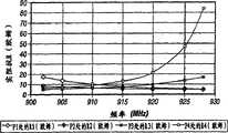
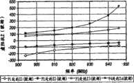
例如,图2A和2B示出了对于包括EAS元件1和RFID元件2的样品安全标签,相对于在915MHz ISM波段上的频率,RFID的天线阻抗的实分量和虚分量。For example, FIGS. 2A and 2B show the real and imaginary components of the antenna impedance of the RFID with respect to frequency in the 915 MHz ISM band for a sample security tag including
如在图2A中所示,在915MHz的中心频率处,实阻抗R当RFID标志2从位置P1移动到位置P4时,从R1=约6欧姆变化到R4=约13欧姆。实阻抗R的明显增加代表由于EAS标志材料而产生的有效损耗的增加。相应地,虚阻抗Z当RFID标志2从位置P1移动到位置P4时,从Z1=-125欧姆变化到Z4=+195欧姆。因此,虚阻抗Z从一定程度上的电容性特性变化到电感性特性。As shown in FIG. 2A, at a center frequency of 915 MHz, the real impedance R varies from R1 = about 6 ohms to R4 = about 13 ohms as the
RFID元件2可以被设计为使得天线阻抗接近ASIC设备的复共轭。这导致在目标频率、如915MHz的共振。对于由瑞士日内瓦的ST Microelectronics公司制造的芯片,在这个例子中使用了引线框,ASIC RFID设备的阻抗的典型测试结果为5-j140欧姆,对于由荷兰阿姆斯特丹的Koninklikje Philips Electronics N.V.公司制造的芯片,在这个例子中使用了引线框,典型测试结果为20-j270欧姆。对这两种RFID设备,需要RFID标志的天线虚阻抗Z在+j(140到270)欧姆的范围,以在目标频率实现谐振。The
因此,组合RFID/EAS安全标签可以使用EAS元件的阻抗为了匹配的目的被设计。在开放空间内,RFID元件天线可以被设计为具有负的虚阻抗,并且当被直接放置在EAS元件的下方、顶上或其附近时,得到正确的正虚阻抗。如通过本申请的公开内容可以认识到的,这种配置可以用于任何类型的EAS标签或标志,例如不同类型的粘性磁致伸缩标志和EAS硬标签,如由Sensormatic公司生产的
RFID元件例如可以包括半导体集成电路(IC)和可调谐天线。可调谐天线可以通过调节天线的长度被调谐到期望的工作频率。工作频率的范围可以改变,尽管所述实施例可能对超高频(UHF)频谱来说特别有用。根据应用和天线可用面积的尺寸,天线可以在几百兆赫(MHz)或更高范围内被调谐,如868-950MHz。在一个实施例中,例如,可调谐的天线可以被调谐,以在RFID操作频率内操作,如用于欧洲的868MHz波段,用于美国的915MHz工业、科学和医疗(ISM)波段,以及用于日本的950MHz波段。同样要注意的是,这些工作频率也只通过示例给出,所述实施例并不限于该上下文。RFID components may include, for example, semiconductor integrated circuits (ICs) and tunable antennas. A tunable antenna can be tuned to a desired operating frequency by adjusting the length of the antenna. The range of operating frequencies may vary, although the described embodiments may be particularly useful for the Ultra High Frequency (UHF) spectrum. Depending on the application and the size of the antenna's available area, the antenna can be tuned in the hundreds of megahertz (MHz) range or higher, such as 868-950MHz. In one embodiment, for example, the tunable antenna can be tuned to operate within RFID operating frequencies, such as the 868 MHz band for Europe, the 915 MHz Industrial, Scientific and Medical (ISM) band for the United States, and the Japan's 950MHz band. It is also to be noted that these operating frequencies are also given by way of example only and the described embodiments are not limited in this context.
在一个实施例中,例如,可调谐的天线可以具有内螺旋形式的独特的天线几何形状,这对于RFID应用或EAS应用都很有用。该内螺旋形式可以收拢天线轨迹,从而将这些天线轨迹带回到原点。这可以得到功能与传统的半波偶极子天线类似的天线,但整体尺寸更小。例如,在915MHz的传统半波偶极子天线的尺寸约为16.4厘米(cm)长。通过对比,一些实施例可以提供与在915MHz工作频率的传统半波偶极子天线相同的性能,而长度更短,约为3.81cm。此外,天线轨迹的末端可以被调整,以将该天线调谐到期望的工作频率。由于天线轨迹的末端是从天线周围向内的,该调谐不需要改变天线的几何形状就能实现。In one embodiment, for example, the tunable antenna may have a unique antenna geometry in the form of an internal helix, which is useful for either RFID applications or EAS applications. This inner helical form collapses the antenna traces, bringing them back to their origin. This results in an antenna that functions similarly to a conventional half-wave dipole antenna, but with a smaller overall size. For example, the size of a conventional half-wave dipole antenna at 915 MHz is about 16.4 centimeters (cm) long. By way of comparison, some embodiments can provide the same performance as a conventional half-wave dipole antenna operating at 915 MHz, but with a shorter length of approximately 3.81 cm. Additionally, the ends of the antenna trace can be adjusted to tune the antenna to a desired operating frequency. Since the ends of the antenna traces are inward from the perimeter of the antenna, this tuning can be achieved without changing the geometry of the antenna.
图3A示出了根据本发明的一个特别有用的实施例的第一系统。图3A示出了一个RFID系统100,它可以被配置为使用RFID元件2来工作,RFID元件2具有在高频(HF)波段中的工作频率,这个高频波段被认为是直到并包括30MHz的频率。在这个频率范围内,电磁场的主要成分是磁性的。然而,RFID系统100也可以被配置为使用其他部分的RF频谱来操作RFID元件2,如对于给定的实施方式所期望的那样。所述实施例并不限于该上下文。如通过示例所描述的,RFID元件2部分地叠盖EAS元件1。Figure 3A shows a first system according to a particularly useful embodiment of the present invention. FIG. 3A shows an
RFID系统100可以包括多个节点。在这里所使用的术语“节点”可以指系统、单元、模块、元件、电路板或设备,其可以处理表示信息的信号。该信号类型可以是,例如但不限于,属性上是电、光、声和/或化学的信号。尽管图3A示出了有限数目的节点,但可以认识到任何数目的节点都可以被用到RFID系统100中。所述实施例并不限于该上下文。
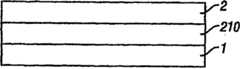
首先参考图4,图4示出了根据本发明的一个特别有用的实施例的安全标签200的侧视图。RFID元件2包括基底部分或底板202,它具有第一表面或表面区域202a以及第二表面或表面区域202b,它们通常位于基底部分或底板202的相对的两侧。天线204被放置在底板202上。天线204具有第一表面或表面区域204a以及第二表面或表面区域204b,它们通常位于天线204的相对的两侧。一个引线框206被放置在天线204上,一个专用集成电路(ASIC)208被放置在引线框206上。第一和第二表面或表面区域202a和202b、204a和204b被定义为RFID元件2的表面区域。Referring first to FIG. 4, a side view of a
安全标签200包括基本上为平面的覆盖材料或间隔物210,其被设置在RFID元件2上,而EAS元件1被放置在间隔物210上。间隔物210具有表面或表面区域202a和202b,位于其相对的两侧。The
EAS元件1具有第一表面或表面区域1a和第二表面或表面区域1b,它们通常位于EAS元件1的相对两侧。第一和第二表面或表面区域1a和1b被定义为EAS元件1的表面或表面区域。The
为了参照的目的,安全标签200被图示为被直接放置在EAS元件1的下面,即,在图1的位置P4。安全标签200仅通过示例在位置P4被示出,并且可以在相对于EAS标志1的任何位置放置,如先前针对图1所讨论的。安全标签200也可以完全独立于EAS标志1或者与其结合来使用。所述实施例并不限于该上下文。For reference purposes, the
更具体地说,安全标签200包括EAS元件1,它具有规定表面区域1a和1b之一,以及RFID元件2,它具有规定的表面或表面区域202a、202b、204a和204b之一。EAS元件1的规定表面或表面区域1a和1b中的至少一个被配置为至少部分地叠盖RFID元件2的规定表面或表面区域202a、202b、204a和204b中的至少一个。RFID元件2可以包括天线204,它至少部分地叠盖EAS元件1的规定表面或表面区域1a和1b中的至少一个。More specifically,
在一个实施例中,RFID元件2的规定表面或表面区域是表面或表面区域202a和202b中之一。In one embodiment, the defined surface or surface area of the
基本上为平面的间隔物210具有厚度“t”,并至少部分地放置在EAS元件1的规定表面或表面区域1a和1b中的至少一个、以及RFID元件2的规定表面或表面区域202a、202b、204a和204b中的至少一个之间。The substantially
虽然图4示出了有限数目的单元,但可以认识到,更大或更小数目的单元也可以被用于安全标签200。例如,粘性的和释放内衬(release liner)可以被加到安全标签200,以帮助将安全标签200贴到待监控的对象上。本领域技术人员将认识到,半导体IC 208可以直接被接合到天线204上,而不需要引线框206。While FIG. 4 shows a limited number of units, it will be appreciated that a greater or lesser number of units may also be used with
现在回到图3A,RFID系统100还可以包括RFID读取器102和安全标签200。安全标签200在物理上与RFID读取器102分开一段距离d1。如下参照图4所述,安全标签200是RFID安全标签、标签或标志,与现有技术的不同在于它包括一个EAS元件,即EAS标志或标签。RFID元件2包括谐振电路112。谐振电路112包括电感线圈L2,谐振电容C2跨接在ASIC 208的两端T1和T2。ASIC 208的电容与C2相比通常是可忽略的。如果需要对谐振电路112增加附加电容使得能够将所述天线,即电感线圈L2,调谐到合适的频率,一个电容C2与电感线圈L2并联连接,使得谐振电路112变成并联谐振电路,在其两端T1和T2可形成感生电压Vi。如下针对图4所述,终端T1和T2被耦合到RFID元件2的其它部分。另外,电感线圈或天线L2的电感值包括由EAS标志或标签所表现出的电感。Returning now to FIG. 3A ,
RFID读取器102可以包括调谐电路108,它具有电感L1,用作RFID读取器102的天线。当需要对调谐电路108增加附加电容,以使得能够适当地调谐电感线圈或天线L1时,一个电容C1与电感线圈或天线L1串联连接。RFID读取器102被配置为在调谐电路108两端产生脉冲的或连续波(CW)RF功率,通过交变电流动作被电磁耦合到RFID元件2的并联谐振电路天线112。来自RFID元件2的相互耦合的电磁功率通过磁场114被耦合到RFID读取器102。RFID reader 102 may include a
RFID元件2是一个功率转换电路,它将磁场114的一些耦合的CW RF电磁功率转换为直流信号功率,由半导体IC的逻辑电路用来实现对RFID元件2的RFID操作。The
RFID元件2也可以是RFID安全标签,它包括存储RFID信息的存储器,并且响应于一个询问信号104来传输所存储的信息。RFID信息可包括能够被存储在RFID元件2所使用的存储器中的任何类型的信息。例如,RFID信息包括唯一的标签标识符、唯一的系统标识符、被监控对象的标识符,等等。RFID信息的类型和数量并不限于该上下文。The
RFID元件2也可以是无源的RFID安金标签。无源的RFID安全标签不使用外部电源,而是使用询问信号104作为电源。检测区Z1被定义为由通常为球状的表面所限定的空间的假想区域,该空间的半径R1通常源自电感线圈L1。半径R1定义了检测距离或读取范围R1,使得当距离d1小于或等于读取范围R1时,RFID读取器102在两端T1和T2会感应出一个所需要的门限电压VT,以激活RFID元件2。在各种因素中,读取范围R1取决于来自调谐电路208的EM场辐射和磁场114的强度。因此,EM场辐射114的强度决定了读取范围R1。The
RFID元件2可以通过对包含询问信号104的输入RF载波信号进行整流而产生的直流电压被激活。一RFID元件2被激活,它可以经由响应信号110传输存储在其存储寄存器中的信息。The
在一般的高频(HF)操作中,当RFID系统100的谐振电路112接近RFID读取器102的调谐电路108时,在RFID元件2的并联谐振电路112的两端T1和T2产生交流(AC)电压Vi。谐振电路112两端的AC电压Vi被整流器整流为直流(DC)电压,并且当经过整流的电压幅度达到门限值VT时,RFID元件2被激活。整流器是上述的专用集成电路(ASIC)208。一旦被激活,RFID元件2通过调制RFID读取器102的询问信号104以形成响应信号110,来发送存储在其存储寄存器中的数据。然后RFID设备106将响应信号110发送到RFID读取器102。RFID读取器102接收响应信号110并将其转换为被检测的串行数据字比特流数据,代表来自RFID元件2的信息。In general high frequency (HF) operation, when the
如图3A中所示出的RFID系统100可以被认为是高频(HF)RFID系统,因为RFID读取器102经由磁场114电感耦合到RFID元件2。在HF应用中,天线204典型地是电感线圈型天线,如电感线圈L2所提供的。
图3B示出了超高频(UHF)RFID系统150,其中RFID读取器152经由磁场E耦合到有一定距离d2处的RFID设备、标签或标志156。在这里UHF的频段被认为是从约300MHz到约3GHz的范围内。该UHF的范围具体包括在868MHz波段、915MHz波段和950MHz波段中的频率。Figure 3B shows an ultra high frequency (UHF)
对于UHF应用,RFID元件2的天线204典型地包括一个UHF终端开路(open-ended)偶极子天线,而RFID读取器152典型地包括一个补片天线。从读取器152引出的同轴馈电线被连接至补片天线。UHF天线可以是简单的半波偶极子天线或补片天线。很多流行的设计使用填充有空气的腔体支持的补片天线,其可以是线性极化的也可以是圆极化的。对于圆极化的情形,电场矢量E1和E2以相等的幅度旋转。被线性极化的天线在特定的正交方向上具有更高的E场幅度,可以适合某些特定RFID标志定向。For UHF applications, the
因此,在UHF应用中,RFID元件2的天线204包括UHF终端开路偶极子天线,而在HF应用中,典型地是电感L2。Thus, in UHF applications, the
总之,当在UHF范围内工作时,RFID元件2不必包括诸如与终端开路偶极子天线204并联的电容C2,使得能够调谐到由RFID读取器152的补片天线所发送的频率。In conclusion, when operating in the UHF range, the
回到图4,如先前所提到的,RFID元件2可以包括基底部分或底板202,它包括任何类型的适合于装配天线204、引线框206和IC 208的材料。例如,底板202的材料可以包括原纸、聚乙烯、聚酯、聚对苯二甲酸乙二醇酯(PET)、聚醚酰亚胺(PEI)(例如,康涅狄格州Fairfield的通用电气公司销售的
总之,当与不存在底板的开放空间相比时,更高的介电常数可能会导致天线的更大的频移。虽然可能能够通过以物理方式改变天线方向图将天线重调谐到最初的中心频率,可能希望有一种具有高介电常数和低介电损耗的材料,因为使用这种材料会得到更小的标签或标志尺寸。术语“读取范围”可以指RFID读取器102和安全标签200之间的通信工作距离。安全标签200的读取范围例如可以是1-3米,虽然所述实施例并不限于该上下文。损耗因数可以表示电介质对RF能量的吸收特性。被吸收的能量可能作为热量被损失掉,并且可能不能由ASIC 208使用。损失掉的能量可能导致与降低所传输的功率相同的影响,并可能相应地降低读取范围。因此,可能希望在底板202中具有尽可能低的损耗因数,因为不能通过调节天线204“失调”。总的频移和RF损耗也可能取决于底板202的厚度。随着厚度的增加,频移和损耗也可能增加。In conclusion, a higher dielectric constant may lead to a larger frequency shift of the antenna when compared to an open space without a backplane. While it may be possible to retune the antenna to its original center frequency by physically changing the antenna pattern, it may be desirable to have a material with a high dielectric constant and low dielectric loss, since using this material would result in a smaller tag or Logo size. The term “read range” may refer to the communication working distance between the RFID reader 102 and the
例如在一个实施例中,底板202也可以用原纸来配置,它具有约3.3的介电常数,以及约0.135的损耗因数。原纸可能在900MHz相对致损。致损材料具有大于约0.01的介电损耗因数。在一个实施例中,底板202也可以用塑料来配置,它具有约3.3的介电常数,以及小于约0.01的损耗因数。所述实施例并不限于该上下文。For example, in one embodiment,
在一个实施例中,安全标签200可以包括IC 208,它具有半导体IC,诸如RFID芯片或专用集成电路(ASIC)(“RFID芯片”)。RFID芯片208例如可包括将RF或AC电压转换为DC电压的RF或交流(AC)整流器,用来将所存储的数据传输到RFID读取器的调制电路,存储信息的存储器电路,以及控制设备的整体功能的逻辑电路。在一个实施例中,RFID芯片208可以被配置为使用I-CODE高频智能标志(HSL)RFID ASIC或U-CODE超高频智能标志(USL)RFID ASIC,两者都由荷兰阿姆斯特丹的飞利浦半导体公司制造,或者是瑞士日内瓦的ST Microelectronics公司制造的XRA00 RFID芯片。然而所述实施例并不限于该上下文。In one embodiment,
引线框为小的连接,其允许将诸如RFID芯片208的RFID芯片附加到诸如天线204的天线上。在一个实施例中,RFID芯片208可以被直接接合到天线204上,而不需要包括引线框206。引线框206也可以包括模座叶片(die mounting paddle)或板层(flag),以及多个引脚(lead finger)。模座叶片主要用来在制造包装期间机械地支撑模座。所述引脚将模座连接到包装外部的线路。每个引脚的一端典型地通过线接合或带状自动接合连接到底座上的接合垫。各引脚的另一端是引线,其通过机械方式和电气方式连接到底板或电路板上。引线框206可以通过冲压或蚀刻由金属片制成,通常接着进行诸如电镀、座陷成型(downset1)、卷带等最终处理。在一个实施例中,例如,引线框206可以使用佛罗里达州Boca Raton的Tyco Fire and Security有限公司的分公司,Sensormatic公司生产的Sensormatic EASMicrolabelTM引线框来实现。然而,所述实施例并不限于该上下文。A lead frame is a small connection that allows an RFID chip such as
在一个实施例中,天线204包括电感线圈L2,以及当需要时,还包括RFID元件2的谐振电路112的电容C2。终端T1和T2也被包括在天线204中,以耦合到RFID芯片208,使得一旦达到门限电压VT,感生出的电压Vi能够激活RFID元件2。In one embodiment, the
在一个实施例中,天线204典型地包括用于UHF应用的RFID元件2的终端开路偶极子天线。终端T1和T2也可以被包括在天线204中,以耦合到RFID芯片208,使得电场E激励读取器152的天线。In one embodiment,
在一个实施例中,安全标签200也可以包括覆盖或间隔材料210,其被敷设到加工后的安全标签的顶部。如同底板202一样,覆盖或间隔材料210也可能影响RFID元件2的RF性能。例如,覆盖材料210可以使用表面材质(cover stock material)来实现,它具有约3.8的介电常数和约0.115的损耗因数。所述实施例并不限于该上下文。In one embodiment, the
更特别地,如前所述,基本上为平面的间隔物210具有厚度“t”。当安全标签200为硬组合标签时,厚度“t”通常为约1mm到2mm,当安全标签200为组合标志时,其厚度大大小于1mm。如先前所述,间隔物210具有位于其相对的两侧的表面或表面区域210a和210b。在一个实施例中,间隔物表面或表面区域210a和210b相互平行。EAS元件1至少部分地叠盖间隔物表面或表面区域210a和210b中的至少一个。More particularly, the substantially
RFID插件是本技术领域中的常用术语,在这里被定义为RFID元件2,其包括底板202、天线204、引线框206(如果有的话)和RFID芯片208的组合。RFID元件2至少部分地叠盖了间隔物表面中的另一个表面210b。安全标签200包括RFID插件或元件2和间隔物210。An RFID interposer is a commonly used term in this technical field, and is defined here as an
安全标签200也可以包括天线204。天线204例如可以代表RFID设备106的天线112,或者天线204可以由并联谐振LC电路形成,这里L是电感,C是电容。作为替代,天线204也可以是可调谐天线,其被调谐至载波信号,使得天线电路两端的电压最大。如可以理解的,这将增加天线204的读取范围。已知调谐电路的精确程度与由发送器102发送的载波信号的频谱宽度有关。例如在美国,联邦通信委员会(FCC)目前将RFID安全标签频谱的一个波段调节到915MHz。因此,发送器102应该在大约915MHz发送询问信号104。为了接收询问信号104,天线204应该被很窄地调谐到915MHz的信号。对于915MHz的应用,RFID标签天线204可以被印刷、蚀刻或电镀。
EAS标志1对RFID元件2产生或表现出恒定的负载阻抗。结果,RFID标志200的天线204使用该EAS标志1的恒定负载用于阻抗匹配。更特别地,天线204具有复阻抗,并且EAS元件1形成了天线的一部分阻抗匹配网络。因此,天线204的阻抗包括EAS元件1的加载效应。即,EAS元件1的加载效应为EAS元件1的恒定负载阻抗。可以通过用一种被包含在EAS元件1中的具有一定介电常数和损耗因数的材料来代替或替换具有其他介电常数和损耗因数的另一种材料来改变EAS元件1的加载效应。The
RFID元件芯片208可以被表示为等效串联RC电路,其中R表示电阻,C表示电容。该电路由复阻抗Zchip表示为:The
Zchip=Z1-jZ2,Zchip = Z1 −j Z2 ,
其中Z1和Z2为芯片208的阻抗的实部和虚部。RFID设备标签或标志天线204可以用复阻抗Zantenna被表示为:where Z1 and Z2 are the real and imaginary parts of the impedance of
Zantenna=Z3+jZ4 (1)Zantenna =Z3 +jZ4 (1)
其中Z3和Z4为天线204的阻抗的实部和虚部。当芯片208被装配在天线204上时,芯片208的复阻抗与RFID天线204的耦合共轭阻抗相匹配,包括EAS元件或标志1的阻抗匹配效应或加载效应。这允许耦合到RFID芯片208的最大功率,它得到了最大的读取范围R1。Where Z3 and Z4 are the real and imaginary parts of the impedance of the
在一个实施例中,间隔物210的厚度“t”可以相对于RFID读取器设备102或者相对于RFID读取器设备152而改变,以分别改变读取范围R1。更特别地,厚度“t”确定了读取范围,即安全标签200和EAS/RFID读取器102或EAS/RFID读取器152之间的最大距离R1,读取器102或152能够以该距离询问安全标签200。读取范围R1随着厚度“t”的减小反过来受到影响。相反地,读取范围R1随着厚度“t”的增加而增加。In one embodiment, the thickness "t" of the
参照图4和4A,图4A分别示出了实际数据41和曲线拟合数据和42,其对应于安全标签,如在硬标签外壳(如图8D中的外壳812或图8F中的外壳818,如下所述)内的由诸如EAS元件1的EAS单元和诸如RFID元件2的RFID单元构成的安全标签200。间隔物210被放置在EAS元件1和RFID元件2之间,可由低损耗、低介电材料或空气间隙形成。在图4A中所示数据的特定情形下,间隔物210为空气间隙。y轴显示了以米(m)为单位的读取范围R1,而x轴显示了以毫米(mm)为单位的诸如间隔物210的间隔物的厚度“t”。实际数据41和曲线拟合数据42示出了当间隔物的厚度“t”增加到20mm或更大时,读取范围R1基本上为恒定,约1.8米。随着间隔物的厚度“t”被减小到约3mm的数值时,读取范围R1减少到约1米。读取范围R1随着间隔物厚度“t”的减小而继续减少,因为EAS元件1中的损耗随着减少的间隔物厚度“t”变得更大。Referring to Figures 4 and 4A, Figure 4A shows actual data 41 and curve fitting data and 42, respectively, corresponding to a security tag, such as a hard tag housing such as housing 812 in Figure 8D or
如先前针对图4所述,在组合EAS和RFID标签或标志200中,EAS元件1和RFID元件2至少部分重叠,并且EAS元件1是RFID天线204的一部分阻抗。另外,参照图3A、3B和4,位于RFID元件2和EAS元件1之间的对应于厚度“t”的间隔物210可以被用来从RFID读取器102确定RFID元件2的读取范围R1。此外,厚度“t”可以被改变,以根据特定应用在各种优选的水平建立读取范围R1。因此,间隔物210和相应的厚度“t”确定了读取范围R1,并且作为组合EAS和RFID标签或标志200的控制单元起作用,或者换句话说,间隔物210的厚度“t”是可配置的,以调节RFID读取器102和RFID元件2之间的读取范围R1。As previously described with respect to FIG. 4 , in combination EAS and RFID tag or
由于图4A中出现的数据是特别针对间隔物210是空气间隙的情形,可以认识到,读取范围R1和间隔物210厚度“t”之间的关系对于为间隔物210所选择的其它低损耗、低介电材料的情形会不同。Since the data presented in FIG. 4A is specifically for the case where
需要注意到的是,用于HF应用的读取器102和用于UHF的读取器152只读取EAS元件1或者只读取RFID元件2,使得EAS元件1被专用的EAS读取器读取,而RFID元件2被专用的RFID读取器读取。作为替代,读取器102和读取器152可以被组合到同一个外壳中,或者它们的功能被整合以被同一个硬件执行。由于EAS元件所共有的读取频率范围相对于RFID元件所共有的读取频率范围之间有较大的差异,EAS元件1的读取和RFID元件2的读取之间不希望的干扰被避免或被最小化,EAS元件典型地在小于或等于8.2KHz的频率范围内被读取,而RFID元件典型地在13KHz或更大的频率范围内的被读取。It should be noted that the reader 102 for HF applications and the
然而,可以看出,由于安全标签200和400为独立的设备,安全标签200和400提供了EAS功能和RFID功能,而与读取器的类型、或者安全标签200或400所处的读取器或特定频率无关。However, it can be seen that since the security tags 200 and 400 are stand-alone devices, the security tags 200 and 400 provide the EAS function and the RFID function, regardless of the type of reader, or the reader in which the
间隔物210使用诸如由马萨诸塞州Randolph的EmersonCuming Microwave Products公司制造的
在一个实施例中,间隔物210可以是厚度“t”约为0.05mm的薄膜,其中EAS元件1直接叠盖RFID元件2。In one embodiment, the
在一个实施例中,间隔物可以是空气,其中EAS标志1被以机械方式支持、与RFID元件2隔开。In one embodiment, the spacer may be air, wherein the
结果,安全标签200通过提供具有明显更低的空间或体积和更低成本的组合EAS/RFID设备,相对于现有技术提供了显著的优势。As a result,
在一个实施例中,安全标签200可以使用来自线圈天线的感生电压来工作。这个感生出的AC电压可以被整流为DC电压。当DC电压达到一个特定水平时,RFID元件2开始工作。通过经由发送器102提供激励RF信号,RFID读取器102可以与位于远端的、没有诸如电源的外部电源的安全标签200通信。In one embodiment,
由于RFID读取器和RFID元件2之间的激励和通信是通过天线204来完成的,天线204可以为改善RFID应用而被调谐。如果天线的线尺寸与工作频率的波长可比,RF信号可以被有效地发射或接收。然而,线尺寸可能会大于天线204可用的表面区域。因此,可能会很难在有限的空间内使用真正完全尺寸的天线,对大多数HF应用中的RFID系统都是这样。因此,可以预期RFID元件2可以使用更小的LC环形天线电路,被配置为在给定的工作频率谐振。LC环路天线例如可以包括螺旋线圈和电容。螺旋线圈典型地由n匝线或者介电底板上的n匝印刷或蚀刻的电感线圈的形成。Since the excitation and communication between the RFID reader and the
对于HF应用,为了实现良好的RFID耦合,环路区域匝产品和谐振频率需要被优化。在图3A中所示的本发明的一个实施例中,谐振频率可以通过调谐谐振电路112的并联电容C2受到影响,包括对EAS标志1和RFID芯片208的阻抗的影响。For HF applications, the loop area turn product and resonant frequency need to be optimized for good RFID coupling. In one embodiment of the invention shown in FIG. 3A , the resonant frequency can be influenced by tuning the parallel capacitance C2 of the
在HF或UHF应用中,对于感兴趣的特定频率,RFID芯片复阻抗必须与天线的复共轭阻抗相匹配,包括对EAS标志的阻抗的加载效应。在HF的情形中,谐振电容通常被用来调谐频率。该电容通常大于RFID芯片的电容,并且会支配该响应。在UHF的情形中,RFID芯片的复阻抗只包含用于调谐的芯片电容。In HF or UHF applications, for the specific frequency of interest, the complex impedance of the RFID chip must match the complex conjugate impedance of the antenna, including the loading effect on the impedance of the EAS marker. In the case of HF, a resonant capacitor is usually used to tune the frequency. This capacitance is usually larger than that of the RFID chip and will dominate the response. In the case of UHF, the complex impedance of the RFID chip contains only the chip capacitance for tuning.
在根据本发明的另一个实施例中,天线204可以被设计为在期望的工作频率、例如915MHz的频率下使得整个天线的复共轭阻抗匹配于引线框206和IC 208的复阻抗。然而,当RFID安全标签200被放置在被监控的对象上时,已经发现所得到的工作频率可能会改变,即每个目标的底板材料的介电特性可能会影响天线204的RF性能。换句话说,和底板202一样,目标底板可能会引起由介电常数、损耗因数和材料厚度所决定的频移和RF损耗。不同的目标底板例如可包括被称为“粗纸板(chip board)”(即用于产品级(item-level)纸板箱的材料,作为用于瓦楞纸板箱的材料的瓦楞纸板),录像带和数字化视频光盘(DVD)盒、玻璃、金属等。预期每个目标底板对安全标签200的读取范围R1可能有显著的影响。In another embodiment according to the present invention, the
天线204可以是可调谐的,以补偿这种变化。换句话说,既然很多材料的介电常数大于1,当工作标签200被贴到目标底板上时,工作频率往往会降低。为了建立原始频率,天线204典型地以某种方式被改变,否则检测性能和读取范围可能会降低。同样,可以通过修整天线204的末端、切断天线导线、并将得到的修整过的天线段从被切除的末端脱离开来改变天线204。被修整过的末端不必被移除以允许调谐操作。因此,将天线204连续地调谐到期望的工作频率是可能的,当安全标签200被附加到不同的目标时,允许安全标签200工作。以下将参照图5-7更详细地对安全标签200在整体上、以及针对天线204具体地进行说明。
图5示出了根据本发明的一个实施例的带有天线的部分安全标签200的顶视图,它尤其适合于UHF应用。安全标签200包括被设置在基本上为矩形的底板202上的天线204。在一个预想的实施例中,天线204通过冲切标志天线方向图到底板202上而被设置在底板202上。Figure 5 shows a top view of a portion of a
RFID芯片208可以通过将引线框206超声接合到RFID芯片208上的传导垫来连接到引线框206。在图5的特定实施例中,RFID芯片208和引线框206被放置在底板202的介电底板材料的几何中心。引线框206的末端以机械方式和电气方式接合到天线204的薄膜天线方向图。一种覆盖材料(未示出)可以被敷设到安全标签200的整个顶部表面,以保护组件并提供表面以在需要的时候印刷标志。在本技术领域中已知使用各向异性电传导热安装粘合剂来将RFID芯片208粘合到天线204上。这种粘合剂的一个例子是由康涅狄格州Rocky Hill的Henkel Loctite公司制造的Loctite
第一天线部分306可以具有第一天线末端306A和第二天线末端306B。类似地,第二天线部分308可以具有第一天线末端308A和第二天线末端308B。在一个实施例中,如图5中所示,第一天线部分306的第一天线末端306A被连接到引线框206A。第一天线部分306被设置在底板202上,以形成从RFID芯片208在第一方向上的内螺旋图样,第二天线末端306B被放置以在所述内螺旋图样的内环上终止。类似地,第二天线部分308的第一天线末端308A可以被连接到引线框206B。第二天线部分308也被放置在底板202上,以形成从RFID芯片208在第二方向上的内螺旋图样,第二天线末端306B被放置以在内螺旋图样的内环上终止。The
在一个实施例中,天线204的天线几何形状被配置为横过底板202的周边,并向内螺旋。可以看出,向内螺旋的天线方向图可以提供几个优点:In one embodiment, the antenna geometry of the
(1)天线204的末端可以被很好地放置在底板202的周边内。将天线204的末端放置在底板202的周边内可以允许末端被修整,而不需要改变天线204所占用的面积;(1) The end of the
(2)天线204的Q因子可以被优化,使得安全标签200的响应,包括间隔物210和EAS标志1的影响,只在ISM波段限制处改变大约-3dB。使用Chu-Harrington限制,Q=1/(ka)3+1/(ka),其中k=2π/λ,“a”是天线204的特征尺寸,可以看到,半径为“a”的球能够刚好围绕安全标签200。对于高的Q因子,“ka”应该<<1。因此,通过最大化Q,“a”被最小化,以落入工作频率波段限制之内。对于UHF应用,天线204的调谐在由R.Copeland和G.M.Shafer在2004年8月13日提交的,名为“TUNABLE ANTENNA”的共同待审的、共有美国专利申请序列号10/917752中被更详细地公开,其整个内容在这里并入以作参考。(2) The Q factor of the
特别是对于UHF应用,也可以通过改变第一天线部分306的第一长度以及第二天线部分308的第二长度,当这些天线部分被设置在底板202上之后,将天线204调谐到期望的工作频率。例如,每个天线部分可以在多个分段点被划分为多个天线段。第一和第二天线长度可以通过将至少第一天线段从第二天线段电脱离开而被改变。天线长度可以通过在多个分段点之一处切割出各个天线部分而被修改,各个分段点对应天线204的工作频率。将第一天线部分306和第二天线部分308划分为多个天线段会导致各个天线部分的长度的缩短,从而有效地改变天线204的总电感。天线段和分段点将参照图6更详细地说明。Especially for UHF application, also can be by changing the first length of
图6示出了根据一个实施例的安全标签400的视图,它带有具有分段点的天线。特别地,图6示出了带有多个分段点SP1、SP2、SP3和SP4的安全标签400的各部分的顶视图。以和图4中关于安全标签200类似的方式,安全标签400可以包括EAS元件1、间隔物210和RFID元件2。也可以通过改变第一天线部分306的第一长度以及第二天线部分308的第二长度,当这些天线部分被设置在底板202上之后,将天线204调谐到期望的工作频率。例如,预期每个天线部分可以在多个分段点SP1-SP4处被划分为多个天线段。多个分段点SP1至SP4代表末端调谐位置,在这里天线204可以被切割或剪切,以对各种目标进行调谐。SP1是原始开放空间天线204的长度被调谐到868MHz的开放空间位置。SP2是天线部分306和308的长度被调谐到915MHz的开放空间位置。SP3和SP4是天线部分306和308的长度对各种目标进行调谐的开放空间位置。所述各种目标包括,例如但不限于,零售和/或批发商品。Figure 6 shows a view of a
第一和第二天线的长度可以通过将至少第一天线段从第二天线段电脱离开而被改变。天线长度可以通过在多个分段点之一处切割出各个天线部分而被修改,各个分段对应天线204的工作频率。所述切断可以通过若干不同的方式来实现,诸如在给定分段点SP1-SP4处切割或冲出天线轨迹。所述切割可能在分段点产生槽,诸如槽402、404、406、408、410和412。The lengths of the first and second antennas may be varied by electrically decoupling at least the first antenna segment from the second antenna segment. The antenna length may be modified by cutting individual antenna sections at one of a plurality of segment points, each segment corresponding to the operating frequency of the
需要注意的是,对于HF应用,天线204可以通过改变电感或电容参数、而不是各分段的长度而被调谐。It should be noted that for HF applications, the
在一个实施例中,如图6中所示,每个分段点SP1-SP4对应于天线204的一个工作频率。在一个示例中,当安全标签400位于开放空间中并且未附加到目标上时,SP1可以对约868MHz的工作频率调谐天线204。当安全标签400位于开放空间中并且未附加到目标上时,SP2可以对约915MHz的工作频率调谐天线204。当安全标签400被附加到VHS盒带外壳上时,SP3可以对约915MHz的工作频率调谐天线204。当安全标签400被附加到粗纸板上时,SP4可以对约915MHz的工作频率调谐天线204。可以理解,分段点的数目和天线204的相应工作频率可以根据给定的实施方式改变。所述实施例并不限于该上下文。In one embodiment, as shown in FIG. 6 , each segment point SP1 - SP4 corresponds to an operating frequency of the
图7示出了根据本发明的另一个实施例的方框流程图500。如先前所述,安全标签200可以用若干方式被配置。例如:1)在方框502集成电路可以被连接到引线框;2)在方框504天线可以被放置在底板上;3)在方框506引线框可以被连接到天线。FIG. 7 shows a block flow diagram 500 according to another embodiment of the present invention. As previously mentioned,
在一个特定的实施例中,天线在方框508被调谐,从而以工作频率被使用。该调谐可以通过将天线在对应工作频率的分段点处切割成多个天线段从而改变天线的长度来实现。所述切割可以将第一天线段从第二天线段电气分离,从而有效地缩短天线长度。In a particular embodiment, the antenna is tuned at block 508 to be used at the operating frequency. The tuning can be realized by cutting the antenna into multiple antenna segments at a segment point corresponding to the working frequency so as to change the length of the antenna. The cut can electrically separate the first antenna segment from the second antenna segment, effectively shortening the antenna length.
如上所述,当被连接到RFID芯片时,内螺旋图样的独特的天线几何形状对于RFID应用可能是有用的。然而如先前所述,图5和6中所示出的独特的天线几何形状也可能对EAS系统有用,在这里安全标签200和安全标签400分别包括EAS元件1和间隔物210。在一个实施例中,RFID芯片208可以用二极管或其它非线性无源设备来代替,其电压和电流特性是非线性的。用于二极管或其它无源非线性EAS设备的天线可具有与图5和6中所示相同的几何形状,并且可以被修整以将天线调谐到发送器的工作频率,用来为EAS系统发送询问信号。与RFID系统100类似,工作频率的范围可以改变,虽然所述实施例可能对UHF频谱、如868-950MHz尤其有用。所述实施例并不限于该上下文。As mentioned above, the unique antenna geometry of the inner helical pattern may be useful for RFID applications when connected to an RFID chip. However, as previously stated, the unique antenna geometry shown in Figures 5 and 6 may also be useful for EAS systems, where
如先前针对图3A、3B、4和4A所述,组合EAS和RFID标签或标志200的读取范围R1可以通过改变间隔物210的厚度“t”被测量、控制和改变。以类似的方式,安全标签400的读取范围R1也可以通过改变间隔物210的厚度“t”被测量、控制和改变。As previously described with respect to FIGS. 3A , 3B, 4 and 4A, the read range R1 of the combination EAS and RFID tag or tag 200 can be measured, controlled and varied by varying the thickness “t” of the
也可以预期,本发明的一些实施例可以使用根据任意数目的因素而不同的架构被配置,这些因素诸如:1)期望的计算速率;2)功率水平;3)耐热性;4)处理周期预算;5)数据输入率;6)数据输出率;7)存储资源;8)数据总线速度和其它性能约束。例如,实施例可以使用由通用或专用处理器所执行的软件来配置。在另一个例子中,实施例可以被配置为专用硬件,如电路、ASIC、可编程逻辑设备(PLD)或数字信号处理器(DSP)。在另外一个例子中,实施例可以通过编程的通用计算机元件和定制的硬件元件的任意组合来配置。所述实施例并不限于该上下文。It is also contemplated that some embodiments of the invention may be configured using architectures that vary according to any number of factors, such as: 1) desired computing rate; 2) power level; 3) thermal tolerance; 4) processing cycle time 5) data input rate; 6) data output rate; 7) storage resources; 8) data bus speed and other performance constraints. For example, an embodiment may be configured using software executed by a general-purpose or special-purpose processor. In another example, an embodiment may be configured as dedicated hardware, such as a circuit, ASIC, programmable logic device (PLD), or digital signal processor (DSP). In another example, an embodiment may be configured by any combination of programmed general-purpose computer components and custom hardware components. The embodiments are not limited in this context.
安全标签200和400的例子,即组合EAS和RFID标志/标签,在图8A到8D中示出,它们示出了各种类型的粘性的磁致伸缩标志和EAS硬标签,如由Sensormatic公司生产的
在图8A和8B的配置中,EAS标志804和RFID标志806在阻抗值匹配方面相互独立地工作。随着“g”增加,读取范围增加。结果,间隙“g”的尺寸控制了阻抗负载。然而,这并不是期望的效果,因为虽然读取范围增加了,EAS标志804和RFID标志806所占据的总面积也增加,需要在待识别的对象上占据更多的空间或面积。In the configuration of Figures 8A and 8B, the
图8C示出了本发明所述的安全标签200或400的一个实施例,示出了EAS元件或标志1。一个RFID元件或插件2被直接装配在EAS元件或标志1之下。虚拟(dummy)条形码802被印刷在EAS元件或标志1上,并且仅用于可视的目的。虚拟条形码802不具有EAS或RFID功能。与现有技术相比,安全标签200或400的配置作为EAS元件或标志或标签1与RFID元件或插件2的组合,被直接装配在EAS元件或标志1之下(如图4所示),提供了RFID元件或插件2与EAS标志1之间的最小隔离。FIG. 8C shows an embodiment of a
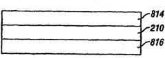
图8D示出了本发明的一个实施例,即EAS元件或标志1与RFID元件或插件2的组合的外壳的一部分812。RFID元件或插件2被定义为包括安装在天线204上的RFID芯片208。然而,间隔物210或粘性层并不可见(见图4)。FIG. 8D shows an embodiment of the present invention, a part 812 of a housing of a combination of an EAS element or
图8E是图8D中所公开的EAS元件或标志1与RFID元件或插件2的组合的正视图,但示出了被放置在EAS元件或标志1与RFID元件或插件2之间的间隔物210。Figure 8E is a front view of the combination of the EAS element or
图8E示出了本发明的一个实施例,即和EAS元件或标志1类似的EAS标志816与和RFID元件或插件2类似的RFID插件814的组合的外壳的一部分818。RFID插件814被定义为安装在天线204上的另一个RFID芯片820。同样,间隔物210或粘性层并不可见(见图4)。FIG. 8E shows a
图8G是在图8F中所公开的EAS标志816与RFID插件814的组合的正视图,但示出了被放置在EAS标志816和RFID插件814之间的间隔物210。8G is a front view of the combination of
EAS设备和RFID组合的类型并不限于在这里所述的EAS和RFID设备。The type of EAS device and RFID combination is not limited to the EAS and RFID devices described herein.
也可以预见,不仅间隔物的厚度是可配置的,用于改变组合EAS/RFID标签的RFID元件的有效读取范围,而且也可以预见,改变间隔物的厚度或形状可以影响RFID元件的读取范围。此外,也可以预见,被放置在EAS和RFID元件之间的间隔物可能由多种不同的低损耗、低介电材料制成,它可以排列在表面上,以影响EAS和RFID元件中的一个或两者的读取范围。也可以预见,间隔物的材料类型可以改变EAS元件和RFID元件的读取范围。更进一步,可以预见,间隔物(或多个间隔物)可以被配置为不同的几何形状配置或图样,带有不同的或变化的维度(即长度、宽度、厚度等等),以根据特定目来影响读取范围,或者进一步调节EAS和RFID元件中的一个或两者的读取范围。It is also foreseeable that not only the thickness of the spacer is configurable for changing the effective read range of the RFID element of the combination EAS/RFID tag, but it is also foreseeable that changing the thickness or shape of the spacer can affect the reading of the RFID element scope. In addition, it is also envisioned that spacers placed between the EAS and RFID components may be made of a variety of different low-loss, low-dielectric materials, which may be arranged on the surface to affect one of the EAS and RFID components. or the read range of both. It is also contemplated that the type of material of the spacer can alter the read range of the EAS element and the RFID element. Still further, it is envisioned that the spacer (or spacers) may be configured in different geometric configurations or patterns, with different or varying dimensions (i.e., length, width, thickness, etc.) to affect the read range, or to further adjust the read range of one or both of the EAS and RFID components.
虽然所述实施例的某些特征如这里所说明的那样进行了阐述,但很多修改、替换、变动和等价物将被本领域技术人员想到。因此可以理解,附加的权利要求将要覆盖所有这些在所述实施例的真正主旨范围内的修改和变动。While certain features of the described embodiments have been set forth as described herein, many modifications, substitutions, changes and equivalents will occur to those skilled in the art. It is therefore to be understood that the appended claims are to cover all such modifications and changes as fall within the true spirit of the described embodiments.
Claims (8)
Applications Claiming Priority (3)
| Application Number | Priority Date | Filing Date | Title |
|---|---|---|---|
| US62830304P | 2004-11-15 | 2004-11-15 | |
| US60/628,303 | 2004-11-15 | ||
| PCT/US2005/041575WO2006055655A1 (en) | 2004-11-15 | 2005-11-15 | Combination eas and rfid label or tag with controllable read range |
Publications (2)
| Publication Number | Publication Date |
|---|---|
| CN101088109A CN101088109A (en) | 2007-12-12 |
| CN101088109Btrue CN101088109B (en) | 2010-06-16 |
Family
ID=35994664
Family Applications (2)
| Application Number | Title | Priority Date | Filing Date |
|---|---|---|---|
| CN2005800447245AActiveCN101088109B (en) | 2004-11-15 | 2005-11-15 | Combined EAS and RFID tag or label with controllable read range |
| CNB2005800453246AActiveCN100552736C (en) | 2004-11-15 | 2005-11-15 | Combination eas and RFID tag or label |
Family Applications After (1)
| Application Number | Title | Priority Date | Filing Date |
|---|---|---|---|
| CNB2005800453246AActiveCN100552736C (en) | 2004-11-15 | 2005-11-15 | Combination eas and RFID tag or label |
Country Status (10)
| Country | Link |
|---|---|
| US (2) | US7804407B2 (en) |
| EP (2) | EP1817757A1 (en) |
| JP (2) | JP2008521098A (en) |
| KR (1) | KR101166598B1 (en) |
| CN (2) | CN101088109B (en) |
| AU (2) | AU2005307753B2 (en) |
| BR (1) | BRPI0518913B1 (en) |
| CA (2) | CA2587502C (en) |
| ES (1) | ES2564168T3 (en) |
| WO (2) | WO2006055653A1 (en) |
Families Citing this family (70)
| Publication number | Priority date | Publication date | Assignee | Title |
|---|---|---|---|---|
| US7557433B2 (en) | 2004-10-25 | 2009-07-07 | Mccain Joseph H | Microelectronic device with integrated energy source |
| US7812729B2 (en)* | 2004-11-15 | 2010-10-12 | Sensormatic Electronics, LLC | Combination EAS and RFID label or tag with controllable read range using a hybrid RFID antenna |
| US7804411B2 (en)* | 2004-11-15 | 2010-09-28 | Sensormatic Electronics, LLC | Combination EAS and RFID label or tag using a hybrid RFID antenna |
| JP4873868B2 (en)* | 2005-02-09 | 2012-02-08 | ルネサスエレクトロニクス株式会社 | Passive RFID semiconductor device, IC tag, IC tag control method, and communication method |
| DE102005054496B3 (en)* | 2005-11-16 | 2007-05-03 | Koenig & Bauer Ag | Electronic dataset generating method, for use in handling chain of printing machine, involves evaluating dataset from printing press or based on return of tag to manufacturer of substrate for objection or return delivery process |
| US8461992B2 (en)* | 2006-05-12 | 2013-06-11 | Solstice Medical, Llc | RFID coupler for metallic implements |
| WO2008076464A2 (en)* | 2006-06-21 | 2008-06-26 | Surgisense Corporation | Wireless medical telemetry system and methods using radio-frequency energized biosensors |
| US8674888B2 (en)* | 2006-06-21 | 2014-03-18 | Broadcom Corporation | Integrated circuit with power supply line antenna structure and methods for use therewith |
| WO2008013245A1 (en)* | 2006-07-26 | 2008-01-31 | Next Corporation | Magnetic marker and method for manufacturing same |
| EP2066836B1 (en)* | 2006-09-18 | 2010-06-09 | Textilma Ag | Rfid textile label |
| US20080079582A1 (en)* | 2006-09-28 | 2008-04-03 | Sensormatic Electronics Corporation | Electronic article surveillance enabled radio frequency identification system and method |
| JP2008092198A (en)* | 2006-09-29 | 2008-04-17 | Renesas Technology Corp | Rfid label tag, and its manufacturing method |
| EP1926223B1 (en)* | 2006-11-21 | 2018-02-28 | Sony Corporation | Communication system and communication apparatus |
| US8026818B2 (en)* | 2006-12-20 | 2011-09-27 | Checkpoint Systems, Inc. | EAS and UHF combination tag |
| WO2008079902A1 (en)* | 2006-12-21 | 2008-07-03 | Neology, Inc. | Systems and methods for a rfid enabled metal license plate |
| US7724139B2 (en) | 2007-01-24 | 2010-05-25 | United Security Applications Id, Inc. | Universal tracking assembly |
| US8174387B2 (en)* | 2007-01-24 | 2012-05-08 | United Security Applications Id, Inc. | Method of shipping and tracking inventory |
| US8081078B2 (en) | 2007-01-24 | 2011-12-20 | United Security Applications Id, Inc. | Universal tracking assembly |
| US7859410B2 (en) | 2007-01-24 | 2010-12-28 | United Security Applications Id, Inc. | Universal tracking assembly |
| ATE556466T1 (en) | 2007-07-18 | 2012-05-15 | Murata Manufacturing Co | WIRELESS IC DEVICE |
| US9300032B2 (en)* | 2007-10-31 | 2016-03-29 | Tyco Fire & Security Gmbh | RFID antenna system and method |
| AU2013263785B2 (en)* | 2007-11-14 | 2016-06-30 | Sensormatic Electronics, LLC | Combination EAS and RFID label or tag using a hybrid RFID antenna |
| JP5188167B2 (en) | 2007-12-20 | 2013-04-24 | 株式会社ユニバーサルエンターテインメント | Paper sheet processing equipment |
| US8115636B2 (en)* | 2008-01-22 | 2012-02-14 | Avery Dennison Corporation | RFID tag with a reduced read range |
| US7986241B2 (en)* | 2008-01-25 | 2011-07-26 | Sensomatic Electronics, LLC | Combination security tag using a perimeter RFID antenna surrounding an EAS element and method thereof |
| CN102016884A (en)* | 2008-02-26 | 2011-04-13 | 艾利丹尼森公司 | RFID tags for direct and indirect food contact |
| US8056814B2 (en)* | 2008-02-27 | 2011-11-15 | Tagsys Sas | Combined EAS/RFID tag |
| US7973661B2 (en)* | 2008-03-06 | 2011-07-05 | Sensomatic Electronics, LLC | Detacher system and method having an RFID antenna for a combination EAS and RFID tag |
| US8144018B1 (en)* | 2008-03-06 | 2012-03-27 | Sensormatic Electronics, LLC | Combination electronic article surveillance/radio frequency identification antenna and method |
| KR101041217B1 (en)* | 2008-12-08 | 2011-06-13 | 학교법인 동의학원 | RFS-based EAS system |
| US8174388B2 (en)* | 2008-12-10 | 2012-05-08 | Sensormatic Electronics, LLC | Method and system for deactivation of combination EAS/RFID tags |
| US8350702B2 (en)* | 2009-07-01 | 2013-01-08 | Sensormatic Electronics, LLC | Combination EAS and RFID security tag having structure for orienting a hybrid antenna RFID element |
| US8264356B2 (en)* | 2009-09-25 | 2012-09-11 | Sensomatic Electronics, LLC | EAS alarming tag with RFID features |
| HUP0900694A2 (en) | 2009-11-05 | 2011-07-28 | Zoltan Vathy | Radio-frequency identification (rfid) tag in plasticpackage combined with an electronic article surveillance (eas) tag |
| EP2539961B1 (en)* | 2010-02-26 | 2016-06-29 | DEKA Products Limited Partnership | Rfid system with an eddy current trap |
| JP5370581B2 (en)* | 2010-03-24 | 2013-12-18 | 株式会社村田製作所 | RFID system |
| JP2011217028A (en)* | 2010-03-31 | 2011-10-27 | Fujitsu Ltd | Antenna substrate, and rfid tag |
| US8711046B2 (en)* | 2010-07-01 | 2014-04-29 | Tyco Fire & Security Services GmbH | Wide bandwidth hybrid antenna for combination EAS and RFID label or tag |
| US8587432B2 (en) | 2010-08-20 | 2013-11-19 | Symbol Technologies, Inc. | Electronic article surveillance systems, apparatus, and methods |
| JP5684520B2 (en)* | 2010-09-21 | 2015-03-11 | トッパン・フォームズ株式会社 | RF-ID media |
| KR20140030120A (en)* | 2010-12-16 | 2014-03-11 | 쓰리엠 이노베이티브 프로퍼티즈 컴파니 | Transparent micropatterned rfid antenna and articles incorporating same |
| US9892289B2 (en) | 2012-12-07 | 2018-02-13 | Hand Held Products, Inc. | Reading RFID tags in defined spatial locations |
| US9594939B2 (en) | 2013-09-09 | 2017-03-14 | Hand Held Products, Inc. | Initial point establishment using an image of a portion of an object |
| DE102014203385A1 (en)* | 2014-02-25 | 2015-08-27 | Robert Bosch Gmbh | Electronic system and manufacturing method and apparatus for producing an electronic system |
| USD753096S1 (en) | 2014-05-22 | 2016-04-05 | Checkpoint Systems, Inc. | Dual electronic article surveillance-RFID tag |
| US9299586B1 (en) | 2014-09-24 | 2016-03-29 | Checkpoint Systems, Inc. | Process for manufacturing a combination anti-theft and tracking tag |
| US11177561B2 (en) | 2014-09-24 | 2021-11-16 | Checkpoint Systems, Inc. | Protected RFID antenna |
| US9390603B2 (en) | 2014-09-24 | 2016-07-12 | Checkpoint Systems, Inc. | Dual EAS-RFID security tag |
| CN106462792B (en)* | 2014-11-27 | 2019-07-05 | 株式会社村田制作所 | RFIC module and RFID tag equipped with the RFIC module |
| KR101986239B1 (en)* | 2015-05-18 | 2019-09-30 | 사빅 글로벌 테크놀러지스 비.브이. | Improved dielectric strength composition |
| CN104953236B (en)* | 2015-06-11 | 2017-02-01 | 烟台惠通网络技术有限公司 | RFID (radio frequency identification) label antenna with isolating slot |
| US9875382B2 (en) | 2016-03-11 | 2018-01-23 | Utility Composites, Inc. | RFID tracking fastener |
| CN106295751A (en)* | 2016-08-22 | 2017-01-04 | 中国电力科学研究院 | Substation equipment maintenance and repair operation location and safe early warning method |
| CN108363932B (en)* | 2017-01-26 | 2023-04-18 | 手持产品公司 | Method for reading bar code and deactivating electronic anti-theft label of commodity |
| US10528778B2 (en)* | 2017-03-10 | 2020-01-07 | Marquette Trishaun | Handheld RFID reader and related systems and methods |
| DE102017209696A1 (en)* | 2017-06-08 | 2018-12-13 | Trumpf Laser Gmbh | Protective glass with transponder and installation aid and associated laser tool |
| US10255777B1 (en)* | 2018-01-31 | 2019-04-09 | Sensormatic Electronics, LLC | Systems and methods for dynamic field reduction based on a measured distance between a tag and a tag deactivator |
| US10380857B1 (en)* | 2018-03-05 | 2019-08-13 | Sensormatic Electronics, LLC | Systems and methods for radio frequency identification enabled deactivation of acousto-magnetic ferrite based marker |
| EP3794566A1 (en)* | 2018-05-17 | 2021-03-24 | Checkpoint Systems, Inc. | Dual hard tag |
| US11551537B2 (en) | 2019-04-11 | 2023-01-10 | Nexite Ltd. | Wireless dual-mode identification tag |
| CN114844532B (en) | 2019-04-11 | 2024-06-07 | 奈克赛特公司 | Capacitor architecture for wireless communication tags |
| EP4100932A2 (en)* | 2020-02-06 | 2022-12-14 | Avery Dennison Retail Information Services LLC | Control of rfid devices for increased reliability and effectiveness in an rfid electronic article surveillance system |
| EP4111431B1 (en)* | 2020-02-25 | 2024-07-24 | Avery Dennison Retail Information Services LLC | Convergence of performance of rfid devices in an electronic article surveillance system |
| CN112421237B (en)* | 2020-12-08 | 2024-06-07 | 南京商业学校(南京市鼓楼中等专业学校) | Dual-polarized tag antenna patch for logistics management and positioning method |
| ES3034294T3 (en) | 2021-01-11 | 2025-08-14 | Nexite Ltd | Contactless and automatic operations of a retail store |
| CN117957544A (en)* | 2021-09-27 | 2024-04-30 | 艾利丹尼森零售信息服务有限公司 | Method for detecting unauthorized interventions in an identification structure intended to facilitate detection |
| CN113869479B (en)* | 2021-09-28 | 2025-03-21 | 上扬无线射频科技扬州有限公司 | A multi-purpose wireless RFID tag suitable for different frequency bands |
| EP4449301A1 (en) | 2021-12-13 | 2024-10-23 | Nexite Ltd. | Systems, methods, and devices for contactless and automatic operation of retail stores |
| EP4380066A1 (en)* | 2022-11-29 | 2024-06-05 | Thales Dis France Sas | Inductively tuned antenna structure for different wireless chips and frequencies |
| US20250296177A1 (en)* | 2024-03-19 | 2025-09-25 | Hypertherm, Inc. | Data communication in laser processing systems |
Citations (3)
| Publication number | Priority date | Publication date | Assignee | Title |
|---|---|---|---|---|
| US6097347A (en)* | 1997-01-29 | 2000-08-01 | Intermec Ip Corp. | Wire antenna with stubs to optimize impedance for connecting to a circuit |
| US6147606A (en)* | 1998-03-26 | 2000-11-14 | Intermec Ip Corp. | Apparatus and method for radio frequency transponder with improved read distance |
| US6333719B1 (en)* | 1999-06-17 | 2001-12-25 | The Penn State Research Foundation | Tunable electromagnetic coupled antenna |
Family Cites Families (17)
| Publication number | Priority date | Publication date | Assignee | Title |
|---|---|---|---|---|
| JP3250068B2 (en)* | 1996-06-18 | 2002-01-28 | 株式会社三宅 | How to use resonant tags |
| US6121878A (en)* | 1998-05-01 | 2000-09-19 | Intermec Ip Corp. | System for controlling assets |
| EP1119834A1 (en)* | 1998-09-30 | 2001-08-01 | Intermec Ip Corp. | Combination radio frequency identification transponder (rfid tag) and magnetic electronic article suveillance (eas) tag |
| US6150948A (en)* | 1999-04-24 | 2000-11-21 | Soundcraft, Inc. | Low-power radio frequency identification reader |
| JP2001188890A (en)* | 2000-01-05 | 2001-07-10 | Omron Corp | Non-contact tag |
| FR2808648B1 (en) | 2000-05-03 | 2004-07-30 | Schlumberger Systems & Service | ANTENNA FOR AN INTEGRATED CIRCUIT CARD AND METHOD FOR ADJUSTING THE INDUCTANCE OF SUCH AN ANTENNA |
| US6480110B2 (en)* | 2000-12-01 | 2002-11-12 | Microchip Technology Incorporated | Inductively tunable antenna for a radio frequency identification tag |
| DE60326758D1 (en)* | 2002-03-28 | 2009-04-30 | Univ Manitoba | TONE ANTENNA |
| JP3645239B2 (en)* | 2002-09-06 | 2005-05-11 | シャープ株式会社 | Dipole antenna, tag and moving object identification system using the same |
| JP4119768B2 (en)* | 2003-02-18 | 2008-07-16 | リンテック株式会社 | Tag device |
| EP1620916B1 (en)* | 2003-04-10 | 2013-01-09 | Avery Dennison Corporation | Rfid tag using a surface insensitive antenna structure |
| JP2004248310A (en)* | 2004-03-22 | 2004-09-02 | Omron Corp | Data processing method for rfid tag and interrogator (reader/writer) |
| US7109867B2 (en)* | 2004-09-09 | 2006-09-19 | Avery Dennison Corporation | RFID tags with EAS deactivation ability |
| US7714794B2 (en) | 2005-01-19 | 2010-05-11 | Behzad Tavassoli Hozouri | RFID antenna |
| FR2890502A1 (en)* | 2005-09-02 | 2007-03-09 | Gemplus Sa | RESONANCE FREQUENCY ADJUSTMENT BY INTER-SPIRE DISTRIBUTED CAPACITY ADJUSTMENT |
| DE102005042444B4 (en)* | 2005-09-06 | 2007-10-11 | Ksw Microtec Ag | Arrangement for an RFID transponder antenna |
| FR2890592B1 (en) | 2005-09-13 | 2007-11-30 | Essilor Int | DEVICE FOR PRODUCING AN OPTICAL LENS IN POLYMERIZABLE SYNTHETIC MATERIAL. |
- 2005
- 2005-11-15BRBRPI0518913Apatent/BRPI0518913B1/enactiveIP Right Grant
- 2005-11-15EPEP05848791Apatent/EP1817757A1/ennot_activeCeased
- 2005-11-15EPEP05848150.8Apatent/EP1817756B1/enactiveActive
- 2005-11-15KRKR1020077013387Apatent/KR101166598B1/enactiveActive
- 2005-11-15CACA2587502Apatent/CA2587502C/enactiveActive
- 2005-11-15CACA2587150Apatent/CA2587150C/enactiveActive
- 2005-11-15WOPCT/US2005/041573patent/WO2006055653A1/enactiveApplication Filing
- 2005-11-15USUS11/667,742patent/US7804407B2/enactiveActive
- 2005-11-15CNCN2005800447245Apatent/CN101088109B/enactiveActive
- 2005-11-15ESES05848150.8Tpatent/ES2564168T3/enactiveActive
- 2005-11-15CNCNB2005800453246Apatent/CN100552736C/enactiveActive
- 2005-11-15USUS11/667,743patent/US7804410B2/enactiveActive
- 2005-11-15WOPCT/US2005/041575patent/WO2006055655A1/enactiveApplication Filing
- 2005-11-15JPJP2007541469Apatent/JP2008521098A/enactivePending
- 2005-11-15AUAU2005307753Apatent/AU2005307753B2/enactiveActive
- 2005-11-15JPJP2007541471Apatent/JP2008521099A/enactivePending
- 2005-11-15AUAU2005307755Apatent/AU2005307755B2/enactiveActive
Patent Citations (3)
| Publication number | Priority date | Publication date | Assignee | Title |
|---|---|---|---|---|
| US6097347A (en)* | 1997-01-29 | 2000-08-01 | Intermec Ip Corp. | Wire antenna with stubs to optimize impedance for connecting to a circuit |
| US6147606A (en)* | 1998-03-26 | 2000-11-14 | Intermec Ip Corp. | Apparatus and method for radio frequency transponder with improved read distance |
| US6333719B1 (en)* | 1999-06-17 | 2001-12-25 | The Penn State Research Foundation | Tunable electromagnetic coupled antenna |
Also Published As
| Publication number | Publication date |
|---|---|
| AU2005307755A1 (en) | 2006-05-26 |
| HK1111507A1 (en) | 2008-08-08 |
| CA2587150C (en) | 2011-06-14 |
| ES2564168T3 (en) | 2016-03-18 |
| KR101166598B1 (en) | 2012-07-18 |
| JP2008521098A (en) | 2008-06-19 |
| CA2587502A1 (en) | 2006-05-26 |
| EP1817756B1 (en) | 2016-01-20 |
| CA2587150A1 (en) | 2006-05-26 |
| AU2005307753A1 (en) | 2006-05-26 |
| KR20070086166A (en) | 2007-08-27 |
| JP2008521099A (en) | 2008-06-19 |
| BRPI0518913B1 (en) | 2019-01-02 |
| AU2005307753B2 (en) | 2010-07-22 |
| US20080048863A1 (en) | 2008-02-28 |
| HK1113952A1 (en) | 2008-10-17 |
| CN100552736C (en) | 2009-10-21 |
| BRPI0518913A2 (en) | 2009-01-20 |
| EP1817756A1 (en) | 2007-08-15 |
| US7804410B2 (en) | 2010-09-28 |
| WO2006055653A1 (en) | 2006-05-26 |
| WO2006055655A1 (en) | 2006-05-26 |
| US20080122632A1 (en) | 2008-05-29 |
| CA2587502C (en) | 2011-01-25 |
| AU2005307755B2 (en) | 2009-10-01 |
| US7804407B2 (en) | 2010-09-28 |
| CN101095177A (en) | 2007-12-26 |
| CN101088109A (en) | 2007-12-12 |
| EP1817757A1 (en) | 2007-08-15 |
Similar Documents
| Publication | Publication Date | Title |
|---|---|---|
| CN101088109B (en) | Combined EAS and RFID tag or label with controllable read range | |
| CN101861605B (en) | Combination EAS and RFID tags or tags with a controlled read range using a hybrid RFID antenna | |
| EP2220596B1 (en) | Combination eas and rfid label or tag using a hybrid rfid antenna | |
| AU2013263785B2 (en) | Combination EAS and RFID label or tag using a hybrid RFID antenna | |
| HK1111507B (en) | Combination eas and rfid label or tag with controllable read range | |
| HK1113952B (en) | Combination eas and rfid label or tag | |
| HK1145368B (en) | Combination eas and rfid label or tag with controllable read range using a hybrid rfid antenna | |
| HK1145366B (en) | Combination eas and rfid label or tag using a hybrid rfid antenna | |
| HK1145366A (en) | Combination eas and rfid label or tag using a hybrid rfid antenna |
Legal Events
| Date | Code | Title | Description |
|---|---|---|---|
| C06 | Publication | ||
| PB01 | Publication | ||
| C10 | Entry into substantive examination | ||
| SE01 | Entry into force of request for substantive examination | ||
| REG | Reference to a national code | Ref country code:HK Ref legal event code:DE Ref document number:1111507 Country of ref document:HK | |
| C14 | Grant of patent or utility model | ||
| GR01 | Patent grant | ||
| REG | Reference to a national code | Ref country code:HK Ref legal event code:GR Ref document number:1111507 Country of ref document:HK | |
| ASS | Succession or assignment of patent right | Owner name:ADT SERVICE LLC Free format text:FORMER OWNER: SENSOR ELECTRONICS CO., LTD. Effective date:20150731 Owner name:SENSOR ELECTRONICS CO., LTD. Free format text:FORMER OWNER: SENSORMATIC ELECTRONICS CORPORATION Effective date:20150731 Owner name:TYCO FIRE + SECURITY GMBH Free format text:FORMER OWNER: ADT SERVICE LLC Effective date:20150731 | |
| C41 | Transfer of patent application or patent right or utility model | ||
| TR01 | Transfer of patent right | Effective date of registration:20150731 Address after:Switzerland Rhine falls Neuhausen Patentee after:TYCO FIRE & SECURITY GmbH Address before:Switzerland Rhine falls Neuhausen Patentee before:ADT Services LLC Effective date of registration:20150731 Address after:Switzerland Rhine falls Neuhausen Patentee after:ADT Services LLC Address before:American Florida Patentee before:SENSORMATIC ELECTRONICS, LLC Effective date of registration:20150731 Address after:American Florida Patentee after:SENSORMATIC ELECTRONICS, LLC Address before:American Florida Patentee before:SENSORMATIC ELECTRONICS Corp. |