CN101073296B - Interposer Engagement Device - Google Patents
Interposer Engagement DeviceDownload PDFInfo
- Publication number
- CN101073296B CN101073296BCN2005800416497ACN200580041649ACN101073296BCN 101073296 BCN101073296 BCN 101073296BCN 2005800416497 ACN2005800416497 ACN 2005800416497ACN 200580041649 ACN200580041649 ACN 200580041649ACN 101073296 BCN101073296 BCN 101073296B
- Authority
- CN
- China
- Prior art keywords
- interposer
- circuit board
- base
- side terminal
- base circuit
- Prior art date
- Legal status (The legal status is an assumption and is not a legal conclusion. Google has not performed a legal analysis and makes no representation as to the accuracy of the status listed.)
- Active
Links
Images


Landscapes
- Combinations Of Printed Boards (AREA)
Abstract
Description
Translated fromChinese技术领域technical field
本发明涉及一种用于将安装了半导体芯片的内插器(interposer)与基底电路板(base circuit sheet)接合的电子部件的制造装置。The present invention relates to an electronic component manufacturing apparatus for bonding an interposer mounted with a semiconductor chip to a base circuit sheet.
背景技术Background technique
以往,存在一种例如将IC芯片安装于树脂薄膜的内插器层叠接合于天线板的RF-ID媒体。当制作这种RF-ID媒体时,有时例如对夹设粘结剂而层叠的内插器和天线板沿着其层叠方向进行加压。这样,作为用于对内插器和天线板进行加压接合的内插器接合装置,例如构成为在相互对置的一对冲压模的间隙中配置内插器和天线板,然后,使上述的间隙逐渐减小地进行加压、接合(例如参照专利文献1)。Conventionally, there is an RF-ID medium in which, for example, an interposer in which an IC chip is mounted on a resin film is laminated and bonded to an antenna board. When producing such an RF-ID medium, for example, an interposer and an antenna board laminated with an adhesive are sometimes pressed along the lamination direction. In this way, as an interposer bonding device for press-bonding the interposer and the antenna board, for example, the interposer and the antenna board are arranged in the gap between a pair of stamping dies facing each other, and then the above-mentioned Pressurize and join with the gap gradually reduced (for example, refer to Patent Document 1).
但是,在上述现有的内插器的接合装置中存在着下述问题。即,在上述的接合装置中,需要顺次实施将加工部件配置于冲压模的步骤、通过冲压模进行加压的步骤、和取出加工制品的步骤,因此,存在着有可能无法充分提高其生产效率的问题。However, the above-mentioned conventional interposer bonding device has the following problems. That is, in the above-mentioned joining device, it is necessary to sequentially implement the step of arranging the processed part in the press die, the step of applying pressure by the press die, and the step of taking out the processed product. The question of efficiency.
专利文献1:特开2003-283120号公报Patent Document 1: JP-A-2003-283120
发明内容Contents of the invention
本发明鉴于上述现有的问题点而提出,其目的在于,提供一种提高了生产效率的内插器的接合装置。The present invention has been made in view of the above conventional problems, and an object of the present invention is to provide an interposer bonding device with improved production efficiency.
本发明提供一种内插器接合装置,其用于将内插器与基底电路板接合,上述内插器由在板状的芯片保持构件上安装半导体芯片而构成,并且具有从该半导体芯片延伸设置的作为连接端子的内插器侧端子,上述基底电路板由板状的基底构件构成,在其表面设置有基底侧端子,上述内插器接合装置的特征在于,The present invention provides an interposer bonding device for bonding an interposer to a base circuit board. The interposer is constituted by mounting a semiconductor chip on a plate-shaped chip holding member and has a device extending from the semiconductor chip. The interposer-side terminals provided as connection terminals, the above-mentioned base circuit board is composed of a plate-shaped base member, and the base-side terminals are provided on the surface thereof, and the above-mentioned interposer bonding device is characterized in that
具有:在上述内插器侧端子与上述基底侧端子对置的状态下,对层叠了上述内插器的上述基底电路板进行保持的冲压砧;和It has: a stamping anvil holding the base circuit board on which the interposer is stacked in a state where the interposer-side terminal and the base-side terminal are opposed; and
相对该冲压砧进行运动而构成的接合头,a joint head formed by movement relative to the stamping anvil,
上述冲压砧呈圆柱形状,在其外表面保持所述基底电路板,并且以该圆柱形状的轴心为中心进行旋转,The stamping anvil has a cylindrical shape, holds the base circuit board on its outer surface, and rotates around the axis of the cylindrical shape,
上述接合头具有形成为与上述内插器或上述基底电路板的背面抵接来进行加压的加压面,该加压面利用上述冲压砧的旋转来扫描上述内插器或上述基底电路板的背面,相对上述基底电路板侧加压上述内插器侧端子的整个面或相对上述内插器侧加压上述基底电路板侧端子的整个面。The bonding head has a pressure surface formed to abut against the back surface of the interposer or the base circuit board to pressurize, and the pressure surface scans the interposer or the base circuit board by rotation of the stamping anvil. The entire surface of the interposer-side terminal is pressed against the base circuit board side or the entire surface of the base circuit board-side terminal is pressed against the interposer side.
本发明的内插器接合装置,通过上述接合头与上述冲压砧的相对运动来接合上述内插器与上述基底电路板。即,在该内插器接合装置中,积极地灵活运用了保持于上述冲压砧的上述内插器及上述基底电路板、与上述接合头的相对运动。The interposer joining device of the present invention joins the interposer and the base circuit board through the relative movement of the joining head and the stamping anvil. That is, in this interposer bonding device, the relative movement between the interposer held by the press anvil, the base circuit board, and the bonding head is actively utilized.
因此,在本发明的内插器接合装置中,例如可以同时实施搬送加工部件、向上述接合头进行供给的步骤;和通过接合头加压接合上述内插器的步骤,并且,能够一边实施通过接合头加压接合上述内插器的步骤,一边取出加工后的上述电子部件。因此,根据上述内插器接合装置,可连续、效率极佳地实施上述电子部件的加工。Therefore, in the interposer bonding apparatus of the present invention, for example, the step of conveying the processed part and supplying it to the bonding head; In the step of bonding the interposer under pressure by the bonding head, the processed electronic component is taken out. Therefore, according to the above-mentioned interposer bonding apparatus, the processing of the above-mentioned electronic component can be carried out continuously and efficiently.
附图说明Description of drawings
图1是对实施例1中的内插器接合装置的接合工序进行说明的说明图。FIG. 1 is an explanatory diagram for explaining a joining process of an interposer joining device in Embodiment 1. FIG.
图2是表示实施例1中的RF-ID媒体的立体图。Fig. 2 is a perspective view showing the RF-ID medium in the first embodiment.
图3是实施例1中的内插器接合装置的侧视图。FIG. 3 is a side view of the interposer engaging device in Embodiment 1. FIG.
图4是表示实施例1中的内插器接合装置的剖视图(图3中的A-A线向视剖视图)。4 is a cross-sectional view showing the interposer bonding device in Embodiment 1 (the cross-sectional view taken along the line A-A in FIG. 3 ).
图5是表示实施例1中的连续天线板的立体图。FIG. 5 is a perspective view showing a continuous antenna plate in Embodiment 1. FIG.
图6是表示实施例1中的配置了内插器的连续天线板的截面构造的剖视图(图5中的B-B线向视剖视图)。6 is a cross-sectional view showing the cross-sectional structure of the continuous antenna board in which the interposer is arranged in Embodiment 1 (the cross-sectional view taken along the line B-B in FIG. 5 ).
图7是对实施例1中的向内插器接合装置供给连续天线板的状态进行说明的说明图。FIG. 7 is an explanatory diagram illustrating a state in which a continuous antenna board is supplied to an interposer bonding device in Embodiment 1. FIG.
图8是表示实施例1中的接合工序后的截面构造的剖视图(与冲压砧的轴心正交的剖视图)。8 is a cross-sectional view (a cross-sectional view perpendicular to the axis of the press anvil) showing the cross-sectional structure after the bonding step in Example 1. FIG.
图9是表示实施例1中的接合工序后的截面构造的剖视图(包含冲压砧的轴心的剖视图)。9 is a cross-sectional view showing a cross-sectional structure after a joining step in Example 1 (a cross-sectional view including the axis of the press anvil).
图10是表示实施例1中的其他突出部的突出形状的剖视图。10 is a cross-sectional view showing the protruding shape of another protruding portion in Example 1. FIG.
图11是实施例2中的内插器接合装置的侧视图。FIG. 11 is a side view of an interposer engaging device in Embodiment 2. FIG.
图12是对实施例2中的接合头的加压位置进行预料的立体图。FIG. 12 is a perspective view predicting a pressurizing position of a bonding head in Example 2. FIG.
图13是表示实施例2中的冲压砧的截面的剖视图(图11中的E-E线向视剖视图)。Fig. 13 is a sectional view showing a cross section of the press anvil in Example 2 (a sectional view taken along the line E-E in Fig. 11 ).
图14是表示实施例2中的冲压砧的外周面的主视图(图13中的F向视图)。FIG. 14 is a front view (view taken along the direction F in FIG. 13 ) showing the outer peripheral surface of the press anvil in Example 2. FIG.
图15是表示实施例2中的突出部的立体图(图14中的G向视图)。FIG. 15 is a perspective view (view taken along the G line in FIG. 14 ) showing a protrusion in Example 2. FIG.
图16是实施例2中的其他内插器接合装置的侧视图。FIG. 16 is a side view of another interposer engagement device in Embodiment 2. FIG.
图中:1-电子部件(RF-ID媒体),10-内插器,11-半导体芯片(IC芯片),12-内插器侧端子,13-芯片保持构件,20-基底电路板(天线板),21-基底构件,22-基底侧端子,24-天线图案,220-突出变形部,25-粘结剂配置层,3-内插器接合装置,31-冲压砧(press anvil),310-凸形成部,311-突出部,32-接合头,320-加压面。In the figure: 1-electronic component (RF-ID medium), 10-interposer, 11-semiconductor chip (IC chip), 12-interposer side terminal, 13-chip holding member, 20-substrate circuit board (antenna board), 21-base member, 22-base side terminal, 24-antenna pattern, 220-protruding deformation portion, 25-adhesive arrangement layer, 3-interposer bonding device, 31-press anvil (press anvil), 310-convex forming part, 311-protruding part, 32-bonding head, 320-pressing surface.
具体实施方式Detailed ways
本发明中,上述芯片保持构件及上述基底构件可以通过PET薄膜、PPS树脂、PLA树脂、通用工程塑料等合成树脂,纸,无纺布,铝箔、铜箔等金属材料,或玻璃等材料形成。其中,上述芯片保持构件的材料和上述基底构件的材料可以是相同材料的组合,也可以是不同材料的组合。In the present invention, the chip holding member and the base member may be formed of synthetic resins such as PET film, PPS resin, PLA resin, general-purpose engineering plastics, paper, non-woven fabric, metal materials such as aluminum foil and copper foil, or materials such as glass. Wherein, the material of the above-mentioned chip holding member and the material of the above-mentioned base member may be a combination of the same materials, or a combination of different materials.
而且,优选上述基底构件由塑性树脂材料构成,上述冲压砧通过设置包括突出部的凸形成部而构成,其中,突出部朝向上述基底电路板的上述基底侧端子的背面区域的一部分突出。Furthermore, it is preferable that the base member is made of a plastic resin material, and the press anvil is formed by providing a convex forming portion including a protruding portion protruding toward a part of the rear surface area of the base-side terminal of the base circuit board.
该情况下,通过上述突出部的作用使由上述塑性树脂材料构成的上述基底侧端子的一部分容易地突出变形。而且,可以使其突出前端压接于上述内插器侧端子。因此,能够进一步高可靠性地实现上述内插器与上述基底电路板的电连接,从而能够提高上述电子部件的耐久性。In this case, a part of the base-side terminal made of the plastic resin material can be easily protruded and deformed by the action of the protruding portion. Furthermore, the protruding tip may be crimped to the above-mentioned interposer-side terminal. Therefore, the electrical connection between the interposer and the base circuit board can be realized with further high reliability, and the durability of the electronic component can be improved.
其中,作为上述塑性材料可以利用PS、PC、PA、PP、PPE(PET)等材料。Among them, materials such as PS, PC, PA, PP, and PPE (PET) can be used as the above-mentioned plastic material.
另外,通过在上述内插器与上述基底电路板对置而形成的间隙中,至少上述内插器侧端子和上述基底侧端子的间隙中配置的粘结剂,接合上述内插器和上述基底电路板,上述粘结剂优选是具有电绝缘性的绝缘性粘结剂。In addition, the interposer and the base are bonded by an adhesive disposed in at least a gap between the interposer-side terminal and the base-side terminal in the gap formed by the interposer facing the base circuit board. In the circuit board, the adhesive is preferably an electrically insulating insulating adhesive.
该情况下,可以从上述基底侧端子中的形成了上述突出部的突出变形部分与上述内插器侧端子之间,积极地流出上述绝缘性粘结剂,使内插器侧端子和基底侧端子直接抵接。而且,由此能够可靠性高地实现基底侧端子和内插器侧端子的电连接。另一方面,在上述基底侧端子的非突出部分,在与上述内插器侧端子的间隙中原样地残留上述绝缘性粘结剂。因此,通过该残留下的绝缘性粘结剂的粘结接合力,能够可靠性高地实现内插器侧端子与基底侧端子的物理连接,即粘结接合。In this case, the insulating adhesive can be positively flowed out from between the protruding deformed portion of the base-side terminal on which the protruding portion is formed and the interposer-side terminal, so that the interposer-side terminal and the base-side terminal can be connected together. The terminals abut directly. Furthermore, thereby, electrical connection between the base-side terminal and the interposer-side terminal can be achieved with high reliability. On the other hand, the insulating adhesive remains as it is in the gap between the base-side terminal and the interposer-side terminal on the non-protruding portion of the base-side terminal. Therefore, physical connection between the interposer-side terminal and the base-side terminal, that is, adhesive bonding, can be realized with high reliability by the adhesive bonding force of the remaining insulating adhesive.
其中,作为上述绝缘性粘结剂,可采用热熔性粘结剂、环氧系粘结剂、丙烯酸系粘结剂、弹性粘结剂等。Among them, as the above-mentioned insulating adhesive, hot-melt adhesives, epoxy-based adhesives, acrylic-based adhesives, elastic adhesives, and the like can be used.
并且,作为上述绝缘性粘结剂,优选采用热塑性的粘结剂,而且,还优选在上述冲压砧或上述接合头的至少一方中组装加热器。该情况下,通过对热塑性的绝缘性粘结剂进行加热,可提高其流动性。由此,可从上述内插器侧端子和上述基底侧端子直接接触的部分可靠性高地流出上述绝缘性粘结剂,从而能够可靠性良好地实现二者的电连接状态。并且,如果对上述突出变形部分和上述内插器侧端子的接触部位进行加热,则可以使二者热压接。通过热压接,可以使内插器侧端子与基底侧端子直接接触的部位的接合状态更加良好。因此,内插器侧端子与基底侧端子之间的电连接状态变得更加可靠,能够在长期的使用中高可靠性地维持其良好的连接状态。Furthermore, it is preferable to use a thermoplastic adhesive as the insulating adhesive, and it is also preferable to incorporate a heater in at least one of the pressing anvil or the bonding head. In this case, the fluidity of the thermoplastic insulating adhesive can be improved by heating it. Accordingly, the insulating adhesive can flow out from the portion where the interposer-side terminal and the base-side terminal are in direct contact with each other with high reliability, so that the electrical connection state between the two can be realized with high reliability. Furthermore, by heating the contact portion between the protruding deformed portion and the interposer-side terminal, the two can be bonded by thermocompression. By thermocompression bonding, it is possible to further improve the joining state of the portion where the interposer-side terminal and the base-side terminal are in direct contact. Therefore, the electrical connection state between the interposer-side terminal and the base-side terminal becomes more reliable, and the good connection state can be maintained with high reliability during long-term use.
并且,作为上述绝缘性粘结剂,也可以使用在大气中促进固化的反应型的湿气固化型粘结剂。该情况下,在将实施了基于上述内插器接合装置的加工后的上述电子部件,例如在工厂或仓库内的屋内环境下进行保管等的期间,可以促进上述绝缘性粘结剂的固化。因此,可使上述电子部件中的上述内插器的接合状态更加良好。In addition, as the insulating adhesive, a reactive moisture-curable adhesive that accelerates curing in the air may be used. In this case, hardening of the insulating adhesive can be accelerated while the electronic component processed by the interposer bonding apparatus is stored in an indoor environment such as a factory or a warehouse. Therefore, the joining state of the said interposer in the said electronic component can be made more favorable.
另外,也可以按照与上述内插器的整个面对置的方式对上述基底电路板涂敷上述绝缘性粘结剂,然后,加压接合上述内插器和上述基底电路板。该情况下,通过在上述内插器的整个表面附着上述绝缘性粘结剂,可提高上述内插器的接合强度。并且,在上述情况下,当加压上述内插器和上述基底电路板之际,剩余的绝缘性粘结剂会迂回附着于内插器的外周侧面。由此,在内插器的外周侧面与基底电路板的表面之间,可形成由绝缘性粘结剂构成的倾斜面。因此,除了内插器表面之外,还通过附着于其外周侧面的绝缘性粘结剂,可进一步牢固地接合内插器。Alternatively, the insulating adhesive may be applied to the base circuit board so as to face the entire surface of the interposer, and then the interposer and the base circuit board may be pressure-bonded. In this case, the bonding strength of the interposer can be improved by adhering the insulating adhesive to the entire surface of the interposer. Also, in the above case, when the interposer and the base circuit board are pressurized, the remaining insulating adhesive adheres to the outer peripheral side surface of the interposer in a detour. Thus, an inclined surface made of insulating adhesive can be formed between the outer peripheral side surface of the interposer and the surface of the base circuit board. Therefore, in addition to the surface of the interposer, the interposer can be further firmly joined by the insulating adhesive attached to the outer peripheral side thereof.
而且,优选上述接合头构成为对上述内插器作用超声波振动。Furthermore, it is preferable that the bonding head is configured so that ultrasonic vibration acts on the interposer.
该情况下,通过对上述内插器侧端子与上述基底侧端子直接接触的部位作用超声波振动,可以使内插器侧端子和基底侧端子熔接。并且,通过该超声波接合,可进一步提高内插器侧端子与基底侧端子之间的电连接可靠性,从而能够更加提高其耐久性。In this case, the interposer-side terminal and the base-side terminal can be welded by applying ultrasonic vibration to a portion where the interposer-side terminal and the base-side terminal are in direct contact. In addition, the ultrasonic bonding can further improve the electrical connection reliability between the interposer-side terminal and the base-side terminal, thereby further improving its durability.
另外,优选上述冲压砧呈近似圆柱形状,在其外表面保持上述基底电路板,并且以上述近似圆柱形状的轴心为中心进行旋转,In addition, it is preferable that the above-mentioned press anvil has a substantially cylindrical shape, holds the above-mentioned base circuit board on its outer surface, and rotates around the axis of the above-mentioned substantially cylindrical shape,
上述接合头利用上述冲压砧的旋转,相对上述内插器进行相对运动。The bonding head moves relative to the interposer by the rotation of the press anvil.
该情况下,可以一边使保持了上述基底电路板的上述冲压砧旋转,一边接合上述基底电路板和上述内插器。即,由于不需要使保持上述基底电路板的上述冲压砧静止,所以,能够一边搬送上述基底电路板一边连续实施加工。In this case, the base circuit board and the interposer may be joined together while rotating the press anvil holding the base circuit board. That is, since the press anvil holding the base circuit board does not need to be stationary, processing can be continuously performed while the base circuit board is being conveyed.
而且,优选上述接合头的上述加压面呈与上述冲压砧的外周面对应的弯曲凹面状,且形成为能够同时加压上述基底侧端子的整个面。Furthermore, it is preferable that the pressing surface of the bonding head has a curved concave shape corresponding to the outer peripheral surface of the press anvil, and is formed so as to be able to simultaneously press the entire surface of the base-side terminal.
该情况下,在对上述内插器或上述基底电路板的背面进行扫描,相对上述基底电路板对上述内插器侧端子的整个面加压的过程中,可以同时加压上述内插器侧端子的整个面。因此,能够可靠性更高地接合上述内插器侧端子。In this case, in the process of scanning the back surface of the interposer or the base circuit board and pressurizing the entire surface of the interposer-side terminals with respect to the base circuit board, the interposer side may be simultaneously pressurized. entire face of the terminal. Therefore, the above-mentioned interposer-side terminals can be joined with higher reliability.
另外,优选上述内插器按照隔着上述半导体芯片对置的方式具有一对上述内插器侧端子,上述冲压砧在沿着上述轴心远离的两个位置具有上述凸形成部,并且,在上述各凸形成部与上述基底侧端子对置的状态下保持上述基底电路板。In addition, it is preferable that the interposer has a pair of interposer-side terminals facing each other across the semiconductor chip, and that the press anvil has the convex forming portions at two positions separated from each other along the axis. The above-mentioned base circuit board is held in a state where each of the protrusion-forming portions faces the base-side terminal.
该情况下,上述凸形成部的上述突出部对上述内插器的上述半导体芯片作用过大的负荷的可能性小。因此,可抑制上述电子部件的初始故障,制作品质高的制品。In this case, the protruding portion of the convex forming portion is less likely to exert an excessive load on the semiconductor chip of the interposer. Therefore, the initial failure of the above-mentioned electronic components can be suppressed, and a high-quality product can be produced.
而且,优选在上述各凸形成部中,沿着上述冲压砧的周方向设置有上述突出部,该突出部形成为朝向突出方向的前端侧截面积缩小。Furthermore, it is preferable that each of the convex forming portions is provided with the protruding portion along the circumferential direction of the press anvil, and the protruding portion is formed so that its cross-sectional area decreases toward the front end side in the protruding direction.
该情况下,通过前端窄形状的上述突出部,能够可靠性更高地接合上述内插器侧端子。In this case, the interposer-side terminal can be joined with higher reliability by the protruding portion having a narrow front end.
并且,优选上述冲压砧在该冲压砧的整个外周面上配置有上述各凸形成部,能够连续实施多个上述内插器的接合。Furthermore, it is preferable that the above-mentioned press anvil is provided with each of the above-mentioned convex forming portions on the entire outer peripheral surface of the press anvil, so that the joining of a plurality of the above-mentioned interposers can be performed continuously.
该情况下,能够连续实施多个上述内插器的接合,从而可以更高效地制作上述电子部件。In this case, the bonding of the plurality of said interposers can be performed continuously, and the said electronic component can be manufactured more efficiently.
另外,优选上述半导体芯片是RF-ID媒体用的IC芯片,上述基底电路板上设置有与上述IC芯片电连接的天线图案。In addition, it is preferable that the semiconductor chip is an IC chip for an RF-ID medium, and that an antenna pattern electrically connected to the IC chip is provided on the base circuit board.
这里,RF-ID是Radio-Frequency IDentification的缩写。而且,在采用本发明的内插器接合装置制作RF-ID媒体的情况下,可以极其高效地制造可靠性高且品质优异的制品。尤其是由于RF-ID媒体要求低成本化,所以,生成效率优异的本发明的内插器接合装置的作用效果是特别有效的。另外,也可以使用该内插器接合装置制作接触ID用的ID媒体。Here, RF-ID is an abbreviation of Radio-Frequency IDentification. Furthermore, in the case of producing RF-ID media using the interposer splicing apparatus of the present invention, highly reliable and high-quality products can be produced extremely efficiently. In particular, since cost reduction is required for RF-ID media, the effect of the interposer splicing device of the present invention, which is excellent in production efficiency, is particularly effective. In addition, ID media for contact IDs can also be manufactured using this interposer splicing apparatus.
实施例Example
(实施例1)(Example 1)
本例是有关用于制作将内插器10与基底电路板20进行了接合的电子部件1的内插器接合装置3的例子。参照图1~图9对该内容进行说明。This example is an example related to an
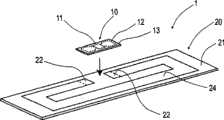
本例的内插器接合装置3如图1和图2所示,是一种用于将板状的芯片保持构件13上安装半导体芯片11而构成并具有从该半导体芯片11延伸设置的作为连接端子的内插器侧端子12的内插器10,与由板状的基底构件21构成、在其表面设置了基底侧端子22的基底电路板20接合的设备。The
该内插器接合装置3具有:在内插器侧端子12与基底侧端子22对置的状态下,对层叠了内插器10的基底电路板20进行保持的冲压砧31;和 构成为相对冲压砧31进行相对运动的接合头32。This
这里,该接合头32具有按照与内插器10的背面抵接的方式形成的加压面320而成,该加压面320构成为:根据接合头32相对冲压砧31的相对运动扫描内插器10的背面,至少相对基底电路板20加压内插器侧端子12的整个面。Here, the
下面,对该内容进行详细说明。Hereinafter, this content will be described in detail.
首先,在本例中制作的电子部件1如图2所示,是非接触ID用的RF-ID(Radio-Frequency IDentification)媒体(下面适当记载为RF-ID媒体1)。该RF-ID媒体1将作为半导体芯片11安装了RF-ID用的IC芯片(下面适当记载为IC芯片11)的内插器10、和作为上述基底电路板20设置了天线图案24的天线板(下面适当记载为天线板20)进行层叠接合而成。First, the electronic component 1 manufactured in this example is an RF-ID (Radio-Frequency IDentification) medium for non-contact ID as shown in FIG. 2 (hereinafter referred to as RF-ID medium 1 as appropriate). This RF-ID medium 1 includes an
如图2所示,内插器10是在由PSF构成的厚度200μm的板状芯片保持构件13的表面安装了IC芯片11的构件。在该芯片保持构件13的表面,设置有与IC芯片11的电极焊点(省略图示)电连接的导电焊点(省略图示)、和从该导电焊点延伸设置的内插器侧端子12。其中,在本例中,导电焊点及内插器侧端子12由导电性墨形成。As shown in FIG. 2 , the
另外,作为芯片保持构件13的材质可以替代本例的PSF,而采用PC、加工纸等。而且,为了保护导电焊点和电极焊点的电连接部位,可以利用底部填充材料或封装材料等。并且,作为芯片保持构件13的内插器侧端子12等的形成方法,可替代本例的印刷导电性墨的方法,而采用铜蚀刻、分配(dispense)、金属箔贴附、金属的直接蒸镀、金属蒸镀膜转印、导电高分子层形成等方法。In addition, as the material of the
天线板20如图2所示,在由材质PET构成的厚度100μm的热塑性基底构件21的表面,设置有由导电性墨构成的天线图案24。该天线图案24呈在一处被切断的近似环状。而且,在天线图案24的构成上述一处的两端部,设置有与内插器侧端子12电连接的基底侧端子22。As shown in FIG. 2 , the
另外,和形成于上述芯片保持构件13的内插器侧端子12同样,可替代由导电性墨构成的天线图案24,采用通过铜蚀刻箔、分配、金属箔贴附、金属的直接蒸镀、金属蒸镀膜转印、导电高分子层形成等方法形成的天线 图案24。而且,作为基底构件21的材质,除了本例的PET之外,可以使用PET-G、PC、PP、尼龙、纸等。进而,作为导电性墨的墨材料可使用银、石墨、氯化银、铜、镍等。In addition, similar to the interposer-
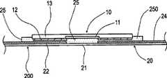
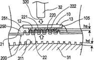
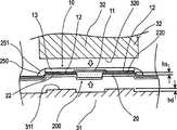
接着,对本例的内插器接合装置3进行说明。本例的内插器接合装置3如图3和图4所示,由大致呈圆柱形状的辊形状的冲压砧31、和相对冲压砧31的外表面设置规定间隙G并具有对置的加压面320的接合头32构成。Next, the
冲压砧31如图1、图3及图4所示,构成为将配置了内插器10的连续板状的连续天线板200,保持于近似圆柱形状的外表面。该连续天线板200由连续板状的基底构件21构成,在其表面连续地设置有天线图案24。本例的内插器接合装置3构成为:使用在各天线图案24上配置了内插器10的连续天线板200,连续地实施内插器10的接合。As shown in FIG. 1 , FIG. 3 and FIG. 4 , the
冲压砧31如图1、图3、图4及图7所示,构成为按照沿着其轴心方向配置一对基底侧端子22的方式保持上述连续天线板200。而且,在冲压砧31的外周面对应于各基底侧端子22设置有两列凸形成部310。该凸形成部310形成为遍布冲压砧31的整个外周而延伸设置的近似圆环状。如图9所示,凸形成部310被设置成与连续天线板200的各基底侧端子22对置。As shown in FIGS. 1 , 3 , 4 and 7 , the stamping
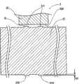
凸形成部310如图3及图4所示,通过连续地设置按照与轴心方向近似平行的方式延伸设置的条纹状突出部311而成。各突出部311朝向冲压砧31的外周侧突出。在本例中,按照数个突出部311相对各基底侧端子22对置的方式,设定其形成间距(参照图8)。而且,在本例中,设上述突出部311的突出高度hd为400μm。As shown in FIGS. 3 and 4 , the convex forming
并且,本例的冲压砧31具有未图示的加热器。而且,构成为可以通过该加热器所产生的热量加热各突出部311。另外,在本例的内插器接合装置3中,通过加热后的突出部311对连续天线板200进行加压。由此,可以使构成连续天线板200的由热塑性材料形成的基底构件21容易、且形状精度高地突出变形。Moreover, the
接合头32如图3及图4所示,像上述那样构成为相对于冲压砧31的各突出部311的突出表面所构成的最外周表面设置230μm的间隙G而对置。并且,本例的接合头32具有未图示的加振单元。该加振单元构成为对接合头32的加压面320作用超声波振动。其中,在本例的情况下,优选将上述间隙G设定为220~250μm。As shown in FIGS. 3 and 4 , the
另外,加压面320被实施作为表面处理的金刚石涂敷处理,来抑制与内插器10的背面的摩擦。替代该处理,对加压面实施特氟隆(R)涂敷等表面处理,或在加压面320的表面配置由碳化钨构成的超硬芯片也是有效的。或者,也可以在接合头32的前端设置旋转辊,将该旋转辊的外周面作为加压面。In addition, the
接着,对使用了本例的内插器接合装置3的RF-ID媒体1的制作顺序进行说明。当制作将内插器10与天线板20接合的RF-ID媒体1时,如图5所示,首先,通过在连续板状的基底构件21的表面形成天线图案24,来准备上述连续天线板200。然后,利用该连续天线板200,至少对基底侧端子22的表面实施如下工序:设置具有电绝缘性的绝缘性粘结剂250的粘结剂配置层25的粘结剂涂敷工序;配置内插器10的内插器配置工序;利用上述内插器接合装置3来接合内插器10的接合工序。然后,从接合了内插器10的连续天线板200切下各个RF-ID媒体1。Next, the procedure for producing the RF-ID medium 1 using the
在粘结剂涂敷工序中如图5所示,对连续天线板200的表面中、包含一对基底侧端子22的区域涂敷绝缘性粘结剂250,并设置了粘结剂配置层25。在本例中,按照包含内插器10的配置区域的方式,设置了厚度40~80μm的粘结剂配置层25。其中,本例中作为该绝缘性粘结剂250,使用了具有热塑性且为湿气固化型的热熔性粘结剂(hot melt)(3M公司制造的型号TE-031)。In the adhesive application process, as shown in FIG. 5 , an insulating
另外,作为绝缘性粘结剂250除了上述之外,还可以利用环氧系粘结剂、丙烯酸系粘结剂、弹性粘接剂、聚氨酯系粘结剂等。此外,也可以替代湿气固化型的绝缘性粘结剂250,使用热固化型、紫外线固化型、电子束固化型等反应型的粘结剂。In addition, as the insulating
接着,在内插器配置工序中如图5及图6所示,按照基底侧端子22与内插器侧端子12分别对置的方式,在连续天线板200的表面配置内插器10。这里,本例中如上所述,包含内插器10的配置区域而设置了上述粘结剂配置层25。因此,内插器10以其整个表面夹设绝缘性粘接层25 而与天线板20对置。Next, in the interposer arrangement step, as shown in FIGS. 5 and 6 , the
接着,如图7~图9所示,使用本例的内插器接合装置3,实施相对连续天线板200加压接合内插器10的接合工序。如上所述,内插器接合装置3的冲压砧31具有按照与各基底侧端子22的背面对置的方式条纹状连续地设置的突出部311。而且,通过本例的突出高度hd=400μm的突出部311,可以在基底侧端子22上形成突出高度hs=约100μm的突出变形部220。其中,作为突出部311的突出高度hd优选设为100~800μm。该情况下,能够从邻接的突出部311的间隙排出有可能从内插器10与连续天线板200之间流出的绝缘性粘结剂250。Next, as shown in FIGS. 7 to 9 , using the
而且,在本例中,使将加压面的表面温度维持为200℃的冲压砧31旋转,将冲压砧31通过连续天线板200保持的内插器10,连续地向接合头32所成的间隙G搬送。如上所述,在本例中,相对于构成连续天线板200的100μm厚的基底构件21、和构成内插器10的200μm厚的芯片保持构件13的组合,将冲压砧31与接合头32的间隙G设定为230μm。因此,如果在连续天线板200的表面配置的内插器10通过上述的间隙,则可以相对连续天线板200加压内插器10。本例的内插器接合装置3利用在这里产生的加压力,牢固地接合内插器10。Furthermore, in this example, the
根据具备设置了凸形成部310的冲压砧31与接合头32的组合的本例的内插器接合装置3,可以通过突出部311使天线板20中的各基底侧端子22的一部分突出变形。即,如图8及图9所示,可以与在冲压砧31的加压表面以条纹状设置的突出部311对应,在各基底侧端子22上形成条纹状的突出变形部220。而且,基底侧端子22与内插器侧端子12经由该条纹状的突出变形部220直接接触,在该突出变形部220以外的部分,在二者之间形成间隙222。According to the
因此,在该突出变形部220与内插器侧端子12之间流出绝缘性粘结剂250,使得突出变形部220被压接于内插器侧端子12。由此,能够可靠性高地实现内插器侧端子12与基底侧端子22的电连接。另一方面,在各基底侧端子22中的除了突出变形部220之外的非突出部221与对置的内插器侧端子12的间隙222中,完全不流出绝缘性粘结剂250,适量的绝缘性粘结剂250原样地残留。因此,通过残留于该间隙的绝缘性粘结剂250, 能够可靠性高地实现内插器侧端子12与基底侧端子22之间的粘结接合,即物理连接。Therefore, the insulating
并且,本例中,在包含内插器10的配置区域的区域设置了粘结剂配置层25。因此,内插器10以其几乎整个表面通过绝缘性粘结剂250与连续天线板200对置。其结果,内插器10被牢固粘结于连续天线板200。Furthermore, in this example, an
另外,如果使内插器10和天线板20抵接而进行加压,则剩余的绝缘性粘结剂250会迂回附着于内插器10的外周侧面。结果,在内插器10的外周侧面与连续天线板200之间,形成由绝缘性粘结剂250构成的倾斜状倾斜面251。由此,除了内插器10的表面之外,内插器10的外周侧面105也成为粘结面,使得内插器10非常牢固地接合于连续天线板200。In addition, when the
并且,本例的内插器接合装置3,在与由热塑性材料构成的基底构件21抵接的冲压砧31中具备加热器。因此,通过一边使用该冲压砧31加热连续天线板200,一边实施上述接合工序,利用冲压砧31的突出部311能够效率良好且形状精度高地形成上述突出变形部220。而且,可以相对内插器侧端子12热压接突出变形部220,从而能够提高电连接可靠性。Furthermore, the
这里,本例中所使用的绝缘性粘结剂250具有热塑性。因此,如果通过加热器加热绝缘性粘结剂250,则可提高其流动性。因此,可以使绝缘性粘结剂250高可靠性地从基底侧端子22的突出变形部220、与内插器侧端子12之间流出,从而能够可靠性良好地实现二者之间的电连接。Here, the insulating
而且,上述内插器接合装置3如上所述,具备用于对接合头32进行超声波加振的加振单元。因此,在内插器侧端子12与基底侧端子22直接接触的位置,可通过超声波接合熔接二者,从而能够进一步提高电连接可靠性。如果组合热压接和基于超声波接合的熔接来接合内插器侧端子12和基底侧端子22,则在长期使用RF-ID媒体1的使用期间,能够高稳定性维持两者间的优越的电连接状态。Furthermore, the above-mentioned
并且,本例中所使用的绝缘性粘结剂250是湿气固化型的反应型粘结剂。因此,当实施了上述加压冲压工序之后,在所制作的RF-ID媒体1的保管过程中等,可以完全接近内插器10的接合状态。In addition, the insulating
另外,作为在冲压砧31的加压表面设置的突出部311的形状,可替代本例的条纹状,形成块状、分布状、十字状、梳形状等各种形状的突出 部311。并且,作为凸形成部310,也可以将在冲压砧31的外周面沿其周方向延伸设置的近似圆环状的突出部311沿轴心方向并列配置。In addition, as the shape of the protruding
例如,作为块状的突出部311如图10所示,可替代本例的条纹状的一个突出部311(由符号DL表示的形状),在一条直线上设置大致等间隔配置的5个块状的突出形状。该情况下,这些各突出形状分别构成各个突出部311。此时,作为这些突出部311的整体所构成的凸形成部310的配置形状,可以与本例的凸形成部310(参照图3及图4)近似相同。另外,作为各突出部311的截面形状例如可以为400μm(该图中由Wt表示的尺寸)×400μm的正方形。而且,在凸形成部310中,可以将邻接的突出部311的间隔Wh设定为400μm。这里,作为各突出部311的突出倾斜角D优选设定为5度~15度。For example, as shown in FIG. 10, as the block-shaped protruding
此外,本例中按照包含内插器10的配置区域的方式设置了粘结剂配置层25。也可以替代该作法,比内插器10的配置区域小地限定于其内周部来设置粘结剂配置层25。并且,也可以对应于各基底侧端子22,分别独立地形成粘结剂配置层25。In addition, in this example, the
本例的内插器10的接合方法不限定于RF-ID媒体1的制造,在使用了内插器10的各种电子部件的制作中都是有效的。例如,可以在FPC(挠性印刷基板)、纸制计算机(paper computer)、即抛式电气制品等各种电子部件的制造工序中灵活运用。The bonding method of the
(实施例2)(Example 2)
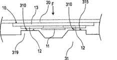
本例是以实施例1的内插器接合装置3为基础,主要变更了接合头32的加压面320及冲压砧31的凸形成部310的形状的例子。参照图11~图16对该内容进行说明。This example is based on the
在本例的内插器接合装置3中如图11所示,接合头32与天线板20抵接,冲压砧31与内插器10抵接。In the
本例的接合头32如图11及图12所示,具有与冲压砧31的弯曲状的外周面对应地形成为弯曲凹状的加压面320。该加压面320在冲压砧31的周方向上的尺寸比内插器10宽。因此,在本例的内插器接合装置3中,能够以冲压砧31搬送内插器10的规定时间通过加压面320同时加压内插器侧端子12的整个面。As shown in FIGS. 11 and 12 , the
如图12所示,在加压面320中,在冲压砧31的轴向的大致中央部,设置有沿上述周方向延伸设置的凹部328。因此,根据该加压面320,对内插器10的IC芯片11作用过大的负荷的可能性小。另外,在加压面320的缘部中,优选冲压砧31的旋转上游侧的缘部329将其角形状预先形成为凸曲面状。该情况下,能够顺畅地将内插器10及天线板20送入加压面320侧。As shown in FIG. 12 , on the
如图13~图15所示,本例的冲压砧31的各凸形成部310,分别形成在沿以轴心为中心的旋转方向延伸设置的大径的基座部319的外周面。各凸形成部310分别具有两列沿周方向排列的突出部315。另外,在图13中省略了接合头32并且由虚线表示了天线板20及内插器10。As shown in FIGS. 13 to 15 , the convex forming
本例的突出部315如图15所示,是在前端设置了平面部的近似四角锥状的形状。作为突出部315的形状,除了本例的四角锥状之外,可以形成为三角锥状或圆锥状等各种形状。As shown in FIG. 15 , the protruding
另外,在本例的内插器接合装置3中如图16所示,也能够在使接合头32与内插器10抵接、冲压砧31与天线板20抵接的状态下,接合内插器10。In addition, in the
Claims (9)
Translated fromChineseApplications Claiming Priority (5)
| Application Number | Priority Date | Filing Date | Title |
|---|---|---|---|
| JP2004351258 | 2004-12-03 | ||
| JP2004350841 | 2004-12-03 | ||
| JP350841/2004 | 2004-12-03 | ||
| JP351258/2004 | 2004-12-03 | ||
| PCT/JP2005/022220WO2006059732A1 (en) | 2004-12-03 | 2005-12-03 | Interposer bonding device |
Related Child Applications (1)
| Application Number | Title | Priority Date | Filing Date |
|---|---|---|---|
| CN2008101693806ADivisionCN101383022B (en) | 2004-12-03 | 2005-12-03 | Electronic component |
Publications (2)
| Publication Number | Publication Date |
|---|---|
| CN101073296A CN101073296A (en) | 2007-11-14 |
| CN101073296Btrue CN101073296B (en) | 2011-07-06 |
Family
ID=38899521
Family Applications (2)
| Application Number | Title | Priority Date | Filing Date |
|---|---|---|---|
| CN2005800416497AActiveCN101073296B (en) | 2004-12-03 | 2005-12-03 | Interposer Engagement Device |
| CN2008101693806AActiveCN101383022B (en) | 2004-12-03 | 2005-12-03 | Electronic component |
Family Applications After (1)
| Application Number | Title | Priority Date | Filing Date |
|---|---|---|---|
| CN2008101693806AActiveCN101383022B (en) | 2004-12-03 | 2005-12-03 | Electronic component |
Country Status (1)
| Country | Link |
|---|---|
| CN (2) | CN101073296B (en) |
Families Citing this family (2)
| Publication number | Priority date | Publication date | Assignee | Title |
|---|---|---|---|---|
| EP3244801B1 (en)* | 2015-01-13 | 2019-08-14 | Koninklijke Philips N.V. | Interposer electrical interconnect with spring |
| CN109399114B (en)* | 2018-12-11 | 2023-12-29 | 宁波隆威婴儿用品有限公司 | Comb body grain planting machine |
Citations (4)
| Publication number | Priority date | Publication date | Assignee | Title |
|---|---|---|---|---|
| US6126456A (en)* | 1998-03-04 | 2000-10-03 | International Business Machines Corporation | Solder column tip compliancy modification for use in a BGA socket connector |
| CN1331820A (en)* | 1998-12-21 | 2002-01-16 | 格姆普拉斯公司 | Method for producing a contactless chip card |
| JP2003168099A (en)* | 2001-11-30 | 2003-06-13 | Oji Paper Co Ltd | IC chip package manufacturing equipment |
| JP2004265920A (en)* | 2003-02-07 | 2004-09-24 | Hallys Corp | Piece transfer equipment capable of carrying out random periodic transfer speed change |
Family Cites Families (2)
| Publication number | Priority date | Publication date | Assignee | Title |
|---|---|---|---|---|
| US5591298A (en)* | 1988-01-19 | 1997-01-07 | Kimberly-Clark Corporation | Machine for ultrasonic bonding |
| US5342460A (en)* | 1989-06-13 | 1994-08-30 | Matsushita Electric Industrial Co., Ltd. | Outer lead bonding apparatus |
- 2005
- 2005-12-03CNCN2005800416497Apatent/CN101073296B/enactiveActive
- 2005-12-03CNCN2008101693806Apatent/CN101383022B/enactiveActive
Patent Citations (4)
| Publication number | Priority date | Publication date | Assignee | Title |
|---|---|---|---|---|
| US6126456A (en)* | 1998-03-04 | 2000-10-03 | International Business Machines Corporation | Solder column tip compliancy modification for use in a BGA socket connector |
| CN1331820A (en)* | 1998-12-21 | 2002-01-16 | 格姆普拉斯公司 | Method for producing a contactless chip card |
| JP2003168099A (en)* | 2001-11-30 | 2003-06-13 | Oji Paper Co Ltd | IC chip package manufacturing equipment |
| JP2004265920A (en)* | 2003-02-07 | 2004-09-24 | Hallys Corp | Piece transfer equipment capable of carrying out random periodic transfer speed change |
Also Published As
| Publication number | Publication date |
|---|---|
| CN101073296A (en) | 2007-11-14 |
| CN101383022B (en) | 2012-08-22 |
| CN101383022A (en) | 2009-03-11 |
Similar Documents
| Publication | Publication Date | Title |
|---|---|---|
| JP5036541B2 (en) | Electronic component and method of manufacturing the electronic component | |
| US6882545B2 (en) | Noncontact ID card and method of manufacturing the same | |
| JP4479209B2 (en) | Electronic circuit device, method for manufacturing the same, and apparatus for manufacturing electronic circuit device | |
| JP3928682B2 (en) | Wiring board bonded body, wiring board bonding method, data carrier manufacturing method, and electronic component module mounting apparatus | |
| JP4091096B2 (en) | Interposer joining device | |
| CN101073296B (en) | Interposer Engagement Device | |
| JP4628067B2 (en) | Interposer joining method and electronic component. | |
| CN101073297A (en) | Electronic component production method and electronic component production equipment | |
| JP4917119B2 (en) | Wiring board front and back conduction method | |
| JP6562750B2 (en) | Electronic component, connection body, manufacturing method of connection body, connection method of electronic component, cushioning material | |
| JP5171405B2 (en) | Interposer joining method | |
| CN105430901B (en) | Electronic component and connection method thereof, connection body and manufacturing method thereof, and buffer material | |
| JP3752836B2 (en) | Bonding method for electronic components | |
| JP6719529B2 (en) | Electronic component, connecting body, manufacturing method of connecting body, and connecting method of electronic component | |
| JP5437623B2 (en) | IC tag | |
| JP2008521105A (en) | Method for connecting a bridge module to a substrate and a multi-layer transponder | |
| JP2004086852A (en) | Non-contact id card or the like, and its manufacturing method | |
| JP5548059B2 (en) | Circuit element | |
| JP3894541B2 (en) | IC chip mounting interposer manufacturing method and IC chip mounting media manufacturing method using the same | |
| KR20220103423A (en) | Display device and manufacturing method thereof | |
| JP2020202277A (en) | Bonding head and semiconductor chip mounting method | |
| HK1220074B (en) | Electronic component and its connection method, connector and its manufacturing method, and a cushioning material | |
| JP2002304607A (en) | Method for manufacturing non-contact IC inlet | |
| JP2006092006A (en) | Non-contact communication equipment and method for manufacturing the same | |
| JP2002050734A (en) | Method of manufacturing semiconductor module |
Legal Events
| Date | Code | Title | Description |
|---|---|---|---|
| C06 | Publication | ||
| PB01 | Publication | ||
| C10 | Entry into substantive examination | ||
| SE01 | Entry into force of request for substantive examination | ||
| C14 | Grant of patent or utility model | ||
| GR01 | Patent grant |