CN101069391A - Streaming Storage Controller - Google Patents
Streaming Storage ControllerDownload PDFInfo
- Publication number
- CN101069391A CN101069391ACNA2005800412551ACN200580041255ACN101069391ACN 101069391 ACN101069391 ACN 101069391ACN A2005800412551 ACNA2005800412551 ACN A2005800412551ACN 200580041255 ACN200580041255 ACN 200580041255ACN 101069391 ACN101069391 ACN 101069391A
- Authority
- CN
- China
- Prior art keywords
- memory
- network
- mem
- interface
- streaming
- Prior art date
- Legal status (The legal status is an assumption and is not a legal conclusion. Google has not performed a legal analysis and makes no representation as to the accuracy of the status listed.)
- Pending
Links
Images


Classifications
- H—ELECTRICITY
- H04—ELECTRIC COMMUNICATION TECHNIQUE
- H04L—TRANSMISSION OF DIGITAL INFORMATION, e.g. TELEGRAPHIC COMMUNICATION
- H04L49/00—Packet switching elements
- H04L49/90—Buffering arrangements
- H04L49/9063—Intermediate storage in different physical parts of a node or terminal
- G—PHYSICS
- G06—COMPUTING OR CALCULATING; COUNTING
- G06F—ELECTRIC DIGITAL DATA PROCESSING
- G06F13/00—Interconnection of, or transfer of information or other signals between, memories, input/output devices or central processing units
- G06F13/14—Handling requests for interconnection or transfer
- G06F13/16—Handling requests for interconnection or transfer for access to memory bus
- G06F13/1668—Details of memory controller
- G06F13/1673—Details of memory controller using buffers
- H—ELECTRICITY
- H04—ELECTRIC COMMUNICATION TECHNIQUE
- H04L—TRANSMISSION OF DIGITAL INFORMATION, e.g. TELEGRAPHIC COMMUNICATION
- H04L49/00—Packet switching elements
- H04L49/90—Buffering arrangements
Landscapes
- Engineering & Computer Science (AREA)
- Theoretical Computer Science (AREA)
- Computer Networks & Wireless Communication (AREA)
- Signal Processing (AREA)
- Physics & Mathematics (AREA)
- General Physics & Mathematics (AREA)
- General Engineering & Computer Science (AREA)
- Data Exchanges In Wide-Area Networks (AREA)
- Information Transfer Systems (AREA)
- Bus Control (AREA)
- Use Of Switch Circuits For Exchanges And Methods Of Control Of Multiplex Exchanges (AREA)
- Vehicle Body Suspensions (AREA)
- Magnetically Actuated Valves (AREA)
Abstract
Description
Translated fromChinese技术领域technical field
本发明涉及一种用于连接网络和存储器的存储控制器及其方法。The invention relates to a storage controller and method for connecting network and storage.
背景技术Background technique
先进的移动和便携式设备的复杂性增加了。这种设备更多要求的应用,其复杂性、灵活性以及可编程的需求增加了设备内部的数据交换。实现这些应用的设备经常由一些功能或处理模块(这里称为子系统)组成。这些子系统典型地作为独立的IC电路实现,每个子系统具有由本地处理器、总线以及存储器等组成的不同的内部结构。替代地,各种子系统可集成在一个集成电路上。在系统级,这些子系统通过顶层互连线路相互通信,此顶层互连线路经常以实时支持提供某些服务。作为子系统的示例,在移动电话结构中,其中我们可具有基带处理器、显示器、媒体处理器或存储元件。对于多媒体应用的支持,这些子系统以流式交换大多数数据。作为数据流的示例,提到了:媒体处理器从本地存储器中读出MP3编码音频文件中,并将译码后的流发送到扬声器。图1示出了这样一个通信的基本表征,此通信可描述成通过FIFO缓冲器B而连接的步骤P1-P4。这样的表征经常被称作Kahn处理网络。Kahn处理网络可以映射到如E.A.de Kock等人,“YAPI:Application modeling for signal processing systems”,在Proc.Of the37th Design Automation Conference中,Los Angeles,CA,2000年6月,第402-405页,IEEE,2000所描述的系统结构。在这样的结构中,处理被映射到子系统、存储器SMEM的FIFO缓冲器以及系统层互连IM上的通信。The complexity of advanced mobile and portable devices has increased. The more demanding applications of such devices, the complexity, flexibility and programmability requirements increase the data exchange within the device. Devices implementing these applications are often composed of some functional or processing modules (herein referred to as subsystems). These subsystems are typically implemented as separate IC circuits, each with a different internal structure consisting of a local processor, bus, and memory. Alternatively, various subsystems can be integrated on one integrated circuit. At the system level, these subsystems communicate with each other through a top-level interconnect, which often provides certain services in real-time support. As an example of a subsystem, in a mobile phone architecture, where we may have a baseband processor, a display, a media processor or a storage element. For the support of multimedia applications, these subsystems exchange most of the data in streams. As an example of a data stream, it is mentioned that a media processor reads an MP3 encoded audio file from a local memory, and sends the decoded stream to a speaker. Figure 1 shows the basic representation of such a communication, which can be described as steps P1-P4 connected through FIFO buffer B. Such representations are often referred to as Kahn processing networks. The Kahn processing network can be mapped to as in EAde Kock et al., "YAPI: Application modeling for signal processing systems", in Proc.Of the37th Design Automation Conference, Los Angeles, CA, June 2000, pp. 402-405, IEEE, 2000 describes the system structure. In such an architecture, processing is mapped to communications on subsystems, FIFO buffers of memory SMEM, and system layer interconnect IM.
缓冲对于有关处理之间的数据流的适当支持中是至关重要的。典型地,FIFO缓冲器被用于根据流式应用的(受限的)Kahn处理网络模型的流。随着可同时运行的多媒体应用数量的增加,处理的数量、实时流以及与相关联的FIFO数量也明显地增加。Buffering is critical in proper support for data flow between processes. Typically, FIFO buffers are used for streaming according to the (restricted) Kahn processing network model for streaming applications. As the number of concurrently running multimedia applications increases, the number of processes, real-time streams, and associated FIFOs also increases significantly.
存在两种关于存储器的使用和FIFO分配的流的最大实现。第一种是使用物理分布的存储器,其中FIFO缓冲器被分配在子系统的本地存储器中。第二种是使用物理以及逻辑上统一的存储器,其中所有的FIFO缓冲器都分配在一个共享的(经常是芯片外的)存储器中。这两种的组合也是可能的。There are two maximum implementations of flow with respect to memory usage and FIFO allocation. The first is to use physically distributed memory, where the FIFO buffers are allocated in the subsystem's local memory. The second is to use a physically and logically unified memory, where all FIFO buffers are allocated in a shared (often off-chip) memory. Combinations of the two are also possible.
FIFO缓冲器可在使用外部DRAM存储技术的共享存储器中实现。SDRAM和DDR-SDRAM是以低成本提供大容量外部存储器的技术,具有非常有吸引力的成本对硅面积比。FIFO buffers can be implemented in shared memory using external DRAM memory technology. SDRAM and DDR-SDRAM are technologies that provide large-capacity external memory at low cost, with a very attractive cost-to-silicon area ratio.
图2示出了具有共享存储器流式架构的芯片内系统的基本结构。处理单元C、S通过缓冲器B相互通信。处理单元C、S以及缓冲器中的每个都与接口单元IU相连,接口单元IU将其连接到互连装置IM。在共享存储器数据交换的情况下,此存储器还可用于其他目的。例如,该存储器还可用于代码执行或对于在主处理器上运行的程序的处理的动态存储分配。Figure 2 shows the basic structure of an on-chip system with a shared memory streaming architecture. The processing units C, S communicate with each other through the buffer B. Each of the processing units C, S and the buffer is connected to an interface unit IU which connects it to the interconnect means IM. In the case of shared memory data exchange, this memory can also be used for other purposes. For example, the memory may also be used for code execution or dynamic storage allocation for processing of programs running on the main processor.
这种包括互连装置、接口单元以及处理单元C、S和缓冲器B的通信结构或网络,可提供专用传输设施以及对应的架构,此架构提供某种数据传输保证(例如,对于数据的无错误传输的保证吞吐量或保证传输),或提供用于同步源和目的元件的同步服务,使得不会由于缓冲器下溢或溢出而丢失数据。如果由系统来执行实时流处理,并且需要对所有元件进行实时支持,这就变得重要了。This communication structure or network including interconnection devices, interface units, and processing units C, S and buffer B can provide dedicated transmission facilities and corresponding architectures, which provide certain data transmission guarantees (for example, for data without Guaranteed Throughput for Error Transmission or Guaranteed Delivery), or provide a synchronization service for synchronizing source and destination elements so that no data is lost due to buffer underflow or overflow. This becomes important if real-time stream processing is performed by the system and all elements need to be supported in real-time.
在许多芯片内系统(SoC)和微处理器系统内,背景存储器(DRAM)被用于数据的缓冲。当数据以流式通信,并在存储器中作为流来缓冲时,可使用预提取缓冲。这表示SDRAM的数据被预先读出,并保留在特定的(预提取)缓冲器中。当读出请求到达时,可从本地预提取缓冲器供应,通常在芯片内SRAM中实现,而无需另外由背景存储器(DRAM)引入的等待时间。这与已知的用于处理器的随机数据的高速缓存技术相似。对于流而言,数据的相邻(或者说成可预测的更好)地址用于预提取缓冲器中,而不是用在高速缓冲存储器的随机地址。更详细的描述,请参见J.L.Hennessy和D.A.Patterson的“Computer Architecture-A Quantitative Approach”。In many system-on-chip (SoC) and microprocessor systems, background memory (DRAM) is used for buffering of data. Prefetch buffering is used when data is communicated in a stream and buffered as a stream in memory. This means that data from SDRAM is pre-read and held in a specific (pre-fetch) buffer. When a read request arrives, it can be served from a local prefetch buffer, usually implemented in on-chip SRAM, without additional latency introduced by background memory (DRAM). This is similar to known caching techniques for random data in processors. For streams, contiguous (or better, predictable) addresses of data are used in the prefetch buffer instead of random addresses in the cache. For a more detailed description, see "Computer Architecture-A Quantitative Approach" by J.L. Hennessy and D.A. Patterson.
另一个方面,由于DRAM技术,突发地访问(读或写)DRAM更好。因此,经常实现回写式缓冲器,此回写式缓冲器将许多单一的数据访问聚集成一定大小的突发访问。一旦完成对于第一DRAM访问的初始处理,对于特定数量的访问(2/4/8全页),可没有任何延迟(1个周期内)地存储地址与前一个有特定关系(例如,下一个、前一个-根据总线策略)的并在存储器的每下一个周期被访问的每下一个数据字。因此,对存储器的流式访问,以相同的方式增加或减少对每个访问(例如,相邻地址)的地址时,总线访问在最小功率消耗上提供了最佳性能。对于有关DRAM存储器原理的更多信息,请参见Micron的128Mbit DDRRAM标准,http://download.micron.com/pdf/datasheets/dram/ddr/128MbDDRx4x8x16.pdf,通过引用包含其内容。On the other hand, due to DRAM technology, it is better to access (read or write) DRAM in bursts. Therefore, write-back buffers are often implemented that aggregate many single data accesses into burst accesses of a certain size. Once the initial processing for the first DRAM access is done, for a certain number of accesses (2/4/8 full pages), it is possible to store addresses with a specific relationship to the previous one (e.g., the next , previous - every next data word that is accessed every next cycle of the memory according to the bus policy. Thus, for streaming access to memory, bus accesses provide the best performance at minimum power consumption while increasing or decreasing addresses for each access (eg, adjacent addresses) in the same manner. For more information onthe principles of DRAM memory, see Micron's 128Mbit DDRRAM Standard,http://download.micron.com/pdf/datasheets/dram/ddr/128MbDDRx4x8x16.pdf , the contents of which are incorporated by reference.
直到现在,外部DRAM的控制器被设计为以基于总线的结构工作。总线只为数据传输服务、简单的媒体访问控制以及尽力而为的数据传输提供有限的服务。在这样的结构中,能够自动访问总线的单元也能访问共享存储器。此外,用在这种系统中的存储控制器只是最优化以执行大量低等待时间的读或写的访问模块,经常为处理器类似随机高速缓存的突发访问而被调节。作为控制器的低等待时间、高带宽以及高速度优化的副作用,外部DRAM的功率消耗相对较高。Until now, controllers for external DRAMs were designed to work in a bus-based structure. The bus provides only limited services for data transfer services, simple media access control, and best-effort data transfer. In such an architecture, units that can automatically access the bus can also access the shared memory. Furthermore, the memory controllers used in such systems are simply access modules optimized to perform a large number of low-latency reads or writes, often tuned for bursty accesses by the processor like random caches. As a side effect of the low latency, high bandwidth, and high speed optimization of the controller, the power consumption of the external DRAM is relatively high.
然而,上述的网络服务仅可用于网络内部。一旦与网络外部的任何组件发生数据交换,网络服务的保证无法得到满足。在共享存储结构内,所要缓冲的数据典型地通过物理统一的存储器来交换,这样数据需要传输到存储器以及从存储器传输,由此数据将违反网络所提供的服务,因为存储控制器或存储器本身都不支持任何网络服务。However, the above-mentioned network services are only available within the network. Network service guarantees cannot be satisfied once data is exchanged with any component outside the network. In a shared memory structure, the data to be buffered is typically exchanged through physically unified memory, so data needs to be transferred to and from memory, whereby the data will violate the services provided by the network, because neither the memory controller nor the memory itself No web services are supported.
发明内容Contents of the invention
本发明的目的是提供用于连接网络和存储器的存储控制器,以及用于连接网络和存储器的方法,此方法与存储器一起改善了网络和存储器之间的可预测的通信行为。It is an object of the present invention to provide a memory controller for connecting a network and a memory, and a method for connecting a network and a memory which, together with the memory, improves predictable communication behavior between the network and the memory.
此目的由根据权利要求1的存储控制器以及根据权利要求6的用于连接网络和存储器的方法来解决。This object is solved by a memory controller according to
提供了用于将存储器连接到网络的存储控制器。此存储控制器包括第一接口、流式存储单元以及第二接口。第一接口用于将存储控制器连接到网络,以接收和发送数据流。流式存储单元连接到第一接口,以控制网络和存储器之间的数据流。流式存储单元包括用于暂时存储至少部分数据流的缓冲器,以及用于管理缓冲器中的数据流的暂时存储的缓冲管理单元。第二接口连接到流式存储单元,以便将存储控制器连接到存储器来与存储器突发地交换数据。提供了流式存储单元以便在存储器上实现网络的网络服务。A storage controller for connecting the storage to the network is provided. The storage controller includes a first interface, a streaming storage unit and a second interface. The first interface is used to connect the storage controller to the network for receiving and sending data streams. The streaming storage unit is connected to the first interface to control data flow between the network and the storage. The stream storage unit includes a buffer for temporarily storing at least part of the data stream, and a buffer management unit for managing the temporary storage of the data stream in the buffer. The second interface is connected to the streaming storage unit to connect the storage controller to the memory to exchange data with the memory in bursts. A streaming storage unit is provided to implement network services of the network on the storage.
因此,使用这样的存储控制器,无法实现网络所提供的网络服务的存储器可与支持特定网络服务的通信网络结合在一起。换句话说,同样的服务可应用于网络内通信的数据或与存储子系统交换的数据。Therefore, using such a memory controller, a memory that cannot implement a network service provided by a network can be combined with a communication network that supports a specific network service. In other words, the same services apply to data communicated within the network or exchanged with storage subsystems.
根据本发明的一个方面,第一接口作为PCI-Express接口来实现,这样PCI-Express网络的属性和网络服务可由存储控制器来实现。According to one aspect of the present invention, the first interface is implemented as a PCI-Express interface, so that attributes and network services of the PCI-Express network can be implemented by the storage controller.
根据本发明的另一方面,存储器至少部分地组织成FIFO,并且流标识符与来自网络的每个数据流相关联。提供了流式存储单元,通过根据数据流的流标识符将特定数据流指向存储器中的特定FIFO,控制来自网络或到网络的数据流。此外,在访问存储器的不同数据流之间执行仲裁。第二接口被设置为与存储器交换相对粗粒度(coarse grain)数据流,以及与网络交换相对细粒度(fine grain)数据流。由于数据流的流标识符用于将数据流映射到存储器的FIFO上,从而实现了一个简单的寻址方案。According to another aspect of the invention, the memory is at least partially organized as a FIFO, and a flow identifier is associated with each data flow from the network. A streaming memory unit is provided to control the flow of data from or to the network by directing specific data streams to specific FIFOs in memory according to their stream identifiers. Additionally, arbitration is performed between different data streams accessing the memory. The second interface is configured to exchange relatively coarse grain data streams with the memory and relatively fine grain data streams with the network. A simple addressing scheme is implemented since the stream identifier of the data stream is used to map the data stream onto the FIFO of the memory.
根据本发明的另一个方面,网络作为PCI-Express接口来实现,此外PCI-Express ID为寻址目的用于网络。其后,第一接口作为PCI-Express接口来实现。流式存储单元将PCI-Express ID转换成FIFO存储地址,并且将FIFO存储地址转换成PCI-Express ID。因此,PCI-Express设备的寻址方案用于在存储器内对FIFO缓冲器进行寻址。According to another aspect of the invention, the network is implemented as a PCI-Express interface, in addition the PCI-Express ID is used for the network for addressing purposes. Thereafter, the first interface is implemented as a PCI-Express interface. The streaming storage unit converts the PCI-Express ID into a FIFO storage address, and converts the FIFO storage address into a PCI-Express ID. Therefore, the addressing scheme of the PCI-Express device is used to address the FIFO buffer within the memory.
本发明还涉及用于将存储器连接到网络的方法。通过用于将存储控制器连接到网络的第一接口(PI)接收并发送数据流。网络和存储器之间的数据流由流式存储单元(SMU)所控制。至少部分数据流暂时存储在缓冲器中。管理在缓冲器中的数据流的暂时存储。流式存储控制器通过第二接口连接到存储器,并且数据突发地与存储器进行交换,网络的网络服务在存储器上实现。The invention also relates to a method for connecting a memory to a network. Data streams are received and sent through a first interface (PI) for connecting the storage controller to the network. Data flow between the network and storage is controlled by a Streaming Memory Unit (SMU). At least part of the data stream is temporarily stored in a buffer. Manages temporary storage of data streams in buffers. The streaming storage controller is connected to the storage through the second interface, and data is exchanged with the storage in bursts, and network services of the network are implemented on the storage.
本发明涉及引入与共享存储器相关联的流式存储控制器的思想。流式存储控制器能够提供了与网络相同的服务。这样的服务可以是流控制、虚拟信道以及调整成网络带宽仲裁的存储器带宽仲裁。其后,如果数据为了在存储器中缓冲而离开网络,则网络所保证的这些服务还被存储控制器保证。因此,网络服务的完整性将从数据的源到目的得以保持。The present invention relates to the idea of introducing a streaming memory controller associated with a shared memory. The streaming storage controller can provide the same services as the network. Such services may be flow control, virtual channels, and memory bandwidth arbitration tuned to network bandwidth arbitration. Thereafter, these services guaranteed by the network are also guaranteed by the storage controller if the data leaves the network for buffering in memory. Therefore, the integrity of web services will be maintained from the source of the data to its destination.
本发明的其他方面从属于所附的权利要求。Other aspects of the invention are dependent on the appended claims.
附图说明Description of drawings
结合以下附图,并参考下面对实施例的描述,本发明的这些和其他方面将显而易见,并被阐明了:These and other aspects of the invention will be apparent from and elucidated with reference to the following description of the embodiments, taken in conjunction with the following drawings:
图1示出了Kahn处理网络的基本表征及其映射到共享存储结构上;Figure 1 shows the basic representation of the Kahn processing network and its mapping onto the shared memory structure;
图2示出了具有共享存储流架构的芯片内系统的基本结构;Figure 2 shows the basic structure of an on-chip system with a shared memory flow architecture;
图3示出了根据第一实施例的芯片内系统的方框图;Fig. 3 shows a block diagram of the system-on-chip according to the first embodiment;
图4示出了存储时钟被激活的状态下,SDRAM的逻辑结构;Fig. 4 shows the logical structure of SDRAM under the state that storage clock is activated;
图5示出了根据第二实施例的流式存储控制器SMC的方框图;Figure 5 shows a block diagram of a streaming storage controller SMC according to a second embodiment;
图6示出了流式存储控制器SMC的逻辑视图的方框图;Figure 6 shows a block diagram of a logical view of a streaming storage controller SMC;
图7示出了根据第三实施例的芯片内系统的结构的方框图;Fig. 7 shows a block diagram according to the structure of the system on chip of the third embodiment;
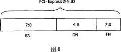
图8示出了PCI-Express网络内的ID格式;Figure 8 shows the ID format within the PCI-Express network;
图9示出了PCI-Express系统内的配置;Fig. 9 shows the configuration in the PCI-Express system;
图10示出了根据第四实施例的芯片内系统的方框图;FIG. 10 shows a block diagram of an on-chip system according to a fourth embodiment;
图11示出了图10的存储器内的内存分配的示例;Figure 11 shows an example of memory allocation within the memory of Figure 10;
图12示出了外部DDR-SDRAM的功率消耗对访问的突发大小以及最坏情况的延迟对网络包中的缓冲器大小的关系。Figure 12 shows the power consumption of the external DDR-SDRAM versus the burst size of the access and the worst case latency versus the buffer size in the network packet.
具体实施方式Detailed ways
图3示出了根据第一实施例的芯片内系统的方框图。消费者C和生产者P连接到PCI-Express网络PCIE。生产者和消费者P、C之间的通信是通过网络PCIE、流式存储控制器SMC执行到(外部)存储器MEM。(外部)存储器可作为DRAM或SDRAM来实现。由于生产者P和消费者C之间的通信为基于流的通信,为这个通信在外部存储器MEM中提供了FIFO缓冲器。Fig. 3 shows a block diagram of an on-chip system according to the first embodiment. Consumer C and producer P are connected to PCI-Express network PCIE. The communication between producers and consumers P, C is performed via the network PCIE, the streaming memory controller SMC to the (external) memory MEM. The (external) memory can be implemented as DRAM or SDRAM. Since the communication between producer P and consumer C is stream-based communication, a FIFO buffer is provided in the external memory MEM for this communication.
根据图3的流式存储控制器SMC有两个接口:一个对着PCIExpress结构(fabric),第二个对着DRAM存储器MEM。流式存储控制器SMC的PCI Express接口必须对从SDRAM存储器MEM所恢复出的数据执行通信量编整(traffic shaping),以遵守PCI Express的网络PCIE的通信量规则。在流式存储控制器SMC的另一个接口上,突发地执行对DRAM的访问,因为访问存储于DRAM的数据的这种模式对于功率消耗而言是最有利的。流式存储控制器SMC本身必须提供对于访问DRAM的不同流之间的智能仲裁,使得访问的吞吐量以及等待时间有所保证。此外,SMC还提供了对智能FIFO缓冲的管理功能。The streaming memory controller SMC according to FIG. 3 has two interfaces: one is facing the PCIExpress fabric, and the second is facing the DRAM memory MEM. The PCI Express interface of the streaming memory controller SMC must perform traffic shaping (traffic shaping) on the data recovered from the SDRAM memory MEM to comply with the traffic rules of the PCI Express network PCIE. On another interface of the streaming memory controller SMC, accesses to the DRAM are performed in bursts, since this mode of accessing data stored in the DRAM is the most favorable for power consumption. The streaming memory controller SMC itself must provide intelligent arbitration between different streams accessing DRAM, so that the access throughput and waiting time are guaranteed. In addition, SMC also provides the management function of the intelligent FIFO buffer.
在“PCI Express Base Specification,Revision 1.0”,PCI-SIG,2002年7月,www.pcisig.org中描述了PCI-Express网络的基本概念。The basic concepts of PCI-Express networking are described in "PCI Express Base Specification, Revision 1.0", PCI-SIG, July 2002,www.pcisig.org .
流式存储控制器的设计中考虑到的PCI Express网络的特征是:同步数据传输支持、流控制、以及专用寻址方案。此同步支持主要基于借助于虚拟信道VCs的同步和非同步通信量的分离。因此,像带宽和缓冲器这样的网络资源显然应被保留在特定流的交换结构中,使得不同虚拟信道VC的流之间没有冲突得以保证。此外,交换结构中的同步通信量,由调度(也就是进入控制(admission control)和服务分配(service discipline))来调节。The characteristics of the PCI Express network considered in the design of the streaming memory controller are: isochronous data transfer support, flow control, and a dedicated addressing scheme. This synchronization support is mainly based on the separation of synchronous and asynchronous traffic by means of virtual channels VCs. Therefore, network resources like bandwidth and buffers should obviously be reserved in the flow-specific switching fabric so that no conflicts between flows of different virtual channels VC are guaranteed. In addition, isochronous traffic in the switch fabric is regulated by scheduling (ie, admission control and service discipline).
在信任基础上执行流控制以保证,使得在网络PCIE中没有因缓冲器的下溢/溢出而丢失数据。当接收节点具有足够的空间来接收数据时,只允许每一网络节点通过网络连接将网络包发送到其他网络节点。每个虚拟信道VC包括专用流控制设施。因此,可通过链式PCI Express流控制来单独地实现每个虚拟信道VC的源和目的之间的同步。Flow control is performed on a trust basis to ensure that no data is lost due to buffer underflow/overflow in the network PCIE. Each network node is only allowed to send network packets to other network nodes over the network connection when the receiving node has enough space to receive the data. Each virtual channel VC includes dedicated flow control facilities. Therefore, synchronization between the source and destination of each virtual channel VC can be achieved individually through chained PCI Express flow control.
PCI Express寻址方案典型地使用32或64位存储地址。由于没有显式的存储地址可用,设备和功能IDs(即流IDs)可用于区别不同的流。存储控制器SMC本身将产生/将流IDs转换成实际的存储地址。PCI Express addressing schemes typically use 32 or 64 bit memory addresses. Since no explicit memory address is available, device and function IDs (ie stream IDs) can be used to distinguish different streams. The storage controller SMC itself will generate/translate the stream IDs into actual storage addresses.
为了进一步简化寻址方案,将虚拟信道VC的ID用作流标识符。由于PCI Express允许多达8个的虚拟信道VCs,其中一半可用于识别输入流,而另一半可用于识别从外部存储器输出的流。因此,可通过存储控制器SMC访问存储器的流的最大数量被限制为8。请注意,这样的限制是由于PCI Express允许不同VCs的流之间的仲裁,而不是同一虚拟信道VC内部的流之间的仲裁。然而,这样的限制仅专用于基于PCI Express的系统,而对于本发明的概念并非基本的。To further simplify the addressing scheme, the ID of the virtual channel VC is used as the flow identifier. Since PCI Express allows up to 8 virtual channel VCs, half of them can be used to identify the input stream, while the other half can be used to identify the output stream from the external memory. Therefore, the maximum number of streams that can access memory through the memory controller SMC is limited to 8. Note that this limitation is due to the fact that PCI Express allows arbitration between streams of different VCs, not between streams within the same virtual channel VC. However, such limitations are only specific to PCI Express-based systems and are not fundamental to the concepts of the present invention.
总的来说,存储控制器SMC的PCI Express接口由全PCI Express接口组成,另外还有一些对于地址翻译和流识别必要的逻辑。In general, the PCI Express interface of the storage controller SMC consists of a full PCI Express interface, plus some logic necessary for address translation and flow identification.
在第一个实施例中,使用了(DDR)SDRAM。作为示例,可参见如Micron的128-Mbit DDRRAM规范所描述的Micron’s 128-MbitDDR-SDRAM,使用http://download.micron.com/pdf/datasheets/dram/ddr/128MbDDRx4x8x16.pdf。这样的技术是优选的,因为它提供了期望的功率消耗和时序性能。然而,此设计是以参数表示的,并且存储控制器SMC可配置为也与单速率的存储器工作。由于DDR-SDRAM的性能与SDRAM相似(除了数据线的时序),则可用SDRAM的概念来解释基本要素。In the first embodiment, (DDR) SDRAM is used. Asan example, see Micron's 128-Mbit DDR-SDRAM as described in Micron's 128-Mbit DDRRAM specification, usinghttp://download.micron.com/pdf/datasheets/dram/ddr/128MbDDRx4x8x16.pdf . Such a technique is preferred because it provides desirable power consumption and timing performance. However, the design is parametric and the memory controller SMC can be configured to also work with single-rate memory. Since the performance of DDR-SDRAM is similar to that of SDRAM (except for the timing of data lines), the concept of SDRAM can be used to explain the basic elements.
PCI Express网络PCIE提供了网络服务,例如通过在实时流所经过的设备中独占资源/带宽预留,来保证实时数据传输。由标准控制器所支持的外部DRAM在中间没有任何智能存储控制器的情况下连接到PCI Express结构时,由PCI Express典型提供的带宽和延迟保证无法由存储器来满足,因为它无法给出任何保证,并作为对输入通信量的“从”。PCI Express network PCIE provides network services, such as guaranteeing real-time data transmission by exclusive resource/bandwidth reservation in the devices through which the real-time stream passes. When external DRAM backed by a standard controller is connected to the PCI Express fabric without any smart memory controller in between, the bandwidth and latency guarantees typically provided by PCI Express cannot be met by the memory as it cannot give any guarantees , and acts as a "slave" to incoming traffic.
标准的存储控制器的设计集中在最小可能的等待时间上传送最大可能的带宽。这样的方法适于处理器数据和指令(高速缓存)访问,而不适于同步通信量。为了能够提供外部DRAM所扩展的PCI Express网络的可预测的性能,需要能保证流的外部存储器的可预测性能的流式存储控制器。此外,我们旨在设计不仅能保证吞吐量和等待时间而且可以在访问这个DRAM的同时减少功率消耗的存储控制器。Standard memory controller designs focus on delivering the maximum possible bandwidth with the minimum possible latency. Such an approach is suitable for processor data and instruction (cache) accesses, not for isochronous traffic. To be able to provide the predictable performance of a PCI Express network extended by external DRAM, a streaming memory controller that guarantees the predictable performance of streaming external memory is required. Furthermore, we aim to design memory controllers that not only guarantee throughput and latency but also reduce power consumption while accessing this DRAM.
图4示出了存储器时钟被激活状态下的SDRAM的逻辑结构,即存储器处于上电模式之一。SDRAM包括逻辑单元L、存储阵列AR、以及数据行DR。当该时钟被禁止时,存储器处于低功率状态(下电模式)。FIG. 4 shows the logical structure of the SDRAM in the state where the memory clock is activated, that is, the memory is in one of the power-on modes. SDRAM includes a logic unit L, a storage array AR, and data rows DR. When this clock is disabled, the memory is in a low power state (power down mode).
应用于存储器的典型的命令是激活ACT、预充电PRE、读/写RD/WR、以及更新。激活命令负责:在充电之后,体(bank)和行地址被选择,并且数据行(经常称作页)被转移到读出放大器。数据保留在读出放大器中,直到预充电命令将数据恢复到阵列中合适的单元。当数据在读出放大器SAM中可用时,存储器被认为处于激活状态。这期间状态读和写可发生。在预充电命令之后,存储器被认为处于预充电状态,在预充电状态所有数据都存储在单元阵列中。存储器操作的另一个应注意的方面是更新。SDRAM的存储单元通过使用小的电容器来存储数据,并且这些存储单元必须有规律地再次充电以保证数据的完整性。上电时,由存储控制器下命令使SDRAM存储器执行更新。下电时,SDRAM处于自更新模式(即没有时钟使能),并且存储器执行自身的更新。这个状态消耗非常少的电力。存储器从自更新模式跳出至其中数据可被断言为读或写的状态比其他模式花费更多的时间(例如,具体地对于DDR-SDRAM,200个时钟周期)。Typical commands applied to memory are activate ACT, precharge PRE, read/write RD/WR, and update. The activate command is responsible for: after charging, the bank and row addresses are selected and the row of data (often called page) is transferred to the sense amplifiers. Data remains in the sense amplifiers until a precharge command restores the data to the appropriate cells in the array. A memory is considered active when data is available in the sense amplifier SAM. Status reads and writes can occur during this time. After a precharge command, the memory is considered to be in a precharge state where all data is stored in the cell array. Another aspect of memory manipulation that should be kept in mind is updates. SDRAM memory cells store data by using small capacitors, and these memory cells must be recharged regularly to ensure data integrity. When the power is turned on, the SDRAM memory is updated by ordering the memory controller. When powered down, SDRAM is in self-refresh mode (ie, no clocks are enabled), and the memory performs its own update. This state consumes very little power. It takes more time for the memory to transition from self-refresh mode to a state where data can be asserted as read or written than other modes (eg, 200 clock cycles specifically for DDR-SDRAM).
存储器的时序和功率管理对于必须提供特定带宽、等待时间以及功率保证的存储控制器SMC的适当设计是很重要的。从被激活的SDRAM中读全页(等于1Kbyte),对于1次读取的突发长度可能耗费2560个时钟周期(~19.2us),8次读取的突发长度为768个时钟周期(~5.8us),以及全页突发仅为516个时钟周期(~3.9us)。这些值是基于如“Micron’s 128-Mbit DDRRAM规范,http://download.micron.com/pdf/datasheets/dram/ddr/128MbDDRx4x8x16.pdf”所描述的具有7.5ns时钟周期的特定128-Mbit DDR-SDRAM。The timing and power management of the memory is important to the proper design of the memory controller SMC which must provide certain bandwidth, latency and power guarantees. Reading a full page (equal to 1Kbyte) from an activated SDRAM may take 2560 clock cycles (~19.2us) for a burst length of 1 read, and 768 clock cycles for a burst length of 8 reads (~ 5.8us), and a full page burst of only 516 clock cycles (~3.9us). These values are based ona specific 128-Mbit DDR with a 7.5ns clock period as described in "Micron's 128-Mbit DDRRAM Specification,http://download.micron.com/pdf/datasheets/dram/ddr/128MbDDRx4x8x16.pdf " -SDRAM.
图5示出了根据第二实施例的流式存储控制SMC的方框图。流式控制存储器SMC包括PCI-Express接口PI、流式存储单元SMU以及作为到(外部)SDRAM存储器的接口的另外接口MI。流式存储单元SMU包括缓冲管理单元BMU、可作为SRAM存储器来实现的缓冲器B、以及仲裁器ARB。在SRAM中实现缓冲的流式存储单元SMU,与缓冲管理器一起用于对通过PCI-Express接口到SDRAM的访问进行缓冲。缓冲管理单元BMU用于对从PCI-Express接口对SDRAM的读或写访问起作用,以便管理缓冲器(更新指示字寄存器),并且中继从缓冲器(SRAM)到SDRAM或从SDRAM到缓冲器(SRAM)的数据。具体地,缓冲管理单元BMU可包括FIFO管理器和流访问单元SAU。Fig. 5 shows a block diagram of the streaming storage control SMC according to the second embodiment. The streaming control memory SMC comprises a PCI-Express interface PI, a streaming memory unit SMU and a further interface MI as an interface to an (external) SDRAM memory. The streaming memory unit SMU includes a buffer management unit BMU, a buffer B that can be implemented as an SRAM memory, and an arbiter ARB. The SMU, which implements buffering in SRAM, is used together with the buffer manager to buffer access to SDRAM through the PCI-Express interface. The buffer management unit BMU is used to act on read or write access to SDRAM from the PCI-Express interface in order to manage the buffer (update pointer register), and relay from the buffer (SRAM) to SDRAM or from SDRAM to buffer (SRAM) data. Specifically, the buffer management unit BMU may include a FIFO manager and a stream access unit SAU.
流访问单元SAU提供了流ID、访问类型、以及每个流的实际数据。对于每个从PCI Express接口接收到的包,基于其虚拟信道数VC0-VC7,流访问单元SAU将数据转发到适当的输入缓冲器,在本地共享SRAM存储器中实现。对于从(DDR-)SDRAM的FIFOs中恢复出的并安置在本地SRAM的输出缓冲器B中的数据,产生了目的地址,并将该数据传递到PCI Express接口PI。仲裁器ARB确定了可访问(DDR-)SDRAM的流。SRAM存储器实现了输入/输出缓冲,即以预提取和回写为目的。SMC内的FIFO管理器是SMC的核心,通过流的地址的生成、访问指示器的更新以及另外的控制实现了存储器的FIFO功能。The stream access unit SAU provides stream ID, access type, and actual data of each stream. For each packet received from the PCI Express interface, based on its virtual channel number VC0-VC7, the stream access unit SAU forwards the data to the appropriate input buffer, implemented in local shared SRAM memory. For the data recovered from the FIFOs of the (DDR-)SDRAM and placed in the output buffer B of the local SRAM, the destination address is generated and the data is passed to the PCI Express interface PI. The arbiter ARB determines the stream of accessible (DDR-)SDRAM. SRAM memory implements input/output buffering, ie for pre-fetch and write-back purposes. The FIFO manager in the SMC is the core of the SMC, and realizes the FIFO function of the memory through the generation of the stream address, the update of the access indicator, and other controls.
图6示出了流式存储控制器SMC的逻辑视图的方框图。流ST1-ST4的每个都关联到独立的缓冲器。因为当时只有一个流可以访问外部存储器SDRAM,提供了可与复用器MUX结合来执行仲裁的仲裁器ARB。Fig. 6 shows a block diagram of a logical view of a streaming memory controller SMC. Each of the streams ST1-ST4 is associated to a separate buffer. Since only one stream can access the external memory SDRAM at that time, an arbiter ARB that can be combined with the multiplexer MUX to perform arbitration is provided.
对不同实时流之间的存储器访问的仲裁,对于保证吞吐量和受限的访问延迟是必要的。假设只要从存储器读或写数据,则读或写整个页面,即访问突发地执行。需要用来访问一个页面(对于读和写操作稍微不同)的时间可认为是一个时隙。服务周期被定义为由固定数量的时隙组成。访问序列在每个新的服务周期开始时重复并重新设置。Arbitration of memory accesses between different real-time streams is necessary to guarantee throughput and bounded access latency. Assume that an entire page is read or written whenever data is read or written from the memory, ie access is performed in bursts. The time needed to access a page (slightly different for read and write operations) can be considered a time slot. A service period is defined to consist of a fixed number of time slots. The access sequence is repeated and reset at the start of each new service period.
根据第二实施例的流之间的仲裁算法是基于信任的(creditbased)。每个流得到许多保留的信任(时隙)数,对于每个服务周期是一样的。信任数反映了流的带宽需求。每次对流给予访问权,则可用于所给予的流的信任数减少。每个流的信任总量在每次仲裁时更新。此外,在服务周期结束时重新设置信任,以保证仲裁处理的周期性。在需要长时间的适配仲裁的情况下,仲裁信任总量还可只更新(例如,全部减少所有总量的最小值)以提供先前服务周期的仲裁存储器。在极端的情况下,可使用单一的无限长的服务周期。The arbitration algorithm between streams according to the second embodiment is credit based. Each flow gets a number of reserved trusts (slots), the same for each service period. The trust number reflects the bandwidth requirements of the flow. Each time access is granted to a flow, the number of trusts available for the given flow decreases. The total amount of trust per flow is updated every quorum. In addition, trust is reset at the end of the service period to guarantee the periodicity of the arbitration process. In cases where a long adaptive arbitration is required, the quorum trust totals may also just be updated (eg, all reduced by the minimum value of all totals) to provide a quorum memory of previous service periods. In extreme cases, a single service period of infinite length may be used.
当多个流想要在同一个时隙访问存储器时,信任总量被用作仲裁准则。已使用了最少信任(相对地,按照每个当前服务周期中已使用的和已保留的信任之间的比例来量度)的流获得访问。在下一个时隙内,缓冲并调试(或与另一个输入的请求一起仲裁)被拒绝的请求。在两个请求的流信任比例相同的情况下,需要较低访问等待的一个优先获得访问(例如,读写)。The total amount of trust is used as an arbitration criterion when multiple streams want to access memory in the same slot. The flow that has used the least trust (relatively measured as the ratio between used and reserved trust per current service cycle) gets access. During the next slot, the rejected request is buffered and debugged (or arbitrated with another incoming request). In the case of two requests with the same flow trust ratio, the one requiring the lower access wait will get access first (for example, read and write).
在这种方式下,最差情况下每个流(如果正在请求的话)得到每个服务周期中保留的对存储器的访问数,不管其他流的输入请求或行为的命令。这保证了对于每个流满足带宽需求。In this way, each flow (if requesting at all) gets the worst-case number of accesses to memory reserved in each service cycle, regardless of incoming requests or behavioral orders from other flows. This ensures that bandwidth requirements are met for each flow.
现在对基于信任的仲裁算法的示例进行更详细的描述。时隙被定义为等于对SDRAM存储器MEM的一页(1KB)的访问,如前面所计算的,等于3.9μs。此外,假设服务周期有60个时隙,则等于234μs。因此,每秒将有4273个服务周期,这导致了大约2Gbit/s(4237*60*1KB)的总存储带宽。假设提供了三个每个分别具有350Mbit/s、700Mbit/s、以及1050Mbit/s带宽需求的流。因此,第一个流ST1的每个服务周期中所保留的信任总量将是350/2100乘以60个隙,即等于10个隙。流2和流3 ST2、ST3将分别具有20和30个已保留的信任。表格1示出了作为仲裁结果的流调度表(行Sd1)。这个表还示出了确定每时隙(行隙)仲裁结果(行CS1、CS2、CS3-作为每当前服务周期内已使用和保留之间的比例而量度)信任(带宽)利用水平。An example of a trust-based arbitration algorithm is now described in more detail. A time slot is defined to be equal to an access to one page (1 KB) of the SDRAM memory MEM, equal to 3.9 μs as previously calculated. Furthermore, assuming that the service cycle has 60 time slots, it is equal to 234 μs. Therefore, there will be 4273 service cycles per second, which results in a total storage bandwidth of approximately 2Gbit/s (4237*60*1KB). Assume that three streams are provided, each having bandwidth requirements of 350Mbit/s, 700Mbit/s, and 1050Mbit/s respectively. Therefore, the total amount of trust retained in each service period of the first stream ST1 will be 350/2100 multiplied by 60 slots, which equals 10 slots.
表1:基于信任的仲裁的示例Table 1: Examples of trust-based arbitration
尽管已保留的带宽总是保证每个流,但已保留但未使用的隙可由其他流重新使用(如果必要)。这也使带宽分配变得灵活。在保持所有的保证的同时,可灵活地处理网络中不可避免的波动。While reserved bandwidth is always guaranteed per flow, reserved but unused slots can be reused by other flows if necessary. This also makes bandwidth allocation flexible. Flexibility to handle inevitable fluctuations in the network while maintaining all guarantees.
此外,必须提供对输入请求的充分缓冲,以保证上述的方案能够工作。在其他流获得访问权的情况下,还需要停止请求流的机制。停止机制可通过使用PCI Express流控制来实现,这使能了任意流的延迟,对于每个虚拟信道VC独立。因此,在一个时隙(即一页)期间,所需要的最小缓冲可等于从存储器中访问的数据的大小。因此,不需要增加访问缓冲。然而,由于这样的缓冲器表现为预提取或回写式缓冲器,则减少访问等待时间了。Additionally, sufficient buffering of incoming requests must be provided for the above scheme to work. A mechanism is also needed to stop the requesting stream in case other streams gain access. The stalling mechanism can be implemented using PCI Express flow control, which enables arbitrary flow delays, independently for each virtual channel VC. Therefore, the minimum buffering required may be equal to the size of data accessed from memory during one time slot (ie, one page). Therefore, there is no need to increase the access buffer. However, since such buffers behave as prefetch or write-back buffers, access latencies are reduced.
所提到的超尺寸的I/O缓冲器缓和了仲裁。所提议的仲裁算法都是以参数表示的。仲裁的大多数方面可以被编程。例如,可在配置时刻选择特定的仲裁策略,存储器访问(一个时隙)的间隔尺度可从一页变成其他长度的突发,并且最后还可以配置每服务周期内的时隙数。The mentioned oversized I/O buffer eases arbitration. The proposed arbitration algorithms are all expressed in terms of parameters. Most aspects of arbitration can be programmed. For example, a specific arbitration strategy can be selected at configuration time, the interval scale of memory access (one time slot) can be changed from one page to bursts of other lengths, and finally the number of time slots per service cycle can also be configured.
使用两个种类型的仲裁启发,即:基于时间的和基于事件的。在基于时间的仲裁中,每个服务周期由(时间上)相互对齐的固定数量的时隙组成。因此,所有的时隙在预定时间开始,因此在时间的预确定时刻(也就是在每个隙的开始)开始授予访问权,不考虑何时发出实际请求。相反地,在基于事件的仲裁中,一个时隙仅在一些流发出请求时开始,并且立即使用获得的访问权。所提到的仲裁之间的区别在于:基于事件的仲裁对于功率更缓和,并为请求提供了更好的反应等待时间,基于时间的仲裁具有更简单的控制、实现以及更低的抖动。然而,在请求数等于或超过每服务周期内可用时隙的总数时,两种策略都会聚到同样的行为。Two types of arbitration heuristics are used, namely: time-based and event-based. In time-based arbitration, each service period consists of a fixed number of time slots (in time) aligned with each other. Thus, all slots start at a predetermined time, and access rights are therefore granted beginning at a predetermined moment in time (ie at the beginning of each slot), regardless of when the actual request is made. In contrast, in event-based arbitration, a slot starts only when some flow makes a request, and the access rights obtained are used immediately. The difference between the mentioned arbitrations is that event-based arbitration is more gentle on power and provides better reaction latency to requests, and time-based arbitration has simpler control, implementation and lower jitter. However, both strategies converge to the same behavior when the number of requests equals or exceeds the total number of available slots per service cycle.
图7示出了根据第三实施例的芯片内系统的结构的方框图。第三实施例的结构充分地对应了第一实施例的结构。具体地,图7的方框图对应于图3的方框图,但这里更详细地描述了流式存储控制器SMC。流式存储控制器SMC连接到至少一个处理单元IC,该处理单元IC还可以是消费者C或生产者P。请注意,图7中仅示出了一个处理单元。然而,可能存在几个处理单元。流式存储控制器SMC通过PCI-Express网络PCIE连接到处理单元。流式存储控制器SMC被用于控制存储器MEM(可能是外部存储器),并包括PCI-Express接口单元PI,该PCI-Express接口单元PI被提供以保证流式存储控制器SMC的完整的PCI-Express接口功能。可在PCI-Express接口PI、流式存储单元以及存储器接口MI中提供配置寄存器单元。FIG. 7 is a block diagram showing the structure of an on-chip system according to the third embodiment. The structure of the third embodiment substantially corresponds to that of the first embodiment. In particular, the block diagram of Fig. 7 corresponds to the block diagram of Fig. 3, but here the streaming memory controller SMC is described in more detail. The streaming memory controller SMC is connected to at least one processing unit IC, which can also be a consumer C or a producer P. Note that only one processing unit is shown in FIG. 7 . However, there may be several processing units. The streaming memory controller SMC is connected to the processing unit through the PCI-Express network PCIE. The streaming memory controller SMC is used to control the memory MEM (possibly an external memory), and includes a PCI-Express interface unit PI, which is provided to ensure the complete PCI-Express interface of the streaming memory controller SMC. Express interface function. The configuration register unit may be provided in the PCI-Express interface PI, the streaming memory unit, and the memory interface MI.
流式存储控制器SMC还包括流式存储控制单元SMU。流式存储单元SMU被提供来实现流控制,即分配并管理流控制缓冲器以及同步。流式存储单元SMU还被提供来处理对外部存储器MEM(可作为SDRAM来实现)的访问的流仲裁。通过调整网络仲裁以及调整存储器时序来执行流仲裁。流式存储单元SMU还被提供来处理由PCI-Express网络所实现的虚拟信道VC。具体地,需要PCI-Express网络和SDRAM存储器之间的地址转换。The streaming storage controller SMC also includes a streaming storage control unit SMU. A Streaming Memory Unit SMU is provided to implement flow control, ie to allocate and manage flow control buffers and synchronization. A streaming memory unit SMU is also provided to handle streaming arbitration of accesses to the external memory MEM (which can be implemented as SDRAM). Flow arbitration is performed by adjusting network arbitration and adjusting memory timing. A Streaming Memory Unit SMU is also provided to handle the virtual channels VC implemented by the PCI-Express network. Specifically, address translation between the PCI-Express network and the SDRAM memory is required.
流式存储控制器将网络(基于PCI-Express网络)所产生的通信量适配为外部存储器MEM(可作为SDRAM来实现)的特定性能。换句话说,流式存储控制器SMC用于为每个流提供带宽保证,以便提供受限的发送时间以及来自外部存储器MEM和到外部存储器MEM的无错误的数据传输。由于流式存储控制器SMC被设计为控制对外部存储器的访问,流式存储控制器SMC中的带宽仲裁是基于与网络仲裁相同的概念,即时隙和时隙分配,然而,时隙的大小必须适配于适合SDRAM的性能。The streaming memory controller adapts the traffic generated by the network (based on the PCI-Express network) to the specific performance of the external memory MEM (which can be implemented as SDRAM). In other words, the streaming memory controller SMC is used to provide bandwidth guarantees for each stream in order to provide constrained send times and error-free data transfers from and to the external memory MEM. Since the Streaming Memory Controller SMC is designed to control access to external memory, bandwidth arbitration in the Streaming Memory Controller SMC is based on the same concepts as network arbitration, namely slots and slot allocation, however, the slot size must Adapted to performance suitable for SDRAM.
换句话说,流式存储单元SMU实现了PCI-Express网络到外部存储器MEM的网络服务。因此,流式存储单元SMU将来自PCI-Express网络的数据流翻译成用于访问外部SDRAM存储器的突发,以便将SDRAM的全部可用带宽分成许多突发访问。突发访问的数量可从网络分配到流,以满足其带宽需求。流式存储单元SMU还用于实现同步机制,以遵守PCI-Express网络的流控制机制。这个同步机制可包括到达请求的块形成。由于流式存储控制器SMC被设计为处理几个独立的流,流式存储单元SMU被设计成创造性地保持以及管理所需要的缓冲器。In other words, the streaming storage unit SMU implements the network service from the PCI-Express network to the external memory MEM. Thus, the Streaming Memory Unit SMU translates the data stream from the PCI-Express network into bursts for accessing the external SDRAM memory in order to divide the entire available bandwidth of the SDRAM into many burst accesses. The number of bursty accesses can be allocated from the network to a flow to meet its bandwidth requirements. The Streaming Memory Unit SMU is also used to implement a synchronization mechanism to comply with the flow control mechanism of the PCI-Express network. This synchronization mechanism may include chunking of incoming requests. As the streaming memory controller SMC is designed to handle several independent streams, the streaming memory unit SMU is designed to creatively maintain and manage the required buffers.
对于流控制,流控制所需要的缓冲器要比PCI-Express网络内所实现的流控制缓冲器大。此外,由于SDRAM访问的具体时隙基本不同于PCI-Express网络内的访问,因此这些缓冲器的实际控制也将不同。在流式存储控制器SMC内实现的虚拟信道VC,需要处理不同大小的时隙、流控制缓冲器以及SDRAM的特定性能,以便在共享存储器内创建透明并独立的信道。For flow control, the buffer required for flow control is larger than the flow control buffer implemented in the PCI-Express network. Furthermore, since the specific time slots for SDRAM accesses are substantially different from those within the PCI-Express network, the actual control of these buffers will also be different. The virtual channel VC, implemented in the streaming memory controller SMC, needs to handle different sized slots, flow control buffers, and SDRAM-specific properties in order to create transparent and independent channels within the shared memory.
应注意的是,同样的概念可应用于任何其他用于实现特定流式架构的组件。其中的一个示例可以是诸如硬盘驱动HDD之类的存储设备,因为其基于与上述的固态硅存储器不同的性能。流式存储控制器主要包括所有三个主要部分:PCI-Express接口PI、流式存储单元SMU以及SDRAM存储控制器MC。接口PI被设计为提供根据PCI-Express规范的PCI-Express接口的所有功能。此外,接口PI用于将关于识别的信息传递到数据的特定块所关联的流。这可通过使用虚拟信道数或PCI-Express包地址来实现。It should be noted that the same concept can be applied to any other components used to implement a particular streaming architecture. An example of this could be a storage device such as a hard disk drive HDD since it is based on different properties than the solid state silicon memory mentioned above. The streaming memory controller mainly includes all three main parts: PCI-Express interface PI, streaming memory unit SMU, and SDRAM memory controller MC. The interface PI is designed to provide all functions of the PCI-Express interface according to the PCI-Express specification. Furthermore, the interface PI is used to transfer information about the identification to the stream associated with a particular block of data. This can be achieved by using virtual channel numbers or PCI-Express packet addresses.
诸如SDRAM的外部存储器的存储控制器MC用于控制外部存储器,并提供对应的命令设备。A memory controller MC of an external memory such as SDRAM is used to control the external memory and provide corresponding command devices.
应注意的是,虽然在上述实施例中存储器MEM被描述为外部存储器,但这样的存储器还可作为内部存储器来实现。It should be noted that although the memory MEM is described as an external memory in the above-described embodiments, such a memory may also be implemented as an internal memory.
因此,本发明的上述实施例的原理可应用到包括诸如总线或网络的支持特定服务的互连架构的所有系统,而其他(外部)设备不实现这样的网络服务。这样的互连架构的一个示例是,可实现带宽分配服务、流控制服务等的PCI-Express网络,而(外部)SDRAM存储器不实现这样的服务。Thus, the principles of the above-described embodiments of the invention are applicable to all systems comprising an interconnection architecture such as a bus or network supporting specific services, while other (external) devices do not implement such network services. An example of such an interconnection architecture is a PCI-Express network that can implement bandwidth allocation services, flow control services, etc., whereas (external) SDRAM memory does not implement such services.
图8示出了PCI-Express网络内的ID的格式。因此,此ID基于总线号BN、设备号DN以及功能号FN。这个识别用于配置目的以及路由需要用于传送控制数据的报文包。Figure 8 shows the format of the ID within the PCI-Express network. Therefore, this ID is based on the bus number BN, the device number DN and the function number FN. This identification is used for configuration purposes as well as for routing packets needed to carry control data.
图9示出了PCI-Express系统内的配置。此系统包括连接到路由合成器RC的中央处理单元CPU,此路由合成器RC依次通过PCI-Express连接PCIE2连接到存储器MEM,通过PCI-Express连接PCIE 1连接到PCI-Express终点EP,通过PCI-Express连接PCIE3连接到PCI-Express-PCI桥PBR。开关s通过PCI连接PCIE4-PCIE7连接到几个PCI-Express终点EP。Fig. 9 shows the configuration within the PCI-Express system. This system includes a central processing unit CPU connected to a routing synthesizer RC, which in turn connects to the memory MEM through a PCI-Express connection PCIE2, connects to a PCI-Express end point EP through a PCI-
PCI-Express网络内的任意功能都可被独立寻址。例如,01:29:03表示总线1上的设备号29中的功能号3。Any function within the PCI-Express network can be independently addressed. For example, 01:29:03 means function number 3 in device number 29 on
这样一种寻址方案还可用于对与在PCI-Express网络内所实现的不同功能相关联的对应流缓冲器进行寻址。典型的32/64位存储地址(流式存储器的)可由16位的功能ID所代替。因此,带宽利用率由于包内所需要的报头内的开销减少而提高。此外,流式缓冲器的寻址独立于存储寻址方案。因此,存储寻址并没有暴露于系统级,这样总的系统比较不复杂。Such an addressing scheme can also be used to address corresponding stream buffers associated with different functions implemented within the PCI-Express network. Typical 32/64-bit memory addresses (of streaming memory) can be replaced by 16-bit function IDs. Thus, bandwidth utilization is improved due to the reduced overhead required within the packet within the header. Furthermore, the addressing of streaming buffers is independent of the memory addressing scheme. Therefore, memory addressing is not exposed at the system level, so the overall system is less complex.
另一个方面,在单一设备内只可寻址8种不同的功能,这样可为单一设备提供最大值8个流式缓冲器。这是与由PCI-Express规范所定义的可用的8个不同虚拟信道相一致的。On the other hand, only 8 different functions can be addressed within a single device, which provides a maximum of 8 streaming buffers for a single device. This is consistent with the eight different virtual channels available as defined by the PCI-Express specification.
图10示出了根据第四实施例的芯片内系统的方框图。第三实施例的结构对应于根据图3所描述的结构。目的终点设备DEPD和源终点设备SEPD(生产者、消费者)连接到PCI-Express网络PCIE,PCI-Express网络PCIE通过流式存储控制器SMC又连接到(外部)存储器MEM。流式存储控制器SMC用于执行地址翻译以及缓冲管理。这里,更详细地示出存储器MEM内不同流式缓冲器的寻址。Fig. 10 shows a block diagram of an on-chip system according to the fourth embodiment. The structure of the third embodiment corresponds to the structure described with reference to FIG. 3 . The destination terminal device DEPD and the source terminal device SEPD (producer, consumer) are connected to the PCI-Express network PCIE, and the PCI-Express network PCIE is connected to the (external) memory MEM through the streaming memory controller SMC. The Streaming Memory Controller SMC is used to perform address translation and buffer management. Here, the addressing of the different streaming buffers within the memory MEM is shown in more detail.
根据图10的芯片内系统的通信是基于流数据的,其中,该数据在作为FIFO来实现的流式存储器中被缓冲,FIFO位于共享存储器MEM内。目的和源设备DEPD、SEPD(生产者、消费者),在PCI-Express网络中合并,因此使用设备的PCI-Express识别,即,总线:设备:功能ID,以便对特定的流式缓冲器进行寻址。缓冲器到特定流的映射以及缓冲器到源/目的设备的映射的特定关联,可由流管理器(例如由运行期间的配置软件)来执行。源/目的设备(用户/消费者)从/向某些PCI-Express IDs读/写。流式存储控制器SMC为FIFO缓冲器分配特定数量的存储器。其后,PCI-Express ID(功能ID)被映射到流式存储器。The communication of the on-chip system according to FIG. 10 is based on streaming data, wherein the data is buffered in a streaming memory implemented as a FIFO located in the shared memory MEM. Destination and source devices DEPD, SEPD (producer, consumer), are combined in the PCI-Express network, so the PCI-Express identification of the device is used, i.e., bus:device:function ID, in order to perform addressing. The mapping of buffers to specific streams, and the specific association of the mapping of buffers to source/destination devices, can be performed by the stream manager (eg, by configuration software at runtime). Source/destination devices (users/consumers) read/write from/to certain PCI-Express IDs. The Streaming Memory Controller SMC allocates a certain amount of memory for the FIFO buffer. Thereafter, the PCI-Express ID (function ID) is mapped to the streaming memory.
流式存储控制器SMC将PCI-Express缓冲器ID本地地翻译成用于访问存储器MEM(可作为SDRAM而实现)的绝对存储地址。此外,流式存储控制器SMC用于连续地监控每个流式FIFO缓冲器的读和写指示器。在每个读/写处理期间可执行更新。The Streaming Memory Controller SMC locally translates the PCI-Express buffer ID into an absolute memory address for accessing the memory MEM (which can be implemented as SDRAM). In addition, the streaming memory controller SMC is used to continuously monitor the read and write indicators of each streaming FIFO buffer. Updates may be performed during each read/write transaction.
应注意,还应该能够通过使用绝对存储器寻址来随机访问存储器MEM。It should be noted that random access to the memory MEM should also be possible by using absolute memory addressing.
虽然图10中只描述了一个存储器MEM,对于每个PCI-Express流式处理可应用上述方案,具体地对于诸如直接存储器访问DMA地址的序列地址,此外,本发明的上述原理还可应用于具有两个或更多独立存储器的物理分布式的存储系统。在这种情况下,应为每个存储器提供一个独立的存储控制器,其中,每个存储器应包括一个独立的设备地址。这里,流式缓冲的数量将不限于8。Although only one memory MEM has been described in FIG. 10, the above-mentioned scheme can be applied for each PCI-Express stream processing, specifically for sequential addresses such as direct memory access DMA addresses. In addition, the above-mentioned principles of the present invention can also be applied to those with A physically distributed storage system of two or more independent memories. In this case, a separate memory controller should be provided for each memory, where each memory should include a separate device address. Here, the number of streaming buffers will not be limited to 8.
流式存储控制器SMC用于将FIFO的ID翻译成本地和绝对的存储地址。存储器MEM中的FIFO1可包括0000地址的256KB。FIFO2可分配于地址0100。第八FIFO,FIFO8可分配于地址0800。具有功能号FN1的第一FIFO1可关联到地址0000。具有功能号FN2的FIFO2可关联到地址0200。具有功能号FN8的FIFO8可关联到第八FIFO的地址0800。The streaming memory controller SMC is used to translate the ID of the FIFO into a local and absolute storage address. FIFO1 in memory MEM may comprise 256KB at
图11示出了图10的存储器内的内存分配的示例。这里,提供了八个缓冲器,每个采用256K工作(works),并且每个都具有读和写指示器。FIFO缓冲器以循环的方式来实现。如果任一增量指示器到达缓冲器的末尾,该指示器将被包装到缓冲器的开始。这样的实现是有利的,因为源(生产者P)和目的(消费者C)之间的同步可以实现。此外,可防止缓冲器的溢出、缓冲器的下溢、以及数据的复写。FIG. 11 shows an example of memory allocation within the memory of FIG. 10 . Here, eight buffers are provided, each taking 256K works, and each having read and write indicators. FIFO buffers are implemented in a circular fashion. If any increment pointer reaches the end of the buffer, that pointer will be packed to the beginning of the buffer. Such an implementation is advantageous because synchronization between the source (producer P) and the destination (consumer C) can be achieved. In addition, buffer overflow, buffer underflow, and data overwriting can be prevented.
表2示出了相应于图10的从PCI-Express功能号到逻辑FIFO号以及绝对物理地址的翻译的示例。
表2:从PCI-Express功能号到逻辑FIFO号以及绝对物理地址的Table 2: From PCI-Express Function Number to Logical FIFO Number and Absolute Physical Address
翻译的示例Example of translation
根据上述实施例的存储控制器SMC可以按照VHDL设计并成功地合成。对于存储控制器SMC的逻辑,使用了内部Philips CMOS12(0.12μm)技术库PcCMOS12corelib(标准Vt)。对于SDRAM,使用了内部Philips高速高密度的单端SRAM技术库C12xSRAM(标准Vt)。为了仿真和验证,假定了128Mbits Micron的DDR-SDRAM存储器。The storage controller SMC according to the above-described embodiments can be designed and synthesized successfully in VHDL. For the logic of the storage controller SMC, the internal Philips CMOS12 (0.12μm) technology library PcCMOS12corelib (standard Vt) is used. For SDRAM, the internal Philips high-speed and high-density single-ended SRAM technology library C12xSRAM (standard Vt) is used. For simulation and verification, a 128Mbits Micron DDR-SDRAM memory is assumed.
如果将DDR-SDRAM存储器用于在133MHz时钟频率上操作的设计,则需要每个时钟周期访问数据两次;对于在两倍频率(266MHz)上操作的SRAM缓冲器,需要与DDR-SDRAM同步并提供同样的带宽。SMC(FIFO管理器、仲裁器以及SRAM)的所有的内部模块都工作在266MHz,并且所有这些模块都使用同样的时钟来相互同步。If DDR-SDRAM memory is used in a design operating at a 133MHz clock frequency, the data needs to be accessed twice per clock cycle; for an SRAM buffer operating at twice the frequency (266MHz), it needs to be synchronized with the DDR-SDRAM and provide the same bandwidth. All internal modules of SMC (FIFO manager, arbiter and SRAM) work at 266MHz, and all these modules use the same clock to synchronize with each other.
作为一个示例实现了两个SRAM单元,其中每个具有16位宽的数据总线,以及0.103mm2的面积。每个cell有16Kbytes。因此,缓冲空间的总体大小变成32Kbytes(32页)。缓冲空间可以在基于等待时间需求及每个流的实际数据速率的流之间划分。这里,每流假设四页,虽然对于小的媒体数据速率,这可能太多了。硅的总面积为0.208mm2,其中284μm2用于仲裁器,1055μm2用于FIFO管理器,此外0.206mm2是用于SRAM。对于SMC的功率消耗,SRAM在266MHz上操作时消耗8mW。逻辑的功率分配可以忽略。从上述图形可以看出,SRAM在SMC设计的硅和功率消耗中占有优势。在特殊的回放应用(在存储器中同步的两个未压缩的音频流)中,SMC所控制的DDR-SDRAM的功率消耗如图12a所示。Two SRAM cells are implemented as an example, each with a 16-bit wide data bus, and an area of0.103mm2 . Each cell has 16Kbytes. Therefore, the overall size of the buffer space becomes 32Kbytes (32 pages). Buffer space can be divided between streams based on latency requirements and the actual data rate of each stream. Here, four pages are assumed per stream, although for small media data rates this may be too many. The total silicon area is 0.208mm2 , of which 284μm2 is used for the arbiter, 1055μm2 is used for the FIFO manager, and 0.206mm2 is used for the SRAM. Regarding the power consumption of the SMC, the SRAM consumes 8mW when operating at 266MHz. Logic power allocation is negligible. As can be seen from the above graphs, SRAM has an advantage in silicon and power consumption for SMC designs. In a particular playback application (two uncompressed audio streams synchronized in memory), the power consumption of the SMC-controlled DDR-SDRAM is shown in Figure 12a.
为了设计的检验,测试台通过使用测试向量提供了对于设计的仿真。该测试台将数据从测试向量文件导入SMC,监控并检查SMC的输出端口以及SMC内部寄存器以便检验此设计的功能性和时序。For design verification, the test bench provides a simulation of the design by using test vectors. The test bench imports data from the test vector file into the SMC, monitors and checks the output ports of the SMC and the internal registers of the SMC to verify the functionality and timing of the design.
在通过改变其参数(例如,缓冲器和突发大小、仲裁策略)来处理(play with)该设计的同时,可能进行试验以在芯片外存储器的实时流式存储控制器的设计中获得权衡的结果。这种可通过应用设计显现出来的权衡的示例,是相对于数据访问的最坏情况下的延迟的突发大小和输入/输出缓冲器大小、外部存储器的功率耗散以及SMC内的等待时间之间的关系。While playing with this design by varying its parameters (e.g., buffer and burst size, arbitration strategy), it is possible to experiment to obtain an understanding of the trade-offs in the design of a real-time streaming memory controller for off-chip memory result. Examples of such trade-offs that can manifest through application design are between burst size and I/O buffer size relative to worst-case latency of data access, power dissipation of external memory, and latency within the SMC. relationship between.
作为示例,在图12a中,描述了外部DDR-SDRAM相对于从这个存储器读出的10Mbit/s数据的访问的突发大小的外部DDR-SDRAM的功率耗散。在图12b中,描述了相对网络包中的突发大小的最坏情况下的延迟LT。As an example, in Fig. 12a, the power dissipation of the external DDR-SDRAM is depicted with respect to the burst size of the access of 10 Mbit/s data read from this memory. In Fig. 12b the worst case delay LT is depicted with respect to the burst size in the network packet.
根据本发明的实时流式存储控制器支持芯片外网络服务以及用于以流式方式访问外部DRAM的实时保证。The real-time streaming memory controller according to the present invention supports off-chip network services and real-time guarantees for streaming access to external DRAM.
存储控制器SMC已被设计为,允许从PCI Express网络内访问外部DRAM。这个存储控制器SMC已经按照VHDL设计、合成并验证了。可获得关于消耗的硅和功率的复杂性图形。此外,可为特定应用研究设计空间,并且可通过运用具有不同参数以及仲裁策略的设计来看出某些权衡。这使我们更加能够分析流式存储控制器的概念,并理解该设计中的问题和原因。我们将在设计用于移动互连的特定SMC中使用此知识。The memory controller SMC has been designed to allow access to external DRAM from within the PCI Express network. The memory controller SMC has been designed, synthesized and verified according to VHDL. Complexity graphs are available for silicon consumed and power. Furthermore, design spaces can be studied for specific applications, and certain trade-offs can be seen by employing designs with different parameters and arbitration strategies. This made us more able to analyze the concept of the streaming memory controller and understand the problems and reasons in this design. We will use this knowledge in a specific SMC designed for mobile interconnect.
这里,实现了能够以低功率为SDRAM的访问提供带宽保证的存储控制器SMC。仲裁算法(虽然总是保证带宽),仍然能够灵活地处理网络波动和抖动。PCI Express具有可以被独立仲裁的8个流的限制。针对SMC设计,存在缓冲器大小(成本)相对于功率和访问延迟的某种重要的权衡。I/O缓冲器的增加缓和了仲裁,降低了访问等待时间,并且减少了SDRAM所需要的计算带宽。Here, a storage controller SMC capable of providing bandwidth guarantee for SDRAM access with low power is realized. Arbitration algorithms (although bandwidth is always guaranteed), are still resilient to network fluctuations and jitter. PCI Express has a limit of 8 streams that can be independently arbitrated. For SMC designs, there is some important trade-off of buffer size (cost) versus power and access latency. The addition of I/O buffers eases arbitration, reduces access latency, and reduces the computational bandwidth required by SDRAM.
应注意,上述实施例说明而不是限制本发明,并且本领域的那些技术人员能够在不偏离所附的权利要求的前提下,设计出许多替代的实施例。在权利要求中,任何放置在括号之间的参考符号不应理解成限制权利要求。在权利要求中,“包括”这个词不排除除了那些权利要求中列出的以外的现有的元素或步骤。元素前面的单数冠词不排除多个此元素的存在。在列举几个装置的设备权利要求中,这些装置的几个可由一个硬件及其相同项目的硬件来体现。唯一的事实是某些措施存在于彼此不同的从属权利要求中,并不表示这些措施的组合不能有利地使用。It should be noted that the above-mentioned embodiments illustrate rather than limit the invention, and that those skilled in the art will be able to design many alternative embodiments without departing from the appended claims. In the claims, any reference signs placed between parentheses shall not be construed as limiting the claim. In a claim, the word "comprising" does not exclude existing elements or steps other than those listed in a claim. A singular article preceding an element does not exclude the presence of a plurality of such elements. In a device claim enumerating several means, several of these means can be embodied by one and the same item of hardware. The mere fact that certain measures are present in mutually different dependent claims does not indicate that a combination of these measures cannot be used to advantage.
此外,权利要求中的任意参考符号不应作为限制本发明的范围而构成。Furthermore, any reference signs in the claims shall not be construed as limiting the scope of the invention.
Claims (7)
Applications Claiming Priority (2)
| Application Number | Priority Date | Filing Date | Title |
|---|---|---|---|
| EP04106274.6 | 2004-12-03 | ||
| EP04106274 | 2004-12-03 |
Publications (1)
| Publication Number | Publication Date |
|---|---|
| CN101069391Atrue CN101069391A (en) | 2007-11-07 |
Family
ID=36127381
Family Applications (1)
| Application Number | Title | Priority Date | Filing Date |
|---|---|---|---|
| CNA2005800412551APendingCN101069391A (en) | 2004-12-03 | 2005-11-30 | Streaming Storage Controller |
Country Status (7)
| Country | Link |
|---|---|
| US (1) | US20100198936A1 (en) |
| EP (2) | EP1820309B1 (en) |
| JP (1) | JP2008522305A (en) |
| CN (1) | CN101069391A (en) |
| AT (1) | ATE406741T1 (en) |
| DE (1) | DE602005009399D1 (en) |
| WO (2) | WO2006072844A2 (en) |
Cited By (4)
| Publication number | Priority date | Publication date | Assignee | Title |
|---|---|---|---|---|
| US20150231230A1 (en)* | 2012-08-08 | 2015-08-20 | University Of Florida Research Foundation, Inc. | Cross-reactive t cell epitopes of hiv, siv, and fiv for vaccines in humans and cats |
| CN105830040A (en)* | 2013-12-20 | 2016-08-03 | 拉姆伯斯公司 | memory device for accessing memory |
| CN113270126A (en)* | 2020-01-30 | 2021-08-17 | 意法半导体国际有限公司 | Stream access memory device, system and method |
| CN115211095A (en)* | 2020-02-14 | 2022-10-18 | 索尼互动娱乐股份有限公司 | Network architecture providing high-speed storage access through PCI Express fabric between compute nodes and storage servers within a compute node array |
Families Citing this family (20)
| Publication number | Priority date | Publication date | Assignee | Title |
|---|---|---|---|---|
| EP1894106A2 (en)* | 2005-06-09 | 2008-03-05 | Nxp B.V. | Memory controller and method for coupling a network and a memory |
| WO2006131900A2 (en)* | 2005-06-09 | 2006-12-14 | Nxp B.V. | Memory controller and method for coupling a network and a memory |
| US8839065B2 (en)* | 2011-07-29 | 2014-09-16 | Blackfire Research Corporation | Packet loss anticipation and pre emptive retransmission for low latency media applications |
| US8108574B2 (en)* | 2008-10-08 | 2012-01-31 | Lsi Corporation | Apparatus and methods for translation of data formats between multiple interface types |
| US8595398B2 (en)* | 2009-03-09 | 2013-11-26 | Cypress Semiconductor Corp. | Multi-port memory devices and methods |
| US9489326B1 (en)* | 2009-03-09 | 2016-11-08 | Cypress Semiconductor Corporation | Multi-port integrated circuit devices and methods |
| US8295287B2 (en)* | 2010-01-27 | 2012-10-23 | National Instruments Corporation | Network traffic shaping for reducing bus jitter on a real time controller |
| US8850089B1 (en)* | 2010-06-18 | 2014-09-30 | Integrated Device Technology, Inc. | Method and apparatus for unified final buffer with pointer-based and page-based scheme for traffic optimization |
| US8762644B2 (en)* | 2010-10-15 | 2014-06-24 | Qualcomm Incorporated | Low-power audio decoding and playback using cached images |
| US8855194B2 (en)* | 2011-05-09 | 2014-10-07 | Texas Instruments Incorporated | Updating non-shadow registers in video encoder |
| US20170019353A1 (en)* | 2011-07-29 | 2017-01-19 | Blackfire Research Corporation | Two tier multiple sliding window mechanism for multidestination media applications |
| US8549234B2 (en) | 2011-10-14 | 2013-10-01 | Renesas Mobile Corporation | Memory controller and methods |
| US9189435B2 (en)* | 2013-04-23 | 2015-11-17 | Apple Inc. | Method and apparatus for arbitration with multiple source paths |
| CN103558995B (en)* | 2013-10-15 | 2016-09-28 | 华为技术有限公司 | A kind of storage control chip and disk message transmitting method |
| KR102336666B1 (en)* | 2017-09-15 | 2021-12-07 | 삼성전자 주식회사 | Memory device and memory system comprising the same |
| US11232037B2 (en) | 2017-10-23 | 2022-01-25 | Seagate Technology Llc | Using a first-in-first-out (FIFO) wraparound address lookup table (ALT) to manage cached data |
| US10437758B1 (en) | 2018-06-29 | 2019-10-08 | Apple Inc. | Memory request management system |
| US10621115B2 (en) | 2018-06-29 | 2020-04-14 | Apple Inc | System and method for communication link management in a credit-based system |
| KR102818463B1 (en)* | 2019-07-25 | 2025-06-10 | 삼성전자주식회사 | Master device and method of controlling the same |
| US20250265008A1 (en)* | 2024-02-21 | 2025-08-21 | Nvidia Corporation | Simultaneous distributed and non-distributed address maps and routing protocols in a computing system |
Family Cites Families (22)
| Publication number | Priority date | Publication date | Assignee | Title |
|---|---|---|---|---|
| US233933A (en)* | 1880-11-02 | Wagon-seat support | ||
| US73716A (en)* | 1868-01-28 | moore hendricks | ||
| US14596A (en)* | 1856-04-08 | Machine for combing seed off broom-corn | ||
| US217219A (en)* | 1879-07-08 | Improvement in reaper attachments | ||
| US195617A (en)* | 1877-09-25 | Improvement in evaporators for hot-air registers | ||
| US34162A (en)* | 1862-01-14 | Improvement in metallic blinds for windows | ||
| US135449A (en)* | 1873-02-04 | Improvement in heating-stoves | ||
| US177225A (en)* | 1876-05-09 | Improvement in machines for coiling tubing | ||
| US5287477A (en)* | 1991-08-07 | 1994-02-15 | Hewlett-Packard Company | Memory-resource-driven arbitration |
| US5751951A (en) | 1995-10-30 | 1998-05-12 | Mitsubishi Electric Information Technology Center America, Inc. | Network interface |
| US5797043A (en)* | 1996-03-13 | 1998-08-18 | Diamond Multimedia Systems, Inc. | System for managing the transfer of data between FIFOs within pool memory and peripherals being programmable with identifications of the FIFOs |
| US6240475B1 (en)* | 1997-12-30 | 2001-05-29 | Adaptec, Inc. | Timer based arbitrations scheme for a PCI multi-function device |
| US6405256B1 (en)* | 1999-03-31 | 2002-06-11 | Lucent Technologies Inc. | Data streaming using caching servers with expandable buffers and adjustable rate of data transmission to absorb network congestion |
| SG97830A1 (en)* | 2000-01-07 | 2003-08-20 | Matsushita Electric Industrial Co Ltd | Time based multimedia objects streaming apparatus and method |
| US20020046251A1 (en)* | 2001-03-09 | 2002-04-18 | Datacube, Inc. | Streaming memory controller |
| US20020034162A1 (en)* | 2000-06-30 | 2002-03-21 | Brinkerhoff Kenneth W. | Technique for implementing fractional interval times for fine granularity bandwidth allocation |
| US6839808B2 (en)* | 2001-07-06 | 2005-01-04 | Juniper Networks, Inc. | Processing cluster having multiple compute engines and shared tier one caches |
| US6792516B2 (en)* | 2001-12-28 | 2004-09-14 | Intel Corporation | Memory arbiter with intelligent page gathering logic |
| US6778175B2 (en)* | 2002-02-05 | 2004-08-17 | Xgi Technology Inc. | Method of arbitration of memory request for computer graphics system |
| US6978351B2 (en)* | 2002-12-30 | 2005-12-20 | Intel Corporation | Method and system to improve prefetching operations |
| US20060209735A1 (en)* | 2003-08-11 | 2006-09-21 | Evoy David R | Auto realignment of multiple serial byte-lanes |
| US7346716B2 (en)* | 2003-11-25 | 2008-03-18 | Intel Corporation | Tracking progress of data streamer |
- 2005
- 2005-11-30EPEP05850071Apatent/EP1820309B1/enactiveActive
- 2005-11-30WOPCT/IB2005/053974patent/WO2006072844A2/enactiveApplication Filing
- 2005-11-30USUS11/720,820patent/US20100198936A1/ennot_activeAbandoned
- 2005-11-30CNCNA2005800412551Apatent/CN101069391A/enactivePending
- 2005-11-30JPJP2007543968Apatent/JP2008522305A/ennot_activeWithdrawn
- 2005-11-30DEDE602005009399Tpatent/DE602005009399D1/enactiveActive
- 2005-11-30EPEP05807217Apatent/EP1820107A2/ennot_activeWithdrawn
- 2005-11-30ATAT05850071Tpatent/ATE406741T1/ennot_activeIP Right Cessation
- 2005-11-30WOPCT/IB2005/053970patent/WO2006059283A2/enactiveApplication Filing
Cited By (10)
| Publication number | Priority date | Publication date | Assignee | Title |
|---|---|---|---|---|
| US20150231230A1 (en)* | 2012-08-08 | 2015-08-20 | University Of Florida Research Foundation, Inc. | Cross-reactive t cell epitopes of hiv, siv, and fiv for vaccines in humans and cats |
| US9913895B2 (en)* | 2012-08-08 | 2018-03-13 | University Of Florida Research Foundation, Inc. | Cross-reactive T cell epitopes of HIV, SIV, and FIV for vaccines in humans and cats |
| CN105830040A (en)* | 2013-12-20 | 2016-08-03 | 拉姆伯斯公司 | memory device for accessing memory |
| CN105830040B (en)* | 2013-12-20 | 2020-03-17 | 拉姆伯斯公司 | Memory device for accessing memory |
| US11132328B2 (en) | 2013-12-20 | 2021-09-28 | Rambus, Inc. | High level instructions with lower-level assembly code style primitives within a memory appliance for accessing memory |
| US11860813B2 (en) | 2013-12-20 | 2024-01-02 | Rambus Inc. | High level instructions with lower-level assembly code style primitives within a memory appliance for accessing memory |
| US12314212B2 (en) | 2013-12-20 | 2025-05-27 | Rambus Inc. | High level instructions with lower-level assembly code style primitives within a memory appliance for accessing memory |
| CN113270126A (en)* | 2020-01-30 | 2021-08-17 | 意法半导体国际有限公司 | Stream access memory device, system and method |
| CN113270126B (en)* | 2020-01-30 | 2025-01-21 | 意法半导体国际有限公司 | Stream access memory device, system and method |
| CN115211095A (en)* | 2020-02-14 | 2022-10-18 | 索尼互动娱乐股份有限公司 | Network architecture providing high-speed storage access through PCI Express fabric between compute nodes and storage servers within a compute node array |
Also Published As
| Publication number | Publication date |
|---|---|
| WO2006059283A3 (en) | 2006-11-16 |
| EP1820107A2 (en) | 2007-08-22 |
| WO2006059283A2 (en) | 2006-06-08 |
| WO2006072844A3 (en) | 2006-10-12 |
| US20100198936A1 (en) | 2010-08-05 |
| JP2008522305A (en) | 2008-06-26 |
| EP1820309A2 (en) | 2007-08-22 |
| ATE406741T1 (en) | 2008-09-15 |
| DE602005009399D1 (en) | 2008-10-09 |
| WO2006072844A2 (en) | 2006-07-13 |
| EP1820309B1 (en) | 2008-08-27 |
Similar Documents
| Publication | Publication Date | Title |
|---|---|---|
| CN101069391A (en) | Streaming Storage Controller | |
| US9141568B2 (en) | Proportional memory operation throttling | |
| US10783104B2 (en) | Memory request management system | |
| KR101270848B1 (en) | Multi-ported memory controller with ports associated with traffic classes | |
| US20120137090A1 (en) | Programmable Interleave Select in Memory Controller | |
| US8065493B2 (en) | Memory controller and method for coupling a network and a memory | |
| CN117716679B (en) | Transmission of address translation type packets | |
| US6532511B1 (en) | Asochronous centralized multi-channel DMA controller | |
| US20050160188A1 (en) | Method and apparatus to manage memory access requests | |
| WO2006134550A2 (en) | Memory controller | |
| US8037254B2 (en) | Memory controller and method for coupling a network and a memory | |
| US10915467B2 (en) | Scalable, parameterizable, and script-generatable buffer manager architecture | |
| US8706925B2 (en) | Accelerating memory operations blocked by ordering requirements and data not yet received | |
| US8856459B1 (en) | Matrix for numerical comparison | |
| JP2009037639A (en) | Dmac issue mechanism via streaming identification method |
Legal Events
| Date | Code | Title | Description |
|---|---|---|---|
| C06 | Publication | ||
| PB01 | Publication | ||
| C10 | Entry into substantive examination | ||
| SE01 | Entry into force of request for substantive examination | ||
| ASS | Succession or assignment of patent right | Owner name:NXP CO., LTD. Free format text:FORMER OWNER: KONINKLIJKE PHILIPS ELECTRONICS N.V. Effective date:20080516 | |
| C41 | Transfer of patent application or patent right or utility model | ||
| TA01 | Transfer of patent application right | Effective date of registration:20080516 Address after:Holland Ian Deho Finn Applicant after:Koninkl Philips Electronics NV Address before:Holland Ian Deho Finn Applicant before:Koninklijke Philips Electronics N.V. | |
| C02 | Deemed withdrawal of patent application after publication (patent law 2001) | ||
| WD01 | Invention patent application deemed withdrawn after publication | Open date:20071107 |