CN101064329A - Optical apparatus and optical module using the same - Google Patents
Optical apparatus and optical module using the sameDownload PDFInfo
- Publication number
- CN101064329A CN101064329ACNA2007100057404ACN200710005740ACN101064329ACN 101064329 ACN101064329 ACN 101064329ACN A2007100057404 ACNA2007100057404 ACN A2007100057404ACN 200710005740 ACN200710005740 ACN 200710005740ACN 101064329 ACN101064329 ACN 101064329A
- Authority
- CN
- China
- Prior art keywords
- mentioned
- optical
- electrode
- light
- optical element
- Prior art date
- Legal status (The legal status is an assumption and is not a legal conclusion. Google has not performed a legal analysis and makes no representation as to the accuracy of the status listed.)
- Granted
Links
Images


Classifications
- H—ELECTRICITY
- H10—SEMICONDUCTOR DEVICES; ELECTRIC SOLID-STATE DEVICES NOT OTHERWISE PROVIDED FOR
- H10F—INORGANIC SEMICONDUCTOR DEVICES SENSITIVE TO INFRARED RADIATION, LIGHT, ELECTROMAGNETIC RADIATION OF SHORTER WAVELENGTH OR CORPUSCULAR RADIATION
- H10F77/00—Constructional details of devices covered by this subclass
- H10F77/50—Encapsulations or containers
- H—ELECTRICITY
- H10—SEMICONDUCTOR DEVICES; ELECTRIC SOLID-STATE DEVICES NOT OTHERWISE PROVIDED FOR
- H10F—INORGANIC SEMICONDUCTOR DEVICES SENSITIVE TO INFRARED RADIATION, LIGHT, ELECTROMAGNETIC RADIATION OF SHORTER WAVELENGTH OR CORPUSCULAR RADIATION
- H10F39/00—Integrated devices, or assemblies of multiple devices, comprising at least one element covered by group H10F30/00, e.g. radiation detectors comprising photodiode arrays
- H10F39/80—Constructional details of image sensors
- H10F39/804—Containers or encapsulations
- H—ELECTRICITY
- H10—SEMICONDUCTOR DEVICES; ELECTRIC SOLID-STATE DEVICES NOT OTHERWISE PROVIDED FOR
- H10H—INORGANIC LIGHT-EMITTING SEMICONDUCTOR DEVICES HAVING POTENTIAL BARRIERS
- H10H20/00—Individual inorganic light-emitting semiconductor devices having potential barriers, e.g. light-emitting diodes [LED]
- H10H20/80—Constructional details
- H10H20/85—Packages
- H10H20/8506—Containers
- H—ELECTRICITY
- H01—ELECTRIC ELEMENTS
- H01L—SEMICONDUCTOR DEVICES NOT COVERED BY CLASS H10
- H01L2224/00—Indexing scheme for arrangements for connecting or disconnecting semiconductor or solid-state bodies and methods related thereto as covered by H01L24/00
- H01L2224/01—Means for bonding being attached to, or being formed on, the surface to be connected, e.g. chip-to-package, die-attach, "first-level" interconnects; Manufacturing methods related thereto
- H01L2224/02—Bonding areas; Manufacturing methods related thereto
- H01L2224/04—Structure, shape, material or disposition of the bonding areas prior to the connecting process
- H01L2224/05—Structure, shape, material or disposition of the bonding areas prior to the connecting process of an individual bonding area
- H01L2224/05001—Internal layers
- H01L2224/0502—Disposition
- H01L2224/05026—Disposition the internal layer being disposed in a recess of the surface
- H—ELECTRICITY
- H01—ELECTRIC ELEMENTS
- H01L—SEMICONDUCTOR DEVICES NOT COVERED BY CLASS H10
- H01L2224/00—Indexing scheme for arrangements for connecting or disconnecting semiconductor or solid-state bodies and methods related thereto as covered by H01L24/00
- H01L2224/01—Means for bonding being attached to, or being formed on, the surface to be connected, e.g. chip-to-package, die-attach, "first-level" interconnects; Manufacturing methods related thereto
- H01L2224/02—Bonding areas; Manufacturing methods related thereto
- H01L2224/04—Structure, shape, material or disposition of the bonding areas prior to the connecting process
- H01L2224/05—Structure, shape, material or disposition of the bonding areas prior to the connecting process of an individual bonding area
- H01L2224/0554—External layer
- H01L2224/05573—Single external layer
- H—ELECTRICITY
- H01—ELECTRIC ELEMENTS
- H01L—SEMICONDUCTOR DEVICES NOT COVERED BY CLASS H10
- H01L2224/00—Indexing scheme for arrangements for connecting or disconnecting semiconductor or solid-state bodies and methods related thereto as covered by H01L24/00
- H01L2224/01—Means for bonding being attached to, or being formed on, the surface to be connected, e.g. chip-to-package, die-attach, "first-level" interconnects; Manufacturing methods related thereto
- H01L2224/02—Bonding areas; Manufacturing methods related thereto
- H01L2224/04—Structure, shape, material or disposition of the bonding areas prior to the connecting process
- H01L2224/05—Structure, shape, material or disposition of the bonding areas prior to the connecting process of an individual bonding area
- H01L2224/0554—External layer
- H01L2224/05599—Material
- H01L2224/056—Material with a principal constituent of the material being a metal or a metalloid, e.g. boron [B], silicon [Si], germanium [Ge], arsenic [As], antimony [Sb], tellurium [Te] and polonium [Po], and alloys thereof
- H01L2224/05617—Material with a principal constituent of the material being a metal or a metalloid, e.g. boron [B], silicon [Si], germanium [Ge], arsenic [As], antimony [Sb], tellurium [Te] and polonium [Po], and alloys thereof the principal constituent melting at a temperature of greater than or equal to 400°C and less than 950°C
- H01L2224/05624—Aluminium [Al] as principal constituent
- H—ELECTRICITY
- H01—ELECTRIC ELEMENTS
- H01L—SEMICONDUCTOR DEVICES NOT COVERED BY CLASS H10
- H01L2224/00—Indexing scheme for arrangements for connecting or disconnecting semiconductor or solid-state bodies and methods related thereto as covered by H01L24/00
- H01L2224/01—Means for bonding being attached to, or being formed on, the surface to be connected, e.g. chip-to-package, die-attach, "first-level" interconnects; Manufacturing methods related thereto
- H01L2224/02—Bonding areas; Manufacturing methods related thereto
- H01L2224/04—Structure, shape, material or disposition of the bonding areas prior to the connecting process
- H01L2224/05—Structure, shape, material or disposition of the bonding areas prior to the connecting process of an individual bonding area
- H01L2224/0554—External layer
- H01L2224/05599—Material
- H01L2224/056—Material with a principal constituent of the material being a metal or a metalloid, e.g. boron [B], silicon [Si], germanium [Ge], arsenic [As], antimony [Sb], tellurium [Te] and polonium [Po], and alloys thereof
- H01L2224/05638—Material with a principal constituent of the material being a metal or a metalloid, e.g. boron [B], silicon [Si], germanium [Ge], arsenic [As], antimony [Sb], tellurium [Te] and polonium [Po], and alloys thereof the principal constituent melting at a temperature of greater than or equal to 950°C and less than 1550°C
- H01L2224/05644—Gold [Au] as principal constituent
- H—ELECTRICITY
- H01—ELECTRIC ELEMENTS
- H01L—SEMICONDUCTOR DEVICES NOT COVERED BY CLASS H10
- H01L2224/00—Indexing scheme for arrangements for connecting or disconnecting semiconductor or solid-state bodies and methods related thereto as covered by H01L24/00
- H01L2224/01—Means for bonding being attached to, or being formed on, the surface to be connected, e.g. chip-to-package, die-attach, "first-level" interconnects; Manufacturing methods related thereto
- H01L2224/02—Bonding areas; Manufacturing methods related thereto
- H01L2224/04—Structure, shape, material or disposition of the bonding areas prior to the connecting process
- H01L2224/05—Structure, shape, material or disposition of the bonding areas prior to the connecting process of an individual bonding area
- H01L2224/0554—External layer
- H01L2224/05599—Material
- H01L2224/056—Material with a principal constituent of the material being a metal or a metalloid, e.g. boron [B], silicon [Si], germanium [Ge], arsenic [As], antimony [Sb], tellurium [Te] and polonium [Po], and alloys thereof
- H01L2224/05638—Material with a principal constituent of the material being a metal or a metalloid, e.g. boron [B], silicon [Si], germanium [Ge], arsenic [As], antimony [Sb], tellurium [Te] and polonium [Po], and alloys thereof the principal constituent melting at a temperature of greater than or equal to 950°C and less than 1550°C
- H01L2224/05647—Copper [Cu] as principal constituent
- H—ELECTRICITY
- H01—ELECTRIC ELEMENTS
- H01L—SEMICONDUCTOR DEVICES NOT COVERED BY CLASS H10
- H01L2224/00—Indexing scheme for arrangements for connecting or disconnecting semiconductor or solid-state bodies and methods related thereto as covered by H01L24/00
- H01L2224/01—Means for bonding being attached to, or being formed on, the surface to be connected, e.g. chip-to-package, die-attach, "first-level" interconnects; Manufacturing methods related thereto
- H01L2224/02—Bonding areas; Manufacturing methods related thereto
- H01L2224/04—Structure, shape, material or disposition of the bonding areas prior to the connecting process
- H01L2224/05—Structure, shape, material or disposition of the bonding areas prior to the connecting process of an individual bonding area
- H01L2224/0554—External layer
- H01L2224/05599—Material
- H01L2224/056—Material with a principal constituent of the material being a metal or a metalloid, e.g. boron [B], silicon [Si], germanium [Ge], arsenic [As], antimony [Sb], tellurium [Te] and polonium [Po], and alloys thereof
- H01L2224/05638—Material with a principal constituent of the material being a metal or a metalloid, e.g. boron [B], silicon [Si], germanium [Ge], arsenic [As], antimony [Sb], tellurium [Te] and polonium [Po], and alloys thereof the principal constituent melting at a temperature of greater than or equal to 950°C and less than 1550°C
- H01L2224/05655—Nickel [Ni] as principal constituent
- H—ELECTRICITY
- H01—ELECTRIC ELEMENTS
- H01L—SEMICONDUCTOR DEVICES NOT COVERED BY CLASS H10
- H01L2224/00—Indexing scheme for arrangements for connecting or disconnecting semiconductor or solid-state bodies and methods related thereto as covered by H01L24/00
- H01L2224/01—Means for bonding being attached to, or being formed on, the surface to be connected, e.g. chip-to-package, die-attach, "first-level" interconnects; Manufacturing methods related thereto
- H01L2224/10—Bump connectors; Manufacturing methods related thereto
- H01L2224/15—Structure, shape, material or disposition of the bump connectors after the connecting process
- H01L2224/16—Structure, shape, material or disposition of the bump connectors after the connecting process of an individual bump connector
- H—ELECTRICITY
- H01—ELECTRIC ELEMENTS
- H01L—SEMICONDUCTOR DEVICES NOT COVERED BY CLASS H10
- H01L2224/00—Indexing scheme for arrangements for connecting or disconnecting semiconductor or solid-state bodies and methods related thereto as covered by H01L24/00
- H01L2224/73—Means for bonding being of different types provided for in two or more of groups H01L2224/10, H01L2224/18, H01L2224/26, H01L2224/34, H01L2224/42, H01L2224/50, H01L2224/63, H01L2224/71
- H01L2224/732—Location after the connecting process
- H01L2224/73201—Location after the connecting process on the same surface
- H01L2224/73203—Bump and layer connectors
- H01L2224/73204—Bump and layer connectors the bump connector being embedded into the layer connector
- H—ELECTRICITY
- H10—SEMICONDUCTOR DEVICES; ELECTRIC SOLID-STATE DEVICES NOT OTHERWISE PROVIDED FOR
- H10F—INORGANIC SEMICONDUCTOR DEVICES SENSITIVE TO INFRARED RADIATION, LIGHT, ELECTROMAGNETIC RADIATION OF SHORTER WAVELENGTH OR CORPUSCULAR RADIATION
- H10F39/00—Integrated devices, or assemblies of multiple devices, comprising at least one element covered by group H10F30/00, e.g. radiation detectors comprising photodiode arrays
- H10F39/80—Constructional details of image sensors
- H10F39/806—Optical elements or arrangements associated with the image sensors
- H—ELECTRICITY
- H10—SEMICONDUCTOR DEVICES; ELECTRIC SOLID-STATE DEVICES NOT OTHERWISE PROVIDED FOR
- H10F—INORGANIC SEMICONDUCTOR DEVICES SENSITIVE TO INFRARED RADIATION, LIGHT, ELECTROMAGNETIC RADIATION OF SHORTER WAVELENGTH OR CORPUSCULAR RADIATION
- H10F77/00—Constructional details of devices covered by this subclass
- H10F77/40—Optical elements or arrangements
- H—ELECTRICITY
- H10—SEMICONDUCTOR DEVICES; ELECTRIC SOLID-STATE DEVICES NOT OTHERWISE PROVIDED FOR
- H10H—INORGANIC LIGHT-EMITTING SEMICONDUCTOR DEVICES HAVING POTENTIAL BARRIERS
- H10H20/00—Individual inorganic light-emitting semiconductor devices having potential barriers, e.g. light-emitting diodes [LED]
- H10H20/80—Constructional details
- H10H20/85—Packages
- H10H20/855—Optical field-shaping means, e.g. lenses
- H—ELECTRICITY
- H10—SEMICONDUCTOR DEVICES; ELECTRIC SOLID-STATE DEVICES NOT OTHERWISE PROVIDED FOR
- H10H—INORGANIC LIGHT-EMITTING SEMICONDUCTOR DEVICES HAVING POTENTIAL BARRIERS
- H10H20/00—Individual inorganic light-emitting semiconductor devices having potential barriers, e.g. light-emitting diodes [LED]
- H10H20/80—Constructional details
- H10H20/85—Packages
- H10H20/857—Interconnections, e.g. lead-frames, bond wires or solder balls
Landscapes
- Solid State Image Pick-Up Elements (AREA)
- Transforming Light Signals Into Electric Signals (AREA)
- Studio Devices (AREA)
- Light Receiving Elements (AREA)
- Wire Bonding (AREA)
- Led Device Packages (AREA)
Abstract
Translated fromChinese
Description
Translated fromChinese技术领域technical field
本发明,涉及一种光学模块的结构,且该光学模块为:将以覆晶方式(flip chip method)对光学元件、特别是发光二极管或半导体摄像元件进行组装的光学器件搭载在组装用衬底上。The present invention relates to a structure of an optical module, and the optical module is as follows: an optical device for assembling an optical element, especially a light emitting diode or a semiconductor imaging element, by a flip chip method is mounted on an assembly substrate superior.
背景技术Background technique
以往,构成为对透明部件进行直接粘贴的光学器件,特别是发光二极管装置或半导体摄像装置,是由在有效发光区域或者摄像区域的周围形成有多个突起电极的光学元件(发光二极管元件或半导体摄像元件)、以及形成有布线图案的光学玻璃板(透明部件)构成的。In the past, optical devices configured to directly paste transparent members, especially light-emitting diode devices or semiconductor imaging devices, are optical elements (light-emitting diode elements or semiconductor imaging devices) in which a plurality of protruding electrodes are formed around the effective light-emitting area or imaging area. imaging element), and an optical glass plate (transparent member) on which wiring patterns are formed.
当光学元件为半导体摄像元件时,光学元件的一面上具有摄像区域,摄像区域的中央部分为有效摄像区域,其周围为周围区域。并且,半导体摄像元件的周围区域通过接合材料接合在光学玻璃板的布线图案形成面上,同时布线图案的一端电连接到位于光学元件的突起电极上。再者,布线图案的另一端一侧作为外部连接用电极。在上述接合材料中,已被公开的有:为达到遮光效果使用混有黑色颜料的材料的构成、或使用异方性导电材料的构成或者使用半硬化状接合材料的构成(参照例如专利文献1)。When the optical element is a semiconductor imaging element, one side of the optical element has an imaging area, the central part of the imaging area is the effective imaging area, and the surrounding area is the peripheral area. In addition, the surrounding area of the semiconductor imaging element is bonded to the wiring pattern forming surface of the optical glass plate with a bonding material, and one end of the wiring pattern is electrically connected to the protruding electrode on the optical element. In addition, the other end side of the wiring pattern serves as an electrode for external connection. Among the above-mentioned bonding materials, there have been disclosed: a structure using a material mixed with a black pigment to achieve a light-shielding effect, a structure using an anisotropic conductive material, or a structure using a semi-hardened bonding material (see, for example, Patent Document 1 ).
还有,构成为对透明部件进行直接粘贴的其他光学器件也已被公开。作为这种光学器件的半导体摄像装置是由光学元件(发光二极管元件或半导体摄像元件)、光学玻璃、导电部件和透光性部件构成的,且上述光学玻璃是与光学元件的主面相对设置的,上述导电部件介于光学元件和光学玻璃之间,使光学元件的电极与设置在光学玻璃上的电极布线部之间进行电连接,还有,上述透光性部件是以覆盖光学元件的主面的形态设置在光学元件和光学玻璃之间的。并且,这种光学器件与布线衬底电连接从而形成模块。该电连接是通过在光学玻璃上设置的电极布线部和、在布线衬底的一面上形成的布线层而实现的(参照例如专利文献2)。Also, other optical devices configured to be directly bonded to transparent members have also been disclosed. A semiconductor imaging device as such an optical device is composed of an optical element (light-emitting diode element or semiconductor imaging element), optical glass, a conductive member, and a light-transmitting member, and the optical glass is arranged opposite to the main surface of the optical element. The above-mentioned conductive member is interposed between the optical element and the optical glass to electrically connect the electrode of the optical element to the electrode wiring portion provided on the optical glass, and the above-mentioned light-transmitting member is mainly used to cover the optical element. The shape of the surface is set between the optical element and the optical glass. And, such an optical device is electrically connected to a wiring substrate to form a module. This electrical connection is realized through the electrode wiring portion provided on the optical glass and the wiring layer formed on one surface of the wiring substrate (see, for example, Patent Document 2).
(专利文献1)日本专利公开平9-17986号公报(平9即1997年)(Patent Document 1) Japanese Patent Laid-Open Publication No. Hei 9-17986 (Hei 9 is 1997)
(专利文献2)日本专利公开昭63-242072号公报(昭63即1988年)(Patent Document 2) Japanese Patent Publication No. Sho 63-242072 (Sho 63 is 1988)
(发明所要解决的课题)(The problem to be solved by the invention)
然而,在这种以往的光学器件的结构中,是以覆晶方式将光学玻璃板的布线图案的一端和光学元件进行接合的,用来实现该接合的突起电极形成在光学元件上。因此,例如用电解电镀或者无电解电镀在光学元件的电极上形成突起电极时,容易产生因电极间短路等的电镀异常或电镀变形等原因导致的不良或者铝和突起电极界面的接合强度不良等问题。However, in the structure of such a conventional optical device, one end of the wiring pattern of the optical glass plate is bonded to the optical element in a flip-chip method, and protruding electrodes for realizing the bonding are formed on the optical element. Therefore, for example, when protruding electrodes are formed on the electrodes of optical elements by electrolytic plating or electroless plating, defects such as plating abnormalities such as short circuits between electrodes, plating deformation, etc., or poor bonding strength at the interface between aluminum and protruding electrodes are likely to occur. question.
因此,在制作光学元件时导致成品率的下降。还有,在用接合材料对光学玻璃板和光学元件之间的间隙中除去光学元件的受发光面的区域进行封装粘接的构成中,将光学玻璃板的布线图案的一端和光学元件上的突起电极进行连接时,接合材料流入受发光面的情况很多,容易导致成品率的下降。Therefore, a decrease in yield is caused when producing an optical element. In addition, in the structure of encapsulating and bonding the region between the optical glass plate and the optical element except the receiving and emitting surface of the optical element with a bonding material, one end of the wiring pattern of the optical glass plate and the end of the optical element on the When the protruding electrodes are connected, the bonding material often flows into the light-emitting surface, which easily leads to a decrease in yield.
还有,在以往的光学模块的结构中,在光学器件所连接的布线衬底上形成有贯通开口,通过该贯通开口光进入到光学元件,同样通过该贯通开口光从光学元件射出。在该布线衬底上连接了光学器件时,在布线衬底的背面不能设置布线,从而妨碍了光学模块的高密度化。再者,因为在布线衬底上接合了光学器件的状态下,光从贯通开口背面射入,致使光学模块的光学特性受到损害,所以使用了从布线衬底的背面用遮光性树脂充填贯通开口内部的这一结构,但这带来了制作工序繁琐,零部件数目增加且妨碍低成本化的课题。In addition, in the structure of the conventional optical module, a through opening is formed in the wiring substrate to which the optical device is connected, and light enters the optical element through the through opening, and light exits from the optical element through the through opening. When an optical device is connected to this wiring substrate, wiring cannot be provided on the back surface of the wiring substrate, which hinders densification of the optical module. Furthermore, in the state where the optical device is bonded to the wiring substrate, light enters from the back of the through opening, causing the optical characteristics of the optical module to be impaired, so the method of filling the through opening with light-shielding resin from the back of the wiring substrate is used. This internal structure, however, brings about the problems of cumbersome manufacturing process, increased number of parts and obstacles to cost reduction.
发明内容Contents of the invention
本发明,是为了解决这些以往的课题而研制开发的,其目的在于:提供一种具有高制作成品率和优良光学特性的轻·薄·小型的光学器件以及光学模块。The present invention was developed to solve these conventional problems, and an object of the present invention is to provide a lightweight, thin, and compact optical device and an optical module having high manufacturing yield and excellent optical characteristics.
(解决课题的方法)(method to solve the problem)
为了解决上述以往的课题,本发明的光学器件是由下记结构构成的,即:包括光学元件、透明部件、透明粘合剂,该光学元件在光学功能面上设置有受光区域或者发光区域和电极,该透明部件具有比上述光学功能面宽的粘合面,在上述粘合面上具有电连接到上述光学元件的突起电极、外部连接用电极以及连接该突起电极和该外部连接用电极的导体布线,上述透明粘合剂设置在上述光学元件和上述透明部件之间,将该光学元件和该透明部件进行粘合;上述光学元件的上述光学功能面和上述透明部件的上述粘合面是相对的,上述电极和上述突起电极之间为电连接的同时,通过上述透明粘合剂保持电连接。In order to solve the above-mentioned conventional problems, the optical device of the present invention is composed of the following structure, that is: including an optical element, a transparent member, and a transparent adhesive, and the optical element is provided with a light-receiving area or a light-emitting area and an optical function surface. An electrode, the transparent member has an adhesive surface wider than the optical function surface, and on the adhesive surface there are protruding electrodes electrically connected to the optical element, electrodes for external connection, and electrodes for connecting the protruding electrodes and the electrodes for external connection. Conductor wiring, the above-mentioned transparent adhesive is arranged between the above-mentioned optical element and the above-mentioned transparent member, and the above-mentioned optical element and the above-mentioned transparent member are bonded; the above-mentioned optical function surface of the above-mentioned optical element and the above-mentioned bonding surface of the above-mentioned transparent member are On the contrary, while the above-mentioned electrodes are electrically connected to the above-mentioned protruding electrodes, they are also electrically connected through the above-mentioned transparent adhesive.
根据这种结构,对透明部件和光学元件(发光二极管元件或半导体摄像元件)进行接合的突起电极设置在透明部件一侧的布线上,所以不需要在光学元件(发光二极管元件或半导体摄像元件)上形成突起电极的工序。其结果是,光学元件(发光二极管元件或半导体摄像元件)没有被用来形成突起电极的电镀溶液浸渍,能够防止由于重金属污染或电镀后冲洗不净等原因引起的电气特性变化或结合片(bonding pad)部的腐蚀等造成的成品率及品质的降低。再者,将透明部件和光学元件(发光二极管元件或半导体摄像元件)进行接合的接合部件(透明粘合剂)设置在光学元件(发光二极管元件或半导体摄像元件)的整个摄像区域,所以不需要对接合部件向受发光区域内的流入量进行控制。其结果是能够实现高成品率、高品质、以及轻·薄·小型的光学器件。According to this structure, the protruding electrode for joining the transparent member and the optical element (light emitting diode element or semiconductor imaging element) is provided on the wiring on the transparent member side, so it is not necessary to connect the optical element (light emitting diode element or semiconductor imaging element). The process of forming protruding electrodes. As a result, the optical element (light-emitting diode element or semiconductor imaging element) is not impregnated by the plating solution used to form the protruding electrodes, and it is possible to prevent changes in electrical characteristics or bonding due to heavy metal contamination or unclean washing after plating. The reduction in yield and quality caused by corrosion of the pad) part. Furthermore, the bonding member (transparent adhesive) for bonding the transparent member and the optical element (light-emitting diode element or semiconductor imaging element) is provided in the entire imaging area of the optical element (light-emitting diode element or semiconductor imaging element), so it is not necessary to The flow rate of the joining member into the light-emitting area is controlled. As a result, high-yield, high-quality, lightweight, thin, and compact optical devices can be realized.
还有,在上述透明部件的上述粘合面,形成有将面向上述光学元件的外周的部分包围的环形槽,上述导体布线也可以是横穿上述环形槽而形成的。或者,也可以构成为:在上述透明部件的上述粘合面,形成有将面向上述光学元件的外周的部分包围的环形槽,在上述环形槽中充填有遮光性材料。还有,也可以构成为:上述环形槽为底部的宽度比开口部窄,该开口部和该底部之间由倾斜状的侧壁或者阶梯状的侧壁连接。In addition, an annular groove surrounding a portion facing the outer periphery of the optical element is formed on the bonding surface of the transparent member, and the conductor wiring may be formed across the annular groove. Alternatively, an annular groove surrounding a portion facing the outer periphery of the optical element may be formed on the bonding surface of the transparent member, and the annular groove may be filled with a light-shielding material. In addition, the annular groove may also be configured such that the width of the bottom of the annular groove is narrower than that of the opening, and the opening and the bottom are connected by an inclined side wall or a stepped side wall.
根据这种结构,能够防止在相互接合的透明部件和光学元件(发光二极管元件或半导体摄像元件)的间隙中充填的透明粘合剂向粘合区域外部流出。还有,能够遮蔽向透明部件倾斜射入·出的光干扰。According to such a configuration, it is possible to prevent the transparent adhesive filled in the gap between the mutually bonded transparent member and the optical element (light emitting diode element or semiconductor imaging element) from flowing out to the outside of the bonding area. In addition, it is possible to shield light interference obliquely entering and exiting the transparent member.
还有,也可以构成为:在上述透明部件的上述粘合面,设置有与上述导体布线的形状相似且具有更大形状的开口的凹槽,上述导体布线是埋设在上述凹槽中而形成的。In addition, it is also possible to form a groove having an opening having a shape similar to that of the above-mentioned conductor wiring on the above-mentioned bonding surface of the above-mentioned transparent member, and the above-mentioned conductor wiring is buried in the above-mentioned groove. of.
根据这种结构,因为透明部件表面的导体布线是埋设在凹槽中设置而成的。所以能够防止在制作过程中因与其他部件或组装工具的接触而导致的导体布线损坏或断线,并能够以高成品率生产光学器件。According to this structure, since the conductor wiring on the surface of the transparent member is buried in the groove, it is arranged. Therefore, it is possible to prevent conductor wiring from being damaged or disconnected due to contact with other components or assembly tools during the fabrication process, and to produce optical devices with high yield.
还有,上述结构中,在与上述透明部件的上述粘合面相反一侧的面上,还具有在镜头支架上安装有镜头的镜头模块,上述镜头的光轴与上述光学元件的上述受光区域或者发光区域的光轴实质上也可以是一致的。在此所谓的实质上的一致是指在组装精度范围内的一致,没有对实际应用产生妨碍的程度。In addition, in the above-mentioned structure, on the surface opposite to the above-mentioned bonding surface of the above-mentioned transparent member, there is also a lens module on which a lens is mounted on a lens holder, and the optical axis of the above-mentioned lens and the above-mentioned light-receiving area of the above-mentioned optical element Alternatively, the optical axes of the light emitting regions may be substantially identical. The term "substantial coincidence" here refers to conformity within the range of assembly accuracy, which does not hinder practical use.
根据这种结构,即使设置有镜头模块也可以实现能够组装在电子器械上的超薄型的光学器件。再者,透明部件通过使用诸如玻璃衬底,从而能够容易地确保良好的平整面,所以在安装镜头模块时能够实现调整的简单化且确保高精度。其结果是,在安装后基本上不需要进行调试,且制作工序也能够得以大幅度的简化。According to such a configuration, even if a lens module is provided, an ultra-thin optical device that can be incorporated into an electronic device can be realized. Furthermore, since a transparent member can easily ensure a good flat surface by using, for example, a glass substrate, it is possible to simplify adjustment and ensure high precision when mounting a lens module. As a result, debugging is basically unnecessary after installation, and the manufacturing process can be greatly simplified.
再者,本发明所涉及的光学模块是由下记结构构成的,即包括上述所记载的光学器件和、具有第一基层材料并对上述光学器件进行组装的第一组装用衬底;在上述第一基层材料中,平面形状比上述光学元件大且深度比上述光学元件的厚度大的凹部和、在上述凹部的周围设置的第一衬底端子以及、将该第一衬底端子和外部电路之间进行电连接的第一衬底布线设置在一个面上,在上述凹部中收纳有上述光学元件的至少一部分,上述第一衬底端子设置在与上述外部连接用电极相对的位置上,同时与该外部连接用电极接合。Furthermore, the optical module involved in the present invention is composed of the following structure, that is, it includes the above-mentioned optical device and a first substrate for assembly that has a first base material and assembles the above-mentioned optical device; In the first base material, a concave portion having a planar shape larger than the optical element and a depth larger than the thickness of the optical element, a first substrate terminal provided around the concave portion, and the first substrate terminal and an external circuit First substrate wirings for electrical connection therebetween are provided on one surface, at least a part of the optical element is housed in the concave portion, the first substrate terminals are provided at positions facing the external connection electrodes, and It is joined to this external connection electrode.
根据这种结构,能够实现轻·薄·小型且对从第一组装用衬底的背面入射的光等引起的光干扰具有良好的抗光干扰性的光学模块。再者,在使用安装有镜头模块的光学器件时,即使在将该光学器件组装到组装用衬底上的状态下也能够实现超薄型的模块结构。According to such a configuration, it is possible to realize an optical module that is light, thin, and compact, and has excellent light interference resistance against optical interference caused by light incident from the back surface of the first assembly substrate. Furthermore, when an optical device mounted with a lens module is used, an ultra-thin module structure can be realized even when the optical device is mounted on an assembly substrate.
还有,本发明所涉及的其他光学模块是由下记结构构成的,即包括安装有镜头模块的光学器件和、对该光学器件进行组装的第一组装用衬底;在第一基层材料上设置有至少比光学元件(发光二极管元件或半导体摄像元件)大的开口部,在该开口部的外周区域与光学器件的突起电极的位置相对应配置的第一衬底端子和、从第一衬底端子向外部电路部连接的第一衬底布线设置在第一组装用衬底上,且在第一组装用衬底的第一衬底端子上接合有光学器件的外部连接用电极。In addition, other optical modules involved in the present invention are composed of the following structure, that is, including an optical device on which a lens module is installed and a first assembling substrate for assembling the optical device; on the first base material An opening larger than at least the optical element (light-emitting diode element or semiconductor imaging element) is provided, and the first substrate terminal arranged corresponding to the position of the protruding electrode of the optical device and the The first substrate wiring for connecting the bottom terminal to the external circuit unit is provided on the first assembly substrate, and the external connection electrodes of the optical device are bonded to the first substrate terminals of the first assembly substrate.
根据这种结构,使用安装有镜头模块的光学器件时,即使在将该光学器件安装到组装用衬底上的状态下也能够实现超薄型的模块结构。还有,因为在组装用衬底上仅设置开口部即可,所以组装用衬底的制作趋向简单化。According to this configuration, when using an optical device mounted with a lens module, an ultra-thin module structure can be realized even when the optical device is mounted on an assembly substrate. In addition, since only openings need to be provided in the assembly substrate, the fabrication of the assembly substrate tends to be simplified.
还有,本发明所涉及的其他光学器件是由下记结构构成的,即包括光学元件、透明部件、透明粘合剂;该光学元件在光学功能面上设置有受光区域或者发光区域和电极,该透明部件具有比上述光学功能面宽的粘合面,在上述粘合面上具有电连接到上述光学元件的突起电极、外部连接用电极以及连接该突起电极和该外部连接用电极的导体布线,上述透明粘合剂设置在上述光学元件和上述透明部件之间,将该光学元件和该透明部件进行粘合;上述透明部件为:在透明基层材料的一面上设置有上述突起电极和外部连接用电极以及导体布线,在另一面上设置有背面电极,且该背面电极相对于上述外部连接用电极而言通过贯通上述透明基层材料设置而成的贯通电极进行电连接,上述光学元件的上述光学功能面和上述透明部件的上述粘合面是相对的,上述电极和上述突起电极之间为电连接的同时,通过上述透明粘合剂保持电连接。In addition, other optical devices involved in the present invention are composed of the following structures, that is, include optical elements, transparent components, and transparent adhesives; the optical elements are provided with light-receiving regions or light-emitting regions and electrodes on the optical functional surface, The transparent member has an adhesive surface wider than the optical function surface, and has a protruding electrode electrically connected to the optical element, an electrode for external connection, and a conductor wiring connecting the protruding electrode and the electrode for external connection on the adhesive surface. , the above-mentioned transparent adhesive is arranged between the above-mentioned optical element and the above-mentioned transparent part, and the above-mentioned optical element and the above-mentioned transparent part are bonded; the above-mentioned transparent part is: on one side of the transparent base material, the above-mentioned protrusion electrode and external connection Using electrodes and conductor wiring, a back electrode is provided on the other surface, and the back electrode is electrically connected to the above-mentioned external connection electrode through a penetrating electrode provided through the above-mentioned transparent base material, and the above-mentioned optical element of the above-mentioned optical element The functional surface is opposed to the adhesive surface of the transparent member, and the electrodes and the protruding electrodes are electrically connected and electrically connected via the transparent adhesive.
根据这种结构,因为能够以具有光学元件(发光二极管元件或半导体摄像元件)的光学器件为中心在其两面上配置组装用衬底,所以利用该光学器件制作光学模块时,能够实现更高性能、更大密度的半导体摄像模块。还有,对光学模块进行自由设计的空间也能得以扩大。According to this structure, since the assembly substrate can be placed on both sides of the optical device having the optical element (light-emitting diode element or semiconductor imaging element) as the center, higher performance can be achieved when making an optical module using the optical device. , Higher density semiconductor camera module. In addition, the space for free design of the optical module can also be expanded.
还有,在上述透明部件的上述粘合面,形成有将面向上述光学元件的外周的部分包围的环形槽,上述导体布线也可以是横穿上述环形槽而形成的。或者,也可以构成为:在上述透明部件的上述粘合面,形成有将面向上述光学元件的外周的部分包围的环形槽,在上述环形槽中充填有遮光性材料。还有,也可以构成为:上述环形槽为底部的宽度比开口部窄,该开口部和该底部之间由倾斜状的侧壁或者阶梯状的侧壁连接。In addition, an annular groove surrounding a portion facing the outer periphery of the optical element is formed on the bonding surface of the transparent member, and the conductor wiring may be formed across the annular groove. Alternatively, an annular groove surrounding a portion facing the outer periphery of the optical element may be formed on the bonding surface of the transparent member, and the annular groove may be filled with a light-shielding material. In addition, the annular groove may also be configured such that the width of the bottom of the annular groove is narrower than that of the opening, and the opening and the bottom are connected by an inclined side wall or a stepped side wall.
根据这种结构,能够防止在相互接合的透明部件和光学元件(发光二极管元件或半导体摄像元件)的间隙中充填的透明粘合剂向粘合区域外部流出。还有,能够遮蔽向透明部件倾斜射入·出的光干扰。According to such a configuration, it is possible to prevent the transparent adhesive filled in the gap between the mutually bonded transparent member and the optical element (light emitting diode element or semiconductor imaging element) from flowing out to the outside of the bonding region. In addition, it is possible to shield light interference obliquely entering and exiting the transparent member.
还有,也可以构成为:在上述透明部件的上述粘合面,设置有与上述导体布线的形状相似且具有更大形状的开口的凹槽,上述导体布线是埋设在上述凹槽中而形成的。In addition, it is also possible to form a groove having an opening having a shape similar to that of the above-mentioned conductor wiring on the above-mentioned bonding surface of the above-mentioned transparent member, and the above-mentioned conductor wiring is buried in the above-mentioned groove. of.
根据这种结构,因为透明部件表面的导体布线是埋设在凹槽中设置而成的,所以能够防止在制作过程中因与其他部件或组装工具的接触而导致的导体布线损坏或断线,并能够以高成品率生产光学器件。According to this structure, since the conductor wiring on the surface of the transparent member is buried in the groove, it is possible to prevent damage or disconnection of the conductor wiring due to contact with other parts or assembly tools during the manufacturing process, and Optics can be produced with high yields.
还有,本发明所涉及的其他光学模块是由下记结构构成的,即包括上述所记载的光学器件和、具有第一基层材料并对上述光学器件进行组装的第一组装用衬底以及、具有第二基层材料并隔着上述光学器件与上述第一组装用衬底相对设置而成的第二组装用衬底;在上述第一基层材料中,平面形状比上述光学元件大且深度比上述光学元件的厚度大的凹部和、在上述凹部的周围设置的第一衬底端子以及、将该第一衬底端子和外部电路之间进行电连接的第一衬底布线设置在一个面上,在上述凹部中收纳有上述光学元件的至少一部分,上述第一衬底端子设置在与上述外部连接用电极相对的位置上,同时与该外部连接用电极接合,在上述第二基层材料上设置有开口尺寸在上述光学元件的上述受光区域或者发光区域以上的贯通开口和、在上述贯通开口的周围设置的第二衬底端子以及、将该第二衬底端子和外部电路进行电连接的第二衬底布线,上述贯通开口的外缘设置在与位于上述光学元件的上述受光区域或发光区域的外周或者上述受光区域或发光区域的外侧相对应的位置上,上述第二衬底端子设置在与上述背面电极相对的位置上,同时与该背面电极接合。在此,所谓贯通开口的外缘设置在与受光区域或发光区域的外周或者上述受光区域或发光区域的外侧相对应的位置上是指:贯通开口的外缘位于受光区域或发光区域的外周或者上述受光区域或发光区域的外侧的正上方,通过贯通开口的光进入到整个受光区域,或者从发光区域发出的光在没有被第二基层材料所遮挡的情况下由贯通开口射向外部。In addition, another optical module according to the present invention is constituted by the following structure, that is, includes the above-mentioned optical device, a first assembly substrate having a first base material and assembling the above-mentioned optical device, and A second assembly substrate having a second base material and disposed opposite to the first assembly substrate via the optical device; in the first base material, the planar shape is larger than the optical element and the depth is deeper than the above-mentioned The thick recessed portion of the optical element, the first substrate terminal provided around the recessed portion, and the first substrate wiring for electrically connecting the first substrate terminal to an external circuit are provided on one surface, At least a part of the optical element is accommodated in the concave portion, the first substrate terminal is provided at a position facing the external connection electrode, and is bonded to the external connection electrode, and the second base material is provided with A through opening whose opening size is above the light-receiving area or light-emitting area of the above-mentioned optical element, the second substrate terminal provided around the above-mentioned through opening, and the second substrate terminal electrically connecting the second substrate terminal to an external circuit. Substrate wiring, the outer edge of the above-mentioned through opening is arranged at a position corresponding to the outer periphery of the above-mentioned light-receiving region or the light-emitting region of the above-mentioned optical element or the outside of the above-mentioned light-receiving region or light-emitting region, and the above-mentioned second substrate terminal is arranged at a position corresponding to the outer periphery of the above-mentioned light-receiving region or light-emitting region. The position facing the back electrode is also bonded to the back electrode. Here, the so-called outer edge of the through opening is arranged at a position corresponding to the outer periphery of the light receiving region or the light emitting region or outside the above light receiving region or the light emitting region means that the outer edge of the through opening is located at the outer periphery of the light receiving region or the light emitting region or Right above the outer side of the light receiving area or light emitting area, the light passing through the through opening enters the entire light receiving area, or the light emitted from the light emitting area is emitted to the outside through the through opening without being blocked by the second base material.
根据这种结构,因为能够以光学器件为中心在其两面上配置组装用衬底,所以能够实现更高性能、更大密度的光学模块。还有,对光学模块进行自由设计的空间也能得以扩大。According to this configuration, since the assembly substrate can be arranged on both surfaces of the optical device as a center, a higher performance and higher density optical module can be realized. In addition, the space for free design of the optical module can also be expanded.
还有,此时第二组装用衬底的第二基层材料也可以由柔性材料构成。根据这种结构,第二组装用衬底能够与第一组装用衬底重叠配置或者折叠配置。由此,能够实现可在异形空间中自如收纳的光学模块。In addition, at this time, the second base material of the second assembly substrate may also be made of a flexible material. According to this configuration, the second assembly substrate can be arranged to overlap or be folded over the first assembly substrate. Thereby, it is possible to realize an optical module that can be freely accommodated in a special-shaped space.
(发明的效果)(effect of invention)
根据本发明所涉及的光学器件以及使用该光学器件的光学模块所获得的显著效果是,能够以低成本实现轻·薄·小型且具有优良光学特性以及高品质的半导体摄像装置和半导体摄像模块。The remarkable effect obtained by the optical device and the optical module using the optical device of the present invention is that a light, thin, small, excellent optical characteristic and high-quality semiconductor imaging device and semiconductor imaging module can be realized at low cost.
附图说明Description of drawings
图1是第一实施例所涉及的半导体摄像装置的剖面图。FIG. 1 is a cross-sectional view of a semiconductor imaging device according to a first embodiment.
图2(a)是构成第一实施例所涉及的半导体摄像装置的透明部件的平面图,图2(b)是图2(a)的A-A线剖面图。2( a ) is a plan view of a transparent member constituting the semiconductor imaging device according to the first embodiment, and FIG. 2( b ) is a sectional view taken along line A-A of FIG. 2( a ).
图3(a)是第二实施例所涉及的半导体摄像装置的剖面图,图3(b)是使用阶梯状凹槽代替倾斜状凹槽的半导体摄像装置的一部分的剖面图。3( a ) is a cross-sectional view of a semiconductor imaging device according to a second embodiment, and FIG. 3( b ) is a cross-sectional view of a part of a semiconductor imaging device using stepped grooves instead of inclined grooves.
图4(a)是第三实施例所涉及的半导体摄像装置的剖面图,图4(b)是使用阶梯状凹槽代替倾斜状凹槽的半导体摄像装置的一部分的剖面图。4( a ) is a cross-sectional view of a semiconductor imaging device according to a third embodiment, and FIG. 4( b ) is a cross-sectional view of a part of a semiconductor imaging device using stepped grooves instead of inclined grooves.
图5是第四实施例所涉及的半导体摄像装置的剖面图。5 is a cross-sectional view of a semiconductor imaging device according to a fourth embodiment.
图6是第五实施例所涉及的半导体摄像装置的剖面图。6 is a cross-sectional view of a semiconductor imaging device according to a fifth embodiment.
图7是第六实施例所涉及的半导体摄像装置的剖面图。7 is a cross-sectional view of a semiconductor imaging device according to a sixth embodiment.
图8(a)是构成第七实施例所涉及的半导体摄像装置的透明部件的形状的平面图,图8(b)是图8(a)的B-B线剖面图。8( a ) is a plan view showing the shape of a transparent member constituting the semiconductor imaging device according to the seventh embodiment, and FIG. 8( b ) is a sectional view taken along line B-B of FIG. 8( a ).
图9是第八实施例所涉及的半导体摄像模块的剖面图。9 is a cross-sectional view of a semiconductor camera module according to an eighth embodiment.
图10是第九实施例所涉及的半导体摄像装置的剖面图。10 is a cross-sectional view of a semiconductor imaging device according to a ninth embodiment.
图11是第十实施例所涉及的半导体摄像装置的剖面图。11 is a cross-sectional view of a semiconductor imaging device according to a tenth embodiment.
图12是第十一实施例所涉及的半导体摄像模块的剖面图。12 is a cross-sectional view of a semiconductor camera module according to an eleventh embodiment.
图13是第十二实施例所涉及的半导体摄像模块的剖面图。13 is a cross-sectional view of a semiconductor imaging module according to a twelfth embodiment.
图14是表示第十三实施例所涉及的半导体摄像装置的结构的剖面图。14 is a cross-sectional view showing the structure of a semiconductor imaging device according to a thirteenth embodiment.
图15是第十四实施例所涉及的半导体摄像模块的剖面图。15 is a cross-sectional view of a semiconductor imaging module according to a fourteenth embodiment.
图16是半导体摄像元件的剖面图。Fig. 16 is a cross-sectional view of a semiconductor imaging element.
(符号说明)(Symbol Description)
1、2、3、4、5、6、8、9、10 半导体摄像装置1, 2, 3, 4, 5, 6, 8, 9, 10 Semiconductor camera device
11、18、19、20 半导体摄像模块11, 18, 19, 20 Semiconductor camera module
12、13 光透过区域12, 13 Light transmission area
15 摄像区域15 Camera area
21、28 半导体摄像元件21, 28 Semiconductor imaging element
31、38 电极31, 38 Electrodes
41、42、43、45、46、47、48 透明部件41, 42, 43, 45, 46, 47, 48 Transparent parts
51、52、53、55、56、57、58 透明基层材料51, 52, 53, 55, 56, 57, 58 Transparent base material
61、62、63、65、66、67、68 导体布线61, 62, 63, 65, 66, 67, 68 Conductor wiring
71、72、73、75、76、77、78 突起电极71, 72, 73, 75, 76, 77, 78 Protruding electrodes
81、82、83、85、86、87、88 外部连接用电极81, 82, 83, 85, 86, 87, 88 Electrodes for external connection
98 贯通电极98 through electrode
102、103 粘合面102, 103 Adhesive surface
105 光学功能面105 Optical Functional Surface
107 凹槽107 Groove
111、118 透明粘合剂111, 118 Transparent adhesive
121、128 第一组装用衬底121, 128 Substrate for the first assembly
131、138 第一基层材料131, 138 The first base material
141、148 凹部141, 148 Concave part
151、158 第一衬底端子151, 158 First substrate terminal
161、168 第一衬底布线161, 168 First substrate wiring
178、179 第二组装用衬底178, 179 Substrate for the second assembly
188、189 第二基层材料188, 189 Second base material
198、199 贯通开口198, 199 Through opening
208、209 第二衬底端子208, 209 Second substrate terminal
218、219 第二衬底布线218, 219 Second substrate wiring
228 背面电极228 Back electrode
231、238 低折射率膜231, 238 Low Refractive Index Film
241、248 平整膜241, 248 Flat film
259 背面电极259 Back electrode
262、263、265、266 环形槽262, 263, 265, 266 Ring groove
273、274、295 遮光剂273, 274, 295 Sunscreens
300 镜头模块300 Lens module
301 镜头301 Lens
302 镜头支架302 Lens Bracket
303 镜筒303 Lens barrel
具体实施方式Detailed ways
下面,关于用以实施本发明的最佳实施例在参照附图的同时加以说明。再者,将在实施例中对半导体摄像元件、半导体摄像装置以及半导体摄像模块进行说明,当然也能够适用于所谓的光学元件、光学器件、光学模块。光学元件是由传感器等构成的受光元件或者由发光二极管等构成的发光元件。Hereinafter, preferred embodiments for carrying out the present invention will be described with reference to the accompanying drawings. Furthermore, although the semiconductor imaging element, semiconductor imaging device, and semiconductor imaging module will be described in the embodiments, it is of course also applicable to so-called optical elements, optical devices, and optical modules. The optical element is a light receiving element composed of a sensor or the like or a light emitting element composed of a light emitting diode or the like.
在这些附图中,制作图面时所绘制的各个构成部件的厚度和长度等与实际的厚度和长度等是不同的。还有,各构成部件的电极和端子的个数也和实际不同,所绘制的是易于图示的数量。再者,各构成部件的材质也并不仅局限于下面所提到的材质。In these drawings, the thicknesses, lengths, and the like of each constituent member drawn when drawing the drawings are different from the actual thicknesses, lengths, and the like. In addition, the number of electrodes and terminals of each component is also different from the actual number, and the numbers drawn are for ease of illustration. Furthermore, the material of each component is not limited to the materials mentioned below.
(第一实施例)(first embodiment)
图1是本发明的第一实施例所涉及的半导体摄像装置(光学器件)1的剖面图。图1所示的半导体摄像装置1是由透明部件41和半导体摄像元件(光学元件)21以及透明粘合剂111构成的。1 is a cross-sectional view of a semiconductor imaging device (optical device) 1 according to a first embodiment of the present invention. The
半导体摄像元件21为如图16所示的那样,它的主面(光学功能面105)是由摄像区域(受光区域)15和周围电路区域以及电极区域构成的,在摄像区域内的各像素上形成有微型镜头。再者,在图上没有标明周围电路区域、电极区域以及微型镜头。并且,在微型镜头上层,形成有对除去电极区域内的电极31以外的整个主面进行覆盖且由透明的低折射率膜231和平整膜241构成的叠层有机膜。再者,这些膜也可以只形成在摄像区域15上。并且,在例如铝或铜构成的电极31的表面上,用无电解电镀等方法形成有例如镍或者镍和金的叠层膜。再者,电极31的表面也可以不像上述所示的那样由镍等覆盖,而仍保持原有的铝或者铜的状态。
透明粘合剂111是由液态或者半硬化状的具有紫外线硬化特性或者热硬化特性中的任一种特性的透明树脂构成的,能够使用环氧类树脂、丙烯酸类树脂以及聚酰亚胺类树脂中的任意材料构成的粘合剂。再者,也不一定局限于这些材料,只要是具有透明性和粘合特性的材料都能够使用。The
本实施例中的半导体摄像装置1为:在构成透明部件41的透明基层材料51的一面上形成的突起电极71和半导体摄像元件21的电极31接触并进行电连接,且通过充填在透明基层材料51和半导体摄像元件21之间间隙中的透明粘合剂111将半导体摄像元件21和透明部件41之间粘接并固定。突起电极71设置于在透明基层材料51的一面上形成的导体布线61上。也就是,突起电极71和半导体摄像元件21的电极31之间的电连接,是在半导体摄像元件21的整个主面涂敷了透明粘合剂111以后,对突起电极71和半导体摄像元件21的电极31进行位置对准并在加压的状态下实现的,且通过从透明基层材料51的上表面一侧(没有形成导体布线61的面的一侧)照射紫外线进行硬化从而对连接进行保持。再者,由此也能够对透明基层材料51和半导体摄像元件21之间进行粘合。并且,在紫外线照射以后,也可以加热促进硬化。还有,透明粘合剂111也可以在对突起电极71和电极31进行位置对准后,在对透明部件41和半导体摄像元件21这两者间加压的同时进行填充,且在此状态下可照射紫外线使其硬化。The
再者,关于配置在透明基层材料51的导体布线61上的突起电极71和半导体摄像元件21的电极31的粘合,也能够用导电性粘合剂或焊锡进行连接、或者用超音波连接等方法加以实施。还有,在导体布线61上,在与设置有突起电极71的位置不同的位置上设置有外部连接用电极81。Furthermore, with regard to the adhesion between the protruding
根据上述结构,能够实现轻·薄·小型的半导体摄像装置1。According to the above configuration, it is possible to realize a light, thin, and compact
图2表示的是构成本实施例的半导体摄像装置1的透明部件41,图2(a)是平面图,图2(b)是图2(a)的A-A线剖面图。图1、图2所示的透明部件41是由投影面呈矩形形状的透明基层材料51、导体布线61和、配置在导体布线61的两端上表面的突起电极71及外部连接用电极81构成的。再者,所谓投影面是指透明基层材料51的上表面(没有形成导体布线61的面)。101是粘合面。FIG. 2 shows a
透明部件41为:在透明基层材料51的一侧的上表面具有多条细长矩形形状的导体布线61。再者,在使半导体摄像元件21与透明基层材料51的布线形成面相对时,在导体布线61一侧的端部上表面设置的突起电极71,配置在与半导体摄像元件21的电极31相对应的位置上。还有,在导体布线61的另一侧端部设置的外部连接用电极81,以所规定的间隔配置在透明基层材料51的外周区域。透明基层材料51的投影面的大小,至少比半导体摄像元件21大,突起电极71和外部连接用电极81的高度形成为:在突起电极71之中的电极或者在外部连接用电极81之中的电极分别具有相同的高度。还有,在突起电极71和外部连接用电极81之间,电极的高度可以设定为相同的高度,或者也可以设定为不同的高度。The
透明基层材料51为在其中央部分形成有光透过区域12。该光透过区域12为:该光透过区域12的面积比半导体摄像元件21的受光区域大,且在半导体摄像装置1中,覆盖半导体摄像元件21的受光区域的正上方的整个区域。具体来说,是被突起电极71包围的区域,是将位于透明基层材料51的一面的中央部一侧的导体布线61的前端相互连结而成的区域。再者,在图2中为了方便看图,将光透过区域12以比实际小的尺寸绘制在区域的内侧。The
还有,透明基层材料51是硼硅酸玻璃或特勒克斯玻璃等的硬质玻璃、石英、氧化铝玻璃、环氧类树脂、丙烯酸类树脂、聚酰亚胺类树脂等,可以使用只要至少对可见光而言是透明的任意材料。还有,导体布线61,一般是由蒸镀、电镀或者印刷等方法形成的,只要是作为电路衬底等的布线材料被经常使用的,就都能使用并没有特别的限制。例如能够使用铜、镍、金、铝等的单质结构或者它们的叠层结构。还有,突起电极71和外部连接用电极81,一般是通过电镀工序或引线隆起(wire bump)法形成的,作为它们的材料能够使用例如金、铜或者在铜的表面形成了金薄膜的材料。当然,并不仅局限于这些材料以及形成方法。Also, the
(第二实施例)(second embodiment)
图3表示的是第二实施例所涉及的半导体摄像装置2的剖面图。图3中所示的半导体摄像装置2,其特征在于相对于第一实施例的半导体摄像装置1而言透明部件42的形状不同,而其他部分与第一实施例相同。也就是,本实施例的半导体摄像装置2为其透明部件42的形状是由以下所述的结构构成的。透明部件42是由:在其中央部的对半导体摄像元件21进行搭载的区域的外周设有环形槽262的透明基层材料52、导体布线62、以及在导体布线62的两端部分别配置的突起电极72和外部连接用电极82构成的。FIG. 3 is a cross-sectional view of the
在透明基层材料52的一面上,形成有该横截面的侧壁为倾斜状的环形槽262。也就是,因为环形槽262的开口宽度比底部宽度大,所以在其横截面上侧壁成为倾斜状并对开口部和底部之间进行连接。再者,如图3(b)所示,环形槽265的横截面的侧壁形状也可以是阶梯状。导体布线62以横穿该环形槽262的形态形成,且在环形槽262的内壁面上也形成有导体布线62。On one side of the
本实施例所涉及的半导体摄像装置2为:透明粘合剂111即使从半导体摄像元件21和透明部件42之间的间隙区域向其外侧流出,也将流入环形槽262从而能够被该部分阻挡住。因此,在半导体摄像装置2中即使将外部连接用电极82设置在半导体摄像元件21的附近,也不会在外部连接用电极82上附着透明粘合剂111。其他的效果与第一实施例相同。由此,能够改善制作半导体摄像模块时的成品率,且能够进一步实现整体的小型化。In the
(第三实施例)(third embodiment)
图4表示的是第三实施例所涉及的半导体摄像装置3的剖面图。图4中所示的半导体摄像装置3为:其特征在于相对于第一实施例的半导体摄像装置1中所使用的透明部件41而言,本实施例使用的是在一部分充填有遮光剂273的透明部件43,而其他部分与第一实施例相同。也就是,本实施例的半导体摄像装置3是由透明部件43、半导体摄像元件21和透明粘合剂111构成的,且透明部件43是由:投影面呈矩形形状且在中央部包括预先充填有遮光剂273的环形槽263的透明基层材料53、导体布线63、以及在导体布线63的两端部配置的突起电极73和外部连接用电极83构成的。FIG. 4 is a cross-sectional view of the
透明部件43为:在透明基层材料53的一面上所搭载的半导体摄像元件21的搭载区域的外周形成有侧壁的横截面为倾斜状的环形槽263,且在该环形槽263的内部充填了混有黑色颜料等具有遮光性物质的遮光剂273。也就是,因为环形槽263的开口宽度比底部宽度大,所以在其横截面上侧壁成为倾斜状并对开口部和底部之间进行连接。再者,如图4(b)所示,环形槽266的横截面的侧壁形状也可以是阶梯状。并且,导体布线63以横穿环形槽263的形态形成,且在掩埋该环形槽263的遮光剂273的上表面也形成有该导体布线63。此外,也可以在用遮光剂273填充环形槽263之前,按照和第二实施例的透明部件42相同的方法,即以沿着环形槽263的内壁面横穿的形态形成导体布线63后,再充填遮光剂273。The
根据这种结构,以简单的构成就能够防止光斑的出现。还有,能够实现与第一实施例所涉及的半导体摄像装置1相同的轻·薄·小型的半导体摄像装置3。According to this configuration, the occurrence of flare can be prevented with a simple configuration. In addition, it is possible to realize a
(第四实施例)(fourth embodiment)
图5表示的是第四实施例所涉及的半导体摄像装置4的剖面图。图5中所示的半导体摄像装置4,其特征在于以包围半导体摄像元件21的侧壁中靠近摄像面一侧的部分以及、半导体摄像元件21和透明部件41之间的粘合部分的形态设置遮光剂274,而其他部分与第一实施例相同。也就是,本实施例所涉及的半导体摄像装置4是由透明部件41、半导体摄像元件21和透明粘合剂111以及遮光剂274构成的。再者,因为构成本实施例的半导体摄像装置4的透明部件41、半导体摄像元件21和透明粘合剂111的结构和材质等,和第一实施例所涉及的半导体摄像装置1相同,所以在此省略对它们的说明。FIG. 5 is a cross-sectional view of a
本实施例的半导体摄像装置4为:在透明部件41与半导体摄像元件21之间的粘合部分的周围且包括半导体摄像元件21侧面的一部分,形成有由例如热硬化型遮光剂274构成的遮光壁。再者,通过该遮光剂274,不仅能够利用遮光进行光斑特性的改善,还可以改善半导体摄像元件21和透明部件41之间的粘合强度。其结果是,能够实现具有优良的光斑防止特性以及良好可靠性的轻·薄·小型的半导体摄像装置4。In the
(第五实施例)(fifth embodiment)
图6表示的是第五实施例所涉及的半导体摄像装置5的剖面图。图6中所示的半导体摄像装置5,其特征在于以包围半导体摄像元件21的摄像区域的形态形成遮光剂295,而其他部分与第一实施例相同。也就是,本实施例的半导体摄像装置5是由透明部件45、半导体摄像元件21和透明粘合剂111构成的。该透明部件45的特征为:在具有与半导体摄像元件21的形成了摄像元件的摄像区域相对应的区域的透明基层材料55上,以包围该区域的形态形成了由遮光剂295构成的遮光部分。FIG. 6 is a cross-sectional view of a semiconductor imaging device 5 according to a fifth embodiment. The semiconductor imaging device 5 shown in FIG. 6 is characterized in that a light-shielding
由该遮光剂295构成的遮光部分是在透明部件45上形成导体布线65、突起电极75以及外部连接用电极85的工序之中或者这些形成工序之后形成的。例如,涂敷对于可见光来说不透明的树脂材料,并在其上涂敷光敏抗蚀剂,经过曝光工序和显像工序得到光敏抗蚀剂的规定图案形状以后,用光敏抗蚀剂膜作为掩模对所涂敷的树脂材料进行蚀刻,从而能够容易地获得具有高精度的遮光部分图案。The light-shielding portion made of the light-shielding
根据这种结构,能够实现具有优良的光斑防止特性以及良好可靠性的轻·薄·小型的半导体摄像装置5。According to such a configuration, it is possible to realize a lightweight, thin, and compact semiconductor imaging device 5 having excellent flare prevention characteristics and high reliability.
(第六实施例)(sixth embodiment)
图7表示的是第六实施例所涉及的半导体摄像装置6的剖面图。图7中所示的半导体摄像装置6,其特征在于具有下记结构,即使用焊点形成了在位于透明部件46的一面上的导体布线66的端部上所设置的外部连接用电极86,而其他部分与第一实施例相同。关于用于该透明部件46的透明基层材料56的材料等,能够使用和第一实施例的透明基层材料51相同的材料。还有,在导体布线66的另一侧的端部也形成有突起电极76。FIG. 7 is a cross-sectional view of a semiconductor imaging device 6 according to a sixth embodiment. The semiconductor imaging device 6 shown in FIG. 7 is characterized in that it has the following structure, that is, the external connection electrode 86 provided on the end of the conductor wiring 66 on one side of the transparent member 46 is formed using a solder joint, And other parts are the same as the first embodiment. Regarding the material and the like of the transparent base material 56 used for this transparent member 46, the same material as the
通过利用这种使用焊点的结构,在为了构成半导体摄像模块将半导体摄像装置组装在组装用衬底上时,不仅容易组装,且能够以高成品率进行制作。By utilizing such a structure using solder joints, when a semiconductor imaging device is assembled on an assembly substrate to constitute a semiconductor imaging module, not only assembly is easy, but also production can be performed with a high yield.
(第七实施例)(seventh embodiment)
图8表示的是用于第七实施例的半导体摄像装置的透明部件47。图8(a)是平面图,图8(b)是图8(a)的B-B线剖面图。FIG. 8 shows a
如图8所示,用于本实施例所涉及的半导体摄像装置的透明部件47,其特征在于:是由投影面呈矩形形状且包括凹槽107的透明基层材料57、设置在凹槽107底面的导体布线67和、配置在导体布线67两端部的突起电极77以及外部连接用电极87构成的,且凹槽107比设置在透明基层材料57的一面上的导体布线67大且具有与导体布线67相似的形状。因为凹槽107比导体布线67大,所以一旦在其底面上配置导体布线67,则导体布线67将完全嵌入到凹槽107中。As shown in Figure 8, the
透明部件47,具有在透明基层材料57的一侧的上表面配置的导体布线67和、在其底面配置有这些导体布线67的凹槽107。并且,位于导体布线67一侧的端部上的突起电极77,配置在与半导体摄像元件上的电极相对应的位置上,在导体布线67的另一侧端部设置的外部连接用电极87,以所规定的间隔配置在透明基层材料57的外周区域。102是粘合面。The
透明基层材料57为在其中央部分形成有光透过区域13。该光透过区域13为:该光透过区域13的面积比半导体摄像元件21的受光区域大,且在半导体摄像装置中,覆盖半导体摄像元件21的受光区域的正上方的整个区域。具体来说,是被突起电极71所包围的区域,是将位于透明基层材料57的一面的中央部一侧的凹槽107的前端相互连结而成的区域。再者,在图8中为了方便看图,将光透过区域13以比实际小的尺寸绘制在区域的内侧。The
使用具有这种结构的透明部件47的半导体摄像装置能够防止导体布线67的断线,并能够获得更加优良的可靠性以及实现轻·薄·小型化。其结果是,即使作为半导体摄像模块也能够实现高可靠性且轻·薄·小型的特点。A semiconductor imaging device using the
(第八实施例)(eighth embodiment)
图9是本发明的第八实施例所涉及的半导体摄像模块(光学模块)11的剖面图。本实施例的半导体摄像模块11是由将第一实施例中已经说明的半导体摄像装置1组装在第一组装用衬底121上的结构构成的。FIG. 9 is a cross-sectional view of a semiconductor imaging module (optical module) 11 according to an eighth embodiment of the present invention. The
第一组装用衬底121为:在第一基层材料131的一面上,具有形状至少比半导体摄像元件21大且深度比半导体摄像元件21的厚度大的凹部14The
1。半导体摄像元件21基本上全部被收纳在凹部141中。并且,在该凹部141的周围形成有多条第一衬底布线161。还有,存在于第一衬底布线161的一侧的端部上的第一衬底端子151,配置在与设置于半导体摄像装置1的透明部件41上的外部连接用电极81相对应的位置上。第一衬底布线161的另一侧端部以所规定的间隔配置在第一基层材料131的周围部。1. Basically, the entire
第一基层材料131能够使用例如玻璃环氧树脂、芳香族聚酰胺纤维无纺布、聚酰亚胺树脂、各种陶瓷、及表面上具有绝缘膜的金属板中的任一种材料。For the
本实施例的半导体摄像模块11能够按照下记方法进行制作。也就是,将半导体摄像装置1的半导体摄像元件21插入到在构成第一组装用衬底121的第一基层材料131的一面上设置的凹部141中,且直到半导体摄像装置1的外部连接用电极81与形成于第一基层材料131的第一衬底端子151相接触的位置上。在这种状态下,对透明部件41的外部连接用电极81和第一基层材料131的第一衬底端子151进行位置对准。并且,在两者间加热、加压,进行电接合和机械式粘合。再者,两者间的接合也可以使用焊锡接合或热硬化型导电粘合剂等。The
根据上述结构,能够实现轻·薄·小型的半导体摄像模块11。According to the above configuration, it is possible to realize the light, thin, and compact
再者,即使使用在第二到第七实施例中已加以说明的半导体摄像装置和第一组装用衬底121,也能够构成与上述相同的半导体摄像模块。还有,省略关于它们的说明。Furthermore, even if the semiconductor imaging device and the
(第九实施例)(ninth embodiment)
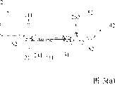
图10是本发明的第九实施例所涉及的半导体摄像装置(光学器件)8的剖面图。本实施例的半导体摄像装置8是由投影面呈矩形形状的透明部件48、半导体摄像元件28和透明粘合剂118构成的。FIG. 10 is a cross-sectional view of a semiconductor imaging device (optical device) 8 according to a ninth embodiment of the present invention. The
透明部件48为在透明基层材料58的一侧的上表面具有导体布线68。并且,位于导体布线68一侧的端部上的突起电极78,配置在与半导体摄像元件28的电极38相对应的位置上。还有,在导体布线68的另一侧端部设置的外部连接用电极88,以所规定的间隔配置在透明基层材料58的外周区域。并且,这些外部连接用电极88,与设置在透明基层材料58中的贯通电极98连接,并通过该贯通电极98与设置在透明基层材料58的另一面上的二次组装用的背面电极228连接。The
还有,透明部件48的投影面的大小,至少比半导体摄像元件28大,且突起电极78和外部连接用电极88的高度形成为:在突起电极78之中的电极或者在外部连接用电极88之中的电极分别具有相同的高度。不过,在这些电极之间,电极的高度可以设定为相同的高度,或者也可以设定为不同的高度。In addition, the size of the projection surface of the
还有,透明基层材料58是硼硅酸玻璃或特勒克斯玻璃等的硬质玻璃、石英、氧化铝玻璃、环氧类树脂、丙烯酸类树脂以及聚酰亚胺类树脂等,可以使用至少对可见光而言是透明的任意材料。还有,导体布线68,一般是由蒸镀、电镀或者印刷等方法形成的,只要是作为电路衬底等的布线材料被经常使用的,就都可以使用并没有特别的限制。例如能够使用铜、镍、金、铝等的单质结构或者它们的叠层结构。还有,突起电极78和外部连接用电极88,一般是通过电镀工序或引线隆起(wire bump)法形成的,作为它们的材料能够使用例如金、铜或者在铜的表面形成了金薄膜的材料。然而,并不仅局限于这些材料以及形成方法。In addition, the
再者,贯通电极98,一般能够利用蒸镀、电镀或者印刷的方法以埋入的方式形成。作为用于该贯通电极98的材料,能够使用金、铜或其他的一般可在蒸镀等中加以使用的金属材料、或者可以在印刷中加以使用的导电性糊状物等的材料。Furthermore, the through
这些导体布线68、突起电极78、外部连接用电极88以及背面电极228的形成,也可以采用下记方法,即通过例如喷镀法形成上述金属膜以后,利用光微影工序形成导体布线68,然后仅在导体布线68的两端部通过电解电镀形成具有规定高度的突起电极78、外部连接用电极88以及突起状的背面电极228。These
再者,半导体摄像元件28为:其主面是由摄像区域(无图示)和周围电路区域(无图示)以及电极区域(无图示)构成的,在摄像区域内的各像素上形成有微型镜头(无图示)。并且,在微型镜头上层以覆盖除去电极区域内的电极38以外的整个主面的形态形成有透明低折射率膜238和平整膜248构成的叠层有机膜。再者,这些膜也可以只形成在摄像区域。并且,在例如铝或铜构成的电极38的表面上,用无电解电镀等方法形成有例如镍或者镍和金的叠层膜。再者,电极38的表面也可以不像上述所示的那样用镍等覆盖,而是仍保持原有的铝的状态。Furthermore, the
透明粘合剂118是由液态或者半硬化状的具有紫外线硬化特性或者热硬化特性中的任一种特性的透明树脂构成的,能够使用由环氧类树脂、丙烯酸类树脂以及聚酰亚胺类树脂中的任意材料构成的粘合剂。再者,也不一定局限于这些材料,只要是具有透明性和粘合特性的材料都可以使用。The
本实施例中的半导体摄像装置8为:在构成透明部件48的透明基层材料58的一侧的上表面形成的突起电极78和电极38相接触并进行电连接,且由于充填在透明基层材料58和半导体摄像元件28之间间隙处的透明粘合剂118而被粘合固定。也就是,突起电极78和电极38之间的电连接,是在半导体摄像元件28的整个主面涂敷了透明粘合剂118以后,对突起电极78和电极38进行位置对准并在加压的状态下实现的,且通过从透明基层材料58的背面一侧(没有形成导体布线68的面的一侧)照射紫外线进行硬化从而保持连接。再者,由此也能够对透明基层材料58和半导体摄像元件28之间进行粘合。并且,在紫外线照射以后,也可以加热促进硬化。还有,透明粘合剂118也可以在对突起电极78和电极38进行位置对准后,在对透明部件48和半导体摄像元件28这两者间加压的同时进行填充,且在此状态下照射紫外线使其硬化。The
再者,关于配置在透明基层材料58的导体布线68上的突起电极78和半导体摄像元件28的电极38的接合,也能够用导电性粘合剂或焊锡进行连接、或者用超音波连接等方法加以实施。Furthermore, with regard to the bonding of the protruding
根据这种结构,在与透明部件48的搭载有半导体摄像元件28的面相反一侧的透明部件48的面上,也可以搭载其他的组装用衬底。因此,不仅能够实现半导体摄像模块机能的高密度化,还能够使进行自由设计的空间得以扩大。再者,能够实现轻·薄·小型的半导体摄像装置8。According to such a configuration, another assembly substrate can be mounted on the surface of the
(第十实施例)(tenth embodiment)
图11是第十实施例所涉及的半导体摄像装置9的剖面图。本实施例的半导体摄像装置9,其特征在于将在第九实施例的半导体摄像装置8中使用的透明部件48的突起形状的背面电极228改为平面形状的背面电极259。其他的构成和材质与第九实施例所涉及的半导体摄像装置8相同。因此,在此省略对它们的详细说明。FIG. 11 is a cross-sectional view of a semiconductor imaging device 9 according to the tenth embodiment. The semiconductor imaging device 9 of the present embodiment is characterized in that the protrusion-shaped
再者,第九实施例的半导体摄像装置8以及第十实施例的半导体摄像装置9,也可以分别适用于在第二到第七实施例中已经加以说明的透明部件的结构。通过应用该结构,能够获得与第一实施例相同的效果。Furthermore, the
(第十一实施例)(eleventh embodiment)
图12是本发明的第十一实施例所涉及的半导体摄像模块(光学模块)18的剖面图。图12中所示的本实施例所涉及的半导体摄像模块18是由将第九实施例中已经说明的半导体摄像装置8,分别组装在第一组装用衬底128和第二组装用衬底178上的结构构成的。FIG. 12 is a cross-sectional view of a semiconductor imaging module (optical module) 18 according to an eleventh embodiment of the present invention. The
第一组装用衬底128为:在第一基层材料138的一面上,具有形状至少比半导体摄像元件28大且深度比半导体摄像元件28的厚度大的凹部148。并且,在该凹部148的周围部,形成有多条第一衬底布线168。还有,在第一衬底布线168的一侧设置的第一衬底端子158,配置在与设置于半导体摄像装置18的透明部件48上的外部连接用电极88相对应的位置上。第一衬底布线168的另一侧的端部以所规定的间隔配置在第一基层材料138的周围部。The
第一基层材料138能够使用例如玻璃环氧树脂、芳香族聚酰胺纤维无纺布、聚酰亚胺树脂、各种陶瓷、及表面上具有绝缘膜的金属板中的任一种材料。For the
第二组装用衬底178为:具有贯通第二基层材料188的贯通开口198,且在该贯通开口198的周围部形成有第二衬底布线218。并且,在第二衬底布线218的一侧设置的第二衬底端子208,配置在与半导体摄像装置8的透明部件48上形成的背面电极228相对应的位置上。还有,第二衬底布线218的另一侧的端部以所规定的间隔被配置在第二基层材料188的周围部。再者,第二基层材料188的贯通开口198的开口尺寸构成为:该贯通开口198的投影面积至少在半导体摄像元件28的摄像区域以上。也就是,通过贯通开口198进入的光,入射到半导体摄像元件28的至少整个摄像区域中。The
第二基层材料188也能够使用例如玻璃环氧树脂、芳香族聚酰胺纤维无纺布、聚酰亚胺树脂、各种陶瓷、及表面上具有绝缘膜的金属板中的任一种材料。For the
本实施例的半导体摄像模块18能够按照下记方法进行制作。也就是,将半导体摄像元件28插入到在构成第一组装用衬底128的第一基层材料1The
38的一面上设置的凹部148中,且直到半导体摄像装置8的外部连接用电极88与形成于第一基层材料138的第一衬底端子158相接触的位置上。在这种状态下,对透明部件48的外部连接用电极88和第一基层材料138的第一衬底端子158进行位置对准。并且,在两者间加热、加压,进行电接合和机械式粘合。再者,两者间的接合也可以使用焊锡接合或热硬化型导电粘合剂等。38 and up to the position where the
其后,将在构成第二组装用衬底178的第二基层材料188上形成的第二衬底端子208和透明部件48的背面电极228之间进行位置对准并使它们相接触。此时,进行位置调整从而使半导体摄像装置8的半导体摄像元件28的摄像区域没有被贯通开口198的外缘部分所遮蔽。在这种状态下,对背面电极228和第二衬底端子208之间进行接合。Thereafter, the
再者,第一组装用衬底128和半导体装置8之间的接合,也可以用焊锡接合或热硬化型导电粘合剂等进行接合。还有,使用相同的方法也可以将半导体摄像装置8和第一组装用衬底128以及第二组装用衬底178同时进行接合。Furthermore, the bonding between the
根据这种结构,能够实现高密度、且轻·薄·小型的半导体摄像模块18。还有,由于该结构具有两块组装用衬底,从而能够将诸如一侧的组装用衬底上所设置的导体布线作为电源线和接地线加以使用,且将另一侧的组装用衬底上所设置的导体布线作为信号线加以区分使用。使用图10所示的半导体摄像装置8组装成这种结构时,可以将第一组装用衬底128的导体布线168和第二组装用衬底178的导体布线218分别制作成不同的布线图案。例如,将第二组装用衬底178上所设置的作为接地线的导体布线218连接到半导体摄像装置8的接地线的背面电极端子228上时,也可以不用形成与之对应的连接到外部连接用电极88上的导体布线168。这样一来,根据第一组装用衬底128以及第二组装用衬底178各自的导体布线168、218的图案设计,能够自由地对接地线和电源线加以区分并进行连接。According to such a configuration, it is possible to realize a high-density
再者,外部连接用电极88和背面电极228,也可以在形成透明部件48的工序中,形成为相互之间预先电分离的形态。这种布线结构也包含在本发明的范围中。In addition, the
(第十二实施例)(twelfth embodiment)
图13是第十二实施例所涉及的半导体摄像模块19的剖面图。本实施例的半导体摄像模块19,其特征为使用第十实施例的变形例所涉及的半导体摄像装置9进行制作。本实施例的半导体摄像模块19,其特征在于该构成使用了具有柔性的第二组装用衬底179,而除这些以外的其他构成与第十一实施例相同。FIG. 13 is a cross-sectional view of a
该第二组装用衬底179是由下记结构构成的,即在第二基层材料189中使用聚酰亚胺类树脂或聚酯类树脂形成为柔性形态。第二组装用衬底179为:具有贯通第二基层材料189的贯通开口199,且该贯通开口199的周围部形成有第二衬底布线219。并且,在第二衬底布线219的一侧所设置的第二衬底端子209,配置在与半导体摄像装置9的透明部件49上形成的背面电极259相对应的位置上。还有,第二衬底布线219的另一侧的端部,以所规定的间隔配置在第二基层材料189的周围部。再者,第二基层材料189的贯通开口199的开口尺寸构成为:该贯通开口199的投影面积至少在半导体摄像元件28的摄像区域以上。The
其他的构成和材质与第十一实施例所涉及的第二组装用衬底178相同。因此,在此省略对它们的详细说明。Other configurations and materials are the same as those of the
根据这种构成,本实施例的半导体摄像模块19成为具有两块组装用衬底的结构,能够将诸如一侧的组装用衬底上所设置的导体布线作为电源线和接地线加以使用,且将另一侧的组装用衬底上所设置的导体布线作为信号线加以区分使用。再者,通过在第二组装用衬底179中使用柔性材质,从而能够使用于收纳在电子器械中的收纳空间的自由度得以提高。还有,也能够实现轻·薄·小型的半导体摄像模块19。According to this configuration, the
再者,关于已经在第十一以及第十二实施例中说明的半导体摄像装置8以及作为变形例的半导体摄像装置9,也分别适用于在第二到第七实施例中已加以说明的透明部件的结构,应用这些构成也可以使用第十一以及第十二实施例中已说明的第一组装用衬底以及第二组装用衬底来制作半导体摄像模块。Moreover, regarding the
(第十三实施例)(thirteenth embodiment)
图14是表示本发明第十三实施例所涉及的半导体摄像装置10的结构的剖面图。本实施例的半导体摄像装置10,其特征为在与第一实施例中已说明的半导体摄像装置1的透明部件41的一面相对的另一面上,还设置有在镜头支架302上安装有镜头301的镜头模块300。该镜头模块300,是在镜头301相对于半导体摄像元件21的摄像区域进行光轴对准的情况下安装的。还有,镜头模块300的构成包括镜筒303、设置在该镜筒303内部的镜头支架302以及固定在镜头支架302上的镜头301。该镜头模块300为固定焦点型,是被用于诸如手机等的镜头模块。FIG. 14 is a cross-sectional view showing the structure of a semiconductor imaging device 10 according to a thirteenth embodiment of the present invention. The semiconductor imaging device 10 of this embodiment is characterized in that, on the other side opposite to the
在本实施例中,作为透明部件41的透明基层材料51,如果使用诸如玻璃衬底的话,就能够通过简单的工序对安装镜头模块300时的光轴进行调整等,并能进行粘合固定。也就是,能够将半导体摄像元件21以其摄像区域和玻璃衬底平行且以高精度组装到作为透明基层材料51的玻璃衬底上。还有,因为玻璃衬底具有非常良好的平整性,所以能够在保持高精度的平行状态下粘贴镜头模块300。同时,也能够简单地进行光轴位置的调准。根据这种结构,即使在安装上镜头模块300的状态下,仍能够实现整体薄型化的半导体摄像装置10。In this embodiment, if a glass substrate is used as the
再者,在第二到第七实施例中已进行说明的半导体摄像装置的另一面上,也可以与本实施例同样安装上镜头模块300。Furthermore, the
(第十四实施例)(fourteenth embodiment)
图15是使用图14中所示的半导体摄像装置10,组装到第一组装用衬底121上从而构成的半导体摄像模块20的剖面图。因为第一组装用衬底121使用的是与已在第八实施例中说明的组装用衬底相同的衬底,所以省略对它的说明。还有,因为能够使用与在第八实施例中已说明的工序相同的工序来制作本实施例的半导体摄像模块20,所以也省略对制作工序的说明。FIG. 15 is a cross-sectional view of a
这种半导体摄像模块20,能够以简单的工序、并在高精度的状态下安装镜头模块300。再者,将半导体摄像元件21向第一组装用衬底121的凹部141中的埋入以及、将外部连接用电极和第一组装用衬底121的第一衬底端子151之间的连接都是以覆晶方式进行的,从而即使在安装了镜头模块300的状态下,与以往的结构相比仍能实现薄型化。因此,在诸如手机等要求薄型化的领域中具有特别显著的效果。Such a
还有,在本实施例中其构成为:在第一组装用衬底121中设置有凹部141,并将半导体摄像元件21插入到该凹部141中,但本发明并不仅局限于此。例如,也可以使用下述所示的第一组装用衬底,即在第一基层材料中设置有至少比半导体摄像元件大的开口部,在该开口部的外周区域与半导体摄像装置的突起电极的位置相对应配置的第一衬底端子和、从第一衬底端子向外部电路部连接的第一衬底布线设置在第一组装用衬底上。也可以将本实施例的半导体摄像装置10组装到具有这种形状的第一组装用衬底上,从而构成半导体摄像模块。In addition, in this embodiment, the
再者,在镜头模块上安装有马达或者传感器等的时候,也可以将镜头模块安装在第三实施例中已说明的使用了设置有贯通电极的透明部件的半导体摄像装置的透明基层材料的另一面上。此时,也可以利用诸如焊接等方法对镜头模块的马达等电气部件的电极端子和背面电极进行连接。并且,如果利用贯通电极将背面电极和所设置的外部连接用电极进行连接的话,也能够通过形成在第一组装用衬底上的电路对马达等进行控制。Furthermore, when a motor or a sensor is mounted on the lens module, the lens module may also be mounted on another transparent base material of the semiconductor imaging device described in the third embodiment using a transparent member provided with a penetrating electrode. on the one hand. At this time, the electrode terminals of the electrical components such as the motor of the lens module and the back electrode may also be connected by a method such as welding. In addition, if the back electrode is connected to the provided external connection electrode by the through-electrode, it is also possible to control the motor or the like through the circuit formed on the first assembly substrate.
还有,上述实施例中,受光区域仅在第一实施例的图2(a)、及图8(a)中加以标注,而所有的实施例和变形例所涉及的透明部件中都存在受光区域。受光区域是被突起电极包围的区域,是将位于透明基层材料的一面的中央部一侧的导体布线的前端相连结而成的区域。In addition, in the above-mentioned embodiments, the light-receiving area is only marked in Fig. 2(a) and Fig. 8(a) of the first embodiment, and there are light-receiving areas in the transparent parts involved in all embodiments and modifications. area. The light-receiving region is a region surrounded by the protruding electrodes, and is a region formed by connecting the ends of the conductor wirings positioned at the center of one surface of the transparent base material.
还有,在上述的实施例中,也可以用发光二极管元件取代半导体摄像元件。也可以用其他的进行受光或者发光的光学元件来取代光学摄像元件。此时,透明部件和第一及第二组装用衬底的结构和功能与上述实施例中所记载的透明部件和第一及第二组装用衬底的结构和功能相同。In addition, in the above-mentioned embodiments, a light emitting diode element may be used instead of a semiconductor imaging element. Instead of the optical imaging element, other optical elements that receive or emit light may also be used. In this case, the structures and functions of the transparent member and the first and second assembly substrates are the same as those of the transparent member and the first and second assembly substrates described in the above embodiments.
(产业上的利用可能性)(Industrial Utilization Possibility)
如以上所说明的那样,因为本发明所涉及的半导体摄像装置,是由对在位于透明部件的导体布线上所设置的突起电极和半导体摄像元件的电极用覆晶方式进行连接的结构构成的,且使用该半导体摄像装置构成的半导体摄像模块构成为将半导体摄像元件插入到第一组装用衬底的凹部的这一结构,所以能够实现轻·薄·小型的半导体摄像模块,对于手机或数码照相机等使用半导体摄像元件的电子器械领域等是有用的。As described above, since the semiconductor imaging device according to the present invention is constituted by flip-chip connection between the protruding electrodes provided on the conductor wirings located on the transparent member and the electrodes of the semiconductor imaging element, Moreover, the semiconductor imaging module constructed using this semiconductor imaging device has a structure in which the semiconductor imaging element is inserted into the concave portion of the first assembly substrate, so a light, thin, and small semiconductor imaging module can be realized. It is useful in the field of electronic equipment and the like using a semiconductor imaging element.
Claims (19)
Translated fromChineseApplications Claiming Priority (3)
| Application Number | Priority Date | Filing Date | Title |
|---|---|---|---|
| JP2006126610 | 2006-04-28 | ||
| JP2006126610AJP2007299929A (en) | 2006-04-28 | 2006-04-28 | Optical device apparatus and optical device module using the same |
| JP2006-126610 | 2006-04-28 |
Publications (2)
| Publication Number | Publication Date |
|---|---|
| CN101064329Atrue CN101064329A (en) | 2007-10-31 |
| CN101064329B CN101064329B (en) | 2010-12-15 |
Family
ID=38647553
Family Applications (1)
| Application Number | Title | Priority Date | Filing Date |
|---|---|---|---|
| CN2007100057404AExpired - Fee RelatedCN101064329B (en) | 2006-04-28 | 2007-02-13 | Optical apparatus and optical module using the same |
Country Status (3)
| Country | Link |
|---|---|
| US (1) | US7582944B2 (en) |
| JP (1) | JP2007299929A (en) |
| CN (1) | CN101064329B (en) |
Cited By (9)
| Publication number | Priority date | Publication date | Assignee | Title |
|---|---|---|---|---|
| CN102084507A (en)* | 2008-07-01 | 2011-06-01 | 皇家飞利浦电子股份有限公司 | Wavelength converted light emitting diode with reduced emission of unconverted light |
| CN102884645A (en)* | 2010-01-29 | 2013-01-16 | 西铁城电子株式会社 | Method for producing light-emitting device and light emitting device |
| CN103000795A (en)* | 2011-09-15 | 2013-03-27 | 隆达电子股份有限公司 | Packaging structure of semiconductor light-emitting element |
| CN104319337A (en)* | 2014-10-29 | 2015-01-28 | 杨晓丽 | Substrate-free LED device and manufacturing method thereof |
| CN105991909A (en)* | 2015-03-16 | 2016-10-05 | 豪威科技股份有限公司 | Optical assemblies including dry adhesive layers and associated methods |
| CN107924924A (en)* | 2015-08-10 | 2018-04-17 | 大日本印刷株式会社 | Image sensor module |
| CN108307591A (en)* | 2017-01-13 | 2018-07-20 | 奥特斯奥地利科技与系统技术有限公司 | Pass through the component load-bearing part manufactured with attachment coating member before being installed on component carrier material |
| CN109390449A (en)* | 2017-08-02 | 2019-02-26 | Lg 伊诺特有限公司 | Light emitting device package |
| US11410896B2 (en) | 2016-02-08 | 2022-08-09 | Sony Corporation | Glass interposer module, imaging device, and electronic apparatus |
Families Citing this family (53)
| Publication number | Priority date | Publication date | Assignee | Title |
|---|---|---|---|---|
| KR100723492B1 (en)* | 2005-07-18 | 2007-06-04 | 삼성전자주식회사 | Display driver integrated circuit devices and films and modules containing them |
| TWI320545B (en)* | 2006-10-05 | 2010-02-11 | Chipmos Technologies Inc | Film type package for fingerprint sensor |
| JP5295783B2 (en) | 2007-02-02 | 2013-09-18 | セミコンダクター・コンポーネンツ・インダストリーズ・リミテッド・ライアビリティ・カンパニー | Semiconductor device |
| US7855425B2 (en)* | 2007-03-09 | 2010-12-21 | Sanyo Electric Co., Ltd. | Semiconductor device and method of manufacturing the same |
| TW200904159A (en)* | 2007-07-06 | 2009-01-16 | Kye Systems Corp | Thin type image capturing module |
| US7880309B2 (en)* | 2007-07-30 | 2011-02-01 | Qimonda Ag | Arrangement of stacked integrated circuit dice having a direct electrical connection |
| JP2009283902A (en)* | 2008-04-25 | 2009-12-03 | Panasonic Corp | Optical device and electronic apparatus including the same |
| TWI384602B (en)* | 2008-06-13 | 2013-02-01 | Unimicron Technology Corp | Package substrate embedded with photosensitive semiconductor wafer and preparation method thereof |
| US7781854B2 (en)* | 2008-07-31 | 2010-08-24 | Unimicron Technology Corp. | Image sensor chip package structure and method thereof |
| JP5376865B2 (en) | 2008-08-19 | 2013-12-25 | キヤノン株式会社 | Solid-state imaging device and electronic imaging device |
| JP4710936B2 (en)* | 2008-08-29 | 2011-06-29 | 富士ゼロックス株式会社 | Exposure equipment |
| JP2010171307A (en)* | 2009-01-26 | 2010-08-05 | Panasonic Corp | Imaging device |
| JP5515357B2 (en)* | 2009-03-26 | 2014-06-11 | 株式会社ニコン | Imaging device and imaging module using the same |
| US8212263B2 (en)* | 2009-04-03 | 2012-07-03 | Koninklijke Philips Electronics N.V. | Backlight including semiconductior light emitting devices |
| TWM377018U (en)* | 2009-09-09 | 2010-03-21 | Azurewave Technologies Inc | Flip chip type image capturing module |
| JP2011066093A (en)* | 2009-09-15 | 2011-03-31 | Olympus Corp | Imaging unit |
| WO2011055655A1 (en)* | 2009-11-05 | 2011-05-12 | コニカミノルタオプト株式会社 | Image pickup device, optical unit, wafer lens laminated body, and method for manufacturing wafer lens laminated body |
| CN102379039B (en)* | 2009-11-26 | 2015-04-01 | 京瓷株式会社 | Wiring board, imaging device, and imaging device module |
| JP5771898B2 (en)* | 2010-03-17 | 2015-09-02 | 株式会社ニコン | Image sensor and camera |
| TW201138123A (en)* | 2010-04-28 | 2011-11-01 | Hon Hai Prec Ind Co Ltd | Image sensor package structure and camera module using same |
| EP2587793B1 (en)* | 2010-06-28 | 2020-01-08 | Kyocera Corporation | Image pickup device and image-pickup device module |
| WO2012002580A1 (en)* | 2010-07-01 | 2012-01-05 | シチズンホールディングス株式会社 | Led light source device and method for manufacturing same |
| JP2012028550A (en)* | 2010-07-23 | 2012-02-09 | Panasonic Corp | Sensor package, imaging device, and portable electronic appliance |
| JP2012029028A (en)* | 2010-07-23 | 2012-02-09 | Panasonic Corp | Sensor package, imaging apparatus and portable electronic apparatus |
| DE102010032512A1 (en)* | 2010-07-28 | 2012-02-02 | Osram Opto Semiconductors Gmbh | A light-emitting semiconductor component and method for producing a light-emitting semiconductor component |
| JP5221615B2 (en)* | 2010-09-21 | 2013-06-26 | 株式会社東芝 | Imaging device and manufacturing method thereof |
| JP2012134397A (en)* | 2010-12-22 | 2012-07-12 | Seiko Instruments Inc | Optical device module |
| JP5296130B2 (en)* | 2011-03-22 | 2013-09-25 | シャープ株式会社 | Optical module and optical module manufacturing method |
| JP5736253B2 (en)* | 2011-06-30 | 2015-06-17 | セイコーインスツル株式会社 | Optical sensor device |
| US8952402B2 (en) | 2011-08-26 | 2015-02-10 | Micron Technology, Inc. | Solid-state radiation transducer devices having flip-chip mounted solid-state radiation transducers and associated systems and methods |
| JP2013105784A (en)* | 2011-11-10 | 2013-05-30 | Seiko Instruments Inc | Optical sensor device and method for manufacturing the same |
| JP6056186B2 (en)* | 2012-05-08 | 2017-01-11 | 株式会社ニコン | Image sensor |
| US10252674B2 (en)* | 2012-12-17 | 2019-04-09 | Lg Innotek Co., Ltd. | Blind spot detection module |
| US9276030B2 (en)* | 2013-03-15 | 2016-03-01 | Sensors Unlimited, Inc. | Read out integrated circuit input/output routing on permanent carrier |
| US9000344B2 (en)* | 2013-03-15 | 2015-04-07 | Sensors Unlimited, Inc. | Focal plane array periphery through-vias for read out integrated circuit |
| WO2015014393A1 (en)* | 2013-07-30 | 2015-02-05 | Osram Opto Semiconductors Gmbh | Optoelectronic device |
| JP5631457B2 (en)* | 2013-08-05 | 2014-11-26 | キヤノン株式会社 | Solid-state imaging device and electronic imaging device |
| WO2015122299A1 (en)* | 2014-02-13 | 2015-08-20 | ソニー株式会社 | Solid-state imaging device, electronic apparatus, and solid-state imaging device manufacturing method |
| JP5811220B2 (en)* | 2014-03-28 | 2015-11-11 | 株式会社ニコン | Imaging module |
| JP2015198172A (en)* | 2014-04-01 | 2015-11-09 | 株式会社フジクラ | Optical module and method for manufacturing the same |
| JP2015220291A (en)* | 2014-05-15 | 2015-12-07 | 株式会社ソシオネクスト | Semiconductor device and method of manufacturing the same |
| JP6314070B2 (en)* | 2014-10-07 | 2018-04-18 | 新光電気工業株式会社 | Fingerprint recognition semiconductor device, method for manufacturing fingerprint recognition semiconductor device, and semiconductor device |
| JP5908627B2 (en)* | 2015-03-13 | 2016-04-26 | エスアイアイ・セミコンダクタ株式会社 | Optical sensor device |
| JP6416384B2 (en)* | 2015-04-03 | 2018-10-31 | シャープ株式会社 | The camera module |
| TWI656632B (en)* | 2017-05-12 | 2019-04-11 | 海華科技股份有限公司 | Portable electronic device and image capturing module and bearing component thereof |
| WO2019007412A1 (en)* | 2017-07-06 | 2019-01-10 | 苏州晶方半导体科技股份有限公司 | Encapsulation structure of image sensing chip, and encapsulation method therefor |
| KR102730308B1 (en)* | 2019-01-30 | 2024-11-15 | 에스케이하이닉스 주식회사 | Semiconductor memory device and method of manufacturing the same |
| US20220246665A1 (en)* | 2019-07-23 | 2022-08-04 | Sony Semiconductor Solutions Corporation | Semiconductor package |
| JP7373336B2 (en)* | 2019-09-20 | 2023-11-02 | ニデックプレシジョン株式会社 | Circuit board and imaging device |
| WO2022085326A1 (en)* | 2020-10-22 | 2022-04-28 | ソニーセミコンダクタソリューションズ株式会社 | Imaging device, electronic apparatus, and method for manufacturing imaging device |
| KR20220070766A (en) | 2020-11-23 | 2022-05-31 | 삼성전자주식회사 | Image sensor package including glass substrate |
| JP2024123285A (en)* | 2021-07-21 | 2024-09-11 | ソニーセミコンダクタソリューションズ株式会社 | Semiconductor Package |
| WO2024111248A1 (en)* | 2022-11-24 | 2024-05-30 | ソニーセミコンダクタソリューションズ株式会社 | Semiconductor package, optical device, and method for producing semiconductor package |
Family Cites Families (9)
| Publication number | Priority date | Publication date | Assignee | Title |
|---|---|---|---|---|
| JPS63242072A (en) | 1987-03-30 | 1988-10-07 | Toshiba Corp | solid state imaging device |
| US5359190A (en)* | 1992-12-31 | 1994-10-25 | Apple Computer, Inc. | Method and apparatus for coupling an optical lens to an imaging electronics array |
| JPH0917986A (en) | 1995-06-30 | 1997-01-17 | Sony Corp | Solid state image pickup device and manufacturing method thereof |
| JP2002026301A (en)* | 2000-07-07 | 2002-01-25 | Toshiba Corp | Photoelectric conversion device and method of manufacturing the same |
| JP4239466B2 (en)* | 2002-04-12 | 2009-03-18 | ソニー株式会社 | Semiconductor device and manufacturing method thereof |
| US7274094B2 (en)* | 2002-08-28 | 2007-09-25 | Micron Technology, Inc. | Leadless packaging for image sensor devices |
| JP4126389B2 (en)* | 2002-09-20 | 2008-07-30 | カシオ計算機株式会社 | Manufacturing method of semiconductor package |
| JP2005347398A (en)* | 2004-06-01 | 2005-12-15 | Fuji Photo Film Co Ltd | Packaging substrate for solid-state image pickup device, camera module, and portable telephone |
| US7342268B2 (en)* | 2004-12-23 | 2008-03-11 | International Business Machines Corporation | CMOS imager with Cu wiring and method of eliminating high reflectivity interfaces therefrom |
- 2006
- 2006-04-28JPJP2006126610Apatent/JP2007299929A/enactivePending
- 2007
- 2007-01-26USUS11/698,100patent/US7582944B2/ennot_activeExpired - Fee Related
- 2007-02-13CNCN2007100057404Apatent/CN101064329B/ennot_activeExpired - Fee Related
Cited By (14)
| Publication number | Priority date | Publication date | Assignee | Title |
|---|---|---|---|---|
| CN102084507B (en)* | 2008-07-01 | 2016-01-20 | 皇家飞利浦电子股份有限公司 | What have reduction does not change photoemissive wavelength convert light-emitting diode |
| CN102084507A (en)* | 2008-07-01 | 2011-06-01 | 皇家飞利浦电子股份有限公司 | Wavelength converted light emitting diode with reduced emission of unconverted light |
| CN102884645A (en)* | 2010-01-29 | 2013-01-16 | 西铁城电子株式会社 | Method for producing light-emitting device and light emitting device |
| CN102884645B (en)* | 2010-01-29 | 2015-05-27 | 西铁城电子株式会社 | Method for producing light-emitting device and light emitting device |
| CN103000795A (en)* | 2011-09-15 | 2013-03-27 | 隆达电子股份有限公司 | Packaging structure of semiconductor light-emitting element |
| CN103000795B (en)* | 2011-09-15 | 2015-10-28 | 隆达电子股份有限公司 | Packaging structure of semiconductor light-emitting element |
| CN104319337A (en)* | 2014-10-29 | 2015-01-28 | 杨晓丽 | Substrate-free LED device and manufacturing method thereof |
| CN105991909A (en)* | 2015-03-16 | 2016-10-05 | 豪威科技股份有限公司 | Optical assemblies including dry adhesive layers and associated methods |
| CN107924924A (en)* | 2015-08-10 | 2018-04-17 | 大日本印刷株式会社 | Image sensor module |
| CN107924924B (en)* | 2015-08-10 | 2022-12-06 | 大日本印刷株式会社 | Image sensor module |
| US11410896B2 (en) | 2016-02-08 | 2022-08-09 | Sony Corporation | Glass interposer module, imaging device, and electronic apparatus |
| CN108307591A (en)* | 2017-01-13 | 2018-07-20 | 奥特斯奥地利科技与系统技术有限公司 | Pass through the component load-bearing part manufactured with attachment coating member before being installed on component carrier material |
| CN109390449A (en)* | 2017-08-02 | 2019-02-26 | Lg 伊诺特有限公司 | Light emitting device package |
| CN109390449B (en)* | 2017-08-02 | 2023-03-28 | 苏州立琻半导体有限公司 | Light emitting device package |
Also Published As
| Publication number | Publication date |
|---|---|
| CN101064329B (en) | 2010-12-15 |
| US7582944B2 (en) | 2009-09-01 |
| JP2007299929A (en) | 2007-11-15 |
| US20070252227A1 (en) | 2007-11-01 |
Similar Documents
| Publication | Publication Date | Title |
|---|---|---|
| CN101064329A (en) | Optical apparatus and optical module using the same | |
| CN1832163A (en) | Camera module and manufacturing method thereof | |
| CN100342281C (en) | Imaging device packaging, camera module and the producing process of the camera module | |
| CN1192338C (en) | Electro-optical device, manufacturing method thereof, and electronic device | |
| CN1157052C (en) | Camera device, manufacturing method thereof, and electrical equipment | |
| CN1176496C (en) | Semiconductor device and mfg. method thereof | |
| CN1713214A (en) | Image pickup device and production method thereof | |
| CN1722453A (en) | Imaging and Electronics | |
| CN1423477A (en) | Solid-state imaging device and manufacturing method thereof | |
| CN1225111C (en) | small camera module | |
| CN1652341A (en) | optical instrument | |
| CN1783951A (en) | Small image pickup module | |
| CN101055866A (en) | Module for optical device and manufacturing method thereof | |
| CN1684284A (en) | Optical semiconductor device and electronic device using same | |
| CN1697190A (en) | Optical device and manufacturing method thereof | |
| CN1501696A (en) | Camera device and portable terminal device | |
| CN1577736A (en) | Module with a built-in semiconductor and method for producing the same | |
| CN1429014A (en) | Solid-state imaging device and its mfg. method | |
| CN1677660A (en) | Semiconductor device, manufacturing method thereof, semiconductor module device, and wiring substrate | |
| CN1264037C (en) | Optical modular, its mfg. method and electronic instrument | |
| CN101048039A (en) | Optical/electrical circuit interconnect board and evaluation method therefor | |
| CN1909237A (en) | Semiconductor image sensor and method for fabricating the same | |
| CN1649162A (en) | Light Sensor Module | |
| JP2009222740A (en) | Lens module and camera module | |
| CN1728364A (en) | Optical semiconductor devices, optical connectors, and electronic equipment |
Legal Events
| Date | Code | Title | Description |
|---|---|---|---|
| C06 | Publication | ||
| PB01 | Publication | ||
| C10 | Entry into substantive examination | ||
| SE01 | Entry into force of request for substantive examination | ||
| C14 | Grant of patent or utility model | ||
| GR01 | Patent grant | ||
| CF01 | Termination of patent right due to non-payment of annual fee | Granted publication date:20101215 Termination date:20190213 | |
| CF01 | Termination of patent right due to non-payment of annual fee |