CN101059740A - Touch panel and manufacturing method thereof - Google Patents
Touch panel and manufacturing method thereofDownload PDFInfo
- Publication number
- CN101059740A CN101059740ACNA2007100964825ACN200710096482ACN101059740ACN 101059740 ACN101059740 ACN 101059740ACN A2007100964825 ACNA2007100964825 ACN A2007100964825ACN 200710096482 ACN200710096482 ACN 200710096482ACN 101059740 ACN101059740 ACN 101059740A
- Authority
- CN
- China
- Prior art keywords
- substrate
- touch panel
- adhesive layer
- wiring
- conductive layer
- Prior art date
- Legal status (The legal status is an assumption and is not a legal conclusion. Google has not performed a legal analysis and makes no representation as to the accuracy of the status listed.)
- Granted
Links
Images

Classifications
- G—PHYSICS
- G06—COMPUTING OR CALCULATING; COUNTING
- G06F—ELECTRIC DIGITAL DATA PROCESSING
- G06F3/00—Input arrangements for transferring data to be processed into a form capable of being handled by the computer; Output arrangements for transferring data from processing unit to output unit, e.g. interface arrangements
- G06F3/01—Input arrangements or combined input and output arrangements for interaction between user and computer
- G06F3/03—Arrangements for converting the position or the displacement of a member into a coded form
- G06F3/041—Digitisers, e.g. for touch screens or touch pads, characterised by the transducing means
- G06F3/0412—Digitisers structurally integrated in a display
- G—PHYSICS
- G06—COMPUTING OR CALCULATING; COUNTING
- G06F—ELECTRIC DIGITAL DATA PROCESSING
- G06F3/00—Input arrangements for transferring data to be processed into a form capable of being handled by the computer; Output arrangements for transferring data from processing unit to output unit, e.g. interface arrangements
- G06F3/01—Input arrangements or combined input and output arrangements for interaction between user and computer
- G06F3/03—Arrangements for converting the position or the displacement of a member into a coded form
- G06F3/041—Digitisers, e.g. for touch screens or touch pads, characterised by the transducing means
- G06F3/0416—Control or interface arrangements specially adapted for digitisers
- G06F3/04164—Connections between sensors and controllers, e.g. routing lines between electrodes and connection pads
- G—PHYSICS
- G06—COMPUTING OR CALCULATING; COUNTING
- G06F—ELECTRIC DIGITAL DATA PROCESSING
- G06F3/00—Input arrangements for transferring data to be processed into a form capable of being handled by the computer; Output arrangements for transferring data from processing unit to output unit, e.g. interface arrangements
- G06F3/01—Input arrangements or combined input and output arrangements for interaction between user and computer
- G06F3/03—Arrangements for converting the position or the displacement of a member into a coded form
- G06F3/041—Digitisers, e.g. for touch screens or touch pads, characterised by the transducing means
- G06F3/045—Digitisers, e.g. for touch screens or touch pads, characterised by the transducing means using resistive elements, e.g. a single continuous surface or two parallel surfaces put in contact
Landscapes
- Engineering & Computer Science (AREA)
- General Engineering & Computer Science (AREA)
- Theoretical Computer Science (AREA)
- Human Computer Interaction (AREA)
- Physics & Mathematics (AREA)
- General Physics & Mathematics (AREA)
- Computer Networks & Wireless Communication (AREA)
- Position Input By Displaying (AREA)
- Push-Button Switches (AREA)
Abstract
Translated fromChinese
Description
Translated fromChinese技术领域technical field
本发明主要涉及用于各种电子设备的操作的触摸面板及其制造方法。The present invention mainly relates to a touch panel used for operation of various electronic devices and a manufacturing method thereof.
背景技术Background technique
近年来,伴随着便携式电话、汽车导航装置等各种电子设备的高性能化、多样化的进展,在液晶等显示元件的前表面上安装透光性触摸面板,一边通过该触摸面板确认背表面的显示元件的显示,一边用手指、触摸笔等按压操作触摸面板,由此进行设备的各功能的切换的设备逐渐增加。作为这样的触摸面板,要求可视性优异,操作可靠。In recent years, with the advancement of performance and diversification of various electronic devices such as mobile phones and car navigation devices, a light-transmitting touch panel is mounted on the front surface of a display element such as a liquid crystal, and the rear surface is confirmed through the touch panel. Devices that switch functions of the device while pressing and operating the touch panel with a finger, a stylus, or the like while displaying the display element of the device are increasing. Such a touch panel is required to be excellent in visibility and reliable in operation.
对于这样的以往的触摸面板及其制造方法,使用图3以及图4进行说明。Such a conventional touch panel and its manufacturing method will be described using FIGS. 3 and 4 .
另外,为了使结构容易理解,在附图上将厚度方向的尺寸放大进行表示。In addition, in order to make the structure easy to understand, the dimensions in the thickness direction are enlarged and shown in the drawings.
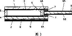
图3是以往的触摸面板的剖面图,图4是其分解立体图。在该图中,在薄膜状透光性的上基板1的下表面上形成有由氧化铟锡等构成的透光性上导电层3,同样在薄膜状透光性的下基板2的上表面上形成有同样的下导电层4。FIG. 3 is a sectional view of a conventional touch panel, and FIG. 4 is an exploded perspective view thereof. In this figure, a light-transmitting upper
然后,在下导电层4的上表面上通过绝缘树脂以规定间隔形成多个点状隔离物(未图示),同时在上导电层3上形成由银等构成的一对上电极3A,在下导电层4上形成与上电极3A垂直方向上的一对下电极4A。Then, on the upper surface of the lower
另外,通过涂布形成于大致画框状的隔离物5的上下表面上的粘接层(未图示),上基板1与下基板2的外周被贴合在一起,上导电层3与下导电层4隔着规定的间隙相对,其中所述隔离物5形成在上基板1下表面或下基板2上表面的外周上。In addition, the outer peripheries of the
进而,在薄膜状配线基板6的上下表面上,形成有由铜、银等构成的多个配线图形6A、6B,同时在配线基板6的上下表面上除了两端部以外,形成覆盖配线图形6A、6B的绝缘层(未图示)。Furthermore, on the upper and lower surfaces of the film-
另外,该配线基板6的左端(图3中的左端,下同),被夹持在上基板1与下基板2右端(图3中的右端,下同)之间,同时通过将导电颗粒分散在合成树脂内而成的各向异性导电粘接剂7,上基板1下表面的上电极3A与下基板2上表面的下电极4A的端部,被分别粘接连接在配线图形6A、6B的左端。In addition, the left end of the wiring substrate 6 (the left end in FIG. 3, the same below) is clamped between the
进而,用起模片9覆盖形成在下基板2下表面整个面上的粘接层8的下表面,从而构成触摸面板。Furthermore, the lower surface of the
然后,对于这样构成的触摸面板,将起模片9剥离,然后通过下基板2下表面上的粘接层8而将其粘贴在液晶显示元件等的前表面上,从而将其安装在电子设备上。与此同时,使配线基板6向下方弯折,并通过连接用连接器或者锡焊等将配线图形6A、6B右端连接在设备的电子电路(未图示)上。Then, for the touch panel constructed in this way, the
在上面的结构中,在一边确认触摸面板背表面的液晶显示元件的显示,一边用手指或触摸笔等按压操作上基板1上表面时,上基板1挠曲,被按压场所的上导电层3与下导电层4接触。In the above structure, when the upper surface of the
然后,从电子电路经由配线基板6的多个配线图形6A、6B,向上电极3A和下电极4A、上导电层3以及与其垂直方向上的下导电层4顺序施加电压,通过它们的电压比,电子电路检测出被按压的场所,进行设备的各种功能的切换。Then, a voltage is sequentially applied from the electronic circuit to the
另外,在制造这样的触摸面板时,在通过隔离物5将大致相同大小的上基板1与下基板2贴合在一起之后,在延伸出有上电极3A以及下电极4A的端部的上基板1和下基板2的右端之间,夹持配线基板6的左端,并以使其与多个上电极3A和下电极4A重合的方式,对多个配线图形6A、6B进行对位并配置。In addition, when manufacturing such a touch panel, after the
然后,通过工卡模具等对夹持有配线基板6左端的上基板1上表面和下基板2下表面进行加热加压,通过各向异性导电粘接剂7将上电极3A与下电极4A的端部、配线图形6A与6B的左端分别粘接连接,从而将配线基板6连接在上基板1和下基板2上。Then, the upper surface of the
之后,从端部开始按顺序以不使空气进入的方式进行辊压等,将由起模片9覆盖了下表面的粘接层8粘贴在下基板2下表面上,由此连接有配线基板6的触摸面板完成。Thereafter, rolling or the like is performed sequentially from the end so that air does not enter, and the
另外,在制造工序上也可以与上述的作业顺序相反,在形成有下导电层4的下基板2下表面上,预先粘贴粘接层8和起模片9,并对其进行辊压等,然后通过隔离物5粘贴在上基板1上,最后从上基板1上表面和起模片9下表面对连结部加热加压,从而将配线基板6连接在上基板1和下基板2上。In addition, in the manufacturing process, it is also possible to reverse the above-mentioned operation sequence. On the lower surface of the
但是,在按照该顺序制造触摸面板时,在对与配线基板6连接的连结部进行加热加压时,粘接层8也被加热加压,所以会产生该场所的粘接层8变形而向外面鼓出或者粘接层8的粘接力恶化的情况。However, when the touch panel is manufactured in this order, the
因此,通常如上所述,在对配线基板6加热加压从而将其连接之后,在下基板2下表面上粘贴粘接层8和起模片9。但是,此时,不管怎样,在剥离起模片9从而粘贴在液晶显示元件等之上时,在下基板2下表面与粘接层8之间都容易产生有损可视性的气泡等。Therefore, usually, as described above, the
因此,为了防止这样的气泡等,虽然需要时间,但必须如上述那样,在将粘接层8粘贴在下基板2上时,从端部开始按顺序以不使空气进入的方式进行辊压等,花费时间进行粘贴。Therefore, in order to prevent such air bubbles, etc., it takes time, but as described above, when the
另外,作为相关的在先技术文献信息,公开有例如特开2003-58319号公报。In addition, as related prior art document information, for example, JP-A-2003-58319 is disclosed.
但是,在上述以往的触摸面板中,为了得到没有气泡等、可视性良好的产品,在将粘接层8粘贴在下基板2下表面上时,必须从端部开始按顺序以不使空气进入的方式进行辊压等,花费时间进行粘贴,所以具有制造需要时间,价格比较高的问题。However, in the above-mentioned conventional touch panel, in order to obtain a product with no air bubbles and good visibility, when the
发明内容Contents of the invention
本发明的目的在于解决这样的以往的问题,提供一种可视性优异、制造容易且低价的触摸面板及其制造方法。An object of the present invention is to solve such conventional problems, and to provide a touch panel that is excellent in visibility, easy to manufacture, and inexpensive, and a method of manufacturing the same.
因此本发明在形成在下基板的下表面上的粘接层的、与配线基板连接的连接部的下方设置切口部从而构成触摸面板。在下基板下表面上,预先形成在与配线基板连接的连接部的下方设置有切口部的粘接层,并通过辊压等,在较短时间内将气泡等大致完全除去。然后将其贴合在上基板上,最后,对连接部进行加热加压,从而进行配线基板的连接。通过这样,能够得到可视性优异、制造容易且低价的触摸面板及其制造方法。Therefore, in the present invention, a cutout is provided below the connection portion of the adhesive layer formed on the lower surface of the lower substrate to connect to the wiring board, thereby constituting a touch panel. On the lower surface of the lower substrate, an adhesive layer having a notch under the connection to the wiring board is formed in advance, and the air bubbles and the like are almost completely removed in a relatively short period of time by rolling or the like. Then, this is bonded to the upper substrate, and finally, the connecting portion is heated and pressed to connect the wiring substrate. In this way, a touch panel with excellent visibility, easy to manufacture, and inexpensive, and a method for manufacturing the same can be obtained.
附图说明Description of drawings
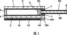
图1是本发明的一个实施方式的触摸面板的剖面图。FIG. 1 is a cross-sectional view of a touch panel according to one embodiment of the present invention.
图2是其分解立体图。Fig. 2 is an exploded perspective view thereof.
图3是以往的触摸面板的剖面图。FIG. 3 is a cross-sectional view of a conventional touch panel.
图4是其分解立体图。Fig. 4 is an exploded perspective view thereof.
具体实施方式Detailed ways
下面,使用图1以及图2对本发明的实施方式进行说明。Next, an embodiment of the present invention will be described using FIG. 1 and FIG. 2 .
另外,为了使结构容易理解,在附图上将厚度方向的尺寸放大进行表示。In addition, in order to make the structure easy to understand, the dimensions in the thickness direction are enlarged and shown in the drawings.
另外,对与背景技术中所说明的结构相同的部分,标以相同符号,并将详细的说明省略。In addition, the same code|symbol is attached|subjected to the same part as the structure demonstrated in background art, and detailed description is abbreviate|omitted.
(实施方式)(implementation mode)
图1是本发明的一个实施方式的触摸面板的剖面图,图2是其分解立体图。在该图中,在由聚对苯二甲酸乙二醇酯、聚碳酸酯等构成的薄膜状透光性的上基板1的下表面上,通过溅射法等形成有由氧化铟锡、氧化锡等构成的透光性上导电层3。同样,在由玻璃、丙烯酸酯或聚碳酸酯等构成的透光性的下基板2的上表面上,通过溅射法等形成有同样的下导电层4。FIG. 1 is a sectional view of a touch panel according to an embodiment of the present invention, and FIG. 2 is an exploded perspective view thereof. In this figure, on the lower surface of a film-shaped light-transmitting
然后,在下导电层4的上表面上,通过环氧树脂、聚硅氧烷等绝缘树脂以规定间隔形成多个点状隔离物(未图示)。在上导电层3上形成由银、碳等构成的上电极3A,在下导电层4上形成与上电极3A垂直方向上的下电极4A。Then, on the upper surface of lower
在上基板1下表面或下基板2上表面的外周上,形成有画框状的由聚酯、环氧树脂等构成的隔离物5。通过形成在隔离物5的上下表面或单面上的丙烯酸酯、橡胶等粘接剂(未图示),上基板1与下基板2的外周被粘贴在一起,上导电层3与下导电层4隔着规定的间隙相对。On the outer periphery of the lower surface of the
进而,在由聚对苯二甲酸乙二醇酯、聚酰亚胺等构成的薄膜状的配线基板6的上下表面上,形成由银、碳、铜等构成的多个配线图形6A、6B,同时在配线基板6的上下表面上除了两端部以外,形成覆盖配线图形6A、6B的绝缘层(未图示)。Furthermore, on the upper and lower surfaces of a film-shaped
然后,该配线基板6的配线图形6A、6B的左端(图1中的左端,下同),通过将在镍、树脂等上实施了镀金而成的多个导电颗粒分散在环氧树脂、丙烯酸酯、聚酯等合成树脂内而成的各向异性导电粘接剂7,被粘接连接在从上基板1下表面和下基板2上表面延伸出的上电极3A和下电极4A端部上。这样,多个配线图形6A、6B经由上电极3A和下电极4A而电气性地连接在上导电层3以及与其垂直方向上的下导电层4上。Then, on the left end of the
进而,用纸、聚对苯二甲酸乙二醇酯等起模片19覆盖形成在下基板2下表面上的丙烯酸酯、聚硅氧烷、氨基甲酸乙酯等粘接层18的下表面。与此同时,在粘接层18和起模片19上的、与配线基板6连接的连接部下方,形成宽度比配线基板6稍大的切口部18A、19A,从而构成触摸面板。Furthermore, the lower surface of the
另外,在制造这样结构的触摸面板时,首先,在形成了下导电层4的下基板2下表面上,粘贴粘接层18和起模片19,然后在该状态下进行辊压等,由此去除在粘贴在液晶显示元件等上时有损可视性的气泡等。In addition, when manufacturing the touch panel with such a structure, first, on the lower surface of the
另外,经由粘接层18而将该下基板2与起模片19贴合在一起的状态,是所有片状的构成部件都层叠在一起的状态。因此,能够通过例如使其通过圆柱状的两个辊子之间等、比较简单的结构,并且在较短时间内,通过辊压而将气泡等大致完全除去。In addition, the state where the
然后,使上基板1与该下基板2重合,通过隔离物5将它们贴合在一起,然后在上基板1与下基板2右端(图1中的右端,下同)之间,以使其与多个上电极3A和下电极4A重合的方式,对多个配线图形6A、6B进行对位,从而夹持配线基板6的左端。Then, the
最后,通过工卡模具等对上基板1上表面和下基板2下表面进行加热加压,通过各向异性导电粘接剂7将上电极3A与下电极4A的端部、配线图形6A与6B的左端分别粘接连接,从而完成连接有配线基板6的触摸面板。Finally, heat and press the upper surface of the
另外,此时在粘接层18和起模片19上的、与配线基板6连接的连接部下方,形成宽度比配线基板6稍大的切口部18A、19A。因此,通过使用比该切口部18A、19A稍小的形状的工卡模具,能够不接触粘接层8和起模片9地直接对下基板2下表面和上基板1上表面进行加热加压。In addition, at this time,
即,在连接该配线基板6时,仅下基板2下表面受到加热加压,在粘接层18上没有施加热量、压力,所以不会产生该场所的粘接层18变形而向外侧鼓出、或者粘接层18的粘接力恶化的情况。That is, when the
进而,由于切口部18A、19A形成为比配线基板6稍大的宽度,所以即使在加热加压时在其与工卡模具之间产生少量的错位,也能够不在粘接层18上施加热量、压力地进行配线基板6的粘接连接。Furthermore, since the
然后,对于这样构成的触摸面板,将起模片19剥离,然后通过下基板2下表面上的粘接层18而将其配置在液晶显示元件等的前表面上,从而将其安装在电子设备上。与此同时,使配线基板6向下方弯折,并通过连接用连接器或者锡焊等将配线图形6A、6B的右端(图1中的右端,下同)连接在设备的电子电路(未图示)上。Then, for the touch panel constructed in this way, the
在上面的结构中,在一边确认触摸面板背表面的液晶显示元件的显示,一边用手指或触摸笔等按压操作上基板1上表面时,上基板1挠曲,被按压场所的上导电层3与下导电层4接触。In the above structure, when the upper surface of the
然后,从电子电路经由配线基板6的多个配线图形6A、6B,向上电极3A和下电极4A、上导电层3以及与其垂直方向上的下导电层4顺序施加电压,通过它们的电压比,电子电路检测出被按压的场所,进行设备的各种功能的切换。Then, a voltage is sequentially applied from the electronic circuit to the
这样,根据本实施方式,在形成在下基板2的下表面上的粘接层18的、与配线基板6连接的连接部下方设置切口部18A。这样,在下基板2下表面上预先形成在与配线基板6连接的连接部下方设置了切口部18A粘接层18。然后,在较短时间内通过辊压等,将其与粘接层18之间的气泡等大致完全除去,然后将其粘贴在上基板1上。最后,对与配线基板6连接的连接部进行加热加压,从而进行配线基板6的连接。因此,能够得到可视性优异、制造容易且低价的触摸面板。Thus, according to the present embodiment, the
另外,在上面的说明中,对在上基板1下表面和下基板2上表面上设置上电极3A和下电极4A、并在其上连接配线基板6上下表面的配线图形6A和6B的左端的结构进行了说明。但是,对于将上下电极双方设置在上基板1或下基板2的任意一个上、并在其上连接配线基板6上表面或下表面的配线图形的结构,也能够实施本发明。In addition, in the above description, the
另外,通常粘接层18粘贴在起模片19上,在该状态下加工切口部18A,所以在上面的说明中,说明了在起模片19上也设置了切口部19A的结构。但是,在通过印刷等在下基板2上表面上形成粘接层18时,也可以是仅在粘接层18上设置切口部18A的结构。In addition, since the
根据本发明,能够得到可视性优异、制造容易且低价的触摸面板,作为操作各种电子设备用的触摸面板非常有用。According to the present invention, it is possible to obtain an inexpensive touch panel with excellent visibility, which is easy to manufacture, and is very useful as a touch panel for operating various electronic devices.
Claims (2)
Translated fromChineseApplications Claiming Priority (2)
| Application Number | Priority Date | Filing Date | Title |
|---|---|---|---|
| JP115188/2006 | 2006-04-19 | ||
| JP2006115188AJP4893082B2 (en) | 2006-04-19 | 2006-04-19 | Touch panel |
Publications (2)
| Publication Number | Publication Date |
|---|---|
| CN101059740Atrue CN101059740A (en) | 2007-10-24 |
| CN101059740B CN101059740B (en) | 2012-07-04 |
Family
ID=38619972
Family Applications (1)
| Application Number | Title | Priority Date | Filing Date |
|---|---|---|---|
| CN2007100964825AExpired - Fee RelatedCN101059740B (en) | 2006-04-19 | 2007-04-19 | Touch panel and manufacturing method thereof |
Country Status (3)
| Country | Link |
|---|---|
| US (1) | US7777733B2 (en) |
| JP (1) | JP4893082B2 (en) |
| CN (1) | CN101059740B (en) |
Cited By (2)
| Publication number | Priority date | Publication date | Assignee | Title |
|---|---|---|---|---|
| CN101673165B (en)* | 2008-09-11 | 2011-09-07 | 比亚迪股份有限公司 | Resistance type glass-glass touch screen and manufacturing method thereof |
| CN102736779A (en)* | 2011-03-29 | 2012-10-17 | 阿尔卑斯电气株式会社 | Input device and method for manufacturing the same |
Families Citing this family (5)
| Publication number | Priority date | Publication date | Assignee | Title |
|---|---|---|---|---|
| TWM367375U (en)* | 2009-05-05 | 2009-10-21 | Minlad Invest Ltd | Resistive touch panel |
| KR101065289B1 (en) | 2009-07-16 | 2011-09-16 | (주)삼원에스티 | Manufacturing Method of Touch Panel Sensor and Touch Panel Sensor |
| JP2011128932A (en)* | 2009-12-18 | 2011-06-30 | Sony Corp | Electro-optical device, method of manufacturing the same, and electronic apparatus |
| KR101094151B1 (en) | 2011-03-03 | 2011-12-14 | 에쓰이에이치에프코리아 (주) | Manufacturing Method of Transparent Circuit Board for Touch Screen |
| US20140338191A1 (en)* | 2013-05-15 | 2014-11-20 | Uni-Pixel Displays, Inc. | Method of manufacturing an integrated touch sensor with decorative color graphics |
Family Cites Families (9)
| Publication number | Priority date | Publication date | Assignee | Title |
|---|---|---|---|---|
| JP2776639B2 (en)* | 1990-12-22 | 1998-07-16 | ソニーケミカル株式会社 | Circuit board connection method |
| JP3258218B2 (en)* | 1995-11-17 | 2002-02-18 | アルプス電気株式会社 | Tablet |
| JP2001091926A (en)* | 1999-09-21 | 2001-04-06 | Citizen Watch Co Ltd | Liquid crystal display device |
| JP3716148B2 (en)* | 2000-01-24 | 2005-11-16 | アルプス電気株式会社 | Liquid crystal display device |
| JP3965899B2 (en)* | 2000-10-24 | 2007-08-29 | 松下電器産業株式会社 | Transparent touch panel and manufacturing method thereof |
| JP2003058319A (en)* | 2001-08-21 | 2003-02-28 | Matsushita Electric Ind Co Ltd | Transparent touch panel and manufacturing method thereof |
| JP4356416B2 (en)* | 2003-10-09 | 2009-11-04 | パナソニック株式会社 | Touch panel |
| JP2005115729A (en)* | 2003-10-09 | 2005-04-28 | Matsushita Electric Ind Co Ltd | Touch panel and electronic device using the same |
| JP4320288B2 (en)* | 2004-08-05 | 2009-08-26 | アルプス電気株式会社 | INPUT DEVICE, DISPLAY DEVICE USING THE INPUT DEVICE, AND ELECTRONIC DEVICE USING THE DISPLAY DEVICE |
- 2006
- 2006-04-19JPJP2006115188Apatent/JP4893082B2/ennot_activeExpired - Fee Related
- 2007
- 2007-04-12USUS11/734,291patent/US7777733B2/ennot_activeExpired - Fee Related
- 2007-04-19CNCN2007100964825Apatent/CN101059740B/ennot_activeExpired - Fee Related
Cited By (5)
| Publication number | Priority date | Publication date | Assignee | Title |
|---|---|---|---|---|
| CN101673165B (en)* | 2008-09-11 | 2011-09-07 | 比亚迪股份有限公司 | Resistance type glass-glass touch screen and manufacturing method thereof |
| CN102736779A (en)* | 2011-03-29 | 2012-10-17 | 阿尔卑斯电气株式会社 | Input device and method for manufacturing the same |
| CN104793796A (en)* | 2011-03-29 | 2015-07-22 | 阿尔卑斯电气株式会社 | Input device |
| CN102736779B (en)* | 2011-03-29 | 2015-09-30 | 阿尔卑斯电气株式会社 | Input device manufacturing method |
| CN104793796B (en)* | 2011-03-29 | 2018-06-08 | 阿尔卑斯电气株式会社 | Input unit |
Also Published As
| Publication number | Publication date |
|---|---|
| JP4893082B2 (en) | 2012-03-07 |
| US7777733B2 (en) | 2010-08-17 |
| US20070249107A1 (en) | 2007-10-25 |
| CN101059740B (en) | 2012-07-04 |
| JP2007286996A (en) | 2007-11-01 |
Similar Documents
| Publication | Publication Date | Title |
|---|---|---|
| JP4794392B2 (en) | Touch panel with curved surface and method for manufacturing the same | |
| US8274634B2 (en) | Flexible printed circuit, touch panel, display panel and display | |
| CN101581996B (en) | Touch panel and input device using same | |
| JP4711150B2 (en) | Touch panel and display device | |
| US8519271B2 (en) | Flexible printed circuit, touch panel, display panel and display | |
| CN1744021A (en) | Touch screen and manufacturing method thereof | |
| CN101075169A (en) | Touch panel | |
| CN101059740A (en) | Touch panel and manufacturing method thereof | |
| CN1463459A (en) | Touch panel switch | |
| US8803830B2 (en) | Touch panel with conductive layers formed of parallel strips | |
| CN100472283C (en) | Pressure-sensitive conductive thin plate, manufacturing method thereof, and touch screen using the thin plate | |
| US7746662B2 (en) | Touch panel | |
| JPH08203382A (en) | Analog transparent touch panel and manufacturing method thereof | |
| TW200949645A (en) | Touch panel and method for manufacturing the same | |
| CN1465005A (en) | Transparent touch panel and method of manufacturing the touch panel | |
| CN101110010A (en) | touch panel | |
| US8735730B2 (en) | Touch panel and method of manufacturing the same | |
| CN100465870C (en) | touch panel | |
| JP4577109B2 (en) | Touch panel and manufacturing method thereof | |
| CN100345095C (en) | Transparent touch panel | |
| CN106775120A (en) | A kind of contact panel and touch control display apparatus | |
| JP2002108566A (en) | Narrow-frame touch panel | |
| CN1218275C (en) | The conduction structure of the upper and lower electrodes of the touch screen | |
| JP2014026496A (en) | Touch panel | |
| JP2004240662A (en) | Four-side narrow frame touch panel |
Legal Events
| Date | Code | Title | Description |
|---|---|---|---|
| C06 | Publication | ||
| PB01 | Publication | ||
| C10 | Entry into substantive examination | ||
| SE01 | Entry into force of request for substantive examination | ||
| C14 | Grant of patent or utility model | ||
| GR01 | Patent grant | ||
| CF01 | Termination of patent right due to non-payment of annual fee | Granted publication date:20120704 Termination date:20160419 | |
| CF01 | Termination of patent right due to non-payment of annual fee |