CN101046593A - Liquid crystal device and electronics apparatus - Google Patents
Liquid crystal device and electronics apparatusDownload PDFInfo
- Publication number
- CN101046593A CN101046593ACNA2007100913151ACN200710091315ACN101046593ACN 101046593 ACN101046593 ACN 101046593ACN A2007100913151 ACNA2007100913151 ACN A2007100913151ACN 200710091315 ACN200710091315 ACN 200710091315ACN 101046593 ACN101046593 ACN 101046593A
- Authority
- CN
- China
- Prior art keywords
- sub
- pixel
- liquid crystal
- pixels
- crystal device
- Prior art date
- Legal status (The legal status is an assumption and is not a legal conclusion. Google has not performed a legal analysis and makes no representation as to the accuracy of the status listed.)
- Granted
Links
Images


Classifications
- G—PHYSICS
- G02—OPTICS
- G02F—OPTICAL DEVICES OR ARRANGEMENTS FOR THE CONTROL OF LIGHT BY MODIFICATION OF THE OPTICAL PROPERTIES OF THE MEDIA OF THE ELEMENTS INVOLVED THEREIN; NON-LINEAR OPTICS; FREQUENCY-CHANGING OF LIGHT; OPTICAL LOGIC ELEMENTS; OPTICAL ANALOGUE/DIGITAL CONVERTERS
- G02F1/00—Devices or arrangements for the control of the intensity, colour, phase, polarisation or direction of light arriving from an independent light source, e.g. switching, gating or modulating; Non-linear optics
- G02F1/01—Devices or arrangements for the control of the intensity, colour, phase, polarisation or direction of light arriving from an independent light source, e.g. switching, gating or modulating; Non-linear optics for the control of the intensity, phase, polarisation or colour
- G02F1/13—Devices or arrangements for the control of the intensity, colour, phase, polarisation or direction of light arriving from an independent light source, e.g. switching, gating or modulating; Non-linear optics for the control of the intensity, phase, polarisation or colour based on liquid crystals, e.g. single liquid crystal display cells
- G02F1/133—Constructional arrangements; Operation of liquid crystal cells; Circuit arrangements
- G02F1/1333—Constructional arrangements; Manufacturing methods
- G02F1/1343—Electrodes
- G02F1/134309—Electrodes characterised by their geometrical arrangement
- G02F1/134363—Electrodes characterised by their geometrical arrangement for applying an electric field parallel to the substrate, i.e. in-plane switching [IPS]
- G—PHYSICS
- G02—OPTICS
- G02F—OPTICAL DEVICES OR ARRANGEMENTS FOR THE CONTROL OF LIGHT BY MODIFICATION OF THE OPTICAL PROPERTIES OF THE MEDIA OF THE ELEMENTS INVOLVED THEREIN; NON-LINEAR OPTICS; FREQUENCY-CHANGING OF LIGHT; OPTICAL LOGIC ELEMENTS; OPTICAL ANALOGUE/DIGITAL CONVERTERS
- G02F1/00—Devices or arrangements for the control of the intensity, colour, phase, polarisation or direction of light arriving from an independent light source, e.g. switching, gating or modulating; Non-linear optics
- G02F1/01—Devices or arrangements for the control of the intensity, colour, phase, polarisation or direction of light arriving from an independent light source, e.g. switching, gating or modulating; Non-linear optics for the control of the intensity, phase, polarisation or colour
- G02F1/13—Devices or arrangements for the control of the intensity, colour, phase, polarisation or direction of light arriving from an independent light source, e.g. switching, gating or modulating; Non-linear optics for the control of the intensity, phase, polarisation or colour based on liquid crystals, e.g. single liquid crystal display cells
- G02F1/133—Constructional arrangements; Operation of liquid crystal cells; Circuit arrangements
- G02F1/1333—Constructional arrangements; Manufacturing methods
- G02F1/1343—Electrodes
- G—PHYSICS
- G02—OPTICS
- G02F—OPTICAL DEVICES OR ARRANGEMENTS FOR THE CONTROL OF LIGHT BY MODIFICATION OF THE OPTICAL PROPERTIES OF THE MEDIA OF THE ELEMENTS INVOLVED THEREIN; NON-LINEAR OPTICS; FREQUENCY-CHANGING OF LIGHT; OPTICAL LOGIC ELEMENTS; OPTICAL ANALOGUE/DIGITAL CONVERTERS
- G02F1/00—Devices or arrangements for the control of the intensity, colour, phase, polarisation or direction of light arriving from an independent light source, e.g. switching, gating or modulating; Non-linear optics
- G02F1/01—Devices or arrangements for the control of the intensity, colour, phase, polarisation or direction of light arriving from an independent light source, e.g. switching, gating or modulating; Non-linear optics for the control of the intensity, phase, polarisation or colour
- G02F1/13—Devices or arrangements for the control of the intensity, colour, phase, polarisation or direction of light arriving from an independent light source, e.g. switching, gating or modulating; Non-linear optics for the control of the intensity, phase, polarisation or colour based on liquid crystals, e.g. single liquid crystal display cells
- G02F1/133—Constructional arrangements; Operation of liquid crystal cells; Circuit arrangements
- G02F1/1333—Constructional arrangements; Manufacturing methods
- G02F1/1337—Surface-induced orientation of the liquid crystal molecules, e.g. by alignment layers
- G02F1/133707—Structures for producing distorted electric fields, e.g. bumps, protrusions, recesses, slits in pixel electrodes
- G—PHYSICS
- G02—OPTICS
- G02F—OPTICAL DEVICES OR ARRANGEMENTS FOR THE CONTROL OF LIGHT BY MODIFICATION OF THE OPTICAL PROPERTIES OF THE MEDIA OF THE ELEMENTS INVOLVED THEREIN; NON-LINEAR OPTICS; FREQUENCY-CHANGING OF LIGHT; OPTICAL LOGIC ELEMENTS; OPTICAL ANALOGUE/DIGITAL CONVERTERS
- G02F1/00—Devices or arrangements for the control of the intensity, colour, phase, polarisation or direction of light arriving from an independent light source, e.g. switching, gating or modulating; Non-linear optics
- G02F1/01—Devices or arrangements for the control of the intensity, colour, phase, polarisation or direction of light arriving from an independent light source, e.g. switching, gating or modulating; Non-linear optics for the control of the intensity, phase, polarisation or colour
- G02F1/13—Devices or arrangements for the control of the intensity, colour, phase, polarisation or direction of light arriving from an independent light source, e.g. switching, gating or modulating; Non-linear optics for the control of the intensity, phase, polarisation or colour based on liquid crystals, e.g. single liquid crystal display cells
- G02F1/133—Constructional arrangements; Operation of liquid crystal cells; Circuit arrangements
- G02F1/1333—Constructional arrangements; Manufacturing methods
- G02F1/1343—Electrodes
- G02F1/134309—Electrodes characterised by their geometrical arrangement
- G02F1/134345—Subdivided pixels, e.g. for grey scale or redundancy
- G—PHYSICS
- G02—OPTICS
- G02F—OPTICAL DEVICES OR ARRANGEMENTS FOR THE CONTROL OF LIGHT BY MODIFICATION OF THE OPTICAL PROPERTIES OF THE MEDIA OF THE ELEMENTS INVOLVED THEREIN; NON-LINEAR OPTICS; FREQUENCY-CHANGING OF LIGHT; OPTICAL LOGIC ELEMENTS; OPTICAL ANALOGUE/DIGITAL CONVERTERS
- G02F1/00—Devices or arrangements for the control of the intensity, colour, phase, polarisation or direction of light arriving from an independent light source, e.g. switching, gating or modulating; Non-linear optics
- G02F1/01—Devices or arrangements for the control of the intensity, colour, phase, polarisation or direction of light arriving from an independent light source, e.g. switching, gating or modulating; Non-linear optics for the control of the intensity, phase, polarisation or colour
- G02F1/13—Devices or arrangements for the control of the intensity, colour, phase, polarisation or direction of light arriving from an independent light source, e.g. switching, gating or modulating; Non-linear optics for the control of the intensity, phase, polarisation or colour based on liquid crystals, e.g. single liquid crystal display cells
- G02F1/133—Constructional arrangements; Operation of liquid crystal cells; Circuit arrangements
- G02F1/1333—Constructional arrangements; Manufacturing methods
- G02F1/1343—Electrodes
- G02F1/134309—Electrodes characterised by their geometrical arrangement
- G02F1/134372—Electrodes characterised by their geometrical arrangement for fringe field switching [FFS] where the common electrode is not patterned
- G—PHYSICS
- G02—OPTICS
- G02F—OPTICAL DEVICES OR ARRANGEMENTS FOR THE CONTROL OF LIGHT BY MODIFICATION OF THE OPTICAL PROPERTIES OF THE MEDIA OF THE ELEMENTS INVOLVED THEREIN; NON-LINEAR OPTICS; FREQUENCY-CHANGING OF LIGHT; OPTICAL LOGIC ELEMENTS; OPTICAL ANALOGUE/DIGITAL CONVERTERS
- G02F2201/00—Constructional arrangements not provided for in groups G02F1/00 - G02F7/00
- G02F2201/52—RGB geometrical arrangements
- G—PHYSICS
- G02—OPTICS
- G02F—OPTICAL DEVICES OR ARRANGEMENTS FOR THE CONTROL OF LIGHT BY MODIFICATION OF THE OPTICAL PROPERTIES OF THE MEDIA OF THE ELEMENTS INVOLVED THEREIN; NON-LINEAR OPTICS; FREQUENCY-CHANGING OF LIGHT; OPTICAL LOGIC ELEMENTS; OPTICAL ANALOGUE/DIGITAL CONVERTERS
- G02F2202/00—Materials and properties
- G02F2202/10—Materials and properties semiconductor
- G02F2202/104—Materials and properties semiconductor poly-Si
Landscapes
- Physics & Mathematics (AREA)
- Nonlinear Science (AREA)
- Mathematical Physics (AREA)
- Chemical & Material Sciences (AREA)
- Crystallography & Structural Chemistry (AREA)
- General Physics & Mathematics (AREA)
- Optics & Photonics (AREA)
- Spectroscopy & Molecular Physics (AREA)
- Geometry (AREA)
- Liquid Crystal (AREA)
Abstract
Translated fromChinese
Description
Translated fromChinese技术领域technical field
本发明,涉及用于各种信息的显示中合适的液晶装置及电子设备。The present invention relates to a liquid crystal device and electronic equipment suitable for displaying various information.
背景技术Background technique
一般性地,若将液晶的显示模式进行大致区分,则存在:TN(TwistedNematic,扭曲向列)方式,或者以广视场角及高对比度作为目的的垂直取向方式,或者以IPS(In-Plane Switching,平面内开关)方式或FFS方式(Fringe Field Switching,边缘场开关)所代表的横向电场方式等。Generally, if the display modes of liquid crystals are roughly distinguished, there are: TN (Twisted Nematic, twisted nematic) mode, or a vertical alignment mode for the purpose of wide viewing angle and high contrast, or IPS (In-Plane Switching, in-plane switching) mode or FFS mode (Fringe Field Switching, fringe field switching) represented by the transverse electric field mode, etc.
其中,IPS方式,是使施加于液晶的电场的方向为大致平行于基板的方向的方式,相比较于TN方式等而具有能够谋求视场角特性的提高的优点。Among them, the IPS method is a method in which the direction of the electric field applied to the liquid crystal is substantially parallel to the substrate, and has the advantage of being able to improve the viewing angle characteristics compared with the TN method and the like.
可是,在如此的液晶装置中,一般地,因为由ITO(Indium Tin Oxide,铟锡氧化物)等的透明导电材料构成的像素电极,和在其与该像素电极之间使横向电场发生的共用电极设置于同一层,所以位于像素电极的上侧的液晶分子得不到充分地驱动,而存在导致透射率等的降低的问题。However, in such a liquid crystal device, in general, because the pixel electrode made of a transparent conductive material such as ITO (Indium Tin Oxide, indium tin oxide) and the shared device for generating a lateral electric field between it and the pixel electrode Since the electrodes are provided on the same layer, the liquid crystal molecules above the pixel electrodes cannot be driven sufficiently, resulting in a decrease in transmittance and the like.
该点,在FFS方式中,因为形成共用电极的层设置于形成像素电极的层的下侧,所以即使对于位于像素电极的上侧的液晶分子也能够施加横向方向的电场,能够充分地驱动存在于该位置的液晶分子。其结果,相比较于上述的IPS方式,具有能够谋求透射率等的提高的优点。At this point, in the FFS method, since the layer forming the common electrode is provided below the layer forming the pixel electrode, an electric field in the lateral direction can be applied even to the liquid crystal molecules located above the pixel electrode, and the existing liquid crystal molecules can be sufficiently driven. Liquid crystal molecules at this position. As a result, compared with the above-mentioned IPS method, there is an advantage that the transmittance and the like can be improved.
如此的FFS方式的液晶装置的一例记载于专利文献1及2中。An example of such an FFS type liquid crystal device is described in
在此,记载于专利文献1及2中的液晶装置,都为应用了α-Si(非晶硅)型的TFT元件的FFS方式的液晶装置。并且,在记载于专利文献2中的液晶装置中,像素电极,形成为在数据总线线路的延伸方向具有长边并在栅总线线路的延伸方向具有短边的纵长状的形状(竖条形状),在该像素电极,设置在其与形成于其下层的反电极(共用电极)之间使边缘场(横向方向的电场)发生的多个缝隙。Here, the liquid crystal devices described in
并且,在如此的液晶装置中,一般性地,对应于每个像素电极而设置原色系的红(R)、绿(G)、蓝(B)的各着色层,在对应于该各色的每个像素电极施加相应于灰度等级的电压,通过对各像素电极的透射率进行调整而可以对复杂的中间色进行显示。在近年,提出了通过在如此的原色系的R、G、B的3色的着色层之外,进一步具备补色系的青色(C)的色的着色层而可以对广泛的色进行显示的图像显示装置(例如,参照专利文献3)。In addition, in such a liquid crystal device, generally, each coloring layer of red (R), green (G), and blue (B) of the primary color system is provided corresponding to each pixel electrode, and each color layer corresponding to each color is provided. A voltage corresponding to the gray level is applied to each pixel electrode, and complex intermediate colors can be displayed by adjusting the transmittance of each pixel electrode. In recent years, images capable of displaying a wide range of colors have been proposed by further including a coloring layer of cyan (C) in the complementary color system in addition to the coloring layers of the three colors of R, G, and B in the primary color system. A display device (for example, refer to Patent Document 3).
【专利文献1】特开2001-235763号公报[Patent Document 1] JP-A-2001-235763
【专利文献2】特开2002-182230号公报[Patent Document 2] JP-A-2002-182230
【专利文献3】特开2001-306023号公报[Patent Document 3] JP-A-2001-306023
在记载于上述的专利文献2中的液晶装置中,因为像素电极形成为竖条形状,各缝隙相对于像素电极的长边方向的中心呈对称地以预定的倾斜度所排列,所以变成缝隙的设定数多的结构。In the liquid crystal device described in the above-mentioned
在此,在一般性的FFS方式的液晶装置的情况下,在设置于像素电极的缝隙的长边方向的两端部之中的任何一方的端部附近,在液晶的驱动时,与不在各缝隙的端部附近的位置相比较,边缘场的施加方式改变,发生液晶分子几乎不被驱动的畴(domain)区域(液晶的取向异常区域)。因此,在该畴区域中,明亮度降低而在显示上变成暗的区域。还有,该畴区域,从现象上看,按缝隙的设定数的量发生,并且,在相邻的各缝隙之间互相不同且锯齿状地发生。从而,在记载于上述的专利文献2中的液晶装置中,因为是缝隙的设定数多的像素结构,所以不用于明亮度的畴区域增加,而存在按该量、液晶装置的透射率显著地降低的问题。Here, in the case of a general FFS type liquid crystal device, in the vicinity of any one of both ends of the longitudinal direction of the slit provided in the pixel electrode, when the liquid crystal is driven, there are The application method of the fringe field is changed compared with the position near the end of the slit, and a domain region (a region of abnormal alignment of liquid crystal) in which liquid crystal molecules are hardly driven occurs. Therefore, in this domain region, the luminance is lowered to become a dark region on display. In addition, the domain region is formed by a predetermined number of slits from a phenomenon, and is different from each other in adjacent slits and forms in a zigzag shape. Therefore, in the liquid crystal device described in the above-mentioned
发明内容Contents of the invention
本发明,鉴于以上之点所作出,目的在于提供:具有可以使导致透射率的降低的畴区域减少的像素结构的FFS方式的液晶装置及采用了该液晶装置的电子设备。The present invention has been made in view of the above points, and an object of the present invention is to provide an FFS type liquid crystal device having a pixel structure capable of reducing domain regions that cause a decrease in transmittance, and an electronic device using the liquid crystal device.
在本发明的一个观点中,液晶装置,具备包括以多行和多列所构成的多个子像素作为单位像素的基板;前述基板,具备:开关元件,至少设置于前述开关元件的上侧的绝缘膜,设置于前述绝缘膜的上侧的第1透明电极,设置于前述第1透明电极的上侧的其他的绝缘膜,和设置于前述其他的绝缘膜的上侧、具有按前述子像素的每个所形成的多个缝隙并其在与前述第1透明电极之间通过前述缝隙的各自而使电场发生的第2透明电极;前述缝隙的各自的长边的延伸方向,规定为与前述列方向不相同的方向。In one aspect of the present invention, a liquid crystal device is provided with a substrate including a plurality of sub-pixels constituted by a plurality of rows and columns as a unit pixel; film, the first transparent electrode provided on the upper side of the insulating film, the other insulating film provided on the upper side of the first transparent electrode, and the sub-pixel provided on the upper side of the other insulating film. Each of the plurality of slits formed is the second transparent electrode that passes through each of the slits between the first transparent electrode and the second transparent electrode that generates an electric field; The direction is not the same as the direction.
上述的液晶装置,具备包括以多行和多列所构成的多个子像素作为单位像素的基板所构成。作为如此的像素结构的例,可举出子像素在行及列方向配置为田字状而构成单位像素的像素结构。而且,基板,具备:开关元件,至少设置于开关元件的上侧、通过例如透明的丙烯酸树脂等所形成了的绝缘膜,设置于该绝缘膜的上侧的第1透明电极,设置于该第1透明电极的上侧、通过例如SiO2、SiNX(氮化硅膜)等所形成了的其他的绝缘膜,和设置于该其他的绝缘膜的上侧、具有按子像素的每个所形成的多个缝隙并在其与第1透明电极之间通过该缝隙的各自而使电场发生的第2透明电极所构成。在合适的例中,前述电场,能够为:在与前述基板大致平行的方向及大致垂直的方向(基板的上侧方向)具有强的电场分量的边缘场。由此,能够构成FFS方式的液晶装置。The above-mentioned liquid crystal device includes a substrate including a plurality of sub-pixels formed of a plurality of rows and columns as a unit pixel. As an example of such a pixel structure, there is a pixel structure in which sub-pixels are arranged in a square shape in the row and column directions to form a unit pixel. Moreover, the substrate includes: a switching element, an insulating film formed at least on the upper side of the switching element, for example, transparent acrylic resin, and a first transparent electrode disposed on the upper side of the insulating film, disposed on the first transparent electrode. 1 The upper side of the transparent electrode, another insulating film formed of, for example, SiO2 , SiNx (silicon nitride film), etc., and the upper side of the other insulating film, each having a sub-pixel A plurality of slits are formed and a second transparent electrode that generates an electric field through each of the slits between the first transparent electrode and the first transparent electrode. In a suitable example, the electric field may be a fringe field having a strong electric field component in a direction substantially parallel to the substrate and in a direction substantially perpendicular (direction above the substrate). Thus, an FFS-type liquid crystal device can be configured.
在合适的例中,作为开关元件,例如,能够采用在玻璃基板上以600℃以下的温度所制造的为LTPS(Low Temperature Poly Silion,低温多晶硅)型的TFT元件或P-Si(多晶硅)型的TFT元件或α-Si(非晶硅)型的TFT元件等所代表的三端子型元件,或者为TFD(Thin Film Diode,薄膜二极管)元件等所代表的二端子型非线性元件等。In a suitable example, as a switching element, for example, an LTPS (Low Temperature Poly Silion) type TFT element or a P-Si (polysilicon) type TFT element manufactured at a temperature below 600°C on a glass substrate can be used. A three-terminal type element represented by a TFT element or an α-Si (amorphous silicon) type TFT element, or a two-terminal type nonlinear element represented by a TFD (Thin Film Diode, thin film diode) element.
在此,在设定了单位像素通过配置为1行多列的子像素所构成,而且子像素形成为具有长边及短边的矩形,设置于第2透明电极的缝隙的各自的长边的延伸方向,规定为与子像素的短边的延伸方向相同的方向的比较例的情况下,为了采用FFS方式而适当地使液晶受到驱动,需要遍布子像素的整体均匀地设置缝隙。若如此进行,则在比较例中,需要设置为在子像素的长边方向隔开适宜的间隔而排列缝隙,相应地增加缝隙的设定数。并且,在一般性的FFS方式的液晶装置的情况下,在缝隙的长边方向的两端部之中的任何一方的端部附近,在液晶的驱动时,与不在各缝隙的端部附近的位置相比较、边缘场的施加方式改变,发生液晶分子几乎不被驱动的畴区域(液晶的取向异常区域)。因此,在该畴区域中,明亮度降低而在显示上变成暗的区域。还有,该畴区域,从现象上看,按缝隙的设定数的量发生,并且,在相邻的各缝隙之间互相不同且锯齿状地发生。从而,如上述的比较例地设置于子像素的缝隙数越多则不用于明亮度的畴区域就越增加,而存在相应地,液晶装置的透射率显著地降低的问题。Here, it is assumed that the unit pixel is composed of sub-pixels arranged in one row and multiple columns, and the sub-pixels are formed in a rectangle with long sides and short sides, and are provided on the respective long sides of the slit of the second transparent electrode. In the case of the comparative example in which the extension direction is defined to be the same as the extension direction of the short side of the sub-pixel, in order to properly drive the liquid crystal by the FFS method, it is necessary to provide uniform gaps over the entire sub-pixel. In this way, in the comparative example, it is necessary to arrange slits at appropriate intervals in the longitudinal direction of the sub-pixels, and accordingly increase the number of set slits. In addition, in the case of a general FFS type liquid crystal device, in the vicinity of any one of the ends of the longitudinal direction of the slit, when the liquid crystal is driven, there is The positional comparison and the application method of the fringe field are changed, and a domain region (abnormal alignment region of the liquid crystal) in which the liquid crystal molecules are hardly driven occurs. Therefore, in this domain region, the luminance is lowered to become a dark region on display. In addition, the domain region is formed by a predetermined number of slits from a phenomenon, and is different from each other in adjacent slits and forms in a zigzag shape. Therefore, as the number of slits provided in the sub-pixel increases as in the above-mentioned comparative example, the number of domain regions not used for brightness increases, and accordingly, there is a problem that the transmittance of the liquid crystal device significantly decreases.
该点,在该液晶装置中,单位像素通过以多行和多列所构成的多个子像素所构成,设置于第2透明电极的缝隙的各自的长边的延伸方向,规定为与子像素的排列的列方向不相同的方向。在合适的例中,优选:前述缝隙的各自的长边的延伸方向,规定为前述行方向或相对于前述行方向仅倾斜了预定的角度的方向。At this point, in this liquid crystal device, the unit pixel is constituted by a plurality of sub-pixels constituted by multiple rows and multiple columns, and the extending direction of the respective long sides of the slits provided in the second transparent electrode is defined to be in the same direction as the sub-pixels. Arrangement of the column direction is not the same direction. In a suitable example, it is preferable that the extending direction of the respective long sides of the slits is defined as the row direction or a direction inclined by a predetermined angle with respect to the row direction.
由此,能够将缝隙均匀地配置于第2透明电极的整体,并且与上述的比较例相比较,能减少该缝隙的设定数。因为在该液晶装置中,虽然在液晶的驱动时,也在各缝隙的长边方向的两端部之中的任何一方的端部附近产生畴区域,但是与上述的比较例相比较减少了设置于第2透明电极的缝隙的个数,所以能够伴随于此而减少畴区域。其结果,能够防止透射率降低。Accordingly, the slits can be uniformly arranged over the entire second transparent electrode, and the number of the slits can be reduced compared with the above-mentioned comparative example. In this liquid crystal device, although a domain region is generated near any one of the ends of the longitudinal direction of each slit when the liquid crystal is driven, the number of settings is reduced compared with the above-mentioned comparative example. The number of slits in the second transparent electrode can reduce the domain area accordingly. As a result, decrease in transmittance can be prevented.
在合适的例中,优选:具有电连接于前述开关元件的各自、延伸于前述列方向的多条第1布线及延伸于前述行方向的多条第2布线;前述缝隙的各自的长边的延伸方向,规定为与前述多条第2布线的延伸方向相同的方向或相对于前述多条第2布线的延伸方向仅倾斜了预定的角度的方向。还有,第1布线能够为供给图像信号的数据线或供给扫描信号的栅线;并且对应于此,第2布线能够为供给扫描信号的栅线或供给图像信号的数据线。In a suitable example, it is preferable to have a plurality of first wirings extending in the column direction and a plurality of second wirings extending in the row direction electrically connected to each of the switching elements; The extending direction is defined as the same direction as the extending direction of the plurality of second wirings or a direction inclined by a predetermined angle with respect to the extending direction of the plurality of second wirings. Also, the first wiring can be a data line supplying an image signal or a gate line supplying a scanning signal; and correspondingly, the second wiring can be a gate line supplying a scanning signal or a data line supplying an image signal.
在上述的液晶装置的一个方式中,前述第1透明电极,是连接于共用电位的共用电极;并且前述第2透明电极,是按前述子像素每个所形成、通过分别设置于前述绝缘膜及前述其他的绝缘膜的接触孔与前述开关元件电连接的单位子像素电极。In one aspect of the above-mentioned liquid crystal device, the first transparent electrode is a common electrode connected to a common potential; The contact hole of the other insulating film is a unit sub-pixel electrode electrically connected to the switching element.
在该方式中,第1透明电极,能够为连接于共用电位的共用电极;并且第2透明电极,能够为按子像素的每个所形成、通过分别设置于绝缘膜及其他的绝缘膜的接触孔与开关元件电连接的单位子像素电极。In this mode, the first transparent electrode can be a common electrode connected to a common potential; The hole is electrically connected to the unit sub-pixel electrode of the switching element.
在上述的液晶装置的其他的方式中,前述第1透明电极,是按前述子像素的每个所形成、通过设置于前述绝缘膜的接触孔与前述开关元件电连接的单位子像素电极;并且前述第2透明电极,是连接于共用电位的共用电极。In another aspect of the above-mentioned liquid crystal device, the first transparent electrode is a unit sub-pixel electrode formed for each of the sub-pixels and electrically connected to the switching element through a contact hole provided in the insulating film; and The second transparent electrode is a common electrode connected to a common potential.
在该方式中,第1透明电极,能够为按子像素的每个所形成、通过设置于绝缘膜的接触孔与开关元件电连接的单位子像素电极;并且第2透明电极,能够为连接于共用电位的共用电极。In this form, the first transparent electrode can be a unit subpixel electrode formed for each subpixel and electrically connected to the switching element through a contact hole provided in the insulating film; and the second transparent electrode can be a unit subpixel electrode connected to the Common electrode for common potential.
在上述的液晶装置的其他的方式中,具备与前述基板夹持液晶而对向的对向基板;在前述对向基板侧,在对应于前述单位像素内的前述多个前述子像素的各自的位置设置由任意的单色构成的着色层,该子像素的各自的面积设定为相同的大小。In another aspect of the liquid crystal device described above, a counter substrate facing the substrate with the liquid crystal interposed therebetween is provided; A coloring layer composed of an arbitrary single color is set at the position, and the respective areas of the sub-pixels are set to have the same size.
在该方式中,具备与基板夹持液晶而对向的对向基板。而且,在对向基板侧,在对应于单位像素内的多个子像素的各自的位置设置由任意的单色构成的着色层。由此,能够构成具有任意的4色的单位像素。并且,该子像素的各自的面积能够设定为相同的大小。In this form, a counter substrate facing the substrate with the liquid crystal interposed therebetween is provided. Further, on the counter substrate side, a colored layer composed of an arbitrary single color is provided at positions corresponding to each of the plurality of sub-pixels in the unit pixel. Thus, it is possible to configure a unit pixel having any four colors. In addition, the respective areas of the sub-pixels can be set to have the same size.
在上述的液晶装置的其他的方式中,具备与前述基板夹持液晶而对向的对向基板;在前述对向基板侧,在对应于前述单位像素内的前述多个前述子像素的各自的位置设置由任意的单色构成的着色层,该多个子像素之中的至少一个前述子像素的面积,设定为与其他的前述子像素的面积不相同的大小。In another aspect of the liquid crystal device described above, a counter substrate facing the substrate with the liquid crystal interposed therebetween is provided; A colored layer composed of an arbitrary single color is provided at a position, and the area of at least one of the sub-pixels among the plurality of sub-pixels is set to be different from the area of the other sub-pixels.
在该方式中,具备与基板夹持液晶而对向的对向基板。而且,在对向基板侧,在对应于单位像素内的多个子像素的各自的位置设置由任意的单色构成的着色层。由此,能够构成具有任意的4色的单位像素。并且,该多个子像素之中的至少一个子像素的面积,设定为与其他的子像素的面积不相同的大小。在合适的例中,优选:在前述单位像素内,配置于相同的前述行方向或相同的前述列方向的子像素的各自的面积设定为不相同的大小。In this form, a counter substrate facing the substrate with the liquid crystal interposed therebetween is provided. Further, on the counter substrate side, a colored layer composed of an arbitrary single color is provided at positions corresponding to each of the plurality of sub-pixels in the unit pixel. Thus, it is possible to configure a unit pixel having any four colors. In addition, the area of at least one sub-pixel among the plurality of sub-pixels is set to be different from the area of other sub-pixels. In a suitable example, it is preferable that in the unit pixel, the respective areas of the sub-pixels arranged in the same row direction or the same column direction are set to have different sizes.
如此地,在该方式中,并非使单位像素内的子像素的面积为全都相同的大小,而能按照需要,通过如上述地改变单位像素内的各子像素的面积,进行白平衡的调整。In this way, in this method, instead of making the areas of the sub-pixels in the unit pixel all the same size, the white balance can be adjusted by changing the area of the sub-pixels in the unit pixel as necessary.
在本发明的其他的观点中,能够构成作为显示部具备上述的液晶装置的电子设备。In another aspect of the present invention, it is possible to configure an electronic device including the above-mentioned liquid crystal device as a display unit.
附图说明Description of drawings
图1是模式性地表示本发明的第1实施方式中的液晶装置的构成的平面图。FIG. 1 is a plan view schematically showing the configuration of a liquid crystal device in a first embodiment of the present invention.
图2是表示第1及第2实施方式中的像素构成等的放大平面图。FIG. 2 is an enlarged plan view showing the pixel configuration and the like in the first and second embodiments.
图3是第1实施方式中的包括子像素的要部剖面图。3 is a cross-sectional view of main parts including sub-pixels in the first embodiment.
图4是第2实施方式中的包括子像素的要部剖面图。4 is a cross-sectional view of main parts including sub-pixels in the second embodiment.
图5是表示第1实施方式中的液晶装置的电等效电路的框图。5 is a block diagram showing an electrical equivalent circuit of the liquid crystal device in the first embodiment.
图6表示设置于信号线驱动电路内的解复用器单位电路的构成。FIG. 6 shows the configuration of a demultiplexer unit circuit provided in the signal line driver circuit.
图7是关于第1实施方式的液晶装置的驱动方法的时序图。7 is a timing chart related to the driving method of the liquid crystal device according to the first embodiment.
图8是表示比较例中的像素构成的放大平面图及要部剖面图。8 is an enlarged plan view and a cross-sectional view of main parts showing a pixel structure in a comparative example.
图9是表示对应于第1及第2实施方式的变形例的像素构成等的放大平面图。FIG. 9 is an enlarged plan view showing a pixel configuration and the like corresponding to modifications of the first and second embodiments.
图10是表示对应于第1及第2实施方式的变形例的像素构成等的放大平面图。FIG. 10 is an enlarged plan view showing a pixel configuration and the like corresponding to modifications of the first and second embodiments.
图11是模式性地表示设置有2个信号线驱动电路的其他的变形例的构成的平面图。FIG. 11 is a plan view schematically showing the configuration of another modification in which two signal line drive circuits are provided.
图12是应用了本发明的液晶装置的电子设备的例。FIG. 12 is an example of electronic equipment to which the liquid crystal device of the present invention is applied.
符号说明Symbol Description
1第1基板,2第2基板,4液晶层,10像素电极,10x缝隙,20共用电极,20x缝隙,20xa长边,21 LTPS型TFT元件,32源线,33栅线,40信号线驱动电路,41扫描线驱动电路,91、93元件基板,92滤色器基板,100、200液晶装置1 first substrate, 2 second substrate, 4 liquid crystal layer, 10 pixel electrodes, 10x slit, 20 common electrode, 20x slit, 20xa long side, 21 LTPS type TFT element, 32 source line, 33 gate line, 40 signal line driver circuit, 41 scanning line driving circuit, 91, 93 component substrates, 92 color filter substrates, 100, 200 liquid crystal devices
具体实施方式Detailed ways
以下,参照附图关于用于实施本发明的最佳的方式而进行说明。还有,以下的各实施方式,将本发明应用到了液晶装置中。再有,在本说明书中,所谓“内面上”,表示位于液晶层4侧的“内面上”的意思。从而,例如,在所谓“元件基板的内面上”的情况下,是指“位于液晶层4侧的元件基板的内面上”。Hereinafter, the best mode for carrying out the present invention will be described with reference to the drawings. In addition, each of the following embodiments applies the present invention to a liquid crystal device. In this specification, the "inner surface" means the "inner surface" located on the
第1实施方式first embodiment
(液晶装置的构成)(Configuration of liquid crystal device)
首先,参照图1等,关于本发明的第1实施方式中的液晶装置100的构成等而进行说明。First, the configuration and the like of the
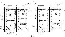
图1,是模式性地表示本发明的第1实施方式中的液晶装置100的概略构成的平面图。在图1中,在纸面跟前侧(观看侧)配置滤色器基板92,另一方面在纸面进深侧则配置元件基板91。还有,在图1中,将纸面纵向方向(列方向)规定为Y方向,并且,将纸面横向方向(行方向)规定为X方向。另外,在图1中,分别对应于红色(R)、绿色(G)、蓝色(B)、任意的色(Other,在以下,有时简记为“O”)的4色的区域表示1个子像素区域SG,并且通过R、G、B、O的各色的子像素区域SG所构成的2行2列的像素排列,表示1个像素区域AG。各子像素区域SG,形成为大致正方形,成为具有相同的面积的区域。还有,在以下,有时也将存在于1个子像素区域SG内的1个显示区域称为“子像素”,并且,将对应于1个像素区域AG内的显示区域称为“单位像素”。FIG. 1 is a plan view schematically showing a schematic configuration of a
液晶装置100,通过框状的密封材料5而贴合元件基板91,和对向于该元件基板91所配置的滤色器基板92,在以该密封材料5所划分的区域内封入液晶而形成液晶层4。The
在此,液晶装置100,是采用R、G、B、O的4色所构成的彩色显示用的液晶装置;并且是采用了在后述的第1基板上以600℃以下的温度所制造、具有双栅结构的LTPS(低温多晶硅)型的TFT元件(以下,称为“LTPS型TFT元件21”)作为开关元件的有源矩阵驱动方式的液晶装置。并且,该液晶装置100,是在形成有像素电极等的各种电极的元件基板91侧,在与该元件基板91面大致平行的方向及大致垂直的方向(观看侧)使边缘场(电场E)发生而对液晶分子的取向进行控制的,所谓的FFS方式的液晶装置。因此,可以在该液晶装置100中得到高的视场角等。另外,液晶装置100,是仅进行透射型显示的透射型的液晶装置。Here, the
首先,元件基板91的平面构成如下。First, the planar configuration of the
在元件基板91的内面上,主要形成或安装:多条源线32,多条栅线33,多个LTPS型TFT元件21,多个像素电极10,共用电极20,信号线驱动电路40,扫描线驱动电路41,外部连接用布线35及FPC(FlexiblePrinted Circuit,柔性印刷电路)等的安装部件42等。On the inner surface of the
如示于图1中地,元件基板91,具有从滤色器基板92的相邻的二边侧向各自的外侧伸出的伸出区域36,在为滤色器基板92的一边侧的外侧且位于Y方向的伸出区域36上安装信号线驱动电路40;并在为滤色器基板92的其他的一边侧的外侧且位于X方向的伸出区域36上安装扫描线驱动电路41。信号线驱动电路40及扫描线驱动电路41的各输入侧的端子(图示略),与多条外部连接用布线35的一端侧电连接,并且多条外部连接用布线35的另一端侧与安装部件42电连接。还有,在图1中,为了方便,对扫描线驱动电路41和安装部件42通过了外部连接用布线35的连接状态的图示进行省略。As shown in FIG. 1 , the
各源线32,形成为在X方向隔开适宜的间隔而延伸于Y方向,各源线32的一端侧,电连接于信号线驱动电路40的输出侧的端子(图示略)。The source lines 32 are formed to extend in the Y direction at appropriate intervals in the X direction, and one end side of each
各栅线33,例如,具有Ti(钛)/Al(铝)/Ti(钛)的3层结构,并形成为在Y方向隔开适宜的间隔而延伸于X方向且延伸于有效显示区域V内。各栅线33的一端侧,电连接于扫描线驱动电路41的输出侧的端子(图示略)。Each
在各源线32和各栅线33的交叉位置附近对应设置LTPS型TFT元件21,LTPS型TFT元件21电连接于各源线32、各栅线33及各像素电极10等。LTPS
各像素电极10,例如通过ITO等的透明导电材料所形成,对应于各子像素区域SG内所设置。Each
共用电极20,通过与像素电极10相同的材料所形成,具有与有效显示区域V大致相同的大小的区域(以粗的虚线所包围的区域),并夹着示于图3中的第3绝缘膜(电介质膜)53而大致整面状地设置于各像素电极10的下侧。共用电极20,通过由与该共用电极20相同的材料等所构成的共用布线27,例如,与信号线驱动电路40内的共用电位用端子(COM端子)电连接。The
1个像素区域AG在X方向及Y方向有多个、其排列成矩阵状的区域是有效显示区域V(通过双点划线所包围的区域)。在该有效显示区域V,显示文字、数字、图形等的图像。还有,有效显示区域V的外侧的区域成为不用于显示的框缘区域38。并且,在各像素电极10等的内面上,形成未图示的取向膜。该取向膜,按预定的方向R实施了摩擦处理(参照图2)。One pixel area AG has a plurality of pixel areas AG in the X direction and the Y direction, and the area in which these are arranged in a matrix is the effective display area V (area surrounded by double-dashed lines). In this effective display area V, images of characters, numerals, figures, and the like are displayed. In addition, an area outside the effective display area V becomes a
其次,滤色器基板92的平面构成如下。Next, the planar configuration of the
滤色器基板92,如也参照图3而明白地,具有:遮光层(一般称为“黑矩阵”,在以下,简单地记为“BM”),R、G、B、O的4色的着色层6R、6G、6B、6O,外覆层16及取向膜18等。还有,在以下的说明中,不管颜色如何而指着色层的情况下简记为“着色层6”,而区分颜色地指着色层的情况下则记为“着色层6R”等。BM,形成于对各子像素区域SG进行划分的位置等。The
在具有以上的构成的液晶装置100中,基于来自与电子设备等所连接了的安装部件42侧的信号及电力等,通过扫描线驱动电路41,按G1、G2、...、Gm-1、Gm(m:自然数)的顺序依次排他性地逐条选择栅线33,并对所选择了的栅线33,供给选择电压的栅信号,另一方面,对其他的非选择的栅线33,则供给非选择电压的栅信号。然后,信号线驱动电路40,对于存在于与所选择了的栅线33对应的位置的像素电极10,将相应于显示内容的源信号,通过分别相对应的S1、S2、...、Sn-1、Sn(n:自然数)的源线32及各LTPS型TFT元件21而进行供给。其结果,液晶层4的显示状态,转换为非显示状态或中间显示状态,液晶层4内的液晶分子的取向状态受到控制。由此,能够在有效显示区域V内对预期的图像进行显示。In the
(像素构成)(pixel composition)
其次,参照图2(a)及图3等,关于本发明的第1实施方式中的液晶装置100的像素构成等而进行说明。Next, the pixel configuration and the like of the
图2(a),表示第1实施方式中的元件基板91中的1像素的量的平面构成。在图2(a)中,仅图示为了说明元件基板91所需的最小限度的要件。图3,表示沿图2(a)中的剖切线A-A’的剖面图,并且表示在通过LTPS型TFT元件21的位置进行了剖切时的包括1子像素的剖面构成。FIG. 2( a ) shows the planar configuration of one pixel in the
首先,关于第1实施方式的元件基板91中的像素构成等而进行说明。First, the pixel configuration and the like in the
元件基板91,具有将通过配置为2行2列的4个子像素所构成的单位像素配置成矩阵状所构成的有效显示区域V(参照图1)。在此,在单位像素内各子像素,对应于像素电极10和共用电极20平面性地相重合的电极部分,设定为该各子像素具有大致相同的面积。The
在为玻璃基板的第1基板1的内面上,对应于源线32和栅线33的交叉位置,形成对于栅线33两次相交叉地具有大致U状的平面形状的低温型的P-Si(多晶硅)层19。在P-Si层19及第1基板1的内面上,遍布其大致一面,形成例如由SiO2等构成的栅绝缘膜50。On the inner surface of the
栅绝缘膜50,在P-Si层19的一端侧且与源线32的一部分平面性地相重叠的位置具有第1接触孔50a,并在对应于P-Si层19的另一端侧的位置具有第2接触孔50b。在栅绝缘膜50的内面上形成栅线33,该栅线33,如示于图2(a)中地,形成为在Y方向上隔开一定的间隔而延伸于X方向,而且与P-Si层19部分性且平面性地相重叠。还有,在后述的源线32的延伸方向相邻的子像素的间隔,比在栅线33的延伸方向相邻的子像素的间隔大。The
在栅线33及栅绝缘膜50的内面上,形成例如由SiO2等构成的透明的第1绝缘膜51。第1绝缘膜51,在对应于第1接触孔50a的位置具有第1接触孔51a,并在对应于第2接触孔50b的位置具有第2接触孔51b。在第1绝缘膜51的内面上,设置源线32及中继电极77。On the inner surfaces of the
源线32,如示于图2(a)中地,形成为在X方向上隔开一定的间隔而延伸于Y方向。源线32的一部分,与P-Si层19的一端侧的一部分平面性地相重叠。源线32的一部分,设置为进入到第1接触孔50a及51a内,该源线32,与P-Si层19的一端侧电连接。中继电极77,与P-Si层19的另一端侧的一部分平面性地相重合。中继电极77的一部分,设置为进入到第2接触孔50b及51b内,该中继电极77,与P-Si层19的另一端侧电连接。由此,各源线32,通过相对应的各P-Si层19,电连接于相对应的各中继电极77。如此一来,在对应于各P-Si层19的位置且对应于源线32和栅线33的交叉位置而设置双栅结构的LTPS型TFT元件21。The source lines 32 are formed to extend in the Y direction at regular intervals in the X direction as shown in FIG. 2( a ). A part of the
在源线32、中继电极77及第1绝缘膜51的内面上,形成例如由透明的丙烯酸树脂等构成的第2绝缘膜52。第2绝缘膜52的内面上具有平坦性,第2绝缘膜52构成平坦化膜。第2绝缘膜52,在中继电极77的一端侧且第2接触孔50b及51b的附近位置具有接触孔52a。还有,在本发明中,在第1绝缘膜51和第2绝缘膜52之间,也可以进一步设置例如由SiNX(氮化硅膜)等构成的绝缘膜。On the inner surfaces of the
在第2绝缘膜52的内面上,遍布其大致一面,形成电连接于COM端子(共用电位用端子)的共用电极20(也参照图1)。共用电极20,例如通过ITO等的透明导电材料所形成,在对应于接触孔52a的位置具有开口20a。在位于接触孔52a内的第2绝缘膜52的一部分及共用电极20的内面上,形成例如由SiO2、SiNX等构成的第3绝缘膜53。第3绝缘膜53,在对应于第2绝缘膜52的接触孔52a的位置具有接触孔53a。第3绝缘膜53,因为设置于共用电极20和后述的像素电极10之间,所以作为形成辅助电容的电介质膜而发挥作用。在此,为了确保足够的辅助电容,优选:第3绝缘膜53的厚度d1,尽可能薄地设定。On the inner surface of the second insulating
为了实现该目的,在合适的例中,第3绝缘膜53的厚度d1,优选确定为:形成于自身的辅助电容的大小设定为约100~600fF,更理想为约200~800fF。并且,在精细度200PPi以上时,优选第3绝缘膜53的厚度d1设定为约50~400nm;另一方面若精细度不足200PPi,则优选第3绝缘膜53的厚度d1设定为约200~1000nm。In order to achieve this purpose, in a suitable example, the thickness d1 of the third insulating
在为第3绝缘膜53的内面上的、各子像素区域SG内,形成通过例如ITO等的透明导电材料形成的像素电极10。各像素电极10,对应于各子像素区域SG的形状形成为大致正方形,在单位像素内,各子像素中的各像素电极10的面积分别设定为相同的大小。像素电极10,设置为进入到接触孔52a及53a内,通过该接触孔52a及53a与中继电极77电连接。因此,来自源线32的源信号(图像信号),通过LTPS型TFT元件21及中继电极77向像素电极10所供给。并且,像素电极10,通过第3绝缘膜53而与共用电极20相对向且平面性地相重叠。在像素电极10,设置用于在自身和共用电极20之间、使边缘场(电场E)发生的多个缝隙10x。各缝隙10x,形成为细长状且横条状的形状,各缝隙10x的长边10xa的延伸方向,规定为与子像素的排列的列方向及源线32的延伸方向不相同的方向。在本例中,各缝隙10x的长边10xa的延伸方向,规定为相对于子像素的排列的行方向及栅线33的延伸方向仅倾斜了预定的角度的方向。但是,在本发明中,各缝隙10x的长边10xa的延伸方向,也可以规定为与子像素的排列的行方向及栅线33的延伸方向相同的方向。还有,虽然在本例中,与各缝隙10x的长边10xa相关联的该各缝隙10x的短边(符号进行省略)形成为具有曲线状的形状,但是并不限于此,在本发明中,并不限定该短边的形状,例如也可以形成为直线状的形状。In each sub-pixel region SG, which is the inner surface of the third insulating
在第3绝缘膜53的一部分及像素电极10的内面上形成未图示的取向膜。对该取向膜,如示于图2(a)中地,按栅线33的延伸方向(以下,称为“摩擦方向R”)实施摩擦处理。因此,液晶分子4a,在初始取向状态下,以其长轴方向沿摩擦方向R的状态进行取向。并且,在第1基板1的下侧设置偏振板11,并在偏振板11的下侧设置作为照明装置的背光源15。如此一来,构成包括第1实施方式中的像素构成的元件基板91。An alignment film (not shown) is formed on a part of the third insulating
另一方面,对应于上述的像素构成的滤色器基板92的构成如下。On the other hand, the configuration of the
在为玻璃基板的第2基板2的内面上的1个像素区域AG内,按子像素区域SG的每个,设置由任意的色的着色层,例如红色(R)的着色层6R、绿色(G)的着色层6G、蓝色(B)的着色层6B、及任意色(O)的着色层6O之中的,任何一色构成的着色层6。还有,在本发明中,并不限定于:对于配置为2行2列的各子像素的,红色(R)、绿色(G)、蓝色(B)、任意色(O)的着色层6的排列顺序,该各色的着色层6的排列顺序是任意的。在为第2基板2的内面上的、对各子像素区域SG进行划分的位置及对应于LTPS型TFT元件21的位置,设置BM。因此,LTPS型TFT元件21、源线32及栅线33等与BM平面性地相重叠。在BM及各着色层6的内面上形成外覆层16。该外覆层16,具有保护着色层6等不被在液晶装置100的制造工序中所使用的药剂等腐蚀、污染的功能。在外覆层16的内面上形成按预定的方向实施了摩擦处理的取向膜18。如此一来,构成第1实施方式中的滤色器基板92。In one pixel region AG on the inner surface of the
在具有以上的构成的液晶装置100中,在其驱动时,沿摩擦方向R处于初始取向状态下的液晶分子(图示略),通过产生于源线32的延伸方向的边缘场(电场E)逆时针旋转或顺时针旋转而在源线32的延伸方向上进行重取向。还有,在图3的剖面构成中,边缘场(电场E),在与元件基板91大致平行的方向(纸面横向方向)及大致垂直的方向(滤色器基板侧)上具有强的电场分量,并通过该多个缝隙10x及第3绝缘膜53而在像素电极10和共用电极20之间产生。由此,液晶分子的取向状态得到控制,能够进行透射型显示。而且,在透射型显示时,从背光源15出射出来的照明光,沿示于图3中的路径T而行进,并通过共用电极20,像素电极10及R、G、B、O的各着色层6等而到达观看者。该情况下,该照明光,通过对该着色层6等进行透射而呈现预定的色调及亮度。如此一来,通过观看者而识别预期的彩色显示图像。In the
(电等效电路的构成)(Constitution of electrical equivalent circuit)
其次,参照图5等,关于第1实施方式中的液晶装置100的电等效电路的构成进行说明。图5,是表示液晶装置100的电等效电路的构成的框图。还有,虽然在图5中,实际上,扫描线驱动电路41和安装部件42通过外部连接用布线35相连接,但是为了方便,其图示进行省略。Next, the configuration of the electrical equivalent circuit of the
液晶装置100,具有:使设置于1个像素区域AG内的单位像素(以下,称为“单位像素P”)矩阵状地排列于行方向(X方向)及列方向(Y方向)的有效显示区域V,设置于其外侧、对设置于各子像素区域SG内的各子像素(以下,称为“子像素SP”)进行驱动的信号线驱动电路40及扫描线驱动电路41,和与信号线驱动电路40及扫描线驱动电路41电连接、为液晶装置100和电子设备的接口的安装部件42。The
液晶装置100,具备:每隔预定间隔交替设置的多条栅线33及公共线80,和每隔预定间隔地设置而与栅线33及公共线80交叉的多条源线32。The
单位像素P,通过配置为2行2列的4个子像素SP所构成。若换言之,则在单位像素P内,4个子像素SP的排列状态,变成在源线32的延伸方向(Y方向)为2列,及,在栅线33的延伸方向(X)方向为2行。各子像素SP,对应于各栅线33及各公共线80和各源线32的交叉位置所设置。还有,在本发明中,如上述地,因为在设置于像素电极10和共用电极20之间的作为电介质膜的第3绝缘膜53形成辅助电容,所以不必设置公共线80及后述的存储电容81。The unit pixel P is constituted by four sub-pixels SP arranged in two rows and two columns. In other words, in the unit pixel P, the arrangement state of the four sub-pixels SP becomes 2 columns in the extending direction (Y direction) of the
至少在各子像素区域SG内,设置:LTPS型TFT元件21,像素电极10,夹着第3绝缘膜53(图示略)对向于该像素电极10的共用电极20,以及电连接于像素电极10及公共线80的存储电容81。At least in each sub-pixel region SG, an LTPS
在LTPS型TFT元件21的栅电极,连接栅线33;在LTPS型TFT元件21的源电极,连接源线32;在LTPS型TFT元件21的漏电极,连接像素电极10及存储电容81。在像素电极10和共用电极20之间,夹持液晶层4。从而,该LTPS型TFT元件21,若从栅线33施加选择电压,则使源线32和像素电极10及存储电容81为导通状态。The gate electrode of the
扫描线驱动电路41,对各栅线33按线顺序供给使LTPS型TFT元件21成为导通状态的选择电压。例如,若对某栅线33供给选择电压,则连接于该栅线33的LTPS型TFT元件21全部变成导通状态,与该栅线33有关的子像素SP的全部被选择。具体地,扫描线驱动电路41,具有移位寄存器电路41a、输出控制电路41b及缓冲电路41c,并对该扫描线驱动电路41,通过安装部件42,从未图示的电子设备的外部电路侧供给电力及各种的信号。移位寄存器电路41a,是顺序传送型移位寄存器,若从电子设备的外部电路侧供给起始信号VSP(1帧的开始信号)、时钟信号VCK、及方向信号VDIR(指定栅线的扫描方向的信号)等的各种信号,则将这些各种信号向输出控制电路41b进行输出。输出控制电路41b,是对扫描线驱动电路41的工作进行控制的电路,当从电子设备的外部电路内的电源电路所供给的驱动信号VENB为L(低)电平时,将可以对栅线33进行选择的控制信号向缓冲电路41c进行输出,并将从移位寄存器电路41a输出出来的起始信号VSP、时钟信号VCK及方向信号VDIR等的各种信号向缓冲电路41c进行输出。缓冲电路41c,是进行从输出控制电路41b输出出来的各种信号的波形整形的波形整形用电路。还有,在本发明中,在输出控制电路41b和缓冲电路41c之间,也可以设置对从输出控制电路41b输出出来的各种信号的电平进行放大的电平移位(level shifter)电路。具有以上的构成的扫描线驱动电路41,在一垂直扫描期间(1V期间)内,对地址序号G1、G2、...、Gm-1、Gm的栅线33(也参照图1)按顺序进行扫描,并在一水平扫描期间(1H期间)内对2条栅线33按顺序进行扫描而对单位像素P进行驱动。The scanning
信号线驱动电路40,将图像信号供给于各源线32,并通过导通状态的LTPS型TFT元件21,对各子像素区域SG内的像素电极10按顺序写入图像信息。具体性地,信号线驱动电路40,具备对应于各单位像素P的列所设置的作为解复用器的解复用器单位电路310,各解复用器单位电路310,包括一对传输门(transfer gate)311及312所构成。解复用器单位电路310,具有以下功能:将通过安装部件42从电子设备的外部电路(图示略)所供给的时分信号,通过将传输门311及312进行电开闭,向对应的单位像素P中的源线32进行分配。还有,在本发明中,不是必须在信号线驱动电路40内设置解复用器单位电路310。该情况下,各源线32,变成直接与信号线驱动电路40电连接的构成。The signal
具有以上的构成的液晶装置100,如以下地进行工作。The
即,通过从扫描线驱动电路41按线顺序供给选择电压,对与某栅线33相连接的子像素SP的全部进行选择。然后,同步于这些子像素SP的选择,从信号线驱动电路40将图像信号供给于源线32。由此,对以扫描线驱动电路41及信号线驱动电路40进行了选择的全部的子像素SP,从源线32通过LTPS型TFT元件21供给图像信号,图像信息被写入像素电极10。That is, all of the sub-pixels SP connected to a
若对子像素区域SG内的像素电极10写入图像信息,则通过该像素电极10和共用电极20的电位差,对液晶层4施加驱动电压。从而,通过使图像信号的电压电平发生变化,使液晶的取向、秩序发生变化,进行通过各子像素SP的光调制产生的灰度等级显示。When image information is written to the
还有,施加于液晶的驱动电压,通过存储电容81,保持比写入图像信息的期间长3位的期间。In addition, the drive voltage applied to the liquid crystal is held by the storage capacitor 81 for a period longer than the period for writing the image information by 3 bits.
图6,是表示有效显示区域V内的任意的单位像素P,及对应于该任意的单位像素P的解复用器单位电路310的电构成的电路图。FIG. 6 is a circuit diagram showing an arbitrary unit pixel P in the effective display area V and an electrical configuration of a
在此,在图6中,为了说明的方便,将位于上侧的栅线33作为“栅线33a”,并且,将位于下侧的栅线33作为“栅线33b”。对栅线33a及栅线33b,分别供给扫描信号GATE1a、1b。并且,在图6中,为了说明的方便,将位于左侧的源线32作为“源线32a”,并且,将位于右侧的源线32作为“源线32b”。对公共线80及共用电极20供给驱动信号VCOM。Here, in FIG. 6 , for convenience of description, the
解复用器单位电路310,是1输入2输出型的1∶2解复用器,相对于1个输入端子SEG具有2个输出端子SS1、SS2,并通过将从2个输出端子SS1、SS2之中选择出来的输出端子连接于输入端子SEG,而将作为时分信号所供给的图像信号分配给源线32a、32b。The
解复用器单位电路310,例如,具有以为互补型晶体管的CMOS(Complementary Metal-Oxide Semiconductor,互补型金属氧化物半导体)所构成的第1传输门311及第2传输门312。具体性地,第1传输门311及第2传输门312的一方的端子,连接于输入端子SEG;其他方的端子,分别连接于输出端子SS1及SS2。The
输出端子SS1,连接于分别与红色(R)及蓝色(B)的各子像素SP相连接的源线32a。另一方面,输出端子SS2,连接于分别与绿色(G)及任意色(O)的各子像素SP相连接的源线32b。The output terminal SS1 is connected to the source line 32a connected to the red (R) and blue (B) sub-pixels SP, respectively. On the other hand, the output terminal SS2 is connected to the source line 32b connected to each sub-pixel SP of green (G) and any color (O).
对第1传输门311的控制端子,输入选择信号SEL1、SEL1B。选择信号SEL1B,是使选择信号SEL1反相后的信号。若选择信号SEL1、SEL1B变成有效,则第1传输门311变成导通状态,将从输入端子SEG所输入进来的图像信号向源线32a供给。The selection signals SEL1 and SEL1B are input to the control terminals of the
对第2传输门312的控制端子,输入选择信号SEL2、SEL2B。选择信号SEL2B,是使选择信号SEL2反相后的信号。若选择信号SEL2、SEL2B变成有效,则第2传输门312变成导通状态,将从输入端子SEG所输入进来的图像信号向源线32b供给。To the control terminal of the
对输入端子SEG,输入红色(R)、绿色(G)、蓝色(B)、任意色(O)的各色的图像信息的复用信号。A multiplexed signal of image information of each color of red (R), green (G), blue (B), and any color (O) is input to the input terminal SEG.
以上的解复用器单位电路310,如以下地进行工作。The
对输入端子SEG供给图像信号,并使选择信号SEL1、SEL1B,或者,选择信号SEL2、SEL2B为有效。由此,能够对连接于红色(R)及蓝色(B)的各子像素的源线32a,或者,对连接于绿色(G)及任意色(O)的各子像素的源线32b进行选择,对该所选择的源线32供给图像信号。An image signal is supplied to the input terminal SEG, and selection signals SEL1, SEL1B, or selection signals SEL2, SEL2B are asserted. Thus, the source line 32a connected to each sub-pixel of red (R) and blue (B), or the source line 32b connected to each sub-pixel of green (G) and any color (O) can be is selected, and the image signal is supplied to the selected
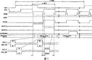
其次,参照图7,关于液晶装置100的驱动方法进行说明。图7,表示液晶装置100的驱动方法中的时序图。Next, a method of driving the
如上述地,VSP为起始信号,VCK为时钟信号,这些起始信号VSP及时钟信号VCK,通过扫描线驱动电路41供给于液晶装置100。并且,VENB为驱动信号,当该驱动信号VENB为L电平时,扫描线驱动电路31,变得可以选择供给到栅线33的扫描信号GATE1a、1b、2a、2b、...、640a、640b(例如,栅线33的条数为1280条的情况)。As described above, VSP is a start signal, and VCK is a clock signal, and these start signal VSP and clock signal VCK are supplied to the
另外,VDIR为指定扫描方向的信号,该方向信号VDIR,在第1实施方式中,总是为H(高)电平,从图5中左侧向右侧进行扫描。In addition, VDIR is a signal specifying the scanning direction. In the first embodiment, the direction signal VDIR is always at H (high) level, and scanning is performed from left to right in FIG. 5 .
VCOM,如上述地,是供给于共用电极20及公共线80的驱动信号。在第1实施方式中,采用按每1行使共用电极20的电位反相的行反相驱动方式,VCOM,按每1行进行反相。VCOM is a driving signal supplied to the
GATE,如上述地,是供给于栅线33的扫描信号。在第1实施方式中,栅线33的条数例如为1280条,在图6中,GATE1a,在有效显示区域V内,为供给于最上级的栅线33a的扫描信号;GATE1b,则为供给于最上级的下一级的栅线33b的扫描信号。GATE640b,在有效显示区域V内,为供给于最下级的栅线33b的控制信号。GATE is a scanning signal supplied to the
DISPLAY DATA信号,为供给于信号线驱动电路40的时分的图像信号。The DISPLAY DATA signal is a time-division image signal supplied to the signal
在此,当着眼于1H期间时,VCOM及VENB分别为L电平的状态,从时刻t1到t2之间,GATE1a变成H电平,在单位像素P内,选择与最上级的栅线33a相关的、红色(R)及绿色(G)的各子像素SP。并且,同步于这些各子像素SP的选择,作为DATA,红色(R)及绿色(G)的图像信息V001连续地供给于解复用器单位电路310。供给红色(R)的图像信息V001的期间,选择信号SEL1、SEL1B有效,而选择信号SEL2、SEL2B无效。并且,供给绿色(G)的图像信息V001的期间,选择信号SEL1、SEL1B无效,而选择信号SEL2、SEL2B有效。Here, when focusing on the 1H period, VCOM and VENB are in the state of L level, and GATE1a becomes H level from time t1 to t2, and in the unit pixel P, the
由此,红色(R)的图像信息V001,通过源线32a,供给于与最上级的栅线33a有关的红色(R)的子像素SP;绿色(G)的图像信息V001,通过源线32b,供给于与最上级的栅线33a有关的绿色(G)的子像素SP。Thus, the red (R) image information V001 is supplied to the red (R) sub-pixel SP related to the
接着,仅从时刻t2到t3之间VENB变成H电平,进而VCOM发生反相而变成H电平的状态,若在时刻t3、VENB从H电平向L电平下降,则同步于此从时刻t3到t4之间,GATE1b变成H电平,在有效显示区域V内,选择与最上级的下一级的栅线33b有关的、蓝色(B)及任意色(O)的各子像素SP。并且,同步于这些各子像素SP的选择,作为DATA,蓝色(B)及任意色(O)的图像信息V001连续地供给于解复用器单位电路310。供给蓝色(B)的图像信息V001期间,选择信号SEL1、SEL1B有效,而选择信号SEL2、SEL2B无效。并且,供给任意色(O)的图像信息V001期间,选择信号SEL1、SEL1B无效,而选择信号SEL2、SEL2B有效。Next, only from the time t2 to t3, VENB becomes H level, and then VCOM is reversed to become H level state. From the time t3 to t4, GATE1b becomes H level, and in the effective display area V, the blue (B) and any color (O) related to the
由此,蓝色(B)的图像信息V001,通过源线32a,供给于与最上级的下一级的栅线33b有关的蓝色(B)的子像素SP;任意色(O)的图像信息V001,通过源线32b,供给于与最上级的下一级的栅线33b有关的任意色(O)的子像素SP。Thus, the blue (B) image information V001 is supplied to the blue (B) sub-pixel SP related to the
在1V期间内进而直到对应于图像信息V640的GATE640a、GATE640b为止地进行以上叙述的驱动控制。The drive control described above is further performed up to GATE640a and GATE640b corresponding to the image information V640 within the period of 1V.
如以上地,在该液晶装置100中,采用以下的驱动方法:在单位像素P中,在1H期间,按顺序扫描(2次扫描)位于同一行方向的2个子像素SP,通过对应于该各自的子像素SP的各源线32来供给图像信号。As described above, in the
其次,关于与比较例进行了比较的、第1实施方式中的液晶装置100的特有的作用效果而进行说明。Next, a description will be given of the unique effects of the
在以下,首先,参照图8(a)及(b),关于比较例中的FFS方式的液晶装置500的元件基板91x的构成及其问题点而进行说明,其后,关于与比较例进行了比较的第1实施方式的特有的作用效果而进行说明。还有,在比较例中,关于与第1实施方式相同的要件附加相同的符号,且其说明进行简化或省略。In the following, first, the configuration and problems of the
图8(a),表示对应于图2(a)的、比较例中的元件基板91x中的1像素量的平面构成。图8(b),表示沿图8(a)的剖切线C-C’的、元件基板91x中的1子像素的剖面构成。还有,比较例的各子像素区域SG1,与第1实施方式的子像素区域SG不同,是在子像素的排列的列方向具有长边,并在其行方向具有短边的纵长区域,各子像素区域SG1的长边的方向,规定为源线32的延伸方向;另一方面,各子像素区域SG的短边的方向,则规定为栅线33的延伸方向。FIG. 8( a ) shows a planar configuration corresponding to one pixel of an
比较例中的液晶装置500,在作为开关元件而具有α-Si型TFT元件23的元件基板91x,和未图示的滤色器基板92之间封入液晶而形成液晶层4。In a liquid crystal device 500 in the comparative example, liquid crystal is sealed between an
首先,元件基板91x的构成如下。First, the configuration of the
在比较例中,单位像素,通过包括红色(R)、绿色(G)、蓝色(B)、其他色(O)的4色的配置为1行4列的多个子像素所构成。还有,比较例中的1个像素区域AG的面积,规定为与第1实施方式中的1个像素区域AG的面积相同的大小。In the comparative example, a unit pixel is constituted by a plurality of sub-pixels arranged in one row and four columns of four colors including red (R), green (G), blue (B), and other colors (O). In addition, the area of one pixel region AG in the comparative example is set to be the same size as the area of one pixel region AG in the first embodiment.
在第1基板1上,按子像素区域SG1的每一个设置由ITO等构成的共用电极20(以双点划线所包围的区域)。共用电极20,形成为在子像素区域SG的行方向(短边方向)具有短边并在子像素区域SG的列方向(长边方向)具有长边的、纵长状的长方形(竖条形状)。在共用电极20的一部分上及第1基板1上,如示于图8(a)中地,设置在Y方向上隔开一定的间隔所形成、而延伸于X方向的共用电极线20s。因此,共用电极20,电连接于共用电极线20s。共用电极线20s,虽然对图示进行省略但是在元件基板91x上的预定位置、与共用电位用端子(COM端子)电连接。在第1基板1上,在Y方向上隔开一定的间隔、延伸于X方向地设置栅线33。栅线33,设置于对应于相邻的单位像素所设置的共用电极线20s的附近位置。On the
在共用电极20、共用电极线20s、栅线33及第1基板1之上,形成栅绝缘膜50。在为栅绝缘膜50上且为后述的源线32与栅线33的交叉位置附近,设置成为α-Si型TFT元件23的要件的α-Si层26。A
在图8(a)中,在栅绝缘膜50上,延伸于Y方向地设置源线32。源线32,具有重叠于α-Si层26上地弯曲、与该α-Si层26电连接的弯曲部分32x。并且,在α-Si层26及栅绝缘膜50上,设置漏电极34。因此,漏电极34,与α-Si层26电连接。因此,源线32的弯曲部分32x,通过α-Si层26电连接于漏电极34。如此一来,在该区域形成α-Si型TFT元件23。In FIG. 8( a ), the
在栅绝缘膜50及α-Si型TFT元件23上,形成例如由SiNx等构成的钝化层54。钝化层54,在与共用电极20的一部分相重叠的位置且与漏电极34的一端侧相重叠的位置具有接触孔54a。On the
在钝化层54上,按子像素区域SG1的每个形成由ITO等构成的像素电极10。像素电极10,形成为在子像素的排列的行方向具有短边10S并在子像素的排列的列方向具有长边10L的、纵长状的长方形(竖条形状)。像素电极10,具有多个缝隙10x,并且各缝隙10x,形成为细长状且延伸于子像素的排列的行(横向)方向而构成横条状,并且各缝隙10x的长边10xa的延伸方向,规定为相对于像素电极10的短边10S的延伸方向及栅线33的延伸方向仅倾斜了预定的角度的方向。像素电极10,通过接触孔54a电连接于漏电极34。因此,对像素电极10,通过α-Si型TFT元件23而供给来自源线32的源信号(图像信号)。在像素电极10等之上形成未图示的取向膜。对该取向膜,按与第1实施方式同样的方向实施摩擦处理。On the
在具有以上的构成的比较例中的液晶装置500中,在其驱动时,通过与第1实施方式中的液晶装置100同样的原理而控制液晶的取向,进行透射型显示。In the liquid crystal device 500 of the comparative example having the above-mentioned configuration, when the liquid crystal device 500 is driven, the orientation of the liquid crystal is controlled by the same principle as that of the
在具有如此的构成的比较例中,具有如下的问题。In the comparative example having such a configuration, there were the following problems.
即,在比较例中,如示于图8(a)中地,将像素电极10形成为竖条形状,将其各缝隙10x规定为相对于像素电极10的短边10S的延伸方向且栅线33的延伸方向仅倾斜了预定的角度的方向。因此,在比较例中,因为需要遍布像素电极10的整体而均匀地设置缝隙10x,所以在其结构上,增加了缝隙10x的设定数。在此,在像素电极10的各缝隙10x的长边10xa的方向的两端部之中的任何一方的端部附近,与不是各缝隙10x的端部附近的位置相比较,而边缘场(电场E)的施加方式改变,发生液晶分子几乎得不到驱动的畴区域(液晶的取向异常区域)DAr。因此,在该畴区域DAr中,明亮度降低而变成显示上暗的区域。还有,该畴区域DAr,从现象上看,按缝隙10x的设定数发生,并且,在相邻于Y方向的各缝隙10x之间互不相同且锯齿状地发生。从而,存在下述问题:如比较例地设置于像素电极10的缝隙10x的数越多则不用于明亮度的畴区域DAr就越增加,而相应地,液晶装置的透射率显著地降低。That is, in the comparative example, as shown in FIG. 8( a), the
从而,若能对像素结构下工夫,而尽可能地减少设置于子像素(像素电极10)的缝隙10x的设定数,则能够将显示状态保持为适当的状态且减少畴区域DAr,能够改善如上述的问题。Therefore, if the number of
于是,在第1实施方式中,首先,将单位像素,通过配置为2行2列的4个子像素而构成。然后,将对应于子像素的像素电极10的形状形成为大致正方形状,并在各像素电极10,按子像素区域SG每一个设置多个缝隙10x,使各缝隙10x,细长状且延伸于子像素的排列的行(横向)方向地形成,将各缝隙10x的长边10xa的延伸方向,规定为与子像素的排列的列方向及源线32的延伸方向不相同的方向。在本例中,将各缝隙10x的长边10xa的延伸方向,规定为相对于子像素的排列的行方向及栅线33的延伸方向仅倾斜了预定的角度的方向。但是,在本发明中,也可以将各缝隙10x的长边10xa的延伸方向,规定为与子像素的排列的行方向及栅线33的延伸方向相同的方向。Therefore, in the first embodiment, first, a unit pixel is configured by arranging four sub-pixels in two rows and two columns. Then, the shape of the
由此,在像素电极10的整体均匀地配置缝隙10x,且与比较例相比较,能够减少该缝隙10x的设定数。例如,相对于在比较例中,设置于各子像素的缝隙10x的设定数为11个,而在第1实施方式中,设置于各子像素的缝隙10x的设定数变成了7个。虽然在具有如此的构成的第1实施方式中,在液晶的驱动时,如示于图2(a)中地,在各缝隙10x的长边10xa的方向的两端部之中的任何一方的端部附近产生畴区域DAr,但是因为与比较例相比较而减少了设定于像素电极10的缝隙10x的数目,所以伴随于此能够减少畴区域DAr。其结果,能够防止液晶装置100的透射率降低。Thereby, the
并且,在第1实施方式中,如示于图2(a)中地,将设置于像素电极10的缝隙10x的长边10xa的延伸方向,规定为与子像素的排列的行方向及栅线33的延伸方向大致相同的方向。因此,在液晶的驱动时在像素电极10和共用电极20之间产生的边缘场(电场E),产生于源线32的延伸方向上。但是,在第1实施方式中,因为相邻于源线32的延伸方向的子像素的间隔,比相邻于栅线33的延伸方向的子像素的间隔大,所以当着眼于相邻于源线32的延伸方向的任意的子像素时,产生于该一方的子像素的边缘场(电场E)并不影响到另一方的子像素,不会使该其他的子像素中的液晶分子不必要地进行工作。即,若采用该缝隙结构,则在相邻于源线32的延伸方向的任意的子像素间,能够防止该各自中产生的边缘场(电场E)相互受到影响。从而,因为作为该次要的效果,难以在对应于源线32的位置处产生液晶的取向紊乱,所以在滤色器基板92侧,也可以在对应于该源线32的位置处不设置BM。In addition, in the first embodiment, as shown in FIG. 2( a ), the extending direction of the long side 10xa of the
并且,在第1实施方式中,通过如上述地配置为2行2列的4个子像素而构成单位像素,在该单位像素中,对应于第1行中的2个子像素的2个像素电极10(即,第1行第1列的子像素中的像素电极10及第1行第2列的子像素中的像素电极10),电共用连接于1条栅线33;并且对应于第2行中的2个子像素的2个像素电极10(即,第2行第1列的子像素中的像素电极10及第2行第2列的子像素中的像素电极10),电共用连接于另外的1条栅线33。并且,在该单位像素中,对应于第1列中的2个子像素的2个像素电极10(即,第1行第1列的子像素中的像素电极10及第2行第1列的子像素中的像素电极10),电共用连接于1条源线32;并且对应于第2列中的2个子像素的2个像素电极10(即,第1行第2列的子像素中的像素电极10及第2行第2列的子像素中的像素电极10),电共用连接于另外的1条源线32。因此,在第1实施方式中,在该单位像素中,在1H期间,顺序扫描(2次扫描)位于相同的行方向上的2个子像素,通过对应该各自的子像素的各源线32而供给图像信号。Furthermore, in the first embodiment, a unit pixel is constituted by arranging four sub-pixels in two rows and two columns as described above, and in this unit pixel, two
从而,与上述的比较例中的液晶装置相比较而以2倍的驱动占空比(duty)驱动单位像素的结果,能够谋求显示质量的提高。在此,比较例中的液晶装置,通过配置为1行4列的4个子像素而构成单位像素,在该单位像素中,各子像素电共用连接于1条栅线33,并电连接于相对应的4条源线32的各自。因此,在该液晶装置中,在1H期间内通过1条栅线而扫描单位像素内的4个子像素,该各子像素,通过连接于它们的源线32的各自而被供给图像信号。Therefore, as a result of driving the unit pixel at twice the driving duty compared with the liquid crystal device in the above-mentioned comparative example, the display quality can be improved. Here, the liquid crystal device in the comparative example constitutes a unit pixel by disposing four sub-pixels in one row and four columns. In this unit pixel, each sub-pixel is electrically shared and connected to one
第2实施方式2nd embodiment
其次,参照图2(b)及图4,关于本发明的第2实施方式中的液晶装置200而进行说明。Next, the
图2(b),表示第2实施方式中的元件基板93中的1像素的量的平面构成。还有,在图2(b)中,仅图示用于元件基板91的说明所必需的最小限度的要件。图4,表示沿图2(b)中的剖切线B-B’的剖面图,并表示在通过LTPS型TFT元件21的位置进行了剖切时的包括1子像素的剖面构成。FIG. 2( b ) shows the planar configuration of one pixel in the
在将第2实施方式和第1实施方式中进行了比较的情况下,主要是,该两者在元件基板中相对于作为电介质膜的第3绝缘膜53的、共用电极20和像素电极10的位置关系变得颠倒,而其以外之点该两者则构成上相同。因而,在以下,关于与第1实施方式相同的要件附加相同的符号,对其说明进行简化或省略。When comparing the second embodiment with the first embodiment, it is mainly that the
具体地,与第1实施方式不相同的元件基板93的部分的构成如下。Specifically, the configuration of the part of the
即,第2实施方式,与第1实施方式同样地通过配置为2行2列的4个子像素而构成单位像素,各单位像素内的4个子像素、与栅线33及源线32的连接构成,与第1实施方式是同样的。而且,在元件基板93,在作为平坦化膜的第2绝缘膜54上,按子像素区域SG的每个而具有大致正方形的形状地设置像素电极10。在单位像素内,各子像素中的各像素电极10的面积分别设定为相同的大小。像素电极10与源线32及栅线33的平面性的位置关系与第1实施方式同样。像素电极10,设置得一直进入接触孔52a内,与中继电极77电连接。因此,对像素电极10通过LTPS型TFT元件21而从源线32供给图像信号。在像素电极10及第2绝缘膜52之上,设置作为电介质膜的第3绝缘膜53。在第3绝缘膜53上,整面状地设置共用电极20。共用电极20,按子像素区域SG每个,具有多个缝隙20x,并且各缝隙20x形成为细长状且延伸于子像素的排列的行(横向)方向,各缝隙20x的长边20xa的延伸方向,规定为与子像素的排列的列方向及源线32的延伸方向不相同的方向。在本例中,各缝隙20x的长边20xa的延伸方向,规定为相对于子像素的排列的行方向及栅线33的延伸方向仅倾斜了预定的角度的方向。还有,取代其,在本发明中,各缝隙20x的长边20xa的延伸方向,也可以规定为与子像素的排列的行方向及栅线33的延伸方向相同的方向。还有,虽然在本例中,与各缝隙20x的长边20xa相关联的该各缝隙20x的短边(符号进行省略)形成得具有曲线状的形状,但是并不限于此,在本发明中,并不限定该短边的形状,例如也可以形成为直线状的形状。并且,共用电极20,在子像素区域SG内,在多个缝隙20x之中的位于接触孔52a的附近的缝隙20x的一端侧,具有与该缝隙20x相连的缺口部分20xb。缺口部分20xb,形成得比接触孔52a的面积大,设置于对应于该接触孔52a的位置处。That is, in the second embodiment, a unit pixel is formed by arranging four sub-pixels in two rows and two columns similarly to the first embodiment, and the connection between the four sub-pixels in each unit pixel and the
在具有以上的构成的第2实施方式中,通过配置为2行2列的4个子像素而构成单位像素。而且,对应于子像素的像素电极10,形成为大致正方形。并且,共用电极20,按子像素的每个,具有多个缝隙20x,并且多个缝隙20x形成为细长状且延伸于子像素的排列的行(横向)方向,各缝隙20x的长边20xa的延伸方向,规定为与子像素的排列的列方向及源线32的延伸方向不相同的方向。在本例中,各缝隙20x的长边20xa的延伸方向,规定为相对于子像素的排列的列方向及栅线33的延伸方向仅倾斜了预定的角度的方向。In the second embodiment having the above configuration, a unit pixel is constituted by four sub-pixels arranged in two rows and two columns. Furthermore, the
由此,在共用电极20的整体均匀地配置缝隙20x,且与下述假想的比较例相比较,能够减少该缝隙20x的设定数。在此,该比较例,假想为:具有在上述的比较例中、使像素电极10和共用电极20相对于第3绝缘膜53的位置关系颠倒了的剖面构成,并且设置于共用电极20的缝隙20x形成为细长状且延伸于子像素的排列的行(横向)方向而具有横条形状,并且各缝隙20x的长边20xa的延伸方向,规定为像素电极10的短边10S的延伸方向及栅线33的延伸方向,或规定为相对于该延伸方向仅倾斜了预定的角度的方向。因而,虽然在具有如此的构成的第2实施方式中,在液晶的驱动时,如示于图2(b)中地,在各缝隙20x的长边20xa的方向的两端部之中的任何一方的端部附近产生畴区域DAr,但是因为与该假想的比较例相比较而减少了设定于共用电极20的缝隙20x的个数,所以伴随于此能够减少畴区域DAr。其结果,能够防止液晶装置200的透射率降低。Thereby, the
并且,在第2实施方式中,如示于图2(b)中地,将设置于共用电极20的缝隙20x的长边20xa的延伸方向,规定为与子像素的排列的行方向及栅线33的延伸方向大致相同的方向。因此,在液晶的驱动时在像素电极10和共用电极20之间产生的边缘场(电场E),产生于源线32的延伸方向。但是,在第2实施方式中,因为相邻于源线32的延伸方向的子像素的间隔,与第1实施方式同样地设定得比相邻于栅线33的延伸方向的子像素的间隔大,所以当着眼于相邻于源线32的延伸方向的任意的子像素时,产生于该一方的子像素的边缘场(电场E)并不影响到另一方的子像素,不会使该另外的子像素中的液晶分子不必要地进行工作。即,若采用该缝隙结构,则在相邻于源线32的延伸方向的任意的子像素间,能够防止该各自中产生的边缘场(电场E)相互受到影响。In addition, in the second embodiment, as shown in FIG. 2( b ), the extending direction of the long side 20xa of the
并且,在第2实施方式中,通过如上述地配置为2行2列的4个子像素而构成单位像素,在该单位像素中,对应于第1行中的2个子像素的2个像素电极10与栅线33及源线32的连接构成,以及,对应于第2行中的2个子像素的2个像素电极10与栅线33及源线32的连接构成,具有与上述的第1实施方式同样的构成。因此,在第2实施方式中,在该单位像素中,在1H期间,顺序扫描(2次扫描)位于相同的行方向上的2个子像素,通过对应该各自的子像素的各源线32而供给图像信号。因而,能够得到与上述的第1实施方式同样的作用效果。Furthermore, in the second embodiment, a unit pixel is constituted by arranging four sub-pixels in two rows and two columns as described above, and in this unit pixel, two
(变形例)(Modification)
在上述的第1及第2实施方式中,单位像素内的4个子像素,设定为分别具有大致相同的面积的大小。但是并不限于此,在本发明中,也可以按照需要,为了进行白平衡的调整(色调整),而在单位像素内,采用改变4个子像素的面积的构成。以下,关于该构成例,参照图9及图10进行说明。还有,关于与上述了的第1实施方式相同的要件附加相同的符号,对其说明进行简化或省略。In the first and second embodiments described above, the four sub-pixels in the unit pixel are set to have substantially the same area. However, the invention is not limited thereto, and in the present invention, a configuration may be employed in which the area of four sub-pixels is changed within a unit pixel in order to adjust the white balance (color adjustment) as necessary. Hereinafter, this configuration example will be described with reference to FIGS. 9 and 10 . In addition, the same code|symbol is attached|subjected to the same element as the above-mentioned 1st Embodiment, and the description is simplified or abbreviate|omitted.
图9(a)及图10(a),分别表示对应于图2(a)的像素结构,并表示改变了单位像素内的4个子像素的面积的变形例中的1像素的量的平面结构。图9(b)及图10(b),分别表示对应于图2(b)的像素结构,并表示改变了单位像素内的4个子像素的面积的变形例中的1像素的量的平面结构。Fig. 9(a) and Fig. 10(a) respectively show the pixel structure corresponding to Fig. 2(a), and show the planar structure of 1 pixel in the modified example in which the area of 4 sub-pixels in the unit pixel is changed . Fig. 9(b) and Fig. 10(b) show the pixel structure corresponding to Fig. 2(b) respectively, and show the planar structure of 1 pixel in the modified example in which the area of 4 sub-pixels in the unit pixel is changed .
在示于图9及图10中的变形例中,单位像素,与第1实施方式同样地,通过配置为2行2列的4个子像素所构成。但是,在该变形例中,在单位像素内,在红色(R)的子像素中的像素电极10、绿色(G)的子像素中的像素电极10、蓝色(B)的子像素中的像素电极10、及其他色(O)的子像素中的像素电极10之中,至少1个子像素中的像素电极10的面积,设定为与其他的子像素中的像素电极10的面积不相同的大小。In the modified examples shown in FIGS. 9 and 10 , a unit pixel is constituted by four sub-pixels arranged in two rows and two columns, as in the first embodiment. However, in this modified example, in the unit pixel, the
首先,关于示于图9(a)及图9(b)中的变形例中的像素结构等进行说明。在此,示于图9(a)中的变形例的剖面构成,对应于示于图2(a)中的第1实施方式的剖面构成;而示于图9(b)中的变形例中的剖面构成,则对应于图2(b)中所示的第2实施方式的剖面构成。First, the pixel structure and the like in the modified example shown in FIG. 9( a ) and FIG. 9( b ) will be described. Here, the cross-sectional configuration of the modified example shown in FIG. 9( a) corresponds to the cross-sectional configuration of the first embodiment shown in FIG. 2( a); The cross-sectional configuration corresponds to the cross-sectional configuration of the second embodiment shown in FIG. 2( b ).
在图9(a)及图9(b)中的变形例中,在单位像素内,配置于子像素的排列的相同的列方向(Y方向或纵向方向)上的子像素的各自的面积设定为不相同的大小。具体地,在示于图9(a)及图9(b)中的变形例中,在单位像素内,红色(R)的子像素中的像素电极10和蓝色(B)的子像素中的像素电极10的相对性的面积设定为不相同的大小;并且绿色(G)的子像素中的像素电极10和其他色(O)的子像素中的像素电极10的相对性的面积设定为不相同的大小。In the modified example shown in FIG. 9(a) and FIG. 9(b), in the unit pixel, the respective areas of the sub-pixels arranged in the same column direction (Y direction or vertical direction) of the arrangement of the sub-pixels are set to Set to different sizes. Specifically, in the modified example shown in FIG. 9(a) and FIG. 9(b), in the unit pixel, the
如此地,在示于图9(a)及图9(b)中的变形例中,能够通过不使单位像素内的4个子像素的面积全都为相同的大小、根据需要如上述地改变单位像素内的各子像素的面积,而进行白平衡的调整。In this way, in the modified example shown in FIG. 9( a ) and FIG. 9( b ), it is possible to change the unit pixel as described above by not making all the areas of the four sub-pixels in the unit pixel the same size. The area of each sub-pixel inside is used to adjust the white balance.
并且,在第1实施方式中,在单位像素中,分别对配置于第1行第1列的红色(R)的子像素及配置于第1行第2列的绿色(G)的子像素进行驱动的栅线33,配置于:该红色(R)的子像素及该绿色(G)的子像素,与配置于第2行第1列的蓝色(B)的子像素及配置于第2行第2列的其他色(O)的子像素之间。相对于此,在示于图9(a)及图9(b)中的变形例中,分别对配置于第1行第1列的红色(R)的子像素及配置于第1行第2列的绿色(G)的子像素进行驱动的栅线33,则配置于该红色(R)的子像素及该绿色(G)的子像素,与相对于该红色(R)的子像素及该绿色(G)的子像素而相邻于Y方向上的未图示的其他的单位像素内的、配置于第2行第1列的蓝色(B)的子像素及配置于第2行第2列的其他色(O)的子像素之间。由此,与第1实施方式同样地与上述的比较例相比较,以2倍的驱动占空比而驱动单位像素的结果,能够谋求显示质量的提高。还有,在示于图9(a)及图9(b)中的变形例中,其他的构成与第1实施方式相同。Furthermore, in the first embodiment, in the unit pixel, red (R) sub-pixels arranged in the first row and first column and green (G) sub-pixels arranged in the first row and second column are respectively The driven
其次,关于示于图10(a)及图10(b)中的变形例中的像素结构而进行说明。在此,示于图10(a)中的变形例的剖面构成,对应于示于图2(a)中的第1实施方式的剖面构成;而示于图10(b)中的变形例中的剖面构成,则对应着示于图2(b)中的第2实施方式的剖面构成。Next, the pixel structure in the modified example shown in FIG. 10( a ) and FIG. 10( b ) will be described. Here, the sectional structure of the modified example shown in FIG. 10(a) corresponds to the sectional structure of the first embodiment shown in FIG. 2(a); and the modified example shown in FIG. 10(b) The cross-sectional structure corresponds to the cross-sectional structure of the second embodiment shown in FIG. 2( b ).
在图9(b)及图10(b)中的变形例中,在单位像素内,配置于子像素的排列的相同的行方向(X方向或横向方向)上的子像素的各自的面积设定为不相同的大小。具体地,在示于图10(a)及图10(b)中的变形例中,在单位像素内,红色(R)的子像素中的像素电极10和绿色(G)的子像素中的像素电极10的相对性的面积设定为不相同的大小;并且蓝色(B)的子像素中的像素电极10和其他色(O)的子像素中的像素电极10的相对性的面积设定为不相同的大小。9 (b) and FIG. 10 (b) in the modified example, in the unit pixel, the sub-pixels arranged in the same row direction (X direction or lateral direction) of the arrangement of the sub-pixels in the respective area set Set to different sizes. Specifically, in the modified example shown in FIG. 10(a) and FIG. 10(b), in the unit pixel, the
如此地,在示于图10(a)及图10(b)中的变形例中,与示于图9(a)及图9(b)中的变形例同样地,按照需要,通过如上述地改变单位像素内的各子像素的面积,能够进行白平衡的调整。还有,在示于图10(a)及图10(b)中的变形例中,单位像素内的4个子像素,和分别驱动该各子像素的2条栅线33的位置关系,以及,其他的构成与第1实施方式是同样的。In this way, in the modified example shown in FIG. 10(a) and FIG. 10(b), similarly to the modified example shown in FIG. 9(a) and FIG. 9(b), if necessary, by The white balance can be adjusted by changing the area of each sub-pixel within the unit pixel in a precise manner. Also, in the modified example shown in FIG. 10(a) and FIG. 10(b), the positional relationship between the four sub-pixels in the unit pixel and the two
另外,虽然在上述的各种实施方式中,单位像素通过配置为2行2列的多个子像素所构成,但是并不限于此,在本发明中,单位像素,也可以通过以多行和多列所构成的多个子像素所构成。In addition, although in the above-mentioned various embodiments, the unit pixel is constituted by a plurality of sub-pixels arranged in 2 rows and 2 columns, it is not limited thereto. It is composed of a plurality of sub-pixels composed of columns.
另外,虽然在上述的各种实施方式中,仅设置1个扫描线驱动电路41,使得从该扫描线驱动电路41向子像素侧延伸地引绕了栅线33,但是并不限于此,在本发明中,也可以如示于图11中地,夹着有效显示区域V地设置2个扫描线驱动电路41,使得从其各自向子像素侧延伸地交替引绕该栅线33。In addition, in the above-mentioned various embodiments, only one scanning
另外,在本发明中,信号线驱动电路40的构成,并非限定于上述的第1实施方式的构成,例如,也可以通过对每次一个子像素通过源线32依次写入图像信息的点顺序驱动电路等的已知的各种的电路所构成。In addition, in the present invention, the configuration of the signal
另外,在本发明中,只要在共用电极20中的时间常数上不存在问题,则在上述的各种的实施方式及各种的变形例中,也可以为下述构成:在适当的位置设置通过金属膜等所形成的共用电极线,而共用电极20则通过共用电极线连接于共用电位用端子。In addition, in the present invention, as long as there is no problem with the time constant in the
另外,虽然在上述的各种的实施方式等中,将本发明应用于透射型的液晶装置中,但是并不限于此,也可以将本发明应用于反射型或半透射半反射型的液晶装置中。In addition, although the present invention is applied to a transmissive liquid crystal device in the above-mentioned various embodiments, the present invention is not limited thereto, and the present invention may also be applied to a reflective or transflective liquid crystal device. middle.
另外,在上述的各种的实施方式等中,将本发明,应用到了具有LTPS型TFT元件21的液晶装置中。但是并不限于此,在本发明中,在不脱离其要旨的范围内,也可以在为P-Si型的TFT元件或者α-Si型的TFT元件等所代表的三端子型元件,或者为TFD元件所代表的二端子型非线性元件中应用本发明。In addition, in the various embodiments described above, the present invention is applied to a liquid crystal device having the LTPS
另外,在本发明中,能够在不脱离其要旨的范围内进行各种的变形。In addition, in this invention, various deformation|transformation is possible in the range which does not deviate from the summary.
(其他的实施方式)(other embodiments)
虽然在上述的说明中,在第1及第2实施方式及各种的变形例中,作为4色的着色区域,举出红色(R)、绿色(G)、蓝色(B)、任意色(Other)的4色的着色区域的一例而进行了说明,但是本发明的应用并不限定于此,也能够通过其他的4色的着色区域而构成1个像素区域。Although in the above description, red (R), green (G), blue (B), and any color are given as the four-color colored regions in the first and second embodiments and various modified examples. An example of (Other) four-color colored regions has been described, but the application of the present invention is not limited thereto, and one pixel region may be constituted by other four-color colored regions.
该情况下,4色的着色区域,由相应于波长而色调进行变化的可见光范围(380~780nm)之中的,蓝色系的色调的着色区域(也称为“第1着色区域”。),红色系的色调的着色区域(也称为“第2着色区域”。),和在从蓝到黄的色调之中所选择的2种的色调的着色区域(也称为“第3着色区域”,“第4着色区域”。)构成。虽然在此采用“系”的词语,但是例如若是蓝色系并不限定于纯粹的蓝的色调,包括蓝紫和蓝绿等。若是红色系的色调,并不限定于红而包括橙。并且,这些着色区域既可以用单一的着色层所构成,也可以重叠多种不同色调的着色层而构成。另外,虽然这些着色区域以色调而叙述,但是该色调,能够适当改变彩度、明度,而对色进行设定。In this case, the coloring region of four colors is a coloring region of a bluish hue in the visible light range (380-780nm) in which the color tone changes according to the wavelength (also referred to as "the first coloring region"). , a coloring area of a reddish hue (also referred to as a "second coloring area"), and a coloring area of two selected hues from blue to yellow hues (also referred to as a "third coloring area") ", "the 4th coloring area".) constitutes. Although the term "system" is used here, for example, if the blue system is not limited to pure blue hues, it includes blue-violet and blue-green. If it is a red hue, it is not limited to red but includes orange. Furthermore, these colored regions may be formed by a single colored layer, or may be formed by overlapping multiple colored layers of different hues. In addition, although these colored areas are described in terms of hue, the hue can be set by appropriately changing saturation and lightness.
具体性的色调的范围:Specific tonal range:
蓝色系的色调的着色区域,为从蓝紫到蓝绿,更优选从深蓝到蓝。The coloring range of blue-based hue is from blue-purple to blue-green, more preferably from dark blue to blue.
红色系的色调的着色区域,为从橙到红。The coloring range of the reddish hue is from orange to red.
在从蓝到黄的色调中所选择的一方的着色区域,为从蓝到绿,更优选从蓝绿到绿。The colored region of one of the hues selected from blue to yellow is from blue to green, more preferably from blue-green to green.
在从蓝到黄的色调中所选择的另一方的着色区域,为从绿到橙,更优选从绿到黄。或者为从绿到黄绿。The other coloring range selected from blue to yellow hues is from green to orange, more preferably from green to yellow. Or for green to yellow-green.
在此,各着色区域,并不采用相同的色调。例如,在以从蓝到黄的色调中所选择的2个着色区域中采用绿色系的色调的情况下,另一方相对于一方的绿而采用蓝色系或黄绿色系的色调。Here, the same color tone is not used for each colored area. For example, when two coloring regions selected from blue to yellow color tones adopt green-based hues, the other adopts blue-based or yellow-green-based hues with respect to one green.
由此,能够实现比现有的RGB的着色区域宽范围的色再现性。Accordingly, it is possible to realize color reproducibility in a wider range than conventional RGB coloring regions.
另外,虽然在上述以色调描述了由4色的色调的着色区域得到的宽范围的色再现性,但是若以对着色区域进行透射的波长而表现则变成以下:In addition, although the wide range of color reproducibility obtained from the coloring area of the four color tones is described above in terms of hue, it becomes as follows when expressed in terms of wavelengths that transmit the coloring area:
蓝色系的着色区域,是对该着色区域进行了透射的光的波长的峰值处于415~500nm的着色区域,优选,处于435~485nm的着色区域。The blue colored region is a colored region in which the wavelength peak of light transmitted through the colored region is in the range of 415 to 500 nm, preferably in the range of 435 to 485 nm.
红色系的着色区域,是对该着色区域进行了透射的光的波长的峰值处于600nm以上的着色区域,优选,处于605nm以上的着色区域。The red colored region is a colored region in which the peak wavelength of light transmitted through the colored region is at least 600 nm, preferably at least 605 nm.
在从蓝到黄的色调中所选择的一方的着色区域,是对该着色区域进行了透射的光的波长的峰值处于485~535nm的着色区域,优选,处于495~520nm的着色区域。The colored region selected from one of blue to yellow hues has a peak wavelength of light passing through the colored region at 485 to 535 nm, preferably 495 to 520 nm.
在从蓝到黄的色调中所选择的另一方的着色区域,是对该着色区域进行了透射的光的波长的峰值处于500~590nm的着色区域,优选处于510~585nm的着色区域,或者处于530~565nm的着色区域。The other coloring region selected in the color tone from blue to yellow is a coloring region in which the peak value of the wavelength of light transmitted through the coloring region is in the range of 500 to 590 nm, preferably in the coloring region of 510 to 585 nm, or in the 530 ~ 565nm coloring area.
该波长,在透射显示的情况下,为来自照明装置的照明光通过滤色器所得到的数值。在反射显示的情况下,为对外光进行反射所得到的数值。In the case of a transmissive display, this wavelength is a numerical value obtained by passing illumination light from an illumination device through a color filter. In the case of a reflective display, it is a value obtained by reflecting external light.
进而,若将4色的色调的着色区域以x-y色度图进行表现则变成以下:Furthermore, if the coloring area of the four-color hue is represented by an x-y chromaticity diagram, it becomes as follows:
蓝色系的着色区域,是处于x≤0.151、y≤0.200的着色区域,优选,处于0.134≤x≤0.151、0.034≤y≤0.200的着色区域。The blue colored region is a colored region where x≤0.151, y≤0.200, preferably, a colored region where 0.134≤x≤0.151, 0.034≤y≤0.200.
红色系的着色区域,是处于0.520≤x、y≤0.360的着色区域,优选,处于0.550≤x≤0.690、0.210≤y≤0.360的着色区域。The red colored region is a colored region where 0.520≦x, y≦0.360, preferably, a colored region where 0.550≦x≦0.690, 0.210≦y≦0.360.
在从蓝到黄的色调中所选择的一方的着色区域,是处于x≤0.200、0.210≤y的着色区域,优选,处于0.080≤x≤0.200、0.210≤y≤0.759的着色区域。The coloring region of one of the hues selected from blue to yellow is a coloring region of x≦0.200, 0.210≦y, preferably a coloring region of 0.080≦x≦0.200, 0.210≦y≦0.759.
在从蓝到黄的色调中所选择的另一方的着色区域,是处于0.257≤x、0.450≤y的着色区域,优选,处于0.257≤x≤0.520、0.450≤y≤0.720的着色区域。The other coloring region selected from blue to yellow hues is a coloring region of 0.257≤x, 0.450≤y, preferably a coloring region of 0.257≤x≤0.520, 0.450≤y≤0.720.
该x-y色度图,在透射显示的情况下,为来自照明装置的照明光通过滤色器所得到的数值。在反射显示的情况下,为对外光进行反射所得到的数值。This x-y chromaticity diagram is a numerical value obtained by passing illumination light from an illumination device through a color filter in the case of a transmissive display. In the case of a reflective display, it is a value obtained by reflecting external light.
这些4色的着色区域,在子像素中具备有透射区域和反射区域的情况下,在透射区域及反射区域也能够以上述的范围进行应用。These four-color coloring regions can be applied to the above-mentioned ranges in the transmissive region and the reflective region when the sub-pixel is provided with the transmissive region and the reflective region.
还有,在采用了本例中的4色的色调的着色区域的情况下,在背光源(照明装置)中,也可以如上述地采用作为RGB的光源的LED(LightEmitting Diode,发光二极管),或者荧光管,有机EL(Organicelectroluminescence,有机电致发光)等。或者也可以采用白色光源。还有,白色光源,也可以如上述地为通过蓝的发光体和YAG类荧光体所得到的白色光源。In addition, in the case of adopting the coloring area of the four-color tone in this example, in the backlight (illumination device), LED (Light Emitting Diode, light emitting diode) as the light source of RGB may also be used as mentioned above, Or fluorescent tube, organic EL (Organicelectroluminescence, organic electroluminescence), etc. Alternatively, a white light source may also be used. In addition, the white light source may be a white light source obtained by using a blue light emitter and a YAG-based phosphor as described above.
其中,作为RGB光源,优选以下:Wherein, as the RGB light source, the following are preferred:
B:发光的光的波长的峰值处于435nm~485nmB: The peak wavelength of the emitted light is between 435nm and 485nm
G:发光的光的波长的峰值处于520nm~545nmG: The peak wavelength of the emitted light is between 520nm and 545nm
R:发光的光的波长的峰值处于610nm~650nmR: The peak wavelength of the emitted light is between 610nm and 650nm
而且,通过RGB光源的波长,若适当地选定上述的着色层则能够得到更宽范围的色再现性。并且,也可以采用波长例如,在450nm和565nm出现峰值的、具有多个峰值的光源。Furthermore, by appropriately selecting the above-mentioned colored layers according to the wavelengths of the RGB light sources, a wider range of color reproducibility can be obtained. Also, a light source having a plurality of peaks at wavelengths such as 450 nm and 565 nm can also be used.
作为上述4色的色调的着色区域的构成的例,具体地列举以下:As an example of the configuration of the coloring region of the above-mentioned four-color hue, the following are specifically listed:
色调,为红、蓝、绿、青(蓝绿)的着色区域。Hue, which is the coloring area of red, blue, green, and cyan (blue-green).
色调,为红、蓝、绿、黄的着色区域。Hue, which is the colored area of red, blue, green, and yellow.
色调,为红、蓝、深绿、黄的着色区域。Hue, which is the colored area of red, blue, dark green, and yellow.
色调,为红、蓝、翡翠绿、黄绿的着色区域。Hues, which are colored areas of red, blue, emerald green, and yellow-green.
色调,为红、蓝、翡翠绿、黄的着色区域。Hue, which is the shaded area of red, blue, emerald green, yellow.
色调,为红、蓝、深绿、黄绿的着色区域。Hue, which is the coloring area of red, blue, dark green, and yellow-green.
(电子设备)(Electronic equipment)
其次,关于可以应用上述的各种的实施方式中的液晶装置的电子设备的具体例参照图12进行说明。Next, specific examples of electronic equipment to which the liquid crystal devices in the various embodiments described above can be applied will be described with reference to FIG. 12 .
首先,关于将上述的各种的实施方式中的液晶装置,应用到了可移动型的个人计算机(所谓的笔记本型个人计算机)的显示部中的例而进行说明。图12(a),是表示该个人计算机的构成的立体图。如示于同图中地,个人计算机710,具备:具备有键盘711的主体部712,和将本发明中的液晶显示装置作为面板进行了应用的显示部713。First, an example in which the liquid crystal device in the various embodiments described above is applied to a display unit of a portable personal computer (so-called notebook personal computer) will be described. Fig. 12(a) is a perspective view showing the configuration of the personal computer. As shown in the figure, a
接下来,关于上述的各种实施方式中的液晶装置,应用到了便携电话机的显示部中的例而进行说明。图12(b),是表示该便携电话机的构成的立体图。如示于同图中地,便携电话机720,除了多个操作按键721之外,还具备:受话口722,送话口723,和应用了上述的各种的实施方式中的液晶装置的显示部724。Next, an example in which the liquid crystal device in the various embodiments described above is applied to a display unit of a mobile phone will be described. Fig. 12(b) is a perspective view showing the structure of the mobile phone. As shown in the figure, the
还有,作为可以应用上述的各种的实施方式中的液晶装置的电子设备,在示于图12(a)中的个人计算机、示于图12(b)中的便携电话机之外,还可举出:液晶电视机,取景器型、监视器直视型的磁带录像机,汽车导航装置,呼机,电子笔记本,计算器,文字处理机,工作站,电视电话机,POS终端,数字静止相机等。In addition, as electronic equipment to which the liquid crystal device in the above-mentioned various embodiments can be applied, in addition to the personal computer shown in FIG. 12(a) and the mobile phone shown in FIG. 12(b), there are Examples include: LCD TVs, viewfinder type, monitor direct view type video tape recorders, car navigation devices, pagers, electronic notebooks, calculators, word processors, workstations, TV telephones, POS terminals, digital still cameras, etc. .
Claims (10)
Translated fromChineseApplications Claiming Priority (2)
| Application Number | Priority Date | Filing Date | Title |
|---|---|---|---|
| JP090375/2006 | 2006-03-29 | ||
| JP2006090375AJP4572854B2 (en) | 2006-03-29 | 2006-03-29 | Liquid crystal device and electronic device |
Publications (2)
| Publication Number | Publication Date |
|---|---|
| CN101046593Atrue CN101046593A (en) | 2007-10-03 |
| CN100561320C CN100561320C (en) | 2009-11-18 |
Family
ID=38558350
Family Applications (1)
| Application Number | Title | Priority Date | Filing Date |
|---|---|---|---|
| CNB2007100913151AActiveCN100561320C (en) | 2006-03-29 | 2007-03-29 | Liquid crystal device and electronic equipment |
Country Status (4)
| Country | Link |
|---|---|
| US (1) | US7561239B2 (en) |
| JP (1) | JP4572854B2 (en) |
| KR (1) | KR100892535B1 (en) |
| CN (1) | CN100561320C (en) |
Cited By (7)
| Publication number | Priority date | Publication date | Assignee | Title |
|---|---|---|---|---|
| CN102004341A (en)* | 2009-09-02 | 2011-04-06 | 乐金显示有限公司 | Liquid crystal display device and manufacturing method thereof |
| CN103116236A (en)* | 2012-10-15 | 2013-05-22 | 友达光电股份有限公司 | Display panel |
| CN105405426A (en)* | 2016-01-04 | 2016-03-16 | 京东方科技集团股份有限公司 | Display screen, display device and display control method |
| CN105572978A (en)* | 2014-10-30 | 2016-05-11 | 三星显示有限公司 | Liquid crystal display with improved transmittance |
| WO2017049884A1 (en)* | 2015-09-24 | 2017-03-30 | 京东方科技集团股份有限公司 | Array substrate, curved display panel, and curved display device |
| CN108307657A (en)* | 2015-12-03 | 2018-07-20 | 大日本印刷株式会社 | Radiate line detection devices and radiation line detector |
| CN109239992A (en)* | 2018-10-11 | 2019-01-18 | 惠科股份有限公司 | Pixel electrode structure and display device |
Families Citing this family (37)
| Publication number | Priority date | Publication date | Assignee | Title |
|---|---|---|---|---|
| JP4197000B2 (en)* | 2005-07-07 | 2008-12-17 | エプソンイメージングデバイス株式会社 | Electro-optical device and electronic apparatus |
| KR101189275B1 (en) | 2005-08-26 | 2012-10-09 | 삼성디스플레이 주식회사 | Thin film transistor array panel and method for manufacturing the same |
| JP2007226175A (en)* | 2006-01-26 | 2007-09-06 | Epson Imaging Devices Corp | Liquid crystal device and electronic equipment |
| JP4622917B2 (en)* | 2006-03-30 | 2011-02-02 | エプソンイメージングデバイス株式会社 | Array substrate for liquid crystal panel and liquid crystal panel |
| JP4747911B2 (en)* | 2006-03-30 | 2011-08-17 | ソニー株式会社 | Array substrate for liquid crystal panel, liquid crystal panel, and manufacturing method thereof |
| TWI545380B (en) | 2006-05-16 | 2016-08-11 | 半導體能源研究所股份有限公司 | Liquid crystal display device and semiconductor device |
| JP4544251B2 (en)* | 2007-02-27 | 2010-09-15 | ソニー株式会社 | Liquid crystal display element and display device |
| US8159643B2 (en) | 2007-03-13 | 2012-04-17 | Seiko Epson Corporation | Electric field driving device and electronic apparatus |
| TW200921225A (en)* | 2007-11-06 | 2009-05-16 | Au Optronics Corp | Transflective liquid crystal display panel |
| TWI367380B (en)* | 2007-11-28 | 2012-07-01 | Au Optronics Corp | Liquid crystal display element and pixel structure |
| JP5154261B2 (en) | 2008-02-26 | 2013-02-27 | 株式会社ジャパンディスプレイイースト | Liquid crystal display |
| JP5275650B2 (en)* | 2008-03-12 | 2013-08-28 | 株式会社ジャパンディスプレイウェスト | Liquid crystal display |
| JP5394655B2 (en) | 2008-04-28 | 2014-01-22 | 株式会社ジャパンディスプレイ | Liquid crystal display |
| CN101285977B (en)* | 2008-05-30 | 2010-06-02 | 昆山龙腾光电有限公司 | Liquid crystal display device and array substrate thereof |
| TWI633371B (en)* | 2008-12-03 | 2018-08-21 | 半導體能源研究所股份有限公司 | Liquid crystal display device |
| JP5207947B2 (en)* | 2008-12-16 | 2013-06-12 | 株式会社ジャパンディスプレイウェスト | Liquid crystal display device and manufacturing method thereof |
| US8064022B2 (en)* | 2009-01-16 | 2011-11-22 | Toshiba Matsushita Display Technology Co., Ltd. | Liquid crystal display device and method of manufacturing the same |
| KR101599318B1 (en)* | 2009-05-12 | 2016-03-04 | 엘지디스플레이 주식회사 | Fringe field switching liquid crystal display device and method of fabricating the same |
| KR101634635B1 (en)* | 2009-10-19 | 2016-07-11 | 삼성디스플레이 주식회사 | Display |
| CN102725681B (en) | 2010-01-29 | 2015-01-28 | 夏普株式会社 | Liquid crystal display device |
| WO2011129128A1 (en)* | 2010-04-16 | 2011-10-20 | シャープ株式会社 | Method for manufacturing electronic substrate, method for manufacturing liquid crystal display device, electronic substrate, and liquid crystal display device |
| CN103189789B (en)* | 2010-11-09 | 2015-07-01 | 夏普株式会社 | Display panel |
| US20120127148A1 (en)* | 2010-11-24 | 2012-05-24 | Seong-Jun Lee | Display substrate, display panel and display device |
| JP2012220792A (en) | 2011-04-11 | 2012-11-12 | Japan Display East Co Ltd | Liquid crystal display device and method for manufacturing liquid crystal display device |
| US20130021385A1 (en)* | 2011-07-22 | 2013-01-24 | Shenzhen China Star Optoelectronics Technology Co, Ltd. | Lcd device and black frame insertion method thereof |
| US9261746B2 (en)* | 2011-08-10 | 2016-02-16 | Sharp Kabushiki Kaisha | Liquid crystal display device and manufacturing method of liquid crystal display device |
| US9245487B2 (en) | 2012-03-14 | 2016-01-26 | Apple Inc. | Systems and methods for reducing loss of transmittance due to column inversion |
| US9047838B2 (en) | 2012-03-14 | 2015-06-02 | Apple Inc. | Systems and methods for liquid crystal display column inversion using 3-column demultiplexers |
| US9047826B2 (en) | 2012-03-14 | 2015-06-02 | Apple Inc. | Systems and methods for liquid crystal display column inversion using reordered image data |
| US9047832B2 (en) | 2012-03-14 | 2015-06-02 | Apple Inc. | Systems and methods for liquid crystal display column inversion using 2-column demultiplexers |
| US9368077B2 (en) | 2012-03-14 | 2016-06-14 | Apple Inc. | Systems and methods for adjusting liquid crystal display white point using column inversion |
| JP6207264B2 (en)* | 2013-07-03 | 2017-10-04 | 三菱電機株式会社 | Liquid crystal display |
| CN104460143B (en)* | 2013-09-17 | 2017-12-15 | 瀚宇彩晶股份有限公司 | Pixel structure and manufacturing method thereof |
| JP6701781B2 (en) | 2016-02-15 | 2020-05-27 | セイコーエプソン株式会社 | Electro-optical device and electronic device |
| US11353754B2 (en)* | 2017-02-21 | 2022-06-07 | Semiconductor Energy Laboratory Co., Ltd. | Display panel, display device, input/output device, and data processing device |
| KR20190016637A (en)* | 2017-08-08 | 2019-02-19 | 삼성디스플레이 주식회사 | Liquid crystal display device |
| WO2022213256A1 (en)* | 2021-04-06 | 2022-10-13 | 京东方科技集团股份有限公司 | Pixel electrode, array substrate, and display apparatus |
Family Cites Families (20)
| Publication number | Priority date | Publication date | Assignee | Title |
|---|---|---|---|---|
| JPH1115024A (en)* | 1997-06-24 | 1999-01-22 | Casio Comput Co Ltd | Active matrix display device |
| CN1173216C (en) | 1997-11-03 | 2004-10-27 | 三星电子株式会社 | Liquid crystal display with altered electrode arrangement |
| KR100670037B1 (en) | 1998-03-12 | 2007-05-14 | 삼성전자주식회사 | Liquid crystal display |
| KR20050061610A (en) | 1999-06-11 | 2005-06-22 | 마쯔시다덴기산교 가부시키가이샤 | Liquid crystal display |
| KR100325079B1 (en) | 1999-12-22 | 2002-03-02 | 주식회사 현대 디스플레이 테크놀로지 | Method of manufacturing lcd having high aperture ratio and high transmittance |
| KR100322967B1 (en) | 1999-12-22 | 2002-02-02 | 주식회사 현대 디스플레이 테크놀로지 | Fringe field switching lcd |
| JP3832261B2 (en)* | 2000-03-16 | 2006-10-11 | セイコーエプソン株式会社 | Liquid crystal device, projection display device, and electronic apparatus |
| JP2001306023A (en) | 2000-04-18 | 2001-11-02 | Seiko Epson Corp | Image display device |
| KR100648215B1 (en) | 2000-06-29 | 2006-11-24 | 비오이 하이디스 테크놀로지 주식회사 | Fringe Field Drive Mode Liquid Crystal Display |
| KR100482468B1 (en) | 2000-10-10 | 2005-04-14 | 비오이 하이디스 테크놀로지 주식회사 | Fringe field switching mode lcd |
| TW575775B (en) | 2001-01-29 | 2004-02-11 | Hitachi Ltd | Liquid crystal display device |
| JP4047586B2 (en)* | 2002-01-10 | 2008-02-13 | Nec液晶テクノロジー株式会社 | Horizontal electric field type active matrix liquid crystal display device |
| KR101068019B1 (en) | 2003-10-29 | 2011-09-26 | 엘지디스플레이 주식회사 | Transverse electric field liquid crystal display device and manufacturing method thereof |
| JP4381785B2 (en)* | 2003-11-26 | 2009-12-09 | 株式会社 日立ディスプレイズ | Liquid crystal display |
| WO2005054937A1 (en) | 2003-12-03 | 2005-06-16 | Samsung Electronics Co., Ltd. | Display device |
| KR20050053885A (en) | 2003-12-03 | 2005-06-10 | 삼성전자주식회사 | Four color liquid crystal display |
| KR100594863B1 (en) | 2003-12-10 | 2006-06-30 | 엘지.필립스 엘시디 주식회사 | Array board for transverse electric field type liquid crystal display device and manufacturing method thereof |
| KR100554911B1 (en) | 2003-12-26 | 2006-02-24 | 엘지.필립스 엘시디 주식회사 | LCD Display |
| KR100617613B1 (en)* | 2004-02-16 | 2006-09-01 | 비오이 하이디스 테크놀로지 주식회사 | Fringe Field Drive Mode Liquid Crystal Display |
| KR101090247B1 (en)* | 2004-04-19 | 2011-12-06 | 삼성전자주식회사 | Driving apparatus and method of four-color display device |
- 2006
- 2006-03-29JPJP2006090375Apatent/JP4572854B2/enactiveActive
- 2007
- 2007-02-09USUS11/704,197patent/US7561239B2/enactiveActive
- 2007-03-28KRKR1020070030462Apatent/KR100892535B1/enactiveActive
- 2007-03-29CNCNB2007100913151Apatent/CN100561320C/enactiveActive
Cited By (10)
| Publication number | Priority date | Publication date | Assignee | Title |
|---|---|---|---|---|
| CN102004341A (en)* | 2009-09-02 | 2011-04-06 | 乐金显示有限公司 | Liquid crystal display device and manufacturing method thereof |
| CN102004341B (en)* | 2009-09-02 | 2014-04-02 | 乐金显示有限公司 | Liquid crystal display device and manufacturing method thereof |
| CN103116236A (en)* | 2012-10-15 | 2013-05-22 | 友达光电股份有限公司 | Display panel |
| CN103116236B (en)* | 2012-10-15 | 2015-09-02 | 友达光电股份有限公司 | Display panel |
| CN105572978A (en)* | 2014-10-30 | 2016-05-11 | 三星显示有限公司 | Liquid crystal display with improved transmittance |
| WO2017049884A1 (en)* | 2015-09-24 | 2017-03-30 | 京东方科技集团股份有限公司 | Array substrate, curved display panel, and curved display device |
| US10014323B2 (en) | 2015-09-24 | 2018-07-03 | Boe Technology Group Co., Ltd. | Array substrate, curved display panel and curved display device |
| CN108307657A (en)* | 2015-12-03 | 2018-07-20 | 大日本印刷株式会社 | Radiate line detection devices and radiation line detector |
| CN105405426A (en)* | 2016-01-04 | 2016-03-16 | 京东方科技集团股份有限公司 | Display screen, display device and display control method |
| CN109239992A (en)* | 2018-10-11 | 2019-01-18 | 惠科股份有限公司 | Pixel electrode structure and display device |
Also Published As
| Publication number | Publication date |
|---|---|
| KR100892535B1 (en) | 2009-04-10 |
| CN100561320C (en) | 2009-11-18 |
| US20070229748A1 (en) | 2007-10-04 |
| US7561239B2 (en) | 2009-07-14 |
| JP2007264367A (en) | 2007-10-11 |
| KR20070098613A (en) | 2007-10-05 |
| JP4572854B2 (en) | 2010-11-04 |
Similar Documents
| Publication | Publication Date | Title |
|---|---|---|
| CN101046593A (en) | Liquid crystal device and electronics apparatus | |
| CN2630888Y (en) | Transflective liquid crystal device and electronic appliance using the same | |
| CN1204447C (en) | Base board for display device and its mfg. method, liquid crystal device and electronic apparatus | |
| CN2582024Y (en) | Semi-transmission reflecting liquid crystal device and electronic apparatus using same | |
| CN1221845C (en) | Active-matrix addressing LCD device using laterial electric field | |
| CN100343744C (en) | Substrate for electro-optical device, electro-optical device and electronic equipment | |
| CN1495493A (en) | LCD Monitor | |
| CN1231798C (en) | Base plate for liquid crystal device, liquid crystal device and electronic equipment | |
| CN1892384A (en) | Thin film transistor array panel, liquid crystal display including the panel, and method thereof | |
| CN1580881A (en) | Pixel structure, electro-optical apparatus, and electronic instrument | |
| CN1387074A (en) | Liquid crystal display device | |
| CN1391205A (en) | Liquid crystal display devices | |
| CN1624753A (en) | Electro-optic device, its manufacturing method and electronic device | |
| CN1319832A (en) | Electric lighting device, its making method and electronic equipment | |
| CN1381750A (en) | Electrooptical device, its manufacture method and electronic device | |
| CN1141471A (en) | Liquid Crystal Display Panels and Liquid Crystal Displays | |
| CN1959480A (en) | Liquid crystal display | |
| CN1410802A (en) | Liquid crystal display device | |
| CN1445734A (en) | Liquid crystal display device, electro-optical device and manufacturing method thereof, electronic device | |
| CN1959501A (en) | Display device | |
| CN1991507A (en) | Display device | |
| CN1790139A (en) | Thin film transistor panel and liquid crystal display using the same | |
| CN1280922C (en) | Semiconductor device and producing method thereof, electrooptical device and electronic equipment | |
| CN1632660A (en) | Substrate for electro-optical device, manufacturing method thereof, electro-optical device, and electronic device | |
| CN1841140A (en) | Liquid crystal device and electronic equipment |
Legal Events
| Date | Code | Title | Description |
|---|---|---|---|
| C06 | Publication | ||
| PB01 | Publication | ||
| C10 | Entry into substantive examination | ||
| SE01 | Entry into force of request for substantive examination | ||
| C14 | Grant of patent or utility model | ||
| GR01 | Patent grant | ||
| ASS | Succession or assignment of patent right | Owner name:NANKAI UNIVERSITY Free format text:FORMER OWNER: SANYO EPSON IMAGING DEVICES CO. Effective date:20100727 | |
| C41 | Transfer of patent application or patent right or utility model | ||
| COR | Change of bibliographic data | Free format text:CORRECT: ADDRESS; FROM: NAGANO PREFECTURE, JAPAN TO: TOKYO, JAPAN | |
| TR01 | Transfer of patent right | Effective date of registration:20100727 Address after:Tokyo, Japan Patentee after:Sony Corp. Address before:Nagano Patentee before:Sanyo Epson Imaging Devices Co. | |
| ASS | Succession or assignment of patent right | Owner name:NIPPON DISPLAY CO., LTD. Free format text:FORMER OWNER: SONY CORPORATION Effective date:20121115 | |
| C41 | Transfer of patent application or patent right or utility model | ||
| TR01 | Transfer of patent right | Effective date of registration:20121115 Address after:Aichi Patentee after:Japan display West Co.,Ltd. Address before:Tokyo, Japan Patentee before:Sony Corp. | |
| TR01 | Transfer of patent right | Effective date of registration:20211021 Address after:Tokyo, Japan Patentee after:JAPAN DISPLAY Inc. Address before:Aichi Patentee before:Japan display West Co.,Ltd. | |
| TR01 | Transfer of patent right |