CN101042488A - Light-scattering film, its manufacturing method, and backlight module and display device using the same - Google Patents
Light-scattering film, its manufacturing method, and backlight module and display device using the sameDownload PDFInfo
- Publication number
- CN101042488A CN101042488ACN 200610067658CN200610067658ACN101042488ACN 101042488 ACN101042488 ACN 101042488ACN 200610067658CN200610067658CN 200610067658CN 200610067658 ACN200610067658 ACN 200610067658ACN 101042488 ACN101042488 ACN 101042488A
- Authority
- CN
- China
- Prior art keywords
- light
- backlight module
- scattering film
- layer
- path adjustment
- Prior art date
- Legal status (The legal status is an assumption and is not a legal conclusion. Google has not performed a legal analysis and makes no representation as to the accuracy of the status listed.)
- Pending
Links
- 238000000149argon plasma sinteringMethods0.000titleclaimsabstractdescription96
- 238000004519manufacturing processMethods0.000titleclaimsdescription18
- 238000009792diffusion processMethods0.000claimsabstractdescription85
- 239000000758substrateSubstances0.000claimsabstractdescription38
- 239000010410layerSubstances0.000claimsdescription147
- 239000002245particleSubstances0.000claimsdescription36
- 239000000463materialSubstances0.000claimsdescription26
- 238000000034methodMethods0.000claimsdescription20
- -1polyethylene terephthalatePolymers0.000claimsdescription20
- 239000000853adhesiveSubstances0.000claimsdescription15
- 230000001070adhesive effectEffects0.000claimsdescription15
- 229920003229poly(methyl methacrylate)Polymers0.000claimsdescription13
- 229920000139polyethylene terephthalatePolymers0.000claimsdescription12
- 239000005020polyethylene terephthalateSubstances0.000claimsdescription12
- 239000011248coating agentSubstances0.000claimsdescription10
- 238000000576coating methodMethods0.000claimsdescription10
- 238000009826distributionMethods0.000claimsdescription9
- 239000004926polymethyl methacrylateSubstances0.000claimsdescription9
- 239000004417polycarbonateSubstances0.000claimsdescription8
- 229920000515polycarbonatePolymers0.000claimsdescription8
- NIXOWILDQLNWCW-UHFFFAOYSA-MAcrylateChemical compound[O-]C(=O)C=CNIXOWILDQLNWCW-UHFFFAOYSA-M0.000claimsdescription7
- VYPSYNLAJGMNEJ-UHFFFAOYSA-NSilicium dioxideChemical compoundO=[Si]=OVYPSYNLAJGMNEJ-UHFFFAOYSA-N0.000claimsdescription6
- 239000012790adhesive layerSubstances0.000claimsdescription6
- 230000000181anti-adherent effectEffects0.000claimsdescription6
- 229920000728polyesterPolymers0.000claimsdescription6
- 239000002952polymeric resinSubstances0.000claimsdescription6
- 230000001788irregularEffects0.000claimsdescription4
- 229920000642polymerPolymers0.000claimsdescription4
- 239000011347resinSubstances0.000claimsdescription4
- 229920005989resinPolymers0.000claimsdescription4
- 239000000741silica gelSubstances0.000claimsdescription4
- 229910002027silica gelInorganic materials0.000claimsdescription4
- 239000004743PolypropyleneSubstances0.000claimsdescription3
- 239000004793PolystyreneSubstances0.000claimsdescription3
- 229910004298SiO 2Inorganic materials0.000claimsdescription3
- 238000007590electrostatic sprayingMethods0.000claimsdescription3
- 150000002500ionsChemical class0.000claimsdescription3
- 229920000306polymethylpentenePolymers0.000claimsdescription3
- 239000011116polymethylpenteneSubstances0.000claimsdescription3
- 229920001155polypropylenePolymers0.000claimsdescription3
- 229920002223polystyrenePolymers0.000claimsdescription3
- 238000004544sputter depositionMethods0.000claimsdescription3
- 229920001169thermoplasticPolymers0.000claimsdescription3
- 238000007738vacuum evaporationMethods0.000claimsdescription3
- 229910018072Al 2 O 3Inorganic materials0.000claimsdescription2
- 229920002284Cellulose triacetatePolymers0.000claimsdescription2
- 239000004698PolyethyleneSubstances0.000claimsdescription2
- 239000004642PolyimideSubstances0.000claimsdescription2
- 239000004721Polyphenylene oxideSubstances0.000claimsdescription2
- 239000004372Polyvinyl alcoholSubstances0.000claimsdescription2
- NNLVGZFZQQXQNW-ADJNRHBOSA-N[(2r,3r,4s,5r,6s)-4,5-diacetyloxy-3-[(2s,3r,4s,5r,6r)-3,4,5-triacetyloxy-6-(acetyloxymethyl)oxan-2-yl]oxy-6-[(2r,3r,4s,5r,6s)-4,5,6-triacetyloxy-2-(acetyloxymethyl)oxan-3-yl]oxyoxan-2-yl]methyl acetateChemical compoundO([C@@H]1O[C@@H]([C@H]([C@H](OC(C)=O)[C@H]1OC(C)=O)O[C@H]1[C@@H]([C@@H](OC(C)=O)[C@H](OC(C)=O)[C@@H](COC(C)=O)O1)OC(C)=O)COC(=O)C)[C@@H]1[C@@H](COC(C)=O)O[C@@H](OC(C)=O)[C@H](OC(C)=O)[C@H]1OC(C)=ONNLVGZFZQQXQNW-ADJNRHBOSA-N0.000claimsdescription2
- 229920000768polyaminePolymers0.000claimsdescription2
- 229920000570polyetherPolymers0.000claimsdescription2
- 229920000573polyethylenePolymers0.000claimsdescription2
- 229920001721polyimidePolymers0.000claimsdescription2
- 229920002451polyvinyl alcoholPolymers0.000claimsdescription2
- 239000004800polyvinyl chlorideSubstances0.000claimsdescription2
- CQEYYJKEWSMYFG-UHFFFAOYSA-Nbutyl acrylateChemical compoundCCCCOC(=O)C=CCQEYYJKEWSMYFG-UHFFFAOYSA-N0.000claims2
- BVKZGUZCCUSVTD-UHFFFAOYSA-LCarbonateChemical compound[O-]C([O-])=OBVKZGUZCCUSVTD-UHFFFAOYSA-L0.000claims1
- 229910052681coesiteInorganic materials0.000claims1
- 229910052906cristobaliteInorganic materials0.000claims1
- 125000001495ethyl groupChemical group[H]C([H])([H])C([H])([H])*0.000claims1
- 229920003207poly(ethylene-2,6-naphthalate)Polymers0.000claims1
- 239000011112polyethylene naphthalateSubstances0.000claims1
- 229920006389polyphenyl polymerPolymers0.000claims1
- 229920001451polypropylene glycolPolymers0.000claims1
- 229920000915polyvinyl chloridePolymers0.000claims1
- 239000000377silicon dioxideSubstances0.000claims1
- 235000012239silicon dioxideNutrition0.000claims1
- 229910052682stishoviteInorganic materials0.000claims1
- 239000012780transparent materialSubstances0.000claims1
- 229910052905tridymiteInorganic materials0.000claims1
- 239000010408filmSubstances0.000description38
- 239000004973liquid crystal related substanceSubstances0.000description16
- 230000000694effectsEffects0.000description8
- 230000003287optical effectEffects0.000description8
- 238000010586diagramMethods0.000description6
- 238000002156mixingMethods0.000description5
- 229920000193polymethacrylatePolymers0.000description3
- 229920003002synthetic resinPolymers0.000description3
- QUKGYYKBILRGFE-UHFFFAOYSA-Nbenzyl acetateChemical compoundCC(=O)OCC1=CC=CC=C1QUKGYYKBILRGFE-UHFFFAOYSA-N0.000description2
- 239000010419fine particleSubstances0.000description2
- 238000012986modificationMethods0.000description2
- 230000004048modificationEffects0.000description2
- 239000011265semifinished productSubstances0.000description2
- IKCQWKJZLSDDSS-UHFFFAOYSA-N2-formyloxyethyl formateChemical compoundO=COCCOC=OIKCQWKJZLSDDSS-UHFFFAOYSA-N0.000description1
- NIXOWILDQLNWCW-UHFFFAOYSA-Nacrylic acid groupChemical groupC(C=C)(=O)ONIXOWILDQLNWCW-UHFFFAOYSA-N0.000description1
- 229940007550benzyl acetateDrugs0.000description1
- 238000001035dryingMethods0.000description1
- 239000004744fabricSubstances0.000description1
- 239000011521glassSubstances0.000description1
- 239000011859microparticleSubstances0.000description1
- 239000012788optical filmSubstances0.000description1
- 229920001483poly(ethyl methacrylate) polymerPolymers0.000description1
- 229920006254polymer filmPolymers0.000description1
- 229920000417polynaphthalenePolymers0.000description1
- 229920000182polyphenyl methacrylatePolymers0.000description1
- 238000002360preparation methodMethods0.000description1
- 239000000047productSubstances0.000description1
- 229910052710siliconInorganic materials0.000description1
- 239000010703siliconSubstances0.000description1
- 238000003860storageMethods0.000description1
- 239000000126substanceSubstances0.000description1
- 230000003746surface roughnessEffects0.000description1
- ILJSQTXMGCGYMG-UHFFFAOYSA-Ntriacetic acidChemical compoundCC(=O)CC(=O)CC(O)=OILJSQTXMGCGYMG-UHFFFAOYSA-N0.000description1
Images


Landscapes
- Optical Elements Other Than Lenses (AREA)
- Planar Illumination Modules (AREA)
Abstract
Description
Translated fromChinese【技术领域】【Technical field】
本发明是有关于一种光散射膜片及其制法以及使用该光散射膜片的显示装置,特别是关于用于例如液晶显示器的平面显示器的直下式与嵌入式背光模组的光散射膜片及其制法。The present invention relates to a light-scattering film, its manufacturing method and a display device using the light-scattering film, in particular to a light-scattering film used in direct-type and embedded backlight modules of flat-panel displays such as liquid crystal displays Tablets and their preparation.
【背景技术】【Background technique】
近年来,在显示器领域中,已逐渐以平面显示器(FlatPanel Display,FPD)取代传统体积大且笨重的阴极射线管(CRT)显示器,而其中又以具有耗电量小、全彩化、轻薄、便于携带等优点的液晶显示器(Liquid Crystal Display,LCD)为市场主流。一般是于液晶面板后方额外配置一具有光源(LightSource)的背光模组(Backlight Module),以解决液晶本身不发光的问题。背光模组将光源发出的光线均匀的导向液晶面板,光线透过液晶面板后,将影像显示于LCD上,而得以将信息传送至使用者/观看者的眼睛。In recent years, in the field of displays, flat panel displays (FlatPanel Display, FPD) have gradually replaced the traditional large and heavy cathode ray tube (CRT) displays, and among them, it has the advantages of low power consumption, full color, thin and light, Liquid Crystal Display (LCD), which is easy to carry and other advantages, is the mainstream in the market. Generally, a backlight module (Backlight Module) with a light source (LightSource) is additionally arranged behind the liquid crystal panel to solve the problem that the liquid crystal itself does not emit light. The backlight module evenly directs the light emitted by the light source to the liquid crystal panel. After the light passes through the liquid crystal panel, the image is displayed on the LCD, so that the information can be transmitted to the eyes of the user/viewer.
习知背光模组的依照光源的位置可区分为“侧光式(EdgeLighting)”、“直下式(Direct-in Lighting)”与“嵌入式(Embedded Lighting)”,侧光式是将光源置于侧端,其具有轻、薄、窄、低耗电等特性,特别适合应用在手机、个人数字助理(PDA)、笔记本电脑中,然而,由于其导光板厚度的限制,使得放置于侧边的光源数量受限,在较大尺寸的LCD中,无法提供足够的光源,故一般仅用于18时以下的中小尺寸背光模组;直下式及嵌入式则将数个光源直接置于液晶面板的正下方,光线向上由正面射出,虽然其所需的空间较大,重量亦较重,但因为可以设置足够的光源,而具有高辉度、视角良好、光的利用效率高等优点,故一般是用在大尺寸背光模组,适用于LCD监视器与LCD电视等。Conventional backlight modules can be divided into "Edge Lighting", "Direct-in Lighting" and "Embedded Lighting" according to the position of the light source. The side end, which has the characteristics of lightness, thinness, narrowness, and low power consumption, is especially suitable for use in mobile phones, personal digital assistants (PDAs), and notebook computers. However, due to the limitation of the thickness of the light guide plate, the The number of light sources is limited. Larger-sized LCDs cannot provide enough light sources, so they are generally only used for small and medium-sized backlight modules below 18 o'clock; direct-type and embedded types place several light sources directly on the LCD panel. Directly below, the light is emitted from the front upwards. Although it requires a large space and is heavy, it is generally used because it can set up enough light sources and has the advantages of high brightness, good viewing angle, and high light utilization efficiency. Used in large-size backlight modules, suitable for LCD monitors and LCD TVs, etc.
图1显示习知的直下式背光模组,其由下至上依序配置有:反射片(Reflection Sheet)2、数个光源3、导光板(LightGuide Plate)4、扩散片1及增光片(Brightness Enhanced Film)5,此模组与反射式偏光片6及液晶面板7结合即形成LCD。于此背光模组中,光源3可为直条状或U型或其它连续弯折形状的灯管,并以适当的间隔排列设置。光线由光源3射出,藉由导光板4的导引提高辉度,再射入扩散片1,藉由其中的扩散粒子产生折射、散射作用,以将光线均匀扩散;之后,再利用一般为棱镜(prism)结构的增光片5修正光的行进方向,以光的折射与反射将光线凝聚来提高正面辉度;最后,在光线进入液晶面板7的前,进一步利用反射式偏光片6以提高正面以及大视角的亮度。设置在最下方的反射片2则藉由将经扩散片1反射至底部的光线再度反射回扩散片1,而得以增进对光源3的使用效率。Figure 1 shows a known direct-lit backlight module, which is arranged in sequence from bottom to top:
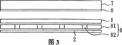
图3显示习知的嵌入式背光模组,其由下至上依序配置有:反射片2、含数个光源82的平面光板8及扩散片1,此模组与反射式偏光片6及液晶面板7结合即形成LCD。于此背光模组中,光源82可为直条状或点状配置的发光二极管(LED)或其它形状的光源,其安置于支撑体81中,支撑体81可为玻璃或压克力板。光线由光源82射出,直接射入扩散片1,藉由其中的扩散粒子产生折射、散射作用,以将光线均匀扩散;因为这种发光方式属于直接出光,正面辉度将大为提高;最后,在光线进入液晶面板7的前,进一步利用反射式偏光片6以提高正面以及大视角的亮度。设置在最下方的反射片2则藉由将经扩散片1反射至底部的光线再度反射回扩散片1,而得以增进对光源的使用效率。Figure 3 shows a known embedded backlight module, which is configured from bottom to top: a
然而,在依照上述配置的直下式与嵌入式背光模组中,液晶面板7在正对于光源3、82的正上方处会因为光源3、82的直接出光而有较高的辉度,而液晶面板7在位于于各光源3、82的间的上方处的辉度则较暗。此种因光源配置而造成的辉度不同、进而使液晶面板7上有明暗带的情况是显示于图2。However, in the direct type and embedded backlight modules according to the above configuration, the
目前对此问题的解决方式主要有二种:以图1为例,一为拉长光源3与导光板4、甚或扩散片1的间的距离,以降低此种明暗带现象;然而,一旦光源3与其它组件距离拉远后,除辉度即随的衰减外,背光模组的整体厚度亦随的增加,而这两种衍生的问题均违反对背光模组轻、薄、光利用率高的要求。At present, there are mainly two ways to solve this problem: Take Figure 1 as an example, one is to lengthen the distance between the
另一种方式则是在导光板4上设计凹槽或其它各种纹路,或是舍弃导光板4,而直接在扩散片1加入密度分布不均的萤光物质,以期透过光的散射而减低上述的明暗带现象;但是这两种方法均因为制程的繁复而不易达成,即使技术上可行,其增加的成本也非常可观,无法于量产上施行。Another way is to design grooves or other various lines on the
因此,在直下式背光模组领域中,需要在不降低光学性能(如辉度、亮度等)、不增加模组厚度、且不会大幅增加成本的前提下,对上述明暗带问题找出一解决方法。本发明即满足此需求。Therefore, in the field of direct-lit backlight modules, it is necessary to find a solution to the above light and dark band problem without reducing the optical performance (such as luminance, brightness, etc.), without increasing the thickness of the module, and without greatly increasing the cost. Solution. The present invention satisfies this need.
【发明内容】【Content of invention】
本发明的一目的为提供一种用于背光模组的光散射膜片,具有反射、散射、扩散、集光、混光等效果,使得由直下式或嵌入式背光模组所射出的光线能均匀分散,不至于相对于光源设置位置而在液晶面板上形成明暗带,从而提高出光辉度。An object of the present invention is to provide a light-scattering film for a backlight module, which has the effects of reflection, scattering, diffusion, light collection, and light mixing, so that the light emitted by a direct-type or embedded backlight module can Evenly dispersed, so as not to form light and dark bands on the liquid crystal panel relative to the position of the light source, thereby improving the luminance of light.
本发明的另一目的为提供一种用于背光模组的光散射膜片的制法,上述光散射膜片具有反射、散射、扩散、集光、混光等效果,此制法可易于导入目前使用的制造流程中,具有优异的兼容性,不会导致制造成本上额外的负担。Another object of the present invention is to provide a method for making a light-scattering film used in a backlight module. The above-mentioned light-scattering film has effects such as reflection, scattering, diffusion, light collection, and light mixing. This method can be easily introduced into In the currently used manufacturing process, it has excellent compatibility and will not cause an additional burden on the manufacturing cost.
本发明的又一目的为提供一种使用上述具有反射、散射、扩散、集光、混光等效果的光散射膜片的背光模组及据此形成的显示装置,该背光模组因为采用上述光散射膜片,而得以在不增加模组体积与成本的情形下,具有良好的出光辉度与均匀度,从而使得据此形成的显示装置具较佳的显示效果。Another object of the present invention is to provide a backlight module using the above-mentioned light-scattering film with effects of reflection, scattering, diffusion, light collection, and light mixing, and a display device formed therefrom. The light-scattering film can have good luminance and uniformity without increasing the volume and cost of the module, so that the display device formed therefrom has better display effect.
依本发明的用于背光模组的光散射膜片,该背光模组设有至少一个光源,其特征在于:该光散射膜片包含有:According to the light-scattering film for a backlight module of the present invention, the backlight module is provided with at least one light source, and it is characterized in that: the light-scattering film includes:
一基材层,具有二相对面;a substrate layer having two opposite surfaces;
一扩散层,其是形成于该基材层的一面上;以及a diffusion layer formed on one side of the substrate layer; and
一抗静电防粘着层,其具有第一表面与第二表面,该第一表面是形成于该基材层的另一相对面上,第二表面具有至少一个光路径调整单元,该光路径调整单元的设置是相关于该至少一个光源的设置,An antistatic anti-adhesion layer, which has a first surface and a second surface, the first surface is formed on the other opposite surface of the substrate layer, the second surface has at least one light path adjustment unit, the light path adjustment the setting of the unit is related to the setting of the at least one light source,
藉此,该至少一个光源的光线直接进入该抗静电防粘着层或经由该至少一个光路径调整单元调整路径后再进入该抗静电防粘着层,之后再经由该基材层及扩散层向外射出。In this way, the light of the at least one light source directly enters the antistatic anti-adhesion layer or enters the antistatic anti-adhesion layer after being adjusted by the at least one light path adjustment unit, and then passes through the base material layer and the diffusion layer to the outside shoot out.
依本发明的一种前述用于直下式与嵌入式背光模组的光散射膜片的制法,其步骤包含有:提供一充作基材层的透明或半透明层;于该透明或半透明层的二相对面上分别形成一扩散层及一具有第一表面与第二表面的抗静电防粘着层,该抗静电防粘着层的第一表面是与该透明或半透明层接合;以及于该抗静电防粘着层的第二表面形成至少一个光路径调整单元。According to a method for preparing a light-scattering film for direct-type and embedded backlight modules according to the present invention, the steps include: providing a transparent or translucent layer as a substrate layer; A diffusion layer and an antistatic anti-adhesion layer having a first surface and a second surface are respectively formed on two opposite surfaces of the transparent layer, the first surface of the antistatic anti-adhesion layer is bonded to the transparent or translucent layer; and At least one light path adjustment unit is formed on the second surface of the antistatic anti-adhesion layer.
依本发明的又一态样,一种背光模组,其是使用前述光散射膜片。According to another aspect of the present invention, a backlight module uses the aforementioned light-scattering film.
依本发明的再一态样,一种显示装置,其设有使用前述光散射膜片的背光模组。According to yet another aspect of the present invention, a display device is provided with a backlight module using the aforementioned light-scattering film.
本发明的一种用于背光模组的光散射膜片,具有反射、散射、扩散、集光、混光等效果,使得由直下式或嵌入式背光模组所射出的光线能均匀分散,不至于相对于光源设置位置而在液晶面板上形成明暗带,从而提高出光辉度。A light-scattering film for a backlight module of the present invention has the effects of reflection, scattering, diffusion, light collection, and light mixing, so that the light emitted by the direct-type or embedded backlight module can be evenly dispersed without As for the light and dark bands are formed on the liquid crystal panel relative to the position of the light source, so as to improve the luminance of light.
本发明的用于背光模组的光散射膜片的制法,此制法可易于导入目前使用的制造流程中,具有优异的兼容性,不会导致制造成本上额外的负担。The manufacturing method of the light-scattering film used in the backlight module of the present invention can be easily introduced into the currently used manufacturing process, has excellent compatibility, and will not cause additional burden on the manufacturing cost.
本发明的使用上述具有反射、散射、扩散、集光、混光等效果的光散射膜片的背光模组及据此形成的显示装置,该背光模组因为采用上述光散射膜片,而得以在不增加模组体积与成本的情形下,具有良好的出光辉度与均匀度,从而使得据此形成的显示装置具较佳的显示效果。The backlight module of the present invention using the above-mentioned light-scattering film having the effects of reflection, scattering, diffusion, light collection, and light mixing and the display device formed therefrom, the backlight module can be obtained by using the above-mentioned light-scattering film Without increasing the volume and cost of the module, it has good luminance and uniformity, so that the display device formed therefrom has better display effect.
【附图说明】【Description of drawings】
于所有图式中使用同样的标号以标示相同或类似的特征。这些图式并未按照比例绘制,且其仅是供阐示目的之用。The same reference numbers are used throughout the drawings to identify the same or similar features. The drawings are not drawn to scale and are for illustration purposes only.
图1为习知的直下式背光模组的示意结构图。FIG. 1 is a schematic structural diagram of a conventional direct-lit backlight module.
图2为图1的光源相对位置与出光面亮度关是坐标图。FIG. 2 is a coordinate diagram of the relationship between the relative position of the light source and the brightness of the light-emitting surface in FIG. 1 .
图3为习知的嵌入式背光模组的示意结构图。FIG. 3 is a schematic structural diagram of a conventional embedded backlight module.
图4为根据本发明的一实施例的光散射膜片的示意结构图。FIG. 4 is a schematic structural diagram of a light-scattering film according to an embodiment of the present invention.
图5为根据本发明的一实施例的光散射膜片所设置的光路径调整单元的示意剖面图。5 is a schematic cross-sectional view of a light path adjusting unit provided with a light scattering film according to an embodiment of the present invention.
图6为使用根据本发明的一实施例的光散射膜片的直下式背光模组的示意结构图。FIG. 6 is a schematic structural diagram of a direct-lit backlight module using a light-scattering film according to an embodiment of the present invention.
图7为使用根据本发明的一实施例的光散射膜片的嵌入式背光模组的示意结构图。FIG. 7 is a schematic structural view of an embedded backlight module using a light-scattering film according to an embodiment of the present invention.
【具体实施方式】【Detailed ways】
本发明的用于直下式与嵌入式背光模组的光散射膜片主要包含一基材层、一扩散层及一抗静电防粘着层,该扩散层形成于该基材层的一面上,该抗静电防粘着层的一表面形成于该基材层的另一面上,该抗静电防粘着层的另一表面则具有至少一个光路径调整单元,其设置主要是对应于背光模组所使用的至少一个光源的设置。运作中,模组中的至少一个光源射出的光线,可直接进入抗静电防粘着层,或经由光路径调整单元将部分光线散射后再进入抗静电防粘着层,之后再经由基材层及扩散层射出,使得射出的光线能均匀分散。The light-scattering film for direct-type and embedded backlight modules of the present invention mainly includes a base material layer, a diffusion layer and an antistatic anti-adhesion layer, the diffusion layer is formed on one side of the base material layer, the One surface of the antistatic anti-adhesion layer is formed on the other surface of the substrate layer, and the other surface of the antistatic anti-adhesion layer has at least one light path adjustment unit, which is mainly arranged corresponding to the backlight module. Settings for at least one light source. During operation, the light emitted by at least one light source in the module can directly enter the antistatic anti-adhesion layer, or part of the light can be scattered by the light path adjustment unit and then enter the antistatic anti-adhesion layer, and then pass through the substrate layer and diffuse The layer is emitted, so that the emitted light can be evenly dispersed.
该基材层可由包含但不仅限于聚对苯二甲酸乙二酯(PET)的高分子薄膜材料形成;该扩散层可由包含但不仅限于聚苯甲基丙烯酸丁酯(PMBA)等高分子树脂材料形成,能产生细致的表面粗糙度而提供均匀的光扩散效果,并具有集光功能(即提高光学辉度);该抗静电防粘着层可由包含但不仅限于聚甲基丙烯酸甲酯(PMMA)等高分子树脂材料形成,能于模组组装过程中避免污物粘着;该光路径调整单元可为包含但不限于由抗紫外线油墨形成的印刷网点。The substrate layer can be formed by polymer film materials including but not limited to polyethylene terephthalate (PET); the diffusion layer can be made of polymer resin materials including but not limited to polyphenylmethacrylate (PMBA). Formed, can produce fine surface roughness to provide a uniform light diffusion effect, and has a light-collecting function (that is, to improve optical brightness); the antistatic anti-adhesion layer can be composed of polymethylmethacrylate (PMMA) It is formed of polymer resin materials such as polymer resin, which can prevent dirt from sticking during the module assembly process; the light path adjustment unit can include but not limited to printing dots formed by UV-resistant ink.
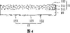
请参阅图4,其揭示本发明的一种用于背光模组的光散射膜片1’的一较佳实施例,该光散射膜片1’包含有一基材层10、一扩散层11与一抗静电防粘着层12,该扩散层11是形成于该基材层10的一面上,而该抗静电防粘着层12则形成于该基材层10的另一面上。该抗静电防粘着层12上表面与该基材层10接合,下表面则具有数个光路径调整单元123。Please refer to FIG. 4, which discloses a preferred embodiment of a light-scattering film 1' for a backlight module of the present invention. The light-scattering film 1' includes a
在此实施例中,基材层10的材料可为透明或半透明的树脂膜,其较佳为选自聚对苯二甲酸乙二酯(PET)、三乙酸纤维素(TAC)、聚萘甲酸乙二酯(PEN)、聚丙二酯、聚酰亚胺、聚醚、聚碳酸酯、聚胺、聚乙烯、聚丙烯或聚乙烯醇等等或其等效物。该树脂膜的厚度较佳为25至300微米(μm),更佳为50至200微米。In this embodiment, the material of the
扩散层11包含主要由有机透光散射粒子112与无机微小粒子113组成的数个扩散粒子,并包含粘着物111,将该数个扩散粒子固着至基材层10上。The
粘着物111的材料可为热可塑型高分子树脂,其较佳为选自(甲基)丙烯酸酯((meth)acrylate)的单独或聚合体、聚酯(polyester)、聚碳酸酯(polycarbonate)、聚苯乙烯(polystyrene)或聚甲基戊烯(polymethyl pentene)等等或其等效物。而其中该(甲基)丙烯酸酯的单独或聚合体较佳为选自聚(甲基)丙烯酸甲酯(polymethyl(meth)acrylate)或聚(甲基)丙烯酸乙酯(polyethyl(meth)acrylate)等,该聚酯较佳为聚乙烯对苯二甲酯(polyethylene terephthalate)或聚丙烯对苯二甲酯(polypropyrene terephthalates)等。粘着物111在该扩散层11内的重量百分比(weight%)的比例可为10重量百分比至90重量百分比,较佳为40重量百分比至80重量百分比。The material of the adhesive 111 can be a thermoplastic polymer resin, which is preferably selected from (meth)acrylate (meth)acrylate alone or polymer, polyester (polyester), polycarbonate (polycarbonate) , polystyrene (polystyrene) or polymethylpentene (polymethyl pentene), etc. or their equivalents. Wherein the (meth)acrylate alone or polymer is preferably selected from poly(meth)acrylate (polymethyl(meth)acrylate) or poly(meth)acrylate (polyethyl(meth)acrylate) etc., the polyester is preferably polyethylene terephthalate (polyethylene terephthalate) or polypropylene terephthalate (polypropylene terephthalates) and the like. The weight percent (weight%) of the adhesive 111 in the
有机透光散射粒子112较佳为选自聚甲基丙烯酸甲酯(PMMA)、聚苯甲基丙烯酸丁酯(polymethoxy benzyl acetate,PMBA)或聚氯乙烯(PVC)等等或其等效物。有机透光散射粒子112在扩散层11内的重量百分比的比例可为10重量百分比至90重量百分比,较佳为40重量百分比至80重量百分比。The organic light-transmitting scattering particles 112 are preferably selected from polymethyl methacrylate (PMMA), polymethoxy benzyl acetate (PMBA), polyvinyl chloride (PVC), etc. or their equivalents. The weight percent of the organic light-transmitting scattering particles 112 in the
无机微小粒子113较佳为选自SiO2、Al2O3或硅胶(silicon)等等或其等效物。无机微小粒子113在扩散层11内的重量百分比的比例可为30重量百分比至90重量百分比,较佳为40重量百分比至90重量百分比。The inorganic fine particles 113 are preferably selected from SiO2 , Al2 O3 , silica gel (silicon), etc. or their equivalents. The weight percent ratio of the inorganic fine particles 113 in the
在本实施例中,粘着物111可由聚(甲基)丙烯酸甲酯相对于扩散层11为10重量百分比至30重量百分比、聚乙烯对苯二甲酯相对于扩散层11为10重量百分比至30重量百分比所组成;有机透光散射粒子112可由PMMA相对于扩散层11为15重量百分比至40重量百分比、PMBA相对于扩散层11为10重量百分比至30重量百分比所组成;无机微小粒子113可由SiO2相对于扩散层11为10重量百分比至40重量百分比、硅胶相对于扩散层11为10重量百分比至30重量百分比所组成。扩散层11的厚度范围较佳为15至40微米。In this embodiment, the adhesive 111 can be made of poly(methyl)acrylate with a ratio of 10 weight percent to 30 weight percent relative to the
抗静电防粘着层12的结构与扩散层11基本上近似,其包含主要由有机透光散射粒子122组成的数个扩散粒子,并包含粘着物121,将该数个扩散粒子固着至基材层10上。不同处在于扩散粒子与粘着物的比例、抗静电防粘着层12的厚度以及在抗静电防粘着层12下表面上的光路径调整单元123,且抗静电防粘着层12是形成为使得其中的扩散粒子凸出于粘着物121的表面,从而抗静电防粘着层12与其它组件接触时,仅于凸出的扩散粒子处形成接触,其它部分则会形成间隙,故可达成抗静电防粘着目的。The structure of the
于抗静电防粘着层12中,粘着物121的重量百分比(weight%)的比例可为60重量百分比至95重量百分比,较佳为70重量百分比至90重量百分比,有机透光散射粒子122的重量百分比的比例可为5重量百分比至40重量百分比,较佳为10重量百分比至30重量百分比。In the
在本实施例中,粘着物121可由聚(甲基)丙烯酸甲酯相对于抗静电防粘着层12为10重量百分比至70重量百分比、聚乙烯对苯二甲酯相对于抗静电防粘着层12为10重量百分比至50重量百分比所组成;有机透光散射粒子122可由PMMA相对于抗静电防粘着层12为10重量百分比至30重量百分比所组成。抗静电防粘着层12的厚度范围较佳为10至25微米。In this embodiment, the adhesive 121 can be made of poly(meth)acrylate relative to the antistatic
光路径调整单元123主要是对应于背光模组的光源空间分布而设置在抗静电防粘着层12的下表面上。该空间分布乃为根据使用本光散射膜片1’的背光模组的光源配置而得,以直下式背光模组为例(参图1),可先将光源3以适当间隔排列于反射片2与导光板4的间后,再将光源3经由导光板4透射的影像以电荷耦合组件(Charge Coupled Device,CCD)或色度分光计(Chroma Spectrometer)高分辨率曝光摄相,从而得到有明暗区域的空间分布图,即辉度空间分布图,再以计算机软件(诸如PhotoShop等等)转换镜射图档,进而设计光路径调整单元123的配置图,之后可利用但不仅限于下列方式依此配置图将光路径调整单元123形成于抗静电防粘着层12的下表面上:The light
方式一:以抗紫外线油墨实施网点印刷(dot printing)来形成不透明或部分透明的光路径调整单元123,如图4所示;Mode 1: implement dot printing (dot printing) with UV-resistant ink to form an opaque or partially transparent light
方式二:以包含但不仅限于聚碳酸酯(PC)的半透明材料,经由涂布(coating)、真空蒸镀或离子溅镀等等加工方式,形成不同表面形状的光路径调整单元123,如图5所示,表面形状可为不规则V形的光路径调整单元1231,或不规则R形的光路径调整单元1232;Method 2: Use translucent materials including but not limited to polycarbonate (PC) to form optical
方式三:结合前述方式一及方式二来形成光路径调整单元123。Mode 3: Form the optical
可利用下列方法形成一种如前述实施例的光散射膜片1’。首先,将一充作该基材层10的透明基材装入一暂存箱中,以超音波震动并加热以清洁该基材层10,接着将其架于一涂布机台上,再将构成该扩散层11的配方装入该涂布机台中,激活机台将配方涂布于该透明基材的一面上;接着,将涂布完成后的半成品置放于恒温恒湿式烘箱中,以温度75℃至125℃进行干燥约1至15分钟,并于确认其厚度、特性符合所需之后,再对该基材层10的另一面重复前述步骤,亦即,将其架于涂布机台上,将构成该抗静电防粘着层12的配方装入该涂布机台中,将配方涂布于该透明基材的另一面上,所形成的该抗静电防粘着层12具有二表面,其上表面是与该透明基材相接,而其下表面则供之后设置光路径调整单元123之用;然后将此光散射膜片半成品置于恒温恒湿式烘箱内加以干燥并确认其厚度、特性符合所需。上述的涂布步骤亦可以静电喷涂取代。A light-scattering film 1' as in the foregoing embodiment can be formed by the following method. First, a transparent base material used as the
随后,以印刷方式将抗紫外线油墨依所欲配置图印制于此半成品的抗静电防粘着层12的下表面上,形成由多个印刷网点构成的光路径调整单元123。Subsequently, the anti-ultraviolet ink is printed on the lower surface of the antistatic and
最后,再将此光学膜片置于紫外线(UV)干燥机中,以温度250℃至500℃进行干燥。所得的成品即为如前述实施例的光散射膜片1’。Finally, the optical film is placed in an ultraviolet (UV) dryer and dried at a temperature of 250°C to 500°C. The resulting finished product is the light-scattering film 1' of the aforementioned embodiment.
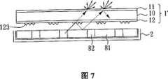
根据本发明所形成的光散射膜片1’可直接取代习知的扩散片(如图1的扩散片1)并用于各种习知显示装置的背光模组,例如图1、3所示的习知液晶显示装置的直下式与嵌入式背光模组,无须对该等背光模组进行额外的修正。一例示性的实施例如图6所示,其显示将本发明的光散射膜片1’直接应用于具有光源3的直下式背光模组中,于运作中,光源3射出的光线(如实线所示)可直接进入抗静电防粘着层12,或者光源3射出的光线(如虚线所示)可经由光路径调整单元123将部分光线散射/反射后再折射进入抗静电防粘着层12,之后再经由基材层10及扩散层11射出,使得射出的光线不但能均匀分散,且能提高出光辉度。另一例示性的实施例如图7所示,其显示将本发明的光散射膜片1’直接应用于具有光源82的嵌入式背光模组中,其运作方式类同于图6,其中另显示经由光路径调整单元123散射/反射的部分光线可于支撑体81表面散射/反射后再进入抗静电防粘着层12。The light-scattering film 1' formed according to the present invention can directly replace the known diffusion sheet (such as the
经实际测试显示,使用本发明的光散射膜片的显示装置的背光模组,可在不增加厚度、制程复杂度或成本的情形下,达到射出光线亮度均匀化并显著提高出光辉度的目的。The actual test shows that the backlight module of the display device using the light-scattering film of the present invention can achieve the purpose of uniforming the brightness of the emitted light and significantly improving the brightness of the emitted light without increasing the thickness, process complexity or cost. .
本发明已参照例示性实施例作详细说明,然而本说明并不意欲以限制性方式阐示。熟悉此项技艺人士在参照说明后,应可清楚理解例示性实施例的各种修正及结合、以及本发明的其它实施例。因此,任何此等修正或实施例均应属于本发明的保护范围。The present invention has been described in detail with reference to exemplary embodiments, however, this description is not intended to be construed in a restrictive manner. Various modifications and combinations of the exemplary embodiments, as well as other embodiments of the invention, will be apparent to those skilled in the art upon reference to the description. Therefore, any such amendments or embodiments shall belong to the protection scope of the present invention.
【组件符号说明】【Description of component symbols】
1:扩散片1: Diffuser
1’:光散射膜片1': Light-scattering film
2:反射片2: reflector
3:光源3: light source
4:导光板4: Light guide plate
5:增光片5: Enhancement film
6:反射式偏光片6: reflective polarizer
7:液晶面板7: LCD panel
8:平面光板8: flat light board
10:基材层10: Substrate layer
11:扩散层11: Diffusion layer
12:抗静电防粘着层12: Antistatic anti-adhesion layer
81:支撑体81: Support body
82:光源82: light source
111:粘着物111: Stickies
112:有机透光散射粒子112: Organic light-transmitting scattering particles
113:无机微小粒子113: Inorganic tiny particles
121:粘着物121: Stickies
122:有机透光散射粒子122: Organic light-transmitting scattering particles
123:光路径调整单元123: Optical path adjustment unit
1231:V形光路径调整单元1231: V-shaped light path adjustment unit
1232:R形光路径调整单元1232: R-shaped optical path adjustment unit
Claims (70)
Translated fromChinesePriority Applications (1)
| Application Number | Priority Date | Filing Date | Title |
|---|---|---|---|
| CN 200610067658CN101042488A (en) | 2006-03-24 | 2006-03-24 | Light-scattering film, its manufacturing method, and backlight module and display device using the same |
Applications Claiming Priority (1)
| Application Number | Priority Date | Filing Date | Title |
|---|---|---|---|
| CN 200610067658CN101042488A (en) | 2006-03-24 | 2006-03-24 | Light-scattering film, its manufacturing method, and backlight module and display device using the same |
Publications (1)
| Publication Number | Publication Date |
|---|---|
| CN101042488Atrue CN101042488A (en) | 2007-09-26 |
Family
ID=38808114
Family Applications (1)
| Application Number | Title | Priority Date | Filing Date |
|---|---|---|---|
| CN 200610067658PendingCN101042488A (en) | 2006-03-24 | 2006-03-24 | Light-scattering film, its manufacturing method, and backlight module and display device using the same |
Country Status (1)
| Country | Link |
|---|---|
| CN (1) | CN101042488A (en) |
Cited By (13)
| Publication number | Priority date | Publication date | Assignee | Title |
|---|---|---|---|---|
| CN101957465A (en)* | 2010-10-15 | 2011-01-26 | 中国乐凯胶片集团公司 | Optical diffusion film and preparation method thereof |
| CN102494253A (en)* | 2011-12-16 | 2012-06-13 | 苏州茂立光电科技有限公司 | Light source module |
| CN103375741A (en)* | 2012-04-30 | 2013-10-30 | 中强光电股份有限公司 | Light guide plate and backlight module using same |
| WO2014029145A1 (en)* | 2012-08-24 | 2014-02-27 | 深圳市华星光电技术有限公司 | Light guide plate and manufacturing method thereof |
| WO2014190676A1 (en)* | 2013-05-30 | 2014-12-04 | 京东方科技集团股份有限公司 | Exposure device and exposure method |
| US9008472B2 (en) | 2012-08-24 | 2015-04-14 | Shenzhen China Star Optoelectronics Technology Co., Ltd | Light guide plate and manufacturing method thereof |
| CN104865623A (en)* | 2015-06-17 | 2015-08-26 | 东莞市颖锋光电材料有限公司 | Three-in-one optical diffusion plate |
| CN105223729A (en)* | 2015-11-03 | 2016-01-06 | 昆山龙腾光电有限公司 | A kind of liquid crystal indicator |
| CN107474437A (en)* | 2017-09-01 | 2017-12-15 | 苏州罗格特光电科技有限公司 | A kind of preparation method of wide low temperature polyimide film material |
| CN107490902A (en)* | 2017-10-12 | 2017-12-19 | 京东方科技集团股份有限公司 | A kind of backlight module, display panel, display device |
| WO2018133361A1 (en)* | 2017-01-17 | 2018-07-26 | 京东方科技集团股份有限公司 | Backlight module and liquid crystal display device |
| CN111531998A (en)* | 2020-04-30 | 2020-08-14 | 王洛 | Optical polyester film |
| CN113682020A (en)* | 2021-09-03 | 2021-11-23 | 宁波东旭成新材料科技有限公司 | Antistatic reflective film of Mini-LED backlight module |
- 2006
- 2006-03-24CNCN 200610067658patent/CN101042488A/enactivePending
Cited By (16)
| Publication number | Priority date | Publication date | Assignee | Title |
|---|---|---|---|---|
| CN101957465A (en)* | 2010-10-15 | 2011-01-26 | 中国乐凯胶片集团公司 | Optical diffusion film and preparation method thereof |
| CN102494253A (en)* | 2011-12-16 | 2012-06-13 | 苏州茂立光电科技有限公司 | Light source module |
| US9329328B2 (en) | 2012-04-30 | 2016-05-03 | Coretronic Corporation | Light guide plate and backlight module using the same |
| CN103375741A (en)* | 2012-04-30 | 2013-10-30 | 中强光电股份有限公司 | Light guide plate and backlight module using same |
| WO2014029145A1 (en)* | 2012-08-24 | 2014-02-27 | 深圳市华星光电技术有限公司 | Light guide plate and manufacturing method thereof |
| US9008472B2 (en) | 2012-08-24 | 2015-04-14 | Shenzhen China Star Optoelectronics Technology Co., Ltd | Light guide plate and manufacturing method thereof |
| WO2014190676A1 (en)* | 2013-05-30 | 2014-12-04 | 京东方科技集团股份有限公司 | Exposure device and exposure method |
| US9500955B2 (en) | 2013-05-30 | 2016-11-22 | Boe Technology Group Co., Ltd. | Exposure apparatus and exposure method |
| CN104865623A (en)* | 2015-06-17 | 2015-08-26 | 东莞市颖锋光电材料有限公司 | Three-in-one optical diffusion plate |
| CN105223729A (en)* | 2015-11-03 | 2016-01-06 | 昆山龙腾光电有限公司 | A kind of liquid crystal indicator |
| WO2018133361A1 (en)* | 2017-01-17 | 2018-07-26 | 京东方科技集团股份有限公司 | Backlight module and liquid crystal display device |
| US10591773B2 (en) | 2017-01-17 | 2020-03-17 | Boe Technology Group Co., Ltd. | Backlight module and liquid crystal display device |
| CN107474437A (en)* | 2017-09-01 | 2017-12-15 | 苏州罗格特光电科技有限公司 | A kind of preparation method of wide low temperature polyimide film material |
| CN107490902A (en)* | 2017-10-12 | 2017-12-19 | 京东方科技集团股份有限公司 | A kind of backlight module, display panel, display device |
| CN111531998A (en)* | 2020-04-30 | 2020-08-14 | 王洛 | Optical polyester film |
| CN113682020A (en)* | 2021-09-03 | 2021-11-23 | 宁波东旭成新材料科技有限公司 | Antistatic reflective film of Mini-LED backlight module |
Similar Documents
| Publication | Publication Date | Title |
|---|---|---|
| CN101042488A (en) | Light-scattering film, its manufacturing method, and backlight module and display device using the same | |
| JP5824525B2 (en) | Light diffusion film and liquid crystal display backlight using the same | |
| CN1900744A (en) | Optical sheet, backlight assembly and display device | |
| CN1896837A (en) | Backlight module without light guide plate and diffuser plate | |
| CN1900775A (en) | Backlight unit and liquid crystal display comprising the same | |
| CN101571264B (en) | LED backlight module | |
| CN110727145A (en) | Backlight source and manufacturing method, backlight module, display panel, display device | |
| CN1940603A (en) | Optical member, method of manufacturing the optical member, and display device having the optical member | |
| CN1912716A (en) | Backlight unit and liquid crystal display having the same | |
| CN1928667A (en) | Backlight unit and display device having the same | |
| CN101118337A (en) | Optical plate and preparation method thereof, and backlight module using the optical plate | |
| CN102913825B (en) | Illumination unit, backlight module and display device | |
| CN1740864A (en) | Prism sheet for liquid crystal display and backlight unit using same | |
| CN105739009A (en) | Light guide plate and backlight module as well as manufacture method thereof and display device with same | |
| CN1847890A (en) | Light guide plate, backlight assembly, display device, and manufacturing method of light guide plate | |
| CN105068314A (en) | A direct type backlight module | |
| JP2007241272A (en) | Light diffusion film | |
| CN101354455A (en) | Diffusion brightening membrane | |
| WO2023155527A1 (en) | Backlight module and display apparatus | |
| CN111045253B (en) | Backlight module and liquid crystal display device | |
| CN1265277C (en) | Backlight module for thin film transistor liquid crystal display | |
| CN102967896A (en) | Light guide plate, backlight module and display device | |
| CN1637522A (en) | Back light structure of liquid crystal display device | |
| CN114895493A (en) | Backlight module and display device | |
| CN1743914A (en) | Be provided with the backlight assembly that improves light guide plate, and display device |
Legal Events
| Date | Code | Title | Description |
|---|---|---|---|
| C06 | Publication | ||
| PB01 | Publication | ||
| C10 | Entry into substantive examination | ||
| SE01 | Entry into force of request for substantive examination | ||
| C02 | Deemed withdrawal of patent application after publication (patent law 2001) | ||
| WD01 | Invention patent application deemed withdrawn after publication |