CN101038385A - Liquid crystal display panel and liquid crystal display panel having the same - Google Patents
Liquid crystal display panel and liquid crystal display panel having the sameDownload PDFInfo
- Publication number
- CN101038385A CN101038385ACNA2007101035794ACN200710103579ACN101038385ACN 101038385 ACN101038385 ACN 101038385ACN A2007101035794 ACNA2007101035794 ACN A2007101035794ACN 200710103579 ACN200710103579 ACN 200710103579ACN 101038385 ACN101038385 ACN 101038385A
- Authority
- CN
- China
- Prior art keywords
- display panel
- electrode
- electrically connected
- signal
- array base
- Prior art date
- Legal status (The legal status is an assumption and is not a legal conclusion. Google has not performed a legal analysis and makes no representation as to the accuracy of the status listed.)
- Pending
Links
Images


Classifications
- G—PHYSICS
- G02—OPTICS
- G02F—OPTICAL DEVICES OR ARRANGEMENTS FOR THE CONTROL OF LIGHT BY MODIFICATION OF THE OPTICAL PROPERTIES OF THE MEDIA OF THE ELEMENTS INVOLVED THEREIN; NON-LINEAR OPTICS; FREQUENCY-CHANGING OF LIGHT; OPTICAL LOGIC ELEMENTS; OPTICAL ANALOGUE/DIGITAL CONVERTERS
- G02F1/00—Devices or arrangements for the control of the intensity, colour, phase, polarisation or direction of light arriving from an independent light source, e.g. switching, gating or modulating; Non-linear optics
- G02F1/01—Devices or arrangements for the control of the intensity, colour, phase, polarisation or direction of light arriving from an independent light source, e.g. switching, gating or modulating; Non-linear optics for the control of the intensity, phase, polarisation or colour
- G02F1/13—Devices or arrangements for the control of the intensity, colour, phase, polarisation or direction of light arriving from an independent light source, e.g. switching, gating or modulating; Non-linear optics for the control of the intensity, phase, polarisation or colour based on liquid crystals, e.g. single liquid crystal display cells
- G02F1/133—Constructional arrangements; Operation of liquid crystal cells; Circuit arrangements
- G02F1/1333—Constructional arrangements; Manufacturing methods
- G02F1/13338—Input devices, e.g. touch panels
- B—PERFORMING OPERATIONS; TRANSPORTING
- B65—CONVEYING; PACKING; STORING; HANDLING THIN OR FILAMENTARY MATERIAL
- B65F—GATHERING OR REMOVAL OF DOMESTIC OR LIKE REFUSE
- B65F1/00—Refuse receptacles; Accessories therefor
- B65F1/14—Other constructional features; Accessories
- B65F1/141—Supports, racks, stands, posts or the like for holding refuse receptacles
- B65F1/1415—Supports, racks, stands, posts or the like for holding refuse receptacles for flexible receptables, e.g. bags, sacks
- A—HUMAN NECESSITIES
- A47—FURNITURE; DOMESTIC ARTICLES OR APPLIANCES; COFFEE MILLS; SPICE MILLS; SUCTION CLEANERS IN GENERAL
- A47B—TABLES; DESKS; OFFICE FURNITURE; CABINETS; DRAWERS; GENERAL DETAILS OF FURNITURE
- A47B81/00—Cabinets or racks specially adapted for other particular purposes, e.g. for storing guns or skis
- B—PERFORMING OPERATIONS; TRANSPORTING
- B65—CONVEYING; PACKING; STORING; HANDLING THIN OR FILAMENTARY MATERIAL
- B65B—MACHINES, APPARATUS OR DEVICES FOR, OR METHODS OF, PACKAGING ARTICLES OR MATERIALS; UNPACKING
- B65B67/00—Apparatus or devices facilitating manual packaging operations; Sack holders
- B65B67/12—Sack holders, i.e. stands or frames with means for supporting sacks in the open condition to facilitate filling with articles or materials
- B65B67/1222—Sack holders, i.e. stands or frames with means for supporting sacks in the open condition to facilitate filling with articles or materials characterised by means for suspending sacks, e.g. pedal- operated
- B65B67/1233—Clamping or holding means
- B—PERFORMING OPERATIONS; TRANSPORTING
- B65—CONVEYING; PACKING; STORING; HANDLING THIN OR FILAMENTARY MATERIAL
- B65F—GATHERING OR REMOVAL OF DOMESTIC OR LIKE REFUSE
- B65F1/00—Refuse receptacles; Accessories therefor
- B65F1/0033—Refuse receptacles; Accessories therefor specially adapted for segregated refuse collecting, e.g. receptacles with several compartments; Combination of receptacles
- B65F1/0053—Combination of several receptacles
- B65F1/0073—Flexible receptacles fixed on a frame or in an enclosure
- B—PERFORMING OPERATIONS; TRANSPORTING
- B65—CONVEYING; PACKING; STORING; HANDLING THIN OR FILAMENTARY MATERIAL
- B65F—GATHERING OR REMOVAL OF DOMESTIC OR LIKE REFUSE
- B65F1/00—Refuse receptacles; Accessories therefor
- B65F1/14—Other constructional features; Accessories
- B65F1/1468—Means for facilitating the transport of the receptacle, e.g. wheels, rolls
- B65F1/1473—Receptacles having wheels
- G—PHYSICS
- G06—COMPUTING OR CALCULATING; COUNTING
- G06F—ELECTRIC DIGITAL DATA PROCESSING
- G06F3/00—Input arrangements for transferring data to be processed into a form capable of being handled by the computer; Output arrangements for transferring data from processing unit to output unit, e.g. interface arrangements
- G06F3/01—Input arrangements or combined input and output arrangements for interaction between user and computer
- G06F3/03—Arrangements for converting the position or the displacement of a member into a coded form
- G06F3/041—Digitisers, e.g. for touch screens or touch pads, characterised by the transducing means
- G06F3/047—Digitisers, e.g. for touch screens or touch pads, characterised by the transducing means using sets of wires, e.g. crossed wires
- G—PHYSICS
- G09—EDUCATION; CRYPTOGRAPHY; DISPLAY; ADVERTISING; SEALS
- G09G—ARRANGEMENTS OR CIRCUITS FOR CONTROL OF INDICATING DEVICES USING STATIC MEANS TO PRESENT VARIABLE INFORMATION
- G09G3/00—Control arrangements or circuits, of interest only in connection with visual indicators other than cathode-ray tubes
- G09G3/20—Control arrangements or circuits, of interest only in connection with visual indicators other than cathode-ray tubes for presentation of an assembly of a number of characters, e.g. a page, by composing the assembly by combination of individual elements arranged in a matrix no fixed position being assigned to or needed to be assigned to the individual characters or partial characters
- G09G3/34—Control arrangements or circuits, of interest only in connection with visual indicators other than cathode-ray tubes for presentation of an assembly of a number of characters, e.g. a page, by composing the assembly by combination of individual elements arranged in a matrix no fixed position being assigned to or needed to be assigned to the individual characters or partial characters by control of light from an independent source
- G09G3/36—Control arrangements or circuits, of interest only in connection with visual indicators other than cathode-ray tubes for presentation of an assembly of a number of characters, e.g. a page, by composing the assembly by combination of individual elements arranged in a matrix no fixed position being assigned to or needed to be assigned to the individual characters or partial characters by control of light from an independent source using liquid crystals
- G09G3/3611—Control of matrices with row and column drivers
- G09G3/3648—Control of matrices with row and column drivers using an active matrix
- B—PERFORMING OPERATIONS; TRANSPORTING
- B65—CONVEYING; PACKING; STORING; HANDLING THIN OR FILAMENTARY MATERIAL
- B65B—MACHINES, APPARATUS OR DEVICES FOR, OR METHODS OF, PACKAGING ARTICLES OR MATERIALS; UNPACKING
- B65B67/00—Apparatus or devices facilitating manual packaging operations; Sack holders
- B65B67/12—Sack holders, i.e. stands or frames with means for supporting sacks in the open condition to facilitate filling with articles or materials
- B65B2067/1294—Holders for multiple sacks
- G—PHYSICS
- G02—OPTICS
- G02F—OPTICAL DEVICES OR ARRANGEMENTS FOR THE CONTROL OF LIGHT BY MODIFICATION OF THE OPTICAL PROPERTIES OF THE MEDIA OF THE ELEMENTS INVOLVED THEREIN; NON-LINEAR OPTICS; FREQUENCY-CHANGING OF LIGHT; OPTICAL LOGIC ELEMENTS; OPTICAL ANALOGUE/DIGITAL CONVERTERS
- G02F1/00—Devices or arrangements for the control of the intensity, colour, phase, polarisation or direction of light arriving from an independent light source, e.g. switching, gating or modulating; Non-linear optics
- G02F1/01—Devices or arrangements for the control of the intensity, colour, phase, polarisation or direction of light arriving from an independent light source, e.g. switching, gating or modulating; Non-linear optics for the control of the intensity, phase, polarisation or colour
- G02F1/13—Devices or arrangements for the control of the intensity, colour, phase, polarisation or direction of light arriving from an independent light source, e.g. switching, gating or modulating; Non-linear optics for the control of the intensity, phase, polarisation or colour based on liquid crystals, e.g. single liquid crystal display cells
- G02F1/133—Constructional arrangements; Operation of liquid crystal cells; Circuit arrangements
- G02F1/1333—Constructional arrangements; Manufacturing methods
- G02F1/1339—Gaskets; Spacers; Sealing of cells
- G02F1/13394—Gaskets; Spacers; Sealing of cells spacers regularly patterned on the cell subtrate, e.g. walls, pillars
- G—PHYSICS
- G02—OPTICS
- G02F—OPTICAL DEVICES OR ARRANGEMENTS FOR THE CONTROL OF LIGHT BY MODIFICATION OF THE OPTICAL PROPERTIES OF THE MEDIA OF THE ELEMENTS INVOLVED THEREIN; NON-LINEAR OPTICS; FREQUENCY-CHANGING OF LIGHT; OPTICAL LOGIC ELEMENTS; OPTICAL ANALOGUE/DIGITAL CONVERTERS
- G02F1/00—Devices or arrangements for the control of the intensity, colour, phase, polarisation or direction of light arriving from an independent light source, e.g. switching, gating or modulating; Non-linear optics
- G02F1/01—Devices or arrangements for the control of the intensity, colour, phase, polarisation or direction of light arriving from an independent light source, e.g. switching, gating or modulating; Non-linear optics for the control of the intensity, phase, polarisation or colour
- G02F1/13—Devices or arrangements for the control of the intensity, colour, phase, polarisation or direction of light arriving from an independent light source, e.g. switching, gating or modulating; Non-linear optics for the control of the intensity, phase, polarisation or colour based on liquid crystals, e.g. single liquid crystal display cells
- G02F1/133—Constructional arrangements; Operation of liquid crystal cells; Circuit arrangements
- G02F1/1333—Constructional arrangements; Manufacturing methods
- G02F1/1343—Electrodes
- G02F1/134309—Electrodes characterised by their geometrical arrangement
- G02F1/134363—Electrodes characterised by their geometrical arrangement for applying an electric field parallel to the substrate, i.e. in-plane switching [IPS]
- G—PHYSICS
- G09—EDUCATION; CRYPTOGRAPHY; DISPLAY; ADVERTISING; SEALS
- G09G—ARRANGEMENTS OR CIRCUITS FOR CONTROL OF INDICATING DEVICES USING STATIC MEANS TO PRESENT VARIABLE INFORMATION
- G09G2300/00—Aspects of the constitution of display devices
- G09G2300/04—Structural and physical details of display devices
- G09G2300/0421—Structural details of the set of electrodes
- G09G2300/0426—Layout of electrodes and connections
- G—PHYSICS
- G09—EDUCATION; CRYPTOGRAPHY; DISPLAY; ADVERTISING; SEALS
- G09G—ARRANGEMENTS OR CIRCUITS FOR CONTROL OF INDICATING DEVICES USING STATIC MEANS TO PRESENT VARIABLE INFORMATION
- G09G2300/00—Aspects of the constitution of display devices
- G09G2300/04—Structural and physical details of display devices
- G09G2300/0439—Pixel structures
- G09G2300/0443—Pixel structures with several sub-pixels for the same colour in a pixel, not specifically used to display gradations
- G—PHYSICS
- G09—EDUCATION; CRYPTOGRAPHY; DISPLAY; ADVERTISING; SEALS
- G09G—ARRANGEMENTS OR CIRCUITS FOR CONTROL OF INDICATING DEVICES USING STATIC MEANS TO PRESENT VARIABLE INFORMATION
- G09G2300/00—Aspects of the constitution of display devices
- G09G2300/04—Structural and physical details of display devices
- G09G2300/0439—Pixel structures
- G09G2300/0465—Improved aperture ratio, e.g. by size reduction of the pixel circuit, e.g. for improving the pixel density or the maximum displayable luminance or brightness
Landscapes
- Engineering & Computer Science (AREA)
- Physics & Mathematics (AREA)
- General Physics & Mathematics (AREA)
- Theoretical Computer Science (AREA)
- General Engineering & Computer Science (AREA)
- Nonlinear Science (AREA)
- Crystallography & Structural Chemistry (AREA)
- Mechanical Engineering (AREA)
- Chemical & Material Sciences (AREA)
- Optics & Photonics (AREA)
- Human Computer Interaction (AREA)
- Mathematical Physics (AREA)
- Computer Hardware Design (AREA)
- Liquid Crystal (AREA)
- Devices For Indicating Variable Information By Combining Individual Elements (AREA)
Abstract
Translated fromChinese
Description
Translated fromChinese技术领域technical field
本发明涉及一种显示面板、一种具有该显示面板的显示设备及其方法。尤其是,本发明涉及一种能够进行触摸屏功能的显示面板、具有该显示面板的显示设备及其方法。The present invention relates to a display panel, a display device with the display panel and a method thereof. In particular, the present invention relates to a display panel capable of a touch screen function, a display device having the same, and a method thereof.
背景技术Background technique
通常来说,液晶显示(“LCD”)设备利用液晶的光学和电学特性来显示图像,该光学和电学特性例如是各向异性的折射率、各向异性的介电常数等。相对于如阴极射线管(“CRT”)、等离子显示器(“PDP”)等显示设备来说,LCD设备具有一些特性,如结构较轻、功耗较低、驱动电压较低等。In general, a liquid crystal display ("LCD") device displays images using optical and electrical properties of liquid crystals, such as anisotropic refractive index, anisotropic dielectric constant, and the like. Compared with display devices such as cathode ray tube ("CRT"), plasma display ("PDP"), etc., LCD devices have some characteristics, such as lighter structure, lower power consumption, lower driving voltage, and the like.
通常来说,LCD设备包括具有控制接口的输入部分和计算数据以输出控制信号的系统部分。通过输入部分将数据提供给系统部分,且系统部分输出基于该数据的控制信号以显示图像。In general, an LCD device includes an input part having a control interface and a system part which calculates data to output a control signal. Data is supplied to the system section through the input section, and the system section outputs a control signal based on the data to display an image.
近来,LCD设备还包括利用显示在该LCD设备屏幕上的图标来接收数据的触摸板,从而用户直接向LCD面板输入数据。该触摸板检测手指或触摸物接触摸屏幕的触摸位置,并将触摸位置转换成输入信号以向LCD设备提供输入信号。当一台计算机包括具有该触摸板的LCD设备时,如键盘、鼠标等额外的输入部分便是不必要的了。此外,在如包括具有该触摸板的LCD设备的便携电话这样的移动装置中,如手机键盘这样的额外的输入部分便是不必要的了。因此,该触摸板得到广泛地应用。Recently, the LCD device also includes a touch panel that receives data using icons displayed on the screen of the LCD device, so that a user directly inputs data to the LCD panel. The touch panel detects a touch position where a finger or a touch object touches the screen, and converts the touch position into an input signal to provide the input signal to the LCD device. When a computer includes an LCD device having the touch panel, additional input sections such as a keyboard, a mouse, etc. are unnecessary. Furthermore, in a mobile device such as a portable phone including an LCD device having the touch panel, an additional input section such as a cell phone keypad is unnecessary. Therefore, the touch panel is widely used.
当触摸板被安装在LCD设备上时,具有该触摸板的LCD设备的厚度和尺寸增加了。为了减小该LCD设备的厚度和尺寸,将触摸板和LCD设备整体形成。当如手指的物体触摸与LCD设备整体形成的触摸板时,与手指触摸点相邻的区域内的液晶分子取向发生变化。由此,该LCD设备的屏幕上出现波纹,且显示质量劣化了。When the touch panel is mounted on the LCD device, the thickness and size of the LCD device having the touch panel increase. In order to reduce the thickness and size of the LCD device, the touch panel is integrally formed with the LCD device. When an object such as a finger touches the touch panel integrally formed with the LCD device, the orientation of liquid crystal molecules in an area adjacent to the point touched by the finger changes. As a result, moiré occurs on the screen of the LCD device, and the display quality is degraded.
发明内容Contents of the invention
本发明提供了一种能够进行触摸屏功能的显示面板。The invention provides a display panel capable of performing a touch screen function.
本发明还提供了一种具有该显示面板的显示设备。The invention also provides a display device with the display panel.
本发明还提供了一种在触摸屏功能期间防止显示质量劣化的方法。The present invention also provides a method of preventing deterioration of display quality during a touch screen function.
在本发明的示范性实施例中,显示面板包括阵列基板和相对基板。阵列基板包括多条数据线、与数据线相交的多条栅线、基本平行于栅线的多条第一信号线、基本平行于数据线的多条第二信号线、以及由彼此相邻的栅线和彼此相邻的数据线界定的多个像素。每个像素包括像素电极和绝缘于像素电极的公共电极。相对基板与阵列基板相结合来容纳液晶层,且其包括多个连接部件。由于外部提供的压力,至少一个连接部件电连接第一信号线和第二信号线中至少之一。In an exemplary embodiment of the present invention, a display panel includes an array substrate and an opposite substrate. The array substrate includes a plurality of data lines, a plurality of gate lines intersecting with the data lines, a plurality of first signal lines substantially parallel to the gate lines, a plurality of second signal lines substantially parallel to the data lines, and adjacent to each other A plurality of pixels defined by gate lines and data lines adjacent to each other. Each pixel includes a pixel electrode and a common electrode insulated from the pixel electrode. The opposite substrate is combined with the array substrate to accommodate the liquid crystal layer, and includes a plurality of connecting parts. At least one connection part electrically connects at least one of the first signal line and the second signal line due to pressure provided from the outside.
第一信号线基本上可以由与栅线基本相同的层形成,而第二信号线基本上可以由与数据线基本相同的层形成。The first signal line may be formed substantially of the same layer as the gate line, and the second signal line may be formed of substantially the same layer as the data line.
显示面板还可以包括用于维持阵列基板和相对基板之间的间隙的间隙维持部件。该间隙维持部件可以是柱状间隔物。The display panel may further include a gap maintaining member for maintaining a gap between the array substrate and the opposite substrate. The gap maintaining member may be a columnar spacer.
每个连接部件均可包括从相对基板突出的突起部和覆盖该突起部的导电层。Each connection part may include a protrusion protruding from the opposite substrate and a conductive layer covering the protrusion.
阵列基板还可以包括多个第一感测电极和多个第二感测电极。每个第一感测电极都被设置在相应的一条第一信号线上且电连接相应的一条第一信号线。每个第二感测电极都被设置在相应的一条第二信号线上且电连接相应的一条第二信号线。第一和第二感测电极基本上可由与像素电极相同的层形成。第一和第二感测电极可由与每个像素的公共电极基本上相同的层形成。The array substrate may further include a plurality of first sensing electrodes and a plurality of second sensing electrodes. Each first sensing electrode is disposed on a corresponding first signal line and is electrically connected to a corresponding first signal line. Each second sensing electrode is disposed on a corresponding second signal line and is electrically connected to a corresponding second signal line. The first and second sensing electrodes may be substantially formed of the same layer as the pixel electrode. The first and second sensing electrodes may be formed of substantially the same layer as the common electrode of each pixel.
或者,阵列基板还可以包括多个第一感测电极、多个第二感测电极和多个第三感测电极。每个第一感测电极都被设置在相应的一条第一信号线上且电连接相应的一条第一信号线。每个第二感测电极都被设置在相应的一条第二信号线上且电连接相应的一条第二信号线。每个第三感测电极都与第一和第二感测电极隔开设置且与每个连接部件相重叠。该阵列基板还可以包括用于向公共电极施加预定电压的公共电压线,且每个第三感测电极均可电连接该公共电压线。Alternatively, the array substrate may further include a plurality of first sensing electrodes, a plurality of second sensing electrodes and a plurality of third sensing electrodes. Each first sensing electrode is disposed on a corresponding first signal line and is electrically connected to a corresponding first signal line. Each second sensing electrode is disposed on a corresponding second signal line and is electrically connected to a corresponding second signal line. Each third sensing electrode is spaced apart from the first and second sensing electrodes and overlaps each connecting part. The array substrate may further include a common voltage line for applying a predetermined voltage to the common electrodes, and each third sensing electrode may be electrically connected to the common voltage line.
显示面板还可以包括阵列基板和相对基板之间的液晶层,其中,当显示面板工作期间该液晶层中的液晶分子可以在阵列基板上水平取向,且外部提供的压力基本上不会改变液晶分子的取向。The display panel can also include a liquid crystal layer between the array substrate and the opposite substrate, wherein the liquid crystal molecules in the liquid crystal layer can be horizontally aligned on the array substrate during the operation of the display panel, and the pressure provided by the outside will not substantially change the liquid crystal molecules orientation.
在本发明的其他示范性实施例中,一种显示设备包括显示面板、触摸位置检测部分和位置确定部分。该显示面板包括阵列基板和相对基板。该阵列基板包括多条数据线、与数据线相交的多条栅线、基本平行于栅线的多条第一信号线、基本平行于数据线的多条第二信号线、以及由彼此相邻的栅线和彼此相邻的数据线界定的多个像素。每个像素均包括像素电极和绝缘于像素电极的公共电极。该相对基板与阵列基板相结合来容纳液晶层,且其包括多个连接部件。由于外部提供的压力,至少一个连接部件电连接第一信号线和第二信号线中至少之一。触摸位置检测部分检测电连接到连接部件的第一和第二信号线以输出检测信号。位置确定部分基于检测信号来确定外部提供的压力的位置坐标。In other exemplary embodiments of the present invention, a display device includes a display panel, a touch position detection section, and a position determination section. The display panel includes an array substrate and an opposite substrate. The array substrate includes a plurality of data lines, a plurality of gate lines intersecting with the data lines, a plurality of first signal lines substantially parallel to the gate lines, a plurality of second signal lines substantially parallel to the data lines, and a plurality of adjacent The gate lines and the data lines adjacent to each other define a plurality of pixels. Each pixel includes a pixel electrode and a common electrode insulated from the pixel electrode. The opposite substrate is combined with the array substrate to accommodate the liquid crystal layer, and includes a plurality of connecting parts. At least one connection part electrically connects at least one of the first signal line and the second signal line due to pressure provided from the outside. The touch position detection part detects the first and second signal lines electrically connected to the connection part to output a detection signal. The position determination section determines position coordinates of the externally supplied pressure based on the detection signal.
显示面板还可以包括用于维持阵列基板和相对基板之间的间隙的间隙维持部件。该间隙维持部件可以是柱状间隔物。The display panel may further include a gap maintaining member for maintaining a gap between the array substrate and the opposite substrate. The gap maintaining member may be a columnar spacer.
阵列基板还可以包括多个第一感测电极和多个第二感测电极。每个第一感测电极被设置在相应的一条第一信号线上且被电连接到相应的一条第一信号线上。每个第二感测电极被设置在相应的一条第二信号线上且被电连接到相应的一条第二信号线上。第一和第二感测电极可由与像素电极基本相同的层形成。The array substrate may further include a plurality of first sensing electrodes and a plurality of second sensing electrodes. Each first sensing electrode is disposed on a corresponding one of the first signal lines and is electrically connected to the corresponding one of the first signal lines. Each second sensing electrode is disposed on a corresponding one of the second signal lines and is electrically connected to the corresponding one of the second signal lines. The first and second sensing electrodes may be formed of substantially the same layer as the pixel electrodes.
或者,阵列基板还可以包括多个第一感测电极、多个第二感测电极和多个第三感测电极。每个第一感测电极被设置在相应的一条第一信号线上且被电连接到相应的一条第一信号线上。每个第二感测电极被设置在相应的一条第二信号线上且被电连接到相应的一条第二信号线上。每个第三感测电极都与第一和第二感测电极隔开设置且与每个连接部件相重叠。该阵列基板还可以包括用于向公共电极施加预定电压的公共电压线,且每个第三感测电极均可电连接该公共电压线。Alternatively, the array substrate may further include a plurality of first sensing electrodes, a plurality of second sensing electrodes and a plurality of third sensing electrodes. Each first sensing electrode is disposed on a corresponding one of the first signal lines and is electrically connected to the corresponding one of the first signal lines. Each second sensing electrode is disposed on a corresponding one of the second signal lines and is electrically connected to the corresponding one of the second signal lines. Each third sensing electrode is spaced apart from the first and second sensing electrodes and overlaps each connecting part. The array substrate may further include a common voltage line for applying a predetermined voltage to the common electrodes, and each third sensing electrode may be electrically connected to the common voltage line.
触摸位置检测部分可以包括用于控制向第一和第二信号线施加的初始驱动电压的电压控制部分。触摸位置检测部分还可以包括数据采样部分,用于当外部提供的压力使至少一个连接部件电连接第一信号线和第二信号线中至少之一时检测第一和第二信号线的电压变化以及输出检测信号。该数据采样部分可以包括运算放大器。The touch position detection part may include a voltage control part for controlling the initial driving voltage applied to the first and second signal lines. The touch position detection part may further include a data sampling part for detecting a voltage change of the first and second signal lines when at least one connection part is electrically connected to at least one of the first and second signal lines by externally supplied pressure and Output detection signal. The data sampling section may include an operational amplifier.
在本发明的其他示范性实施例中,一种在进行液晶显示器的触摸屏功能期间防止显示质量劣化的方法包括提供带有像素电极、公共电极、电连接第一信号线的第一感测电极和电连接第二信号线的第二感测电极的阵列基板,提供带有从其突出的导电连接部件的相对基板,在阵列基板和相对基板间设置液晶层,当液晶显示器工作期间该液晶层中的液晶分子在阵列基板上水平取向,以及将外部提供的压力施加到相对基板上,以通过阵列基板上的第一和第二感测电极将连接部件电连接到第一和第二信号线,其中外部提供的压力基本不会改变液晶分子的取向。In other exemplary embodiments of the present invention, a method for preventing display quality degradation during a touch screen function of a liquid crystal display includes providing a first sensing electrode with a pixel electrode, a common electrode, electrically connected to a first signal line, and An array substrate electrically connected to the second sensing electrode of the second signal line, providing an opposite substrate with a conductive connection member protruding therefrom, a liquid crystal layer is arranged between the array substrate and the opposite substrate, and the liquid crystal layer in the liquid crystal layer during operation of the liquid crystal display the liquid crystal molecules are aligned horizontally on the array substrate, and externally provided pressure is applied to the opposite substrate to electrically connect the connection part to the first and second signal lines through the first and second sensing electrodes on the array substrate, Wherein, the pressure provided by the outside will basically not change the orientation of the liquid crystal molecules.
由上所述,显示面板包括具有像素电极和公共电极的阵列基板。因此,当该显示面板工作时,液晶分子在列阵基板上水平取向。因此,当将外部提供的压力施加到显示面板上以进行触摸屏功能时,外部提供的压力基本不会改变设置在阵列基板上的液晶分子的取向,且显示质量可以得到改进。As mentioned above, the display panel includes an array substrate having pixel electrodes and common electrodes. Therefore, when the display panel is in operation, the liquid crystal molecules are aligned horizontally on the array substrate. Therefore, when externally provided pressure is applied to the display panel for a touch screen function, the externally provided pressure does not substantially change the orientation of liquid crystal molecules disposed on the array substrate, and display quality may be improved.
附图说明Description of drawings
结合附图,通过下文的具体描述本发明的上述和其它特性和优点将变得显而易见,其中:The foregoing and other features and advantages of the present invention will become apparent from the following detailed description, taken in conjunction with the accompanying drawings, in which:
图1是用于说明根据本发明示范性实施例的示范性显示设备的框图;1 is a block diagram for explaining an exemplary display device according to an exemplary embodiment of the present invention;
图2是用于说明根据本发明示范性实施例的示范性显示面板的平面图;2 is a plan view for explaining an exemplary display panel according to an exemplary embodiment of the present invention;
图3是用于说明根据本发明示范性实施例的示范性显示面板的透视图;3 is a perspective view for explaining an exemplary display panel according to an exemplary embodiment of the present invention;
图4是用于说明根据本发明示范性实施例的示范性显示面板的一部分的平面图;4 is a plan view for explaining a part of an exemplary display panel according to an exemplary embodiment of the present invention;
图5是沿着图4中所示的线I-I’的剖面图;Fig. 5 is a sectional view along line I-I' shown in Fig. 4;
图6是用于说明当将外部提供的压力施加给相对基板时图4中的示范性显示面板的剖面图;6 is a cross-sectional view for explaining the exemplary display panel in FIG. 4 when externally provided pressure is applied to an opposite substrate;
图7是用于说明根据本发明另一示范性实施例的示范性显示面板的一部分的平面图;7 is a plan view for explaining a part of an exemplary display panel according to another exemplary embodiment of the present invention;
图8是沿着图7中所示的线ll-ll’的剖面图;Fig. 8 is a sectional view along line 11-11' shown in Fig. 7;
图9是用于说明当将外部提供的压力施加给相对基板时图7中的示范性显示面板的剖面图;FIG. 9 is a cross-sectional view for explaining the exemplary display panel in FIG. 7 when externally applied pressure is applied to an opposing substrate;
图10是用于示出利用根据本发明的示范性实施例的示范性显示面板来检测触摸位置的示范性方法的流程图;10 is a flowchart for illustrating an exemplary method of detecting a touch position using an exemplary display panel according to an exemplary embodiment of the present invention;
图11是用于说明根据本发明的示范性实施例的示范性显示面板的示范性触摸位置检测部分的示范性电路图;11 is an exemplary circuit diagram for explaining an exemplary touch position detection part of an exemplary display panel according to an exemplary embodiment of the present invention;
图12是用于说明根据本发明的另一示范性实施例的示范性显示面板的示范性触摸位置检测部分的示范性电路图。FIG. 12 is an exemplary circuit diagram for explaining an exemplary touch position detection part of an exemplary display panel according to another exemplary embodiment of the present invention.
具体实施方式Detailed ways
此后将结合附图更全面地描述本发明,在这些附图中示出了本发明的实施例。本发明可以多种不同形式实现,而并不应解释为仅局限于这里所阐述的实施例。相反,提供这些实施例是为了使本公开更为全面和完整,并使本领域的技术人员更充分地了解本发明的范围。为了清晰起见,在图中,层和区域的尺寸被放大了。The invention will be described more fully hereinafter with reference to the accompanying drawings, in which embodiments of the invention are shown. This invention may be embodied in many different forms and should not be construed as limited to only the embodiments set forth herein. Rather, these embodiments are provided so that this disclosure will be thorough and complete, and will fully convey the scope of the invention to those skilled in the art. In the drawings, the dimensions of layers and regions are exaggerated for clarity.
可以理解,当元件或层被提到在另一元件或层“上”、“连接到”或“耦合到”另一元件或层时,它可以直接在另一元件或层上、直接连接到或耦合到另一元件或层上,或可能存在中间的元件或层。相反,当元件被提到“直接”在另一元件或层“上”,“直接连接到”或“直接耦合到”另一元件或层时,则不存在中间的元件或层。在整个说明书中同样的参考数字表示同样的元件。如这里所使用的,术语“和/或”涵盖了相关的列出的项目中的任意一项或多项的任意组合。It will be understood that when an element or layer is referred to as being "on," "connected to," or "coupled to" another element or layer, it can be directly on, directly connected to, or the other element or layer. or coupled to another element or layer, or intervening elements or layers may be present. In contrast, when an element is referred to as being "directly on," "directly connected to" or "directly coupled to" another element or layer, there are no intervening elements or layers present. Like reference numerals refer to like elements throughout the specification. As used herein, the term "and/or" covers any combination of any one or more of the associated listed items.
可以理解,尽管第一、第二、第三等这些术语可以在这里使用来描述各种元件、组件、区域、层和/或部分,但这些元件、组件、区域、层和/或部分不应仅限于这些术语。这些术语只是被用来区分元件、组件、区域、层和/或部分与另外的元件、组件、区域、层和/或部分。因此,只要不脱离本发明的教导,下面所讨论的第一部分、组件、区域、层和/或部分可以被称为第二元件、组件、区域、层和/或部分。It will be understood that although the terms first, second, third, etc. may be used herein to describe various elements, components, regions, layers and/or sections, these elements, components, regions, layers and/or sections should not limited to these terms. These terms are only used to distinguish an element, component, region, layer and/or section from another element, component, region, layer and/or section. Thus, a first element, component, region, layer and/or section discussed below could be termed a second element, component, region, layer and/or section without departing from the teachings of the present invention.
空间关系术语,如“在…下面”、“在…之下”、“低于”、“在…之上”、“高于”等,可以在这里使用以用于简化图中所图示的一个元件或特征与另外的元件(或多个元件)或特征(或多个特征)关系的描述。可以理解,这些空间关系术语用于涵盖使用或操作中除图中所示的方位之外的装置的所有不同方位。例如,如果图中的装置被翻转,则被描述为在其它元件或特征之“下”或在其它元件或特征“下面”的元件这时将位于其它元件或特征之“上”。因此,示范性术语“在…之下”涵盖了在…之上和在…之下两个意思。装置还可以有其它定位(旋转90度或处于其它方位上),并因此解释这里所使用的空间关系描述语。Spatially relative terms, such as "below," "beneath," "below," "above," "above," etc., may be used herein to simplify what is illustrated in the figures. A description of the relationship of an element or feature to another element (or elements) or feature (or features). It will be understood that these spatially relative terms are intended to encompass all different orientations of the device in use or operation in addition to the orientation depicted in the figures. For example, if the device in the figures is turned over, elements described as "below" or "beneath" other elements or features would then be oriented "above" the other elements or features. Thus, the exemplary term "below" encompasses both above and below. The device is also capable of other orientations (rotated 90 degrees or at other orientations) and the spatially relative terms used herein interpreted accordingly.
这里所用的专有名词仅用于描述特定的实施例而并非意图限定本发明。如这里所用的,单数形式“一”、“一个”和“该”也意图涵盖复数形式,除非上下文清楚指明是其它情况。还应该理解,当在说明书中使用术语“包含”、“包括”时,指明了所述特征、整体、步骤、操作、元件和/或部件的存在,但是不排除一个或多个其它特征、整体、步骤、操作、元件和/或部件的存在。The terminology used herein is only used to describe specific embodiments and is not intended to limit the present invention. As used herein, the singular forms "a", "an" and "the" are intended to cover the plural forms as well, unless the context clearly dictates otherwise. It should also be understood that when the terms "comprises" and "comprises" are used in the specification, the existence of said features, integers, steps, operations, elements and/or components is indicated, but one or more other features, integers, or components are not excluded. , steps, operations, elements and/or components exist.
这里参考剖面图描述本发明的实施例,这些剖面图是本发明理想化的实施例(和中间构造)的示意图。因而,由于制造工艺和/或公差而导致的图示的形状不同是可以想见的。因此,本发明的实施例不应解释为限于这里图示的区域的特定形状而应包括例如由于制造而产生的形状的偏差。例如,图示为矩形的注入区域在它的边缘具有倒圆或曲线特征和/或注入浓度梯度,而非从注入到非注入区域的二元变化。同样地,通过注入形成的埋入区域可能导致在埋入区域和进行注入的表面之间的区域中一定的注入。因此,图中所示的区域本身仅是示意性的,它们的形状并非用于图示装置的实际形状,并且并非用于限制本发明的范围。Embodiments of the invention are described herein with reference to cross-section illustrations that are schematic illustrations of idealized embodiments (and intermediate constructions) of the invention. Thus, variations in the shapes of the illustrations as a result of manufacturing processes and/or tolerances are conceivable. Thus, embodiments of the invention should not be construed as limited to the particular shapes of regions illustrated herein but are to include deviations in shapes that result, for example, from manufacturing. For example, an implanted region illustrated as a rectangle may have rounded or curved features and/or a gradient of implant concentration at its edges rather than a binary change from implanted to non-implanted region. Likewise, a buried region formed by implantation may result in a certain implantation in the region between the buried region and the surface where the implantation takes place. Thus, the regions shown in the figures are schematic in themselves and their shapes are not intended to illustrate the actual shape of the device and are not intended to limit the scope of the invention.
除非另外定义,这里所使用的所有术语(包括技术和科学术语)具有与本发明所属领域的普通技术人员所通常理解的含义相同的含义。还应该理解,比如在通用的辞典中所定义的那些的术语,应解释为具有与它们在相关领域的环境中的含义相一致的含义,而不应以过度理想化或过度正式的含义来解释,除非在本文中明确地定义。Unless otherwise defined, all terms (including technical and scientific terms) used herein have the same meaning as commonly understood by one of ordinary skill in the art to which this invention belongs. It should also be understood that terms, such as those defined in commonly used dictionaries, should be interpreted to have a meaning consistent with their meaning in the context of the relevant field, and not in an overly idealistic or overly formal meaning , unless explicitly defined in this text.
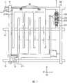
图1是用于说明根据本发明示范性实施例的示范性显示设备的框图。图2是用于说明根据本发明示范性实施例的示范性显示面板的平面图。图3是用于说明根据本发明示范性实施例的示范性显示面板的透视图;FIG. 1 is a block diagram for explaining an exemplary display device according to an exemplary embodiment of the present invention. FIG. 2 is a plan view for explaining an exemplary display panel according to an exemplary embodiment of the present invention. 3 is a perspective view for explaining an exemplary display panel according to an exemplary embodiment of the present invention;
参考图1和2,显示设备100包括显示面板200、面板驱动部分300、触摸位置检测部分400和位置确定部分500。Referring to FIGS. 1 and 2 , the
显示面板200包括阵列基板210、相对基板220和液晶层(未示出)。阵列基板210包括多个开关元件,如薄膜晶体管(TFT)。相对基板220面对阵列基板210。液晶层设置在阵列基板210和相对基板220之间。The
阵列基板210还可以包括多条沿阵列基板210的列方向即第二方向排列的数据线DL1、DL2、…DLm和多条沿阵列基板210的行方向即第一方向排列的栅线GL1、GL2、…GLn。The
阵列基板210的栅线GL1、GL2、…GLn的数量为n,且栅线GL1、GL2、…GLn沿第一方向D1延伸。阵列基板210的数据线DL1、DL2、…DLm的数量为m,且数据线DL1、DL2、…DL沿第二方向D2延伸。第二方向基本上垂直于第一方向D1。多个像素形成在由栅极GL1、GL2、…GLn和数据线DL1、DL2、…DLm限定的区域中。这里“n”和“m”是自然数。The number of gate lines GL1 , GL2 , . . . GLn of the
例如,TFT中的TFT211、公共电极(未示出)和像素电极(未示出)形成在其中第一数据线DL1和第一栅线GL1相交叉的区域中。TFT211的栅极电连接第一栅线GL1。TFT211的源极电连接第一数据线DL1。TFT211的漏极电连接像素电极。同样,m×n个TFT形成在数据线DL1、DL2、…DLm与栅线GL1、GL2、…GLn相交叉的区域内。For example, TFT211, a common electrode (not shown), and a pixel electrode (not shown) among the TFTs are formed in a region where the first data line DL1 and the first gate line GL1 cross. The gate of the TFT211 is electrically connected to the first gate line GL1. The source of the
参考图3,阵列基板210还可以包括多条第一信号线SL1和多条第二信号线SL2以进行触摸屏功能。第一信号线SL1沿第一方向D1延伸,而第二信号线SL2沿第二方向D2延伸。第一信号线SL1与第二信号线SL2相交叉,且与第二信号线SL2电绝缘。第一和第二信号线SL1和SL2电连接触摸位置检测部分400。Referring to FIG. 3 , the
第一和第二信号线SL1和SL2可以分别形成在单元像素部分中,而不是形成在每个像素中。每个单元像素部分均包括红(“R”)像素、绿(“G”)像素和蓝(“B”)像素。或者,第一和第二信号线SL1和SL2可以形成在多个单元像素部分中。例如,第一和第二信号线SL1和SL2可以分别形成在每四个单元像素部分中。The first and second signal lines SL1 and SL2 may be formed in unit pixel portions, respectively, instead of being formed in each pixel. Each unit pixel portion includes a red ("R") pixel, a green ("G") pixel, and a blue ("B") pixel. Alternatively, the first and second signal lines SL1 and SL2 may be formed in a plurality of unit pixel portions. For example, the first and second signal lines SL1 and SL2 may be formed in every four unit pixel portions, respectively.
相对基板220面对阵列基板210,且与阵列基板210相结合以在其间容纳液晶层。相对基板220可以是具有多个滤色片的滤色基板。或者,滤色片可以形成在阵列基板210上。The
此外,相对基板220还可以包括多个连接部件230以进行触摸屏功能。当外部提供的压力PO被施加到一个连接部件230上时,该连接部件230电连接形成在阵列基板210上的第一线号线SL1中的一条和第二信号线SL2中的一条。In addition, the
分别向第一和第二信号线SL1和SL2施加第一初始驱动电压Vid1和第二初始驱动电压Vid2。第一初始驱动电压Vid1与第二初始驱动电压Vid2的电平不同。当外部提供的压力PO被施加到一个连接部件230上时,该连接部件230电连接第一线号线SL1中的一条和第二信号线SL2中的一条。因此,施加到第一和第二信号线SL1和SL2每条上的电压电平被改变,由此检测外部提供的压力PO在显示面板200上的触摸位置。第一线号线SL1用来检测触摸位置的y-坐标,而第二信号线SL2用来检测触摸位置的x-坐标。The first initial driving voltage Vid1 and the second initial driving voltage Vid2 are applied to the first and second signal lines SL1 and SL2, respectively. The levels of the first initial driving voltage Vid1 and the second initial driving voltage Vid2 are different. When an externally provided pressure PO is applied to one
连接部件230可以分别形成在每个单元像素部分中。每个单元像素部分均包括红(“R”)像素、绿(“G”)像素和蓝(“B”)像素。或者,连接部件230可以形成在多个单元像素部分中。例如,连接部件230可以分别形成在每四个单元像素部分中。连接部件230可以与第一和第二信号线SL1和SL2相对应。The
面板驱动部分300包括定时控制部分310、电源部分320、灰度电压发生部分330、数据驱动部分340和栅驱动部分350。The
定时控制部分310控制显示设备100的运行。定时控制部分310基于RGB原始数据信号DATA_0和第一控制信号CNTL1产生第一数据信号DATA1、第二控制信号CNTL2、第三控制信号CNTL3和第四控制信号CNTL4。从如图像控制器的主系统向显示面板200提供RGB原始数据信号DATA_0和第一控制信号CNTL1。The
特别是,第一控制信号CNTL1包括主时钟信号MCLK、水平同步信号HSYNC和垂直同步信号VSYNC。第二控制信号CNTL2包括水平起始信号STH、反转信号REV和数据加载信号TP以用于控制数据驱动部分340。第三控制信号CNTL3包括起始信号STV、时钟信号CK和输出使能信号OE等,用于驱动栅驱动部分350。第四控制信号CNTL4包括另一时钟信号CLK和反转信号REV。In particular, the first control signal CNTL1 includes a main clock signal MCLK, a horizontal synchronization signal HSYNC, and a vertical synchronization signal VSYNC. The second control signal CNTL2 includes a horizontal start signal STH, an inversion signal REV, and a data loading signal TP for controlling the
定时控制部分310控制原始数据信号DATA_0的周期以向数据驱动部分320提供第一数据信号DATA1。The
定时控制部分310号可以输出第五控制信号CNTL5以控制触摸位置检测部分400。第五控制信号CNTL5包括另一时钟信号以控制从电源部分320输出的第一和第二初始驱动电压Vid1和Vid2,使得第一和第二初始驱动电压Vid1和Vid2被分别施加到第一和第二信号线SL1和SL2上。第一和第二初始驱动电压Vid1和Vid2可以为0V。The timing control part No. 310 may output a fifth control signal CNTL5 to control the touch
电源部分320产生施加到显示面板200上的公共电压Vcom和Vcst、施加给阵列基板210以进行触摸屏功能的第一和第二初始驱动电压Vid1和Vid2、施加给灰度电压发生部分330的模拟驱动电压AVDD、以及基于从定时控制部分310输出的第四控制信号CNTL4而施加到栅驱动部分350的栅开/关电压Von和Voff。The
灰度电压发生部分330使用从电源部分320输出的模拟驱动电压AVDD作为参考电压,基于具有对应于伽马曲线的电阻比率的区分电阻,产生了对应于灰度数量的多个参考灰度电压VGMA_R。The grayscale
如图2中所示,数据驱动部分340包括数据带载封装(“TCP”)341,数据TCP 341在其上承载了数据驱动芯片342。数据驱动部分340还可以包括多个TCP 341以将数据线DL1、DL2、…DLm划分为多个组。阵列基板210通过数据TCP 341电连接数据印刷电路板(“PCB”)360,定时控制部分310形成在该数据印刷电路板360上。As shown in FIG. 2, the
数据TCP 341基于来自定时控制部分310的第二控制信号CNTL2和由灰度电压发生部分330产生的灰度电压VGMA,将数字形式的第一数据信号DATA1改变为多个数据信号D1、D2、…Dm。数据TCP 341控制分别向数据线DL1、DL2、…DLm提供数据信号D1、D2、…Dm的输出定时。The data TCP 341 changes the first data signal DATA1 in digital form into a plurality of data signals D1, D2, . Dm. The data TCP 341 controls the output timing of providing data signals D1, D2, ... Dm to the data lines DL1, DL2, ... DLm, respectively.
栅驱动部分350包括用于其上承载栅驱动芯片的栅TCP 351。栅驱动部分350还可以包括多个栅TCP351以将栅线GL1、GL2、…GLn划分为多个组。栅TCP 351分别向栅线GL1、GL2、…GLn施加基于从定时控制部分310输出的第三控制信号CNTL3和由电源部分320输出的栅开/关电压Von和Voff的栅信号G1、G2、…Gn。The
触摸位置检测部分400检测施加到相对基板220上的外部提供的压力PO的触摸位置。The touch
当外部提供的压力PO施加到相对基板220时,连接部件230电连接第一线号线SL1中的一条和第二信号线SL2中的一条以改变被施加给第一线号线SL1的第一初始驱动电压Vid1的电平,由此检测外部提供的压力PO的y-坐标。When a pressure PO supplied from the outside is applied to the opposing
此外,当外部提供的压力PO施加到相对基板220时,连接部件230电连接第一线号线SL1和第二信号线SL2以改变被施加给第二线号线SL2的第二初始驱动电压Vid2的电平,由此检测外部提供的压力PO的x-坐标。In addition, when a pressure PO provided from the outside is applied to the
正如之后将参考图11和图12而进一步描述的,触摸位置检测部分400还可以包括电压控制部分和数据采样部分。电压控制部分基于第五控制信号CNTL5分别向第一和第二信号线SL1和SL2施加第一和第二初始驱动电压Vid1和Vid2。数据采样部分检测每条第一和第二信号线SL1和SL2的电压变化以输出第一和第二检测信号DS1和DS2。As will be further described later with reference to FIGS. 11 and 12 , the touch
触摸位置检测部分400可以形成在面板驱动部分300的数据驱动部分340上。具体而言,触摸位置检测部分400可以与数据驱动部分340的数据驱动芯片342整体形成。当触摸位置检测部分400与数据驱动芯片342整体形成时,该数据驱动芯片342还可以包括额外的电连接第一和第二信号线SL1和SL2的焊盘。如图3所示,尽管第一信号线SL1基本上沿第一方向D1延伸时,但是每条第一信号线SL1的端部可以被弯曲以沿第二方向D2延伸,从而连接第一信号线SL1与数据驱动芯片342中的额外的焊盘。The touch
位置确定部分500基于由触摸位置检测部分400输出的第一和第二检测信号DS1和DS2来处理y-坐标和x-坐标以确定被施加给显示面板200的外部提供的压力PO的位置。The
图4是用于说明根据本发明示范性实施例的示范性显示面板的一部分的平面图。图5是沿着图4中所示的线I-I’的剖面图。图6是用于说明当外部提供的压力被施加到相对基板上时图4的示范性显示面板的剖面图。FIG. 4 is a plan view for explaining a part of an exemplary display panel according to an exemplary embodiment of the present invention. Fig. 5 is a sectional view along line I-I' shown in Fig. 4 . FIG. 6 is a cross-sectional view for explaining the exemplary display panel of FIG. 4 when externally applied pressure is applied to the opposite substrate.
参考图3和4,阵列基板210包括多个以矩阵形状排列的像素。每个像素由彼此相邻的栅线GL和彼此相邻的数据线DL限定。每个像素包括公共电压线CL、TFT 211、公共电极212和像素电极214。至少一个像素还可以包括第一信号线SL1、第二信号线SL2、第一感测电极ES1和第二感测电极ES2。3 and 4, the
栅线GL沿第一方向D1延伸,而数据线DL沿基本上垂直于第一方向D1的第二方向D2延伸。栅线GL与数据线DL电绝缘。The gate lines GL extend in a first direction D1, and the data lines DL extend in a second direction D2 substantially perpendicular to the first direction D1. The gate line GL is electrically insulated from the data line DL.
第一线号线SL1沿第一方向D1延伸,而第二信号线SL2沿第二方向D2延伸。将第一初始驱动电压Vid1施加给第一信号线SL1,将第二初始驱动电压Vid2施加给第二信号线SL2。The first line number line SL1 extends along the first direction D1, and the second signal line SL2 extends along the second direction D2. The first initial driving voltage Vid1 is applied to the first signal line SL1, and the second initial driving voltage Vid2 is applied to the second signal line SL2.
第一感测电极ES1可以形成在第一信号线SL1上,而第二感测电极ES2可以形成在第二信号线SL2上。即,第一感测电极ES1电连接第一信号线SL1,而第二感测电极ES2电连接第二信号线SL2。当向相对基板220施加外部提供的压力PO时,第一和第二感测电极ES1和ES2与形成在相对基板220上的连接部件230相连。具体而言,第一信号线SL1通过第一感测电极ES1与连接部件230相连,第二信号线SL2通过第二感测电极ES2与连接部件230相连。第一和第二感测电极ES1和ES2通过过孔VH与第一和第二信号线SL1和SL2相连。The first sensing electrode ES1 may be formed on the first signal line SL1, and the second sensing electrode ES2 may be formed on the second signal line SL2. That is, the first sensing electrode ES1 is electrically connected to the first signal line SL1, and the second sensing electrode ES2 is electrically connected to the second signal line SL2. When an externally provided pressure PO is applied to the
像素电极214电连接TFT 211。像素电极214可以包括如氧化铟锡(“ITO”)和氧化铟锌(“IZO”)等的透明导电材料。像素电极214包括沿第一方向D1延伸的主像素电极214a和多个从主像素电极214a沿第二方向D2延伸的次像素电极214b。The
主像素电极214a与栅线GL相邻。主像素电极214a的一端电连接TFT211。通过主像素电极214a将信号电压施加给每个次像素电极214b。在所述的实施例中,次像素电极214b包括第一次像素电极、第二次像素电极、第三次像素电极和第四次像素电极,但是次像素电极214b的数量可以因需增加或减少。The
公共电压线CL沿第一方向延伸。公共电压线CL可以与栅线GL由阵列基板210基本相同的层形成。公共电极212可以与像素电极214由阵列基板210基本相同的层形成,且其可以通过过孔VH电连接公共电压线CL。通过公共电压线CL将公共电压施加给公共电极212。公共电压212可以包括如ITO和IZO等的透明导电材料。The common voltage line CL extends in the first direction. The common voltage line CL may be formed of substantially the same layer of the
公共电极212包括沿第一方向D1延伸的主公共电极212a和多个从主公共电极212a沿第二方向D2延伸的次公共电极212b。主公共电极212a平行于主像素电极214a延伸,而次公共电极212b平行于次像素电极214b延伸。在所述的实施例中,次公共电极212b包括第一次公共电极、第二次公共电极、第三次公共电极和第四次公共电极,但是次公共电极212b的数量可以因需增加或减少。次像素电极214b与次公共电极212b可以相互替换地排列在像素区域中。公共电极212和像素电极214间形成电场以控制设置在阵列基板210和相对基板220之间的液晶层的液晶分子的取向。The
公共电极212和像素电极214可为多种形状,如弯曲形、斜坡形等,使得公共电极212形成在其上形成了像素电极214的基板上。The
参考图4和5,显示面板200包括阵列基板210、相对基板220和间隙维持部件240。Referring to FIGS. 4 and 5 , the
TFT 211形成在阵列基板210的第一基底基板200a上。平坦化层213覆盖TFT 211与第一和第二信号线SL1和SL2。第一和第二感测电极ES1和ES2、像素电极214和公共电极212形成在平坦化层213上。The
TFT 211包括栅极211a、栅绝缘层211b、有源层211c、欧姆接触层211d、源极211e、漏极211f和保护层211g。The
栅极211a从栅线GL延伸。栅绝缘层211b覆盖栅极211a且保护栅极211a。栅绝缘层211b也覆盖栅线GL、第一信号线SL1、公共电压线CL和第一基底基板200a的任何外露部分。有源层211c和欧姆接触层211d相继形成在栅绝缘层211b上。欧姆接触层211d的一部分被除去以使有源层211c的一部分外露。源极211e和漏极211f形成在欧姆接触层211d上。源极211e从数据线DL延伸。漏极211f与数据线DL分离地形成。保护层211g形成在源极211e和漏极211f上,也形成在第二信号线SL2、数据线DL和栅绝缘层211b的任何外露部分上。保护层211g的一部分和平坦化层213的一部分被除去以使漏极211f的外一部分外露。The
第一信号线SL1由与栅线GL基本上相同的层形成,而第二信号线SL2由与栅线DL基本上相同的层形成。The first signal line SL1 is formed of substantially the same layer as the gate line GL, and the second signal line SL2 is formed of substantially the same layer as the gate line DL.
第一感测电极ES1形成在第一信号线SL1上。第一感测电极ES1形成在平坦化层213上,且通过贯穿平坦化层213、保护层211g和栅绝缘层211b的过孔VH电连接第一信号线SL1。当外部提供的压力PO被施加给相对基板220时,第一信号线SL1通过第一感测电极ES1与连接部件230电连接。第二感测电极ES2形成在第二信号线SL2上。第二感测电极ES2形成在平坦化层213上,且通过贯穿平坦化层213和保护层211g的过孔VH与连接部件230电连接。当外部提供的压力PO被施加给相对基板220时,第二信号线SL2通过第一感测电极ES2与连接部件230电连接。为了阻止像素开口率的减小,第一和第二感测电极ES1和ES2可以形成在非显示区域,例如在有光阻挡层形成的区域中。为了使第一和第二感测电极ES1和ES2彼此相邻设置,分叉部可以从第一信号线SL1和第二信号线SL2延伸。在所示的实施例中,来自第一信号线SL1的分叉部可以平行于第二信号线SL2延伸,而来自第二信号线SL2的分叉部可以平行于第一信号线SL1延伸。通过所述的分叉部来第一和第二感测电极ES1和ES2设置,可以有助于防止像素开口率减小,但是带有或不带有分叉部的第一和第二感测电极ES1和ES2的替换构造也在这些实施例的范围之内。每个第一和第二感测电极ES1和ES2均可包括如ITO和IZO等的透明导电材料。The first sensing electrode ES1 is formed on the first signal line SL1. The first sensing electrode ES1 is formed on the
第一信号线SL1设置在栅绝缘层211b、保护层211g和平坦化层213之下。第一信号线SL1通过过孔VH电连接第一感测电极ES1。第二信号线SL2被设置在保护层211g和平坦化层213之下。第二信号线SL2通过过孔VH电连接第二感测电极ES2。The first signal line SL1 is disposed under the
相对基板220包括第二基板200a和连接部件230。第二基板200a可以包括如玻璃、合成聚合物等的透明绝缘材料。例如,第二基板200a可以包括弹性相对较小的聚碳酸酯(“PC”)。或者,第二基板200a可以包括通过蚀刻工艺、研磨工艺等形成的玻璃板以具有相对较小的厚度。The
连接部件230从相对基板220突出预定的高度,且连接部件230的高度小于阵列基板210和相对基板220间的单元间隙。连接部件230的高度小于间隙维持部件240的高度。The
连接部件230具有突出部230a和导电层230b且与第一和第二感测电极ES1和ES2相交叠。突出部230a从相对基板220突出。例如,突出部230a可以在与间隙维持部件240相同的相对基板220的层形成。导电层230b覆盖突出部230a。导电层230b可以覆盖突出部230a距离阵列基板210最近的下端。导电层230b可包括如ITO和IZO等的透明导电材料。The
间隙维持部件240维持阵列基板210和相对基板220间的单元间隙。间隙维持部件240的实例包括柱状间隔物、球状间隔物等。球状间隔物的弹力大于柱状间隔物。The
参考图5和6,当向相对基板220施加外部提供的压力PO时,连接部件230与第二基板220a一起向阵列基板210运动以接触第一和第二感测电极ES1和ES2。因为连接部件230包括导电层230b,所以当连接部件230接触第一和第二感测电极ES1和ES2时,第一和第二感测电极ES1和ES2彼此电连接。第一和第二感测电极ES1和ES2通过过孔VH分别电连接第一和第二信号线SL1和SL2。因此,第一和第二信号线SL1和SL2彼此电连接。因此,施加到第一和第二信号线SL1和SL2每条上的电压电平变化了。5 and 6, when an externally provided pressure PO is applied to the
当施加到相对基板220上的外部提供的压力PO被去掉时,连接部件230通过第二基板220a的弹性和间隙维持部件240的弹性从阵列基板210沿相反方向运动。因此将连接部件230与第一和第二感测电极ES1和ES2隔开。When the externally provided pressure PO applied to the
图7是用于说明根据本发明另一示范性实施例的示范性显示面板的一部分的平面图。图8是沿着图7中所示的线ll-ll’的剖面图。图9是用于说明当将外部提供的压力PO施加给相对基板时图7中的示范性显示面板的剖面图。FIG. 7 is a plan view for explaining a part of an exemplary display panel according to another exemplary embodiment of the present invention. FIG. 8 is a cross-sectional view along line 11-11' shown in FIG. 7 . FIG. 9 is a cross-sectional view for explaining the exemplary display panel in FIG. 7 when an externally provided pressure PO is applied to an opposing substrate.
参考图3和7,显示面板201包括具有多个以矩阵形式排列的像素的阵列基板210。每个像素均由彼此相邻的栅线GL和彼此相邻的数据线DL限定。每个像素均包括公共电压线CL、TFT 211、公共电极212和像素电极214。TFT 211、公共电极212和像素电极214基本与图5中所示的TFT、公共电极和像素电极相同。至少一个像素还可以包括第一信号线SL1、第二信号线SL2、第一感测电极ES1、第二感测电极ES2和第三感测电极ES3。3 and 7, the
栅线GL沿第一方向D1延伸,而数据线DL沿大致垂直于第一方向D1的第二方向D2延伸。栅线GL与数据线DL电绝缘。公共电压线CL沿第一方向D1延伸且基本上可以由与栅线GL相同的层形成。The gate lines GL extend along a first direction D1, and the data lines DL extend along a second direction D2 substantially perpendicular to the first direction D1. The gate line GL is electrically insulated from the data line DL. The common voltage line CL extends in the first direction D1 and may be formed of substantially the same layer as the gate line GL.
第一线号线SL1沿第一方向D1延伸,而第二信号线SL2沿第二方向D2延伸。第一信号线SL1可以由与栅线GL基本上相同的层形成,而第二信号线SL2可以由与数据线DL基本上相同的层形成。第一和第二信号线SL1和SL2接地。因此,每条第一和第二信号线SL1和SL2均施加有0V的初始驱动电压。The first line number line SL1 extends along the first direction D1, and the second signal line SL2 extends along the second direction D2. The first signal line SL1 may be formed of substantially the same layer as the gate line GL, and the second signal line SL2 may be formed of substantially the same layer as the data line DL. The first and second signal lines SL1 and SL2 are grounded. Therefore, each of the first and second signal lines SL1 and SL2 is applied with an initial driving voltage of 0V.
第一感测电极ES1可以形成在第一信号线SL1上,而第二感测电极ES2可以形成在第二信号线SL2上。第三感测电极ES3形成在公共电压线CL上。为使第一、第二和第三感测电极ES1、ES2和ES3彼此相邻设置,分叉部可以从第一信号线SL、第二信号线SL2和公共电压线CL延伸出来。在所述的实施例中,来自公共电压线CL和第一信号线SL的分叉部彼此相对延伸且平行于第二信号线SL2,而来自第二信号线SL2的分叉部可平行于第一信号线SL1和公共电压线CL且在它们之间延伸。通过所述的分叉部来设置第一、第二和第三感测电极ES1、ES2和ES3可以有助于防止像素开口率的减小,但是带有或不带有分叉部的第一、第二和第三感测电极ES1、ES2和ES3的替换构造也在这些实施例的范围之内。当向相对基板220施加外部提供的压力PO时,第一到第三感测电极ES1到ES3与连接部件235接触。具体而言,连接部件235通过第一感测电极ES1电连接第一信号线SL1,连接部件235通过第二感测电极ES2电连接第二信号线SL2,且连接部件235通过第三感测电极ES3电连接公共电压线CL。第一到第三感测电极ES1到ES3通过过孔VH分别电连接第一信号线SL、第二信号线SL2和公共电压线CL。The first sensing electrode ES1 may be formed on the first signal line SL1, and the second sensing electrode ES2 may be formed on the second signal line SL2. The third sensing electrode ES3 is formed on the common voltage line CL. For the first, second, and third sensing electrodes ES1, ES2, and ES3 to be disposed adjacent to each other, bifurcated portions may extend from the first signal line SL, the second signal line SL2, and the common voltage line CL. In the described embodiment, the bifurcations from the common voltage line CL and the first signal line SL extend opposite to each other and parallel to the second signal line SL2, while the bifurcations from the second signal line SL2 may be parallel to the second signal line SL2. A signal line SL1 and a common voltage line CL extend between them. Arranging the first, second and third sensing electrodes ES1, ES2 and ES3 through the bifurcated part can help to prevent the reduction of the pixel aperture ratio, but the first sensor with or without the bifurcated part Alternative configurations of the second and third sense electrodes ES1, ES2 and ES3 are also within the scope of these embodiments. When an externally provided pressure PO is applied to the
参考图7和8,显示面板201包括阵列基板210、相对基板220和间隙维持部件240。Referring to FIGS. 7 and 8 , the
第一信号线SL1、第二信号线SL2和公共电压线CL形成在第一基底基板200a上。平坦化层213形成在第一信号线SL1、第二信号线SL2和公共电压线CL上。第一到第三感测电极ES1到ES3形成在平坦化层213上。The first signal line SL1, the second signal line SL2 and the common voltage line CL are formed on the
第一感测电极ES1形成在第一信号线SL1上。第二感测电极ES2形成在第二信号线SL2上。第三感测电极ES3形成在公共电压线CL上。为了防止像素开口率的减小,第一到第三感测电极ES1和ES2可以形成在非显示区域,例如在其中形成了光阻挡层的区域中。每个第一到第三感测电极ES1到ES3可以包括如ITO和IZO等的透明导电材料。The first sensing electrode ES1 is formed on the first signal line SL1. The second sensing electrode ES2 is formed on the second signal line SL2. The third sensing electrode ES3 is formed on the common voltage line CL. In order to prevent a decrease in pixel aperture ratio, the first to third sensing electrodes ES1 and ES2 may be formed in a non-display area, for example, an area in which a light blocking layer is formed. Each of the first to third sensing electrodes ES1 to ES3 may include a transparent conductive material such as ITO and IZO.
将第一信号线SL1设置在栅绝缘层211b、保护层211g和平坦化层213之下。第一信号线SL1通过过孔VH电连接第一感测电极ES1。将第二信号线SL2设置在保护层211g和平坦化层213之下。第二信号线SL2通过过孔VH电连接第二感测电极ES2。将公共电压线CL设置在栅绝缘层211b、保护层211g和平坦化层213之下。公共电压线CL通过过孔VH电连接第三感测电极ES3。The first signal line SL1 is disposed under the
连接部件235具有突出部235a和导电层235b,且与第一到第三感测电极ES1到ES3相重叠。即,当相对基板220和阵列基板210装配在一起且液晶层位于它们之间时,将连接部件235设置在相对基板220与第一到第三感测电极ES1到ES3相重叠的位置上。突出部235a从相对基板220突出。例如,突出部235a可以与间隙维持部件240一起形成。即,突出部235a可以与间隙维持部件240在基本上相同的制作步骤中形成。导电层235b覆盖突出部235a。导电层235b可以覆盖突出部235a的下端。导电层235b可以包括如ITO和IZO等的透明导电材料。The
参考图8和9,当向相对基板220施加外部提供的压力PO时,连接部件235和第二基板220a一起向阵列基板210移动以接触第一到第三感测电极ES1到ES3。第一到第三感测电极ES1到ES3通过过孔VH分别电连接第一信号线SL1、第二信号线SL2和公共电压线CL。因此,第一信号线SL1、第二信号线SL2和公共电压线CL彼此电连接。因此,施加到每条第一和第二信号线SL1和SL2上的电压电平有所不同。Referring to FIGS. 8 and 9 , when an externally provided pressure PO is applied to the
当施加到相对基板220上的外部提供的压力PO被去掉时,连接部件235通过第二基板220a的弹性和间隙维持部件240的弹性从阵列基板210沿相反方向运动。从而将连接部件235与第一到第三感测电极ES1到ES3隔开。When the externally provided pressure PO applied to the
在这个示范性实施例中,当连接部件235与第一到第三感测电极ES1到ES3相接触时,每条第一和第二信号线SL1和SL2的电压电平与施加给第一和第二信号线SL1和SL2预定电压不同。因此,在此实施例中,电源部分320无需向第一和第二信号线SL1和SL2施加初始驱动电压。In this exemplary embodiment, when the connecting
或者,第一感测电极ES1可以形成在第一像素中,而第二感测电极ES2可以形成在与第一像素相邻的第二像素中,而第三感测电极ES3可以形成在第一和第二像素每个中。在这样的实施例中,第一感测电极ES1电连接第三感测电极ES3,由此检测外部提供的压力PO在显示面板201上触摸位置的y-坐标。此外,第二感测电极ES2电连接第三感测电极ES3,由此检测外部提供的压力PO在显示面板201上触摸位置的x-坐标。Alternatively, the first sensing electrode ES1 may be formed in a first pixel, the second sensing electrode ES2 may be formed in a second pixel adjacent to the first pixel, and the third sensing electrode ES3 may be formed in the first pixel. and the second pixel in each. In such an embodiment, the first sensing electrode ES1 is electrically connected to the third sensing electrode ES3 , thereby detecting the y-coordinate of the touch position of the externally provided pressure PO on the
图10是用于示出利用根据本发明的示范性实施例的示范性显示面板来检测触摸位置的示范性方法的流程图。FIG. 10 is a flowchart for illustrating an exemplary method of detecting a touch position using an exemplary display panel according to an exemplary embodiment of the present invention.
参考图1、5、6和10,显示面板200包括阵列基板210和相对基板220。阵列基板210包括沿第一方向D1延伸的第一信号线SL1和沿与第一方向D1相交叉的第二方向D2延伸的第二信号线SL2。相对基板220面对阵列基板210,使得将液晶层设置在阵列基板210和相对基板220之间。相对基板220包括连接部件230。连接部件230从相对基板220向阵列基板210突出。Referring to FIGS. 1 , 5 , 6 and 10 , the
第一和第二信号线SL1和SL2电连接触摸位置探测部分400(如图1所示)。通过触摸位置探测部分400分别向第一和第二信号线SL1和SL2施加第一和第二初始驱动电压Vid1和Vid2。The first and second signal lines SL1 and SL2 are electrically connected to the touch position detection part 400 (shown in FIG. 1 ). The first and second initial driving voltages Vid1 and Vid2 are respectively applied to the first and second signal lines SL1 and SL2 through the touch
例如,显示面板200包括输入部件,如显示在显示面板200上的图标。如示范性方法的框S101所示,触摸位置探测部分400基于从定时控制部分310输出的第五控制信号CNTL5向第一和第二信号线SL1和SL2施加从电源部分320输出的第一和第二初始驱动电压Vid1和Vid2。For example, the
如示范性方法的框S102判定的,当将外部提供的压力PO施加到相对基板220的一部分上时,相对基板220的该部分向阵列基板210弯曲,使得连接部件230接触第一和第二感测电极ES1和ES2。因此,第一和第二信号线SL1和SL2彼此电连接。因此,改变了施加给每条第一和第二信号线SL1和SL2的电压电平。As determined in block S102 of the exemplary method, when an externally provided pressure PO is applied to a portion of the opposing
如示范性实施例的框S103所示,当改变施加给第一信号线SL1的电压电平时,触摸位置探测部分400的数据采样部分420,如以下参考图11和12所示一样,使用改变的电压电平产生第一检测信号DS1。第一检测信号DS1对应于外部提供的压力PO位置的y-坐标。此外,当与第一信号线SL1变化同时施加给第二信号线SL2的电压电平改变时,触摸位置探测部分400的数据采样部分420使用改变的电压电平产生第二检测信号DS2。第二检测信号DS2对应于外部提供的压力PO位置的x-坐标。As shown in block S103 of the exemplary embodiment, when the voltage level applied to the first signal line SL1 is changed, the
将第一和第二检测信号DS1和DS2提供给位置确定部分500(如图1中所示)。如示范性方法的框S104所示,位置确定部分500处理外部提供的压力PO的y-坐标和x-坐标来确定外部提供的压力PO在显示面板200上的位置,由此向显示图像的主系统提供y-坐标和x-坐标的数据。The first and second detection signals DS1 and DS2 are provided to the position determining part 500 (as shown in FIG. 1 ). As shown in block S104 of the exemplary method, the
在主系统中存储输入部件的y-坐标和x-坐标的数据和指令集合。主系统运行对应于y-坐标和x-坐标的数据的程序,该y-坐标和x-坐标的数据基于由外部提供的压力PO产生的第一和第二检测信号DS1和DS2,并且在显示面板200上显示程序的结果。位置确定部分500可以集成在主系统之中。或者,主系统可以进行位置确定部分500的触摸位置确定功能。The data and command sets for the y-coordinates and x-coordinates of the input components are stored in the host system. The main system runs a program corresponding to y-coordinate and x-coordinate data based on the first and second detection signals DS1 and DS2 generated by the externally supplied pressure PO, and displays The results of the procedure are displayed on the
在使用图7和9中所示的显示面板201时可以采用与图10中所示方法相似的方法来检测触摸位置。这样的方法无需像框S101中所示那样向第一和第二信号线SL1和SL2施加第一和第二初始驱动电压Vid1和Vid2。A method similar to that shown in FIG. 10 may be employed to detect a touch position when using the
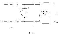
图11是用于说明根据本发明的示范性实施例的示范性显示面板的示范性触摸位置检测部分的示意性电路图。FIG. 11 is a schematic circuit diagram for explaining an exemplary touch position detection part of an exemplary display panel according to an exemplary embodiment of the present invention.
参考图1、6和11,基于从定时控制部分310(如图1中所示)输出的第五控制信号CNTL5驱动电压控制部分410来向第一和第二信号线SL1和SL2施加第一和第二初始驱动电压Vid1和Vid2。Referring to FIGS. 1, 6 and 11, the
当外部提供的压力PO使第一和第二信号线SL1和SL2彼此电连接时,施加给每条第一和第二信号线SL1和SL2的电压电平发生了变化。数据采样部分420将预定的参考信号Vref与每条第一和第二信号线SL1和SL2变化的电压电平相比较来放大参考信号Vref和每条第一和第二信号线SL1和SL2发生变化之间的电压差,并且产生第一和第二检测信号DS1和DS2。可以调整参考信号Vref以增强检测每条第一和第二信号线SL1和SL2的电平变化的灵敏度。数据采样部分420可以包括运算放大器(Op-Amp),且电源部分320可以输出参考信号Vref。When the pressure PO supplied from the outside electrically connects the first and second signal lines SL1 and SL2 to each other, the voltage level applied to each of the first and second signal lines SL1 and SL2 changes. The
例如,多个数据采样部分420可以连接每条第一和第二信号线SL1和SL2。电压控制部分410可以包括如金属氧化物半导体(“MOS”)晶体管的开关元件。电压控制部分410可以电连接第一和第二信号线SL1和SL2。For example, the plurality of
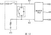
图12是用于说明根据本发明的另一示范性实施例的示范性显示面板的示范性触摸位置检测部分的示范性电路图。FIG. 12 is an exemplary circuit diagram for explaining an exemplary touch position detection part of an exemplary display panel according to another exemplary embodiment of the present invention.
参考图12,向第一信号线SL1施加第一初始驱动电压Vid1,而第二信号线SL2接地,使得施加给第二信号线SL2的电压为0V。第一初始驱动电压Vid1不是0V。Referring to FIG. 12, the first initial driving voltage Vid1 is applied to the first signal line SL1, and the second signal line SL2 is grounded, so that the voltage applied to the second signal line SL2 is 0V. The first initial driving voltage Vid1 is not 0V.
当外部提供的压力PO使第一和第二信号线SL1和SL2彼此电连接时,施加给每条第一和第二信号线SL1和SL2的电压电平改变。数据采样部分420将预定的参考信号Vref与每条第一和第二信号线SL1和SL2变化的电压电平相比较来放大参考信号Vref和每条第一和第二信号线SL1和SL2变化之间的电压差,并且产生第一和第二检测信号DS1和DS2。When the pressure PO supplied from the outside electrically connects the first and second signal lines SL1 and SL2 to each other, the voltage level applied to each of the first and second signal lines SL1 and SL2 changes. The
通过采用上述的示范性显示面板和显示设备,使在液晶显示器的触摸屏功能器件防止显示质量劣化的方法成为可能。该方法可以包括提供带有像素电极、公共电极、电连接第一信号线的第一感测电极和电连接第二信号线的第二感测电极的阵列基板,提供带有从其突出的导电连接部件的相对基板,在阵列基板和相对基板间设置液晶层,当液晶显示器工作时该液晶层中的液晶分子在阵列基板上水平取向,以及向相对基板施加外部提供的压力以在阵列基板上通过第一和第二感测电极使连接部件与第一和第二信号线相连,其中外部提供的压力基本不会改变液晶分子的取向。By adopting the above-mentioned exemplary display panel and display device, it becomes possible to prevent the deterioration of the display quality in the touch screen functional device of the liquid crystal display. The method may include providing an array substrate with a pixel electrode, a common electrode, a first sensing electrode electrically connected to a first signal line, and a second sensing electrode electrically connected to a second signal line, providing a conductive electrode protruding therefrom. The opposite substrate of the connection part, a liquid crystal layer is arranged between the array substrate and the opposite substrate, and the liquid crystal molecules in the liquid crystal layer are aligned horizontally on the array substrate when the liquid crystal display is in operation, and an externally provided pressure is applied to the opposite substrate to form a liquid crystal layer on the array substrate. The connection part is connected to the first and second signal lines through the first and second sensing electrodes, wherein the pressure provided from outside does not substantially change the orientation of the liquid crystal molecules.
根据以上描述,显示面板包括具有像素电极和公共电极的阵列基板。因此,当显示面板工作时,液晶分子在阵列基板上水平取向。因此,为了进行触摸屏功能,当向显示面板施加外部提供的压力时,基本不会改变阵列基板上液晶分子的取向,且可以改进显示质量。According to the above description, the display panel includes an array substrate having pixel electrodes and common electrodes. Therefore, when the display panel is in operation, the liquid crystal molecules are aligned horizontally on the array substrate. Therefore, when an externally provided pressure is applied to the display panel for the touch screen function, the orientation of the liquid crystal molecules on the array substrate is not substantially changed, and display quality can be improved.
此外,通过公共电压线施加用于进行感测工作的电压以简化用于驱动各条信号线的电压控制部分。In addition, the voltage for performing the sensing operation is applied through the common voltage line to simplify the voltage control section for driving the respective signal lines.
虽然以上具体描述了本发明的示范性实施例,但是应该理解,本发明并不仅局限于这些示范性实施例,但不脱离权利要求所确定的本发明的范围和精神可以进行多种改进和修改。Although the exemplary embodiments of the present invention have been described in detail above, it should be understood that the present invention is not limited to these exemplary embodiments, but various improvements and modifications can be made without departing from the scope and spirit of the present invention defined by the claims .
Claims (22)
Applications Claiming Priority (2)
| Application Number | Priority Date | Filing Date | Title |
|---|---|---|---|
| KR16077/06 | 2006-02-20 | ||
| KR1020060016077AKR101205539B1 (en) | 2006-02-20 | 2006-02-20 | Liquid crystal display panel and liquid crystal display panel having the same |
Publications (1)
| Publication Number | Publication Date |
|---|---|
| CN101038385Atrue CN101038385A (en) | 2007-09-19 |
Family
ID=38427665
Family Applications (1)
| Application Number | Title | Priority Date | Filing Date |
|---|---|---|---|
| CNA2007101035794APendingCN101038385A (en) | 2006-02-20 | 2007-02-25 | Liquid crystal display panel and liquid crystal display panel having the same |
Country Status (4)
| Country | Link |
|---|---|
| US (2) | US7903096B2 (en) |
| JP (1) | JP2007226217A (en) |
| KR (1) | KR101205539B1 (en) |
| CN (1) | CN101038385A (en) |
Cited By (15)
| Publication number | Priority date | Publication date | Assignee | Title |
|---|---|---|---|---|
| CN101900903A (en)* | 2009-05-29 | 2010-12-01 | 卡西欧计算机株式会社 | Liquid crystal display panel and liquid crystal display device |
| CN101943812A (en)* | 2009-07-01 | 2011-01-12 | 卡西欧计算机株式会社 | Display panels and touch panel |
| WO2011012035A1 (en)* | 2009-07-30 | 2011-02-03 | Byd Company Limited | Touchpad |
| CN102043535A (en)* | 2009-10-23 | 2011-05-04 | 三星电子株式会社 | Touch substrate and display device having the same |
| CN102193229A (en)* | 2010-03-19 | 2011-09-21 | 乐金显示有限公司 | Touch sensing type liquid crystal display device and its manufacture method |
| CN102193230A (en)* | 2010-03-19 | 2011-09-21 | 乐金显示有限公司 | Touch sensing type liquid crystal display device and method of fabricating the same |
| CN102346340A (en)* | 2010-08-03 | 2012-02-08 | 胜华科技股份有限公司 | Liquid crystal display panel |
| WO2013075540A1 (en)* | 2011-11-25 | 2013-05-30 | 上海天马微电子有限公司 | Imbedded touch screen liquid crystal display device and touch drive method thereof |
| CN104122697A (en)* | 2013-08-30 | 2014-10-29 | 深超光电(深圳)有限公司 | Touch-sensitive liquid crystal display panel and manufacturing method thereof |
| US8928598B2 (en) | 2009-06-12 | 2015-01-06 | Au Optronics Corporation | Touch-sensing liquid crystal display panel and liquid crystal display |
| US9218080B2 (en) | 2010-03-19 | 2015-12-22 | Lg Display Co., Ltd. | Touch sensing type liquid crystal display device including anti-static outer layer and method of fabricating the same |
| CN106200030A (en)* | 2015-04-30 | 2016-12-07 | 小米科技有限责任公司 | LCDs, pressure measurement method and device |
| CN107887410A (en)* | 2016-09-29 | 2018-04-06 | 株式会社日本显示器 | Display device |
| CN108021272A (en)* | 2016-10-31 | 2018-05-11 | 乐金显示有限公司 | Power sensing device further and the display device with the power sensing device further |
| CN111106153A (en)* | 2019-12-11 | 2020-05-05 | 上海天马有机发光显示技术有限公司 | A display panel, its manufacturing method and display device |
Families Citing this family (51)
| Publication number | Priority date | Publication date | Assignee | Title |
|---|---|---|---|---|
| FR2903207B1 (en)* | 2006-06-28 | 2008-11-07 | Jazzmutant Soc Par Actions Sim | MULTIPOINT TOUCH SENSOR WITH ACTIVE MATRIX |
| KR101297387B1 (en) | 2006-11-09 | 2013-08-19 | 삼성디스플레이 주식회사 | Liquid crystal display associated with touch panel |
| KR101385190B1 (en)* | 2007-02-07 | 2014-04-15 | 삼성디스플레이 주식회사 | Liquid crystal display and manufacturing method of the same |
| KR100879478B1 (en)* | 2007-10-16 | 2009-01-23 | 주식회사 티엘아이 | Touch screen liquid crystal display device for improving the contact position detection of the object and its driving method |
| KR101542397B1 (en)* | 2007-12-10 | 2015-08-06 | 삼성디스플레이 주식회사 | Display device having contact detection function and driving method thereof |
| KR20090075369A (en)* | 2008-01-04 | 2009-07-08 | 삼성전자주식회사 | Display panel |
| US8179482B2 (en)* | 2008-03-19 | 2012-05-15 | Samsung Electronics Co., Ltd. | Touch panel display and method of manufacturing the same |
| JP5212901B2 (en)* | 2008-09-25 | 2013-06-19 | ブラザー工業株式会社 | Glasses-type image display device |
| CN101713877A (en)* | 2008-10-08 | 2010-05-26 | 深超光电(深圳)有限公司 | Method for manufacturing multipoint touch liquid display panel |
| TWI417767B (en)* | 2008-10-17 | 2013-12-01 | Century Display Shenxhen Co | Method for manufacturing multi - touch liquid crystal display panel |
| JP2010108501A (en) | 2008-10-30 | 2010-05-13 | Samsung Electronics Co Ltd | Touch screen controller having increased sensing sensitivity, and display driving circuit and display device and system having the touch screen controller |
| KR101513440B1 (en) | 2008-12-01 | 2015-04-22 | 삼성디스플레이 주식회사 | Touch screen display device and manufacturing method thereof |
| US20120013593A1 (en)* | 2009-03-17 | 2012-01-19 | Sharp Kabushiki Kaisha | Display device |
| KR101551447B1 (en)* | 2009-04-27 | 2015-09-09 | 삼성디스플레이 주식회사 | Display panel, display device having the same, and driving method of the display device |
| TWI406159B (en)* | 2009-05-13 | 2013-08-21 | Chimei Innolux Corp | Touch panel and touch display device |
| TWI396891B (en)* | 2009-06-04 | 2013-05-21 | Au Optronics Corp | Touch panel and method for manufacturing the same |
| JP5389923B2 (en)* | 2009-07-31 | 2014-01-15 | シャープ株式会社 | Liquid crystal panel and liquid crystal display device |
| US8120589B2 (en)* | 2009-09-11 | 2012-02-21 | Century Display(ShenZhen)Co., Ltd. | Touch panel |
| TW201111859A (en)* | 2009-09-17 | 2011-04-01 | Novatek Microelectronics Corp | Touch apparatus and display panel thereof |
| KR101588347B1 (en) | 2009-09-28 | 2016-01-26 | 삼성디스플레이 주식회사 | Liquid crystal display panel, liquid crystal display device including same, and driving method of liquid crystal display device |
| TWI408449B (en)* | 2009-11-03 | 2013-09-11 | Wintek Corp | Liquid crystal display panel |
| CN101738770B (en)* | 2009-12-28 | 2012-04-25 | 友达光电(苏州)有限公司 | A liquid crystal display panel and touch detection method thereof |
| KR101686094B1 (en)* | 2009-12-31 | 2016-12-13 | 엘지디스플레이 주식회사 | Liquid Crystal Display Device and Method for Manufacturing the Same |
| KR101735568B1 (en)* | 2010-03-30 | 2017-05-15 | 엘지디스플레이 주식회사 | Color filter array substrate, liquid crystal display device comprising the same, and method for manufacturing the same |
| KR101761861B1 (en) | 2010-06-18 | 2017-07-27 | 삼성디스플레이 주식회사 | Touch sensible display device |
| KR101726739B1 (en) | 2010-12-21 | 2017-04-14 | 삼성디스플레이 주식회사 | Touch display substrate and touch display panel having the same |
| US9417754B2 (en) | 2011-08-05 | 2016-08-16 | P4tents1, LLC | User interface system, method, and computer program product |
| JP5906043B2 (en)* | 2011-09-01 | 2016-04-20 | 株式会社ジャパンディスプレイ | Liquid crystal display |
| US9195331B2 (en)* | 2011-12-06 | 2015-11-24 | Apple Inc. | Common electrode connections in integrated touch screens |
| US8982310B2 (en)* | 2011-12-15 | 2015-03-17 | Apple Inc. | Displays with light-curable sealant |
| KR101524449B1 (en) | 2011-12-22 | 2015-06-02 | 엘지디스플레이 주식회사 | Liquid crystal display device and Method for manufacturing the same |
| KR20130115621A (en)* | 2012-04-12 | 2013-10-22 | 삼성디스플레이 주식회사 | Display device and fabrication method of the same |
| KR101373953B1 (en)* | 2012-07-20 | 2014-03-12 | 엘지디스플레이 주식회사 | Touch sensor integrated display device |
| CN103631426B (en)* | 2012-08-26 | 2016-12-21 | 宸鸿科技(厦门)有限公司 | Contact panel and manufacture method thereof |
| KR102180088B1 (en)* | 2013-12-31 | 2020-11-18 | 삼성디스플레이 주식회사 | Display panel and display apparatus having them |
| US9523896B2 (en) | 2014-04-03 | 2016-12-20 | Apple Inc. | Border masking structures for liquid crystal displays |
| CN105022184A (en)* | 2014-04-17 | 2015-11-04 | 株式会社日本显示器 | Display device |
| CN103970353B (en)* | 2014-04-29 | 2016-10-05 | 京东方科技集团股份有限公司 | A kind of touch-control display panel and touch control display apparatus |
| CN104035615B (en)* | 2014-05-20 | 2016-03-02 | 京东方科技集团股份有限公司 | A kind of touch display panel and display device |
| KR102250847B1 (en)* | 2014-11-13 | 2021-05-13 | 삼성디스플레이 주식회사 | Display device intergrated touch screen panel |
| KR101615499B1 (en)* | 2015-04-28 | 2016-04-27 | 엘지디스플레이 주식회사 | Liquid crystal display device and Method for manufacturing the same |
| CN104808403B (en)* | 2015-05-08 | 2018-05-15 | 厦门天马微电子有限公司 | Array base palte, display panel and display device |
| US9977276B2 (en)* | 2015-05-08 | 2018-05-22 | Xiamen Tianma Micro-Electronics Co., Ltd. | Array substrate, display panel and display device |
| CN104900658B (en) | 2015-06-15 | 2018-07-27 | 京东方科技集团股份有限公司 | Touch panel and preparation method thereof, touch control display apparatus |
| CN105093582A (en)* | 2015-08-12 | 2015-11-25 | 小米科技有限责任公司 | Method and device for detecting pressure in mobile terminal |
| CN105116584B (en)* | 2015-09-16 | 2017-02-22 | 深圳市华星光电技术有限公司 | Liquid crystal display panel and device |
| CN105242470B (en)* | 2015-11-09 | 2018-09-11 | 武汉华星光电技术有限公司 | A kind of liquid crystal display panel and liquid crystal display device |
| CN105528120B (en)* | 2016-03-04 | 2018-09-14 | 京东方科技集团股份有限公司 | Display base plate and its driving method, display device |
| CN106201075B (en)* | 2016-06-30 | 2019-06-25 | 京东方科技集团股份有限公司 | Touch panel and its driving method, touch control display apparatus |
| CN114730543B (en)* | 2020-11-05 | 2024-01-19 | 京东方科技集团股份有限公司 | Display substrate and detection method, preparation method and display device thereof |
| JP2024032250A (en)* | 2022-08-29 | 2024-03-12 | 株式会社ジャパンディスプレイ | LCD display device with optical sensor |
Family Cites Families (9)
| Publication number | Priority date | Publication date | Assignee | Title |
|---|---|---|---|---|
| JP2888177B2 (en)* | 1994-09-28 | 1999-05-10 | 日本電気株式会社 | Liquid crystal display |
| JPH10123534A (en)* | 1996-10-23 | 1998-05-15 | Toshiba Corp | Liquid crystal display device |
| JP2000099268A (en)* | 1998-09-21 | 2000-04-07 | Nec Eng Ltd | Liquid crystal display device with coordinate position detecting function |
| JP2001075074A (en) | 1999-08-18 | 2001-03-23 | Internatl Business Mach Corp <Ibm> | Touch sensor type liquid crystal display device |
| US6753853B1 (en)* | 2000-09-29 | 2004-06-22 | Rockwell Automation Technologies, Inc. | Low power dissipation touch plane interface circuit |
| KR100499576B1 (en)* | 2003-03-28 | 2005-07-05 | 엘지.필립스 엘시디 주식회사 | In-Plane Switching mode Liquid Crystal Display Device Having Touch Panel of Electro Magnetic Type |
| US7755616B2 (en)* | 2003-03-28 | 2010-07-13 | Lg Display Co., Ltd. | Liquid crystal display device having electromagnetic type touch panel |
| US7196696B2 (en)* | 2004-03-19 | 2007-03-27 | Tsung-Ying Li | Position touch screen panel and method of arranging a resistive sensing circuit thereof |
| KR101226440B1 (en)* | 2005-09-26 | 2013-01-28 | 삼성디스플레이 주식회사 | Display panel and display device having the same and method of detecting touch position of the display device |
- 2006
- 2006-02-20KRKR1020060016077Apatent/KR101205539B1/ennot_activeExpired - Fee Related
- 2007
- 2007-02-05JPJP2007025218Apatent/JP2007226217A/enactivePending
- 2007-02-15USUS11/675,131patent/US7903096B2/ennot_activeExpired - Fee Related
- 2007-02-25CNCNA2007101035794Apatent/CN101038385A/enactivePending
- 2011
- 2011-02-01USUS13/018,540patent/US8373675B2/ennot_activeExpired - Fee Related
Cited By (36)
| Publication number | Priority date | Publication date | Assignee | Title |
|---|---|---|---|---|
| CN101900903A (en)* | 2009-05-29 | 2010-12-01 | 卡西欧计算机株式会社 | Liquid crystal display panel and liquid crystal display device |
| CN101900903B (en)* | 2009-05-29 | 2014-09-10 | 卡西欧计算机株式会社 | Liquid crystal display panel and liquid crystal display apparatus |
| US8928598B2 (en) | 2009-06-12 | 2015-01-06 | Au Optronics Corporation | Touch-sensing liquid crystal display panel and liquid crystal display |
| CN101943812B (en)* | 2009-07-01 | 2014-06-25 | 卡西欧计算机株式会社 | Liquid crystal display panel and touch panel |
| CN101943812A (en)* | 2009-07-01 | 2011-01-12 | 卡西欧计算机株式会社 | Display panels and touch panel |
| US8624854B2 (en) | 2009-07-01 | 2014-01-07 | Casio Computer Co., Ltd. | Liquid crystal display panel and touch panel |
| WO2011012035A1 (en)* | 2009-07-30 | 2011-02-03 | Byd Company Limited | Touchpad |
| US8411065B2 (en) | 2009-07-30 | 2013-04-02 | BYD Company Ltd. | Touchpad with a double-layer printed circuit board structure |
| CN102043535A (en)* | 2009-10-23 | 2011-05-04 | 三星电子株式会社 | Touch substrate and display device having the same |
| US9830038B2 (en) | 2009-10-23 | 2017-11-28 | Samsung Display Co., Ltd. | Touch substrate, method of manufacturing the same and display device having the same |
| CN102043535B (en)* | 2009-10-23 | 2016-03-30 | 三星显示有限公司 | Touch substrate and the display device with this touch substrate |
| US9239651B2 (en) | 2009-10-23 | 2016-01-19 | Samsung Display Co., Ltd. | Touch substrate, method of manufacturing the same and display device having the same |
| US9218080B2 (en) | 2010-03-19 | 2015-12-22 | Lg Display Co., Ltd. | Touch sensing type liquid crystal display device including anti-static outer layer and method of fabricating the same |
| US10620729B2 (en) | 2010-03-19 | 2020-04-14 | Lg Display Co., Ltd. | Touch sensing type liquid crystal display device and method of fabricating the same |
| US12130976B2 (en) | 2010-03-19 | 2024-10-29 | Lg Display Co., Ltd. | Touch sensing type display device |
| CN102193230B (en)* | 2010-03-19 | 2014-12-03 | 乐金显示有限公司 | Touch sensing type liquid crystal display device and method of fabricating the same |
| US8704962B2 (en) | 2010-03-19 | 2014-04-22 | Lg Display Co., Ltd. | Touch sensing type liquid crystal display device comprising a touch sensing unit that includes X and Y direction sensing lines and a plurality of touch blocks |
| CN102193229B (en)* | 2010-03-19 | 2015-07-29 | 乐金显示有限公司 | Touch-sensing formula Liquid crystal disply device and its preparation method |
| US11907460B2 (en) | 2010-03-19 | 2024-02-20 | Lg Display Co., Ltd. | Touch sensing type display device |
| US11620009B2 (en) | 2010-03-19 | 2023-04-04 | Lg Display Co., Ltd. | Touch sensing type display device |
| CN102193230A (en)* | 2010-03-19 | 2011-09-21 | 乐金显示有限公司 | Touch sensing type liquid crystal display device and method of fabricating the same |
| US11016594B2 (en) | 2010-03-19 | 2021-05-25 | Lg Display Co., Ltd. | Touch sensing type display device and method of fabricating the same |
| CN102193229A (en)* | 2010-03-19 | 2011-09-21 | 乐金显示有限公司 | Touch sensing type liquid crystal display device and its manufacture method |
| US9600109B2 (en) | 2010-03-19 | 2017-03-21 | Lg Display Co., Ltd. | Touch sensing type liquid crystal display device and method of fabricating the same |
| US9727158B2 (en) | 2010-03-19 | 2017-08-08 | Lg Display Co., Ltd. | Touch sensing type liquid crystal display device and method of fabricating the same |
| CN102346340B (en)* | 2010-08-03 | 2014-06-18 | 胜华科技股份有限公司 | LCD panel |
| CN102346340A (en)* | 2010-08-03 | 2012-02-08 | 胜华科技股份有限公司 | Liquid crystal display panel |
| US9442330B2 (en) | 2011-11-25 | 2016-09-13 | Shanghai Tianma Micro-electronics Co., Ltd. | Embedded touch screen liquid crystal display device and touch drive method thereof |
| WO2013075540A1 (en)* | 2011-11-25 | 2013-05-30 | 上海天马微电子有限公司 | Imbedded touch screen liquid crystal display device and touch drive method thereof |
| CN104122697A (en)* | 2013-08-30 | 2014-10-29 | 深超光电(深圳)有限公司 | Touch-sensitive liquid crystal display panel and manufacturing method thereof |
| CN106200030A (en)* | 2015-04-30 | 2016-12-07 | 小米科技有限责任公司 | LCDs, pressure measurement method and device |
| CN107887410A (en)* | 2016-09-29 | 2018-04-06 | 株式会社日本显示器 | Display device |
| CN107887410B (en)* | 2016-09-29 | 2021-09-28 | 株式会社日本显示器 | Display device |
| CN108021272A (en)* | 2016-10-31 | 2018-05-11 | 乐金显示有限公司 | Power sensing device further and the display device with the power sensing device further |
| CN108021272B (en)* | 2016-10-31 | 2024-02-02 | 乐金显示有限公司 | Force sensing device and display device having the same |
| CN111106153A (en)* | 2019-12-11 | 2020-05-05 | 上海天马有机发光显示技术有限公司 | A display panel, its manufacturing method and display device |
Also Published As
| Publication number | Publication date |
|---|---|
| KR20070082959A (en) | 2007-08-23 |
| US20110122084A1 (en) | 2011-05-26 |
| KR101205539B1 (en) | 2012-11-27 |
| US20070195029A1 (en) | 2007-08-23 |
| US7903096B2 (en) | 2011-03-08 |
| JP2007226217A (en) | 2007-09-06 |
| US8373675B2 (en) | 2013-02-12 |
Similar Documents
| Publication | Publication Date | Title |
|---|---|---|
| CN101038385A (en) | Liquid crystal display panel and liquid crystal display panel having the same | |
| CN102445780B (en) | Liquid crystal display device with interred touch screen | |
| CN1285951C (en) | Active matrix base plate and display device | |
| CN1955823A (en) | Liquid crystal display and method thereof | |
| KR101710407B1 (en) | Liquid crystal display device with a built in touch screen and driving mehtod thereof | |
| JP2007128091A (en) | Display substrate, manufacturing method thereof, and display panel including the same | |
| CN106328077A (en) | Display device and mobile terminal using the same | |
| CN1734322A (en) | Array base palte and have the main substrate and the liquid crystal indicator of described array base palte | |
| CN1904992A (en) | Display device, method of driving the same and driving device for driving the same | |
| KR101843462B1 (en) | Liquid crystal display apparatus comprising a touch screen | |
| KR102020938B1 (en) | Liquid crystal display | |
| CN1885125A (en) | Backlight assembly, display device having the same, and assembling method thereof | |
| CN1932626A (en) | Liquid crystal display device | |
| CN107015679B (en) | Display device having a touch screen therein | |
| CN1924652A (en) | Liquid crystal display including sensing unit | |
| CN1908787A (en) | LCD Monitor | |
| CN1773335A (en) | Display device including sensing element | |
| CN1955824A (en) | Liquid crystal display device | |
| CN1991534A (en) | Liquid crystal display | |
| US20120171425A1 (en) | Display panel | |
| CN1536421A (en) | Liquid crystal display device | |
| CN1540400A (en) | Liquid crystal display device having a plurality of pixel electrodes | |
| CN1959507A (en) | Array substrate | |
| CN112667099A (en) | Touch display device and display panel | |
| KR20120106214A (en) | Liquid crystal display device with a built in touch screen and driving mehtod thereof |
Legal Events
| Date | Code | Title | Description |
|---|---|---|---|
| C06 | Publication | ||
| PB01 | Publication | ||
| C10 | Entry into substantive examination | ||
| SE01 | Entry into force of request for substantive examination | ||
| C02 | Deemed withdrawal of patent application after publication (patent law 2001) | ||
| WD01 | Invention patent application deemed withdrawn after publication | Application publication date:20070919 |