CN101036232A - Thin film transistor with semiconductor characteristic multi-cation oxide channel and manufacturing method - Google Patents
Thin film transistor with semiconductor characteristic multi-cation oxide channel and manufacturing methodDownload PDFInfo
- Publication number
- CN101036232A CN101036232ACNA2005800341683ACN200580034168ACN101036232ACN 101036232 ACN101036232 ACN 101036232ACN A2005800341683 ACNA2005800341683 ACN A2005800341683ACN 200580034168 ACN200580034168 ACN 200580034168ACN 101036232 ACN101036232 ACN 101036232A
- Authority
- CN
- China
- Prior art keywords
- film transistor
- oxide
- thin film
- patterning
- depositing
- Prior art date
- Legal status (The legal status is an assumption and is not a legal conclusion. Google has not performed a legal analysis and makes no representation as to the accuracy of the status listed.)
- Granted
Links
Images


Classifications
- H—ELECTRICITY
- H10—SEMICONDUCTOR DEVICES; ELECTRIC SOLID-STATE DEVICES NOT OTHERWISE PROVIDED FOR
- H10D—INORGANIC ELECTRIC SEMICONDUCTOR DEVICES
- H10D30/00—Field-effect transistors [FET]
- H10D30/60—Insulated-gate field-effect transistors [IGFET]
- H10D30/67—Thin-film transistors [TFT]
- H10D30/674—Thin-film transistors [TFT] characterised by the active materials
- H10D30/6755—Oxide semiconductors, e.g. zinc oxide, copper aluminium oxide or cadmium stannate
- H—ELECTRICITY
- H10—SEMICONDUCTOR DEVICES; ELECTRIC SOLID-STATE DEVICES NOT OTHERWISE PROVIDED FOR
- H10D—INORGANIC ELECTRIC SEMICONDUCTOR DEVICES
- H10D30/00—Field-effect transistors [FET]
- H10D30/60—Insulated-gate field-effect transistors [IGFET]
- H10D30/67—Thin-film transistors [TFT]
- H10D30/6729—Thin-film transistors [TFT] characterised by the electrodes
- H10D30/6737—Thin-film transistors [TFT] characterised by the electrodes characterised by the electrode materials
- H10D30/6739—Conductor-insulator-semiconductor electrodes
- H—ELECTRICITY
- H10—SEMICONDUCTOR DEVICES; ELECTRIC SOLID-STATE DEVICES NOT OTHERWISE PROVIDED FOR
- H10D—INORGANIC ELECTRIC SEMICONDUCTOR DEVICES
- H10D62/00—Semiconductor bodies, or regions thereof, of devices having potential barriers
- H10D62/10—Shapes, relative sizes or dispositions of the regions of the semiconductor bodies; Shapes of the semiconductor bodies
- H10D62/117—Shapes of semiconductor bodies
- H10D62/118—Nanostructure semiconductor bodies
- H10D62/119—Nanowire, nanosheet or nanotube semiconductor bodies
- H10D62/121—Nanowire, nanosheet or nanotube semiconductor bodies oriented parallel to substrates
- H—ELECTRICITY
- H10—SEMICONDUCTOR DEVICES; ELECTRIC SOLID-STATE DEVICES NOT OTHERWISE PROVIDED FOR
- H10D—INORGANIC ELECTRIC SEMICONDUCTOR DEVICES
- H10D99/00—Subject matter not provided for in other groups of this subclass
Landscapes
- Thin Film Transistor (AREA)
Abstract
Description
Technical field
Relate generally to thin-film transistor of the present invention and manufacture method thereof.
Background technology
(for example: silicon, electron level glass) technology is compared, and (for example: plastics) going up the formation circuit will reduce cost significantly at low-cost backing material with using expensive substrate.In order to obtain such low-cost advantage, need (for example: transistor) produce the high-performance electronic device with the technology that is suitable for low-cost backing material.A typical embodiments that benefits from the application of this high performance device is the display base plate.
Usually, alternative inexpensive substrate material (for example: organic substance and inexpensive glass) is also responsive especially to temperature.Therefore, in the high-performance electronic device manufacturing process, necessarily can not make backing material be subjected to high temperature.Usually, it is desirable to treatment temperature and can not surpass about 100 ℃~about 300 ℃ of scopes.The inexpensive substrate material can use usually at a lower temperature.For example, can be with various organic semiconductors and insulator structure transistor under very low temperature, the suitable low temperature inexpensive substrate material that uses under this temperature.And organic semiconductor shows good mechanical flexibility usually, and this is very important when it combines with flexible substrate material.Yet because the intrinsic limitation of material, the organic semi-conductor mobility is very low usually (for example: about 1cm2/ VS, perhaps in addition lower), this has just reduced it and has been used for the applicability of high-performance, large-area devices as display.Equally, low mobility has also limited the applicability of amorphous silicon.Although OTFT (TFT ' s), in some cases, be fit to pixel transitions element (as: bistable display technologies), but they are not suitable for glass-based (on-glass) driver or other treatment circuit usually, and the glass-based driver can be integrated further to reduce the display cost on the whole.Except the cost of material is low than other, plastic also had elasticity, antidetonation, the advantage of light weight.
Another method relate to the more conventional inorganic semiconductor of use (for example: silicon), the treatment temperature that it is had relatively high expectations.Elder generation's high-temperature process semiconductor carries out switch process again, and the semiconductor nanowires that will handle in this switch process, nano belt or other similar structures change into low-cost backing material.For example, paper " using the high performance thin film transistor (High-performance thin-film transistors using semiconductornanowires and nanoribbons) of semiconductor nanowires and nano belt ", Nature, v.425, (on September 18th, 2003) 274-278 page or leaf, the mobility that people such as X.Duan have reported with the silicon nanowires thin-film transistor on plastics of the method manufacturing is higher than 100cm2/ VS.Although this method has realized high mobility and excellent performance, based on the characteristic of conversion process, process complexity has increased, and therefore to a certain extent, the substrate relevant cost that is reduced is increased by process complexity and the cost that brings is offset.
Also can on the low-temperature substrate material, directly deposit and handle some inorganic semiconductor.Can under the temperature that is fit to the plastic material, directly process amorphous silicon film transistor.For example, report once, during about 180 ℃ of maximum processing temperature, mobility is about 0.4cm2/ VS (people such as S.H.Won, IEEE Electron Device Letters, v.25, and n.3, (in March, 2004), 132-134 page or leaf).Yet amorphous silicon has the limitation on the mobility limitation that is similar to above-mentioned OTFT and the associated applicability.Utilize the laser crystallization method, also can go up and directly handle polycrystalline SiTFT at " plastics "; For example, report once, during 320 ℃ of maximum processing temperatures, mobility is approximately 65cm2/ VS (people such as F.Lemmi, IEEE Electron Device Letters, v.25, and n.7, (in July, 2004), 486-488 page or leaf).
Reporting in the past, also is to utilize the laser crystallization method, and under 150 ℃ of the maximum processing temperatures, the mobility of polycrystalline SiTFT is 60cm2/ VS, people such as S.D.Theiss, " on flexible plastic substrate, making polycrystalline SiTFT (100 ℃ of on a of Polysilicon Thin FilmTransistors Fabricated at Flexible Plastic Substrate) under 100 ℃ " IEDM Technical Digest (1998) 257-260 pages or leaves.The complexity that increases cost and laser crystallization method is the potential shortcoming of the method.
Although these existing methods can obtain useful device, also need less film apparatus and the manufacture method thereof that is subjected to low performance, process complexity and/or treatment temperature restriction.
Description of drawings
Read following detailed description in conjunction with the drawings, those skilled in the art are readily appreciated that feature of the present invention and advantage.Wherein:
Fig. 1 is the flow chart of a method for fabricating thin film transistor embodiment.
Fig. 2 is the vertical view of a thin-film transistor specific embodiments.
Fig. 3 is the cross-sectional elevational view of a thin-film transistor embodiment.
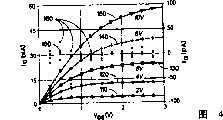
Fig. 4 is that the leakage current of a thin-film transistor embodiment and gate current are with the drain voltage change curve.
Fig. 5 is that the leakage current of representing with logarithmic coordinates of a thin-film transistor embodiment and gate current are with the gate voltage change curve.
Fig. 6 is that the mobility of a thin-film transistor embodiment is with the gate voltage change curve.
Fig. 7 for the mobility of each transistor embodiment of various channel compositions making with the annealing temperature change curve.
The detailed description of embodiment
In order clearly to describe, accompanying drawing is not by unified scale.Especially, the vertical and horizontal ratio of same accompanying drawing may be different, and the ratio of different accompanying drawings also may be different.For this consideration, adopted directional terminology (for example: " top ", " bottom ", " preceding ", " back ", " front portion ", " afterbody " etc.) to indicate the orientation of described accompanying drawing.Because assembly of the present invention can be positioned on each different direction, employed directional terminology is to be used to illustrate and non-limiting purpose.
The related periodic table of elements is based on the periodic table of being recommended by IUPAC (IUPAC).The latest edition of this periodic table can be obtained from the Internet, and network address is:Http:// www.iupac.org/reports/periodic_table/
One aspect of the present invention provides the embodiment of a thin-film transistor (TFT) 10, its manufacture method is as follows: substrate is provided, deposition and pattern metal grid on substrate, with the metal gates anodization of patterning to form gate insulator thereon, deposition and patterning comprise the channel layer of polycation oxide, deposition and pattern conductive source electrode and conductive drain.
Another aspect of the present invention comprises the manufacture method of thin-film transistor (TFT).Fig. 1 is the flow chart of a manufacturing thin-film transistor method embodiment.The step of this method embodiment Reference numeral S10, S20 ... S80 represents.These Reference numerals do not show that these steps should carry out according to specific order (as: numerical order).Yet, can carry out these steps according to described order.Also indicate with the arrow in Fig. 1 flow chart in optional path.
An embodiment that is used to make the method for thin-film transistor (TFT) comprises the steps: to provide substrate, deposition and patterning can be by anodized metal gates, with the metal gates anodization of patterning to form gate insulator thereon, deposition and patterning comprise the channel layer of polycation oxide, deposition and pattern conductive source electrode and conductive drain.The method also can be included on the metal gates form after the gate insulator, deposition is as after the polycation oxide of channel layer or the annealing steps of choosing wantonly after the patterning channel layer.The details of the various embodiments of the method will be described in detail below.
In these method embodiments, if the required attribute of used specific backing material marked change can not take place being equal to or less than under about 400 ℃ of temperature, then these steps can be carried out under this temperature usually.The all material of Shi Yonging can place under 400 ℃ at least and handle the short time in this embodiment.Yet, do not need 400 ℃ of so high temperature usually.It will be appreciated that in the example of Miao Shuing that hereinafter the suitable temperature range of carrying out these steps comprises and is equal to or less than about 125 ℃ temperature.
Among the step S10, provide a kind of substrate.This substrate can be the substrate of flexible substrate and/or substantially transparent.In a lot of the application, polyimides (polyimide) film all is suitable substrate.An example of this film is Kapton HN, can be from DuPont High PerformanceFilms of Circleville, and Ohio (E.I.du Pont de Nemours and Company ofWilmington, the branch company of Delaware) obtains.And at least one embodiment, substrate is made up of one or more metals, can use insulating barrier (for example: polyimides) as the top coat of metallic substrates.Therefore, in some applications, substrate can be composite material (for example: the polyimide layer that applies) at stainless steel-based the end.Other suitable backing material for example comprises: rigid substrate, and silicon for example, silicon dioxide (quartz), aluminium oxide (for example: sapphire), perhaps one or more glass; And flexible substrate, comprise stainless steel and/or metal forming, and one or more organic backing materials, for example: acrylate, polyethylene terephthalate (PET), polyether sulfone (PES), Merlon (PC), Polyethylene Naphthalate (PEN), or poly-(methyl methacrylate) is (PMMA).The example of the compound substrate that another is suitable has the suprabasil polyimide coating of acrylate.
Among the step S20, deposition can anodized metal level.For example, but the anodized metal layer can comprise aluminium, tantalum, titanium, tungsten, or the alloy of these metals, or other any can anodized metal, condition is that the described metal gained of anodization oxide-film shows the attribute that is suitable for as the thin-film transistor gate insulator.Usually, if the resistance coefficient of this layer is enough low, metal is continuous film, and covers all surface defective of substrate, has enough excessive metal to consume (oxidation) in order to part simultaneously in anodizing process, and then its thickness is unimportant.For example, on the enough smooth and flawless substrate, the suitable thickness of aluminium is 200~500 nanometers.
Among the step S30, can anodized metal layer patternization to form metal gates.For example, can come the pattern metal grid with the photoetching process of any routine.
Among the step S40,, form gate insulator on its surface with the metal gates anodization.Anodization is the known method that forms oxide layer on metal, and it is in electrolytic cell, is anode with the metal, and makes the electrolytic cell energising.With aluminium is example, in the anodizing process, current density should be maintained at about 0.5 milliampere/cm usually2Below.Electrolytic cell can contain acid () the aqueous solution for example: citric acid, boric acid, tartaric acid, sulfuric acid, chromic acid, or oxalic acid for anodization.Aluminium and tantalum are usually with the anodized metal of this anodization method.Tungsten and titanium or other metal also can be electroplated.Randomly, can after anodization step S40, carry out annealing steps S45.Annealing steps S45 can be made of following step: the promptly dry structure of partly having finished that comprises anodized grid.
Among the step S50, deposition polycation oxide skin(coating).It is believed that the polycation oxide provides such channel material, this channel material keeps amorphous state in the temperature range of handling and using.Yet, can not think that the present invention is subjected to the limitation of any particular theory of operation.
Can use multiple polycation oxide, for example: the periodic table ofelements
For example, in the embodiment of zinc-indium oxide as the polycation oxide, the atomic ratio of zinc and indium is between about 1: 1 to about 1: 8.In other particular, the atomic ratio of zinc and indium can be about 1: 2 to about 1: 6.In a kind of alternative suitable embodiment, zinc and phosphide atom ratio are approximately 1: 4 (ZnO and In accordingly,2O3Mol ratio is approximately 1: 2).Represent that in the mode of mol ratio composition does not show ZnO and In2O3Independently to be present in mutually in the polycation oxide skin(coating).
Among the step S50, can form the polycation oxide skin(coating) with deposition at sputter polycation oxide on the part of grid pole insulating barrier at least.For example, can be by (for example: the target that comprises zinc-indium oxide) sputter is carried out in sputter from single target of comprising the polycation oxide; Perhaps, carry out reactive sputtering (i.e. sputter aerobic environment) by single metal target from the alloy that comprises required metal.For example, alternatively, can also be by two or more target associating sputters (for example: the target and the target that contains indium oxide that contain zinc oxide) that comprise different cation oxides; Perhaps, carry out reactive sputtering by two or more metallic targets.For consistent with temperature range discussed above, sputter can be carried out being equal to or less than under about 400 ℃ of temperature; In some cases, can carry out being equal to or less than under about 125 ℃ of temperature.Randomly, after deposition step S50, can carry out annealing steps S55, this is for the consideration that is consistent with other step temperature.
Among the step S60, patterning polycation oxide channel layer.Still can be by conventional photoetching process, perhaps other technology (for example: ion beam milling, laser ablation) is carried out patterning.Randomly, can carry out annealing steps S70 after patterning step S60, this is for the consideration that is consistent with other step temperature.
Among the step S80, deposition and pattern conductive source electrode and conductive drain.For example, this step can be finished by deposition and patterning indium-tin-oxide (ITO).For example, ITO can deposit and reach about 50-300 nano thickness and use conventional photoetching process patterning.Source electrode and drain material that other is suitable comprise doped oxide semiconductors, n type doping zinc-oxide for example, and indium oxide, and/or tin oxide, and/or metal, as Al, Ag, In, Sn, Zn, Ti, Mo, Au, Pd, Pt, Cu, Ni and W.
Another aspect of the present invention be in thin-film transistor with the method for polycation oxide as channel material: substrate is provided, deposition and pattern metal grid, on metal gates, form gate insulator, with polycation oxidate and patterning to form the channel layer of thin-film transistor.Deposition and transistorized conductive source of patterned film and conductive drain are made the thin-film transistor that uses the polycation oxide by this.
According to specific embodiment, those skilled in the art can more be expressly understood method of the present invention.One exemplary comprises the steps: to provide flexible substrate with zinc-indium oxide as the method for polycation oxide channel made thin-film transistor (TFT) on flexible substrate, deposition is fit to by anodized metal film on flexible substrate, metal film patternization is formed metal gates, with patterned metal gates anodization to form gate insulator thereon, randomly anneal, deposition comprises the channel layer of zinc-indium oxide, randomly annealing, with this channel layer patterning, randomly annealing, deposition and patterning comprise indium-tin-oxide (ITO) and form conductive source and conductive drain, deposition and patterning respectively with metal gates, the conductive contact pad that conductive source and conductive drain are electrically connected.
Usually, in this exemplary method, needn't all when the annealing steps of pointing out to choose wantonly, anneal at every turn.For example, can be only once just enough in deposition and patterning zinc-indium oxide channels layer after annealing.As above-mentioned, the annealing steps after the metal gates anodization of patterning can be comprised and will comprise that the structure that the part of carrying out anodized grid is finished carries out drying.This annealing steps may further include from gate insulating film remove do not have the anodizing process combination, residual organic.
Therefore, another aspect of the present invention provides the embodiment that forms thin-film transistor (TFT) 10 with said method on substrate.Fig. 2 is the top plan of the thin-film transistor embodiment of these methods manufacturings of a usefulness, and Fig. 3 is its cross-sectional elevational view.As shown in Figures 2 and 3, thin-film transistor comprises themetal gates 30 that is arranged on thesubstrate 20,metal gates 30 anodization is formed thegate insulator 40 that it is covered to small part.As shown in Figures 2 and 3, thin-film transistor also comprises the polycation oxide material is arranged on thechannel layer 70 that forms on the part of gridpole insulating barrier 40 at least, be separated from each other and all with theconductive source 50 and theconductive drain 60 ofpassage 70 adjacency.Common source electrode 50 and thegap 100 that drains between 60 define width of channel.Conductive contact pad source electrode 50 anddrain electrode 60 respectively.The 3rd conductive contact pad (not shown) can be electrically coupled to metal gates 30 (outside Fig. 3 sectional view).For example, those skilled in the art will know that these contact mats, and be not that each thin film transistor device of integrated circuit all needs usually just to convenient test.
In said method is described, obviously,substrate 20 can be flexible membrane (for example: polyimide film) and/or can be substantially transparent.Two or more cationic mixed oxides in the polycation oxide containing element periodic table ofpassage 70 in 11,12,13,14 and 15 families, for example, mixed oxide comprises and is selected from copper, silver, lead, germanium, antimony, gallium, cadmium, zinc, two or more cations in indium and the tin.The polycation oxide can be an amorphous state.Especially, the polycation oxide can be to be selected from gallium, cadmium, zinc, the cationic mixed oxide of indium and tin, for example zinc-indium oxide.The atomic ratio of zinc and indium can be about 1: 1 to about 1: 8 in this zinc-indium oxide channels material, is limited to about 1: 2 to about 1: 6 perhaps narrowlyer.Suitable atomic ratio is about 1: 4.This atom composition is not considered oxygen and the existence that reaches other optional elements.It only represents the relative scale of zinc and indium.
Metal gates comprises can anodized metal (for example: aluminium, tantalum, titanium, tungsten) or the alloy of these metals.Gate insulator comprise can anodized metal oxide (for example: aluminium oxide, tantalum oxide, titanium oxide, tungsten oxide) or the combination of these oxides.As mentioned above, conductive source or conductive drain or both can comprise the indium-tin-oxide (ITO) of substantially transparent.
Fig. 4,5 and 6 have shown by aluminium gate, the test result of the thin-film transistor that aluminium oxide gate insulator that anodization forms and zinc-indium oxide channels is formed.Fig. 4, in 5 and 6 embodiments of being explained, the stoichiometric proportion of zinc-indium oxide is 1: 4 Zn: In (atomic ratio).In these thin-film transistors each all comprises: be arranged on the metallic aluminium grid on the substrate, the anodization of metallic aluminium grid is formed, cover the aluminium oxide gate insulator on the metallic aluminium grid, the passage (be arranged on partial oxidation aluminium gate insulating barrier on) at least that comprises zinc-indium oxide, indium-tin-oxide (ITO) conductive source and the conductive drain that are separated from each other and all are provided with channels abut.Conductive metal gate plays a part to regulate conduction electron concentration in the passage.The formed insulating barrier of grid anodization is covered with grid and makes gate insulator.The polycation oxide channel plays a part controlled conduction carrier.Source electrode and drain electrode are separated from each other, and its effect is the charge carrier of injection and gathering and their adjacent passages.
According to the method for the invention, be under 125 ℃ the situation, on flexible " plastics " (Kapton HN) substrate, to make thin-film transistor at maximum processing temperature, receive fabulous effect.Draw fabulous performance parameter in these thin-film transistor tests: for example, mobility is approximately 25cm2/ VS and Geng Gao; Drain current interrupted (on-to-off) is than being higher than 107Gate leakage current is lower than 10nA/cm2Gate dielectric insulating barrier disruptive field intensity is higher than 3 megavolts/cm.Other exemplary electrical characteristics to the thin-film transistor that uses zinc-indium oxide channels layer have been described in detail below, and wherein zinc-indium oxide channels layer uses different stoichiometric proportion (ZnO: In2O3Mol ratio) with different annealing temperatures, the result shows particularly ZnO: In2O3Stoichiometric proportion when being 1: 2 (mol ratio), under very low annealing temperature, just can obtain high mobility.The latter's zinc, indium stoichiometric proportion are 1: 4 (atomic ratio).
For can be by aluminium anodesization being produced enough high-quality aluminium oxide gate insulator, thus the above-mentioned performance of performance thin-film transistor, and the variation of various parameters is as follows: aluminum layer thickness (about 200~500 nanometers), current density (0.4~5mA/cm2), step voltage raises (step between 1V~10V), and (35V~100V), the constant potential attitude is at interval and handle after annealing/drying (from room temperature~125 ℃) for final anodizing voltage.
Fig. 4, Fig. 5 and Fig. 6 have shown the test result to the thin-film transistor made from following material on flexible Kapton substrate: aluminium gate, the aluminium oxide gate insulator that anodization forms, and zinc-indium oxide channels.
Fig. 4 is the leakage current I of thin-film transistor embodimentD(left side ordinate, unit: microampere) and grid leakage current IG(the right ordinate, unit: the skin peace) with leakage-source (drain-to-source) voltage VGS(abscissa, unit: variation diagram volt).Curve 110,120,130,140 and 150 represent grid-source (gate-to-source) voltage (V respectivelyGS) be 2V, 4V, 6V, 8V and 10V hourglass electric current IDWith drain source voltage VDSVariation.Curve ID-VDSOccur saturated, and VDSThe passage full cut-off takes place during=0V.Point 160 expression grid leakage current IGValue illustrates that the grid leakage current is usually less than 7 and receives peace/cm2So good function can become the ideal characterisitics of thin-film transistor function.
Fig. 5 is the leakage current I of thin-film transistor embodimentD(left side logarithm ordinate, unit: ampere) and gate current IG(logarithmic right ordinate, unit: ampere) with gate source voltage VGS(abscissa, unit: variation diagram volt).Curve Point 190 is illustrated in gate current I on the logarithmic right ordinateGAbsolute value, unit be the ampere.
Fig. 6 is the mobility increment μ of thin-film transistor embodimentIncWith average mobility [mu]Avg(both is by the data computation gained among Fig. 5, and unit is: cm2/ Voltsec) with gate source voltage VGS(unit: variation diagram volt).Also clearly, the arrow among Fig. 6 has also been indicated the data variation direction to hysteresis among Fig. 5 in Fig. 6.First mobility [mu] ofcurve curve
Fig. 7 is the mobility increment μ that various passages are formed different thin-film transistor embodimentsInc(unit: cm2/ the curve chart that VS) changes with annealing temperature (unit: ℃).ZnO: In on thecurve 240 expression stoichiometries2O3Mol ratio is characterized by 1: 2, and (Zn: the mobility of passage In atomic ratio=1: 4) increases.ZnO: In on thecurve 250 expression stoichiometries2O3Mol ratio is characterized by 1: 1, and (Zn: the mobility of passage In atomic ratio=1: 2) increases.ZnO: In on thecurve 260 expression stoichiometries2O3Mol ratio is characterized by 2: 1, and (Zn: the mobility of passage In atomic ratio=1: 1) increases.Under suitable annealing temperature, these compositions can obtain very high mobility.The low annealing temperature that requires is favourable to these thin film transistor devices.
Industrial applicibility
Thin-film transistor with any method embodiment manufacturing described herein, can be used for emphasizing low cost and/or use the purposes of flexible substrate that (for example: portable and/or disposable electric equipment), and substrate can very advantageously adapt to the purposes of the shape of surrounding environment.For example, thin-film transistor constructed in accordance can be used for integrated circuit.Thin-film transistor with the transparent substrates made is specially adapted to display.
Although the front is illustrated and sets forth specific embodiments of the present invention, under the situation of the scope and spirit that do not deviate from claim of the present invention, those skilled in the art can carry out various modifications and variation to it.For example, can change the order of each step, used material in the material substitution of the available same function specific embodiments as described herein.Can or be out of shape (for example forming after the thin-film transistor) with the flexible substrate bending makes it meet described purposes.Also can substitute and (for example: thedoping channel layer 70 shown in Fig. 2 and 3) realize one or more layers by the introducing oxygen vacancies and/or with different valency element (for example: Sn, Al, Ge and Ga).
Claims (20)
Translated fromChineseApplications Claiming Priority (2)
| Application Number | Priority Date | Filing Date | Title |
|---|---|---|---|
| US10/961,507US7427776B2 (en) | 2004-10-07 | 2004-10-07 | Thin-film transistor and methods |
| US10/961,507 | 2004-10-07 |
Publications (2)
| Publication Number | Publication Date |
|---|---|
| CN101036232Atrue CN101036232A (en) | 2007-09-12 |
| CN100550427C CN100550427C (en) | 2009-10-14 |
Family
ID=35515668
Family Applications (1)
| Application Number | Title | Priority Date | Filing Date |
|---|---|---|---|
| CNB2005800341683AExpired - Fee RelatedCN100550427C (en) | 2004-10-07 | 2005-08-30 | Thin-film transistor and manufacture method with semiconducting multi-cation oxide channel |
Country Status (5)
| Country | Link |
|---|---|
| US (1) | US7427776B2 (en) |
| EP (1) | EP1836730A1 (en) |
| CN (1) | CN100550427C (en) |
| TW (1) | TWI393259B (en) |
| WO (1) | WO2006041578A1 (en) |
Cited By (7)
| Publication number | Priority date | Publication date | Assignee | Title |
|---|---|---|---|---|
| CN101976650A (en)* | 2010-10-09 | 2011-02-16 | 友达光电股份有限公司 | Thin film transistor and manufacturing method thereof |
| CN102214680A (en)* | 2008-12-26 | 2011-10-12 | 株式会社半导体能源研究所 | Semiconductor device and manufacturing method thereof |
| CN102509736A (en)* | 2008-10-24 | 2012-06-20 | 株式会社半导体能源研究所 | Semiconductor device and method for manufacturing the same |
| CN102598269A (en)* | 2009-11-06 | 2012-07-18 | 株式会社半导体能源研究所 | Semiconductor device |
| CN104051543A (en)* | 2014-07-03 | 2014-09-17 | 江苏大学 | A double-layer gate dielectric thin film transistor with electrochromic properties |
| US20160226471A1 (en)* | 2009-11-20 | 2016-08-04 | Semiconductor Energy Laboratory Co., Ltd. | Nonvolatile latch circuit and logic circuit, and semiconductor device using the same |
| US9589988B2 (en) | 2008-10-03 | 2017-03-07 | Semiconductor Energy Laboratory Co., Ltd. | Display device and method for manufacturing the same |
Families Citing this family (25)
| Publication number | Priority date | Publication date | Assignee | Title |
|---|---|---|---|---|
| KR20070060111A (en)* | 2004-10-12 | 2007-06-12 | 미쓰비시 가가꾸 가부시키가이샤 | Electrolytic solution, formation method of oxide coating film using electrolyte solution, multilayer body and manufacturing method thereof, and metal oxide film |
| US7829444B2 (en)* | 2004-11-10 | 2010-11-09 | Canon Kabushiki Kaisha | Field effect transistor manufacturing method |
| US7309895B2 (en)* | 2005-01-25 | 2007-12-18 | Hewlett-Packard Development Company, L.P. | Semiconductor device |
| US7316942B2 (en)* | 2005-02-14 | 2008-01-08 | Honeywell International, Inc. | Flexible active matrix display backplane and method |
| EP1770788A3 (en) | 2005-09-29 | 2011-09-21 | Semiconductor Energy Laboratory Co., Ltd. | Semiconductor device having oxide semiconductor layer and manufacturing method thereof |
| US20080093744A1 (en)* | 2006-10-23 | 2008-04-24 | Wang Lorraine C | Anodization |
| JP5320746B2 (en)* | 2007-03-28 | 2013-10-23 | 凸版印刷株式会社 | Thin film transistor |
| US8058096B2 (en)* | 2007-07-31 | 2011-11-15 | Hewlett Packard Development Company, L.P. | Microelectronic device |
| BRPI0821137A2 (en)* | 2007-12-20 | 2015-06-16 | Inficon Gmbh | Diaphragm pressure measuring cell arrangement |
| US9041202B2 (en) | 2008-05-16 | 2015-05-26 | Semiconductor Energy Laboratory Co., Ltd. | Semiconductor device and manufacturing method of the same |
| JP2010056541A (en) | 2008-07-31 | 2010-03-11 | Semiconductor Energy Lab Co Ltd | Semiconductor device and manufacturing method thereof |
| TWI469354B (en) | 2008-07-31 | 2015-01-11 | Semiconductor Energy Lab | Semiconductor device and method of manufacturing same |
| WO2011055625A1 (en) | 2009-11-06 | 2011-05-12 | Semiconductor Energy Laboratory Co., Ltd. | Semiconductor device and operating method thereof |
| KR101088367B1 (en) | 2009-11-23 | 2011-12-01 | 한국과학기술연구원 | Silver-doped zinc oxide thin film transistor and its manufacturing method |
| SG10201500220TA (en)* | 2010-01-15 | 2015-03-30 | Semiconductor Energy Lab | Semiconductor device and method for driving the same |
| US9366791B2 (en)* | 2011-02-21 | 2016-06-14 | Canon Kabushiki Kaisha | Diffractive optical element and manufacturing method for the same |
| CN102214586B (en)* | 2011-06-13 | 2013-05-22 | 西安交通大学 | Preparation method of silicon nanowire field effect transistor |
| CN102315129B (en)* | 2011-07-08 | 2013-01-16 | 北京大学 | Preparation method of vertical silicon nanowire field effect transistor |
| TWI450397B (en)* | 2011-09-23 | 2014-08-21 | Hon Hai Prec Ind Co Ltd | Thin film transistor |
| TW201322341A (en)* | 2011-11-21 | 2013-06-01 | Ind Tech Res Inst | Semiconductor component and method of manufacturing the same |
| JP5965338B2 (en)* | 2012-07-17 | 2016-08-03 | 出光興産株式会社 | Sputtering target, oxide semiconductor thin film, and manufacturing method thereof |
| CN103236403B (en)* | 2013-04-28 | 2015-11-11 | 京东方科技集团股份有限公司 | Barrier layer and preparation method, thin-film transistor, array base palte, display unit |
| KR102450562B1 (en) | 2014-03-13 | 2022-10-07 | 가부시키가이샤 한도오따이 에네루기 켄큐쇼 | Imaging device |
| KR102380829B1 (en) | 2014-04-23 | 2022-03-31 | 가부시키가이샤 한도오따이 에네루기 켄큐쇼 | Imaging device |
| TWI519668B (en) | 2014-07-17 | 2016-02-01 | 國立清華大學 | Substrate with crystalline germanium film and preparation method thereof |
Family Cites Families (27)
| Publication number | Priority date | Publication date | Assignee | Title |
|---|---|---|---|---|
| NL294370A (en) | 1963-06-20 | |||
| JPS56122130A (en) | 1980-02-28 | 1981-09-25 | Sharp Corp | Method for forming pattern of thin film transistor |
| JPS56161676A (en) | 1980-05-16 | 1981-12-12 | Japan Electronic Ind Dev Assoc<Jeida> | Electrode structure for thin film transistor |
| US5407602A (en) | 1993-10-27 | 1995-04-18 | At&T Corp. | Transparent conductors comprising gallium-indium-oxide |
| KR100394896B1 (en) | 1995-08-03 | 2003-11-28 | 코닌클리케 필립스 일렉트로닉스 엔.브이. | A semiconductor device including a transparent switching element |
| JPH09191111A (en) | 1995-11-07 | 1997-07-22 | Semiconductor Energy Lab Co Ltd | Semiconductor device and manufacturing method thereof |
| US5817550A (en) | 1996-03-05 | 1998-10-06 | Regents Of The University Of California | Method for formation of thin film transistors on plastic substrates |
| JP3405657B2 (en)* | 1996-11-29 | 2003-05-12 | シャープ株式会社 | Tape carrier package and display device using the same |
| JP3276930B2 (en)* | 1998-11-17 | 2002-04-22 | 科学技術振興事業団 | Transistor and semiconductor device |
| US6225149B1 (en) | 1999-05-03 | 2001-05-01 | Feng Yuan Gan | Methods to fabricate thin film transistors and circuits |
| US6407786B1 (en) | 1999-06-09 | 2002-06-18 | Sharp Kabushiki Kaisha | Liquid crystal display device and method for fabricating the same |
| JP2001051293A (en) | 1999-07-29 | 2001-02-23 | Internatl Business Mach Corp <Ibm> | Thin film transistor, liquid crystal display panel, method of manufacturing thin film transistor |
| GB9927287D0 (en) | 1999-11-19 | 2000-01-12 | Koninkl Philips Electronics Nv | Top gate thin film transistor and method of producing the same |
| TW447138B (en) | 2000-04-28 | 2001-07-21 | Unipac Optoelectronics Corp | Manufacturing method of thin-film transistor |
| US6329226B1 (en) | 2000-06-01 | 2001-12-11 | Agere Systems Guardian Corp. | Method for fabricating a thin-film transistor |
| JP3516441B2 (en) | 2000-07-10 | 2004-04-05 | インターナショナル・ビジネス・マシーンズ・コーポレーション | Active matrix substrate, display device, and method of manufacturing active matrix substrate |
| US6642085B1 (en) | 2000-11-03 | 2003-11-04 | The Regents Of The University Of California | Thin film transistors on plastic substrates with reflective coatings for radiation protection |
| JP4087125B2 (en) | 2001-03-07 | 2008-05-21 | シャープ株式会社 | Concavity and convexity detection element |
| JP4090716B2 (en) | 2001-09-10 | 2008-05-28 | 雅司 川崎 | Thin film transistor and matrix display device |
| CN1445821A (en) | 2002-03-15 | 2003-10-01 | 三洋电机株式会社 | Forming method of ZnO film and ZnO semiconductor layer, semiconductor element and manufacturing method thereof |
| KR101003624B1 (en)* | 2002-03-26 | 2010-12-23 | 다이니폰 인사츠 가부시키가이샤 | Organic Semiconductor Materials, Organic Semiconductor Structures, and Organic Semiconductor Devices |
| US7339187B2 (en) | 2002-05-21 | 2008-03-04 | State Of Oregon Acting By And Through The Oregon State Board Of Higher Education On Behalf Of Oregon State University | Transistor structures |
| CN100369267C (en)* | 2002-05-22 | 2008-02-13 | 夏普株式会社 | Semiconductor device and display device using the same |
| US7105868B2 (en) | 2002-06-24 | 2006-09-12 | Cermet, Inc. | High-electron mobility transistor with zinc oxide |
| US7067843B2 (en) | 2002-10-11 | 2006-06-27 | E. I. Du Pont De Nemours And Company | Transparent oxide semiconductor thin film transistors |
| US7250930B2 (en) | 2003-02-07 | 2007-07-31 | Hewlett-Packard Development Company, L.P. | Transparent active-matrix display |
| US7145174B2 (en)* | 2004-03-12 | 2006-12-05 | Hewlett-Packard Development Company, Lp. | Semiconductor device |
- 2004
- 2004-10-07USUS10/961,507patent/US7427776B2/ennot_activeExpired - Lifetime
- 2005
- 2005-08-30CNCNB2005800341683Apatent/CN100550427C/ennot_activeExpired - Fee Related
- 2005-08-30EPEP20050792523patent/EP1836730A1/ennot_activeWithdrawn
- 2005-08-30WOPCT/US2005/030555patent/WO2006041578A1/enactiveApplication Filing
- 2005-09-06TWTW094130507Apatent/TWI393259B/ennot_activeIP Right Cessation
Cited By (29)
| Publication number | Priority date | Publication date | Assignee | Title |
|---|---|---|---|---|
| US9589988B2 (en) | 2008-10-03 | 2017-03-07 | Semiconductor Energy Laboratory Co., Ltd. | Display device and method for manufacturing the same |
| US10763372B2 (en) | 2008-10-24 | 2020-09-01 | Semiconductor Energy Laboratory Co., Ltd. | Semiconductor device with dual and single gate structure transistors |
| CN102509736B (en)* | 2008-10-24 | 2015-08-19 | 株式会社半导体能源研究所 | Semiconductor device and the method for the manufacture of this semiconductor device |
| US10153380B2 (en) | 2008-10-24 | 2018-12-11 | Semiconductor Energy Laboratory Co., Ltd. | Semiconductor device |
| US12009434B2 (en) | 2008-10-24 | 2024-06-11 | Semiconductor Energy Laboratory Co., Ltd. | Semiconductor device including transistors and method for manufacturing the same |
| US9318512B2 (en) | 2008-10-24 | 2016-04-19 | Semiconductor Energy Laboratory Co., Ltd. | Method for manufacturing semiconductor device |
| US11563124B2 (en) | 2008-10-24 | 2023-01-24 | Semiconductor Energy Laboratory Co., Ltd. | Semiconductor device including flip-flop circuit which includes transistors |
| CN102509736A (en)* | 2008-10-24 | 2012-06-20 | 株式会社半导体能源研究所 | Semiconductor device and method for manufacturing the same |
| US9029851B2 (en) | 2008-10-24 | 2015-05-12 | Semiconductor Energy Laboratory Co., Ltd. | Semiconductor device comprising an oxide semiconductor layer |
| US10170632B2 (en) | 2008-10-24 | 2019-01-01 | Semiconductor Energy Laboratory Co., Ltd. | Semiconductor device including oxide semiconductor layer |
| US9601603B2 (en) | 2008-10-24 | 2017-03-21 | Semiconductor Energy Laboratory Co., Ltd. | Method for manufacturing semiconductor device |
| CN102214680B (en)* | 2008-12-26 | 2014-12-10 | 株式会社半导体能源研究所 | Semiconductor device and manufacturing method thereof |
| US9136390B2 (en) | 2008-12-26 | 2015-09-15 | Semiconductor Energy Laboratory Co., Ltd. | Semiconductor device and manufacturing method thereof |
| US11817506B2 (en) | 2008-12-26 | 2023-11-14 | Semiconductor Energy Laboratory Co., Ltd. | Semiconductor device and manufacturing method thereof |
| US12224355B2 (en) | 2008-12-26 | 2025-02-11 | Semiconductor Energy Laboratory Co., Ltd. | Semiconductor device and manufacturing method thereof |
| US9711651B2 (en) | 2008-12-26 | 2017-07-18 | Semiconductor Energy Laboratory Co., Ltd. | Semiconductor device and manufacturing method thereof |
| CN102214680A (en)* | 2008-12-26 | 2011-10-12 | 株式会社半导体能源研究所 | Semiconductor device and manufacturing method thereof |
| US8916869B2 (en) | 2009-11-06 | 2014-12-23 | Semiconductor Energy Laboratory Co., Ltd. | Semiconductor device including an oxide semiconductor layer |
| US9773814B2 (en) | 2009-11-06 | 2017-09-26 | Semiconductor Energy Laboratory Co., Ltd. | Semiconductor device |
| US9331112B2 (en) | 2009-11-06 | 2016-05-03 | Semiconductor Energy Laboratory Co., Ltd. | Semiconductor device including an oxide semiconductor layer |
| CN104485341A (en)* | 2009-11-06 | 2015-04-01 | 株式会社半导体能源研究所 | Semiconductor device |
| CN102598269B (en)* | 2009-11-06 | 2015-04-01 | 株式会社半导体能源研究所 | Semiconductor device |
| CN102598269A (en)* | 2009-11-06 | 2012-07-18 | 株式会社半导体能源研究所 | Semiconductor device |
| US20160226471A1 (en)* | 2009-11-20 | 2016-08-04 | Semiconductor Energy Laboratory Co., Ltd. | Nonvolatile latch circuit and logic circuit, and semiconductor device using the same |
| US10505520B2 (en)* | 2009-11-20 | 2019-12-10 | Semiconductor Energy Laboratory Co., Ltd. | Nonvolatile latch circuit and logic circuit, and semiconductor device using the same |
| CN101976650A (en)* | 2010-10-09 | 2011-02-16 | 友达光电股份有限公司 | Thin film transistor and manufacturing method thereof |
| CN101976650B (en)* | 2010-10-09 | 2012-06-27 | 友达光电股份有限公司 | Thin film transistor and manufacturing method thereof |
| CN104051543B (en)* | 2014-07-03 | 2017-06-27 | 江苏大学 | A double-layer gate dielectric thin film transistor with electrochromic properties |
| CN104051543A (en)* | 2014-07-03 | 2014-09-17 | 江苏大学 | A double-layer gate dielectric thin film transistor with electrochromic properties |
Also Published As
| Publication number | Publication date |
|---|---|
| CN100550427C (en) | 2009-10-14 |
| US20060079037A1 (en) | 2006-04-13 |
| EP1836730A1 (en) | 2007-09-26 |
| TW200625649A (en) | 2006-07-16 |
| TWI393259B (en) | 2013-04-11 |
| US7427776B2 (en) | 2008-09-23 |
| WO2006041578A1 (en) | 2006-04-20 |
Similar Documents
| Publication | Publication Date | Title |
|---|---|---|
| CN100550427C (en) | Thin-film transistor and manufacture method with semiconducting multi-cation oxide channel | |
| JP5137146B2 (en) | Semiconductor device and manufacturing method thereof | |
| CN102097486B (en) | Thin film transistor, method of manufacturing the same, and organic electroluminescent device | |
| JP5322530B2 (en) | Thin film field effect transistor manufacturing method and thin film field effect transistor manufactured by the manufacturing method | |
| CN101719514B (en) | Field effect transistor and process for production thereof | |
| US8319217B2 (en) | Oxide semiconductor thin film transistor, method of manufacturing the same, and organic electroluminescent device including the same | |
| CN101764065B (en) | Preparing method of p-type stannous oxide ditch film transistors | |
| JP5467728B2 (en) | Thin film field effect transistor and method of manufacturing the same | |
| CN111668237B (en) | A display substrate and its preparation method, driving method and display device | |
| KR20060080446A (en) | Vertical organic thin film transistor and organic light emitting transistor | |
| CN102986034A (en) | thin film transistor | |
| JP2010530634A (en) | Oxide semiconductor and thin film transistor including the same | |
| CN102136499A (en) | Thin film transistor and method of manufacturing the same | |
| JP2010016126A (en) | Thin film field effect transistor, fabrication process therefor, and display device using the same | |
| CN100508139C (en) | Method for manufacturing thin film transistor | |
| KR101694270B1 (en) | Substrate for high mobility electronic sensor and manufacturing method thereof | |
| JP5274165B2 (en) | Thin film field effect transistor and method of manufacturing the same | |
| CN1282260C (en) | Heterojunction-type organic semiconductor field effect transistor containing grid insulating layer and its manufacturing method | |
| KR20070045210A (en) | Device and its manufacturing method | |
| Acharya et al. | Electronic materials for solution-processed TFTs | |
| CN103489899A (en) | Precursor composition of oxide semiconductor, thin film transistor substrate including oxide semiconductor, and method of manufacturing thin film transistor substrate including oxide semiconductor | |
| JP2011146525A (en) | Method of manufacturing field effect transistor, method of manufacturing display device, method of manufacturing x-ray imaging device, and method of manufacturing optical sensor | |
| CN110808289A (en) | Top gate Schottky oxide thin film transistor and preparation method thereof | |
| Zhang et al. | Highly transparent and conductive W-doped ZnO/Cu/W-doped ZnO multilayer source/drain electrodes for metal-oxide thin-film transistors | |
| CN1949542A (en) | Film transistor with non-continuous conducting film |
Legal Events
| Date | Code | Title | Description |
|---|---|---|---|
| C06 | Publication | ||
| PB01 | Publication | ||
| C10 | Entry into substantive examination | ||
| SE01 | Entry into force of request for substantive examination | ||
| C14 | Grant of patent or utility model | ||
| GR01 | Patent grant | ||
| TR01 | Transfer of patent right | ||
| TR01 | Transfer of patent right | Effective date of registration:20180409 Address after:Texas, USA Co-patentee after:University of Oregon Patentee after:Hewlett-Packard Development Co.,L.P. Address before:Texas, USA Patentee before:Hewlett-Packard Development Co.,L.P. | |
| CP03 | Change of name, title or address | ||
| CP03 | Change of name, title or address | Address after:American Texas Patentee after:HEWLETT-PACKARD DEVELOPMENT Co.,L.P. Country or region after:U.S.A. Patentee after:University of Oregon Address before:American Texas Patentee before:Hewlett-Packard Development Co.,L.P. Country or region before:U.S.A. Patentee before:University of Oregon | |
| CF01 | Termination of patent right due to non-payment of annual fee | Granted publication date:20091014 |