CN101032194A - Multilayer wiring board and manufacturing method thereof - Google Patents
Multilayer wiring board and manufacturing method thereofDownload PDFInfo
- Publication number
- CN101032194A CN101032194ACN200680000919.4ACN200680000919ACN101032194ACN 101032194 ACN101032194 ACN 101032194ACN 200680000919 ACN200680000919 ACN 200680000919ACN 101032194 ACN101032194 ACN 101032194A
- Authority
- CN
- China
- Prior art keywords
- electrically insulating
- wiring board
- insulating substrate
- thickness
- conductive paste
- Prior art date
- Legal status (The legal status is an assumption and is not a legal conclusion. Google has not performed a legal analysis and makes no representation as to the accuracy of the status listed.)
- Granted
Links
Images


Classifications
- H—ELECTRICITY
- H05—ELECTRIC TECHNIQUES NOT OTHERWISE PROVIDED FOR
- H05K—PRINTED CIRCUITS; CASINGS OR CONSTRUCTIONAL DETAILS OF ELECTRIC APPARATUS; MANUFACTURE OF ASSEMBLAGES OF ELECTRICAL COMPONENTS
- H05K3/00—Apparatus or processes for manufacturing printed circuits
- H05K3/46—Manufacturing multilayer circuits
- H05K3/4644—Manufacturing multilayer circuits by building the multilayer layer by layer, i.e. build-up multilayer circuits
- H05K3/4652—Adding a circuit layer by laminating a metal foil or a preformed metal foil pattern
- H05K3/4655—Adding a circuit layer by laminating a metal foil or a preformed metal foil pattern by using a laminate characterized by the insulating layer
- H—ELECTRICITY
- H05—ELECTRIC TECHNIQUES NOT OTHERWISE PROVIDED FOR
- H05K—PRINTED CIRCUITS; CASINGS OR CONSTRUCTIONAL DETAILS OF ELECTRIC APPARATUS; MANUFACTURE OF ASSEMBLAGES OF ELECTRICAL COMPONENTS
- H05K3/00—Apparatus or processes for manufacturing printed circuits
- H05K3/40—Forming printed elements for providing electric connections to or between printed circuits
- H05K3/4038—Through-connections; Vertical interconnect access [VIA] connections
- H05K3/4053—Through-connections; Vertical interconnect access [VIA] connections by thick-film techniques
- H05K3/4069—Through-connections; Vertical interconnect access [VIA] connections by thick-film techniques for via connections in organic insulating substrates
- H—ELECTRICITY
- H05—ELECTRIC TECHNIQUES NOT OTHERWISE PROVIDED FOR
- H05K—PRINTED CIRCUITS; CASINGS OR CONSTRUCTIONAL DETAILS OF ELECTRIC APPARATUS; MANUFACTURE OF ASSEMBLAGES OF ELECTRICAL COMPONENTS
- H05K1/00—Printed circuits
- H05K1/02—Details
- H05K1/03—Use of materials for the substrate
- H05K1/0313—Organic insulating material
- H05K1/0353—Organic insulating material consisting of two or more materials, e.g. two or more polymers, polymer + filler, + reinforcement
- H05K1/0366—Organic insulating material consisting of two or more materials, e.g. two or more polymers, polymer + filler, + reinforcement reinforced, e.g. by fibres, fabrics
- H—ELECTRICITY
- H05—ELECTRIC TECHNIQUES NOT OTHERWISE PROVIDED FOR
- H05K—PRINTED CIRCUITS; CASINGS OR CONSTRUCTIONAL DETAILS OF ELECTRIC APPARATUS; MANUFACTURE OF ASSEMBLAGES OF ELECTRICAL COMPONENTS
- H05K2201/00—Indexing scheme relating to printed circuits covered by H05K1/00
- H05K2201/03—Conductive materials
- H05K2201/0332—Structure of the conductor
- H05K2201/0335—Layered conductors or foils
- H05K2201/0355—Metal foils
- H—ELECTRICITY
- H05—ELECTRIC TECHNIQUES NOT OTHERWISE PROVIDED FOR
- H05K—PRINTED CIRCUITS; CASINGS OR CONSTRUCTIONAL DETAILS OF ELECTRIC APPARATUS; MANUFACTURE OF ASSEMBLAGES OF ELECTRICAL COMPONENTS
- H05K2201/00—Indexing scheme relating to printed circuits covered by H05K1/00
- H05K2201/10—Details of components or other objects attached to or integrated in a printed circuit board
- H05K2201/10227—Other objects, e.g. metallic pieces
- H05K2201/10378—Interposers
- H—ELECTRICITY
- H05—ELECTRIC TECHNIQUES NOT OTHERWISE PROVIDED FOR
- H05K—PRINTED CIRCUITS; CASINGS OR CONSTRUCTIONAL DETAILS OF ELECTRIC APPARATUS; MANUFACTURE OF ASSEMBLAGES OF ELECTRICAL COMPONENTS
- H05K2203/00—Indexing scheme relating to apparatus or processes for manufacturing printed circuits covered by H05K3/00
- H05K2203/01—Tools for processing; Objects used during processing
- H05K2203/0191—Using tape or non-metallic foil in a process, e.g. during filling of a hole with conductive paste
- H—ELECTRICITY
- H05—ELECTRIC TECHNIQUES NOT OTHERWISE PROVIDED FOR
- H05K—PRINTED CIRCUITS; CASINGS OR CONSTRUCTIONAL DETAILS OF ELECTRIC APPARATUS; MANUFACTURE OF ASSEMBLAGES OF ELECTRICAL COMPONENTS
- H05K2203/00—Indexing scheme relating to apparatus or processes for manufacturing printed circuits covered by H05K3/00
- H05K2203/14—Related to the order of processing steps
- H05K2203/1461—Applying or finishing the circuit pattern after another process, e.g. after filling of vias with conductive paste, after making printed resistors
- H—ELECTRICITY
- H05—ELECTRIC TECHNIQUES NOT OTHERWISE PROVIDED FOR
- H05K—PRINTED CIRCUITS; CASINGS OR CONSTRUCTIONAL DETAILS OF ELECTRIC APPARATUS; MANUFACTURE OF ASSEMBLAGES OF ELECTRICAL COMPONENTS
- H05K3/00—Apparatus or processes for manufacturing printed circuits
- H05K3/38—Improvement of the adhesion between the insulating substrate and the metal
- H05K3/386—Improvement of the adhesion between the insulating substrate and the metal by the use of an organic polymeric bonding layer, e.g. adhesive
- H—ELECTRICITY
- H05—ELECTRIC TECHNIQUES NOT OTHERWISE PROVIDED FOR
- H05K—PRINTED CIRCUITS; CASINGS OR CONSTRUCTIONAL DETAILS OF ELECTRIC APPARATUS; MANUFACTURE OF ASSEMBLAGES OF ELECTRICAL COMPONENTS
- H05K3/00—Apparatus or processes for manufacturing printed circuits
- H05K3/46—Manufacturing multilayer circuits
- H05K3/4644—Manufacturing multilayer circuits by building the multilayer layer by layer, i.e. build-up multilayer circuits
- H05K3/4652—Adding a circuit layer by laminating a metal foil or a preformed metal foil pattern
- Y—GENERAL TAGGING OF NEW TECHNOLOGICAL DEVELOPMENTS; GENERAL TAGGING OF CROSS-SECTIONAL TECHNOLOGIES SPANNING OVER SEVERAL SECTIONS OF THE IPC; TECHNICAL SUBJECTS COVERED BY FORMER USPC CROSS-REFERENCE ART COLLECTIONS [XRACs] AND DIGESTS
- Y10—TECHNICAL SUBJECTS COVERED BY FORMER USPC
- Y10T—TECHNICAL SUBJECTS COVERED BY FORMER US CLASSIFICATION
- Y10T29/00—Metal working
- Y10T29/49—Method of mechanical manufacture
- Y10T29/49002—Electrical device making
- Y10T29/49117—Conductor or circuit manufacturing
- Y10T29/49124—On flat or curved insulated base, e.g., printed circuit, etc.
- Y10T29/49155—Manufacturing circuit on or in base
Landscapes
- Engineering & Computer Science (AREA)
- Manufacturing & Machinery (AREA)
- Microelectronics & Electronic Packaging (AREA)
- Production Of Multi-Layered Print Wiring Board (AREA)
Abstract
Description
Translated fromChinese技术领域technical field
本发明涉及多层布线板的制造方法,所述多层布线板具有特别薄的全层内部通孔(IVH)结构,其中准确地定位用于电互连所述多层布线板的各布线层的通孔和形成在所述布线层中的连接盘(1and)。The present invention relates to a method of manufacturing a multilayer wiring board having a particularly thin full-layer interior via hole (IVH) structure in which wiring layers for electrically interconnecting the multilayer wiring board are accurately positioned via holes and lands (1and) formed in the wiring layer.
背景技术Background technique
近年来,随着电子设备的尺寸减小和性能增加,已强烈地需要在工业应用以及消费应用的广大领域中廉价地供应上面可高密度安装大规模集成(LSI)的半导体芯片等的多层布线板。在此类多层布线板中,必须以高布线可靠性来电互连以细微布线间距形成的多个层的布线图案,且强烈地需要板变薄。In recent years, along with the reduction in size and the increase in performance of electronic equipment, there has been a strong need to inexpensively supply multiple layers of semiconductor chips and the like on which large-scale integration (LSI) can be mounted at high density in a wide range of industrial applications as well as consumer applications. wiring board. In such a multilayer wiring board, it is necessary to electrically interconnect wiring patterns of a plurality of layers formed at a fine wiring pitch with high wiring reliability, and board thinning is strongly required.
在日本专利未审查公开No.06-268345(文献1)中揭示一个满足此类市场需求的常规实例。文献1揭示在任何布线图案位置处能够层间连接多层布线板的任何电极的内部通孔(IVH)连接方法,即揭示具有全层(或称为:所有层,任意层)IVH结构的树脂多层布线板。所述具有全层IVH结构的树脂多层布线板被用作为常规多层布线板的替代物,常规多层布线板中在穿透孔内壁上的金属电镀导体主要提供层间绝缘。在具有全层IVH结构的树脂多层布线板中,可通过将导体填充到多层布线板的通孔中来只互连所需的层,且内部通孔可被设置在组件连接盘正下方。因此,可实现板尺寸减小(小型化)和安装密度增加(高密度)。导电膏用于内部通孔中的电连接,从而可减小通孔上的应力,且可实现对于由热冲击或类似原因引起的尺寸变化保持稳定的电连接。A conventional example meeting such market demands is disclosed in Japanese Patent Unexamined Publication No. 06-268345 (Document 1). Document 1 discloses an internal via hole (IVH) connection method that can connect any electrode of a multilayer wiring board between layers at any wiring pattern position, that is, discloses a resin with a full-layer (or called: all layers, arbitrary layers) IVH structure multilayer wiring board. The resin multilayer wiring board having a full-layer IVH structure is used as a substitute for a conventional multilayer wiring board in which metal-plated conductors on inner walls of through-holes mainly provide interlayer insulation. In a resin multilayer wiring board with a full-layer IVH structure, only required layers can be interconnected by filling conductors into via holes of the multilayer wiring board, and internal via holes can be placed directly under component lands . Therefore, reduction in board size (miniaturization) and increase in mounting density (high density) can be realized. The conductive paste is used for the electrical connection in the internal via hole, so that the stress on the via hole can be reduced, and an electrical connection that is stable against dimensional changes caused by thermal shock or the like can be achieved.
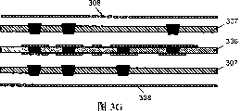
举例来说,如文献1中所揭示,以图3A到3I中所示的步骤来制造具有全层IVH结构的常规树脂多层布线板。For example, as disclosed in Document 1, a conventional resin multilayer wiring board having a full-layer IVH structure is manufactured in the steps shown in FIGS. 3A to 3I.
图3A中所示的电绝缘基板301是具有压缩特性的多孔基板、是具有在芯膜两侧上具有粘接层的三层结构的基板或由纤维和树脂制成的复合基板。覆盖膜302通过层压而被粘贴到电绝缘基板301的两侧上,如图3A所示。The electrically
接着,在图3B中,通过使用激光等来形成穿透所有电绝缘基板301和覆盖膜302的通孔303。Next, in FIG. 3B , a
在图3C中,使用导电膏304来填充通孔303。此时,覆盖膜防止导电膏残留在电绝缘基板上。In FIG. 3C , via
在图3D中,两侧上的覆盖膜302被剥除以暴露电绝缘基板301,且箔状布线材料305被层压在两侧上。In Fig. 3D, the
在图3E中,布线材料305通过加热和按压而被粘贴到电绝缘基板301上。电绝缘基板301具有压缩特性,从而通过加热和加压而在厚度方向上收缩电绝缘基板301。在此加热和按压步骤中,还可在厚度方向上压缩导电膏304。通过压缩使得导电膏中的金属填充物彼此高密度接触,从而布线材料305被电连接到导电膏304。此处,高密度接触状态是指许多金属填充物彼此接触且所述金属填充物的接触面积较大。In FIG. 3E, a
在图3F中,通过图案化布线材料305来完成双面布线板306。In FIG. 3F , double-sided
在图3G中,以与图3A到图3D所示步骤相同的步骤产生的填充有导电膏的电绝缘基板307被层压在双面布线板306的一个表面上。此时,通过辨认先前所形成的双面布线板306的布线图案的位置来定位电绝缘基板307。布线材料308被层压在电绝缘基板307的另一表面上。在电绝缘基板307中形成通孔时,基于双面布线板306的表面方向上的尺寸变化的测量结果来校正激光加工数据。In FIG. 3G , an electrically insulating
在图3H中,布线材料308通过加热和按压被粘贴到电绝缘基板307上。此时,双面布线板306同时被粘贴到电绝缘基板307上。在图3H的此加热和按压步骤中,在厚度方向上收缩电绝缘基板307,且也在厚度方向上压缩导电膏309,类似于图3E的步骤。通过压缩使得导电膏309与布线材料308和双面布线板上的布线310高密度接触,且因此实现电连接。In FIG. 3H, a
在图3I中,通过图案化表面上的布线材料308来完成多层布线板。此处,四层板被显示作为多层布线板;然而,多层布线板的层数目不限于四。可通过重复类似步骤来增加层数目。In FIG. 3I, the multilayer wiring board is completed by patterning the
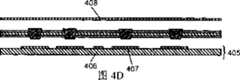
举例来说,在日本专利未审查公开No.2000-77800中揭示了另一常规实例。此文献揭示了一种结构,其中通过减小内部通孔的尺寸来实现高密度的层间连接且实现高可靠性。图4示出了此常规布线板的制造方法和结构特征。在图4中,简化了对与图3的步骤类似的步骤的描述。图4A到图4I是示出常规布线板的制造方法的主要步骤的截面图。For example, another conventional example is disclosed in Japanese Patent Unexamined Publication No. 2000-77800. This document discloses a structure in which high-density interlayer connections are realized and high reliability is achieved by reducing the size of internal via holes. FIG. 4 shows the manufacturing method and structural features of this conventional wiring board. In FIG. 4, descriptions of steps similar to those of FIG. 3 are simplified. 4A to 4I are sectional views showing main steps of a manufacturing method of a conventional wiring board.
在图4A中,在电绝缘基板401的两个表面上形成电绝缘粘接剂411,且在产品两侧上形成覆盖膜402。In FIG. 4A, an electrically insulating
在图4B中,形成穿透电绝缘基板401的通孔403。类似于常规实例,使用具有压缩特性的多孔基板、具有在芯膜两侧上形成粘接层的三层结构的基板或由纤维和树脂制成的复合基板作为电绝缘基板401。通过使用二氧化碳激光器、准分子激光器或YAG(钇铝石榴石)激光器进行激光加工来形成通孔。In FIG. 4B , a
在图4C中,使用导电膏404来填充通孔。In FIG. 4C ,
在图4D中,布线转移基板(或称为布线转印基板)405由支撑基板406和布线407形成,所述布线407以所要图案形成在所述支撑基板上。一般通过仅选择性蚀刻复合箔的铜箔来形成布线转移基板,其中所述铜箔以所要图案而层压在铝箔上。铜箔在铝箔上的形成通常通过电解电镀来执行,且铝与铜之间的应力极小。换句话说,其是以当通过蚀刻铜箔来形成布线图案时表面方向上的尺寸变化较小的方式构造的。In FIG. 4D , a wiring transfer substrate (or called a wiring transfer substrate) 405 is formed of a
接着,从电绝缘基板401的表面处剥除覆盖膜402。布线转移基板405被设置在电绝缘基板401的一个表面上,所述电绝缘基板401在其两个表面上均具有电绝缘粘接剂411,且布线材料408被设置在另一表面上,如图4D所示。Next, the
在图4A到图4D中,简单地首先描述电绝缘基板的形成步骤;然而,实际上,可首先形成布线转移基板405。在此情况下,在位置上辨认先前所形成的布线图案,响应于布线407的位置来校正激光加工数据,且可执行通孔加工。In FIGS. 4A to 4D , the forming step of the electrically insulating substrate is briefly described first; however, actually, the
接着,在图4E中,布线转移基板405、电绝缘基板401和布线材料408通过加热和按压而彼此粘贴。此时,布线转移基板405上的布线被埋入电绝缘基板401中。通过埋入布线407来有效地压缩被填充到通孔403中的导电膏404,使导电膏404中的金属填充物彼此高密度接触,导电膏404被电连接到布线407,且导电膏404被电连接到布线材料408。接着,在图4F中,通过蚀刻来图案化表面上的布线材料408以形成具有两层布线407的布线板409。Next, in FIG. 4E, the
接着,在图4G中,两层布线板409被定位和层压在填充有导电膏的电绝缘基板410的两侧上。此处,以与上述电绝缘基板401的制造方法类似的制造方法来制造电绝缘基板410。在每个附图中,简单地以相同布线图案来说明层压布线转移基板;然而,一般来说,使用不同的布线图案。Next, in FIG. 4G, two-layer wiring boards 409 are positioned and laminated on both sides of the electrically insulating substrate 410 filled with conductive paste. Here, the electrically insulating substrate 410 is manufactured in a manufacturing method similar to that of the above-described electrically
接着,在图4H中,电绝缘基板通过加热和按压而彼此粘贴。接着,在图4I中,将支撑基板406从表面处移除以完成多层布线板。此处,支撑基板406的移除方法取决于所采用的材料。当采用金属材料作为支撑基板406时,使用通过化学制品溶解的移除方法在生产率上是极佳的。当采用树脂片作为支撑基板时,一般机械地将它们剥除。Next, in FIG. 4H, the electrically insulating substrates are adhered to each other by heating and pressing. Next, in FIG. 4I, the
四层板被用作为所述多层布线板的实例;然而,多层布线板的层数目不限于四。可以类似步骤来增加层数目。在常规制造方法中,归因于电绝缘基板的压缩特性而在厚度方向上压缩导电膏,或通过将布线埋入电绝缘基板中来有效压缩导电膏。因此,导电膏中的金属填充物彼此高密度接触,且布线材料被电连接到导电膏。A four-layer board is used as an example of the multilayer wiring board; however, the number of layers of the multilayer wiring board is not limited to four. The number of layers can be increased in similar steps. In conventional manufacturing methods, the conductive paste is compressed in the thickness direction due to the compressive properties of the electrically insulating substrate, or is effectively compressed by embedding wiring in the electrically insulating substrate. Therefore, the metal fillers in the conductive paste are in high-density contact with each other, and the wiring material is electrically connected to the conductive paste.
然而,最近,已强烈需要使多层布线板变薄,且当采用薄电绝缘基板以满足此需求时,几乎不展示出压缩特性。因此,可观察到布线材料与导电膏之间的电连接电阻在高的一侧上变化的现象或在可靠性测试中通孔电阻稳定性恶化的现象。在不使用布线转移方法的一般制造方法中,当通过使用薄电绝缘基板来增加层数目时,不将布线埋入所述电绝缘基板之一的两个表面中。因此,不可期望通过将布线埋入电绝缘基板中来获得导电膏的压缩效果。Recently, however, there has been a strong demand for thinning multilayer wiring boards, and when a thin electrically insulating substrate is employed to meet this demand, little compressive properties are exhibited. Therefore, a phenomenon in which the electrical connection resistance between the wiring material and the conductive paste varies on the high side or a phenomenon in which the stability of the via resistance deteriorates in the reliability test can be observed. In a general manufacturing method that does not use a wiring transfer method, when the number of layers is increased by using a thin electrically insulating substrate, wiring is not buried in both surfaces of one of the electrically insulating substrates. Therefore, it is not expected to obtain the compressive effect of the conductive paste by embedding the wiring in the electrically insulating substrate.
换句话说,当通过使用薄电绝缘基板来制造具有全层IVH结构的多层布线板时,常规制造方法具有以下问题。一个问题是,难以有效地压缩导电膏,且因此布线材料与导电膏之间的电连接电阻在高的一侧上变化。另一个问题是,在可靠性测试中通孔电阻稳定性恶化。因此,难以使得具有全层IVH结构的多层布线板变薄。In other words, the conventional manufacturing method has the following problems when manufacturing a multilayer wiring board having a full-layer IVH structure by using a thin electrically insulating substrate. One problem is that it is difficult to effectively compress the conductive paste, and thus the electrical connection resistance between the wiring material and the conductive paste varies on the high side. Another problem is that via resistance stability deteriorates in reliability tests. Therefore, it is difficult to thin a multilayer wiring board having a full-layer IVH structure.
发明内容Contents of the invention
本发明提供一种多层布线板,所述多层布线板采用仅具有树脂流动作为压缩特性效果的薄绝缘基板。所述多层布线板具有全层IVH(内部通孔)结构,其中在不埋入布线的情况下形成至少一个绝缘基板。因此,可通过增加覆盖膜厚度与电绝缘基板厚度的比率来充分保证导体的碎裂(或压碎)容限。可有效地压缩填充到形成在薄绝缘基板中的通孔中的导体,其中在所述薄绝缘基板中几乎不能期望压缩特性效果。因此,可提供具有全层(或称为:所有层,任意层)IVH结构的薄多层布线板及其制造方法。The present invention provides a multilayer wiring board employing a thin insulating substrate having only resin flow as an effect of compression characteristics. The multilayer wiring board has a full-layer IVH (Inner Via Hole) structure in which at least one insulating substrate is formed without burying wiring. Therefore, the cracking (or crushing) tolerance of the conductor can be sufficiently secured by increasing the ratio of the cover film thickness to the thickness of the electrically insulating substrate. A conductor filled into a through-hole formed in a thin insulating substrate in which compressive characteristic effects can hardly be expected can be effectively compressed. Therefore, a thin multilayer wiring board having an all-layer (or called: all layers, arbitrary layers) IVH structure and a manufacturing method thereof can be provided.
附图说明Description of drawings
图1A是示出根据本发明示范性实施例1的多层布线板的制造方法的一步骤的截面图。1A is a sectional view showing a step of a method of manufacturing a multilayer wiring board according to Exemplary Embodiment 1 of the present invention.
图1B是示出根据示范性实施例1的多层布线板的制造方法的另一步骤的截面图。1B is a sectional view showing another step of the method of manufacturing the multilayer wiring board according to exemplary embodiment 1. FIG.
图1C是示出根据示范性实施例1的多层布线板的制造方法的又一步骤的截面图。1C is a sectional view showing still another step of the method of manufacturing the multilayer wiring board according to exemplary embodiment 1. FIG.
图1D是示出根据示范性实施例1的多层布线板的制造方法的又一步骤的截面图。1D is a sectional view showing still another step of the method of manufacturing the multilayer wiring board according to exemplary embodiment 1. FIG.
图1E是又根据示范性实施例1的多层布线板的制造方法的又一步骤的截面图。1E is a cross-sectional view of still another step of the method of manufacturing a multilayer wiring board according to yet another exemplary embodiment 1. FIG.
图1F是示出根据示范性实施例1的多层布线板的制造方法的又一步骤的截面图。1F is a cross-sectional view showing still another step of the method of manufacturing the multilayer wiring board according to exemplary embodiment 1. FIG.
图1G是示出根据示范性实施例1的多层布线板的制造方法的又一步骤的截面图。1G is a sectional view showing still another step of the method of manufacturing the multilayer wiring board according to exemplary embodiment 1. FIG.
图1H是又根据示范性实施例1的多层布线板的制造方法的又一步骤的截面图。1H is a cross-sectional view of still another step in the method of manufacturing a multilayer wiring board according to exemplary embodiment 1 again.
图1I是示出根据示范性实施例1的多层布线板的制造方法的又一步骤的截面图。FIG. 1I is a sectional view showing still another step of the method of manufacturing the multilayer wiring board according to exemplary embodiment 1. FIG.
图1J是示出根据示范性实施例1的多层布线板的制造方法的又一步骤的截面图。1J is a sectional view showing still another step of the method of manufacturing the multilayer wiring board according to exemplary embodiment 1. FIG.
图2A是展示根据本发明示范性实施例2的多层布线板的制造方法的一步骤的截面图。2A is a sectional view showing a step of a method of manufacturing a multilayer wiring board according to Exemplary Embodiment 2 of the present invention.
图2B是示出根据示范性实施例2的多层布线板的制造方法的又一步骤的截面图。2B is a sectional view showing still another step of the method of manufacturing the multilayer wiring board according to Exemplary Embodiment 2. FIG.
图2C是示出根据示范性实施例2的多层布线板的制造方法的又一步骤的截面图。2C is a sectional view showing still another step of the method of manufacturing the multilayer wiring board according to Exemplary Embodiment 2. FIG.
图2D是示出根据示范性实施例2的多层布线板的制造方法的又一步骤的截面图。2D is a sectional view showing still another step of the method of manufacturing the multilayer wiring board according to Exemplary Embodiment 2. FIG.
图2E是示出常规多层布线板的制造方法的一步骤的截面图。2E is a sectional view showing a step of a method of manufacturing a conventional multilayer wiring board.
图2F是示出根据示范性实施例2的多层布线板的制造方法的又一步骤的截面图。2F is a sectional view showing still another step of the method of manufacturing the multilayer wiring board according to Exemplary Embodiment 2. FIG.
图2G是示出根据示范性实施例2的多层布线板的制造方法的又一步骤的截面图。2G is a sectional view showing still another step of the method of manufacturing the multilayer wiring board according to Exemplary Embodiment 2. FIG.
图2H是示出根据示范性实施例2的多层布线板的制造方法的又一步骤的截面图。2H is a sectional view showing still another step of the method of manufacturing the multilayer wiring board according to Exemplary Embodiment 2. FIG.
图2I是示出根据示范性实施例2的多层布线板的制造方法的又一步骤的截面图。2I is a sectional view showing still another step of the method of manufacturing the multilayer wiring board according to Exemplary Embodiment 2. FIG.
图2J是示出根据示范性实施例2的多层布线板的制造方法的又一步骤的截面图。2J is a sectional view showing still another step of the method of manufacturing the multilayer wiring board according to Exemplary Embodiment 2. FIG.
图3A是示出常规多层布线板的制造方法的一步骤的截面图。3A is a cross-sectional view showing a step of a method of manufacturing a conventional multilayer wiring board.
图3B是示出常规多层布线板的制造方法的另一步骤的截面图。3B is a sectional view showing another step of the manufacturing method of the conventional multilayer wiring board.
图3C是示出常规多层布线板的制造方法的又一步骤的截面图。3C is a cross-sectional view showing still another step of the manufacturing method of the conventional multilayer wiring board.
图3D是示出常规多层布线板的制造方法的又一步骤的截面图。3D is a cross-sectional view showing still another step of the manufacturing method of the conventional multilayer wiring board.
图3E是示出常规多层布线板的制造方法的又一步骤的截面图。3E is a cross-sectional view showing still another step of the manufacturing method of the conventional multilayer wiring board.
图3F是示出常规多层布线板的制造方法的又一步骤的截面图。3F is a cross-sectional view showing still another step of the manufacturing method of the conventional multilayer wiring board.
图3G是示出常规多层布线板的制造方法的又一步骤的截面图。3G is a cross-sectional view showing still another step of the manufacturing method of the conventional multilayer wiring board.
图3H是示出常规多层布线板的制造方法的又一步骤的截面图。FIG. 3H is a sectional view showing still another step of the manufacturing method of the conventional multilayer wiring board.
图3I是示出常规多层布线板的制造方法的又一步骤的截面图。3I is a cross-sectional view showing still another step of the manufacturing method of the conventional multilayer wiring board.
图4A是示出另一常规多层布线板的制造方法的一步骤的截面图。4A is a cross-sectional view showing a step of another conventional multilayer wiring board manufacturing method.
图4B是示出所述常规多层布线板的制造方法的另一步骤的截面图。4B is a sectional view showing another step of the manufacturing method of the conventional multilayer wiring board.
图4C是示出所述常规多层布线板的制造方法的又步骤的截面图。FIG. 4C is a cross-sectional view showing further steps of the manufacturing method of the conventional multilayer wiring board.
图4D是示出所述常规多层布线板的制造方法的又一步骤的截面图。4D is a cross-sectional view showing still another step of the manufacturing method of the conventional multilayer wiring board.
图4E是示出所述常规多层布线板的制造方法的又一步骤的截面图。4E is a cross-sectional view showing still another step of the manufacturing method of the conventional multilayer wiring board.
图4F是示出所述常规多层布线板的制造方法的又一步骤的截面图。FIG. 4F is a sectional view showing still another step of the manufacturing method of the conventional multilayer wiring board.
图4G是示出所述常规多层布线板的制造方法的又一步骤的截面图。4G is a cross-sectional view showing still another step of the manufacturing method of the conventional multilayer wiring board.
图4H是示出所述常规多层布线板的制造方法的又一步骤的截面图。4H is a sectional view showing still another step of the manufacturing method of the conventional multilayer wiring board.
图4I是示出所述常规多层布线板的制造方法的又一步骤的截面图。FIG. 4I is a cross-sectional view showing still another step of the manufacturing method of the conventional multilayer wiring board.
附图标记reference sign
101 电绝缘基板101 Electrical insulating substrate
102 覆盖膜102 cover film
103 通孔103 through holes
104 导电膏104 conductive paste
105 铜箔105 copper foil
112 芯板112 core board
113 多层布线板113 multilayer wiring board
具体实施方式Detailed ways
(示范性实施例1)(Exemplary embodiment 1)
下文将参看附图来描述本发明的示范性实施例1。Exemplary Embodiment 1 of the present invention will be described below with reference to the drawings.
图1A到图1J是示出根据本发明示范性实施例1的多层布线板的制造方法的步骤的截面图。1A to 1J are cross-sectional views showing steps of a method of manufacturing a multilayer wiring board according to Exemplary Embodiment 1 of the present invention.
首先,在图1A中,覆盖膜102被粘贴到电绝缘基体材料(基板)101的两侧面上。First, in FIG. 1A , cover
电绝缘基板101具有在厚度方向上为5%或更低的基板可压缩性。使用由多孔基板和树脂制成的复合基板、仅由热固性树脂制成的基板、或由纤维和树脂制成的复合基板等作为电绝缘基板101。例如可使用通过用环氧树脂和氰酸酯树脂(cyanate resin)浸渍由延伸PTFE(聚四氟乙烯)形成的多孔膜而形成的复合基板作为由多孔基板和树脂制成的复合基板。单热固性树脂一般用环氧树脂涂覆。The electrically insulating
一般采用的具有80μm厚度的半固化片(prepreg:或称为预浸渍体)具有10%或更高的基板可压缩性。然而,当半固化片较薄时,厚度方向上的基板可压缩性易于降低。一般来说,为了提供具有压缩特性的绝缘基板,可以通过使半固化片呈多孔状态来增加多孔性,增加浸渍环氧树脂的树脂量,并且由此增加树脂流动特性。然而,当半固化片较薄时,仅树脂流动特性可预期作为压缩效果。举例来说,当半固化片的厚度小于40μm时,基板可压缩性低于5%。A generally used prepreg (prepreg: or prepreg) having a thickness of 80 μm has a compressibility of a substrate of 10% or more. However, when the prepreg is thin, the compressibility of the substrate in the thickness direction tends to decrease. In general, in order to provide an insulating substrate with compressive properties, it is possible to increase the porosity by making the prepreg porous, increase the amount of resin impregnated with the epoxy resin, and thereby increase the resin flow properties. However, when the prepreg is thinner, only resin flow characteristics can be expected as a compression effect. For example, when the thickness of the prepreg is less than 40 μm, the compressibility of the substrate is less than 5%.
在本实施例中,采用通过用环氧树脂浸渍包括芳族聚酰胺或玻璃纤维的无纺织物(无纺布)或纺织物而获得的复合基板。在本实施例中采用具有25到40μm的厚度的电绝缘基板。在此厚度中,即使当基板在真空热压步骤中被按压时基板也大体上仅通过树脂流动来在厚度方向上被压缩,且基板可压缩性低于5%。In this embodiment, a composite substrate obtained by impregnating a nonwoven fabric (nonwoven fabric) or a woven fabric including aramid or glass fiber with an epoxy resin is used. An electrically insulating substrate having a thickness of 25 to 40 μm is employed in the present embodiment. In this thickness, even when the substrate is pressed in the vacuum heat pressing step, the substrate is compressed in the thickness direction substantially only by resin flow, and the compressibility of the substrate is less than 5%.
关于常规导电膏,导体可压缩性必须为25%或更高以便保证通孔电阻稳定性。通过等式(1)来计算导体可压缩性。Regarding conventional conductive pastes, the conductor compressibility must be 25% or higher in order to ensure via resistance stability. Conductor compressibility is calculated by equation (1).
导体可压缩性=(导体的碎裂容限(crush-allowance)/导体填充高度)+基板可压缩性(等式1)Conductor compressibility = (crush-allowance of conductor/conductor fill height) + substrate compressibility (Equation 1)
举例来说,下面的结构能够保证使用通常采用的具有80μm厚度的半固化片时导体可压缩性为25%或更高。在此情况下,半固化片本身的厚度方向上的基板可压缩性为10%或更高。为了保证通孔电阻稳定性,覆盖膜的厚度设定为导体的碎裂容限为16μm或更大。换句话说,使用具有8μm或更大厚度的覆盖膜。因此,通过使用具有12到19μm的厚度的覆盖膜来制造具有全层IVH结构的一般多层布线板。For example, the following structure can ensure conductor compressibility of 25% or more using a commonly used prepreg having a thickness of 80 [mu]m. In this case, the substrate compressibility in the thickness direction of the prepreg itself is 10% or more. In order to ensure via-hole resistance stability, the thickness of the cover film is set so that the crack tolerance of the conductor is 16 μm or more. In other words, a cover film having a thickness of 8 μm or more is used. Therefore, a general multilayer wiring board having a full-layer IVH structure is manufactured by using a cover film having a thickness of 12 to 19 μm.
在本实施例中,覆盖膜102通过层压而粘贴到具有25到40μm的厚度的电绝缘基板101的两侧面上,如图1A所示。为了保证导体可压缩性为25%或更高,使用具有6到10μm的厚度的树脂膜(例如PET(聚对苯二甲酸乙二醇酯)或PEN(聚萘二甲酸乙二醇酯))作为覆盖膜。In the present embodiment, cover
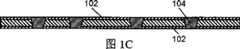
接着,在图1B中,通过激光加工或冲孔等来形成穿透所有电绝缘基板101和覆盖膜102的通孔103。当通孔103的壁表面倾斜时,更优选地采用激光加工。在激光加工的情况下,在电绝缘基板的前表面与后表面上的激光能量接收状态之间存在差异,从而能够通过改变激光条件来容易地控制穿透孔壁表面上的倾斜形状。Next, in FIG. 1B , a through
在图1C中,通过挤压使用导电膏104填充通孔103。使用含有金属填充物和树脂粘合剂的材料作为导电膏。金属填充物可由铜、银、金、锡、焊料或它们的合金制成。树脂粘合剂可由热固性树脂,例如环氧树脂或聚酰亚胺,制成。在本实施例中,通过使用铜作为金属填充物和使用环氧树脂作为树脂粘合剂来产生铜导电膏,且将其用作连接体。本发明的导电膏是在填入通孔103中时具有极好填充特性且适于保证碎裂容限以有效压缩层间传导的连接体。In FIG. 1C , via
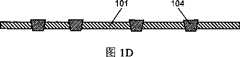
接着,在图1D中,将覆盖膜102从表面处剥除。在此状态中,导电膏104从电绝缘基板101的表面突起对应于覆盖膜102厚度的高度,且可保证较多导电膏。Next, in FIG. 1D , the
为了防止在剥除覆盖膜102时发生膏移除现象(paste-removingphenomenon),常规上,选择比电绝缘基板101充分薄的覆盖膜,且与激光孔直径相比,孔形状具有足够小的纵横比(aspect ratio)。此处,膏移除现象是指在剥除覆盖膜时导电膏104残留在形成于覆盖膜102中的孔中,且导电膏104的突起部分在剥除覆盖膜的同时被移除。In order to prevent the paste-removing phenomenon when peeling off the
由于以下原因而常规上使用此方法。即使当导电膏104的突起部分较小时,在真空热压步骤之后可有效地在厚度方向上压缩导电膏。这是因为电绝缘基板101具有压缩特性。因此,导电膏104中的金属填充物彼此高密度接触,且布线材料被电连接到导电膏104。This method is routinely used for the following reasons. Even when the protruding portion of the
当在真空热压步骤之后大体上仅通过树脂流动来在厚度方向上压缩电绝缘基板101时,依靠通过压缩而成的传统连接机制,难以有效地压缩导电膏104。因此,存在,布线材料与导电膏104之间的电连接电阻在较高一侧变化,或在可靠性测试中通孔电阻稳定性恶化等的问题。When the electrically insulating
在本实施例中,采用在其中几乎不能期望压缩特性效果的薄电绝缘基板101。为了有效地压缩填充到形成于薄电绝缘基板101中的通孔103中的导电膏104,导电膏104的碎裂容限必须足够大以在形成导电膏104且接着剥除覆盖膜102时获得有效的压缩。In the present embodiment, a thin electrically insulating
在本实施例中,使导电膏104的突起部分最大化解决了上述问题。为了使导电膏104的突起部分最大化,覆盖膜102与通孔103之间的纵横比必须增加到不发生膏移除现象的程度。实验展示在覆盖膜的厚度为通孔直径的20%或更小时不发生膏移除现象。In this embodiment, maximizing the protrusion portion of the
常规上,使用厚度为电绝缘基板厚度的约20%的覆盖膜。在本实施例中,必须使用更厚的覆盖膜102以便使导电膏104的突起部分最大化。过去的实验展示覆盖膜102的厚度必须为电绝缘基板厚度的约25%或更大以便以覆盖膜厚度来补偿常规电绝缘基板的压缩量。Conventionally, a cover film with a thickness of about 20% of the thickness of the electrically insulating substrate is used. In this embodiment, a
在本实施例中,使用满足式“覆盖膜厚度/通孔直径≤0.2”且具有为电绝缘基板厚度的约25%或更大的厚度的覆盖膜。举例来说,当将通过用环氧树脂来浸渍芳族聚酰胺无纺织物而形成的、具有35μm厚度的复合基板用作电绝缘基板时,使用具有9μm厚度的PEN膜来层压覆盖膜。此时,通孔103具有约80μm的直径,且是通过激光加工而形成的。In this embodiment, a cover film satisfying the expression "cover film thickness/via diameter≦0.2" and having a thickness of about 25% or more of the thickness of the electrically insulating substrate is used. For example, when a composite substrate having a thickness of 35 μm formed by impregnating an aramid nonwoven fabric with an epoxy resin is used as an electrical insulating substrate, a PEN film having a thickness of 9 μm is used to laminate the cover film. At this time, the via
接着,在图1E中,铜箔105被设置在图1D所示的电绝缘基板101的两个表面上,且铜箔105通过加热和按压而被粘贴到所述表面上,从而提供图1F所示的状态。在电绝缘基板101被完全粘贴到铜箔105的条件下执行此加热和按压步骤。举例来说,当电绝缘基板101含有热固性树脂时,此步骤在热固性树脂被完全固化的条件下执行。当导电膏104含有热固性树脂时,导电膏104中的树脂在此加热和按压步骤中也必须被固化。具体地说,当环氧树脂被用作为热固性树脂时,环氧树脂可在50kgf/cm2、200℃和一个小时的加热和按压条件下被固化。Next, in FIG. 1E ,
在加热和按压步骤中,重要的是使导电膏104中所含的金属填充物彼此高密度接触以便使与通孔103的电连接稳定。优选地,电绝缘基板101具有以下特性。当电绝缘基板101中所含的热固性树脂在加热和按压步骤中固化和粘贴之前被暂时液化且流动时,可保持穿透孔形状的壁从而金属填充物不被同时带走。In the heating and pressing step, it is important to bring the metal fillers contained in the
因此,优选地采用通过用树脂浸渍由PTFE形成的多孔片而形成的基板、或通过用树脂浸渍由芳族聚酰胺或玻璃纤维制成的无纺织物或纺织物而形成的基板作为电绝缘基板101。采用此基板实现更高密度的接触,因为在加热和按压步骤中金属填充物在厚度方向上被压缩而不在电绝缘基板101的表面方向上流动。优选地,使导电膏104的突起部分尽可能地大,以便实现高密度接触。这是因为金属填充物在厚度方向上可被进一步压缩。可使用通过以含有例如硅石或氧化铝等的无机填充物的树脂组合物来浸渍片而形成的电绝缘基板101。当使用此类树脂组合物时,电绝缘基板101具有脆性。因此,难以在所述步骤中保持本身形状,但可降低电绝缘基板101在厚度方向上的热膨胀,且因此可增加通孔中电连接的可靠性。Therefore, a substrate formed by impregnating a porous sheet formed of PTFE with a resin, or a substrate formed by impregnating a non-woven fabric or a woven fabric made of aramid or glass fiber with a resin is preferably used as the electrically insulating
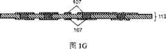
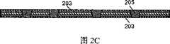
接着,在图1G中,通过图案化铜箔105来完成具有布线107的芯板112。Next, in FIG. 1G , the
通过将覆盖膜粘贴到未固化的电绝缘基板101的两个表面上、形成通孔、接着在通孔中形成导体、剥除覆盖膜、在两个表面上粘贴并图案化铜箔105来形成芯板112。在芯板112中,导体的一部分在剥除覆盖膜之后从电绝缘基板的表面处突起,且因此可保证导体的碎裂容限。因此,即使当限定布线的铜箔105被形成而不被埋入芯板112中时,也可充分压缩导体。Formed by sticking a cover film to both surfaces of an uncured electrically insulating
在图1H中,电绝缘基板111a和111b与芯板112的两个表面对准,使得它们与形成在芯板112上的布线图案的所要位置匹配,且铜箔105被层压在外部的两个表面上。通过使用真空热压来加热并按压所述层压产品,从而提供图1I所示的层压体。以与图1A到图1D中的步骤类似的步骤来产生电绝缘基板111a和111b。In FIG. 1H, the electrically insulating
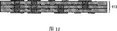
在图1J中,通过图案化层压体表面上的铜箔105来完成多层布线板113。In FIG. 1J, a
如上论述,本实施例的多层布线板113采用仅具有树脂流动作为压缩效果的薄电绝缘基板,但可通过增加覆盖膜厚度与电绝缘基板厚度的比率来充分保证导体的碎裂容限。因此,即使当布线图案被形成而不埋入电绝缘基板中时,也可在厚度方向上压缩金属填充物。因此,可实现高密度接触,且可增加通孔中的电连接的可靠性。可获得具有全层IVH结构的极薄多层布线板作为多层布线板。As discussed above, the
图1J中所示的四层布线板被形成为本实施例中的多层布线板;然而,可通过重复图1H所示的层压来增加层数目。层数目不限于四(图1),且可以类似步骤来进一步增加数目。The four-layer wiring board shown in FIG. 1J is formed as a multilayer wiring board in this embodiment; however, the number of layers can be increased by repeating the lamination shown in FIG. 1H. The number of layers is not limited to four (FIG. 1), and the number can be further increased in similar steps.
(示范性实施例2)(Exemplary embodiment 2)
下文将参看附图来描述本发明的示范性实施例2。Exemplary Embodiment 2 of the present invention will be described below with reference to the drawings.
图2A到图2J是展示根据本发明示范性实施例2的多层布线板的制造方法的步骤的截面图。简化了对与实施例1中的元件类似的元件的描述。2A to 2J are cross-sectional views showing steps of a method of manufacturing a multilayer wiring board according to Exemplary Embodiment 2 of the present invention. Descriptions of elements similar to those in Embodiment 1 are simplified.
首先,在图2A中,电绝缘粘接剂202被涂覆到电绝缘基板201的两个表面上,且覆盖膜203被进一步粘贴到产品的两侧面上。First, in FIG. 2A, an electrically insulating
图2A的电绝缘基板201具有在厚度方向上为5%或更低的基板可压缩性。本实施例的电绝缘基板201由耐热膜材料制成。为了在印刷布线板中使用所述膜材料,优选地,所述膜材料即使在被加热到回流温度(reflowtemperature),即约280℃时,也不会溶解或软化。在加热之后尺寸变化较小的材料是更优选的。举例来说,可使用聚酰亚胺膜或芳族聚酰胺膜等作为此类膜材料。The electrically insulating
在本实施例中,具有12.5μm的厚度的聚酰亚胺膜被用作为电绝缘基板201。电绝缘粘接剂202被施加到电绝缘基板201的两个表面上。优选地,使用例如环氧树脂或环氧改性聚酰亚胺树脂(epoxy modified polyimideresin)等的热固粘接剂作为电绝缘粘接剂202。在本实施例中,具有170℃的固化温度的热固环氧粘接剂以5到10μm的厚度被应用。覆盖膜203通过层压而被粘贴到电绝缘粘接剂202的两侧上。使用由PET、PEN等制成的树脂膜作为覆盖膜203,且其厚度可设定为6到10μm。在本实施例中使用具有9μm厚度的PEN膜。In this embodiment, a polyimide film having a thickness of 12.5 μm was used as the electrically insulating
实施例2中所使用的膜基板可提供比实施例1中所述的采用半固化片的基板更薄的电绝缘基板。但是,在实施例2的制造步骤中所执行的真空热压步骤中膜材料未被压缩。因此,仅施加到两个表面上的未固化热固性粘接剂流动并固化,使得整个膜基板的压缩量变得极小。然而,膜材料可被应用作为本发明全层IVH结构的多层布线板的材料。The film substrate used in Example 2 can provide a thinner electrically insulating substrate than the substrate described in Example 1 using a prepreg. However, the film material was not compressed in the vacuum heat pressing step performed in the manufacturing step of Example 2. Therefore, only the uncured thermosetting adhesive applied to the two surfaces flows and cures, so that the amount of compression of the entire film substrate becomes extremely small. However, film materials can be applied as the material of the multilayer wiring board of the full-layer IVH structure of the present invention.
在图2A之后,当执行与实施例1的步骤类似的步骤(如图2B到图2D所示)时,导电膏205从电绝缘基板201的表面处突起对应于覆盖膜203厚度的高度。After FIG. 2A , when steps similar to those of Embodiment 1 are performed (as shown in FIGS. 2B to 2D ), the
在实施例2中,使用在真空热压步骤之后大体上仅通过树脂流动来在厚度方向上被压缩的电绝缘基板201。因此,依靠压缩而成的常规连接机制,难以有效地压缩导电膏205。因此,存在,布线材料与导电膏205之间的电连接电阻在较高一侧变化,或在可靠性测试中通孔电阻稳定性恶化等的问题。In Example 2, the electrically insulating
同样在本实施例中,为了使得导电膏205的突起部分最大化,形成于覆盖膜203中的通孔204的纵横比被增加到不发生膏移除现象的程度。在本实施例中还已知,当覆盖膜厚度/通孔直径≤0.2时,不发生膏移除现象。Also in this embodiment, in order to maximize the protruding portion of the
常规上,使用厚度为电绝缘基板厚度的约20%的覆盖膜203。在实施例2中,必须使用较厚的覆盖膜203以便使导电膏205的突起部分最大化。覆盖膜203的厚度必须为电绝缘基板厚度的约25%或更大,以便以覆盖膜厚度来补偿常规电绝缘基板的压缩量,如实施例1所示。Conventionally, a
在本实施例中,环氧粘接剂以5到10μm的厚度被涂覆到作为电绝缘基板的12.5μm厚的聚酰亚胺膜的两个表面上。使用具有22.5到32.5μm总厚度的复合基板,将具有9μm厚度的PEN膜层压到覆盖膜203上。具有约50到80μm的直径的通孔204通过激光加工而形成在所述层压体中(图2B)。In this embodiment, an epoxy adhesive was applied in a thickness of 5 to 10 μm on both surfaces of a 12.5 μm thick polyimide film as an electrically insulating substrate. A PEN film having a thickness of 9 μm was laminated onto the
在图2C中,使用导电膏205来填充通孔204。接着,剥除覆盖膜203以形成具有导电膏205的突起部分的层压体,如图2D所示。In FIG. 2C , via
接着,在图2E中,铜箔206被设置在图2D所示的电绝缘基板201的两个表面上,且铜箔206通过加热和按压而被粘贴到所述表面上,从而提供图2F所示的状态。在电绝缘粘接剂202完全粘贴到铜箔206的条件下执行图2F的此加热和按压步骤。举例来说,当电绝缘粘接剂含有热固性树脂时,此步骤在热固性树脂被完全固化的条件下执行。当导电膏205含有热固性树脂时,导电膏中的树脂在此加热和按压步骤中也必须被固化。具体地说,当环氧树脂被用作热固性树脂时,环氧树脂可在50kgf/cm2、200℃和一个小时的加热和按压条件下被固化。Next, in FIG. 2E ,
在加热和按压步骤中,重要的是使得导电膏205中所含的金属填充物彼此高密度接触以便使与通孔的电连接稳定。当电绝缘基板201中所含的热固性树脂在加热和按压步骤中固化和粘贴之前被暂时液化且流动时,必须保持穿透孔形状的壁,从而不同时带走金属填充物。因此,最优选地采用聚酰亚胺膜作为电绝缘基板201。在加热和按压步骤中金属填充物由于聚酰亚胺膜的壁效应而在厚度方向上被压缩而不在电绝缘基板201的表面方向上流动,从而实现较高密度接触。优选地,使导电膏205的突起部分尽可能地大以便实现高密度接触。这是因为在此情况下金属填充物在厚度方向上被进一步压缩。In the heating and pressing steps, it is important to bring the metal fillers contained in the
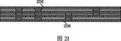
接着,在图2G中,通过图案化铜箔206来完成具有布线207的芯板212。Next, in FIG. 2G , the
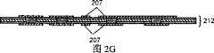
在图2H中,电绝缘基板211a和212b与芯板212的两个表面对准,使得它们与形成在芯板212上的布线图案的所要位置匹配,且进一步铜箔206被设置在外部的两个表面上。通过使用真空热压来加热并按压所述层压产品,从而提供图2I所示的层压体。在与图2A到图2D的步骤类似的步骤中预先产生电绝缘基板211a和211b。In FIG. 2H, the electrically insulating
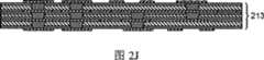
在图2J中,通过图案化层压体表面上的铜箔206来完成多层布线板213。In FIG. 2J, the
以此方法制造的多层布线板213采用通过将电绝缘粘接剂202施加到膜状电绝缘基板201上而形成的复合基板,所述电绝缘基板201仅具有树脂流动作为压缩效果。然而,可通过增加覆盖膜203厚度与整个电绝缘基板厚度的比率来充分保证导体的碎裂容限。由于保证了导体的碎裂容限,因而即使当布线207被形成而被不埋入电绝缘基板中时也可在厚度方向上压缩金属填充物。因此,可实现高密度接触,且可改进通孔中电连接的可靠性。可获得具有全层IVH结构的极薄多层布线板作为多层布线板。The
图2J中所示的四层布线板被形成为本实施例中的多层布线板;然而,可通过重复图2H所示的层压来进一步增加层数目。图2A到图2J展示一个实例,层数目不限于四,且可通过重复类似步骤来进一步增加数目。The four-layer wiring board shown in FIG. 2J is formed as a multilayer wiring board in this embodiment; however, the number of layers can be further increased by repeating the lamination shown in FIG. 2H. Figures 2A-2J show one example, the number of layers is not limited to four, and the number can be further increased by repeating similar steps.
在本发明中,可通过增加对电绝缘基板厚度的覆盖膜厚度的比率来充分保证导体的碎裂容限。因此,可有效地压缩导体,且可保证通孔电阻稳定性。即使当仅具有树脂流动作为压缩效果的薄电绝缘基板被用作为电绝缘基板时,也可在不埋入布线的情况下在芯层中形成通孔。因此,可形成在两个表面中均不具有埋入的布线的芯板,且可有利地形成采用电绝缘基板的具有全层IVH结构的多层布线板,其中所有层均为薄的。In the present invention, the crack tolerance of the conductor can be sufficiently secured by increasing the ratio of the thickness of the cover film to the thickness of the electrically insulating substrate. Therefore, the conductor can be effectively compressed, and via hole resistance stability can be ensured. Even when a thin electrically insulating substrate having only resin flow as a compressive effect is used as the electrically insulating substrate, via holes can be formed in the core layer without burying wiring. Therefore, a core board having no buried wiring in both surfaces can be formed, and a multilayer wiring board having a full-layer IVH structure using an electrically insulating substrate in which all layers are thin can be advantageously formed.
工业适用性Industrial applicability
采用电绝缘基板的、具有全层IVH结构的多层布线板,其中所有层均为薄的,可以极小厚度来实现高密度组件可安装性和布线可存储性。归因于所述小厚度,还可容易地提供某种程度的可弯曲性,使得可通过在设备的壳体中使用间隙来有效安装所述板。因此,此布线板对于需要小厚度、轻重量和高功能的电子设备,尤其对于便携式电子设备极为有用。A multilayer wiring board with a full-layer IVH structure using an electrically insulating substrate, in which all layers are thin, can achieve high-density component mountability and wiring storability with extremely small thickness. Due to the small thickness it is also easy to provide a certain degree of bendability so that the plate can be efficiently mounted by using clearances in the housing of the device. Therefore, this wiring board is extremely useful for electronic equipment requiring small thickness, light weight, and high functionality, especially portable electronic equipment.
Claims (10)
Applications Claiming Priority (2)
| Application Number | Priority Date | Filing Date | Title |
|---|---|---|---|
| JP131964/2005 | 2005-04-28 | ||
| JP2005131964 | 2005-04-28 |
Publications (2)
| Publication Number | Publication Date |
|---|---|
| CN101032194Atrue CN101032194A (en) | 2007-09-05 |
| CN100558222C CN100558222C (en) | 2009-11-04 |
Family
ID=37307940
Family Applications (1)
| Application Number | Title | Priority Date | Filing Date |
|---|---|---|---|
| CN200680000919.4AExpired - Fee RelatedCN100558222C (en) | 2005-04-28 | 2006-04-26 | Multilayer wiring board and manufacturing method thereof |
Country Status (5)
| Country | Link |
|---|---|
| US (1) | US8076589B2 (en) |
| JP (1) | JPWO2006118141A1 (en) |
| CN (1) | CN100558222C (en) |
| TW (1) | TW200704298A (en) |
| WO (1) | WO2006118141A1 (en) |
Cited By (4)
| Publication number | Priority date | Publication date | Assignee | Title |
|---|---|---|---|---|
| CN101835343A (en)* | 2009-03-09 | 2010-09-15 | 株式会社电装 | Printed wiring board, the printed IC board that comprises it and manufacture method thereof |
| CN102939803A (en)* | 2010-06-08 | 2013-02-20 | 松下电器产业株式会社 | Multilayer wiring substrate and method for manufacturing multilayer wiring substrate |
| CN106735922A (en)* | 2017-01-16 | 2017-05-31 | 深圳顺络电子股份有限公司 | A kind of laminate electronic components and preparation method thereof |
| CN112335179A (en)* | 2018-07-30 | 2021-02-05 | 京瓷株式会社 | Composite substrate |
Families Citing this family (5)
| Publication number | Priority date | Publication date | Assignee | Title |
|---|---|---|---|---|
| JP2008244325A (en)* | 2007-03-28 | 2008-10-09 | Japan Gore Tex Inc | Printed wiring boards and ball grid array packages |
| JP5587139B2 (en)* | 2010-11-04 | 2014-09-10 | 日本特殊陶業株式会社 | Multilayer wiring board |
| JP5881173B2 (en)* | 2012-10-31 | 2016-03-09 | 京セラサーキットソリューションズ株式会社 | Wiring board manufacturing method |
| CN113473748A (en)* | 2020-03-30 | 2021-10-01 | 健鼎(湖北)电子有限公司 | Manufacturing method of multilayer connecting plate |
| US12342470B2 (en) | 2022-08-08 | 2025-06-24 | Reophotonics, Ltd. | Methods to fill through-holes of a substrate with metal paste |
Family Cites Families (8)
| Publication number | Priority date | Publication date | Assignee | Title |
|---|---|---|---|---|
| JP2991032B2 (en) | 1994-04-15 | 1999-12-20 | 松下電器産業株式会社 | Method for manufacturing multilayer substrate |
| JP2921400B2 (en)* | 1994-06-24 | 1999-07-19 | 松下電器産業株式会社 | Multilayer printed wiring board and method of manufacturing the same |
| JP3889856B2 (en)* | 1997-06-30 | 2007-03-07 | 松下電器産業株式会社 | Method for manufacturing printed wiring board with protruding electrodes |
| TW410534B (en)* | 1997-07-16 | 2000-11-01 | Matsushita Electric Industrial Co Ltd | Wiring board and production process for the same |
| JPH11298105A (en)* | 1998-04-07 | 1999-10-29 | Asahi Chem Ind Co Ltd | Via hole filling type printed board and manufacture thereof |
| JP3215090B2 (en) | 1998-06-16 | 2001-10-02 | 松下電器産業株式会社 | Wiring board, multilayer wiring board, and methods of manufacturing the same |
| JP2002064270A (en)* | 2000-08-17 | 2002-02-28 | Matsushita Electric Ind Co Ltd | Circuit board and its manufacturing method |
| TW545092B (en)* | 2001-10-25 | 2003-08-01 | Matsushita Electric Industrial Co Ltd | Prepreg and circuit board and method for manufacturing the same |
- 2006
- 2006-04-26CNCN200680000919.4Apatent/CN100558222C/ennot_activeExpired - Fee Related
- 2006-04-26JPJP2006526471Apatent/JPWO2006118141A1/enactivePending
- 2006-04-26USUS11/629,311patent/US8076589B2/ennot_activeExpired - Fee Related
- 2006-04-26TWTW095114938Apatent/TW200704298A/enunknown
- 2006-04-26WOPCT/JP2006/308724patent/WO2006118141A1/ennot_activeCeased
Cited By (4)
| Publication number | Priority date | Publication date | Assignee | Title |
|---|---|---|---|---|
| CN101835343A (en)* | 2009-03-09 | 2010-09-15 | 株式会社电装 | Printed wiring board, the printed IC board that comprises it and manufacture method thereof |
| CN102939803A (en)* | 2010-06-08 | 2013-02-20 | 松下电器产业株式会社 | Multilayer wiring substrate and method for manufacturing multilayer wiring substrate |
| CN106735922A (en)* | 2017-01-16 | 2017-05-31 | 深圳顺络电子股份有限公司 | A kind of laminate electronic components and preparation method thereof |
| CN112335179A (en)* | 2018-07-30 | 2021-02-05 | 京瓷株式会社 | Composite substrate |
Also Published As
| Publication number | Publication date |
|---|---|
| TW200704298A (en) | 2007-01-16 |
| WO2006118141A1 (en) | 2006-11-09 |
| US20080308304A1 (en) | 2008-12-18 |
| CN100558222C (en) | 2009-11-04 |
| JPWO2006118141A1 (en) | 2008-12-18 |
| US8076589B2 (en) | 2011-12-13 |
Similar Documents
| Publication | Publication Date | Title |
|---|---|---|
| CN1189068C (en) | Multilayer printed circuit board and manufacturing method thereof | |
| CN1204786C (en) | Circuit board and manufacturing method thereof | |
| CN1201642C (en) | Printed circuit board and manufacturing method thereof | |
| CN1282404C (en) | Method for manufacturing double-sided circuit board for lamination and multilayer printed circuit board using the same | |
| CN1180666C (en) | Printed wiring board and method of manufacturing printed wiring board | |
| CN1056490C (en) | Method for manufacturing printed circuit board and substrate manufactured by the method | |
| CN101032194A (en) | Multilayer wiring board and manufacturing method thereof | |
| CN1197441C (en) | Printed wiring board and its manufacturing method | |
| CN100345279C (en) | Component built-in module and method of manufacturing the same | |
| CN1101126C (en) | Wiring board and its producing method | |
| CN1264388C (en) | Resin board and use thereof | |
| CN1236658C (en) | Monolithic ceramic electronic element and its producing method and electronic device | |
| CN1577819A (en) | Circuit board with in-built electronic component and method for manufacturing the same | |
| CN1106188A (en) | Printed circuit board and method of manufacturing the same | |
| CN1610491A (en) | Parallel multi-layer printed circuit board having improved interconnection and method for manufacturing the same | |
| CN1835654A (en) | Wiring board and method of manufacturing the same | |
| CN1929721A (en) | Method for forming wiring on insulating resin layer | |
| CN1671268A (en) | Flexible substrate, multilayer flexible substrate, and their manufacturing methods | |
| CN1343089A (en) | Printed circuit board with channel and manufacturing method thereof | |
| CN1242657C (en) | Improved bonding strength between conductive paste and printed substrate and its production method | |
| CN1826037A (en) | Rigid-flex printed circuit board and manufacturing method thereof | |
| CN1212049C (en) | Circuit-formed substrate and method for manufacturing circuit-formed substrate | |
| CN1525804A (en) | Circuit board and manufacturing method thereof | |
| CN1182764C (en) | Manufacturing method of ceramic substrate | |
| CN1551709A (en) | A circuit board component, a method for manufacturing the component, and a method for manufacturing a circuit board |
Legal Events
| Date | Code | Title | Description |
|---|---|---|---|
| C06 | Publication | ||
| PB01 | Publication | ||
| C10 | Entry into substantive examination | ||
| SE01 | Entry into force of request for substantive examination | ||
| C14 | Grant of patent or utility model | ||
| GR01 | Patent grant | ||
| C17 | Cessation of patent right | ||
| CF01 | Termination of patent right due to non-payment of annual fee | Granted publication date:20091104 Termination date:20140426 |