CN101030602B - MOS transistor for decreasing short channel and its production - Google Patents
MOS transistor for decreasing short channel and its productionDownload PDFInfo
- Publication number
- CN101030602B CN101030602BCN2007100391861ACN200710039186ACN101030602BCN 101030602 BCN101030602 BCN 101030602BCN 2007100391861 ACN2007100391861 ACN 2007100391861ACN 200710039186 ACN200710039186 ACN 200710039186ACN 101030602 BCN101030602 BCN 101030602B
- Authority
- CN
- China
- Prior art keywords
- mos transistor
- groove
- short channel
- grid
- drain
- Prior art date
- Legal status (The legal status is an assumption and is not a legal conclusion. Google has not performed a legal analysis and makes no representation as to the accuracy of the status listed.)
- Active
Links
- 238000004519manufacturing processMethods0.000titleclaimsabstractdescription27
- 230000003247decreasing effectEffects0.000titleclaims11
- 238000000034methodMethods0.000claimsabstractdescription26
- 229910052710siliconInorganic materials0.000claimsabstractdescription26
- 239000010703siliconSubstances0.000claimsabstractdescription26
- XUIMIQQOPSSXEZ-UHFFFAOYSA-NSiliconChemical compound[Si]XUIMIQQOPSSXEZ-UHFFFAOYSA-N0.000claimsabstractdescription24
- 229910021332silicideInorganic materials0.000claimsabstractdescription8
- FVBUAEGBCNSCDD-UHFFFAOYSA-Nsilicide(4-)Chemical compound[Si-4]FVBUAEGBCNSCDD-UHFFFAOYSA-N0.000claimsabstractdescription8
- 239000000758substrateSubstances0.000claimsdescription24
- 239000002184metalSubstances0.000claimsdescription9
- 229920002120photoresistant polymerPolymers0.000claimsdescription8
- 238000001039wet etchingMethods0.000claimsdescription5
- 230000003647oxidationEffects0.000claimsdescription3
- 238000007254oxidation reactionMethods0.000claimsdescription3
- 238000002347injectionMethods0.000claims5
- 239000007924injectionSubstances0.000claims5
- 208000002173dizzinessDiseases0.000claims2
- 239000012212insulatorSubstances0.000claims2
- 150000003376siliconChemical class0.000claims2
- 238000005260corrosionMethods0.000claims1
- 230000007797corrosionEffects0.000claims1
- 238000001459lithographyMethods0.000claims1
- 230000000694effectsEffects0.000abstractdescription35
- 238000002955isolationMethods0.000abstractdescription6
- 230000015556catabolic processEffects0.000abstractdescription2
- 239000010410layerSubstances0.000description24
- 238000002513implantationMethods0.000description16
- 125000001475halogen functional groupChemical group0.000description7
- 125000006850spacer groupChemical group0.000description4
- 238000005530etchingMethods0.000description3
- VYPSYNLAJGMNEJ-UHFFFAOYSA-NSilicium dioxideChemical compoundO=[Si]=OVYPSYNLAJGMNEJ-UHFFFAOYSA-N0.000description2
- 238000005137deposition processMethods0.000description2
- 239000011229interlayerSubstances0.000description2
- 238000000206photolithographyMethods0.000description2
- 239000004065semiconductorSubstances0.000description2
- 229910052814silicon oxideInorganic materials0.000description2
- 230000007547defectEffects0.000description1
- 238000000407epitaxyMethods0.000description1
- 238000009413insulationMethods0.000description1
- 229910021420polycrystalline siliconInorganic materials0.000description1
- 229920005591polysiliconPolymers0.000description1
- 238000004080punchingMethods0.000description1
Images


Classifications
- H—ELECTRICITY
- H10—SEMICONDUCTOR DEVICES; ELECTRIC SOLID-STATE DEVICES NOT OTHERWISE PROVIDED FOR
- H10D—INORGANIC ELECTRIC SEMICONDUCTOR DEVICES
- H10D30/00—Field-effect transistors [FET]
- H10D30/60—Insulated-gate field-effect transistors [IGFET]
- H10D30/601—Insulated-gate field-effect transistors [IGFET] having lightly-doped drain or source extensions, e.g. LDD IGFETs or DDD IGFETs
- H10D30/608—Insulated-gate field-effect transistors [IGFET] having lightly-doped drain or source extensions, e.g. LDD IGFETs or DDD IGFETs having non-planar bodies, e.g. having recessed gate electrodes
- H—ELECTRICITY
- H10—SEMICONDUCTOR DEVICES; ELECTRIC SOLID-STATE DEVICES NOT OTHERWISE PROVIDED FOR
- H10D—INORGANIC ELECTRIC SEMICONDUCTOR DEVICES
- H10D62/00—Semiconductor bodies, or regions thereof, of devices having potential barriers
- H10D62/10—Shapes, relative sizes or dispositions of the regions of the semiconductor bodies; Shapes of the semiconductor bodies
- H10D62/17—Semiconductor regions connected to electrodes not carrying current to be rectified, amplified or switched, e.g. channel regions
- H10D62/351—Substrate regions of field-effect devices
- H10D62/357—Substrate regions of field-effect devices of FETs
- H10D62/364—Substrate regions of field-effect devices of FETs of IGFETs
- H10D62/371—Inactive supplementary semiconductor regions, e.g. for preventing punch-through, improving capacity effect or leakage current
- H—ELECTRICITY
- H10—SEMICONDUCTOR DEVICES; ELECTRIC SOLID-STATE DEVICES NOT OTHERWISE PROVIDED FOR
- H10D—INORGANIC ELECTRIC SEMICONDUCTOR DEVICES
- H10D64/00—Electrodes of devices having potential barriers
- H10D64/01—Manufacture or treatment
- H10D64/025—Manufacture or treatment forming recessed gates, e.g. by using local oxidation
- H10D64/027—Manufacture or treatment forming recessed gates, e.g. by using local oxidation by etching at gate locations
- H—ELECTRICITY
- H10—SEMICONDUCTOR DEVICES; ELECTRIC SOLID-STATE DEVICES NOT OTHERWISE PROVIDED FOR
- H10D—INORGANIC ELECTRIC SEMICONDUCTOR DEVICES
- H10D30/00—Field-effect transistors [FET]
- H10D30/01—Manufacture or treatment
- H10D30/021—Manufacture or treatment of FETs having insulated gates [IGFET]
- H10D30/0212—Manufacture or treatment of FETs having insulated gates [IGFET] using self-aligned silicidation
Landscapes
- Insulated Gate Type Field-Effect Transistor (AREA)
Abstract
Description
Translated fromChinese技术领域technical field
本发明涉及半导体制造领域,特别涉及一种可减小短沟道效应的MOS晶体管及其制作方法。The invention relates to the field of semiconductor manufacturing, in particular to a MOS transistor capable of reducing short-channel effects and a manufacturing method thereof.
背景技术Background technique
半导体器件通过按比例缩小来实现工作速度的提升。MOS晶体管的沟道长度也在不断的按比例缩短,但当MOS晶体管的沟道长度变得非常短时,短沟道效应会使器件性能劣化,甚至无法正常工作。减小栅极绝缘层的厚度或制作浅结的源极和漏极均可有效的减小短沟道效应,但现在栅极绝缘层的厚度已达到极限,当再减小时易导致栅极的漏电流增大或栅极的击穿,故无法通过减小栅极绝缘层的厚度来减小短沟道效应;另外为确保栅、漏极的较小的接触电阻,故需确保栅、漏极表面具一定厚度的金属硅化物层,故也很难通过制作浅结的源极和漏极来减小短沟道效应。Semiconductor devices achieve increased operating speeds by scaling down. The channel length of the MOS transistor is also continuously shortened in proportion, but when the channel length of the MOS transistor becomes very short, the short channel effect will degrade the performance of the device, or even fail to work normally. Reducing the thickness of the gate insulating layer or making the source and drain of the shallow junction can effectively reduce the short channel effect, but now the thickness of the gate insulating layer has reached the limit, and when it is further reduced, it will easily lead to the short channel effect. Leakage current increases or gate breakdown, so the short channel effect cannot be reduced by reducing the thickness of the gate insulating layer; in addition, in order to ensure the small contact resistance of the gate and drain, it is necessary to ensure The pole surface has a metal silicide layer with a certain thickness, so it is also difficult to reduce the short channel effect by making shallow junction source and drain electrodes.
为减小上述短沟道效应,现通常使用外延工艺制作抬高的源极和漏极。但是外延工艺是一种成本很高、难于控制的工艺技术,存在高复杂性、高成本、高缺陷密度等问题。In order to reduce the above-mentioned short-channel effect, the raised source and drain are usually fabricated by epitaxial process. However, the epitaxy process is a high-cost and difficult-to-control process technology, which has problems such as high complexity, high cost, and high defect density.
发明内容Contents of the invention
本发明的目的在于提供一种可减小短沟道效应的MOS晶体管及其制作方法,通过所述MOS晶体管及其制作方法可有效的减小短沟道效应,并可降低工艺难度和制作成本。The object of the present invention is to provide a MOS transistor capable of reducing the short-channel effect and its manufacturing method, through which the short-channel effect can be effectively reduced, and the process difficulty and manufacturing cost can be reduced .
本发明的目的是这样实现的:一种可减小短沟道效应的MOS晶体管,该MOS晶体管制作在已制成场隔离区的硅衬底上,该MOS晶体管包括栅极堆层、栅极侧墙、源极以及漏极,其中,该栅极堆层包括依次层叠的栅极绝缘层与栅极,该源极和漏极顶部具有金属硅化物层,其中,该硅衬底上制作有凹槽,该栅极堆层设置在该凹槽中。The object of the present invention is achieved like this: a kind of MOS transistor that can reduce the short channel effect, and this MOS transistor is made on the silicon substrate that has made field isolation region, and this MOS transistor comprises gate stack layer, gate sidewall, source and drain, wherein the gate stack layer includes a gate insulating layer and a gate stacked in sequence, the top of the source and drain has a metal silicide layer, wherein the silicon substrate is fabricated A groove, the gate stack layer is disposed in the groove.
在上述的可减小短沟道效应的MOS晶体管中,该凹槽的面积不小于该栅极堆层的面积。In the above-mentioned MOS transistor capable of reducing the short channel effect, the area of the groove is not smaller than the area of the gate stack.
在上述的可减小短沟道效应的MOS晶体管中,该MOS晶体管还包括轻掺杂漏结构。In the above MOS transistor capable of reducing the short channel effect, the MOS transistor further includes a lightly doped drain structure.
在上述的可减小短沟道效应的MOS晶体管中,该MOS晶体管还包括晕注入结构。In the above MOS transistor capable of reducing the short channel effect, the MOS transistor further includes a halo implantation structure.
本发明还提供一种可减小短沟道效应的MOS晶体管的制作方法,该MOS晶体管制作在已制成场隔离区的硅衬底上,该方法包括以下步骤:(1)在该硅衬底上制作凹槽;(2)进行阱注入、防穿通注入和阈值电压调整注入;(3)在该凹槽中制作栅极堆层,该栅极堆层包括依次层叠的栅极绝缘层与栅极;(4)进行轻掺杂漏注入和晕注入;(5)制作栅极侧墙;(6)进行源漏注入,以制成源极和漏极;(7)在源极和漏极顶部制作金属硅化物层。The present invention also provides a method for manufacturing a MOS transistor capable of reducing the short channel effect, the MOS transistor is manufactured on a silicon substrate having field isolation regions, and the method comprises the following steps: (1) forming a MOS transistor on the silicon substrate making a groove on the bottom; (2) carrying out well implantation, anti-punching implantation and threshold voltage adjustment implantation; (3) making a gate stack layer in the groove, and the gate stack layer includes a sequentially stacked gate insulating layer and Gate; (4) Perform lightly doped drain implantation and halo implantation; (5) Make gate sidewall; (6) Perform source-drain implantation to make source and drain; (7) In source and drain A metal silicide layer is made on the top of the pole.
在上述的可减小短沟道效应的MOS晶体管的制作方法中,该步骤(1)包括以下步骤:(10)光刻出对应栅极的凹槽图形;(11)通过刻蚀制成凹槽;(12)去除光刻胶并优化硅衬底的表面。In the above-mentioned manufacturing method of the MOS transistor that can reduce the short channel effect, the step (1) includes the following steps: (10) photocutting a groove pattern corresponding to the gate; (11) forming a concave groove pattern by etching groove; (12) removing photoresist and optimizing the surface of the silicon substrate.
在上述的可减小短沟道效应的MOS晶体管的制作方法中,在步骤(11)中,通过湿法刻蚀制成该凹槽。In the above method of manufacturing a MOS transistor capable of reducing short channel effect, in step (11), the groove is formed by wet etching.
在上述的可减小短沟道效应的MOS晶体管的制作方法中,在步骤(12)中,通过氧化和湿法腐蚀工艺来优化硅衬底的表面。In the above-mentioned manufacturing method of the MOS transistor capable of reducing the short channel effect, in step (12), the surface of the silicon substrate is optimized through oxidation and wet etching processes.
在上述的可减小短沟道效应的MOS晶体管的制作方法中,该凹槽的面积不小于该栅极堆层的面积。In the above method of manufacturing a MOS transistor capable of reducing short channel effect, the area of the groove is not smaller than the area of the gate stack.
与现有技术中采用外延工艺制作抬高的源极和漏极来减小短沟道效应相比,本发明的可减小短沟道效应的MOS晶体管及其制作方法将栅极堆层制作在低于源漏极的凹槽中,以达成相对抬高源漏极的目的,从而可有效的减小短沟道效应,另外可降低工艺难度和制作成本,再者,可降低栅极堆层的高度,为后续金属前栅堆层间介质淀积工艺提供更大的工艺窗口。Compared with the use of epitaxial technology to make raised source and drain in the prior art to reduce the short channel effect, the MOS transistor and its manufacturing method which can reduce the short channel effect of the present invention make the gate stack layer In the groove below the source and drain, the purpose of relatively raising the source and drain can be achieved, which can effectively reduce the short channel effect, and can also reduce the process difficulty and manufacturing cost. Furthermore, the gate stack can be reduced The height of the layer provides a larger process window for the subsequent metal front gate stack interlayer dielectric deposition process.
附图说明Description of drawings
本发明的可减小短沟道效应的MOS晶体管及其制作方法由以下的实施例及附图给出。The MOS transistor capable of reducing the short channel effect and its manufacturing method of the present invention are given by the following embodiments and accompanying drawings.
图1为本发明的可减小短沟道效应的MOS晶体管的剖视图;Fig. 1 is the sectional view of the MOS transistor that can reduce short channel effect of the present invention;
图2为本发明的可减小短沟道效应的MOS晶体管的制作方法的实施例的流程图;Fig. 2 is the flowchart of the embodiment of the manufacturing method of the MOS transistor that can reduce short channel effect of the present invention;
图3为完成图2中步骤S20后的硅衬底的剖视图;Fig. 3 is a cross-sectional view of the silicon substrate after step S20 in Fig. 2 is completed;
图4为完成图2中步骤S21后的硅衬底的剖视图。FIG. 4 is a cross-sectional view of the silicon substrate after step S21 in FIG. 2 is completed.
具体实施方式Detailed ways
以下将对本发明的可减小短沟道效应的MOS晶体管及其制作方法作进一步的详细描述。The MOS transistor capable of reducing the short channel effect and its manufacturing method of the present invention will be further described in detail below.
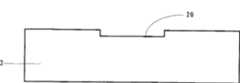
如图1所示,本发明的可减小短沟道效应的MOS晶体管1制作在硅衬底2上,所述硅衬底2上已制成了场隔离区(未图示),所述可减小短沟道效应的MOS晶体管1包括栅极堆层10、栅极侧墙11、源极12、漏极13、轻掺杂漏(LDD)结构14、晕注入(halo)结构15。As shown in Fig. 1, the MOS transistor 1 that can reduce the short channel effect of the present invention is made on the
所述栅极堆层10包括栅极绝缘层100和栅极102。所述硅衬底2上对应栅极堆层10制作有凹槽(未图示),所述凹槽的面积不小于所述栅极堆层10的面积,所述栅极堆层10设置在所述凹槽中。The
所述栅极侧墙11设置在栅极堆层10两侧,用于确保栅极堆层10与源极12和漏极13之间的绝缘。The
所述源极12和漏极13设置在硅衬底2内且排布在栅极10两侧,所述源极12和漏极13顶部具有金属硅化物层120和130。The
在本实施例中,通过浅沟槽隔离技术制成所述场隔离区,所述栅极绝缘层100为氧化硅层,所述栅极102为多晶硅栅极,所述栅极侧墙11由氧化硅制成。In this embodiment, the field isolation region is formed by shallow trench isolation technology, the
所述轻掺杂漏结构14和晕注入结构15均可在一定程度上减小短沟道效应,但不能彻底的解决短沟道效应。通过本发明的凹槽使得MOS晶体管1的沟道低于源极12和漏极13的平面,如此可有效减小短沟道效应。Both the lightly doped
参见图2,配合参见图1,本发明的可减小短沟道效应的MOS晶体管1的制作方法首先进行步骤S20,光刻出对应栅极堆层10的凹槽图形。参见图3,显示了完成步骤S20后硅衬底2的剖视图,如图所示,光阻3覆盖在硅衬底2,且光阻3上已生成有凹槽图形。Referring to FIG. 2 and referring to FIG. 1 , the manufacturing method of the MOS transistor 1 capable of reducing the short channel effect of the present invention firstly performs step S20 , where a groove pattern corresponding to the
接着继续步骤S21,通过刻蚀制成凹槽。在本实施例中,通过湿法刻蚀制成凹槽。参见图4,显示了完成步骤S21后硅衬底2的剖视图,如图所示,硅衬底2上制成了凹槽20。Then continue to step S21, forming grooves by etching. In this embodiment, the grooves are formed by wet etching. Referring to FIG. 4 , it shows a cross-sectional view of the
接着继续步骤S22,去除光刻胶并优化硅衬底2的表面。在本实施例中,通过氧化和湿法腐蚀工艺来优化硅衬底的表面。Then continue to step S22 , removing the photoresist and optimizing the surface of the
接着继续步骤S23,进行阱注入、防穿通注入和阈值电压调整注入。Next, step S23 is continued to perform well implantation, anti-puncture implantation and threshold voltage adjustment implantation.
接着继续步骤S24,在所述凹槽中制作栅极堆层10,所述栅极堆层10包括栅极绝缘层100和栅极102。在本实施例中,首先先沉积栅极绝缘层100,然后再沉积栅极102,最后经光刻和刻蚀制成栅极堆层10。Then continue to step S24 , forming a
接着继续步骤S25,进行轻掺杂漏注入和晕注入,以形成轻掺杂漏结构14和晕注入结构15。Then continue to step S25 , performing lightly doped drain implantation and halo implantation to form the lightly doped
接着继续步骤S26,制作栅极侧墙11。Then continue to step S26 to fabricate the
接着继续步骤S27,进行源漏注入,以制成源极12和漏极13。Then continue to step S27 , perform source-drain implantation to form the
接着继续步骤S28,在源极12和漏极13顶部制作金属硅化物层120和130。Then continue to step S28 , forming
需说明的是,步骤S20和步骤S24中,一般使用两张光罩形成所需的图形,也可使用相同的光罩但使用极性不同的光刻胶进行光刻,其中,在步骤S20中使用反光刻胶,在步骤S24中使用正光刻胶,如此可大大节约成本。It should be noted that, in step S20 and step S24, two photomasks are generally used to form the required pattern, and the same photomask but photoresists with different polarities can also be used for photolithography, wherein, in step S20 Using a reflective photoresist and using a positive photoresist in step S24 can greatly save costs.
综上所述,本发明的可减小短沟道效应的MOS晶体管1及其制作方法将栅极堆层制作在低于源漏极的凹槽中,以达成相对抬高源漏极的目的,从而可有效的减小短沟道效应,另外可降低工艺难度和制作成本,再者,可降低栅极堆层的高度,为后续金属前栅堆层间介质淀积工艺提供更大的工艺窗口。To sum up, the MOS transistor 1 capable of reducing the short channel effect of the present invention and its manufacturing method make the gate stack layer in the groove lower than the source and drain, so as to achieve the purpose of relatively raising the source and drain , so that the short channel effect can be effectively reduced, and the process difficulty and production cost can be reduced. Moreover, the height of the gate stack can be reduced, providing a larger process for the subsequent metal front gate stack interlayer dielectric deposition process. window.
Claims (9)
Priority Applications (3)
| Application Number | Priority Date | Filing Date | Title |
|---|---|---|---|
| CN2007100391861ACN101030602B (en) | 2007-04-06 | 2007-04-06 | MOS transistor for decreasing short channel and its production |
| US12/062,851US20080246087A1 (en) | 2007-04-06 | 2008-04-04 | Mos transistor for reducing short-channel effects and its production |
| US12/946,162US8193057B2 (en) | 2007-04-06 | 2010-11-15 | MOS transistor for reducing short-channel effects and its production |
Applications Claiming Priority (1)
| Application Number | Priority Date | Filing Date | Title |
|---|---|---|---|
| CN2007100391861ACN101030602B (en) | 2007-04-06 | 2007-04-06 | MOS transistor for decreasing short channel and its production |
Publications (2)
| Publication Number | Publication Date |
|---|---|
| CN101030602A CN101030602A (en) | 2007-09-05 |
| CN101030602Btrue CN101030602B (en) | 2012-03-21 |
Family
ID=38715791
Family Applications (1)
| Application Number | Title | Priority Date | Filing Date |
|---|---|---|---|
| CN2007100391861AActiveCN101030602B (en) | 2007-04-06 | 2007-04-06 | MOS transistor for decreasing short channel and its production |
Country Status (2)
| Country | Link |
|---|---|
| US (2) | US20080246087A1 (en) |
| CN (1) | CN101030602B (en) |
Families Citing this family (57)
| Publication number | Priority date | Publication date | Assignee | Title |
|---|---|---|---|---|
| WO2007003220A1 (en)* | 2005-06-30 | 2007-01-11 | Freescale Semiconductor, Inc | Method of forming a semiconductor structure |
| CN101783324B (en)* | 2009-01-19 | 2012-03-07 | 中芯国际集成电路制造(上海)有限公司 | CMOS (complementary metal-oxide-semiconductor) transistor and manufacturing method thereof |
| US8421162B2 (en) | 2009-09-30 | 2013-04-16 | Suvolta, Inc. | Advanced transistors with punch through suppression |
| US20110079861A1 (en)* | 2009-09-30 | 2011-04-07 | Lucian Shifren | Advanced Transistors with Threshold Voltage Set Dopant Structures |
| US8273617B2 (en) | 2009-09-30 | 2012-09-25 | Suvolta, Inc. | Electronic devices and systems, and methods for making and using the same |
| US8530286B2 (en) | 2010-04-12 | 2013-09-10 | Suvolta, Inc. | Low power semiconductor transistor structure and method of fabrication thereof |
| US8569128B2 (en) | 2010-06-21 | 2013-10-29 | Suvolta, Inc. | Semiconductor structure and method of fabrication thereof with mixed metal types |
| US8759872B2 (en) | 2010-06-22 | 2014-06-24 | Suvolta, Inc. | Transistor with threshold voltage set notch and method of fabrication thereof |
| US8377783B2 (en) | 2010-09-30 | 2013-02-19 | Suvolta, Inc. | Method for reducing punch-through in a transistor device |
| CN102487085B (en)* | 2010-12-01 | 2014-04-23 | 中国科学院微电子研究所 | Semiconductor device and method for manufacturing the same |
| US8404551B2 (en) | 2010-12-03 | 2013-03-26 | Suvolta, Inc. | Source/drain extension control for advanced transistors |
| US8461875B1 (en) | 2011-02-18 | 2013-06-11 | Suvolta, Inc. | Digital circuits having improved transistors, and methods therefor |
| US8525271B2 (en) | 2011-03-03 | 2013-09-03 | Suvolta, Inc. | Semiconductor structure with improved channel stack and method for fabrication thereof |
| US8400219B2 (en) | 2011-03-24 | 2013-03-19 | Suvolta, Inc. | Analog circuits having improved transistors, and methods therefor |
| US8748270B1 (en) | 2011-03-30 | 2014-06-10 | Suvolta, Inc. | Process for manufacturing an improved analog transistor |
| US8999861B1 (en) | 2011-05-11 | 2015-04-07 | Suvolta, Inc. | Semiconductor structure with substitutional boron and method for fabrication thereof |
| US8796048B1 (en) | 2011-05-11 | 2014-08-05 | Suvolta, Inc. | Monitoring and measurement of thin film layers |
| US8811068B1 (en) | 2011-05-13 | 2014-08-19 | Suvolta, Inc. | Integrated circuit devices and methods |
| US8569156B1 (en) | 2011-05-16 | 2013-10-29 | Suvolta, Inc. | Reducing or eliminating pre-amorphization in transistor manufacture |
| US8735987B1 (en) | 2011-06-06 | 2014-05-27 | Suvolta, Inc. | CMOS gate stack structures and processes |
| US8995204B2 (en) | 2011-06-23 | 2015-03-31 | Suvolta, Inc. | Circuit devices and methods having adjustable transistor body bias |
| US8629016B1 (en) | 2011-07-26 | 2014-01-14 | Suvolta, Inc. | Multiple transistor types formed in a common epitaxial layer by differential out-diffusion from a doped underlayer |
| US8748986B1 (en) | 2011-08-05 | 2014-06-10 | Suvolta, Inc. | Electronic device with controlled threshold voltage |
| KR101891373B1 (en) | 2011-08-05 | 2018-08-24 | 엠아이이 후지쯔 세미컨덕터 리미티드 | Semiconductor devices having fin structures and fabrication methods thereof |
| CN102931235B (en)* | 2011-08-12 | 2016-02-17 | 中芯国际集成电路制造(上海)有限公司 | MOS transistor and manufacture method thereof |
| US8614128B1 (en) | 2011-08-23 | 2013-12-24 | Suvolta, Inc. | CMOS structures and processes based on selective thinning |
| US8645878B1 (en) | 2011-08-23 | 2014-02-04 | Suvolta, Inc. | Porting a circuit design from a first semiconductor process to a second semiconductor process |
| US8713511B1 (en) | 2011-09-16 | 2014-04-29 | Suvolta, Inc. | Tools and methods for yield-aware semiconductor manufacturing process target generation |
| US9236466B1 (en) | 2011-10-07 | 2016-01-12 | Mie Fujitsu Semiconductor Limited | Analog circuits having improved insulated gate transistors, and methods therefor |
| CN103151292B (en)* | 2011-12-07 | 2015-04-08 | 上海华虹宏力半导体制造有限公司 | Integrated method of raise source leakage structure complementary metal-oxide-semiconductor transistor (CMOS) and Bipolar device |
| US8895327B1 (en) | 2011-12-09 | 2014-11-25 | Suvolta, Inc. | Tipless transistors, short-tip transistors, and methods and circuits therefor |
| US8819603B1 (en) | 2011-12-15 | 2014-08-26 | Suvolta, Inc. | Memory circuits and methods of making and designing the same |
| US8883600B1 (en) | 2011-12-22 | 2014-11-11 | Suvolta, Inc. | Transistor having reduced junction leakage and methods of forming thereof |
| US8599623B1 (en) | 2011-12-23 | 2013-12-03 | Suvolta, Inc. | Circuits and methods for measuring circuit elements in an integrated circuit device |
| US8877619B1 (en) | 2012-01-23 | 2014-11-04 | Suvolta, Inc. | Process for manufacture of integrated circuits with different channel doping transistor architectures and devices therefrom |
| US8970289B1 (en) | 2012-01-23 | 2015-03-03 | Suvolta, Inc. | Circuits and devices for generating bi-directional body bias voltages, and methods therefor |
| US9093550B1 (en) | 2012-01-31 | 2015-07-28 | Mie Fujitsu Semiconductor Limited | Integrated circuits having a plurality of high-K metal gate FETs with various combinations of channel foundation structure and gate stack structure and methods of making same |
| US9406567B1 (en) | 2012-02-28 | 2016-08-02 | Mie Fujitsu Semiconductor Limited | Method for fabricating multiple transistor devices on a substrate with varying threshold voltages |
| US8863064B1 (en) | 2012-03-23 | 2014-10-14 | Suvolta, Inc. | SRAM cell layout structure and devices therefrom |
| US9299698B2 (en) | 2012-06-27 | 2016-03-29 | Mie Fujitsu Semiconductor Limited | Semiconductor structure with multiple transistors having various threshold voltages |
| US8637955B1 (en) | 2012-08-31 | 2014-01-28 | Suvolta, Inc. | Semiconductor structure with reduced junction leakage and method of fabrication thereof |
| US9112057B1 (en) | 2012-09-18 | 2015-08-18 | Mie Fujitsu Semiconductor Limited | Semiconductor devices with dopant migration suppression and method of fabrication thereof |
| US9041126B2 (en) | 2012-09-21 | 2015-05-26 | Mie Fujitsu Semiconductor Limited | Deeply depleted MOS transistors having a screening layer and methods thereof |
| CN102931067B (en)* | 2012-10-30 | 2015-01-28 | 中国电子科技集团公司第五十五研究所 | Method for reducing damages of silicon carbide groove to improve reliability of schottky grating |
| US9431068B2 (en) | 2012-10-31 | 2016-08-30 | Mie Fujitsu Semiconductor Limited | Dynamic random access memory (DRAM) with low variation transistor peripheral circuits |
| US8816754B1 (en) | 2012-11-02 | 2014-08-26 | Suvolta, Inc. | Body bias circuits and methods |
| US9093997B1 (en) | 2012-11-15 | 2015-07-28 | Mie Fujitsu Semiconductor Limited | Slew based process and bias monitors and related methods |
| US9070477B1 (en) | 2012-12-12 | 2015-06-30 | Mie Fujitsu Semiconductor Limited | Bit interleaved low voltage static random access memory (SRAM) and related methods |
| US9112484B1 (en) | 2012-12-20 | 2015-08-18 | Mie Fujitsu Semiconductor Limited | Integrated circuit process and bias monitors and related methods |
| US9268885B1 (en) | 2013-02-28 | 2016-02-23 | Mie Fujitsu Semiconductor Limited | Integrated circuit device methods and models with predicted device metric variations |
| US9299801B1 (en) | 2013-03-14 | 2016-03-29 | Mie Fujitsu Semiconductor Limited | Method for fabricating a transistor device with a tuned dopant profile |
| US9478571B1 (en) | 2013-05-24 | 2016-10-25 | Mie Fujitsu Semiconductor Limited | Buried channel deeply depleted channel transistor |
| KR20150000546A (en)* | 2013-06-24 | 2015-01-05 | 삼성전자주식회사 | Semiconductor device and method for fabricating the same |
| US20150187915A1 (en)* | 2013-12-26 | 2015-07-02 | Samsung Electronics Co., Ltd. | Method for fabricating fin type transistor |
| US9710006B2 (en) | 2014-07-25 | 2017-07-18 | Mie Fujitsu Semiconductor Limited | Power up body bias circuits and methods |
| US9319013B2 (en) | 2014-08-19 | 2016-04-19 | Mie Fujitsu Semiconductor Limited | Operational amplifier input offset correction with transistor threshold voltage adjustment |
| CN105185799A (en)* | 2015-08-18 | 2015-12-23 | 格科微电子(上海)有限公司 | Back-illuminated image sensor with three-dimensional transistor structure and forming method thereof |
Citations (2)
| Publication number | Priority date | Publication date | Assignee | Title |
|---|---|---|---|---|
| CN1428845A (en)* | 2001-12-26 | 2003-07-09 | 东部电子株式会社 | Transistor forming method |
| US7081652B2 (en)* | 2004-04-14 | 2006-07-25 | Kabushiki Kaisha Toshiba | Semiconductor device having a side wall insulating film and a manufacturing method thereof |
Family Cites Families (10)
| Publication number | Priority date | Publication date | Assignee | Title |
|---|---|---|---|---|
| US4065783A (en)* | 1976-10-18 | 1977-12-27 | Paul Hsiung Ouyang | Self-aligned double implanted short channel V-groove MOS device |
| FR2625044B1 (en)* | 1987-12-18 | 1990-08-31 | Commissariat Energie Atomique | TRANSISTOR MOS WITH END OF DIELECTRIC INTERFACE OF GRID / RAISED SUBSTRATE AND MANUFACTURING METHOD THEREOF |
| DE4400842C2 (en)* | 1994-01-13 | 1998-03-26 | Gold Star Electronics | MOS transistor and method for its manufacture |
| US5448094A (en)* | 1994-08-23 | 1995-09-05 | United Microelectronics Corp. | Concave channel MOS transistor and method of fabricating the same |
| JP3461277B2 (en)* | 1998-01-23 | 2003-10-27 | 株式会社東芝 | Semiconductor device and manufacturing method thereof |
| US6130454A (en)* | 1998-07-07 | 2000-10-10 | Advanced Micro Devices, Inc. | Gate conductor formed within a trench bounded by slanted sidewalls |
| US6887762B1 (en)* | 1998-11-12 | 2005-05-03 | Intel Corporation | Method of fabricating a field effect transistor structure with abrupt source/drain junctions |
| US6956263B1 (en)* | 1999-12-28 | 2005-10-18 | Intel Corporation | Field effect transistor structure with self-aligned raised source/drain extensions |
| JP3651802B2 (en)* | 2002-09-12 | 2005-05-25 | 株式会社東芝 | Manufacturing method of semiconductor device |
| KR100526478B1 (en)* | 2003-12-31 | 2005-11-08 | 동부아남반도체 주식회사 | Semiconductor device and fabricating method thereof |
- 2007
- 2007-04-06CNCN2007100391861Apatent/CN101030602B/enactiveActive
- 2008
- 2008-04-04USUS12/062,851patent/US20080246087A1/ennot_activeAbandoned
- 2010
- 2010-11-15USUS12/946,162patent/US8193057B2/enactiveActive
Patent Citations (2)
| Publication number | Priority date | Publication date | Assignee | Title |
|---|---|---|---|---|
| CN1428845A (en)* | 2001-12-26 | 2003-07-09 | 东部电子株式会社 | Transistor forming method |
| US7081652B2 (en)* | 2004-04-14 | 2006-07-25 | Kabushiki Kaisha Toshiba | Semiconductor device having a side wall insulating film and a manufacturing method thereof |
Also Published As
| Publication number | Publication date |
|---|---|
| US8193057B2 (en) | 2012-06-05 |
| US20080246087A1 (en) | 2008-10-09 |
| CN101030602A (en) | 2007-09-05 |
| US20110059588A1 (en) | 2011-03-10 |
Similar Documents
| Publication | Publication Date | Title |
|---|---|---|
| CN101030602B (en) | MOS transistor for decreasing short channel and its production | |
| KR101057651B1 (en) | Method of manufacturing semiconductor device | |
| JP2009514220A5 (en) | ||
| CN107919324A (en) | The forming method of semiconductor devices | |
| CN107403721A (en) | Method for manufacturing power metal oxide semiconductor field effect transistor | |
| WO2017008331A1 (en) | Tft substrate structure and manufacturing method therefor | |
| CN110416085A (en) | Semi-floating gate transistor with SiGe channel structure and manufacturing method thereof | |
| US7001817B2 (en) | Method for fabricating a semiconductor device | |
| US20080160698A1 (en) | Method for fabricating a semiconductor device | |
| US7674677B2 (en) | Semiconductor device and a method for manufacturing the same | |
| TWI750375B (en) | Trench gate mosfet and method of forming the same | |
| KR101060697B1 (en) | MOS transistor with increased channel width and manufacturing method thereof | |
| CN114121667B (en) | Method for manufacturing semiconductor device | |
| CN104218080A (en) | Radio frequency LDMOS device and manufacturing method thereof | |
| CN104217933B (en) | Semiconductor structure and forming method thereof | |
| CN112951913B (en) | Semiconductor structure and method of forming the same | |
| US8637939B2 (en) | Semiconductor device and method for fabricating the same | |
| US7186603B2 (en) | Method of forming notched gate structure | |
| CN100390947C (en) | Metal oxide semiconductor field effect transistor and its manufacturing method | |
| KR20060001327A (en) | Method for manufacturing a semiconductor device containing fiFFT | |
| US20060145259A1 (en) | Fin field-effect transistor and method for fabricating the same | |
| CN104008976A (en) | Manufacturing method of groove power device | |
| KR101643338B1 (en) | Method for fabricating of the trench gate mosfet | |
| KR100365416B1 (en) | Manufacturing method of semiconductor device | |
| KR100800922B1 (en) | Transistor manufacturing method of semiconductor device |
Legal Events
| Date | Code | Title | Description |
|---|---|---|---|
| C06 | Publication | ||
| PB01 | Publication | ||
| C10 | Entry into substantive examination | ||
| SE01 | Entry into force of request for substantive examination | ||
| C14 | Grant of patent or utility model | ||
| GR01 | Patent grant |